6.776 high speed communication circuits lecture 11 noise ... · -a transformer does not alleviate...
TRANSCRIPT

6.776High Speed Communication Circuits
Lecture 11Noise Figure, Impact of Amplifier Nonlinearities
Michael PerrottMassachusetts Institute of Technology
March 10, 2005
Copyright © 2005 by Michael H. Perrott

H.-S. Lee & M.H. Perrott MIT OCW
Noise Factor and Noise Figure (From Lec 10)
Definitions
Calculation of SNRin and SNRout
iout
RsenRs
vin
Linear,Time Invariant Circuit
(Noiseless)Zin
vxZL
inoutZout
Equivalent outputreferred current noise
(assumed to be independentof Zout and ZL)

H.-S. Lee & M.H. Perrott MIT OCW
Alternative Noise Factor Expression
From previous slide
Calculation of Noise Factor
iout
RsenRs
vin
Linear,Time Invariant Circuit
(Noiseless)Zin
vxZL
inoutZout
Equivalent outputreferred current noise
(assumed to be independentof Zout and ZL)

H.-S. Lee & M.H. Perrott MIT OCW
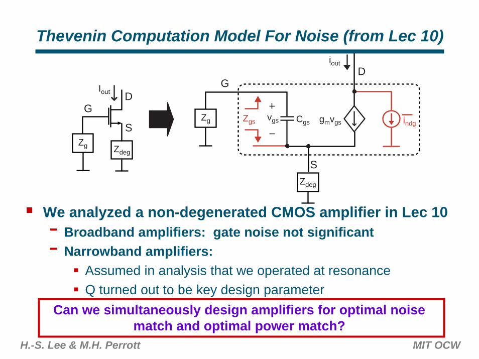
Thevenin Computation Model For Noise (from Lec 10)
Iout
GD
Svgs gmvgsCgs indg
D
S
G
ZgsZg
Zdeg
iout
Zg Zdeg
H.-S. Lee & M.H. Perrott MIT OCW
Thevenin Computation Model For Noise (from Lec 10)
Iout
GD
Svgs gmvgsCgs indg
D
S
G
ZgsZg
Zdeg
iout
Zg Zdeg
We analyzed a non-degenerated CMOS amplifier in Lec 10- Broadband amplifiers: gate noise not significant- Narrowband amplifiers:
Assumed in analysis that we operated at resonanceQ turned out to be key design parameter
Can we simultaneously design amplifiers for optimal noise match and optimal power match?

H.-S. Lee & M.H. Perrott MIT OCW
Input Referred Noise Model
iout
RsenRs
vin
Linear,Time Invariant Circuit
(Noiseless)Zin
vxZL
inoutZout
Equivalent outputreferred current noise
(assumed to be independentof Zout and ZL)
iout
Linear,Time Invariant Circuit
(Noiseless)Zin
vxinYsisiin
en
inYsis
Can remove the signal sourcesince Noise Factor can be
expressed as the ratio of total output noise to input noise
iin,sc=ioutβ
en

H.-S. Lee & M.H. Perrott MIT OCW
Input-Referred Noise Figure Expression
We know that
Let’s express the above in terms of input short circuit current
en
inYsis iin,sc=ioutβ

H.-S. Lee & M.H. Perrott MIT OCW
Calculation of Noise Factor
en
inYsis iin,sc=ioutβ
By inspection of above figure
In general, en and in will be correlated
- Yc is called the correlation admittance

H.-S. Lee & M.H. Perrott MIT OCW
Noise Factor Expressed in Terms of Admittances
iuYc
en
Ysis iin,sc=ioutβ
We can replace voltage and current noise currents with impedances and admittances

H.-S. Lee & M.H. Perrott MIT OCW
Optimal Source Admittance for Minimum Noise Factor
Take the derivative with respect to source admittance and set to zero (to find minimum F), which yields
Plug these values into expression above to obtain
Express admittances as the sum of conductance, G, and susceptance, B

H.-S. Lee & M.H. Perrott MIT OCW
Optimal Source Admittance for Minimum Noise Factor
After much algebra (see Appendix L of Gonzalez* book for derivation), we can derive
- Contours of constant noise factor are circles centered about (Gopt,Bopt) in the admittance plane- They are also circles on a Smith Chart (see pp 299-302 of Gonzalez for derivation and examples)
How does (Gopt,Bopt) compare to admittance achieving maximum power transfer?
*Guillermo Gonzalez, Microwave Transistor Amplifiers: Analysis and Design, Prentice Hall, 1996

H.-S. Lee & M.H. Perrott MIT OCW
Optimizing For Noise Figure versus Power Transfer
Gs
Bs
Gopt
Bopt
Example sourceadmittance for maximum
power transfer Circles of constantNoise Factor
(Fmin at the center)
iout
Linear,Time Invariant Circuit
(Noiseless)Zin
vxinGsisiin
en
Bs
Signal
Source noise producedby source conductance
Sourcesusceptance
Sourceconductance
Bmax
Gmax
One cannot generally achieve minimum noise figure if maximum power transfer is desired

H.-S. Lee & M.H. Perrott MIT OCW
Optimal Noise Factor for MOS Transistor Amp
Consider the common source MOS amp (no degeneration) considered in Lecture 10- In Tom Lee’s book (pp. 272-276 (1st ed.), pp. 364-369 (2nd
ed.)), the noise impedances are derived as
- The optimal source admittance values to minimize noise factor are therefore

H.-S. Lee & M.H. Perrott MIT OCW
Optimal Noise Factor for MOS Transistor Amp (Cont.)
Optimal admittance consists of a resistor and inductor (wrong frequency behavior – broadband match fundamentally difficult)
- If there is zero correlation, inductor value should be set to resonate with Cgs at frequency of operation
Minimum noise figure
- Exact if one defines wt = gm/Cgs

H.-S. Lee & M.H. Perrott MIT OCW
Recall Noise Factor Comparison Plot From Lecture 10
1 2 3 4 5 6 7 8 9 100
1
2
3
4
5
6
7
8
Q
Noi
se F
acto
r Sca
ling
Coe
ffici
ent
Noise Factor Scaling Coefficient Versus Q for 0.18µ NMOS Device
c = -j0
c = -j0.55
c = -j1
c = -j1
c = -j0.55c = -j0
Minimum acrossall values of Q and
Achievable values asa function of Q under
the constraint that
LgCgs
1= wo
LgCgs
1
Note: curvesmeet if we
approximateQ2+1 Q2

H.-S. Lee & M.H. Perrott MIT OCW
Example: Noise Factor Calculation for Resistor Load
Total output noise
Total output noise due to source
Noise Factor
vin
Rs
RL
Source
vout
enRs
enRL
Rs
RL
Source
vnout

H.-S. Lee & M.H. Perrott MIT OCW
Comparison of Noise Figure and Power Match
vin
Rs
RL
Source
vout
enRs
enRL
Rs
RL
Source
vnout
To achieve minimum Noise Factor
To achieve maximum power transfer

H.-S. Lee & M.H. Perrott MIT OCW
Example: Noise Factor Calculation for Capacitor Load
vin
Rs
CL
Source
vout
enRsRs
Source
vnoutCL
Total output noise
Total output noise due to source
Noise Factor

H.-S. Lee & M.H. Perrott MIT OCW
Example: Noise Factor with Zero Source Resistance
vin
RL
CL
Source
vout
enRLRL
vnoutCL
Total output noise
Total output noise due to source
Noise Factor
H.-S. Lee & M.H. Perrott MIT OCW
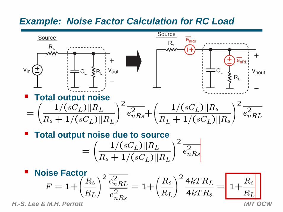
Example: Noise Factor Calculation for RC Load
Total output noise
Total output noise due to source
Noise Factor
vin
Rs
CL
Source
vout
enRsRs
Source
vnoutCLRL
enRL
RL

H.-S. Lee & M.H. Perrott MIT OCW
Example: Resistive Load with Source Transformer
Vs
RS
RLVx
1:N
Source
Rin= N21 RL Rout=N2Rs
Vout=NVx
enRs
enRL
RL
RS
Vx
1:N
Source
Rin= N21 RL Rout=N2Rs
Vnout=NVx
For maximum power transfer (as derived in Lecture 3)

H.-S. Lee & M.H. Perrott MIT OCW
Noise Factor with Transformer Set for Max Power Transfer
Total output noise
Total output noise due to source
enRs
enRL
RL
RS
Vx
1:N=
Source
Rin= Rs Rout=RLVnout= Vx
RLRs
RLRs
Noise Factor

H.-S. Lee & M.H. Perrott MIT OCW
Observations
enRs
enRL
RL
RS
Vx
1:N=
Source
Rin= Rs Rout=RLVnout= Vx
RLRs
RLRs
If you need to power match to a resistive load, you must pay a 3 dB penalty in Noise Figure- A transformer does not alleviate this issue
What value does a transformer provide?- Almost-true answer: maximizes voltage gain given the
power match constraint, thereby reducing effect of noise of following amplifiers
- Accurate answer: we need to wait until we talk about cascaded noise factor calculations

H.-S. Lee & M.H. Perrott MIT OCW
Nonlinearities in Amplifiers
We can generally break up an amplifier into the cascade of a memoryless nonlinearity and an input and/or output transfer function
Impact of nonlinearities with sine wave input- Causes harmonic distortion (i.e., creation of harmonics)
Impact of nonlinearities with several sine wave inputs- Causes harmonic distortion for each input AND
intermodulation products
M1
RLVout
CL
IdVin
Vdd MemorylessNonlinearity
1+sRLCL
Vin
LowpassFilter
VoutId -RL

H.-S. Lee & M.H. Perrott MIT OCW
Analysis of Amplifier Nonlinearities
Focus on memoryless nonlinearity block- The impact of filtering can be added later
Model nonlinearity as a Taylor series expansion up to its third order term (assumes small signal variation)
- For harmonic distortion, consider
- For intermodulation, consider
MemorylessNonlinearity
x y

H.-S. Lee & M.H. Perrott MIT OCW
Harmonic Distortion
Substitute x(t) into polynomial expression
Fundamental Harmonics
Notice that each harmonic term, cos(nwt), has an amplitude that grows in proportion to An
- Very small for small A, very large for large A

H.-S. Lee & M.H. Perrott MIT OCW
Frequency Domain View of Harmonic Distortion
MemorylessNonlinearity
x yw
A
0 w
c1A +
0 2w 3w
3c3A3
4Afund =
Harmonics cause “noise”- Their impact depends highly on application
LNA – typically not of consequencePower amp – can degrade spectral maskAudio amp – depends on your listening preference!
Gain for fundamental component depends on input amplitude!

H.-S. Lee & M.H. Perrott MIT OCW
1 dB Compression Point
MemorylessNonlinearity
x yw
A
0 w
c1A +
0 2w 3w
3c3A3
4Afund =
Definition: input signal level such that the small-signal gain drops by 1 dB- Input signal level is high! A1-dB
1 dB
20log(A)
20log(Afund)
Typically calculated from simulation or measurement rather than analytically- Analytical model must include many more terms in Taylor
series to be accurate in this context

H.-S. Lee & M.H. Perrott MIT OCW
Harmonic Products with An Input of Two Sine Waves
DC and fundamental components
Second and third harmonic terms
Similar result as having an input with one sine wave- But, we haven’t yet considered cross terms!

H.-S. Lee & M.H. Perrott MIT OCW
Intermodulation Products
Second-order intermodulation (IM2) products
Third-order intermodulation (IM3) products
- These are the troublesome ones for narrowband systems
H.-S. Lee & M.H. Perrott MIT OCW
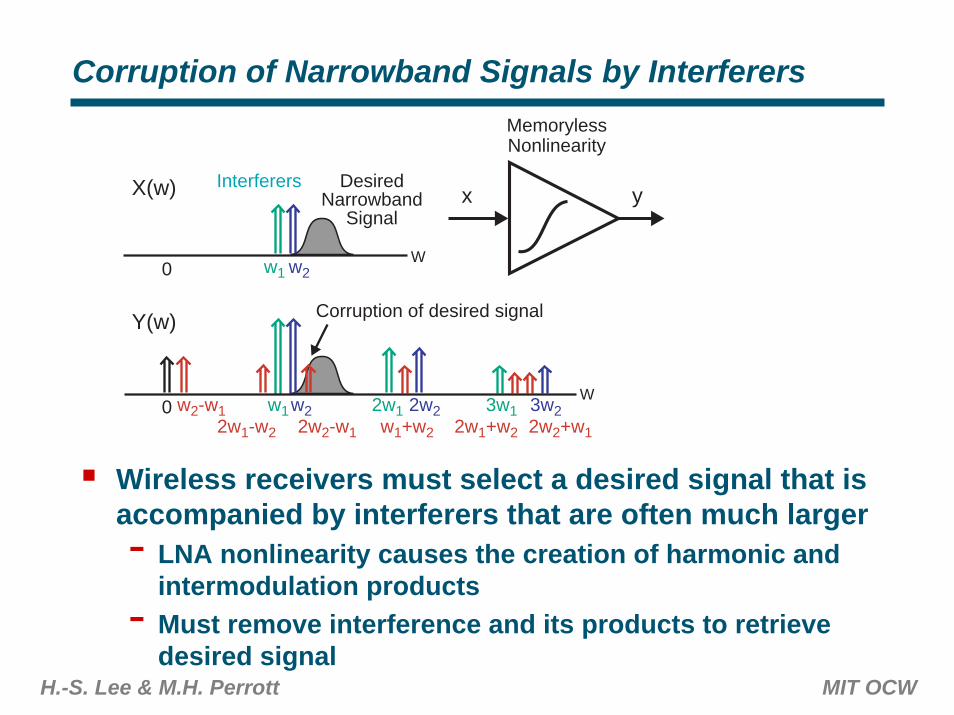
Corruption of Narrowband Signals by InterferersMemorylessNonlinearity
x y
w10 w2W
X(w) DesiredNarrowband
Signal
Interferers
0 w12w2+w1
w2 2w22w1-w2 2w1+w22w2-w1 w1+w2
w2-w1 2w1 3w23w1W
Y(w) Corruption of desired signal
Wireless receivers must select a desired signal that is accompanied by interferers that are often much larger- LNA nonlinearity causes the creation of harmonic and
intermodulation products- Must remove interference and its products to retrieve
desired signal

H.-S. Lee & M.H. Perrott MIT OCW
Use Filtering to Remove Undesired InterferenceMemorylessNonlinearity
x y
w10 w2W
X(w) DesiredNarrowband
Signal
Interferers
0 w12w2+w1
w2 2w22w1-w2 2w1+w22w2-w1 w1+w2
w2-w1 2w1 3w23w1W
Y(w) Corruption of desired signal
0 w12w2+w1
w2 2w22w1-w2 2w1+w22w2-w1 w1+w2
w2-w1 2w1 3w23w1W
Z(w) Corruption of desired signal
BandpassFilter
z
Ineffective for IM3 term that falls in the desired signal frequency band

H.-S. Lee & M.H. Perrott MIT OCW
Characterization of Intermodulation
Magnitude of third order products is set by c3 and input signal amplitude (for small A)
Magnitude of first order term is set by c1 and A (for small A)
Relative impact of intermodulation products can be calculated once we know A and the ratio of c3 to c1- Problem: it’s often hard to extract the polynomial
coefficients through direct DC measurementsNeed an indirect way to measure the ratio of c3 to c1

H.-S. Lee & M.H. Perrott MIT OCW
Two Tone Test
Input the sum of two equal amplitude sine waves into the amplifier (assume Zin of amplifier = Rs of source)
On a spectrum analyzer, measure first order and third order terms as A is varied (A must remain small)- First order term will increase linearly- Third order IM term will increase as the cube of A
w10 w2W
vin(w)Equal Amplitude
Sine Waves
0 w12w2+w1
w2 2w22w1-w2 2w1+w22w2-w1 w1+w2
w2-w1 2w1 3w23w1W
Vout(w)first-order outputthird-order IM term
Amplifier
vin
Rs
Zin=Rs
Vout
Vbias
2A Vx
Vout=co+c1Vx+c2Vx+c3Vx2 3
Note:vx(w) =
vin(w)2
H.-S. Lee & M.H. Perrott MIT OCW
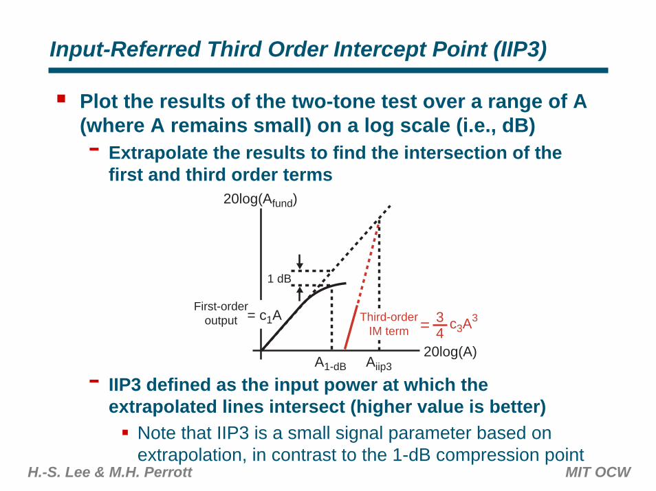
Input-Referred Third Order Intercept Point (IIP3)
Plot the results of the two-tone test over a range of A (where A remains small) on a log scale (i.e., dB)- Extrapolate the results to find the intersection of the
first and third order terms
- IIP3 defined as the input power at which the extrapolated lines intersect (higher value is better)
Note that IIP3 is a small signal parameter based on extrapolation, in contrast to the 1-dB compression point
A1-dB
1 dB
20log(A)
20log(Afund)
Aiip3
Third-orderIM term
First-orderoutput c3A33
4== c1A

H.-S. Lee & M.H. Perrott MIT OCW
Relationship between IIP3, c1 and c3
Intersection point
Solve for A (gives Aiip3)
Note that A corresponds to the peak value of the two cosine waves coming into the amplifier input node (Vx)- Would like to instead like to express IIP3 in terms of power
A1-dB
1 dB
20log(A)
20log(Afund)
Aiip3
Third-orderIM term
First-orderoutput c3A33
4== c1A

H.-S. Lee & M.H. Perrott MIT OCW
IIP3 Expressed in Terms of Power at Source
IIP3 referenced to Vx (peak voltage)
IIP3 referenced to Vx(rms voltage)
w10 w2W
vin(w)Equal Amplitude
Sine WavesAmplifier
vin
Rs
Zin=Rs
Vout
Vbias
2AVx
Vout=co+c1Vx+c2Vx+c3Vx2 3
Note:vx(w) =
vin(w)2
Power across Zin = Rs Note: Power from vin

H.-S. Lee & M.H. Perrott MIT OCW
IIP3 as a Benchmark Specification
Since IIP3 is a convenient parameter to describe the level of third order nonlinearity in an amplifier, it is often quoted as a benchmark specMeasurement of IIP3 on a discrete amplifier would be done using the two-tone method described earlier- This is rarely done on integrated amplifiers due to poor
access to the key nodes- Instead, for a radio receiver for instance, one would simply
put in interferers and see how the receiver doesNote: performance in the presence of interferers is not just a function of the amplifier nonlinearity
Calculation of IIP3 is most easily done using a simulator such as Hspice or Spectre- Two-tone method is theoretically not necessary – simply
curve fit to a third order polynomial

H.-S. Lee & M.H. Perrott MIT OCW
Impact of Differential Amplifiers on Nonlinearity
M1 M2
2Ibias
vid
I1 I2
2-vid
2vx
MemorylessNonlinearity
vid Idiff = I2-I1
Assume vx is approximately incremental ground
Second order term removed and IIP3 increased!