64/44-pin 8-bit mcu with 32 to 60k flash/rom, adc, five ... · march 2009 rev 2 1/193 st72321rx...
TRANSCRIPT
ST72321RxST72321ARx ST72321Jx
64/44-pin 8-bit MCU with 32 to 60K Flash/ROM, ADC,five timers, SPI, SCI, I2C interface
Features■ Memories
– 32K to 60K dual voltage High Density Flash(HDFlash) or ROM with read-out protectioncapability. In-Application Programming andIn-Circuit Programming for HDFlash devices
– 1K to 2K RAM– HDFlash endurance: 100 cycles, data reten-
tion: 40 years at 85°C■ Clock, Reset And Supply Management
– Enhanced low voltage supervisor (LVD) formain supply and auxiliar voltage detector(AVD) with interrupt capability
– Clock sources: crystal/ceramic resonator os-cillators, internal RC oscillator and bypass forexternal clock
– PLL for 2x frequency multiplication– Four Power Saving Modes: Halt, Active-Halt,
Wait and Slow■ Interrupt Management
– Nested interrupt controller– 14 interrupt vectors plus TRAP and RESET– Top Level Interrupt (TLI) pin on 64-pin devices– 15/9 external interrupt lines (on 4 vectors)
■ Up to 48 I/O Ports– 48/32/24 multifunctional bidirectional I/O lines– 34/22/17 alternate function lines– 16/12/10 high sink outputs
■ 5 Timers– Main Clock Controller with: Real time base,
Beep and Clock-out capabilities– Configurable watchdog timer– Two 16-bit timers with: 2 input captures, 2 out-
put compares, external clock input on one tim-er, PWM and pulse generator modes
– 8-bit PWM Auto-reload timer with: 2 input cap-tures, 4 PWM outputs, output compare andtime base interrupt, external clock with eventdetector
■ 3 Communications Interfaces– SPI synchronous serial interface– SCI asynchronous serial interface – I2C multimaster interface
■ 1 Analog peripheral– 10-bit ADC with up to 16 input ports
■ Instruction Set– 8-bit Data Manipulation– 63 Basic Instructions– 17 main Addressing Modes– 8 x 8 Unsigned Multiply Instruction
■ Development Tools– Full hardware/software development package– In-Circuit Testing capability
Table 1. Device summary
LQFP6410 x 10
LQFP6414 x 14
LQFP4410 x 10
LQFP327 x 7
Features ST72321R9/ST72321AR9/ ST72321J9
ST72321R7/ST72321AR7/ ST72321J7 ST72321R6/ST72321AR6
Program memory - bytes Flash/ROM 60K Flash/ROM 48K Flash/ROM 32KRAM (stack) - bytes 2048 (256) 1536 (256) 1024 (256)Operating Voltage 3.8 to 5.5V Temp. Range -40 to +125°C, -40 to +85°C Package LQFP64 14x14 (R), LQFP64 10x10 (AR), LQFP44 10x10 (J)
March 2009 Rev 2 1/193
1

Table of Contents
193
1 DESCRIPTION . . . . . . . . . . . . . . . . . . . . . . . . . . . . . . . . . . . . . . . . . . . . . . . . . . . . . . . . . . . . . . . 72 PIN DESCRIPTION . . . . . . . . . . . . . . . . . . . . . . . . . . . . . . . . . . . . . . . . . . . . . . . . . . . . . . . . . . . . 83 REGISTER & MEMORY MAP . . . . . . . . . . . . . . . . . . . . . . . . . . . . . . . . . . . . . . . . . . . . . . . . . . . 144 FLASH PROGRAM MEMORY . . . . . . . . . . . . . . . . . . . . . . . . . . . . . . . . . . . . . . . . . . . . . . . . . . 18
4.1 INTRODUCTION . . . . . . . . . . . . . . . . . . . . . . . . . . . . . . . . . . . . . . . . . . . . . . . . . . . . . . . . 18
4.2 MAIN FEATURES . . . . . . . . . . . . . . . . . . . . . . . . . . . . . . . . . . . . . . . . . . . . . . . . . . . . . . . 18
4.3 STRUCTURE . . . . . . . . . . . . . . . . . . . . . . . . . . . . . . . . . . . . . . . . . . . . . . . . . . . . . . . . . . . 18
4.3.1 Read-out Protection . . . . . . . . . . . . . . . . . . . . . . . . . . . . . . . . . . . . . . . . . . . . . . . . 184.4 ICC INTERFACE . . . . . . . . . . . . . . . . . . . . . . . . . . . . . . . . . . . . . . . . . . . . . . . . . . . . . . . . 19
4.5 ICP (IN-CIRCUIT PROGRAMMING) . . . . . . . . . . . . . . . . . . . . . . . . . . . . . . . . . . . . . . . . . 20
4.6 IAP (IN-APPLICATION PROGRAMMING) . . . . . . . . . . . . . . . . . . . . . . . . . . . . . . . . . . . . . 20
4.7 RELATED DOCUMENTATION . . . . . . . . . . . . . . . . . . . . . . . . . . . . . . . . . . . . . . . . . . . . . 20
4.7.1 Register Description . . . . . . . . . . . . . . . . . . . . . . . . . . . . . . . . . . . . . . . . . . . . . . . 205 CENTRAL PROCESSING UNIT . . . . . . . . . . . . . . . . . . . . . . . . . . . . . . . . . . . . . . . . . . . . . . . . . 21
5.1 INTRODUCTION . . . . . . . . . . . . . . . . . . . . . . . . . . . . . . . . . . . . . . . . . . . . . . . . . . . . . . . . 21
5.2 MAIN FEATURES . . . . . . . . . . . . . . . . . . . . . . . . . . . . . . . . . . . . . . . . . . . . . . . . . . . . . . . 21
5.3 CPU REGISTERS . . . . . . . . . . . . . . . . . . . . . . . . . . . . . . . . . . . . . . . . . . . . . . . . . . . . . . . 21
6 SUPPLY, RESET AND CLOCK MANAGEMENT . . . . . . . . . . . . . . . . . . . . . . . . . . . . . . . . . . . . 246.1 PHASE LOCKED LOOP . . . . . . . . . . . . . . . . . . . . . . . . . . . . . . . . . . . . . . . . . . . . . . . . . . 24
6.2 MULTI-OSCILLATOR (MO) . . . . . . . . . . . . . . . . . . . . . . . . . . . . . . . . . . . . . . . . . . . . . . . . 25
6.3 RESET SEQUENCE MANAGER (RSM) . . . . . . . . . . . . . . . . . . . . . . . . . . . . . . . . . . . . . . 26
6.3.1 Introduction . . . . . . . . . . . . . . . . . . . . . . . . . . . . . . . . . . . . . . . . . . . . . . . . . . . . . . 266.3.2 Asynchronous External RESET pin . . . . . . . . . . . . . . . . . . . . . . . . . . . . . . . . . . . . 266.3.3 External Power-On RESET . . . . . . . . . . . . . . . . . . . . . . . . . . . . . . . . . . . . . . . . . . 276.3.4 Internal Low Voltage Detector (LVD) RESET . . . . . . . . . . . . . . . . . . . . . . . . . . . . 276.3.5 Internal Watchdog RESET . . . . . . . . . . . . . . . . . . . . . . . . . . . . . . . . . . . . . . . . . . 27
6.4 SYSTEM INTEGRITY MANAGEMENT (SI) . . . . . . . . . . . . . . . . . . . . . . . . . . . . . . . . . . . . 28
6.4.1 Low Voltage Detector (LVD) . . . . . . . . . . . . . . . . . . . . . . . . . . . . . . . . . . . . . . . . . 286.4.2 Auxiliary Voltage Detector (AVD) . . . . . . . . . . . . . . . . . . . . . . . . . . . . . . . . . . . . . 296.4.3 Low Power Modes . . . . . . . . . . . . . . . . . . . . . . . . . . . . . . . . . . . . . . . . . . . . . . . . 306.4.4 Register Description . . . . . . . . . . . . . . . . . . . . . . . . . . . . . . . . . . . . . . . . . . . . . . . 31
7 INTERRUPTS . . . . . . . . . . . . . . . . . . . . . . . . . . . . . . . . . . . . . . . . . . . . . . . . . . . . . . . . . . . . . . . 327.1 INTRODUCTION . . . . . . . . . . . . . . . . . . . . . . . . . . . . . . . . . . . . . . . . . . . . . . . . . . . . . . . . 32
7.2 MASKING AND PROCESSING FLOW . . . . . . . . . . . . . . . . . . . . . . . . . . . . . . . . . . . . . . . 32
7.3 INTERRUPTS AND LOW POWER MODES . . . . . . . . . . . . . . . . . . . . . . . . . . . . . . . . . . . 34
7.4 CONCURRENT & NESTED MANAGEMENT . . . . . . . . . . . . . . . . . . . . . . . . . . . . . . . . . . 34
7.5 INTERRUPT REGISTER DESCRIPTION . . . . . . . . . . . . . . . . . . . . . . . . . . . . . . . . . . . . . 35
7.6 EXTERNAL INTERRUPTS . . . . . . . . . . . . . . . . . . . . . . . . . . . . . . . . . . . . . . . . . . . . . . . . 37
7.6.1 I/O Port Interrupt Sensitivity . . . . . . . . . . . . . . . . . . . . . . . . . . . . . . . . . . . . . . . . . . 377.7 EXTERNAL INTERRUPT CONTROL REGISTER (EICR) . . . . . . . . . . . . . . . . . . . . . . . . . 39
8 POWER SAVING MODES . . . . . . . . . . . . . . . . . . . . . . . . . . . . . . . . . . . . . . . . . . . . . . . . . . . . . 418.1 INTRODUCTION . . . . . . . . . . . . . . . . . . . . . . . . . . . . . . . . . . . . . . . . . . . . . . . . . . . . . . . . 41
8.2 SLOW MODE . . . . . . . . . . . . . . . . . . . . . . . . . . . . . . . . . . . . . . . . . . . . . . . . . . . . . . . . . . . 41
8.3 WAIT MODE . . . . . . . . . . . . . . . . . . . . . . . . . . . . . . . . . . . . . . . . . . . . . . . . . . . . . . . . . . . 42
2/193
1

Table of Contents
8.4 ACTIVE-HALT AND HALT MODES . . . . . . . . . . . . . . . . . . . . . . . . . . . . . . . . . . . . . . . . . . 43
8.4.1 ACTIVE-HALT MODE . . . . . . . . . . . . . . . . . . . . . . . . . . . . . . . . . . . . . . . . . . . . . . 438.4.2 HALT MODE . . . . . . . . . . . . . . . . . . . . . . . . . . . . . . . . . . . . . . . . . . . . . . . . . . . . . 44
9 I/O PORTS . . . . . . . . . . . . . . . . . . . . . . . . . . . . . . . . . . . . . . . . . . . . . . . . . . . . . . . . . . . . . . . . . . 469.1 INTRODUCTION . . . . . . . . . . . . . . . . . . . . . . . . . . . . . . . . . . . . . . . . . . . . . . . . . . . . . . . . 46
9.2 FUNCTIONAL DESCRIPTION . . . . . . . . . . . . . . . . . . . . . . . . . . . . . . . . . . . . . . . . . . . . . . 46
9.2.1 Input Modes . . . . . . . . . . . . . . . . . . . . . . . . . . . . . . . . . . . . . . . . . . . . . . . . . . . . . . 469.2.2 Output Modes . . . . . . . . . . . . . . . . . . . . . . . . . . . . . . . . . . . . . . . . . . . . . . . . . . . . 469.2.3 Alternate Functions . . . . . . . . . . . . . . . . . . . . . . . . . . . . . . . . . . . . . . . . . . . . . . . . 46
9.3 I/O PORT IMPLEMENTATION . . . . . . . . . . . . . . . . . . . . . . . . . . . . . . . . . . . . . . . . . . . . . . 49
9.4 LOW POWER MODES . . . . . . . . . . . . . . . . . . . . . . . . . . . . . . . . . . . . . . . . . . . . . . . . . . . 49
9.5 INTERRUPTS . . . . . . . . . . . . . . . . . . . . . . . . . . . . . . . . . . . . . . . . . . . . . . . . . . . . . . . . . . 49
9.5.1 I/O Port Implementation . . . . . . . . . . . . . . . . . . . . . . . . . . . . . . . . . . . . . . . . . . . . . 5010 ON-CHIP PERIPHERALS . . . . . . . . . . . . . . . . . . . . . . . . . . . . . . . . . . . . . . . . . . . . . . . . . . . . . 52
10.1 WATCHDOG TIMER (WDG) . . . . . . . . . . . . . . . . . . . . . . . . . . . . . . . . . . . . . . . . . . . . . . . 52
10.1.1 Introduction . . . . . . . . . . . . . . . . . . . . . . . . . . . . . . . . . . . . . . . . . . . . . . . . . . . . . . 5210.1.2 Main Features . . . . . . . . . . . . . . . . . . . . . . . . . . . . . . . . . . . . . . . . . . . . . . . . . . . . 5210.1.3 Functional Description . . . . . . . . . . . . . . . . . . . . . . . . . . . . . . . . . . . . . . . . . . . . . . 5210.1.4 How to Program the Watchdog Timeout . . . . . . . . . . . . . . . . . . . . . . . . . . . . . . . . 5310.1.5 Low Power Modes . . . . . . . . . . . . . . . . . . . . . . . . . . . . . . . . . . . . . . . . . . . . . . . . . 5510.1.6 Hardware Watchdog Option . . . . . . . . . . . . . . . . . . . . . . . . . . . . . . . . . . . . . . . . . 5510.1.7 Using Halt Mode with the WDG (WDGHALT option) . . . . . . . . . . . . . . . . . . . . . . . 5510.1.8 Interrupts . . . . . . . . . . . . . . . . . . . . . . . . . . . . . . . . . . . . . . . . . . . . . . . . . . . . . . . . 5510.1.9 Register Description . . . . . . . . . . . . . . . . . . . . . . . . . . . . . . . . . . . . . . . . . . . . . . . 55
10.2 MAIN CLOCK CONTROLLER WITH REAL TIME CLOCK AND BEEPER (MCC/RTC) . . 57
10.2.1 Programmable CPU Clock Prescaler . . . . . . . . . . . . . . . . . . . . . . . . . . . . . . . . . . 5710.2.2 Clock-out Capability . . . . . . . . . . . . . . . . . . . . . . . . . . . . . . . . . . . . . . . . . . . . . . . . 5710.2.3 Real Time Clock Timer (RTC) . . . . . . . . . . . . . . . . . . . . . . . . . . . . . . . . . . . . . . . . 5710.2.4 Beeper . . . . . . . . . . . . . . . . . . . . . . . . . . . . . . . . . . . . . . . . . . . . . . . . . . . . . . . . . . 5710.2.5 Low Power Modes . . . . . . . . . . . . . . . . . . . . . . . . . . . . . . . . . . . . . . . . . . . . . . . . 5810.2.6 Interrupts . . . . . . . . . . . . . . . . . . . . . . . . . . . . . . . . . . . . . . . . . . . . . . . . . . . . . . . . 5810.2.7 Register Description . . . . . . . . . . . . . . . . . . . . . . . . . . . . . . . . . . . . . . . . . . . . . . . 58
10.3 PWM AUTO-RELOAD TIMER (ART) . . . . . . . . . . . . . . . . . . . . . . . . . . . . . . . . . . . . . . . . . 60
10.3.1 Introduction . . . . . . . . . . . . . . . . . . . . . . . . . . . . . . . . . . . . . . . . . . . . . . . . . . . . . . 6010.3.2 Functional Description . . . . . . . . . . . . . . . . . . . . . . . . . . . . . . . . . . . . . . . . . . . . . . 6110.3.3 Register Description . . . . . . . . . . . . . . . . . . . . . . . . . . . . . . . . . . . . . . . . . . . . . . . 65
10.4 16-BIT TIMER . . . . . . . . . . . . . . . . . . . . . . . . . . . . . . . . . . . . . . . . . . . . . . . . . . . . . . . . . . 69
10.4.1 Introduction . . . . . . . . . . . . . . . . . . . . . . . . . . . . . . . . . . . . . . . . . . . . . . . . . . . . . . 6910.4.2 Main Features . . . . . . . . . . . . . . . . . . . . . . . . . . . . . . . . . . . . . . . . . . . . . . . . . . . . 6910.4.3 Functional Description . . . . . . . . . . . . . . . . . . . . . . . . . . . . . . . . . . . . . . . . . . . . . . 6910.4.4 Low Power Modes . . . . . . . . . . . . . . . . . . . . . . . . . . . . . . . . . . . . . . . . . . . . . . . . 8110.4.5 Interrupts . . . . . . . . . . . . . . . . . . . . . . . . . . . . . . . . . . . . . . . . . . . . . . . . . . . . . . . 8110.4.6 Summary of Timer Modes . . . . . . . . . . . . . . . . . . . . . . . . . . . . . . . . . . . . . . . . . . 8110.4.7 Register Description . . . . . . . . . . . . . . . . . . . . . . . . . . . . . . . . . . . . . . . . . . . . . . . 82
10.5 SERIAL PERIPHERAL INTERFACE (SPI) . . . . . . . . . . . . . . . . . . . . . . . . . . . . . . . . . . . . 88
10.5.1 Introduction . . . . . . . . . . . . . . . . . . . . . . . . . . . . . . . . . . . . . . . . . . . . . . . . . . . . . . 8810.5.2 Main Features . . . . . . . . . . . . . . . . . . . . . . . . . . . . . . . . . . . . . . . . . . . . . . . . . . . . 88
3/193
1

Table of Contents
193
10.5.3 General Description . . . . . . . . . . . . . . . . . . . . . . . . . . . . . . . . . . . . . . . . . . . . . . . . 8810.5.4 Clock Phase and Clock Polarity . . . . . . . . . . . . . . . . . . . . . . . . . . . . . . . . . . . . . . 9210.5.5 Error Flags . . . . . . . . . . . . . . . . . . . . . . . . . . . . . . . . . . . . . . . . . . . . . . . . . . . . . . . 9310.5.6 Low Power Modes . . . . . . . . . . . . . . . . . . . . . . . . . . . . . . . . . . . . . . . . . . . . . . . . . 9510.5.7 Interrupts . . . . . . . . . . . . . . . . . . . . . . . . . . . . . . . . . . . . . . . . . . . . . . . . . . . . . . . 9510.5.8 Register Description . . . . . . . . . . . . . . . . . . . . . . . . . . . . . . . . . . . . . . . . . . . . . . . 96
10.6 SERIAL COMMUNICATIONS INTERFACE (SCI) . . . . . . . . . . . . . . . . . . . . . . . . . . . . . . . 99
10.6.1 Introduction . . . . . . . . . . . . . . . . . . . . . . . . . . . . . . . . . . . . . . . . . . . . . . . . . . . . . . 9910.6.2 Main Features . . . . . . . . . . . . . . . . . . . . . . . . . . . . . . . . . . . . . . . . . . . . . . . . . . . . 9910.6.3 General Description . . . . . . . . . . . . . . . . . . . . . . . . . . . . . . . . . . . . . . . . . . . . . . . . 9910.6.4 Functional Description . . . . . . . . . . . . . . . . . . . . . . . . . . . . . . . . . . . . . . . . . . . . . 10110.6.5 Low Power Modes . . . . . . . . . . . . . . . . . . . . . . . . . . . . . . . . . . . . . . . . . . . . . . . . 10810.6.6 Interrupts . . . . . . . . . . . . . . . . . . . . . . . . . . . . . . . . . . . . . . . . . . . . . . . . . . . . . . . 10810.6.7 Register Description . . . . . . . . . . . . . . . . . . . . . . . . . . . . . . . . . . . . . . . . . . . . . . 109
10.7 I2C BUS INTERFACE (I2C) . . . . . . . . . . . . . . . . . . . . . . . . . . . . . . . . . . . . . . . . . . . . . . . 115
10.7.1 Introduction . . . . . . . . . . . . . . . . . . . . . . . . . . . . . . . . . . . . . . . . . . . . . . . . . . . . . 11510.7.2 Main Features . . . . . . . . . . . . . . . . . . . . . . . . . . . . . . . . . . . . . . . . . . . . . . . . . . . 11510.7.3 General Description . . . . . . . . . . . . . . . . . . . . . . . . . . . . . . . . . . . . . . . . . . . . . . . 11510.7.4 Functional Description . . . . . . . . . . . . . . . . . . . . . . . . . . . . . . . . . . . . . . . . . . . . . 11710.7.5 Low Power Modes . . . . . . . . . . . . . . . . . . . . . . . . . . . . . . . . . . . . . . . . . . . . . . . . 12110.7.6 Interrupts . . . . . . . . . . . . . . . . . . . . . . . . . . . . . . . . . . . . . . . . . . . . . . . . . . . . . . . 12110.7.7 Register Description . . . . . . . . . . . . . . . . . . . . . . . . . . . . . . . . . . . . . . . . . . . . . . 122
10.8 10-BIT A/D CONVERTER (ADC) . . . . . . . . . . . . . . . . . . . . . . . . . . . . . . . . . . . . . . . . . . . 128
10.8.1 Introduction . . . . . . . . . . . . . . . . . . . . . . . . . . . . . . . . . . . . . . . . . . . . . . . . . . . . . 12810.8.2 Main Features . . . . . . . . . . . . . . . . . . . . . . . . . . . . . . . . . . . . . . . . . . . . . . . . . . . 12810.8.3 Functional Description . . . . . . . . . . . . . . . . . . . . . . . . . . . . . . . . . . . . . . . . . . . . . 12910.8.4 Low Power Modes . . . . . . . . . . . . . . . . . . . . . . . . . . . . . . . . . . . . . . . . . . . . . . . . 12910.8.5 Interrupts . . . . . . . . . . . . . . . . . . . . . . . . . . . . . . . . . . . . . . . . . . . . . . . . . . . . . . . 12910.8.6 Register Description . . . . . . . . . . . . . . . . . . . . . . . . . . . . . . . . . . . . . . . . . . . . . . 130
11 INSTRUCTION SET . . . . . . . . . . . . . . . . . . . . . . . . . . . . . . . . . . . . . . . . . . . . . . . . . . . . . . . . 13211.1 CPU ADDRESSING MODES . . . . . . . . . . . . . . . . . . . . . . . . . . . . . . . . . . . . . . . . . . . . . . 132
11.1.1 Inherent . . . . . . . . . . . . . . . . . . . . . . . . . . . . . . . . . . . . . . . . . . . . . . . . . . . . . . . . 13311.1.2 Immediate . . . . . . . . . . . . . . . . . . . . . . . . . . . . . . . . . . . . . . . . . . . . . . . . . . . . . . 13311.1.3 Direct . . . . . . . . . . . . . . . . . . . . . . . . . . . . . . . . . . . . . . . . . . . . . . . . . . . . . . . . . . 13311.1.4 Indexed (No Offset, Short, Long) . . . . . . . . . . . . . . . . . . . . . . . . . . . . . . . . . . . . . 13311.1.5 Indirect (Short, Long) . . . . . . . . . . . . . . . . . . . . . . . . . . . . . . . . . . . . . . . . . . . . . . 13311.1.6 Indirect Indexed (Short, Long) . . . . . . . . . . . . . . . . . . . . . . . . . . . . . . . . . . . . . . . 13411.1.7 Relative mode (Direct, Indirect) . . . . . . . . . . . . . . . . . . . . . . . . . . . . . . . . . . . . . . 134
11.2 INSTRUCTION GROUPS . . . . . . . . . . . . . . . . . . . . . . . . . . . . . . . . . . . . . . . . . . . . . . . . 135
12 ELECTRICAL CHARACTERISTICS . . . . . . . . . . . . . . . . . . . . . . . . . . . . . . . . . . . . . . . . . . . . 13812.1 PARAMETER CONDITIONS . . . . . . . . . . . . . . . . . . . . . . . . . . . . . . . . . . . . . . . . . . . . . . 138
12.1.1 Minimum and Maximum values . . . . . . . . . . . . . . . . . . . . . . . . . . . . . . . . . . . . . . 13812.1.2 Typical values . . . . . . . . . . . . . . . . . . . . . . . . . . . . . . . . . . . . . . . . . . . . . . . . . . . 13812.1.3 Typical curves . . . . . . . . . . . . . . . . . . . . . . . . . . . . . . . . . . . . . . . . . . . . . . . . . . . 13812.1.4 Loading capacitor . . . . . . . . . . . . . . . . . . . . . . . . . . . . . . . . . . . . . . . . . . . . . . . . 13812.1.5 Pin input voltage . . . . . . . . . . . . . . . . . . . . . . . . . . . . . . . . . . . . . . . . . . . . . . . . . 138
12.2 ABSOLUTE MAXIMUM RATINGS . . . . . . . . . . . . . . . . . . . . . . . . . . . . . . . . . . . . . . . . . . 139
4/193

Table of Contents
12.2.1 Voltage Characteristics . . . . . . . . . . . . . . . . . . . . . . . . . . . . . . . . . . . . . . . . . . . . 13912.2.2 Current Characteristics . . . . . . . . . . . . . . . . . . . . . . . . . . . . . . . . . . . . . . . . . . . . 13912.2.3 Thermal Characteristics . . . . . . . . . . . . . . . . . . . . . . . . . . . . . . . . . . . . . . . . . . . 140
12.3 OPERATING CONDITIONS . . . . . . . . . . . . . . . . . . . . . . . . . . . . . . . . . . . . . . . . . . . . . . . 140
12.3.1 General Operating Conditions . . . . . . . . . . . . . . . . . . . . . . . . . . . . . . . . . . . . . . . 14012.3.2 Operating Conditions with Low Voltage Detector (LVD) . . . . . . . . . . . . . . . . . . . 14112.3.3 Auxiliary Voltage Detector (AVD) Thresholds . . . . . . . . . . . . . . . . . . . . . . . . . . . 14112.3.4 External Voltage Detector (EVD) Thresholds . . . . . . . . . . . . . . . . . . . . . . . . . . . 141
12.4 SUPPLY CURRENT CHARACTERISTICS . . . . . . . . . . . . . . . . . . . . . . . . . . . . . . . . . . . 142
12.4.1 CURRENT CONSUMPTION . . . . . . . . . . . . . . . . . . . . . . . . . . . . . . . . . . . . . 14212.4.2 Supply and Clock Managers . . . . . . . . . . . . . . . . . . . . . . . . . . . . . . . . . . . . . . . . 14412.4.3 On-Chip Peripherals . . . . . . . . . . . . . . . . . . . . . . . . . . . . . . . . . . . . . . . . . . . . . . 145
12.5 CLOCK AND TIMING CHARACTERISTICS . . . . . . . . . . . . . . . . . . . . . . . . . . . . . . . . . . 146
12.5.1 General Timings . . . . . . . . . . . . . . . . . . . . . . . . . . . . . . . . . . . . . . . . . . . . . . . . . 14612.5.2 External Clock Source . . . . . . . . . . . . . . . . . . . . . . . . . . . . . . . . . . . . . . . . . . . . 14612.5.3 Crystal and Ceramic Resonator Oscillators . . . . . . . . . . . . . . . . . . . . . . . . . . . . . 14712.5.4 RC Oscillators . . . . . . . . . . . . . . . . . . . . . . . . . . . . . . . . . . . . . . . . . . . . . . . . . . . 15012.5.5 PLL Characteristics . . . . . . . . . . . . . . . . . . . . . . . . . . . . . . . . . . . . . . . . . . . . . . . 151
12.6 MEMORY CHARACTERISTICS . . . . . . . . . . . . . . . . . . . . . . . . . . . . . . . . . . . . . . . . . . . 152
12.6.1 RAM and Hardware Registers . . . . . . . . . . . . . . . . . . . . . . . . . . . . . . . . . . . . . . 15212.6.2 FLASH Memory . . . . . . . . . . . . . . . . . . . . . . . . . . . . . . . . . . . . . . . . . . . . . . . . . 152
12.7 EMC CHARACTERISTICS . . . . . . . . . . . . . . . . . . . . . . . . . . . . . . . . . . . . . . . . . . . . . . . 153
12.7.1 Functional EMS (Electro Magnetic Susceptibility) . . . . . . . . . . . . . . . . . . . . . . . . 15312.7.2 Electro Magnetic Interference (EMI) . . . . . . . . . . . . . . . . . . . . . . . . . . . . . . . . . . 15412.7.3 Absolute Maximum Ratings (Electrical Sensitivity) . . . . . . . . . . . . . . . . . . . . . . . 155
12.8 I/O PORT PIN CHARACTERISTICS . . . . . . . . . . . . . . . . . . . . . . . . . . . . . . . . . . . . . . . . 156
12.8.1 General Characteristics . . . . . . . . . . . . . . . . . . . . . . . . . . . . . . . . . . . . . . . . . . . . 15612.8.2 Output Driving Current . . . . . . . . . . . . . . . . . . . . . . . . . . . . . . . . . . . . . . . . . . . . . 157
12.9 CONTROL PIN CHARACTERISTICS . . . . . . . . . . . . . . . . . . . . . . . . . . . . . . . . . . . . . . . 159
12.9.1 Asynchronous RESET Pin . . . . . . . . . . . . . . . . . . . . . . . . . . . . . . . . . . . . . . . . . . 15912.9.2 ICCSEL/VPP Pin . . . . . . . . . . . . . . . . . . . . . . . . . . . . . . . . . . . . . . . . . . . . . . . . . 161
12.10TIMER PERIPHERAL CHARACTERISTICS . . . . . . . . . . . . . . . . . . . . . . . . . . . . . . . . . 162
12.10.1 8-Bit PWM-ART Auto-Reload Timer . . . . . . . . . . . . . . . . . . . . . . . . . . . . . . . . . . 16212.10.2 16-Bit Timer . . . . . . . . . . . . . . . . . . . . . . . . . . . . . . . . . . . . . . . . . . . . . . . . . . . . 162
12.11COMMUNICATION INTERFACE CHARACTERISTICS . . . . . . . . . . . . . . . . . . . . . . . . 163
12.11.1 SPI - Serial Peripheral Interface . . . . . . . . . . . . . . . . . . . . . . . . . . . . . . . . . . . . . 16312.11.2 I2C - Inter IC Control Interface . . . . . . . . . . . . . . . . . . . . . . . . . . . . . . . . . . . . . . 165
12.1210-BIT ADC CHARACTERISTICS . . . . . . . . . . . . . . . . . . . . . . . . . . . . . . . . . . . . . . . . . 167
12.12.1 Analog Power Supply and Reference Pins . . . . . . . . . . . . . . . . . . . . . . . . . . . . . 16912.12.2 General PCB Design Guidelines . . . . . . . . . . . . . . . . . . . . . . . . . . . . . . . . . . . . . 16912.12.3 ADC Accuracy . . . . . . . . . . . . . . . . . . . . . . . . . . . . . . . . . . . . . . . . . . . . . . . . . . . 170
13 PACKAGE CHARACTERISTICS . . . . . . . . . . . . . . . . . . . . . . . . . . . . . . . . . . . . . . . . . . . . . . 17113.1 PACKAGE MECHANICAL DATA . . . . . . . . . . . . . . . . . . . . . . . . . . . . . . . . . . . . . . . . . . . 171
13.2 THERMAL CHARACTERISTICS . . . . . . . . . . . . . . . . . . . . . . . . . . . . . . . . . . . . . . . . . . 173
13.3 SOLDERING AND GLUEABILITY INFORMATION . . . . . . . . . . . . . . . . . . . . . . . . . . . . . 174
14 ST72321 DEVICE CONFIGURATION AND ORDERING INFORMATION . . . . . . . . . . . . . . . 175
5/193

Table of Contents
193
14.1 FLASH OPTION BYTES . . . . . . . . . . . . . . . . . . . . . . . . . . . . . . . . . . . . . . . . . . . . . . . . . 175
14.2 DEVICE ORDERING INFORMATION AND TRANSFER OF CUSTOMER CODE . . . . . 177
14.3 DEVELOPMENT TOOLS . . . . . . . . . . . . . . . . . . . . . . . . . . . . . . . . . . . . . . . . . . . . . . . . . 181
14.3.1 Starter kits . . . . . . . . . . . . . . . . . . . . . . . . . . . . . . . . . . . . . . . . . . . . . . . . . . . . . . 18114.3.2 Development and debugging tools . . . . . . . . . . . . . . . . . . . . . . . . . . . . . . . . . . . 18114.3.3 Programming tools . . . . . . . . . . . . . . . . . . . . . . . . . . . . . . . . . . . . . . . . . . . . . . . 18114.3.4 Socket and Emulator Adapter Information . . . . . . . . . . . . . . . . . . . . . . . . . . . . . . 182
14.4 ST7 APPLICATION NOTES . . . . . . . . . . . . . . . . . . . . . . . . . . . . . . . . . . . . . . . . . . . . . . 183
15 KNOWN LIMITATIONS . . . . . . . . . . . . . . . . . . . . . . . . . . . . . . . . . . . . . . . . . . . . . . . . . . . . . . 18615.1 ALL FLASH AND ROM DEVICES . . . . . . . . . . . . . . . . . . . . . . . . . . . . . . . . . . . . . . . . . . 186
15.1.1 External RC option . . . . . . . . . . . . . . . . . . . . . . . . . . . . . . . . . . . . . . . . . . . . . . . 18615.1.2 Safe Connection of OSC1/OSC2 Pins . . . . . . . . . . . . . . . . . . . . . . . . . . . . . . . . 18615.1.3 Reset pin protection with LVD Enabled . . . . . . . . . . . . . . . . . . . . . . . . . . . . . . . . 18615.1.4 Unexpected Reset Fetch . . . . . . . . . . . . . . . . . . . . . . . . . . . . . . . . . . . . . . . . . . . 18615.1.5 External interrupt missed . . . . . . . . . . . . . . . . . . . . . . . . . . . . . . . . . . . . . . . . . . . 18615.1.6 Clearing active interrupts outside interrupt routine . . . . . . . . . . . . . . . . . . . . . . . 18715.1.7 SCI Wrong Break duration . . . . . . . . . . . . . . . . . . . . . . . . . . . . . . . . . . . . . . . . . . 18915.1.8 16-bit Timer PWM Mode . . . . . . . . . . . . . . . . . . . . . . . . . . . . . . . . . . . . . . . . . . . 18915.1.9 TIMD set simultaneously with OC interrupt . . . . . . . . . . . . . . . . . . . . . . . . . . . . . 18915.1.10 I2C Multimaster . . . . . . . . . . . . . . . . . . . . . . . . . . . . . . . . . . . . . . . . . . . . . . . . . . 189
15.2 ALL FLASH DEVICES . . . . . . . . . . . . . . . . . . . . . . . . . . . . . . . . . . . . . . . . . . . . . . . . . . . 189
15.2.1 Internal RC Oscillator with LVD . . . . . . . . . . . . . . . . . . . . . . . . . . . . . . . . . . . . . . 18915.3 LIMITATIONS SPECIFIC TO REV Q AND REV S FLASH DEVICES . . . . . . . . . . . . . . . 189
15.3.1 ADC Accuracy . . . . . . . . . . . . . . . . . . . . . . . . . . . . . . . . . . . . . . . . . . . . . . . . . . . 18915.4 LIMITATIONS SPECIFIC TO ROM DEVICES . . . . . . . . . . . . . . . . . . . . . . . . . . . . . . . . . 190
15.4.1 LVD Operation . . . . . . . . . . . . . . . . . . . . . . . . . . . . . . . . . . . . . . . . . . . . . . . . . . . 19015.4.2 LVD Startup behaviour . . . . . . . . . . . . . . . . . . . . . . . . . . . . . . . . . . . . . . . . . . . . 19115.4.3 AVD not supported . . . . . . . . . . . . . . . . . . . . . . . . . . . . . . . . . . . . . . . . . . . . . . . 19115.4.4 Internal RC oscillator operation . . . . . . . . . . . . . . . . . . . . . . . . . . . . . . . . . . . . . . 19115.4.5 External clock source with PLL . . . . . . . . . . . . . . . . . . . . . . . . . . . . . . . . . . . . . . 19115.4.6 Pull-up not present on PE2 . . . . . . . . . . . . . . . . . . . . . . . . . . . . . . . . . . . . . . . . . 19115.4.7 Read-out protection with LVD . . . . . . . . . . . . . . . . . . . . . . . . . . . . . . . . . . . . . . . 19115.4.8 Safe Connection of OSC1/OSC2 Pins . . . . . . . . . . . . . . . . . . . . . . . . . . . . . . . . 191
16 REVISION HISTORY . . . . . . . . . . . . . . . . . . . . . . . . . . . . . . . . . . . . . . . . . . . . . . . . . . . . . . . . 192
6/193

ST72321Rx ST72321ARx ST72321Jx
1 DESCRIPTIONThe ST72F321 Flash and ST72321 ROM devicesare members of the ST7 microcontroller family de-signed for mid-range applications.
All devices are based on a common industry-standard 8-bit core, featuring an enhanced instruc-tion set and are available with Flash or ROM pro-gram memory. The ST7 family architecture offersboth power and flexibility to software developers,enabling the design of highly efficient and compactapplication code.
The on-chip peripherals include an A/D converter,a PWM Autoreload timer, 2 general purpose tim-ers, I2C bus, SPI interface and an SCI interface.
For power economy, microcontroller can switchdynamically into WAIT, SLOW, ACTIVE-HALT orHALT mode when the application is in idle orstand-by state.
Typical applications are consumer, home, officeand industrial products.
Related DocumentationAN1131: Migrating applications from ST72511/311/314 to ST72521/321/324
Figure 1. Device Block Diagram
8-BIT COREALU
AD
DR
ES
S A
ND
DA
TA
BU
S
OSC1
VPPCONTROL
PROGRAM
(32K - 60K Bytes)
VDD
RESET
PORT FPF7:0
(8-bits)TIMER A
BEEP
PORT A
RAM(1024 - 2048 Bytes)
PORT C
10-BIT ADC
VAREFVSSA
PORT BPB7:0(8-bits)
PWM ART
PORT EPE7:0(8-bits)
SCI
TIMER B
PA7:0(8-bits)
PORT DPD7:0(8-bits)
SPI
PC7:0(8-bits)
VSS
WATCHDOG
TLI
OSC
LVD
OSC2
MEMORY
MCC/RTC/BEEP
EVD AVD
I2C
7/193

ST72321Rx ST72321ARx ST72321Jx
2 PIN DESCRIPTION
Figure 2. 64-Pin LQFP 14x14 and 10x10 Package Pinout
VA
RE
F
VS
SA
VD
D_3
VS
S_3
MC
O /
AIN
8 / P
F0
BE
EP
/ (H
S)
PF
1
(HS
) P
F2
OC
MP
2_A
/ A
IN9
/ PF
3
OC
MP
1_A
/ A
IN10
/ P
F4
ICA
P2_
A /
AIN
11 /
PF
5
ICA
P1_
A /
(HS
) P
F6
EX
TC
LK_A
/ (H
S)
PF
7
AIN
4 / P
D4
AIN
5 / P
D5
AIN
6 / P
D6
AIN
7 / P
D7
64 63 62 61 60 59 58 57 56 55 54 53 52 51 50 4948
47
46
45
44
43
42
41
40
39
38
37
36
35
34
3317 18 19 20 21 22 23 24 29 30 31 3225 26 27 28
1
2
3
4
5
6
7
8
9
10
11
12
13
14
15
16
ei2
ei3
ei0
ei1
PWM3 / PB0
PWM2 / PB1
PWM1 / PB2
PWM0 / PB3
ARTCLK / (HS) PB4
ARTIC1 / PB5
ARTIC2 / PB6
PB7
AIN0 / PD0AIN1 / PD1
AIN2 / PD2
AIN3 / PD3
(HS) PE4
(HS) PE5
(HS) PE6
(HS) PE7PA1
PA0
PC7 / SS / AIN15
PC6 / SCK / ICCCLK
PC5 / MOSI / AIN14
PC4 / MISO / ICCDATA
PC3 (HS) / ICAP1_B
PC2 (HS) / ICAP2_B
PC1 / OCMP1_B / AIN13PC0 / OCMP2_B / AIN12
VSS_0
VDD_0
VSS_1
VDD_1
PA3 (HS)
PA2
VD
D_2
OS
C1
OS
C2
VS
S_2
TLI
EV
D
RE
SE
T
VP
P /
ICC
SE
L
PA
7 (H
S)
/ SC
LI
PA
6 (H
S)
/ SD
AI
PA
5 (H
S)
PA
4 (H
S)
PE
3
PE
2
PE
1 / R
DI
PE
0 / T
DO
(HS) 20mA high sink capabilityeix associated external interrupt vector
8/193
ST72321Rx ST72321ARx ST72321Jx
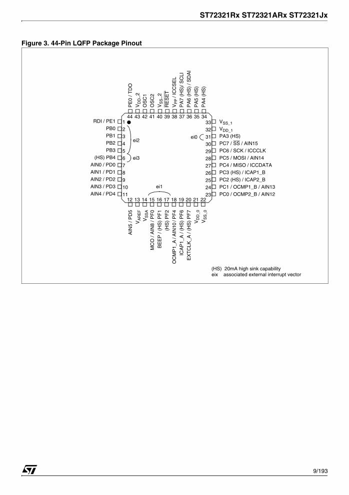
Figure 3. 44-Pin LQFP Package Pinout
MC
O /
AIN
8 / P
F0
BE
EP
/ (H
S)
PF
1
(HS
) P
F2
OC
MP
1_A
/ A
IN10
/ P
F4
ICA
P1_
A /
(HS
) P
F6
EX
TC
LK_A
/ (H
S)
PF
7
VD
D_0
VS
S_0
AIN
5 / P
D5
VA
RE
F
VS
SA
44 43 42 41 40 39 38 37 36 35 3433
32
31
30
29
28
27
26
25
24
2312 13 14 15 16 17 18 19 20 21 22
1
2
3
4
5
6
7
8
9
10
11
ei2
ei3
ei0
ei1
PB3
(HS) PB4
AIN0 / PD0
AIN1 / PD1
AIN2 / PD2
AIN3 / PD3
AIN4 / PD4
RDI / PE1
PB0
PB1
PB2
PC6 / SCK / ICCCLK
PC5 / MOSI / AIN14
PC4 / MISO / ICCDATA
PC3 (HS) / ICAP1_B
PC2 (HS) / ICAP2_B
PC1 / OCMP1_B / AIN13
PC0 / OCMP2_B / AIN12
VSS_1
VDD_1
PA3 (HS)
PC7 / SS / AIN15
VS
S_2
RE
SE
T
VP
P /
ICC
SE
L
PA
7 (H
S)/
SC
LI
PA
6 (H
S)
/ SD
AI
PA
5 (H
S)
PA
4 (H
S)
PE
0 / T
DO
VD
D_2
OS
C1
OS
C2
eix associated external interrupt vector(HS) 20mA high sink capability
9/193

ST72321Rx ST72321ARx ST72321Jx
PIN DESCRIPTION (Cont’d)
For external pin connection guidelines, refer to See “ELECTRICAL CHARACTERISTICS” on page 138.
Legend / Abbreviations for Table 2 :Type: I = input, O = output, S = supply
Input level: A = Dedicated analog input
In/Output level: C = CMOS 0.3VDD/0.7VDDCT= CMOS 0.3VDD/0.7VDD with input triggerTT= TTL 0.8V / 2V with Schmitt trigger
Output level: HS = 20mA high sink (on N-buffer only)
Port and control configuration:
– Input: float = floating, wpu = weak pull-up, int = interrupt 1), ana = analog
– Output: OD = open drain 2), PP = push-pull
Refer to “I/O PORTS” on page 46 for more details on the software configuration of the I/O ports.
The RESET configuration of each pin is shown in bold. This configuration is valid as long as the device isin reset state.
Table 2. Device Pin Description
Pin n°
Pin Name
Typ
e
Level Port Mainfunction
(afterreset)
Alternate function
LQ
FP
64
LQ
FP
44
LQ
FP
32
Inp
ut
Ou
tpu
t Input Output
flo
at
wp
u
int
ana
OD
PP
1 - - PE4 (HS) I/O CT HS X X X X Port E4
2 - - PE5 (HS) I/O CT HS X X X X Port E5
3 - - PE6 (HS) I/O CT HS X X X X Port E6
4 - - PE7 (HS) I/O CT HS X X X X Port E7
5 2 28 PB0/PWM3 I/O CT X ei2 X X Port B0 PWM Output 3
6 3 - PB1/PWM2 I/O CT X ei2 X X Port B1 PWM Output 2
7 4 - PB2/PWM1 I/O CT X ei2 X X Port B2 PWM Output 1
8 5 29 PB3/PWM0 I/O CT X ei2 X X Port B3 PWM Output 0
9 6 30 PB4 (HS)/ARTCLK I/O CT HS X ei3 X X Port B4 PWM-ART External Clock
10 - - PB5 / ARTIC1 I/O CT X ei3 X X Port B5 PWM-ART Input Capture 1
11 - - PB6 / ARTIC2 I/O CT X ei3 X X Port B6 PWM-ART Input Capture 2
12 - - PB7 I/O CT X ei3 X X Port B7
13 7 31 PD0/AIN0 I/O CT X X X X X Port D0 ADC Analog Input 0
14 8 32 PD1/AIN1 I/O CT X X X X X Port D1 ADC Analog Input 1
15 9 - PD2/AIN2 I/O CT X X X X X Port D2 ADC Analog Input 2
16 10 - PD3/AIN3 I/O CT X X X X X Port D3 ADC Analog Input 3
17 11 - PD4/AIN4 I/O CT X X X X X Port D4 ADC Analog Input 4
18 12 - PD5/AIN5 I/O CT X X X X X Port D5 ADC Analog Input 5
19 - - PD6/AIN6 I/O CT X X X X X Port D6 ADC Analog Input 6
20 - - PD7/AIN7 I/O CT X X X X X Port D7 ADC Analog Input 7
21 13 1 VAREF I Analog Reference Voltage for ADC
22 14 2 VSSA S Analog Ground Voltage
10/193

ST72321Rx ST72321ARx ST72321Jx
23 - - VDD_3 S Digital Main Supply Voltage
24 - - VSS_3 S Digital Ground Voltage
25 15 3 PF0/MCO/AIN8 I/O CT X ei1 X X X Port F0Main clock out (fOSC/2)
ADC Ana-logInput 8
26 16 4 PF1 (HS)/BEEP I/O CT HS X ei1 X X Port F1 Beep signal output
27 17 - PF2 (HS) I/O CT HS X ei1 X X Port F2
28 - - PF3/OCMP2_A/AIN9 I/O CT X X X X X Port F3Timer A Out-put Compare 2
ADC Ana-logInput 9
29 18 5PF4/OCMP1_A/AIN10
I/O CT X X X X X Port F4Timer A Out-put Compare 1
ADC Ana-logInput 10
30 - - PF5/ICAP2_A/AIN11 I/O CT X X X X X Port F5Timer A Input Capture 2
ADC Ana-logInput 11
31 19 6 PF6 (HS)/ICAP1_A I/O CT HS X X X X Port F6 Timer A Input Capture 1
32 20 7 PF7 (HS)/EXTCLK_A I/O CT HS X X X X Port F7Timer A External Clock Source
33 21 - VDD_0 S Digital Main Supply Voltage
34 22 - VSS_0 S Digital Ground Voltage
35 23 8PC0/OCMP2_B/AIN12
I/O CT X X X X X Port C0Timer B Out-put Compare 2
ADC Ana-logInput 12
36 24 9PC1/OCMP1_B/AIN13
I/O CT X X X X X Port C1Timer B Out-put Compare 1
ADC Ana-logInput 13
37 25 10 PC2 (HS)/ICAP2_B I/O CT HS X X X X Port C2 Timer B Input Capture 2
38 26 11 PC3 (HS)/ICAP1_B I/O CT HS X X X X Port C3 Timer B Input Capture 1
39 27 12 PC4/MISO/ICCDATA I/O CT X X X X Port C4SPI Master In / Slave Out Data
ICC Data Input
40 28 13 PC5/MOSI/AIN14 I/O CT X X X X X Port C5SPI Master Out / Slave In Data
ADC Ana-logInput 14
41 29 29 PC6/SCK/ICCCLK I/O CT X X X X Port C6
SPI Serial Clock
ICC Clock Output
Caution: Negative cur-rent injection not al-lowed on this pin
42 30 15 PC7/SS/AIN15 I/O CT X X X X X Port C7SPI Slave Se-lect (active low)
ADC Ana-logInput 15
43 - - PA0 I/O CT X ei0 X X Port A0
44 - - PA1 I/O CT X ei0 X X Port A1
Pin n°
Pin Name
Typ
e
Level Port Mainfunction
(afterreset)
Alternate function
LQ
FP
64
LQ
FP
44
LQ
FP
32
Inp
ut
Ou
tpu
t Input Output
flo
at
wp
u
int
ana
OD
PP
11/193

ST72321Rx ST72321ARx ST72321Jx
Notes:1. In the interrupt input column, “eiX” defines the associated external interrupt vector. If the weak pull-upcolumn (wpu) is merged with the interrupt column (int), then the I/O configuration is pull-up interrupt input,else the configuration is floating interrupt input.2. In the open drain output column, “T” defines a true open drain I/O (P-Buffer and protection diode to VDDare not implemented). See See “I/O PORTS” on page 46. and Section 12.8 I/O PORT PIN CHARACTER-
45 - - PA2 I/O CT X ei0 X X Port A2
46 31 16 PA3 (HS) I/O CT HS X ei0 X X Port A3
47 32 - VDD_1 S Digital Main Supply Voltage
48 33 - VSS_1 S Digital Ground Voltage
49 34 17 PA4 (HS) I/O CT HS X X X X Port A4
50 35 - PA5 (HS) I/O CT HS X X X X Port A5
51 36 18 PA6 (HS)/SDAI I/O CT HS X T Port A6 I2C Data 1)
52 37 19 PA7 (HS)/SCLI I/O CT HS X T Port A7 I2C Clock 1)
53 38 20 VPP/ ICCSEL I
Must be tied low. In flash program-ming mode, this pin acts as the pro-gramming voltage input VPP. See Section 12.9.2 for more details. High voltage must not be applied to ROM devices
54 39 21 RESET I/O CT Top priority non maskable interrupt.
55 - - EVD External voltage detector
56 - - TLI I CT X Top level interrupt input pin
57 40 22 VSS_2 S Digital Ground Voltage
58 41 23 OSC23) I/O Resonator oscillator inverter output
59 42 24 OSC13) IExternal clock input or Resonator os-cillator inverter input
60 43 25 VDD_2 S Digital Main Supply Voltage
61 44 26 PE0/TDO I/O CT X X X X Port E0 SCI Transmit Data Out
62 1 27 PE1/RDI I/O CT X X X X Port E1 SCI Receive Data In
63 - -
PE2 (Flash device)
I/O CT
XPort E2
Caution: In Flash devices this port is always input with weak pull-up.
PE2 (ROM device) X X X
Port E2
Caution: In ROM devices, no weak pull-up present on this port.In LQFP44 this pin is not connected to an internal pull-up like other unbond-ed pins (See note 4). It is recommend-ed to configure it as output push pull to avoid added current consumption.
64 - - PE3 I/O CT X X X X Port E3
Pin n°
Pin Name
Typ
e
Level Port Mainfunction
(afterreset)
Alternate function
LQ
FP
64
LQ
FP
44
LQ
FP
32
Inp
ut
Ou
tpu
t Input Output
flo
at
wp
u
int
ana
OD
PP
12/193

ST72321Rx ST72321ARx ST72321Jx
ISTICS for more details.3. OSC1 and OSC2 pins connect a crystal/ceramic resonator, or an external source to the on-chip oscil-lator; see Section 1 DESCRIPTION and Section 12.5 CLOCK AND TIMING CHARACTERISTICS formore details.4. On the chip, each I/O port may have up to 8 pads:
– ads that are not bonded to external pins are forced by hardware in input pull-up configuration after reset. The configuration of these pads must be kept at reset state to avoid added current consumption.
5. Pull-up always activated on PE2 see limitation Section 15.4.6.6. It is mandatory to connect all available VDD and VREF pins to the supply voltage and all VSS and VSSApins to ground.
13/193

ST72321Rx ST72321ARx ST72321Jx
3 REGISTER & MEMORY MAPAs shown in Figure 4, the MCU is capable of ad-dressing 64K bytes of memories and I/O registers.
The available memory locations consist of 128bytes of register locations, up to 2Kbytes of RAMand up to 60Kbytes of user program memory. TheRAM space includes up to 256 bytes for the stackfrom 0100h to 01FFh.
The highest address bytes contain the user resetand interrupt vectors.
IMPORTANT: Memory locations marked as “Re-served” must never be accessed. Accessing a re-seved area can have unpredictable effects on thedevice.
Related DocumentationAN 985: Executing Code in ST7 RAM
Figure 4. Memory Map
0000h
RAM
Program Memory(60K, 48K or 32K)
Interrupt & Reset Vectors
HW Registers
0080h007Fh
0FFFh
(see Table 3)
1000h
FFDFhFFE0h
FFFFh(see Table 8)
0880hReserved
087Fh
Short AddressingRAM (zero page)
256 Bytes Stack
16-bit AddressingRAM
0100h
01FFh
0080h
0200h
00FFh
or 087Fh32 KBytes
8000h
60 KBytes
48 KBytes
FFFFh
1000h
4000h
(2048, 1536 or 1024 Bytes)
or 067Fhor 047Fh
14/193

ST72321Rx ST72321ARx ST72321Jx
Table 3. Hardware Register Map
Address BlockRegister
LabelRegister Name
Reset Status
Remarks
0000h0001h0002h
Port A 2)PADRPADDRPAOR
Port A Data RegisterPort A Data Direction RegisterPort A Option Register
00h1)
00h00h
R/WR/WR/W
0003h0004h0005h
Port B 2)PBDRPBDDRPBOR
Port B Data RegisterPort B Data Direction RegisterPort B Option Register
00h1)
00h00h
R/WR/WR/W
0006h0007h0008h
Port CPCDRPCDDRPCOR
Port C Data RegisterPort C Data Direction RegisterPort C Option Register
00h1)
00h00h
R/WR/WR/W
0009h000Ah000Bh
Port D 2)PDDRPDDDRPDOR
Port D Data RegisterPort D Data Direction RegisterPort D Option Register
00h1)
00h00h
R/WR/WR/W
000Ch000Dh000Eh
Port E 2)PEDRPEDDRPEOR
Port E Data RegisterPort E Data Direction RegisterPort E Option Register
00h1)
00h00h
R/WR/W2)
R/W2)
000Fh0010h0011h
Port F 2)PFDRPFDDRPFOR
Port F Data RegisterPort F Data Direction RegisterPort F Option Register
00h1)
00h00h
R/WR/WR/W
0012hto
0017hReserved Area (6 Bytes)
0018h0019h001Ah001Bh001Ch001Dh001Eh
I2C
I2CCRI2CSR1I2CSR2I2CCCRI2COAR1I2COAR2I2CDR
I2C Control RegisterI2C Status Register 1I2C Status Register 2I2C Clock Control RegisterI2C Own Address Register 1I2C Own Address Register2I2C Data Register
00h00h00h00h00h00h00h
R/W Read Only Read Only R/W R/W R/W R/W
001Fh0020h
Reserved Area (2 Bytes)
0021h0022h0023h
SPISPIDRSPICRSPICSR
SPI Data I/O RegisterSPI Control RegisterSPI Control/Status Register
xxh0xh00h
R/W R/W R/W
0024h0025h0026h0027h
ITC
ISPR0ISPR1ISPR2ISPR3
Interrupt Software Priority Register 0Interrupt Software Priority Register 1Interrupt Software Priority Register 2Interrupt Software Priority Register 3
FFhFFhFFhFFh
R/WR/WR/WR/W
0028h EICR External Interrupt Control Register 00h R/W
0029h FLASH FCSR Flash Control/Status Register 00h R/W
15/193

ST72321Rx ST72321ARx ST72321Jx
002Ah WATCHDOG WDGCR Watchdog Control Register 7Fh R/W
002Bh SICSR System Integrity Control/Status Register 000x 000x b R/W
002Ch002Dh
MCCMCCSRMCCBCR
Main Clock Control / Status RegisterMain Clock Controller: Beep Control Register
00h00h
R/WR/W
002Ehto
0030hReserved Area (3 Bytes)
0031h0032h0033h0034h0035h0036h0037h0038h0039h003Ah003Bh003Ch003Dh003Eh003Fh
TIMER A
TACR2TACR1TACSRTAIC1HRTAIC1LRTAOC1HRTAOC1LRTACHRTACLRTAACHRTAACLRTAIC2HRTAIC2LRTAOC2HRTAOC2LR
Timer A Control Register 2Timer A Control Register 1Timer A Control/Status RegisterTimer A Input Capture 1 High RegisterTimer A Input Capture 1 Low RegisterTimer A Output Compare 1 High RegisterTimer A Output Compare 1 Low RegisterTimer A Counter High RegisterTimer A Counter Low RegisterTimer A Alternate Counter High RegisterTimer A Alternate Counter Low RegisterTimer A Input Capture 2 High RegisterTimer A Input Capture 2 Low RegisterTimer A Output Compare 2 High RegisterTimer A Output Compare 2 Low Register
00h00h
xxxx x0xx bxxhxxh80h00hFFhFChFFhFChxxhxxh80h00h
R/W R/W R/W Read Only Read Only R/W R/W Read Only Read Only Read Only Read Only Read Only Read Only R/W R/W
0040h Reserved Area (1 Byte)
0041h0042h0043h0044h0045h0046h0047h0048h0049h004Ah004Bh004Ch004Dh004Eh004Fh
TIMER B
TBCR2TBCR1TBCSRTBIC1HRTBIC1LRTBOC1HRTBOC1LRTBCHRTBCLRTBACHRTBACLRTBIC2HRTBIC2LRTBOC2HRTBOC2LR
Timer B Control Register 2Timer B Control Register 1Timer B Control/Status RegisterTimer B Input Capture 1 High RegisterTimer B Input Capture 1 Low RegisterTimer B Output Compare 1 High RegisterTimer B Output Compare 1 Low RegisterTimer B Counter High RegisterTimer B Counter Low RegisterTimer B Alternate Counter High RegisterTimer B Alternate Counter Low RegisterTimer B Input Capture 2 High RegisterTimer B Input Capture 2 Low RegisterTimer B Output Compare 2 High RegisterTimer B Output Compare 2 Low Register
00h00h
xxxx x0xx bxxhxxh80h00hFFhFChFFhFChxxhxxh80h00h
R/W R/W R/W Read Only Read Only R/W R/W Read Only Read Only Read Only Read Only Read Only Read Only R/W R/W
0050h0051h0052h0053h0054h0055h0056h0057h
SCI
SCISRSCIDRSCIBRRSCICR1SCICR2SCIERPR
SCIETPR
SCI Status RegisterSCI Data RegisterSCI Baud Rate RegisterSCI Control Register 1SCI Control Register 2SCI Extended Receive Prescaler RegisterReserved areaSCI Extended Transmit Prescaler Register
C0hxxh00h
x000 0000b00h00h---
00h
Read Only R/W R/W R/W R/W R/W
R/W
Address BlockRegister
LabelRegister Name
Reset Status
Remarks
16/193

ST72321Rx ST72321ARx ST72321Jx
Legend: x=undefined, R/W=read/write
Notes:1. The contents of the I/O port DR registers are readable only in output configuration. In input configura-tion, the values of the I/O pins are returned instead of the DR register contents.2. The bits associated with unavailable pins must always keep their reset value.
0058hto
006FhReserved Area (24 Bytes)
0070h0071h0072h
ADCADCCSRADCDRHADCDRL
Control/Status RegisterData High RegisterData Low Register
00h00h00h
R/WRead Only Read Only
0073h0074h0075h0076h0077h
0078h0079h007Ah
007Bh007Ch007Dh
PWM ART
PWMDCR3PWMDCR2PWMDCR1PWMDCR0PWMCRARTCSRARTCARARTARRARTICCSRARTICR1ARTICR2
PWM AR Timer Duty Cycle Register 3PWM AR Timer Duty Cycle Register 2PWM AR Timer Duty Cycle Register 1PWM AR Timer Duty Cycle Register 0PWM AR Timer Control RegisterAuto-Reload Timer Control/Status RegisterAuto-Reload Timer Counter Access RegisterAuto-Reload Timer Auto-Reload RegisterAR Timer Input Capture Control/Status Reg.AR Timer Input Capture Register 1AR Timer Input Capture Register 1
00h00h00h00h00h00h00h00h
00h00h00h
R/WR/WR/WR/WR/WR/WR/WR/WR/WRead OnlyRead Only
007Eh007Fh
Reserved Area (2 Bytes)
Address BlockRegister
LabelRegister Name
Reset Status
Remarks
17/193

ST72321Rx ST72321ARx ST72321Jx
4 FLASH PROGRAM MEMORY
4.1 Introduction
The ST7 dual voltage High Density Flash (HDFlash) is a non-volatile memory that can beelectrically erased as a single block or by individu-al sectors and programmed on a Byte-by-Byte ba-sis using an external VPP supply.
The HDFlash devices can be programmed anderased off-board (plugged in a programming tool)or on-board using ICP (In-Circuit Programming) orIAP (In-Application Programming).
The array matrix organisation allows each sectorto be erased and reprogrammed without affectingother sectors.
4.2 Main Features
■ Three Flash programming modes:– Insertion in a programming tool. In this mode,
all sectors including option bytes can be pro-grammed or erased.
– ICP (In-Circuit Programming). In this mode, allsectors including option bytes can be pro-grammed or erased without removing the de-vice from the application board.
– IAP (In-Application Programming) In thismode, all sectors except Sector 0, can be pro-grammed or erased without removing the de-vice from the application board and while theapplication is running.
■ ICT (In-Circuit Testing) for downloading andexecuting user application test patterns in RAM
■ Read-out protection■ Register Access Security System (RASS) to
prevent accidental programming or erasing
4.3 Structure
The Flash memory is organised in sectors and canbe used for both code and data storage.
Depending on the overall Flash memory size in themicrocontroller device, there are up to three user
sectors (see Table 4). Each of these sectors canbe erased independently to avoid unnecessaryerasing of the whole Flash memory when only apartial erasing is required.
The first two sectors have a fixed size of 4 Kbytes(see Figure 5). They are mapped in the upper partof the ST7 addressing space so the reset and in-terrupt vectors are located in Sector 0 (F000h-FFFFh).
Table 4. Sectors available in Flash devices
4.3.1 Read-out ProtectionRead-out protection, when selected, provides aprotection against Program Memory content ex-traction and against write access to Flash memo-ry. Even if no protection can be considered as to-tally unbreakable, the feature provides a very highlevel of protection for a general purpose microcon-troller.
In flash devices, this protection is removed by re-programming the option. In this case, the entireprogram memory is first automatically erased andthe device can be reprogrammed.
Read-out protection selection depends on the de-vice type:
– In Flash devices it is enabled and removed through the FMP_R bit in the option byte.
– In ROM devices it is enabled by mask option specified in the Option List.
Note: In flash devices, the LVD is not supported ifread-out protection is enabled.
Figure 5. Memory Map and Sector Address
Flash Size (bytes) Available Sectors
4K Sector 0
8K Sectors 0,1
> 8K Sectors 0,1, 2
4 Kbytes
4 Kbytes
2 Kbytes
SECTOR 1
SECTOR 0
16 Kbytes
SECTOR 2
8K 16K 32K 60K FLASH
FFFFh
EFFFh
DFFFh
3FFFh
7FFFh
1000h
24 Kbytes
MEMORY SIZE
8 Kbytes 40 Kbytes 52 Kbytes
9FFFh
BFFFh
D7FFh
4K 10K 24K 48K
18/193

ST72321Rx ST72321ARx ST72321Jx
FLASH PROGRAM MEMORY (Cont’d)
4.4 ICC Interface
ICC needs a minimum of 4 and up to 6 pins to beconnected to the programming tool (see Figure 6).These pins are:
– RESET: device reset– VSS: device power supply ground
– ICCCLK: ICC output serial clock pin– ICCDATA: ICC input/output serial data pin– ICCSEL/VPP: programming voltage– OSC1(or OSCIN): main clock input for exter-
nal source (optional)– VDD: application board power supply (option-
al, see Figure 6, Note 3)
Figure 6. Typical ICC Interface
Notes:1. If the ICCCLK or ICCDATA pins are only usedas outputs in the application, no signal isolation isnecessary. As soon as the Programming Tool isplugged to the board, even if an ICC session is notin progress, the ICCCLK and ICCDATA pins arenot available for the application. If they are used asinputs by the application, isolation such as a serialresistor has to implemented in case another de-vice forces the signal. Refer to the ProgrammingTool documentation for recommended resistor val-ues.
2. During the ICC session, the programming toolmust control the RESET pin. This can lead to con-flicts between the programming tool and the appli-cation reset circuit if it drives more than 5mA athigh level (push pull output or pull-up resistor<1K).A schottky diode can be used to isolate the appli-cation RESET circuit in this case. When using aclassical RC network with R>1K or a reset man-
agement IC with open drain output and pull-up re-sistor>1K, no additional components are needed.In all cases the user must ensure that no externalreset is generated by the application during theICC session.
3. The use of Pin 7 of the ICC connector dependson the Programming Tool architecture. This pinmust be connected when using most ST Program-ming Tools (it is used to monitor the applicationpower supply). Please refer to the ProgrammingTool manual.
4. Pin 9 has to be connected to the OSC1 or OS-CIN pin of the ST7 when the clock is not availablein the application or if the selected clock option isnot programmed in the option byte. ST7 deviceswith multi-oscillator capability need to have OSC2grounded in this case.
ICC CONNECTOR
ICC
DA
TA
ICC
CLK
RE
SE
T
VD
D
HE10 CONNECTOR TYPE
APPLICATIONPOWER SUPPLY
1
246810
9 7 5 3
PROGRAMMING TOOL
ICC CONNECTOR
APPLICATION BOARD ICC Cable
(See Note 3)
10kΩ
VS
S
ICC
SE
L/V
PP
ST7
CL2 CL1
OS
C1
OS
C2
OPTIONAL
See Note 1
See Note 2
APPLICATIONRESET SOURCE
APPLICATIONI/O
(See Note 4)
19/193

ST72321Rx ST72321ARx ST72321Jx
FLASH PROGRAM MEMORY (Cont’d)
4.5 ICP (In-Circuit Programming)
To perform ICP the microcontroller must beswitched to ICC (In-Circuit Communication) modeby an external controller or programming tool.
Depending on the ICP code downloaded in RAM,Flash memory programming can be fully custom-ized (number of bytes to program, program loca-tions, or selection serial communication interfacefor downloading).
When using an STMicroelectronics or third-partyprogramming tool that supports ICP and the spe-cific microcontroller device, the user needs only toimplement the ICP hardware interface on the ap-plication board (see Figure 6). For more details onthe pin locations, refer to the device pinout de-scription.
4.6 IAP (In-Application Programming)
This mode uses a BootLoader program previouslystored in Sector 0 by the user (in ICP mode or byplugging the device in a programming tool).
This mode is fully controlled by user software. Thisallows it to be adapted to the user application, (us-er-defined strategy for entering programmingmode, choice of communications protocol used tofetch the data to be stored, etc.). For example, it is
possible to download code from the SPI, SCI, USBor CAN interface and program it in the Flash. IAPmode can be used to program any of the Flashsectors except Sector 0, which is write/erase pro-tected to allow recovery in case errors occur dur-ing the programming operation.
4.7 Related Documentation
For details on Flash programming and ICC proto-col, refer to the ST7 Flash Programming Refer-ence Manual and to the ST7 ICC Protocol Refer-ence Manual.4.7.1 Register DescriptionFLASH CONTROL/STATUS REGISTER (FCSR)
Read/Write
Reset Value: 0000 0000 (00h)
This register is reserved for use by ProgrammingTool software. It controls the Flash programmingand erasing operations.
Figure 7. Flash Control/Status Register Address and Reset Value
7 0
0 0 0 0 0 0 0 0
Address(Hex.)
RegisterLabel
7 6 5 4 3 2 1 0
0029hFCSRReset Value 0 0 0 0 0 0 0 0
20/193

ST72321Rx ST72321ARx ST72321Jx
5 CENTRAL PROCESSING UNIT
5.1 INTRODUCTION
This CPU has a full 8-bit architecture and containssix internal registers allowing efficient 8-bit datamanipulation.
5.2 MAIN FEATURES
■ Enable executing 63 basic instructions■ Fast 8-bit by 8-bit multiply■ 17 main addressing modes (with indirect
addressing mode)■ Two 8-bit index registers■ 16-bit stack pointer■ Low power HALT and WAIT modes■ Priority maskable hardware interrupts■ Non-maskable software/hardware interrupts
5.3 CPU REGISTERS
The six CPU registers shown in Figure 1 are notpresent in the memory mapping and are accessedby specific instructions.
Accumulator (A)The Accumulator is an 8-bit general purpose reg-ister used to hold operands and the results of thearithmetic and logic calculations and to manipulatedata.
Index Registers (X and Y)These 8-bit registers are used to create effectiveaddresses or as temporary storage areas for datamanipulation. (The Cross-Assembler generates aprecede instruction (PRE) to indicate that the fol-lowing instruction refers to the Y register.)
The Y register is not affected by the interrupt auto-matic procedures.
Program Counter (PC) The program counter is a 16-bit register containingthe address of the next instruction to be executedby the CPU. It is made of two 8-bit registers PCL(Program Counter Low which is the LSB) and PCH(Program Counter High which is the MSB).
Figure 8. CPU Registers
ACCUMULATOR
X INDEX REGISTER
Y INDEX REGISTER
STACK POINTER
CONDITION CODE REGISTER
PROGRAM COUNTER
7 0
1 C1 I1 H I0 N Z
RESET VALUE = RESET VECTOR @ FFFEh-FFFFh
7 0
7 0
7 0
0715 8PCH PCL
15 8 7 0
RESET VALUE = STACK HIGHER ADDRESS
RESET VALUE = 1 X1 1 X 1 X X
RESET VALUE = XXh
RESET VALUE = XXh
RESET VALUE = XXh
X = Undefined Value
21/193

ST72321Rx ST72321ARx ST72321Jx
CENTRAL PROCESSING UNIT (Cont’d)
Condition Code Register (CC) Read/Write
Reset Value: 111x1xxx
The 8-bit Condition Code register contains the in-terrupt masks and four flags representative of theresult of the instruction just executed. This registercan also be handled by the PUSH and POP in-structions.
These bits can be individually tested and/or con-trolled by specific instructions.
Arithmetic Management Bits
Bit 4 = H Half carry.
This bit is set by hardware when a carry occurs be-tween bits 3 and 4 of the ALU during an ADD orADC instructions. It is reset by hardware duringthe same instructions.
0: No half carry has occurred.1: A half carry has occurred.
This bit is tested using the JRH or JRNH instruc-tion. The H bit is useful in BCD arithmetic subrou-tines.
Bit 2 = N Negative.
This bit is set and cleared by hardware. It is repre-sentative of the result sign of the last arithmetic,logical or data manipulation. It’s a copy of the re-sult 7th bit.0: The result of the last operation is positive or null.1: The result of the last operation is negative
(that is, the most significant bit is a logic 1).
This bit is accessed by the JRMI and JRPL instruc-tions.
Bit 1 = Z Zero.
This bit is set and cleared by hardware. This bit in-dicates that the result of the last arithmetic, logicalor data manipulation is zero.0: The result of the last operation is different from
zero.1: The result of the last operation is zero.
This bit is accessed by the JREQ and JRNE testinstructions.
Bit 0 = C Carry/borrow.This bit is set and cleared by hardware and soft-ware. It indicates an overflow or an underflow hasoccurred during the last arithmetic operation.0: No overflow or underflow has occurred.1: An overflow or underflow has occurred.
This bit is driven by the SCF and RCF instructionsand tested by the JRC and JRNC instructions. It isalso affected by the “bit test and branch”, shift androtate instructions.
Interrupt Management Bits
Bit 5,3 = I1, I0 Interrupt
The combination of the I1 and I0 bits gives the cur-rent interrupt software priority.
These two bits are set/cleared by hardware whenentering in interrupt. The loaded value is given bythe corresponding bits in the interrupt software pri-ority registers (IxSPR). They can be also set/cleared by software with the RIM, SIM, IRET,HALT, WFI and PUSH/POP instructions.
See the interrupt management chapter for moredetails.
7 0
1 1 I1 H I0 N Z C
Interrupt Software Priority I1 I0Level 0 (main) 1 0Level 1 0 1Level 2 0 0Level 3 (= interrupt disable) 1 1
22/193

ST72321Rx ST72321ARx ST72321Jx
CENTRAL PROCESSING UNIT (Cont’d)
Stack Pointer (SP)Read/Write
Reset Value: 01 FFh
The Stack Pointer is a 16-bit register which is al-ways pointing to the next free location in the stack.It is then decremented after data has been pushedonto the stack and incremented before data ispopped from the stack (see Figure 2).
Since the stack is 256 bytes deep, the 8 most sig-nificant bits are forced by hardware. Following anMCU Reset, or after a Reset Stack Pointer instruc-tion (RSP), the Stack Pointer contains its reset val-ue (the SP7 to SP0 bits are set) which is the stackhigher address.
The least significant byte of the Stack Pointer(called S) can be directly accessed by a LD in-struction.
Note: When the lower limit is exceeded, the StackPointer wraps around to the stack upper limit, with-out indicating the stack overflow. The previouslystored information is then overwritten and there-fore lost. The stack also wraps in case of an under-flow.
The stack is used to save the return address dur-ing a subroutine call and the CPU context duringan interrupt. The user may also directly manipulatethe stack by means of the PUSH and POP instruc-tions. In the case of an interrupt, the PCL is storedat the first location pointed to by the SP. Then theother registers are stored in the next locations asshown in Figure 2.
– When an interrupt is received, the SP is decre-mented and the context is pushed on the stack.
– On return from interrupt, the SP is incremented and the context is popped from the stack.
A subroutine call occupies two locations and an in-terrupt five locations in the stack area.
Figure 9. Stack Manipulation Example
15 8
0 0 0 0 0 0 0 1
7 0
SP7 SP6 SP5 SP4 SP3 SP2 SP1 SP0
PCH
PCL
SP
PCH
PCL
SP
PCL
PCH
X
ACC
PCH
PCL
SP
PCL
PCH
X
ACC
PCH
PCL
SP
PCL
PCH
X
ACC
PCH
PCL
SP
SP
Y
CALLSubroutine
Interrupt Event
PUSH Y POP Y IRET RETor RSP
@ 01FFh
@ 0100h
Stack Higher Address = 01FFhStack Lower Address = 0100h
23/193

ST72321Rx ST72321ARx ST72321Jx
6 SUPPLY, RESET AND CLOCK MANAGEMENTThe device includes a range of utility features forsecuring the application in critical situations (forexample in case of a power brown-out), and re-ducing the number of external components. Anoverview is shown in Figure 11.
For more details, refer to dedicated parametricsection.
Main features■ Optional PLL for multiplying the frequency by 2
(not to be used with internal RC oscillator)■ Reset Sequence Manager (RSM)■ Multi-Oscillator Clock Management (MO)
– 5 Crystal/Ceramic resonator oscillators– 1 Internal RC oscillator
■ System Integrity Management (SI)
– Main supply Low voltage detection (LVD)– Auxiliary Voltage detector (AVD) with interrupt
capability for monitoring the main supply orthe EVD pin
6.1 PHASE LOCKED LOOP
If the clock frequency input to the PLL is in therange 2 to 4 MHz, the PLL can be used to multiplythe frequency by two to obtain an fOSC2 of 4 to 8MHz. The PLL is enabled by option byte. If the PLLis disabled, then fOSC2 = fOSC/2.
Caution: The PLL is not recommended for appli-cations where timing accuracy is required. See“PLL Characteristics” on page 151.
Figure 10. PLL Block Diagram
Figure 11. Clock, Reset and Supply Block Diagram
0
1
PLL OPTION BIT
PLL x 2fOSC2
/ 2
fOSC
LOW VOLTAGE
DETECTOR
(LVD)
fOSC2
AUXILIARY VOLTAGE
DETECTOR
(AVD)
MULTI-
OSCILLATOR
(MO)OSC1
RESET
VSS
EVD
VDD
RESET SEQUENCE
MANAGER
(RSM)
OSC2 MAIN CLOCK
AVD Interrupt Request
CONTROLLERPLL
SYSTEM INTEGRITY MANAGEMENT
WATCHDOG
SICSR TIMER (WDG)
WITH REALTIME CLOCK (MCC/RTC)
AVD AVD AVD LVDRFIE
WDGRF
0
1
fOSC
(option)
0S F
fCPU
0 0
24/193

ST72321Rx ST72321ARx ST72321Jx
6.2 MULTI-OSCILLATOR (MO)
The main clock of the ST7 can be generated bythree different source types coming from the multi-oscillator block:■ an external source■ 4 crystal or ceramic resonator oscillators■ an internal high frequency RC oscillator
Each oscillator is optimized for a given frequencyrange in terms of consumption and is selectablethrough the option byte. The associated hardwareconfigurations are shown in Table 5. Refer to theelectrical characteristics section for more details.
Caution: The OSC1 and/or OSC2 pins must notbe left unconnected. For the purposes of FailureMode and Effect Analysis, it should be noted that ifthe OSC1 and/or OSC2 pins are left unconnected,the ST7 main oscillator may start and, in this con-figuration, could generate an fOSC clock frequencyin excess of the allowed maximum (>16MHz.),putting the ST7 in an unsafe/undefined state. Theproduct behaviour must therefore be consideredundefined when the OSC pins are left unconnect-ed.
External Clock SourceIn this external clock mode, a clock signal (square,sinus or triangle) with ~50% duty cycle has to drivethe OSC1 pin while the OSC2 pin is tied to ground.
Crystal/Ceramic OscillatorsThis family of oscillators has the advantage of pro-ducing a very accurate rate on the main clock ofthe ST7. The selection within a list of 4 oscillatorswith different frequency ranges has to be done byoption byte in order to reduce consumption (referto section 14.1 on page 175 for more details on thefrequency ranges). In this mode of the multi-oscil-lator, the resonator and the load capacitors haveto be placed as close as possible to the oscillatorpins in order to minimize output distortion andstart-up stabilization time. The loading capaci-tance values must be adjusted according to theselected oscillator.
These oscillators are not stopped during theRESET phase to avoid losing time in the oscillatorstart-up phase.
Internal RC OscillatorThis oscillator allows a low cost solution for themain clock of the ST7 using only an internal resis-tor and capacitor. Internal RC oscillator mode hasthe drawback of a lower frequency accuracy andshould not be used in applications that require ac-curate timing.
In this mode, the two oscillator pins have to be tiedto ground.
Table 5. ST7 Clock Sources
Hardware Configuration
Ext
erna
lClo
ckC
ryst
al/C
eram
icR
eson
ator
sIn
tern
alR
CO
scill
ator
OSC1 OSC2
EXTERNAL
ST7
SOURCE
OSC1 OSC2
LOADCAPACITORS
ST7
CL2CL1
OSC1 OSC2ST7
25/193

ST72321Rx ST72321ARx ST72321Jx
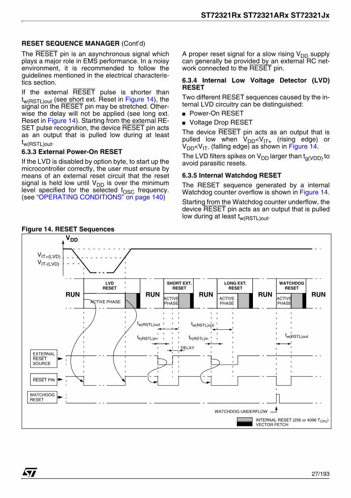
6.3 RESET SEQUENCE MANAGER (RSM)
6.3.1 IntroductionThe reset sequence manager includes three RE-SET sources as shown in Figure 13:■ External RESET source pulse■ Internal LVD RESET (Low Voltage Detection)■ Internal WATCHDOG RESET
These sources act on the RESET pin and it is al-ways kept low during the delay phase.
The RESET service routine vector is fixed at ad-dresses FFFEh-FFFFh in the ST7 memory map.
The basic RESET sequence consists of 3 phasesas shown in Figure 12:■ Active Phase depending on the RESET source■ 256 or 4096 CPU clock cycle delay (selected by
option byte)■ RESET vector fetch
The 256 or 4096 CPU clock cycle delay allows theoscillator to stabilise and ensures that recoveryhas taken place from the Reset state. The shorteror longer clock cycle delay should be selected byoption byte to correspond to the stabilization timeof the external oscillator used in the application(see section 14.1 on page 175).
The RESET vector fetch phase duration is 2 clockcycles.
Figure 12. RESET Sequence Phases
Caution: When the ST7 is unprogrammed or fullyerased, the Flash is blank and the RESET vectoris not programmed.
For this reason, it is recommended to keep theRESET pin in low state until programming mode isentered, in order to avoid unwanted behavior.
6.3.2 Asynchronous External RESET pinThe RESET pin is both an input and an open-drainoutput with integrated RON weak pull-up resistor.This pull-up has no fixed value but varies in ac-cordance with the input voltage. It can be pulledlow by external circuitry to reset the device. See“CONTROL PIN CHARACTERISTICS” onpage 159 for more details.
A RESET signal originating from an externalsource must have a duration of at least th(RSTL)in inorder to be recognized (see Figure 14). This de-tection is asynchronous and therefore the MCUcan enter reset state even in HALT mode.
Figure 13. Reset Block Diagram
RESET
Active PhaseINTERNAL RESET
256 or 4096 CLOCK CYCLESFETCH
VECTOR
RESET
RON
VDD
WATCHDOG RESET
LVD RESET
INTERNALRESET
PULSEGENERATOR
Filter
26/193
ST72321Rx ST72321ARx ST72321Jx
RESET SEQUENCE MANAGER (Cont’d)
The RESET pin is an asynchronous signal whichplays a major role in EMS performance. In a noisyenvironment, it is recommended to follow theguidelines mentioned in the electrical characteris-tics section.
If the external RESET pulse is shorter thantw(RSTL)out (see short ext. Reset in Figure 14), thesignal on the RESET pin may be stretched. Other-wise the delay will not be applied (see long ext.Reset in Figure 14). Starting from the external RE-SET pulse recognition, the device RESET pin actsas an output that is pulled low during at leasttw(RSTL)out.
6.3.3 External Power-On RESETIf the LVD is disabled by option byte, to start up themicrocontroller correctly, the user must ensure bymeans of an external reset circuit that the resetsignal is held low until VDD is over the minimumlevel specified for the selected fOSC frequency.(see “OPERATING CONDITIONS” on page 140)
A proper reset signal for a slow rising VDD supplycan generally be provided by an external RC net-work connected to the RESET pin.
6.3.4 Internal Low Voltage Detector (LVD)RESETTwo different RESET sequences caused by the in-ternal LVD circuitry can be distinguished:■ Power-On RESET■ Voltage Drop RESET
The device RESET pin acts as an output that ispulled low when VDD<VIT+ (rising edge) orVDD<VIT- (falling edge) as shown in Figure 14.
The LVD filters spikes on VDD larger than tg(VDD) toavoid parasitic resets.
6.3.5 Internal Watchdog RESETThe RESET sequence generated by a internalWatchdog counter overflow is shown in Figure 14.
Starting from the Watchdog counter underflow, thedevice RESET pin acts as an output that is pulledlow during at least tw(RSTL)out.
Figure 14. RESET Sequences VDD
RUN
RESET PIN
EXTERNAL
WATCHDOG
ACTIVE PHASE
VIT+(LVD)VIT-(LVD)
th(RSTL)in
tw(RSTL)out
RUN
th(RSTL)in
ACTIVE
WATCHDOG UNDERFLOW
tw(RSTL)out
RUN RUN RUN
RESET
RESETSOURCE
SHORT EXT.RESET
LVDRESET
LONG EXT.RESET
WATCHDOGRESET
INTERNAL RESET (256 or 4096 TCPU)VECTOR FETCH
tw(RSTL)out
PHASEACTIVEPHASE
ACTIVEPHASE
DELAY
27/193

ST72321Rx ST72321ARx ST72321Jx
6.4 SYSTEM INTEGRITY MANAGEMENT (SI)
The System Integrity Management block containsthe Low Voltage Detector (LVD), Auxiliary Volt-age Detector (AVD) functions. It is managed bythe SICSR register.
6.4.1 Low Voltage Detector (LVD)The Low Voltage Detector function (LVD) gener-ates a static reset when the VDD supply voltage isbelow a VIT- reference value. This means that itsecures the power-up as well as the power-downkeeping the ST7 in reset.
The VIT- reference value for a voltage drop is lowerthan the VIT+ reference value for power-on in orderto avoid a parasitic reset when the MCU starts run-ning and sinks current on the supply (hysteresis).
The LVD Reset circuitry generates a reset whenVDD is below:
– VIT+ when VDD is rising – VIT- when VDD is falling
The LVD function is illustrated in Figure 15.
The voltage threshold can be configured by optionbyte to be low, medium or high.
Provided the minimum VDD value (guaranteed forthe oscillator frequency) is above VIT-, the MCUcan only be in two modes:
– under full software control– in static safe reset
In these conditions, secure operation is always en-sured for the application without the need for ex-ternal reset hardware.
During a Low Voltage Detector Reset, the RESETpin is held low, thus permitting the MCU to resetother devices.
Notes:
The LVD allows the device to be used without anyexternal RESET circuitry.
If the medium or low thresholds are selected, thedetection may occur outside the specified operat-ing voltage range. Below 3.8V, device operation isnot guaranteed.
The LVD is an optional function which can be se-lected by option byte.
It is recommended to make sure that the VDD sup-ply voltage rises monotonously when the device isexiting from Reset, to ensure the application func-tions properly.
Figure 15. Low Voltage Detector vs Reset
VDD
VIT+
RESET
VIT-
Vhys
28/193

ST72321Rx ST72321ARx ST72321Jx
SYSTEM INTEGRITY MANAGEMENT (Cont’d)
6.4.2 Auxiliary Voltage Detector (AVD)The Voltage Detector function (AVD) is based onan analog comparison between a VIT-(AVD) andVIT+(AVD) reference value and the VDD main sup-ply or the external EVD pin voltage level (VEVD).The VIT- reference value for falling voltage is lowerthan the VIT+ reference value for rising voltage inorder to avoid parasitic detection (hysteresis).
The output of the AVD comparator is directly read-able by the application software through a realtime status bit (AVDF) in the SICSR register. Thisbit is read only.Caution: The AVD function is active only if theLVD is enabled through the option byte.6.4.2.1 Monitoring the VDD Main SupplyThis mode is selected by clearing the AVDS bit inthe SICSR register.
The AVD voltage threshold value is relative to theselected LVD threshold configured by option byte(see section 14.1 on page 175).
If the AVD interrupt is enabled, an interrupt is gen-erated when the voltage crosses the VIT+(AVD) orVIT-(AVD) threshold (AVDF bit toggles).
In the case of a drop in voltage, the AVD interruptacts as an early warning, allowing software to shutdown safely before the LVD resets the microcon-troller. See Figure 16.
The interrupt on the rising edge is used to informthe application that the VDD warning state is over.
If the voltage rise time trv is less than 256 or 4096CPU cycles (depending on the reset delay select-ed by option byte), no AVD interrupt will be gener-ated when VIT+(AVD) is reached.
If trv is greater than 256 or 4096 cycles then:
– If the AVD interrupt is enabled before the VIT+(AVD) threshold is reached, then 2 AVD inter-rupts will be received: the first when the AVDIE bit is set, and the second when the threshold is reached.
– If the AVD interrupt is enabled after the VIT+(AVD) threshold is reached then only one AVD interrupt will occur.
Figure 16. Using the AVD to Monitor VDD (AVDS bit=0)
VDD
VIT+(AVD)
VIT-(AVD)
AVDF bit 0 0RESET VALUE
IF AVDIE bit = 1
Vhyst
AVD INTERRUPTREQUEST
INTERRUPT PROCESS INTERRUPT PROCESS
VIT+(LVD)
VIT-(LVD)
LVD RESET
Early Warning Interrupt(Power has dropped, MCU not not yet in reset)
11
trv VOLTAGE RISE TIME
29/193

ST72321Rx ST72321ARx ST72321Jx
SYSTEM INTEGRITY MANAGEMENT (Cont’d)
6.4.2.2 Monitoring a Voltage on the EVD pinThis mode is selected by setting the AVDS bit inthe SICSR register.
The AVD circuitry can generate an interrupt whenthe AVDIE bit of the SICSR register is set. This in-terrupt is generated on the rising and falling edges
of the comparator output. This means it is generat-ed when either one of these two events occur:
– VEVD rises up to VIT+(EVD)– VEVD falls down to VIT-(EVD)
The EVD function is illustrated in Figure 17.
For more details, refer to the Electrical Character-istics section.
Figure 17. Using the Voltage Detector to Monitor the EVD pin (AVDS bit=1)
6.4.3 Low Power Modes
6.4.3.1 InterruptsThe AVD interrupt event generate an interrupt ifthe corresponding Enable Control Bit (AVDIE) is
set and the interrupt mask in the CC register is re-set (RIM instruction).
VEVD
VIT+(EVD)
VIT-(EVD)
AVDF 0 01
IF AVDIE = 1
Vhyst
AVD INTERRUPTREQUEST
INTERRUPT PROCESS INTERRUPT PROCESS
Mode Description
WAITNo effect on SI. AVD interrupts cause the device to exit from Wait mode.
HALT The SICSR register is frozen.
Interrupt EventEventFlag
Enable Control
Bit
Exit fromWait
Exit from Halt
AVD event AVDF AVDIE Yes No
30/193

ST72321Rx ST72321ARx ST72321Jx
SYSTEM INTEGRITY MANAGEMENT (Cont’d)
6.4.4 Register DescriptionSYSTEM INTEGRITY (SI) CONTROL/STATUS REGISTER (SICSR)Read/Write
Reset Value: 000x 000x (00h)
Bit 7 = AVDS Voltage Detection selectionThis bit is set and cleared by software. Voltage De-tection is available only if the LVD is enabled byoption byte.0: Voltage detection on VDD supply 1: Voltage detection on EVD pin
Bit 6 = AVDIE Voltage Detector interrupt enableThis bit is set and cleared by software. It enablesan interrupt to be generated when the AVDF flagchanges (toggles). The pending interrupt informa-tion is automatically cleared when software entersthe AVD interrupt routine.0: AVD interrupt disabled1: AVD interrupt enabled
Bit 5 = AVDF Voltage Detector flagThis read-only bit is set and cleared by hardware.If the AVDIE bit is set, an interrupt request is gen-erated when the AVDF bit changes value. Refer toFigure 16 and to Section 6.4.2.1 for additional de-tails.0: VDD or VEVD over VIT+(AVD) threshold1: VDD or VEVD under VIT-(AVD) threshold
Bit 4 = LVDRF LVD reset flagThis bit indicates that the last Reset was generat-ed by the LVD block. It is set by hardware (LVD re-
set) and cleared by software (writing zero). SeeWDGRF flag description for more details. Whenthe LVD is disabled by OPTION BYTE, the LVDRFbit value is undefined.
Bits 31 = Reserved, must be kept cleared.
Bit 0 = WDGRF Watchdog reset flagThis bit indicates that the last Reset was generat-ed by the Watchdog peripheral. It is set by hard-ware (watchdog reset) and cleared by software(writing zero) or an LVD Reset (to ensure a stablecleared state of the WDGRF flag when CPUstarts).Combined with the LVDRF flag information, theflag description is given by the following table.
Application notesThe LVDRF flag is not cleared when another RE-SET type occurs (external or watchdog), theLVDRF flag remains set to keep trace of the origi-nal failure.In this case, a watchdog reset can be detected bysoftware while an external reset can not.
CAUTION: When the LVD is not activated with theassociated option byte, the WDGRF flag can notbe used in the application.
7 0
AVDS
AVD
IEAVD
FLVDRF
0 0 0WDG
RF
RESET Sources LVDRF WDGRF
External RESET pin 0 0Watchdog 0 1
LVD 1 X
31/193

ST72321Rx ST72321ARx ST72321Jx
7 INTERRUPTS
7.1 INTRODUCTION
The ST7 enhanced interrupt management pro-vides the following features:■ Hardware interrupts■ Software interrupt (TRAP)■ Nested or concurrent interrupt management
with flexible interrupt priority and levelmanagement:
– Up to 4 software programmable nesting levels– Up to 16 interrupt vectors fixed by hardware– 2 non maskable events: RESET, TRAP– 1 maskable Top Level event: TLI
This interrupt management is based on:
– Bit 5 and bit 3 of the CPU CC register (I1:0),– Interrupt software priority registers (ISPRx),– Fixed interrupt vector addresses located at the
high addresses of the memory map (FFE0h to FFFFh) sorted by hardware priority order.
This enhanced interrupt controller guarantees fullupward compatibility with the standard (not nest-ed) ST7 interrupt controller.
7.2 MASKING AND PROCESSING FLOW
The interrupt masking is managed by the I1 and I0bits of the CC register and the ISPRx registerswhich give the interrupt software priority level of
each interrupt vector (see Table 6). The process-ing flow is shown in Figure 18
When an interrupt request has to be serviced:
– Normal processing is suspended at the end of the current instruction execution.
– The PC, X, A and CC registers are saved onto the stack.
– I1 and I0 bits of CC register are set according to the corresponding values in the ISPRx registers of the serviced interrupt vector.
– The PC is then loaded with the interrupt vector of the interrupt to service and the first instruction of the interrupt service routine is fetched (refer to “Interrupt Mapping” table for vector addresses).
The interrupt service routine should end with theIRET instruction which causes the contents of thesaved registers to be recovered from the stack.
Note: As a consequence of the IRET instruction,the I1 and I0 bits will be restored from the stackand the program in the previous level will resume.
Table 6. Interrupt Software Priority Levels
Figure 18. Interrupt Processing Flowchart
Interrupt software priority Level I1 I0Level 0 (main) Low
High
1 0Level 1 0 1Level 2 0 0Level 3 (= interrupt disable) 1 1
“IRET”
RESTORE PC, X, A, CCSTACK PC, X, A, CC
LOAD I1:0 FROM INTERRUPT SW REG.
FETCH NEXT
RESET TRAPPENDING
INSTRUCTION
I1:0
FROM STACK
LOAD PC FROM INTERRUPT VECTOR
Y
N
Y
N
Y
NInterrupt has the same or alower software priority
THE INTERRUPTSTAYS PENDING
than current one
Inte
rrup
thas
ahi
gher
softw
are
prio
rity
than
curr
ento
ne
EXECUTEINSTRUCTION
INTERRUPT
32/193

ST72321Rx ST72321ARx ST72321Jx
INTERRUPTS (Cont’d)
Servicing Pending Interrupts As several interrupts can be pending at the sametime, the interrupt to be taken into account is deter-mined by the following two-step process:
– the highest software priority interrupt is serviced,
– if several interrupts have the same software pri-ority then the interrupt with the highest hardware priority is serviced first.
Figure 19 describes this decision process.
Figure 19. Priority Decision Process
When an interrupt request is not serviced immedi-ately, it is latched and then processed when itssoftware priority combined with the hardware pri-ority becomes the highest one.
Note 1: The hardware priority is exclusive whilethe software one is not. This allows the previousprocess to succeed with only one interrupt.Note 2: TLI, RESET and TRAP can be consideredas having the highest software priority in the deci-sion process.
Different Interrupt Vector SourcesTwo interrupt source types are managed by theST7 interrupt controller: the non-maskable type(RESET, TRAP) and the maskable type (externalor from internal peripherals).
Non-Maskable SourcesThese sources are processed regardless of thestate of the I1 and I0 bits of the CC register (seeFigure 18). After stacking the PC, X, A and CCregisters (except for RESET), the correspondingvector is loaded in the PC register and the I1 andI0 bits of the CC are set to disable interrupts (level3). These sources allow the processor to exitHALT mode.
■ TRAP (Non Maskable Software Interrupt)
This software interrupt is serviced when the TRAPinstruction is executed. It will be serviced accord-ing to the flowchart in Figure 18.
Caution: TRAP can be interrupted by a TLI.■ RESET
The RESET source has the highest priority in theST7. This means that the first current routine hasthe highest software priority (level 3) and the high-est hardware priority.See the RESET chapter for more details.
Maskable SourcesMaskable interrupt vector sources can be servicedif the corresponding interrupt is enabled and if itsown interrupt software priority (in ISPRx registers)is higher than the one currently being serviced (I1and I0 in CC register). If any of these two condi-tions is false, the interrupt is latched and thus re-mains pending.■ TLI (Top Level Hardware Interrupt)
This hardware interrupt occurs when a specificedge is detected on the dedicated TLI pin. It will beserviced according to the flowchart in Figure 18 asa trap.Caution: A TRAP instruction must not be used in aTLI service routine.■ External Interrupts
External interrupts allow the processor to exit fromHALT low power mode. External interrupt sensitiv-ity is software selectable through the External In-terrupt Control register (EICR).External interrupt triggered on edge will be latchedand the interrupt request automatically clearedupon entering the interrupt service routine.If several input pins of a group connected to thesame interrupt line are selected simultaneously,these will be logically ORed.■ Peripheral Interrupts
Usually the peripheral interrupts cause the MCU toexit from HALT mode except those mentioned inthe “Interrupt Mapping” table. A peripheral inter-rupt occurs when a specific flag is set in the pe-ripheral status registers and if the correspondingenable bit is set in the peripheral control register.The general sequence for clearing an interrupt isbased on an access to the status register followedby a read or write to an associated register.Note: The clearing sequence resets the internallatch. A pending interrupt (i.e. waiting for beingserviced) will therefore be lost if the clear se-quence is executed.
PENDING
SOFTWARE Different
INTERRUPTS
Same
HIGHEST HARDWARE PRIORITY SERVICED
PRIORITY
HIGHEST SOFTWARE PRIORITY SERVICED
33/193

ST72321Rx ST72321ARx ST72321Jx
INTERRUPTS (Cont’d)
7.3 INTERRUPTS AND LOW POWER MODES
All interrupts allow the processor to exit the WAITlow power mode. On the contrary, only externaland other specified interrupts allow the processorto exit from the HALT modes (see column “Exitfrom HALT” in “Interrupt Mapping” table). Whenseveral pending interrupts are present while exit-ing HALT mode, the first one serviced can only bean interrupt with exit from HALT mode capabilityand it is selected through the same decision proc-ess shown in Figure 19.
Note: If an interrupt, that is not able to Exit fromHALT mode, is pending with the highest prioritywhen exiting HALT mode, this interrupt is servicedafter the first one serviced.
7.4 CONCURRENT & NESTED MANAGEMENT
The following Figure 20 and Figure 21 show twodifferent interrupt management modes. The first iscalled concurrent mode and does not allow an in-terrupt to be interrupted, unlike the nested mode inFigure 21. The interrupt hardware priority is givenin this order from the lowest to the highest: MAIN,IT4, IT3, IT2, IT1, IT0, TLI. The software priority isgiven for each interrupt.
Warning: A stack overflow may occur without no-tifying the software of the failure.
Figure 20. Concurrent Interrupt Management
Figure 21. Nested Interrupt Management
MAIN
IT4
IT2
IT1
TRAP
IT1
MAIN
IT0
I1
HA
RD
WA
RE
PR
IOR
ITY
SOFTWARE
3
3
3
3
3
3/0
3
1 1
1 1
1 1
1 1
1 1
11 / 10
1 1
RIM
IT2
IT1
IT4
TR
AP
IT3
IT0
IT3
I0
10
PRIORITYLEVEL
US
ED
ST
AC
K=
10B
YT
ES
MAIN
IT2
TRAP
MAIN
IT0
IT2
IT1
IT4
TR
AP
IT3
IT0
HA
RD
WA
RE
PR
IOR
ITY
3
2
1
3
3
3/0
3
1 1
0 0
0 1
1 1
1 1
1 1
RIM
IT1
IT4 IT4
IT1
IT2
IT3
I1 I0
11 / 10 10
SOFTWAREPRIORITYLEVEL
US
ED
ST
AC
K=
20B
YT
ES
34/193

ST72321Rx ST72321ARx ST72321Jx
INTERRUPTS (Cont’d)
7.5 INTERRUPT REGISTER DESCRIPTION
CPU CC REGISTER INTERRUPT BITSRead/Write
Reset Value: 111x 1010 (xAh)
Bit 5, 3 = I1, I0 Software Interrupt Priority
These two bits indicate the current interrupt soft-ware priority.
These two bits are set/cleared by hardware whenentering in interrupt. The loaded value is given bythe corresponding bits in the interrupt software pri-ority registers (ISPRx).
They can be also set/cleared by software with theRIM, SIM, HALT, WFI, IRET and PUSH/POP in-structions (see “Interrupt Dedicated InstructionSet” table).
*Note: TLI, TRAP and RESET events can interrupta level 3 program.
INTERRUPT SOFTWARE PRIORITY REGIS-TERS (ISPRX)Read/Write (bit 7:4 of ISPR3 are read only)
Reset Value: 1111 1111 (FFh)
These four registers contain the interrupt softwarepriority of each interrupt vector.
– Each interrupt vector (except RESET and TRAP) has corresponding bits in these registers where its own software priority is stored. This corre-spondance is shown in the following table.
– Each I1_x and I0_x bit value in the ISPRx regis-ters has the same meaning as the I1 and I0 bits in the CC register.
– Level 0 can not be written (I1_x=1, I0_x=0). In this case, the previously stored value is kept. (ex-ample: previous=CFh, write=64h, result=44h)
The TLI, RESET, and TRAP vectors have no soft-ware priorities. When one is serviced, the I1 and I0bits of the CC register are both set.
*Note: Bits in the ISPRx registers which corre-spond to the TLI can be read and written but theyare not significant in the interrupt process man-agement.
Caution: If the I1_x and I0_x bits are modifiedwhile the interrupt x is executed the following be-haviour has to be considered: If the interrupt x isstill pending (new interrupt or flag not cleared) andthe new software priority is higher than the previ-ous one, the interrupt x is re-entered. Otherwise,the software priority stays unchanged up to thenext interrupt request (after the IRET of the inter-rupt x).
7 0
1 1 I1 H I0 N Z C
Interrupt Software Priority Level I1 I0Level 0 (main) Low
High
1 0Level 1 0 1Level 2 0 0Level 3 (= interrupt disable*) 1 1
7 0
ISPR0 I1_3 I0_3 I1_2 I0_2 I1_1 I0_1 I1_0 I0_0
ISPR1 I1_7 I0_7 I1_6 I0_6 I1_5 I0_5 I1_4 I0_4
ISPR2 I1_11 I0_11 I1_10 I0_10 I1_9 I0_9 I1_8 I0_8
ISPR3 1 1 1 1 I1_13 I0_13 I1_12 I0_12
Vector address ISPRx bits
FFFBh-FFFAh I1_0 and I0_0 bits*FFF9h-FFF8h I1_1 and I0_1 bits
... ...FFE1h-FFE0h I1_13 and I0_13 bits
35/193

ST72321Rx ST72321ARx ST72321Jx
INTERRUPTS (Cont’d)
Table 7. Dedicated Interrupt Instruction Set
Note: During the execution of an interrupt routine, the HALT, POPCC, RIM, SIM and WFI instructions change the currentsoftware priority up to the next IRET instruction or one of the previously mentioned instructions.
Instruction New Description Function/Example I1 H I0 N Z C
HALT Entering Halt mode 1 0
IRET Interrupt routine return Pop CC, A, X, PC I1 H I0 N Z C
JRM Jump if I1:0=11 (level 3) I1:0=11 ?
JRNM Jump if I1:0<>11 I1:0<>11 ?
POP CC Pop CC from the Stack Mem => CC I1 H I0 N Z C
RIM Enable interrupt (level 0 set) Load 10 in I1:0 of CC 1 0
SIM Disable interrupt (level 3 set) Load 11 in I1:0 of CC 1 1
TRAP Software trap Software NMI 1 1
WFI Wait for interrupt 1 0
36/193

ST72321Rx ST72321ARx ST72321Jx
INTERRUPTS (Cont’d)
Table 8. Interrupt Mapping
Notes:1. Exit from HALT possible when SPI is in slave mode.2. Exit from HALT possible when PWM ART is in external clock mode.3. Only a RESET or MCC/RTC interrupt can be used to wake-up from Active Halt mode.
7.6 EXTERNAL INTERRUPTS
7.6.1 I/O Port Interrupt SensitivityThe external interrupt sensitivity is controlled bythe IPA, IPB and ISxx bits of the EICR register(Figure 22). This control allows to have up to 4 fullyindependent external interrupt source sensitivities.
Each external interrupt source can be generatedon four (or five) different events on the pin:■ Falling edge■ Rising edge■ Falling and rising edge
■ Falling edge and low level■ Rising edge and high level (only for ei0 and ei2)
To guarantee correct functionality, the sensitivitybits in the EICR register can be modified onlywhen the I1 and I0 bits of the CC register are bothset to 1 (level 3). This means that interrupts mustbe disabled before changing sensitivity.
The pending interrupts are cleared by writing a dif-ferent value in the ISx[1:0], IPA or IPB bits of theEICR.
N°Source Block
DescriptionRegister
LabelPriorityOrder
Exit from
HALT3)
Address Vector
RESET ResetN/A
yes FFFEh-FFFFh
TRAP Software interrupt no FFFCh-FFFDh
0 TLI External top level interrupt EICR yes FFFAh-FFFBh
1 MCC/RTC Main clock controller time base interrupt MCCSR HigherPriority
yes FFF8h-FFF9h
2 ei0 External interrupt port A3..0
N/A
yes FFF6h-FFF7h
3 ei1 External interrupt port F2..0 yes FFF4h-FFF5h
4 ei2 External interrupt port B3..0 yes FFF2h-FFF3h
5 ei3 External interrupt port B7..4 yes FFF0h-FFF1h
6 Not used FFEEh-FFEFh
7 SPI SPI peripheral interrupts SPICSR yes1 FFECh-FFEDh
8 TIMER A TIMER A peripheral interrupts TASR no FFEAh-FFEBh
9 TIMER B TIMER B peripheral interrupts TBSR no FFE8h-FFE9h
10 SCI SCI Peripheral interrupts SCISR LowerPriority
no FFE6h-FFE7h
11 AVD Auxiliary Voltage detector interrupt SICSR no FFE4h-FFE5h
12 I2C I2C Peripheral interrupts (see periph) no FFE2h-FFE3h
13 PWM ART PWM ART interrupt ARTCSR yes2 FFE0h-FFE1h
37/193

ST72321Rx ST72321ARx ST72321Jx
INTERRUPTS (Cont’d)
Figure 22. External Interrupt Control bits
IS10 IS11
EICR
SENSITIVITY
CONTROL
PBOR.3PBDDR.3
IPB BIT
PB3 ei2 INTERRUPT SOURCE
PORT B [3:0] INTERRUPTS
PB3
PB2PB1PB0
IS10 IS11
EICR
SENSITIVITY
CONTROL
PBOR.7PBDDR.7
PB7 ei3 INTERRUPT SOURCE
PORT B [7:4] INTERRUPTS
PB7
PB6PB5PB4
IS20 IS21
EICR
SENSITIVITY
CONTROL
PAOR.3PADDR.3
IPA BIT
PA3 ei0 INTERRUPT SOURCE
PORT A [3:0] INTERRUPTS
PA3
PA2PA1PA0
IS20 IS21
EICR
SENSITIVITY
CONTROL
PFOR.2PFDDR.2
PF2 ei1 INTERRUPT SOURCE
PORT F [2:0] INTERRUPTS
PF2
PF1PF0
38/193

ST72321Rx ST72321ARx ST72321Jx
7.7 EXTERNAL INTERRUPT CONTROL REGISTER (EICR)
Read/Write
Reset Value: 0000 0000 (00h)
Bit 7:6 = IS1[1:0] ei2 and ei3 sensitivityThe interrupt sensitivity, defined using the IS1[1:0]bits, is applied to the following external interrupts:- ei2 (port B3..0)
- ei3 (port B7..4)
These 2 bits can be written only when I1 and I0 ofthe CC register are both set to 1 (level 3).
Bit 5 = IPB Interrupt polarity for port BThis bit is used to invert the sensitivity of the port B[3:0] external interrupts. It can be set and clearedby software only when I1 and I0 of the CC registerare both set to 1 (level 3).0: No sensitivity inversion1: Sensitivity inversion
Bit 4:3 = IS2[1:0] ei0 and ei1 sensitivityThe interrupt sensitivity, defined using the IS2[1:0]bits, is applied to the following external interrupts:
- ei0 (port A3..0)
- ei1 (port F2..0)
These 2 bits can be written only when I1 and I0 ofthe CC register are both set to 1 (level 3).
Bit 2 = IPA Interrupt polarity for port AThis bit is used to invert the sensitivity of the port A[3:0] external interrupts. It can be set and clearedby software only when I1 and I0 of the CC registerare both set to 1 (level 3).0: No sensitivity inversion1: Sensitivity inversion
Bit 1 = TLIS TLI sensitivityThis bit allows to toggle the TLI edge sensitivity. Itcan be set and cleared by software only whenTLIE bit is cleared.0: Falling edge1: Rising edge
Bit 0 = TLIE TLI enableThis bit allows to enable or disable the TLI capabil-ity on the dedicated pin. It is set and cleared bysoftware.0: TLI disabled1: TLI enabledNote: a parasitic interrupt can be generated whenclearing the TLIE bit.
7 0
IS11 IS10 IPB IS21 IS20 IPA TLIS TLIE
IS11 IS10External Interrupt Sensitivity
IPB bit =0 IPB bit =1
0 0Falling edge &
low levelRising edge& high level
0 1 Rising edge only Falling edge only
1 0 Falling edge only Rising edge only
1 1 Rising and falling edge
IS11 IS10 External Interrupt Sensitivity
0 0 Falling edge & low level
0 1 Rising edge only
1 0 Falling edge only
1 1 Rising and falling edge
IS21 IS20External Interrupt Sensitivity
IPA bit =0 IPA bit =1
0 0Falling edge &
low levelRising edge& high level
0 1 Rising edge only Falling edge only
1 0 Falling edge only Rising edge only
1 1 Rising and falling edge
IS21 IS20 External Interrupt Sensitivity
0 0 Falling edge & low level
0 1 Rising edge only
1 0 Falling edge only
1 1 Rising and falling edge
39/193

ST72321Rx ST72321ARx ST72321Jx
INTERRUPTS (Cont’d)
Table 9. Nested Interrupts Register Map and Reset Values
Address(Hex.)
RegisterLabel
7 6 5 4 3 2 1 0
0024h ISPR0Reset Value
ei1 ei0 MCC TLI
I1_31
I0_31
I1_21
I0_21
I1_11
I0_11 1 1
0025h ISPR1Reset Value
SPI ei3 ei2
I1_71
I0_71
I1_61
I0_61
I1_51
I0_51
I1_41
I0_41
0026h ISPR2Reset Value
AVD SCI TIMER B TIMER A
I1_111
I0_111
I1_101
I0_101
I1_91
I0_91
I1_81
I0_81
0027h ISPR3Reset Value 1 1 1 1
PWMART I2C
I1_131
I0_131
I1_121
I0_121
0028hEICRReset Value
IS110
IS100
IPB0
IS210
IS200
IPA0
TLIS0
TLIE0
40/193

ST72321Rx ST72321ARx ST72321Jx
8 POWER SAVING MODES
8.1 INTRODUCTION
To give a large measure of flexibility to the applica-tion in terms of power consumption, four mainpower saving modes are implemented in the ST7(see Figure 23): SLOW, WAIT (SLOW WAIT), AC-TIVE HALT and HALT.
After a RESET the normal operating mode is se-lected by default (RUN mode). This mode drivesthe device (CPU and embedded peripherals) bymeans of a master clock which is based on themain oscillator frequency divided or multiplied by 2(fOSC2).
From RUN mode, the different power savingmodes may be selected by setting the relevantregister bits or by calling the specific ST7 softwareinstruction whose action depends on the oscillatorstatus.
Figure 23. Power Saving Mode Transitions
8.2 SLOW MODE
This mode has two targets:
– To reduce power consumption by decreasing the internal clock in the device,
– To adapt the internal clock frequency (fCPU) to the available supply voltage.
SLOW mode is controlled by three bits in theMCCSR register: the SMS bit which enables ordisables Slow mode and two CPx bits which selectthe internal slow frequency (fCPU).
In this mode, the master clock frequency (fOSC2)can be divided by 2, 4, 8 or 16. The CPU and pe-ripherals are clocked at this lower frequency(fCPU).
Note: SLOW-WAIT mode is activated when enter-ing the WAIT mode while the device is already inSLOW mode.
Figure 24. SLOW Mode Clock Transitions
POWER CONSUMPTION
WAIT
SLOW
RUN
ACTIVE HALT
High
Low
SLOW WAIT
HALT
00 01
SMS
CP1:0
fCPU
NEW SLOWNORMAL RUN MODE
MC
CS
R
FREQUENCYREQUEST
REQUEST
fOSC2
fOSC2/2 fOSC2/4 fOSC2
41/193

ST72321Rx ST72321ARx ST72321Jx
POWER SAVING MODES (Cont’d)
8.3 WAIT MODE
WAIT mode places the MCU in a low power con-sumption mode by stopping the CPU.This power saving mode is selected by calling the‘WFI’ instruction.All peripherals remain active. During WAIT mode,the I[1:0] bits of the CC register are forced to ‘10’,to enable all interrupts. All other registers andmemory remain unchanged. The MCU remains inWAIT mode until an interrupt or RESET occurs,whereupon the Program Counter branches to thestarting address of the interrupt or Reset serviceroutine. The MCU will remain in WAIT mode until a Resetor an Interrupt occurs, causing it to wake up.
Refer to Figure 25.
Figure 25. WAIT Mode Flow-chart
Note:1. Before servicing an interrupt, the CC register ispushed on the stack. The I[1:0] bits of the CC reg-ister are set to the current software priority level ofthe interrupt routine and recovered when the CCregister is popped.
WFI INSTRUCTION
RESET
INTERRUPTY
N
N
Y
CPU
OSCILLATOR PERIPHERALS
I[1:0] BITS
ONON
10OFF
FETCH RESET VECTOROR SERVICE INTERRUPT
CPU
OSCILLATOR PERIPHERALS
I[1:0] BITS
ONOFF
10ON
CPU
OSCILLATOR PERIPHERALS
I[1:0] BITS
ONON
XX 1)ON
256 OR 4096 CPU CLOCKCYCLE DELAY
42/193
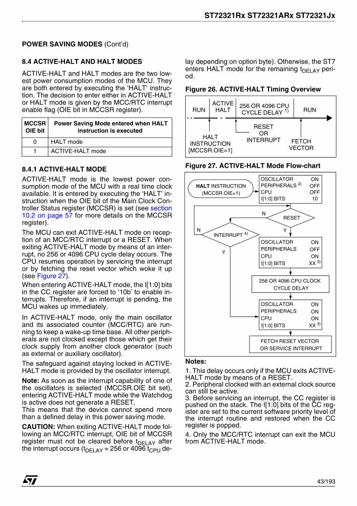
ST72321Rx ST72321ARx ST72321Jx
POWER SAVING MODES (Cont’d)
8.4 ACTIVE-HALT AND HALT MODES
ACTIVE-HALT and HALT modes are the two low-est power consumption modes of the MCU. Theyare both entered by executing the ‘HALT’ instruc-tion. The decision to enter either in ACTIVE-HALTor HALT mode is given by the MCC/RTC interruptenable flag (OIE bit in MCCSR register).
8.4.1 ACTIVE-HALT MODEACTIVE-HALT mode is the lowest power con-sumption mode of the MCU with a real time clockavailable. It is entered by executing the ‘HALT’ in-struction when the OIE bit of the Main Clock Con-troller Status register (MCCSR) is set (see section10.2 on page 57 for more details on the MCCSRregister).
The MCU can exit ACTIVE-HALT mode on recep-tion of an MCC/RTC interrupt or a RESET. Whenexiting ACTIVE-HALT mode by means of an inter-rupt, no 256 or 4096 CPU cycle delay occurs. TheCPU resumes operation by servicing the interruptor by fetching the reset vector which woke it up(see Figure 27).When entering ACTIVE-HALT mode, the I[1:0] bitsin the CC register are forced to ‘10b’ to enable in-terrupts. Therefore, if an interrupt is pending, theMCU wakes up immediately.
In ACTIVE-HALT mode, only the main oscillatorand its associated counter (MCC/RTC) are run-ning to keep a wake-up time base. All other periph-erals are not clocked except those which get theirclock supply from another clock generator (suchas external or auxiliary oscillator).
The safeguard against staying locked in ACTIVE-HALT mode is provided by the oscillator interrupt.
Note: As soon as the interrupt capability of one ofthe oscillators is selected (MCCSR.OIE bit set),entering ACTIVE-HALT mode while the Watchdogis active does not generate a RESET.This means that the device cannot spend morethan a defined delay in this power saving mode.
CAUTION: When exiting ACTIVE-HALT mode fol-lowing an MCC/RTC interrupt, OIE bit of MCCSRregister must not be cleared before tDELAY afterthe interrupt occurs (tDELAY = 256 or 4096 tCPU de-
lay depending on option byte). Otherwise, the ST7enters HALT mode for the remaining tDELAY peri-od.
Figure 26. ACTIVE-HALT Timing Overview
Figure 27. ACTIVE-HALT Mode Flow-chart
Notes:1. This delay occurs only if the MCU exits ACTIVE-HALT mode by means of a RESET.2. Peripheral clocked with an external clock sourcecan still be active.3. Before servicing an interrupt, the CC register ispushed on the stack. The I[1:0] bits of the CC reg-ister are set to the current software priority level ofthe interrupt routine and restored when the CCregister is popped.4. Only the MCC/RTC interrupt can exit the MCUfrom ACTIVE-HALT mode.
MCCSROIE bit
Power Saving Mode entered when HALT instruction is executed
0 HALT mode
1 ACTIVE-HALT mode
HALTRUN RUN256 OR 4096 CPUCYCLE DELAY 1)
RESETOR
INTERRUPTHALTINSTRUCTION FETCH
VECTOR
ACTIVE
[MCCSR.OIE=1]
HALT INSTRUCTION
RESET
Y
N
N
Y
CPU
OSCILLATOR PERIPHERALS 2)
I[1:0] BITS
ONOFF
10OFF
FETCH RESET VECTOROR SERVICE INTERRUPT
CPU
OSCILLATOR PERIPHERALS
I[1:0] BITS
ONOFF
XX 3)ON
CPU
OSCILLATOR PERIPHERALS
I[1:0] BITS
ONON
XX 3)ON
256 OR 4096 CPU CLOCKCYCLE DELAY
(MCCSR.OIE=1)
INTERRUPT 4)
43/193

ST72321Rx ST72321ARx ST72321Jx
POWER SAVING MODES (Cont’d)
8.4.2 HALT MODEThe HALT mode is the lowest power consumptionmode of the MCU. It is entered by executing the‘HALT’ instruction when the OIE bit of the MainClock Controller Status register (MCCSR) iscleared (see section 10.2 on page 57 for more de-tails on the MCCSR register).
The MCU can exit HALT mode on reception of ei-ther a specific interrupt (see Table 8, “InterruptMapping,” on page 37) or a RESET. When exitingHALT mode by means of a RESET or an interrupt,the oscillator is immediately turned on and the 256or 4096 CPU cycle delay is used to stabilize theoscillator. After the start up delay, the CPUresumes operation by servicing the interrupt or byfetching the reset vector which woke it up (see Fig-ure 29).When entering HALT mode, the I[1:0] bits in theCC register are forced to ‘10b’to enable interrupts.Therefore, if an interrupt is pending, the MCUwakes up immediately.
In HALT mode, the main oscillator is turned offcausing all internal processing to be stopped, in-cluding the operation of the on-chip peripherals.All peripherals are not clocked except the oneswhich get their clock supply from another clockgenerator (such as an external or auxiliary oscilla-tor).
The compatibility of Watchdog operation withHALT mode is configured by the “WDGHALT” op-tion bit of the option byte. The HALT instructionwhen executed while the Watchdog system is en-abled, can generate a Watchdog RESET (see sec-tion 14.1 on page 175 for more details).
Figure 28. HALT Timing Overview
Figure 29. HALT Mode Flow-chart
Notes:1. WDGHALT is an option bit. See option byte sec-tion for more details.2. Peripheral clocked with an external clock sourcecan still be active.3. Only some specific interrupts can exit the MCUfrom HALT mode (such as external interrupt). Re-fer to Table 8, “Interrupt Mapping,” on page 37 formore details.4. Before servicing an interrupt, the CC register ispushed on the stack. The I[1:0] bits of the CC reg-ister are set to the current software priority level ofthe interrupt routine and recovered when the CCregister is popped.
HALTRUN RUN256 OR 4096 CPU
CYCLE DELAY
RESETOR
INTERRUPTHALTINSTRUCTION FETCH
VECTOR[MCCSR.OIE=0]
HALT INSTRUCTION
RESET
INTERRUPT 3)
Y
N
N
Y
CPU
OSCILLATOR PERIPHERALS 2)
I[1:0] BITS
OFFOFF
10OFF
FETCH RESET VECTOROR SERVICE INTERRUPT
CPU
OSCILLATOR PERIPHERALS
I[1:0] BITS
ONOFF
XX 4)ON
CPU
OSCILLATOR PERIPHERALS
I[1:0] BITS
ONON
XX 4)ON
256 OR 4096 CPU CLOCKDELAY
WATCHDOGENABLE
DISABLEWDGHALT 1) 0
WATCHDOGRESET
1
(MCCSR.OIE=0)
CYCLE
44/193

ST72321Rx ST72321ARx ST72321Jx
POWER SAVING MODES (Cont’d)
8.4.2.1 Halt Mode Recommendations– Make sure that an external event is available to
wake up the microcontroller from Halt mode.
– When using an external interrupt to wake up the microcontroller, reinitialize the corresponding I/O as “Input Pull-up with Interrupt” before executing the HALT instruction. The main reason for this is that the I/O may be wrongly configured due to ex-ternal interference or by an unforeseen logical condition.
– For the same reason, reinitialize the level sensi-tiveness of each external interrupt as a precau-tionary measure.
– The opcode for the HALT instruction is 0x8E. To avoid an unexpected HALT instruction due to a program counter failure, it is advised to clear all occurrences of the data value 0x8E from memo-
ry. For example, avoid defining a constant in ROM with the value 0x8E.
– As the HALT instruction clears the interrupt mask in the CC register to allow interrupts, the user may choose to clear all pending interrupt bits be-fore executing the HALT instruction. This avoids entering other peripheral interrupt routines after executing the external interrupt routine corre-sponding to the wake-up event (reset or external interrupt).
Related DocumentationAN 980: ST7 Keypad Decoding Techniques, Im-plementing Wake-Up on Keystroke
AN1014: How to Minimize the ST7 Power Con-sumption
AN1605: Using an active RC to wakeup theST7LITE0 from power saving mode
45/193

ST72321Rx ST72321ARx ST72321Jx
9 I/O PORTS
9.1 INTRODUCTION
The I/O ports offer different functional modes:– transfer of data through digital inputs and outputs
and for specific pins:– external interrupt generation– alternate signal input/output for the on-chip pe-
ripherals.
An I/O port contains up to 8 pins. Each pin can beprogrammed independently as digital input (with orwithout interrupt generation) or digital output.
9.2 FUNCTIONAL DESCRIPTION
Each port has two main registers:
– Data Register (DR)
– Data Direction Register (DDR)
and one optional register:
– Option Register (OR)
Each I/O pin may be programmed using the corre-sponding register bits in the DDR and OR regis-ters: Bit X corresponding to pin X of the port. Thesame correspondence is used for the DR register.
The following description takes into account theOR register, (for specific ports which do not pro-vide this register refer to the I/O Port Implementa-tion section). The generic I/O block diagram isshown in Figure 1
9.2.1 Input ModesThe input configuration is selected by clearing thecorresponding DDR register bit.
In this case, reading the DR register returns thedigital value applied to the external I/O pin.
Different input modes can be selected by softwarethrough the OR register.Notes:1. Writing the DR register modifies the latch valuebut does not affect the pin status.2. When switching from input to output mode, theDR register has to be written first to drive the cor-rect level on the pin as soon as the port is config-ured as an output.3. Do not use read/modify/write instructions (BSETor BRES) to modify the DR register as this mightcorrupt the DR content for I/Os configured as input.External interrupt functionWhen an I/O is configured as Input with Interrupt,an event on this I/O can generate an external inter-rupt request to the CPU.
Each pin can independently generate an interruptrequest. The interrupt sensitivity is independentlyprogrammable using the sensitivity bits in theEICR register.
Each external interrupt vector is linked to a dedi-cated group of I/O port pins (see pinout descriptionand interrupt section). If several input pins are se-lected simultaneously as interrupt sources, theseare first detected according to the sensitivity bits inthe EICR register and then logically ORed.
The external interrupts are hardware interrupts,which means that the request latch (not accessibledirectly by the application) is automatically clearedwhen the corresponding interrupt vector isfetched. To clear an unwanted pending interruptby software, the sensitivity bits in the EICR registermust be modified.
9.2.2 Output ModesThe output configuration is selected by setting thecorresponding DDR register bit. In this case, writ-ing the DR register applies this digital value to theI/O pin through the latch. Then reading the DR reg-ister returns the previously stored value.
Two different output modes can be selected bysoftware through the OR register: Output push-pulland open-drain.
DR register value and output pin status:
9.2.3 Alternate FunctionsWhen an on-chip peripheral is configured to use apin, the alternate function is automatically select-ed. This alternate function takes priority over thestandard I/O programming.
When the signal is coming from an on-chip periph-eral, the I/O pin is automatically configured in out-put mode (push-pull or open drain according to theperipheral).
When the signal is going to an on-chip peripheral,the I/O pin must be configured in input mode. Inthis case, the pin state is also digitally readable byaddressing the DR register.
Note: Input pull-up configuration can cause unex-pected value at the input of the alternate peripheralinput. When an on-chip peripheral use a pin as in-put and output, this pin has to be configured in in-put floating mode.
DR Push-pull Open-drain0 VSS Vss1 VDD Floating
46/193

ST72321Rx ST72321ARx ST72321Jx
I/O PORTS (Cont’d)
Figure 30. I/O Port General Block Diagram
Table 10. I/O Port Mode Options
Legend: NI - not implementedOff - implemented not activatedOn - implemented and activated
Note: The diode to VDD is not implemented in thetrue open drain pads. A local protection betweenthe pad and VSS is implemented to protect the de-vice against positive stress.
Configuration Mode Pull-Up P-BufferDiodes
to VDD to VSS
InputFloating with/without Interrupt Off
OffOn
OnPull-up with/without Interrupt On
OutputPush-pull
OffOn
Open Drain (logic level) OffTrue Open Drain NI NI NI (see note)
DR
DDR
ORDA
TA
BU
S
PAD
VDD
ALTERNATEENABLE
ALTERNATEOUTPUT
1
0
OR SEL
DDR SEL
DR SEL
PULL-UPCONDITION
P-BUFFER(see table below)
N-BUFFER
PULL-UP(see table below)
1
0
ANALOGINPUT
If implemented
ALTERNATEINPUT
VDD
DIODES(see table below)
EXTERNAL
SOURCE (eix)INTERRUPT
CMOS SCHMITTTRIGGER
REGISTERACCESS
47/193

ST72321Rx ST72321ARx ST72321Jx
I/O PORTS (Cont’d)
Table 11. I/O Port Configurations
Notes:1. When the I/O port is in input configuration and the associated alternate function is enabled as an output,
reading the DR register will read the alternate function output status.2. When the I/O port is in output configuration and the associated alternate function is enabled as an input,
the alternate function reads the pin status given by the DR register content.
Hardware Configuration
INP
UT
1)O
PE
N-D
RA
INO
UT
PU
T2)
PU
SH
-PU
LLO
UT
PU
T2)
CONDITION
PAD
VDD
RPU
EXTERNAL INTERRUPT
DATA BUS
PULL-UP
INTERRUPT
DR REGISTER ACCESS
W
R
SOURCE (eix)
DRREGISTER
CONDITION
ALTERNATE INPUT
NOT IMPLEMENTED INTRUE OPEN DRAINI/O PORTS
ANALOG INPUT
PAD
RPU
DATA BUSDR
DR REGISTER ACCESS
R/W
VDD
ALTERNATEALTERNATEENABLE OUTPUT
REGISTER
NOT IMPLEMENTED INTRUE OPEN DRAINI/O PORTS
PAD
RPU
DATA BUSDR
DR REGISTER ACCESS
R/W
VDD
ALTERNATEALTERNATEENABLE OUTPUT
REGISTER
NOT IMPLEMENTED INTRUE OPEN DRAINI/O PORTS
48/193
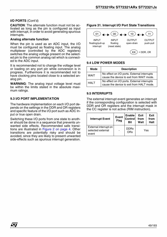
ST72321Rx ST72321ARx ST72321Jx
I/O PORTS (Cont’d)
CAUTION: The alternate function must not be ac-tivated as long as the pin is configured as inputwith interrupt, in order to avoid generating spuriousinterrupts.Analog alternate function When the pin is used as an ADC input, the I/Omust be configured as floating input. The analogmultiplexer (controlled by the ADC registers)switches the analog voltage present on the select-ed pin to the common analog rail which is connect-ed to the ADC input.
It is recommended not to change the voltage levelor loading on any port pin while conversion is inprogress. Furthermore it is recommended not tohave clocking pins located close to a selected an-alog pin.
WARNING: The analog input voltage level mustbe within the limits stated in the absolute maxi-mum ratings.
9.3 I/O PORT IMPLEMENTATION
The hardware implementation on each I/O port de-pends on the settings in the DDR and OR registersand specific feature of the I/O port such as ADC In-put or true open drain.
Switching these I/O ports from one state to anoth-er should be done in a sequence that prevents un-wanted side effects. Recommended safe transi-tions are illustrated in Figure 2 on page 4. Othertransitions are potentially risky and should beavoided, since they are likely to present unwantedside-effects such as spurious interrupt generation.
Figure 31. Interrupt I/O Port State Transitions
9.4 LOW POWER MODES
9.5 INTERRUPTS
The external interrupt event generates an interruptif the corresponding configuration is selected withDDR and OR registers and the interrupt mask inthe CC register is not active (RIM instruction).
Mode Description
WAITNo effect on I/O ports. External interrupts cause the device to exit from WAIT mode.
HALTNo effect on I/O ports. External interrupts cause the device to exit from HALT mode.
Interrupt EventEventFlag
Enable Control
Bit
Exit fromWait
Exit from Halt
External interrupt on selected external event
-DDRxORx
Yes
01
floating/pull-upinterrupt
INPUT
00
floating(reset state)
INPUT
10
open-drainOUTPUT
11
push-pullOUTPUT
XX = DDR, OR
49/193

ST72321Rx ST72321ARx ST72321Jx
I/O PORTS (Cont’d)
9.5.1 I/O Port ImplementationThe I/O port register configurations are summa-rised as follows.
Standard Ports
PA5:4, PC7:0, PD7:0, PE7:3,PE1:0, PF7:3,
Interrupt PortsPA2:0, PB6:5, PB4, PB2:0, PF1:0 (with pull-up)
PA3, PB7, PB3, PF2 (without pull-up)
True Open Drain PortsPA7:6
Pull-Up Input Port PE2
Table 12. Port Configuration
MODE DDR ORfloating input 0 0pull-up input 0 1open drain output 1 0push-pull output 1 1
MODE DDR ORfloating input 0 0pull-up interrupt input 0 1open drain output 1 0push-pull output 1 1
MODE DDR ORfloating input 0 0floating interrupt input 0 1open drain output 1 0push-pull output 1 1
MODE DDRfloating input 0open drain (high sink ports) 1
MODEpull-up input
Port Pin nameInput Output
OR = 0 OR = 1 OR = 0 OR = 1
Port A
PA7:6 floating true open-drain
PA5:4 floating pull-up open drain push-pull
PA3 floating floating interrupt open drain push-pull
PA2:0 floating pull-up interrupt open drain push-pull
Port BPB7, PB3 floating floating interrupt open drain push-pull
PB6:5, PB4, PB2:0 floating pull-up interrupt open drain push-pull
Port C PC7:0 floating pull-up open drain push-pull
Port D PD7:0 floating pull-up open drain push-pull
Port E
PE7:3, PE1:0 floating pull-up open drain push-pull
PE2 (Flash de-vices) pull-up input only
PE2 (ROM de-vices) floating floating open drain push-pull
Port F
PF7:3 floating pull-up open drain push-pull
PF2 floating floating interrupt open drain push-pull
PF1:0 floating pull-up interrupt open drain push-pull
50/193

ST72321Rx ST72321ARx ST72321Jx
I/O PORTS (Cont’d)
Table 13. I/O Port Register Map and Reset Values
Related DocumentationAN 970: SPI Communication between ST7 andEEPROM
AN1045: S/W implementation of I2C bus master
AN1048: Software LCD driver
Address(Hex.)
RegisterLabel
7 6 5 4 3 2 1 0
Reset Valueof all I/O port registers
0 0 0 0 0 0 0 0
0000h PADRMSB LSB0001h PADDR
0002h PAOR0003h PBDR
MSB LSB0004h PBDDR0005h PBOR0006h PCDR
MSB LSB0007h PCDDR0008h PCOR0009h PDDR
MSB LSB000Ah PDDDR000Bh PDOR000Ch PEDR
MSB LSB000Dh PEDDR000Eh PEOR000Fh PFDR
MSB LSB0010h PFDDR0011h PFOR
51/193

ST72321Rx ST72321ARx ST72321Jx
10 ON-CHIP PERIPHERALS
10.1 WATCHDOG TIMER (WDG)
10.1.1 IntroductionThe Watchdog timer is used to detect the occur-rence of a software fault, usually generated by ex-ternal interference or by unforeseen logical condi-tions, which causes the application program toabandon its normal sequence. The Watchdog cir-cuit generates an MCU reset on expiry of a pro-grammed time period, unless the program refresh-es the counter’s contents before the T6 bit be-comes cleared.
10.1.2 Main Features■ Programmable free-running downcounter■ Programmable reset ■ Reset (if watchdog activated) when the T6 bit
reaches zero■ Optional reset on HALT instruction
(configurable by option byte)■ Hardware Watchdog selectable by option byte
10.1.3 Functional DescriptionThe counter value stored in the Watchdog Controlregister (WDGCR bits T[6:0]), is decrementedevery 16384 fOSC2 cycles (approx.), and thelength of the timeout period can be programmedby the user in 64 increments.
If the watchdog is activated (the WDGA bit is set)and when the 7-bit timer (bits T[6:0]) rolls overfrom 40h to 3Fh (T6 becomes cleared), it initiatesa reset cycle pulling the reset pin low for typically30µs.
The application program must write in theWDGCR register at regular intervals during normaloperation to prevent an MCU reset. This down-counter is free-running: it counts down even if thewatchdog is disabled. The value to be stored in theWDGCR register must be between FFh and C0h:
– The WDGA bit is set (watchdog enabled)
– The T6 bit is set to prevent generating an imme-diate reset
– The T[5:0] bits contain the number of increments which represents the time delay before the watchdog produces a reset (see Figure 2. Ap-proximate Timeout Duration). The timing varies between a minimum and a maximum value due to the unknown status of the prescaler when writ-ing to the WDGCR register (see Figure 3).
Following a reset, the watchdog is disabled. Onceactivated it cannot be disabled, except by a reset.
The T6 bit can be used to generate a software re-set (the WDGA bit is set and the T6 bit is cleared).
If the watchdog is activated, the HALT instructionwill generate a Reset.
Figure 32. Watchdog Block Diagram
RESET
WDGA
6-BIT DOWNCOUNTER (CNT)
fOSC2
T6 T0
WDG PRESCALER
WATCHDOG CONTROL REGISTER (WDGCR)
DIV 4
T1T2T3T4T5
12-BIT MCC
RTC COUNTER
MSB LSB
DIV 64
05611
MCC/RTC
TB[1:0] bits(MCCSR Register)
52/193

ST72321Rx ST72321ARx ST72321Jx
WATCHDOG TIMER (Cont’d)
10.1.4 How to Program the Watchdog TimeoutFigure 2 shows the linear relationship between the6-bit value to be loaded in the Watchdog Counter(CNT) and the resulting timeout duration in milli-seconds. This can be used for a quick calculationwithout taking the timing variations into account. If
more precision is needed, use the formulae in Fig-ure 3.
Caution: When writing to the WDGCR register, al-ways write 1 in the T6 bit to avoid generating animmediate reset.
Figure 33. Approximate Timeout Duration
CN
T V
alu
e (h
ex.)
Watchdog timeout (ms) @ 8 MHz. fOSC2
3F
00
38
1281.5 65
30
28
20
18
10
08
503418 82 98 114
53/193

ST72321Rx ST72321ARx ST72321Jx
WATCHDOG TIMER (Cont’d)
Figure 34. Exact Timeout Duration (tmin and tmax)WHERE:tmin0 = (LSB + 128) x 64 x tOSC2tmax0 = 16384 x tOSC2tOSC2 = 125ns if fOSC2=8 MHz
CNT = Value of T[5:0] bits in the WDGCR register (6 bits)MSB and LSB are values from the table below depending on the timebase selected by the TB[1:0] bitsin the MCCSR register
To calculate the minimum Watchdog Timeout (tmin):
IF THEN
ELSE
To calculate the maximum Watchdog Timeout (tmax):
IF THEN
ELSE
Note: In the above formulae, division results must be rounded down to the next integer value.
Example:With 2ms timeout selected in MCCSR register
TB1 Bit
(MCCSR Reg.)
TB0 Bit
(MCCSR Reg.)Selected MCCSR
TimebaseMSB LSB
0 0 2ms 4 590 1 4ms 8 531 0 10ms 20 351 1 25ms 49 54
Value of T[5:0] Bits in WDGCR Register (Hex.)
Min. Watchdog Timeout (ms)
tmin
Max. Watchdog Timeout (ms)
tmax00 1.496 2.0483F 128 128.552
CNT MSB4
-------------< tmin tmin0 16384 CNT tosc2××+=
tmin tmin0 16384 CNT 4CNTMSB-----------------–⎝ ⎠
⎛ ⎞× 192 LSB+( ) 64 4CNTMSB-----------------××+ tosc2×+=
CNTMSB
4-------------≤ tmax tmax0 16384 CNT tosc2××+=
tmax tmax0 16384 CNT 4CNTMSB-----------------–⎝ ⎠
⎛ ⎞× 192 LSB+( ) 64 4CNTMSB-----------------××+ tosc2×+=
54/193

ST72321Rx ST72321ARx ST72321Jx
WATCHDOG TIMER (Cont’d)
10.1.5 Low Power Modes
10.1.6 Hardware Watchdog OptionIf Hardware Watchdog is selected by option byte,the watchdog is always active and the WDGA bit inthe WDGCR is not used. Refer to the Option Bytedescription.
10.1.7 Using Halt Mode with the WDG(WDGHALT option)The following recommendation applies if Haltmode is used when the watchdog is enabled.
– Before executing the HALT instruction, refresh the WDG counter, to avoid an unexpected WDG reset immediately after waking up the microcon-troller.
10.1.8 InterruptsNone.
10.1.9 Register DescriptionCONTROL REGISTER (WDGCR)Read/Write
Reset Value: 0111 1111 (7Fh)
Bit 7 = WDGA Activation bit.This bit is set by software and only cleared byhardware after a reset. When WDGA = 1, thewatchdog can generate a reset.0: Watchdog disabled1: Watchdog enabled
Note: This bit is not used if the hardware watch-dog option is enabled by option byte.
Bit 6:0 = T[6:0] 7-bit counter (MSB to LSB).These bits contain the value of the watchdogcounter. It is decremented every 16384 fOSC2 cy-cles (approx.). A reset is produced when it rollsover from 40h to 3Fh (T6 becomes cleared).
Mode Description SLOW No effect on Watchdog. WAIT No effect on Watchdog.
HALT
OIE bit in MCCSR register
WDGHALT bit in Option
Byte
0 0
No Watchdog reset is generated. The MCU enters Halt mode. The Watch-dog counter is decremented once and then stops counting and is no longer able to generate a watchdog reset until the MCU receives an external inter-rupt or a reset.
If an external interrupt is received, the Watchdog restarts counting after 256 or 4096 CPU clocks. If a reset is generated, the Watchdog is disabled (reset state) unless Hardware Watchdog is selected by option byte. For applica-tion recommendations see Section 0.1.7 below.
0 1 A reset is generated.
1 x
No reset is generated. The MCU enters Active Halt mode. The Watchdog counter is not decremented. It stop counting. When the MCU receives an oscillator interrupt or external interrupt, the Watchdog restarts counting im-mediately. When the MCU receives a reset the Watchdog restarts counting after 256 or 4096 CPU clocks.
7 0
WDGA T6 T5 T4 T3 T2 T1 T0
55/193

ST72321Rx ST72321ARx ST72321Jx
Table 14. Watchdog Timer Register Map and Reset Values
Address(Hex.)
RegisterLabel
7 6 5 4 3 2 1 0
002AhWDGCRReset Value
WDGA0
T61
T51
T41
T31
T21
T11
T01
56/193

ST72321Rx ST72321ARx ST72321Jx
10.2 MAIN CLOCK CONTROLLER WITH REAL TIME CLOCK AND BEEPER (MCC/RTC)
The Main Clock Controller consists of three differ-ent functions:■ a programmable CPU clock prescaler■ a clock-out signal to supply external devices■ a real time clock timer with interrupt capability
Each function can be used independently and si-multaneously.10.2.1 Programmable CPU Clock PrescalerThe programmable CPU clock prescaler suppliesthe clock for the ST7 CPU and its internal periph-erals. It manages SLOW power saving mode (SeeSection 8.2 SLOW MODE for more details).
The prescaler selects the fCPU main clock frequen-cy and is controlled by three bits in the MCCSRregister: CP[1:0] and SMS.10.2.2 Clock-out CapabilityThe clock-out capability is an alternate function ofan I/O port pin that outputs a fCPU clock to drive
external devices. It is controlled by the MCO bit inthe MCCSR register.CAUTION: When selected, the clock out pin sus-pends the clock during ACTIVE-HALT mode.10.2.3 Real Time Clock Timer (RTC)The counter of the real time clock timer allows aninterrupt to be generated based on an accuratereal time clock. Four different time bases depend-ing directly on fOSC2 are available. The wholefunctionality is controlled by four bits of the MCC-SR register: TB[1:0], OIE and OIF.
When the RTC interrupt is enabled (OIE bit set),the ST7 enters ACTIVE-HALT mode when theHALT instruction is executed. See Section 8.4 AC-TIVE-HALT AND HALT MODES for more details.10.2.4 BeeperThe beep function is controlled by the MCCBCRregister. It can output three selectable frequencieson the BEEP pin (I/O port alternate function).
Figure 35. Main Clock Controller (MCC/RTC) Block Diagram
DIV 2, 4, 8, 16
MCC/RTC INTERRUPT
SMSCP1 CP0 TB1 TB0 OIE OIF
CPU CLOCK
MCCSR
12-BIT MCC RTCCOUNTER
TO CPU ANDPERIPHERALS
fOSC2
fCPU
MCO
MCO
BC1 BC0
MCCBCR
BEEP
SELECTIONBEEP SIGNAL
1
0
TOWATCHDOG
TIMER
DIV 64
57/193

ST72321Rx ST72321ARx ST72321Jx
MAIN CLOCK CONTROLLER WITH REAL TIME CLOCK (Cont’d)
10.2.5 Low Power Modes
10.2.6 InterruptsThe MCC/RTC interrupt event generates an inter-rupt if the OIE bit of the MCCSR register is set andthe interrupt mask in the CC register is not active(RIM instruction).
Note:The MCC/RTC interrupt wakes up the MCU fromACTIVE-HALT mode, not from HALT mode.
10.2.7 Register DescriptionMCC CONTROL/STATUS REGISTER (MCCSR)Read/Write
Reset Value: 0000 0000 (00h)
Bit 7 = MCO Main clock out selectionThis bit enables the MCO alternate function on thePF0 I/O port. It is set and cleared by software.0: MCO alternate function disabled (I/O pin free for
general-purpose I/O)1: MCO alternate function enabled (fCPU on I/O
port)
Note: To reduce power consumption, the MCOfunction is not active in ACTIVE-HALT mode.
Bit 6:5 = CP[1:0] CPU clock prescalerThese bits select the CPU clock prescaler which isapplied in the different slow modes. Their action isconditioned by the setting of the SMS bit. Thesetwo bits are set and cleared by software
Bit 4 = SMS Slow mode selectThis bit is set and cleared by software.0: Normal mode. fCPU = fOSC21: Slow mode. fCPU is given by CP1, CP0See Section 8.2 SLOW MODE and Section 10.2MAIN CLOCK CONTROLLER WITH REAL TIMECLOCK AND BEEPER (MCC/RTC) for more de-tails.
Bit 3:2 = TB[1:0] Time base control
These bits select the programmable divider timebase. They are set and cleared by software.
A modification of the time base is taken into ac-count at the end of the current period (previouslyset) to avoid an unwanted time shift. This allows touse this time base as a real time clock.
Bit 1 = OIE Oscillator interrupt enableThis bit set and cleared by software.0: Oscillator interrupt disabled1: Oscillator interrupt enabledThis interrupt can be used to exit from ACTIVE-HALT mode.When this bit is set, calling the ST7 software HALTinstruction enters the ACTIVE-HALT power savingmode.
Mode Description
WAITNo effect on MCC/RTC peripheral.MCC/RTC interrupt cause the device to exit from WAIT mode.
ACTIVE-HALT
No effect on MCC/RTC counter (OIE bit is set), the registers are frozen.MCC/RTC interrupt cause the device to exit from ACTIVE-HALT mode.
HALT
MCC/RTC counter and registers are frozen.MCC/RTC operation resumes when the MCU is woken up by an interrupt with “exit from HALT” capability.
Interrupt EventEventFlag
Enable Control
Bit
Exit fromWait
Exit from Halt
Time base overflow event
OIF OIE Yes No 1)
7 0
MCO CP1 CP0 SMS TB1 TB0 OIE OIF
fCPU in SLOW mode CP1 CP0
fOSC2 / 2 0 0
fOSC2 / 4 0 1
fOSC2 / 8 1 0
fOSC2 / 16 1 1
Counter Prescaler
Time BaseTB1 TB0
fOSC2 =4MHz fOSC2=8MHz
16000 4ms 2ms 0 0
32000 8ms 4ms 0 1
80000 20ms 10ms 1 0
200000 50ms 25ms 1 1
58/193

ST72321Rx ST72321ARx ST72321Jx
MAIN CLOCK CONTROLLER WITH REAL TIME CLOCK (Cont’d)
Bit 0 = OIF Oscillator interrupt flagThis bit is set by hardware and cleared by softwarereading the MCCSR register. It indicates when setthat the main oscillator has reached the selectedelapsed time (TB1:0). 0: Timeout not reached1: Timeout reached
CAUTION: The BRES and BSET instructionsmust not be used on the MCCSR register to avoidunintentionally clearing the OIF bit.
MCC BEEP CONTROL REGISTER (MCCBCR)Read/Write
Reset Value: 0000 0000 (00h)
Bit 7:2 = Reserved, must be kept cleared.
Bit 1:0 = BC[1:0] Beep controlThese 2 bits select the PF1 pin beep capability.
The beep output signal is available in ACTIVE-HALT mode but has to be disabled to reduce theconsumption.
Table 15. Main Clock Controller Register Map and Reset Values
7 0
0 0 0 0 0 0 BC1 BC0
BC1 BC0 Beep mode with fOSC2=8MHz
0 0 Off
0 1 ~2-KHz Output
Beep signal~50% duty cycle
1 0 ~1-KHz
1 1 ~500-Hz
Address(Hex.)
RegisterLabel
7 6 5 4 3 2 1 0
002BhSICSRReset Value
AVDS0
AVDIE0
AVDF0
LVDRFx 0 0 0
WDGRFx
002ChMCCSRReset Value
MCO0
CP10
CP00
SMS0
TB10
TB00
OIE0
OIF0
002DhMCCBCRReset Value 0 0 0 0 0 0
BC10
BC00
59/193

ST72321Rx ST72321ARx ST72321Jx
10.3 PWM AUTO-RELOAD TIMER (ART)
10.3.1 IntroductionThe Pulse Width Modulated Auto-Reload Timeron-chip peripheral consists of an 8-bit auto reloadcounter with compare/capture capabilities and of a7-bit prescaler clock source.
These resources allow five possible operatingmodes:
– Generation of up to 4 independent PWM signals
– Output compare and Time base interrupt
– Up to two input capture functions
– External event detector
– Up to two external interrupt sources
The three first modes can be used together with asingle counter frequency.
The timer can be used to wake up the MCU fromWAIT and HALT modes.
Figure 36. PWM Auto-Reload Timer Block Diagram
OVF INTERRUPT
EXCL CC2 CC1 CC0 TCE FCRL OIE OVF ARTCSR
fINPUT
PWMxPORT
FUNCTIONALTERNATE
OCRx
COMPARE
REGISTER
PROGRAMMABLE
PRESCALER
8-BIT COUNTER
(CAR REGISTER)
ARR
REGISTER
ICRx
REGISTER
LOAD
OPx
POLARITY
CONTROL
OExPWMCR
MUX
fCPU
DCRx
REGISTER
LOAD
fCOUNTERARTCLK
fEXT
ARTICx
ICFxICSx ICCSR
LOAD
ICx INTERRUPT
ICIEx
INPUT CAPTURE
CONTROL
60/193
ST72321Rx ST72321ARx ST72321Jx
ON-CHIP PERIPHERALS (Cont’d)
10.3.2 Functional Description
CounterThe free running 8-bit counter is fed by the outputof the prescaler, and is incremented on every ris-ing edge of the clock signal.
It is possible to read or write the contents of thecounter on the fly by reading or writing the CounterAccess register (ARTCAR).
When a counter overflow occurs, the counter isautomatically reloaded with the contents of theARTARR register (the prescaler is not affected).
Counter clock and prescalerThe counter clock frequency is given by:
fCOUNTER = fINPUT / 2CC[2:0]
The timer counter’s input clock (fINPUT) feeds the7-bit programmable prescaler, which selects oneof the 8 available taps of the prescaler, as definedby CC[2:0] bits in the Control/Status Register(ARTCSR). Thus the division factor of the prescal-er can be set to 2n (where n = 0, 1,..7).
This fINPUT frequency source is selected throughthe EXCL bit of the ARTCSR register and can beeither the fCPU or an external input frequency fEXT.
The clock input to the counter is enabled by theTCE (Timer Counter Enable) bit in the ARTCSRregister. When TCE is reset, the counter isstopped and the prescaler and counter contentsare frozen. When TCE is set, the counter runs atthe rate of the selected clock source.
Counter and Prescaler InitializationAfter RESET, the counter and the prescaler arecleared and fINPUT = fCPU.
The counter can be initialized by:
– Writing to the ARTARR register and then setting the FCRL (Force Counter Re-Load) and the TCE (Timer Counter Enable) bits in the ARTCSR reg-ister.
– Writing to the ARTCAR counter access register,
In both cases the 7-bit prescaler is also cleared,whereupon counting will start from a known value.
Direct access to the prescaler is not possible.
Output compare controlThe timer compare function is based on four differ-ent comparisons with the counter (one for eachPWMx output). Each comparison is made be-tween the counter value and an output compareregister (OCRx) value. This OCRx register can notbe accessed directly, it is loaded from the duty cy-cle register (PWMDCRx) at each overflow of thecounter.
This double buffering method avoids glitch gener-ation when changing the duty cycle on the fly.
Figure 37. Output compare control
COUNTER FDh FEh FFh FDh FEh FFh FDh FEh
ARTARR=FDh
fCOUNTER
OCRx
PWMDCRx FDh FEh
FDh FEh
FFh
PWMx
61/193

ST72321Rx ST72321ARx ST72321Jx
ON-CHIP PERIPHERALS (Cont’d)
Independent PWM signal generationThis mode allows up to four Pulse Width Modulat-ed signals to be generated on the PWMx outputpins with minimum core processing overhead.This function is stopped during HALT mode.
Each PWMx output signal can be selected inde-pendently using the corresponding OEx bit in thePWM Control register (PWMCR). When this bit isset, the corresponding I/O pin is configured as out-put push-pull alternate function.
The PWM signals all have the same frequencywhich is controlled by the counter period and theARTARR register value.
fPWM = fCOUNTER / (256 - ARTARR)
When a counter overflow occurs, the PWMx pinlevel is changed depending on the correspondingOPx (output polarity) bit in the PWMCR register.
When the counter reaches the value contained inone of the output compare register (OCRx) thecorresponding PWMx pin level is restored.
It should be noted that the reload values will alsoaffect the value and the resolution of the duty cycleof the PWM output signal. To obtain a signal on aPWMx pin, the contents of the OCRx register mustbe greater than the contents of the ARTARR reg-ister.
The maximum available resolution for the PWMxduty cycle is:
Resolution = 1 / (256 - ARTARR)
Note: To get the maximum resolution (1/256), theARTARR register must be 0. With this maximumresolution, 0% and 100% can be obtained bychanging the polarity.
Figure 38. PWM Auto-reload Timer Function
Figure 39. PWM Signal from 0% to 100% Duty Cycle
DUTY CYCLEREGISTER
AUTO-RELOADREGISTER
PW
Mx
OU
TP
UT
t
255
000
WITH OEx=1AND OPx=0
(ARTARR)
(PWMDCRx)
WITH OEx=1AND OPx=1
CO
UN
TE
R
COUNTER
PW
Mx
OU
TP
UT
t
WIT
H O
Ex=
1A
ND
OP
x=0
FDh FEh FFh FDh FEh FFh FDh FEh
OCRx=FCh
OCRx=FDh
OCRx=FEh
OCRx=FFh
ARTARR=FDh
fCOUNTER
62/193

ST72321Rx ST72321ARx ST72321Jx
ON-CHIP PERIPHERALS (Cont’d)
Output compare and Time base interruptOn overflow, the OVF flag of the ARTCSR registeris set and an overflow interrupt request is generat-ed if the overflow interrupt enable bit, OIE, in theARTCSR register, is set. The OVF flag must be re-set by the user software. This interrupt can beused as a time base in the application.
External clock and event detector modeUsing the fEXT external prescaler input clock, theauto-reload timer can be used as an external clockevent detector. In this mode, the ARTARR registeris used to select the nEVENT number of events tobe counted before setting the OVF flag.
nEVENT = 256 - ARTARR
Caution: The external clock function is not availa-ble in HALT mode. If HALT mode is used in the ap-plication, prior to executing the HALT instruction,the counter must be disabled by clearing the TCEbit in the ARTCSR register to avoid spurious coun-ter increments.
Figure 40. External Event Detector Example (3 counts)
COUNTER
t
FDh FEh FFh FDh
OVF
ARTCSR READ
INTERRUPT
ARTARR=FDh
fEXT=fCOUNTER
FEh FFh FDh
IF OIE=1INTERRUPT
IF OIE=1
ARTCSR READ
63/193
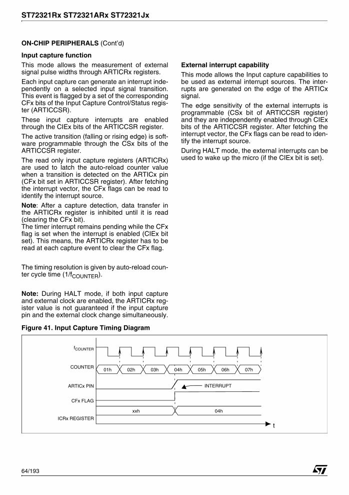
ST72321Rx ST72321ARx ST72321Jx
ON-CHIP PERIPHERALS (Cont’d)
Input capture functionThis mode allows the measurement of externalsignal pulse widths through ARTICRx registers.
Each input capture can generate an interrupt inde-pendently on a selected input signal transition.This event is flagged by a set of the correspondingCFx bits of the Input Capture Control/Status regis-ter (ARTICCSR).
These input capture interrupts are enabledthrough the CIEx bits of the ARTICCSR register.
The active transition (falling or rising edge) is soft-ware programmable through the CSx bits of theARTICCSR register.
The read only input capture registers (ARTICRx)are used to latch the auto-reload counter valuewhen a transition is detected on the ARTICx pin(CFx bit set in ARTICCSR register). After fetchingthe interrupt vector, the CFx flags can be read toidentify the interrupt source.
Note: After a capture detection, data transfer inthe ARTICRx register is inhibited until it is read(clearing the CFx bit).The timer interrupt remains pending while the CFxflag is set when the interrupt is enabled (CIEx bitset). This means, the ARTICRx register has to beread at each capture event to clear the CFx flag.
The timing resolution is given by auto-reload coun-ter cycle time (1/fCOUNTER).
Note: During HALT mode, if both input captureand external clock are enabled, the ARTICRx reg-ister value is not guaranteed if the input capturepin and the external clock change simultaneously.
External interrupt capabilityThis mode allows the Input capture capabilities tobe used as external interrupt sources. The inter-rupts are generated on the edge of the ARTICxsignal.
The edge sensitivity of the external interrupts isprogrammable (CSx bit of ARTICCSR register)and they are independently enabled through CIExbits of the ARTICCSR register. After fetching theinterrupt vector, the CFx flags can be read to iden-tify the interrupt source.
During HALT mode, the external interrupts can beused to wake up the micro (if the CIEx bit is set).
Figure 41. Input Capture Timing Diagram
04hCOUNTER
t
01h
fCOUNTER
xxh
02h 03h 05h 06h 07h
04h
ARTICx PIN
CFx FLAG
ICRx REGISTER
INTERRUPT
64/193

ST72321Rx ST72321ARx ST72321Jx
ON-CHIP PERIPHERALS (Cont’d)
10.3.3 Register Description
CONTROL / STATUS REGISTER (ARTCSR)Read/Write
Reset Value: 0000 0000 (00h)
Bit 7 = EXCL External ClockThis bit is set and cleared by software. It selects theinput clock for the 7-bit prescaler.0: CPU clock.1: External clock.
Bit 6:4 = CC[2:0] Counter Clock ControlThese bits are set and cleared by software. Theydetermine the prescaler division ratio from fINPUT.
Bit 3 = TCE Timer Counter EnableThis bit is set and cleared by software. It puts thetimer in the lowest power consumption mode.0: Counter stopped (prescaler and counter frozen).1: Counter running.
Bit 2 = FCRL Force Counter Re-LoadThis bit is write-only and any attempt to read it willyield a logical zero. When set, it causes the contentsof ARTARR register to be loaded into the counter,and the content of the prescaler register to becleared in order to initialize the timer before startingto count.
Bit 1 = OIE Overflow Interrupt EnableThis bit is set and cleared by software. It allows toenable/disable the interrupt which is generatedwhen the OVF bit is set.0: Overflow Interrupt disable.1: Overflow Interrupt enable.
Bit 0 = OVF Overflow FlagThis bit is set by hardware and cleared by softwarereading the ARTCSR register. It indicates the tran-sition of the counter from FFh to the ARTARR val-ue.
0: New transition not yet reached1: Transition reached
COUNTER ACCESS REGISTER (ARTCAR)Read/Write
Reset Value: 0000 0000 (00h)
Bit 7:0 = CA[7:0] Counter Access Data
These bits can be set and cleared either by hard-ware or by software. The ARTCAR register is usedto read or write the auto-reload counter “on the fly”(while it is counting).
AUTO-RELOAD REGISTER (ARTARR)Read/Write
Reset Value: 0000 0000 (00h)
Bit 7:0 = AR[7:0] Counter Auto-Reload Data
These bits are set and cleared by software. Theyare used to hold the auto-reload value which is au-tomatically loaded in the counter when an overflowoccurs. At the same time, the PWM output levelsare changed according to the corresponding OPxbit in the PWMCR register.
This register has two PWM management func-tions:
– Adjusting the PWM frequency– Setting the PWM duty cycle resolution
PWM Frequency vs Resolution:
7 0
EXCL CC2 CC1 CC0 TCE FCRL OIE OVF
fCOUNTER With fINPUT=8 MHz CC2 CC1 CC0
fINPUTfINPUT / 2fINPUT / 4fINPUT / 8
fINPUT / 16fINPUT / 32fINPUT / 64fINPUT / 128
8 MHz4 MHz2 MHz1 MHz
500 kHz250 kHz125 kHz62.5 kHz
00001111
00110011
01010101
7 0
CA7 CA6 CA5 CA4 CA3 CA2 CA1 CA0
7 0
AR7 AR6 AR5 AR4 AR3 AR2 AR1 AR0
ARTARR value
ResolutionfPWM
Min Max
0 8-bit ~0.244 kHz 31.25 kHz[ 0..127 ] > 7-bit ~0.244 kHz 62.5 kHz
[ 128..191 ] > 6-bit ~0.488 kHz 125 kHz[ 192..223 ] > 5-bit ~0.977 kHz 250 kHz[ 224..239 ] > 4-bit ~1.953 kHz 500 kHz
65/193

ST72321Rx ST72321ARx ST72321Jx
ON-CHIP PERIPHERALS (Cont’d)
PWM CONTROL REGISTER (PWMCR)Read/Write
Reset Value: 0000 0000 (00h)
Bit 7:4 = OE[3:0] PWM Output EnableThese bits are set and cleared by software. Theyenable or disable the PWM output channels inde-pendently acting on the corresponding I/O pin.0: PWM output disabled.1: PWM output enabled.
Bit 3:0 = OP[3:0] PWM Output PolarityThese bits are set and cleared by software. Theyindependently select the polarity of the four PWMoutput signals.
Note: When an OPx bit is modified, the PWMx out-put signal polarity is immediately reversed.
DUTY CYCLE REGISTERS (PWMDCRx)Read/Write
Reset Value: 0000 0000 (00h)
Bit 7:0 = DC[7:0] Duty Cycle Data
These bits are set and cleared by software.
A PWMDCRx register is associated with the OCRxregister of each PWM channel to determine thesecond edge location of the PWM signal (the firstedge location is common to all channels and givenby the ARTARR register). These PWMDCR regis-ters allow the duty cycle to be set independentlyfor each PWM channel.
7 0
OE3 OE2 OE1 OE0 OP3 OP2 OP1 OP0
PWMx output levelOPx
Counter <= OCRx Counter > OCRx
1 0 00 1 1
7 0
DC7 DC6 DC5 DC4 DC3 DC2 DC1 DC0
66/193

ST72321Rx ST72321ARx ST72321Jx
ON-CHIP PERIPHERALS (Cont’d)
INPUT CAPTURECONTROL / STATUS REGISTER (ARTICCSR)Read/Write
Reset Value: 0000 0000 (00h)
Bit 7:6 = Reserved, always read as 0.
Bit 5:4 = CS[2:1] Capture SensitivityThese bits are set and cleared by software. Theydetermine the trigger event polarity on the corre-sponding input capture channel.0: Falling edge triggers capture on channel x.1: Rising edge triggers capture on channel x.
Bit 3:2 = CIE[2:1] Capture Interrupt EnableThese bits are set and cleared by software. Theyenable or disable the Input capture channel inter-rupts independently.0: Input capture channel x interrupt disabled.1: Input capture channel x interrupt enabled.
Bit 1:0 = CF[2:1] Capture FlagThese bits are set by hardware and cleared bysoftware reading the corresponding ARTICRx reg-ister. Each CFx bit indicates that an input capture xhas occurred.0: No input capture on channel x.1: An input capture has occurred on channel x.
INPUT CAPTURE REGISTERS (ARTICRx)Read only
Reset Value: 0000 0000 (00h)
Bit 7:0 = IC[7:0] Input Capture Data
These read only bits are set and cleared by hard-ware. An ARTICRx register contains the 8-bitauto-reload counter value transferred by the inputcapture channel x event.
7 0
0 0 CS2 CS1 CIE2 CIE1 CF2 CF1
7 0
IC7 IC6 IC5 IC4 IC3 IC2 IC1 IC0
67/193
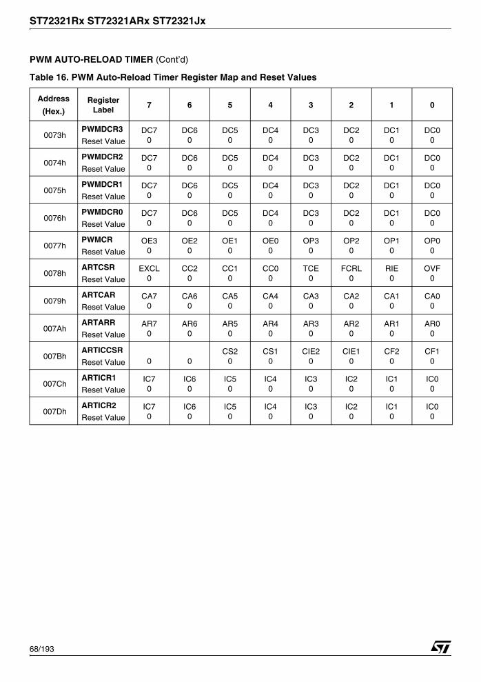
ST72321Rx ST72321ARx ST72321Jx
PWM AUTO-RELOAD TIMER (Cont’d)
Table 16. PWM Auto-Reload Timer Register Map and Reset Values
Address
(Hex.)Register
Label7 6 5 4 3 2 1 0
0073hPWMDCR3
Reset ValueDC7
0DC6
0DC5
0DC4
0DC3
0DC2
0DC1
0DC0
0
0074hPWMDCR2
Reset ValueDC7
0DC6
0DC5
0DC4
0DC3
0DC2
0DC1
0DC0
0
0075hPWMDCR1
Reset ValueDC7
0DC6
0DC5
0DC4
0DC3
0DC2
0DC1
0DC0
0
0076hPWMDCR0
Reset ValueDC7
0DC6
0DC5
0DC4
0DC3
0DC2
0DC1
0DC0
0
0077hPWMCR
Reset ValueOE3
0OE2
0OE1
0OE0
0OP3
0OP2
0OP1
0OP0
0
0078hARTCSR
Reset ValueEXCL
0CC2
0CC1
0CC0
0TCE
0FCRL
0RIE0
OVF0
0079hARTCAR
Reset ValueCA7
0CA6
0CA5
0CA4
0CA3
0CA2
0CA1
0CA0
0
007AhARTARR
Reset ValueAR7
0AR6
0AR5
0AR4
0AR3
0AR2
0AR1
0AR0
0
007BhARTICCSR
Reset Value 0 0CS2
0CS1
0CIE2
0CIE1
0CF2
0CF1
0
007ChARTICR1
Reset ValueIC70
IC60
IC50
IC40
IC30
IC20
IC10
IC00
007DhARTICR2
Reset ValueIC70
IC60
IC50
IC40
IC30
IC20
IC10
IC00
68/193
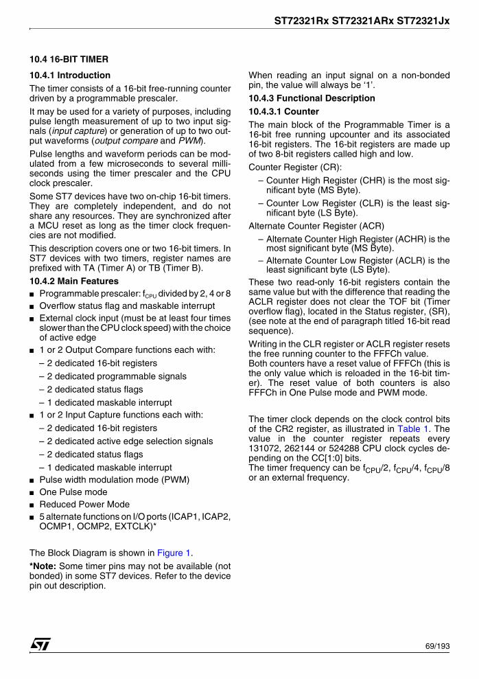
ST72321Rx ST72321ARx ST72321Jx
10.4 16-BIT TIMER
10.4.1 IntroductionThe timer consists of a 16-bit free-running counterdriven by a programmable prescaler.
It may be used for a variety of purposes, includingpulse length measurement of up to two input sig-nals (input capture) or generation of up to two out-put waveforms (output compare and PWM).
Pulse lengths and waveform periods can be mod-ulated from a few microseconds to several milli-seconds using the timer prescaler and the CPUclock prescaler.
Some ST7 devices have two on-chip 16-bit timers.They are completely independent, and do notshare any resources. They are synchronized aftera MCU reset as long as the timer clock frequen-cies are not modified.
This description covers one or two 16-bit timers. InST7 devices with two timers, register names areprefixed with TA (Timer A) or TB (Timer B).
10.4.2 Main Features■ Programmable prescaler: fCPU divided by 2, 4 or 8■ Overflow status flag and maskable interrupt■ External clock input (must be at least four times
slower than the CPU clock speed) with the choiceof active edge
■ 1 or 2 Output Compare functions each with:
– 2 dedicated 16-bit registers
– 2 dedicated programmable signals
– 2 dedicated status flags
– 1 dedicated maskable interrupt■ 1 or 2 Input Capture functions each with:
– 2 dedicated 16-bit registers
– 2 dedicated active edge selection signals
– 2 dedicated status flags
– 1 dedicated maskable interrupt■ Pulse width modulation mode (PWM)■ One Pulse mode ■ Reduced Power Mode■ 5 alternate functions on I/O ports (ICAP1, ICAP2,
OCMP1, OCMP2, EXTCLK)*
The Block Diagram is shown in Figure 1.
*Note: Some timer pins may not be available (notbonded) in some ST7 devices. Refer to the devicepin out description.
When reading an input signal on a non-bondedpin, the value will always be ‘1’.
10.4.3 Functional Description10.4.3.1 CounterThe main block of the Programmable Timer is a16-bit free running upcounter and its associated16-bit registers. The 16-bit registers are made upof two 8-bit registers called high and low.
Counter Register (CR):
– Counter High Register (CHR) is the most sig-nificant byte (MS Byte).
– Counter Low Register (CLR) is the least sig-nificant byte (LS Byte).
Alternate Counter Register (ACR)– Alternate Counter High Register (ACHR) is the
most significant byte (MS Byte).– Alternate Counter Low Register (ACLR) is the
least significant byte (LS Byte).These two read-only 16-bit registers contain thesame value but with the difference that reading theACLR register does not clear the TOF bit (Timeroverflow flag), located in the Status register, (SR),(see note at the end of paragraph titled 16-bit readsequence).
Writing in the CLR register or ACLR register resetsthe free running counter to the FFFCh value.Both counters have a reset value of FFFCh (this isthe only value which is reloaded in the 16-bit tim-er). The reset value of both counters is alsoFFFCh in One Pulse mode and PWM mode.
The timer clock depends on the clock control bitsof the CR2 register, as illustrated in Table 1. Thevalue in the counter register repeats every131072, 262144 or 524288 CPU clock cycles de-pending on the CC[1:0] bits.The timer frequency can be fCPU/2, fCPU/4, fCPU/8or an external frequency.
69/193

ST72321Rx ST72321ARx ST72321Jx
16-BIT TIMER (Cont’d)
Figure 42. Timer Block Diagram
MCU-PERIPHERAL INTERFACE
COUNTERALTERNATE
OUTPUTCOMPAREREGISTER
OUTPUT COMPARE EDGE DETECTOVERFLOW
DETECTCIRCUIT
1/21/4
1/8
8-bitbuffer
ST7 INTERNAL BUS
LATCH1 OCMP1
ICAP1
EXTCLK
fCPU
TIMER INTERRUPT
ICF2ICF1 TIMD 0 0OCF2OCF1 TOF
PWMOC1E EXEDGIEDG2CC0CC1OC2E OPMFOLV2ICIE OLVL1IEDG1OLVL2FOLV1OCIE TOIE
ICAP2
LATCH2 OCMP2
8 8
8 low
16
8 high
16 16
16 16
(Control Register 1) CR1 (Control Register 2) CR2
(Control/Status Register)
6
16
8 8 888 8
high
low
high
high
high
low
low
lowEXEDG
TIMER INTERNAL BUS
CIRCUIT1
EDGE DETECTCIRCUIT2
CIRCUIT
1
OUTPUTCOMPAREREGISTER
2
INPUTCAPTUREREGISTER
1
INPUTCAPTUREREGISTER
2
CC[1:0]
COUNTER
pin
pin
pin
pin
pin
REGISTER
REGISTER
Note: If IC, OC and TO interrupt requests have separate vectorsthen the last OR is not present (See device Interrupt Vector Table)
(See note)
CSR
70/193

ST72321Rx ST72321ARx ST72321Jx
16-BIT TIMER (Cont’d)
16-bit read sequence: (from either the CounterRegister or the Alternate Counter Register).
The user must read the MS Byte first, then the LSByte value is buffered automatically.
This buffered value remains unchanged until the16-bit read sequence is completed, even if theuser reads the MS Byte several times.
After a complete reading sequence, if only theCLR register or ACLR register are read, they re-turn the LS Byte of the count value at the time ofthe read.
Whatever the timer mode used (input capture, out-put compare, One Pulse mode or PWM mode) anoverflow occurs when the counter rolls over fromFFFFh to 0000h then:
– The TOF bit of the SR register is set.
– A timer interrupt is generated if:
– TOIE bit of the CR1 register is set and
– I bit of the CC register is cleared.
If one of these conditions is false, the interrupt re-mains pending to be issued as soon as they areboth true.
Clearing the overflow interrupt request is done intwo steps:
1. Reading the SR register while the TOF bit is set. 2. An access (read or write) to the CLR register.
Notes: The TOF bit is not cleared by accesses toACLR register. The advantage of accessing theACLR register rather than the CLR register is thatit allows simultaneous use of the overflow functionand reading the free running counter at randomtimes (for example, to measure elapsed time) with-out the risk of clearing the TOF bit erroneously.
The timer is not affected by WAIT mode.
In HALT mode, the counter stops counting until themode is exited. Counting then resumes from theprevious count (MCU awakened by an interrupt) orfrom the reset count (MCU awakened by a Reset).
10.4.3.2 External ClockThe external clock (where available) is selected ifCC0 = 1 and CC1 = 1 in the CR2 register.
The status of the EXEDG bit in the CR2 registerdetermines the type of level transition on the exter-nal clock pin EXTCLK that will trigger the free run-ning counter.
The counter is synchronized with the falling edgeof the internal CPU clock.
A minimum of four falling edges of the CPU clockmust occur between two consecutive active edgesof the external clock; thus the external clock fre-quency must be less than a quarter of the CPUclock frequency.
is bufferedRead
At t0
Read Returns the bufferedLS Byte value at t0At t0 +Δt
Otherinstructions
Beginning of the sequence
Sequence completed
LS Byte
LS Byte
MS Byte
71/193
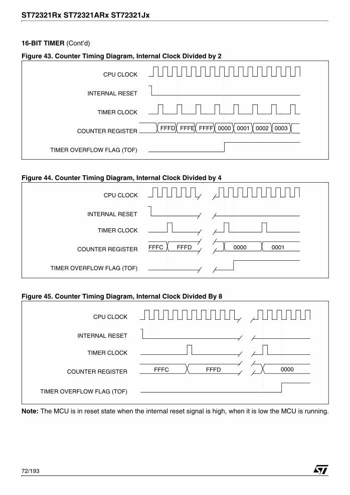
ST72321Rx ST72321ARx ST72321Jx
16-BIT TIMER (Cont’d)
Figure 43. Counter Timing Diagram, Internal Clock Divided by 2
Figure 44. Counter Timing Diagram, Internal Clock Divided by 4
Figure 45. Counter Timing Diagram, Internal Clock Divided By 8
Note: The MCU is in reset state when the internal reset signal is high, when it is low the MCU is running.
CPU CLOCK
FFFD FFFE FFFF 0000 0001 0002 0003
INTERNAL RESET
TIMER CLOCK
COUNTER REGISTER
TIMER OVERFLOW FLAG (TOF)
FFFC FFFD 0000 0001
CPU CLOCK
INTERNAL RESET
TIMER CLOCK
COUNTER REGISTER
TIMER OVERFLOW FLAG (TOF)
CPU CLOCK
INTERNAL RESET
TIMER CLOCK
COUNTER REGISTER
TIMER OVERFLOW FLAG (TOF)
FFFC FFFD 0000
72/193

ST72321Rx ST72321ARx ST72321Jx
16-BIT TIMER (Cont’d)
10.4.3.3 Input CaptureIn this section, the index, i, may be 1 or 2 becausethere are two input capture functions in the 16-bittimer.
The two 16-bit input capture registers (IC1R andIC2R) are used to latch the value of the free run-ning counter after a transition is detected on theICAPi pin (see Figure 5).
ICiR register is a read-only register.
The active transition is software programmablethrough the IEDGi bit of Control Registers (CRi).
Timing resolution is one count of the free runningcounter: (fCPU/CC[1:0]).
Procedure:To use the input capture function select the follow-ing in the CR2 register:
– Select the timer clock (CC[1:0]) (see Table 1).
– Select the edge of the active transition on theICAP2 pin with the IEDG2 bit (the ICAP2 pinmust be configured as floating input or input withpull-up without interrupt if this configuration isavailable).
And select the following in the CR1 register:
– Set the ICIE bit to generate an interrupt after aninput capture coming from either the ICAP1 pinor the ICAP2 pin
– Select the edge of the active transition on theICAP1 pin with the IEDG1 bit (the ICAP1pin mustbe configured as floating input or input with pull-up without interrupt if this configuration is availa-ble).
When an input capture occurs:
– ICFi bit is set.
– The ICiR register contains the value of the freerunning counter on the active transition on theICAPi pin (see Figure 6).
– A timer interrupt is generated if the ICIE bit is setand the I bit is cleared in the CC register. Other-wise, the interrupt remains pending until bothconditions become true.
Clearing the Input Capture interrupt request (thatis, clearing the ICFi bit) is done in two steps:
1. Reading the SR register while the ICFi bit is set.
2. An access (read or write) to the ICiLR register.
Notes: 1. After reading the ICiHR register, transfer of
input capture data is inhibited and ICFi willnever be set until the ICiLR register is alsoread.
2. The ICiR register contains the free runningcounter value which corresponds to the mostrecent input capture.
3. The two input capture functions can be usedtogether even if the timer also uses the two out-put compare functions.
4. In One Pulse mode and PWM mode only InputCapture 2 can be used.
5. The alternate inputs (ICAP1 and ICAP2) arealways directly connected to the timer. So anytransitions on these pins activates the inputcapture function.Moreover if one of the ICAPi pins is configuredas an input and the second one as an output,an interrupt can be generated if the user tog-gles the output pin and if the ICIE bit is set.This can be avoided if the input capture func-tion i is disabled by reading the ICiHR (see note1).
6. The TOF bit can be used with interrupt genera-tion in order to measure events that go beyondthe timer range (FFFFh).
MS Byte LS ByteICiR ICiHR ICiLR
73/193

ST72321Rx ST72321ARx ST72321Jx
16-BIT TIMER (Cont’d)
Figure 46. Input Capture Block Diagram
Figure 47. Input Capture Timing Diagram
ICIE
CC0CC116-BIT FREE RUNNINGCOUNTER
IEDG1
(Control Register 1) CR1
(Control Register 2) CR2
ICF2ICF1 000
(Status Register) SR
IEDG2
ICAP1
ICAP2
EDGE DETECTCIRCUIT2
16-BIT
IC1R RegisterIC2R Register
EDGE DETECTCIRCUIT1
pin
pin
FF01 FF02 FF03
FF03
TIMER CLOCK
COUNTER REGISTER
ICAPi PIN
ICAPi FLAG
ICAPi REGISTER
Note: The rising edge is the active edge.
74/193

ST72321Rx ST72321ARx ST72321Jx
16-BIT TIMER (Cont’d)
10.4.3.4 Output Compare In this section, the index, i, may be 1 or 2 becausethere are two output compare functions in the 16-bit timer.
This function can be used to control an outputwaveform or indicate when a period of time haselapsed.
When a match is found between the Output Com-pare register and the free running counter, the out-put compare function:
– Assigns pins with a programmable value if theOCiE bit is set
– Sets a flag in the status register
– Generates an interrupt if enabled
Two 16-bit registers Output Compare Register 1(OC1R) and Output Compare Register 2 (OC2R)contain the value to be compared to the counterregister each timer clock cycle.
These registers are readable and writable and arenot affected by the timer hardware. A reset eventchanges the OCiR value to 8000h.
Timing resolution is one count of the free runningcounter: (fCPU/CC[1:0]).
Procedure:To use the output compare function, select the fol-lowing in the CR2 register:
– Set the OCiE bit if an output is needed then theOCMPi pin is dedicated to the output compare isignal.
– Select the timer clock (CC[1:0]) (see Table 1).
And select the following in the CR1 register:
– Select the OLVLi bit to applied to the OCMPi pinsafter the match occurs.
– Set the OCIE bit to generate an interrupt if it isneeded.
When a match is found between OCiR registerand CR register:
– OCFi bit is set.
– The OCMPi pin takes OLVLi bit value (OCMPi pin latch is forced low during reset).
– A timer interrupt is generated if the OCIE bit is set in the CR1 register and the I bit is cleared in the CC register (CC).
The OCiR register value required for a specific tim-ing application can be calculated using the follow-ing formula:
Where:
Δt = Output compare period (in seconds)
fCPU = CPU clock frequency (in hertz)
PRESC = Timer prescaler factor (2, 4 or 8 de-pending on CC[1:0] bits, see Table 1)
If the timer clock is an external clock, the formulais:
Where:
Δt = Output compare period (in seconds)
fEXT = External timer clock frequency (in hertz)
Clearing the output compare interrupt request(that is, clearing the OCFi bit) is done by:
1. Reading the SR register while the OCFi bit isset.
2. An access (read or write) to the OCiLR register.
The following procedure is recommended to pre-vent the OCFi bit from being set between the timeit is read and the write to the OCiR register:
– Write to the OCiHR register (further compares are inhibited).
– Read the SR register (first step of the clearance of the OCFi bit, which may be already set).
– Write to the OCiLR register (enables the output compare function and clears the OCFi bit).
MS Byte LS ByteOCiR OCiHR OCiLR
Δ OCiR =Δt * fCPU
PRESC
Δ OCiR = Δt * fEXT
75/193

ST72321Rx ST72321ARx ST72321Jx
16-BIT TIMER (Cont’d)
Notes: 1. After a processor write cycle to the OCiHR reg-
ister, the output compare function is inhibiteduntil the OCiLR register is also written.
2. If the OCiE bit is not set, the OCMPi pin is ageneral I/O port and the OLVLi bit will notappear when a match is found but an interruptcould be generated if the OCIE bit is set.
3. In both internal and external clock modes,OCFi and OCMPi are set while the countervalue equals the OCiR register value (see Fig-ure 8 for an example with fCPU/2 and Figure 9for an example with fCPU/4). This behavior isthe same in OPM or PWM mode.
4. The output compare functions can be used bothfor generating external events on the OCMPipins even if the input capture mode is alsoused.
5. The value in the 16-bit OCiR register and theOLVi bit should be changed after each suc-cessful comparison in order to control an outputwaveform or establish a new elapsed timeout.
Forced Compare Output capabilityWhen the FOLVi bit is set by software, the OLVLibit is copied to the OCMPi pin. The OLVi bit has tobe toggled in order to toggle the OCMPi pin whenit is enabled (OCiE bit = 1). The OCFi bit is thennot set by hardware, and thus no interrupt requestis generated.
The FOLVLi bits have no effect in both One Pulsemode and PWM mode.
Figure 48. Output Compare Block Diagram
OUTPUT COMPARE
16-bit
CIRCUIT
OC1R Register
16 BIT FREE RUNNINGCOUNTER
OC1E CC0CC1OC2E
OLVL1OLVL2OCIE
(Control Register 1) CR1
(Control Register 2) CR2
000OCF2OCF1
(Status Register) SR
16-bit
16-bit
OCMP1
OCMP2
Latch 1
Latch 2
OC2R Register
Pin
Pin
FOLV2 FOLV1
76/193

ST72321Rx ST72321ARx ST72321Jx
16-BIT TIMER (Cont’d)
Figure 49. Output Compare Timing Diagram, fTIMER = fCPU/2
Figure 50. Output Compare Timing Diagram, fTIMER = fCPU/4
INTERNAL CPU CLOCK
TIMER CLOCK
COUNTER REGISTER
OUTPUT COMPARE REGISTER i (OCRi)
OUTPUT COMPARE FLAG i (OCFi)
OCMPi PIN (OLVLi = 1)
2ED3
2ED0 2ED1 2ED2 2ED3 2ED42ECF
INTERNAL CPU CLOCK
TIMER CLOCK
COUNTER REGISTER
OUTPUT COMPARE REGISTER i (OCRi) 2ED3
2ED0 2ED1 2ED2 2ED3 2ED42ECF
OUTPUT COMPARE FLAG i (OCFi)
OCMPi PIN (OLVLi = 1)
77/193

ST72321Rx ST72321ARx ST72321Jx
16-BIT TIMER (Cont’d)
10.4.3.5 One Pulse ModeOne Pulse mode enables the generation of apulse when an external event occurs. This mode isselected via the OPM bit in the CR2 register.
The One Pulse mode uses the Input Capture1function and the Output Compare1 function.
Procedure:To use One Pulse mode:
1. Load the OC1R register with the value corre-sponding to the length of the pulse (see the for-mula in the opposite column).
2. Select the following in the CR1 register:
– Using the OLVL1 bit, select the level to be ap-plied to the OCMP1 pin after the pulse.
– Using the OLVL2 bit, select the level to be ap-plied to the OCMP1 pin during the pulse.
– Select the edge of the active transition on theICAP1 pin with the IEDG1 bit (the ICAP1 pinmust be configured as floating input).
3. Select the following in the CR2 register:
– Set the OC1E bit, the OCMP1 pin is then ded-icated to the Output Compare 1 function.
– Set the OPM bit.
– Select the timer clock CC[1:0] (see Table 1).
Then, on a valid event on the ICAP1 pin, the coun-ter is initialized to FFFCh and OLVL2 bit is loadedon the OCMP1 pin, the ICF1 bit is set and the val-ue FFFDh is loaded in the IC1R register.
Because the ICF1 bit is set when an active edgeoccurs, an interrupt can be generated if the ICIEbit is set.
Clearing the Input Capture interrupt request (thatis, clearing the ICFi bit) is done in two steps:
1. Reading the SR register while the ICFi bit is set.
2. An access (read or write) to the ICiLR register.
The OC1R register value required for a specifictiming application can be calculated using the fol-lowing formula:
Where:t = Pulse period (in seconds)
fCPU = CPU clock frequency (in hertz)
PRESC = Timer prescaler factor (2, 4 or 8 depend-ing on the CC[1:0] bits, see Table 1)
If the timer clock is an external clock the formula is:
Where:
t = Pulse period (in seconds)
fEXT = External timer clock frequency (in hertz)
When the value of the counter is equal to the valueof the contents of the OC1R register, the OLVL1bit is output on the OCMP1 pin, (See Figure 10).
Notes:1. The OCF1 bit cannot be set by hardware in
One Pulse mode but the OCF2 bit can generatean Output Compare interrupt.
2. When the Pulse Width Modulation (PWM) andOne Pulse mode (OPM) bits are both set, thePWM mode is the only active one.
3. If OLVL1 = OLVL2 a continuous signal will beseen on the OCMP1 pin.
4. The ICAP1 pin can not be used to perform inputcapture. The ICAP2 pin can be used to performinput capture (ICF2 can be set and IC2R can beloaded) but the user must take care that thecounter is reset each time a valid edge occurson the ICAP1 pin and ICF1 can also generatesinterrupt if ICIE is set.
5. When One Pulse mode is used OC1R is dedi-cated to this mode. Nevertheless OC2R andOCF2 can be used to indicate a period of timehas been elapsed but cannot generate an out-put waveform because the level OLVL2 is dedi-cated to the One Pulse mode.
event occurs
Counter= OC1R OCMP1 = OLVL1
When
When
on ICAP1
One Pulse mode cycle
OCMP1 = OLVL2
Counter is resetto FFFCh
ICF1 bit is set
ICR1 = Counter
OCiR Value =t * fCPU
PRESC
- 5
OCiR = t * fEXT -5
78/193

ST72321Rx ST72321ARx ST72321Jx
16-BIT TIMER (Cont’d)
Figure 51. One Pulse Mode Timing Example
Figure 52. Pulse Width Modulation Mode Timing Example with 2 Output Compare Functions
Note: On timers with only one Output Compare register, a fixed frequency PWM signal can be generatedusing the output compare and the counter overflow to define the pulse length.
COUNTER FFFC FFFD FFFE 2ED0 2ED1 2ED2
2ED3
FFFC FFFD
OLVL2 OLVL2OLVL1
ICAP1
OCMP1compare1
Note: IEDG1 = 1, OC1R = 2ED0h, OLVL1 = 0, OLVL2 = 1
01F8
01F8 2ED3IC1R
COUNTER 34E2 34E2 FFFC
OLVL2 OLVL2OLVL1OCMP1
compare2 compare1 compare2
Note: OC1R = 2ED0h, OC2R = 34E2, OLVL1 = 0, OLVL2 = 1
FFFC FFFD FFFE 2ED0 2ED1 2ED2
79/193

ST72321Rx ST72321ARx ST72321Jx
16-BIT TIMER (Cont’d)
10.4.3.6 Pulse Width Modulation ModePulse Width Modulation (PWM) mode enables thegeneration of a signal with a frequency and pulselength determined by the value of the OC1R andOC2R registers.
Pulse Width Modulation mode uses the completeOutput Compare 1 function plus the OC2R regis-ter, and so this functionality can not be used whenPWM mode is activated.
In PWM mode, double buffering is implemented onthe output compare registers. Any new values writ-ten in the OC1R and OC2R registers are takeninto account only at the end of the PWM period(OC2) to avoid spikes on the PWM output pin(OCMP1).
ProcedureTo use Pulse Width Modulation mode:
1. Load the OC2R register with the value corre-sponding to the period of the signal using theformula in the opposite column.
2. Load the OC1R register with the value corre-sponding to the period of the pulse if(OLVL1 = 0 and OLVL2 = 1) using the formulain the opposite column.
3. Select the following in the CR1 register:
– Using the OLVL1 bit, select the level to be ap-plied to the OCMP1 pin after a successfulcomparison with the OC1R register.
– Using the OLVL2 bit, select the level to be ap-plied to the OCMP1 pin after a successfulcomparison with the OC2R register.
4. Select the following in the CR2 register:
– Set OC1E bit: the OCMP1 pin is then dedicat-ed to the output compare 1 function.
– Set the PWM bit.
– Select the timer clock (CC[1:0]) (see Table 1).
If OLVL1 = 1 and OLVL2 = 0 the length of the pos-itive pulse is the difference between the OC2R andOC1R registers.
If OLVL1 = OLVL2 a continuous signal will beseen on the OCMP1 pin.
The OCiR register value required for a specific tim-ing application can be calculated using the follow-ing formula:
Where:t = Signal or pulse period (in seconds)
fCPU = CPU clock frequency (in hertz)
PRESC = Timer prescaler factor (2, 4 or 8 depend-ing on CC[1:0] bits, see Table 1)
If the timer clock is an external clock the formula is:
Where:
t = Signal or pulse period (in seconds)
fEXT = External timer clock frequency (in hertz)
The Output Compare 2 event causes the counterto be initialized to FFFCh (See Figure 11)
Notes: 1. After a write instruction to the OCiHR register,
the output compare function is inhibited until theOCiLR register is also written.
2. The OCF1 and OCF2 bits cannot be set byhardware in PWM mode therefore the OutputCompare interrupt is inhibited.
3. The ICF1 bit is set by hardware when the coun-ter reaches the OC2R value and can produce atimer interrupt if the ICIE bit is set and the I bit iscleared.
4. In PWM mode the ICAP1 pin can not be usedto perform input capture because it is discon-nected to the timer. The ICAP2 pin can be usedto perform input capture (ICF2 can be set andIC2R can be loaded) but the user must takecare that the counter is reset each period andICF1 can also generates interrupt if ICIE is set.
5. When the Pulse Width Modulation (PWM) andOne Pulse mode (OPM) bits are both set, thePWM mode is the only active one.
Counter
OCMP1 = OLVL2Counter= OC2R
OCMP1 = OLVL1
When
When
= OC1R
Pulse Width Modulation cycle
Counter is resetto FFFCh
ICF1 bit is set
OCiR Value =t * fCPU
PRESC
- 5
OCiR = t * fEXT -5
80/193

ST72321Rx ST72321ARx ST72321Jx
16-BIT TIMER (Cont’d)
10.4.4 Low Power Modes
10.4.5 Interrupts
Note: The 16-bit Timer interrupt events are connected to the same interrupt vector (see Interrupts chap-ter). These events generate an interrupt if the corresponding Enable Control Bit is set and the interruptmask in the CC register is reset (RIM instruction).
10.4.6 Summary of Timer Modes
1) See note 4 in Section 0.1.3.5 One Pulse Mode
2) See note 5 in Section 0.1.3.5 One Pulse Mode
3) See note 4 in Section 0.1.3.6 Pulse Width Modulation Mode
Mode Description
WAITNo effect on 16-bit Timer. Timer interrupts cause the device to exit from WAIT mode.
HALT
16-bit Timer registers are frozen.
In HALT mode, the counter stops counting until Halt mode is exited. Counting resumes from the previous count when the MCU is woken up by an interrupt with “exit from HALT mode” capability or from the counter reset value when the MCU is woken up by a RESET.
If an input capture event occurs on the ICAPi pin, the input capture detection circuitry is armed. Consequent-ly, when the MCU is woken up by an interrupt with “exit from HALT mode” capability, the ICFi bit is set, and the counter value present when exiting from HALT mode is captured into the ICiR register.
Interrupt EventEventFlag
Enable Control
Bit
Exit fromWait
Exit from Halt
Input Capture 1 event/Counter reset in PWM mode ICF1ICIE
Yes NoInput Capture 2 event ICF2Output Compare 1 event (not available in PWM mode) OCF1
OCIEOutput Compare 2 event (not available in PWM mode) OCF2Timer Overflow event TOF TOIE
MODESTIMER RESOURCES
Input Capture 1 Input Capture 2 Output Compare 1 Output Compare 2Input Capture (1 and/or 2)
Yes Yes Yes YesOutput Compare (1 and/or 2)One Pulse Mode
NoNot Recommended1)
NoPartially 2)
PWM Mode Not Recommended3) No
81/193

ST72321Rx ST72321ARx ST72321Jx
16-BIT TIMER (Cont’d)
10.4.7 Register DescriptionEach Timer is associated with three control andstatus registers, and with six pairs of data registers(16-bit values) relating to the two input captures,the two output compares, the counter and the al-ternate counter.
CONTROL REGISTER 1 (CR1)Read/Write
Reset Value: 0000 0000 (00h)
Bit 7 = ICIE Input Capture Interrupt Enable.0: Interrupt is inhibited.1: A timer interrupt is generated whenever the
ICF1 or ICF2 bit of the SR register is set.
Bit 6 = OCIE Output Compare Interrupt Enable.0: Interrupt is inhibited.1: A timer interrupt is generated whenever the
OCF1 or OCF2 bit of the SR register is set.
Bit 5 = TOIE Timer Overflow Interrupt Enable.0: Interrupt is inhibited.1: A timer interrupt is enabled whenever the TOF
bit of the SR register is set.
Bit 4 = FOLV2 Forced Output Compare 2.This bit is set and cleared by software.0: No effect on the OCMP2 pin.1: Forces the OLVL2 bit to be copied to the
OCMP2 pin, if the OC2E bit is set and even ifthere is no successful comparison.
Bit 3 = FOLV1 Forced Output Compare 1.This bit is set and cleared by software.0: No effect on the OCMP1 pin.1: Forces OLVL1 to be copied to the OCMP1 pin, if
the OC1E bit is set and even if there is no suc-cessful comparison.
Bit 2 = OLVL2 Output Level 2.This bit is copied to the OCMP2 pin whenever asuccessful comparison occurs with the OC2R reg-ister and OCxE is set in the CR2 register. This val-ue is copied to the OCMP1 pin in One Pulse modeand Pulse Width Modulation mode.
Bit 1 = IEDG1 Input Edge 1.This bit determines which type of level transitionon the ICAP1 pin will trigger the capture.0: A falling edge triggers the capture.1: A rising edge triggers the capture.
Bit 0 = OLVL1 Output Level 1.The OLVL1 bit is copied to the OCMP1 pin when-ever a successful comparison occurs with theOC1R register and the OC1E bit is set in the CR2register.
7 0
ICIE OCIE TOIE FOLV2 FOLV1 OLVL2 IEDG1 OLVL1
82/193

ST72321Rx ST72321ARx ST72321Jx
16-BIT TIMER (Cont’d)
CONTROL REGISTER 2 (CR2)Read/Write
Reset Value: 0000 0000 (00h)
Bit 7 = OC1E Output Compare 1 Pin Enable.This bit is used only to output the signal from thetimer on the OCMP1 pin (OLV1 in Output Com-pare mode, both OLV1 and OLV2 in PWM andone-pulse mode). Whatever the value of the OC1Ebit, the Output Compare 1 function of the timer re-mains active.0: OCMP1 pin alternate function disabled (I/O pin
free for general-purpose I/O).1: OCMP1 pin alternate function enabled.
Bit 6 = OC2E Output Compare 2 Pin Enable.This bit is used only to output the signal from thetimer on the OCMP2 pin (OLV2 in Output Com-pare mode). Whatever the value of the OC2E bit,the Output Compare 2 function of the timer re-mains active.0: OCMP2 pin alternate function disabled (I/O pin
free for general-purpose I/O).1: OCMP2 pin alternate function enabled.
Bit 5 = OPM One Pulse Mode.0: One Pulse mode is not active.1: One Pulse mode is active, the ICAP1 pin can be
used to trigger one pulse on the OCMP1 pin; theactive transition is given by the IEDG1 bit. Thelength of the generated pulse depends on thecontents of the OC1R register.
Bit 4 = PWM Pulse Width Modulation.0: PWM mode is not active.1: PWM mode is active, the OCMP1 pin outputs a
programmable cyclic signal; the length of thepulse depends on the value of OC1R register;the period depends on the value of OC2R regis-ter.
Bit 3, 2 = CC[1:0] Clock Control.
The timer clock mode depends on these bits:
Table 17. Clock Control Bits
Note: If the external clock pin is not available, pro-gramming the external clock configuration stopsthe counter.
Bit 1 = IEDG2 Input Edge 2.This bit determines which type of level transitionon the ICAP2 pin will trigger the capture.0: A falling edge triggers the capture.1: A rising edge triggers the capture.
Bit 0 = EXEDG External Clock Edge.This bit determines which type of level transitionon the external clock pin EXTCLK will trigger thecounter register. 0: A falling edge triggers the counter register.1: A rising edge triggers the counter register.
7 0
OC1E OC2E OPM PWM CC1 CC0 IEDG2 EXEDG
Timer Clock CC1 CC0fCPU / 4
00
fCPU / 2 1fCPU / 8
10
External Clock (where available) 1
83/193

ST72321Rx ST72321ARx ST72321Jx
16-BIT TIMER (Cont’d)
CONTROL/STATUS REGISTER (CSR)Read/Write (bits 7:3 read only)
Reset Value: xxxx x0xx (xxh)
Bit 7 = ICF1 Input Capture Flag 1.0: No input capture (reset value).1: An input capture has occurred on the ICAP1 pin
or the counter has reached the OC2R value inPWM mode. To clear this bit, first read the SRregister, then read or write the low byte of theIC1R (IC1LR) register.
Bit 6 = OCF1 Output Compare Flag 1.0: No match (reset value).1: The content of the free running counter has
matched the content of the OC1R register. Toclear this bit, first read the SR register, then reador write the low byte of the OC1R (OC1LR) reg-ister.
Bit 5 = TOF Timer Overflow Flag.0: No timer overflow (reset value).1: The free running counter rolled over from FFFFh
to 0000h. To clear this bit, first read the SR reg-ister, then read or write the low byte of the CR(CLR) register.
Note: Reading or writing the ACLR register doesnot clear TOF.
Bit 4 = ICF2 Input Capture Flag 2.0: No input capture (reset value).1: An input capture has occurred on the ICAP2
pin. To clear this bit, first read the SR register,then read or write the low byte of the IC2R(IC2LR) register.
Bit 3 = OCF2 Output Compare Flag 2.0: No match (reset value).1: The content of the free running counter has
matched the content of the OC2R register. Toclear this bit, first read the SR register, then reador write the low byte of the OC2R (OC2LR) reg-ister.
Bit 2 = TIMD Timer disable.This bit is set and cleared by software. When set, itfreezes the timer prescaler and counter and disa-bled the output functions (OCMP1 and OCMP2pins) to reduce power consumption. Access to thetimer registers is still available, allowing the timerconfiguration to be changed, or the counter reset,while it is disabled.0: Timer enabled1: Timer prescaler, counter and outputs disabled
Bits 1:0 = Reserved, must be kept cleared.
7 0
ICF1 OCF1 TOF ICF2 OCF2 TIMD 0 0
84/193

ST72321Rx ST72321ARx ST72321Jx
16-BIT TIMER (Cont’d)
INPUT CAPTURE 1 HIGH REGISTER (IC1HR)Read OnlyReset Value: Undefined
This is an 8-bit read only register that contains thehigh part of the counter value (transferred by theinput capture 1 event).
INPUT CAPTURE 1 LOW REGISTER (IC1LR)Read OnlyReset Value: Undefined
This is an 8-bit read only register that contains thelow part of the counter value (transferred by the in-put capture 1 event).
OUTPUT COMPARE 1 HIGH REGISTER(OC1HR)Read/WriteReset Value: 1000 0000 (80h)
This is an 8-bit register that contains the high partof the value to be compared to the CHR register.
OUTPUT COMPARE 1 LOW REGISTER(OC1LR)Read/WriteReset Value: 0000 0000 (00h)
This is an 8-bit register that contains the low part ofthe value to be compared to the CLR register.
7 0
MSB LSB
7 0
MSB LSB
7 0
MSB LSB
7 0
MSB LSB
85/193

ST72321Rx ST72321ARx ST72321Jx
16-BIT TIMER (Cont’d)
OUTPUT COMPARE 2 HIGH REGISTER(OC2HR)Read/WriteReset Value: 1000 0000 (80h)
This is an 8-bit register that contains the high partof the value to be compared to the CHR register.
OUTPUT COMPARE 2 LOW REGISTER(OC2LR)Read/WriteReset Value: 0000 0000 (00h)
This is an 8-bit register that contains the low part ofthe value to be compared to the CLR register.
COUNTER HIGH REGISTER (CHR)Read OnlyReset Value: 1111 1111 (FFh)
This is an 8-bit register that contains the high partof the counter value.
COUNTER LOW REGISTER (CLR)Read OnlyReset Value: 1111 1100 (FCh)
This is an 8-bit register that contains the low part ofthe counter value. A write to this register resets thecounter. An access to this register after accessingthe CSR register clears the TOF bit.
ALTERNATE COUNTER HIGH REGISTER(ACHR)Read OnlyReset Value: 1111 1111 (FFh)
This is an 8-bit register that contains the high partof the counter value.
ALTERNATE COUNTER LOW REGISTER(ACLR)Read OnlyReset Value: 1111 1100 (FCh)
This is an 8-bit register that contains the low part ofthe counter value. A write to this register resets thecounter. An access to this register after an accessto CSR register does not clear the TOF bit in theCSR register.
INPUT CAPTURE 2 HIGH REGISTER (IC2HR) Read OnlyReset Value: Undefined
This is an 8-bit read only register that contains thehigh part of the counter value (transferred by theInput Capture 2 event).
INPUT CAPTURE 2 LOW REGISTER (IC2LR)Read OnlyReset Value: Undefined
This is an 8-bit read only register that contains thelow part of the counter value (transferred by the In-put Capture 2 event).
7 0
MSB LSB
7 0
MSB LSB
7 0
MSB LSB
7 0
MSB LSB
7 0
MSB LSB
7 0
MSB LSB
7 0
MSB LSB
7 0
MSB LSB
86/193

ST72321Rx ST72321ARx ST72321Jx
16-BIT TIMER (Cont’d)
Table 18. 16-Bit Timer Register Map and Reset Values
Related DocumentationAN 973: SCI software communications using 16-bit timer
AN 974: Real Time Clock with ST7 Timer OutputCompare
AN 976: Driving a buzzer through the ST7 TimerPWM function
AN1041: Using ST7 PWM signal to generate ana-log input (sinusoid)
AN1046: UART emulation software
AN1078: PWM duty cycle switch implementingtrue 0 or 100 per cent duty cycle
AN1504: Starting a PWM signal directly at highlevel using the ST7 16-Bit timer
Address(Hex.)
RegisterLabel
7 6 5 4 3 2 1 0
Timer A: 32Timer B: 42
CR1Reset Value
ICIE0
OCIE0
TOIE0
FOLV20
FOLV10
OLVL20
IEDG10
OLVL10
Timer A: 31Timer B: 41
CR2Reset Value
OC1E0
OC2E0
OPM0
PWM0
CC10
CC00
IEDG20
EXEDG0
Timer A: 33Timer B: 43
CSRReset Value
ICF1x
OCF1x
TOFx
ICF2x
OCF2x
TIMD0
-x
-x
Timer A: 34Timer B: 44
IC1HRReset Value
MSBx x x x x x x
LSBx
Timer A: 35Timer B: 45
IC1LRReset Value
MSBx x x x x x x
LSBx
Timer A: 36Timer B: 46
OC1HRReset Value
MSB1 0 0 0 0 0 0
LSB0
Timer A: 37Timer B: 47
OC1LRReset Value
MSB0 0 0 0 0 0 0
LSB0
Timer A: 3ETimer B: 4E
OC2HRReset Value
MSB1 0 0 0 0 0 0
LSB0
Timer A: 3FTimer B: 4F
OC2LRReset Value
MSB0 0 0 0 0 0 0
LSB0
Timer A: 38Timer B: 48
CHRReset Value
MSB1 1 1 1 1 1 1
LSB1
Timer A: 39Timer B: 49
CLRReset Value
MSB1 1 1 1 1 1 0
LSB0
Timer A: 3ATimer B: 4A
ACHRReset Value
MSB1 1 1 1 1 1 1
LSB1
Timer A: 3BTimer B: 4B
ACLRReset Value
MSB1 1 1 1 1 1 0
LSB0
Timer A: 3CTimer B: 4C
IC2HRReset Value
MSBx x x x x x x
LSBx
Timer A: 3DTimer B: 4D
IC2LRReset Value
MSBx x x x x x x
LSBx
87/193

ST72321Rx ST72321ARx ST72321Jx
10.5 SERIAL PERIPHERAL INTERFACE (SPI)
10.5.1 Introduction The Serial Peripheral Interface (SPI) allows full-duplex, synchronous, serial communication withexternal devices. An SPI system may consist of amaster and one or more slaves however the SPIinterface can not be a master in a multi-mastersystem.
10.5.2 Main Features ■ Full duplex synchronous transfers (on 3 lines)■ Simplex synchronous transfers (on 2 lines)■ Master or slave operation ■ Six master mode frequencies (fCPU/4 max.)■ fCPU/2 max. slave mode frequency (see note)■ SS Management by software or hardware■ Programmable clock polarity and phase■ End of transfer interrupt flag■ Write collision, Master Mode Fault and Overrun
flags
Note: In slave mode, continuous transmission isnot possible at maximum frequency due to thesoftware overhead for clearing status flags and toinitiate the next transmission sequence.
10.5.3 General DescriptionFigure 53 shows the serial peripheral interface(SPI) block diagram. There are 3 registers:
– SPI Control Register (SPICR)
– SPI Control/Status Register (SPICSR)
– SPI Data Register (SPIDR)
The SPI is connected to external devices through4 pins:
– MISO: Master In / Slave Out data
– MOSI: Master Out / Slave In data
– SCK: Serial Clock out by SPI masters and in-put by SPI slaves
Figure 53. Serial Peripheral Interface Block Diagram
SPIDR
Read Buffer
8-Bit Shift Register
Write
Read
Data/Address Bus
SPI
SPIE SPE MSTR CPHA SPR0SPR1CPOL
SERIAL CLOCKGENERATOR
MOSI
MISO
SS
SCK CONTROL
STATE
SPICR
SPICSR
Interrupt request
MASTERCONTROL
SPR2
07
07
SPIF WCOL MODF 0OVR SSISSMSOD
SODbit
SS1
0
88/193
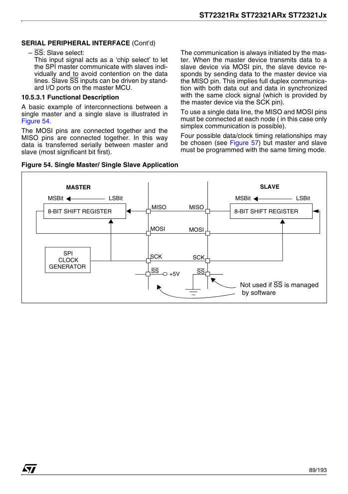
ST72321Rx ST72321ARx ST72321Jx
SERIAL PERIPHERAL INTERFACE (Cont’d)
– SS: Slave select:This input signal acts as a ‘chip select’ to letthe SPI master communicate with slaves indi-vidually and to avoid contention on the datalines. Slave SS inputs can be driven by stand-ard I/O ports on the master MCU.
10.5.3.1 Functional DescriptionA basic example of interconnections between asingle master and a single slave is illustrated inFigure 54.
The MOSI pins are connected together and theMISO pins are connected together. In this waydata is transferred serially between master andslave (most significant bit first).
The communication is always initiated by the mas-ter. When the master device transmits data to aslave device via MOSI pin, the slave device re-sponds by sending data to the master device viathe MISO pin. This implies full duplex communica-tion with both data out and data in synchronizedwith the same clock signal (which is provided bythe master device via the SCK pin).
To use a single data line, the MISO and MOSI pinsmust be connected at each node ( in this case onlysimplex communication is possible).
Four possible data/clock timing relationships maybe chosen (see Figure 57) but master and slavemust be programmed with the same timing mode.
Figure 54. Single Master/ Single Slave Application
8-BIT SHIFT REGISTER
SPICLOCK
GENERATOR
8-BIT SHIFT REGISTERMISO
MOSI MOSI
MISO
SCK SCK
SLAVEMASTER
SS SS+5V
MSBit LSBit MSBit LSBit
Not used if SS is managed by software
89/193

ST72321Rx ST72321ARx ST72321Jx
SERIAL PERIPHERAL INTERFACE (Cont’d)
10.5.3.2 Slave Select ManagementAs an alternative to using the SS pin to control theSlave Select signal, the application can choose tomanage the Slave Select signal by software. Thisis configured by the SSM bit in the SPICSR regis-ter (see Figure 56)
In software management, the external SS pin isfree for other application uses and the internal SSsignal level is driven by writing to the SSI bit in theSPICSR register.
In Master mode:– SS internal must be held high continuously
In Slave Mode:There are two cases depending on the data/clocktiming relationship (see Figure 55):
If CPHA=1 (data latched on 2nd clock edge): – SS internal must be held low during the entire
transmission. This implies that in single slaveapplications the SS pin either can be tied toVSS, or made free for standard I/O by manag-ing the SS function by software (SSM= 1 andSSI=0 in the in the SPICSR register)
If CPHA=0 (data latched on 1st clock edge): – SS internal must be held low during byte
transmission and pulled high between eachbyte to allow the slave to write to the shift reg-ister. If SS is not pulled high, a Write Collisionerror will occur when the slave writes to theshift register (see Section 10.5.5.3).
Figure 55. Generic SS Timing Diagram
Figure 56. Hardware/Software Slave Select Management
MOSI/MISO
Master SS
Slave SS(if CPHA=0)
Slave SS(if CPHA=1)
Byte 1 Byte 2 Byte 3
1
0
SS internal
SSM bit
SSI bit
SS external pin
90/193

ST72321Rx ST72321ARx ST72321Jx
SERIAL PERIPHERAL INTERFACE (Cont’d)
10.5.3.3 Master Mode OperationIn master mode, the serial clock is output on theSCK pin. The clock frequency, polarity and phaseare configured by software (refer to the descriptionof the SPICSR register).
Note: The idle state of SCK must correspond tothe polarity selected in the SPICSR register (bypulling up SCK if CPOL=1 or pulling down SCK ifCPOL=0).
To operate the SPI in master mode, perform thefollowing steps in order (if the SPICSR register isnot written first, the SPICR register setting(MSTR bit) may be not taken into account):1. Write to the SPICR register:
– Select the clock frequency by configuring theSPR[2:0] bits.
– Select the clock polarity and clock phase byconfiguring the CPOL and CPHA bits. Figure57 shows the four possible configurations.Note: The slave must have the same CPOLand CPHA settings as the master.
2. Write to the SPICSR register:– Either set the SSM bit and set the SSI bit or
clear the SSM bit and tie the SS pin high forthe complete byte transmit sequence.
3. Write to the SPICR register:– Set the MSTR and SPE bits
Note: MSTR and SPE bits remain set only ifSS is high).
The transmit sequence begins when softwarewrites a byte in the SPIDR register.
10.5.3.4 Master Mode Transmit SequenceWhen software writes to the SPIDR register, thedata byte is loaded into the 8-bit shift register andthen shifted out serially to the MOSI pin most sig-nificant bit first.
When data transfer is complete:
– The SPIF bit is set by hardware
– An interrupt request is generated if the SPIEbit is set and the interrupt mask in the CCRregister is cleared.
Clearing the SPIF bit is performed by the followingsoftware sequence:
1. An access to the SPICSR register while theSPIF bit is set
2. A read to the SPIDR register.
Note: While the SPIF bit is set, all writes to theSPIDR register are inhibited until the SPICSR reg-ister is read.
10.5.3.5 Slave Mode OperationIn slave mode, the serial clock is received on theSCK pin from the master device.
To operate the SPI in slave mode:
1. Write to the SPICSR register to perform the fol-lowing actions:– Select the clock polarity and clock phase by
configuring the CPOL and CPHA bits (seeFigure 57).Note: The slave must have the same CPOLand CPHA settings as the master.
– Manage the SS pin as described in Section10.5.3.2 and Figure 55. If CPHA=1 SS mustbe held low continuously. If CPHA=0 SS mustbe held low during byte transmission andpulled up between each byte to let the slavewrite in the shift register.
2. Write to the SPICR register to clear the MSTRbit and set the SPE bit to enable the SPI I/Ofunctions.
10.5.3.6 Slave Mode Transmit SequenceWhen software writes to the SPIDR register, thedata byte is loaded into the 8-bit shift register andthen shifted out serially to the MISO pin most sig-nificant bit first.
The transmit sequence begins when the slave de-vice receives the clock signal and the most signifi-cant bit of the data on its MOSI pin.
When data transfer is complete:
– The SPIF bit is set by hardware
– An interrupt request is generated if SPIE bit isset and interrupt mask in the CCR register iscleared.
Clearing the SPIF bit is performed by the followingsoftware sequence:
1. An access to the SPICSR register while theSPIF bit is set.
2. A write or a read to the SPIDR register.
Notes: While the SPIF bit is set, all writes to theSPIDR register are inhibited until the SPICSR reg-ister is read.
The SPIF bit can be cleared during a secondtransmission; however, it must be cleared beforethe second SPIF bit in order to prevent an Overruncondition (see Section 10.5.5.2).
91/193

ST72321Rx ST72321ARx ST72321Jx
SERIAL PERIPHERAL INTERFACE (Cont’d)
10.5.4 Clock Phase and Clock PolarityFour possible timing relationships may be chosenby software, using the CPOL and CPHA bits (SeeFigure 57).
Note: The idle state of SCK must correspond tothe polarity selected in the SPICSR register (bypulling up SCK if CPOL=1 or pulling down SCK ifCPOL=0).
The combination of the CPOL clock polarity andCPHA (clock phase) bits selects the data captureclock edge
Figure 57, shows an SPI transfer with the fourcombinations of the CPHA and CPOL bits. The di-agram may be interpreted as a master or slavetiming diagram where the SCK pin, the MISO pin,the MOSI pin are directly connected between themaster and the slave device.
Note: If CPOL is changed at the communicationbyte boundaries, the SPI must be disabled by re-setting the SPE bit.
Figure 57. Data Clock Timing Diagram
SCK
MSBit Bit 6 Bit 5 Bit 4 Bit3 Bit 2 Bit 1 LSBit
MSBit Bit 6 Bit 5 Bit 4 Bit3 Bit 2 Bit 1 LSBit
MISO(from master)
MOSI(from slave)
SS
(to slave)
CAPTURE STROBE
CPHA =1
MSBit Bit 6 Bit 5 Bit 4 Bit3 Bit 2 Bit 1 LSBit
MSBit Bit 6 Bit 5 Bit 4 Bit3 Bit 2 Bit 1 LSBit
MISO(from master)
MOSI
SS(to slave)
CAPTURE STROBE
CPHA =0
Note: This figure should not be used as a replacement for parametric information.Refer to the Electrical Characteristics chapter.
(from slave)
(CPOL = 1)
SCK(CPOL = 0)
SCK(CPOL = 1)
SCK(CPOL = 0)
92/193
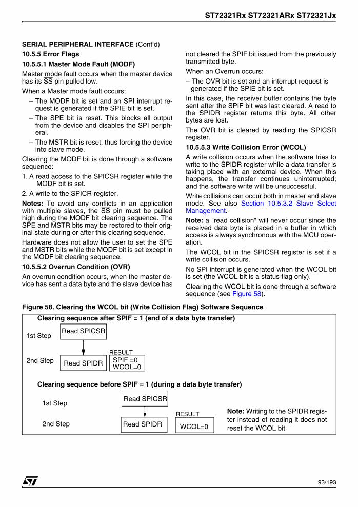
ST72321Rx ST72321ARx ST72321Jx
SERIAL PERIPHERAL INTERFACE (Cont’d)
10.5.5 Error Flags10.5.5.1 Master Mode Fault (MODF)Master mode fault occurs when the master devicehas its SS pin pulled low.
When a Master mode fault occurs:
– The MODF bit is set and an SPI interrupt re-quest is generated if the SPIE bit is set.
– The SPE bit is reset. This blocks all outputfrom the device and disables the SPI periph-eral.
– The MSTR bit is reset, thus forcing the deviceinto slave mode.
Clearing the MODF bit is done through a softwaresequence:
1. A read access to the SPICSR register while theMODF bit is set.
2. A write to the SPICR register.
Notes: To avoid any conflicts in an applicationwith multiple slaves, the SS pin must be pulledhigh during the MODF bit clearing sequence. TheSPE and MSTR bits may be restored to their orig-inal state during or after this clearing sequence.
Hardware does not allow the user to set the SPEand MSTR bits while the MODF bit is set except inthe MODF bit clearing sequence.
10.5.5.2 Overrun Condition (OVR)An overrun condition occurs, when the master de-vice has sent a data byte and the slave device has
not cleared the SPIF bit issued from the previouslytransmitted byte.
When an Overrun occurs:
– The OVR bit is set and an interrupt request is generated if the SPIE bit is set.
In this case, the receiver buffer contains the bytesent after the SPIF bit was last cleared. A read tothe SPIDR register returns this byte. All otherbytes are lost.
The OVR bit is cleared by reading the SPICSRregister.
10.5.5.3 Write Collision Error (WCOL)A write collision occurs when the software tries towrite to the SPIDR register while a data transfer istaking place with an external device. When thishappens, the transfer continues uninterrupted;and the software write will be unsuccessful.
Write collisions can occur both in master and slavemode. See also Section 10.5.3.2 Slave SelectManagement.
Note: a "read collision" will never occur since thereceived data byte is placed in a buffer in whichaccess is always synchronous with the MCU oper-ation.
The WCOL bit in the SPICSR register is set if awrite collision occurs.
No SPI interrupt is generated when the WCOL bitis set (the WCOL bit is a status flag only).
Clearing the WCOL bit is done through a softwaresequence (see Figure 58).
Figure 58. Clearing the WCOL bit (Write Collision Flag) Software Sequence
Clearing sequence after SPIF = 1 (end of a data byte transfer)
1st StepRead SPICSR
Read SPIDR2nd Step SPIF =0WCOL=0
Clearing sequence before SPIF = 1 (during a data byte transfer)
1st Step
2nd Step WCOL=0
Read SPICSR
Read SPIDR
Note: Writing to the SPIDR regis-ter instead of reading it does notreset the WCOL bit
RESULT
RESULT
93/193

ST72321Rx ST72321ARx ST72321Jx
SERIAL PERIPHERAL INTERFACE (Cont’d)
10.5.5.4 Single Master SystemsA typical single master system may be configured,using an MCU as the master and four MCUs asslaves (see Figure 59).
The master device selects the individual slave de-vices by using four pins of a parallel port to controlthe four SS pins of the slave devices.
The SS pins are pulled high during reset since themaster device ports will be forced to be inputs atthat time, thus disabling the slave devices.
Note: To prevent a bus conflict on the MISO linethe master allows only one active slave deviceduring a transmission.
For more security, the slave device may respondto the master with the received data byte. Then themaster will receive the previous byte back from theslave device if all MISO and MOSI pins are con-nected and the slave has not written to its SPIDRregister.
Other transmission security methods can useports for handshake lines or data bytes with com-mand fields.
Figure 59. Single Master / Multiple Slave Configuration
MISO
MOSI
MOSI
MOSI MOSI MOSIMISO MISO MISOMISO
SS
SS SS SS SSSCK SCKSCKSCK
SCK
5V
Por
ts
SlaveMCU
SlaveMCU
SlaveMCU
SlaveMCU
MasterMCU
94/193

ST72321Rx ST72321ARx ST72321Jx
SERIAL PERIPHERAL INTERFACE (Cont’d)
10.5.6 Low Power Modes
10.5.6.1 Using the SPI to wakeup the MCU fromHalt modeIn slave configuration, the SPI is able to wakeupthe ST7 device from HALT mode through a SPIFinterrupt. The data received is subsequently readfrom the SPIDR register when the software is run-ning (interrupt vector fetch). If multiple data trans-fers have been performed before software clearsthe SPIF bit, then the OVR bit is set by hardware.
Note: When waking up from Halt mode, if the SPIremains in Slave mode, it is recommended to per-form an extra communications cycle to bring theSPI from Halt mode state to normal state. If theSPI exits from Slave mode, it returns to normalstate immediately.
Caution: The SPI can wake up the ST7 from Haltmode only if the Slave Select signal (external SSpin or the SSI bit in the SPICSR register) is lowwhen the ST7 enters Halt mode. So if Slave selec-tion is configured as external (see Section10.5.3.2), make sure the master drives a low levelon the SS pin when the slave enters Halt mode.
10.5.7 Interrupts
Note: The SPI interrupt events are connected tothe same interrupt vector (see Interrupts chapter). They generate an interrupt if the correspondingEnable Control Bit is set and the interrupt mask in
Mode Description
WAITNo effect on SPI. SPI interrupt events cause the device to exit from WAIT mode.
HALT
SPI registers are frozen. In HALT mode, the SPI is inactive. SPI oper-ation resumes when the MCU is woken up by an interrupt with “exit from HALT mode” ca-pability. The data received is subsequently read from the SPIDR register when the soft-ware is running (interrupt vector fetching). If several data are received before the wake-up event, then an overrun error is generated. This error can be detected after the fetch of the interrupt routine that woke up the device.
Interrupt Event EventFlag
Enable Control
Bit
Exit fromWait
Exit from Halt
SPI End of Transfer Event
SPIF
SPIE
Yes Yes
Master Mode Fault Event
MODF Yes No
Overrun Error OVR Yes No
95/193

ST72321Rx ST72321ARx ST72321Jx
SERIAL PERIPHERAL INTERFACE (Cont’d)
10.5.8 Register DescriptionCONTROL REGISTER (SPICR)Read/Write
Reset Value: 0000 xxxx (0xh)
Bit 7 = SPIE Serial Peripheral Interrupt Enable.This bit is set and cleared by software.0: Interrupt is inhibited1: An SPI interrupt is generated whenever
SPIF=1, MODF=1 or OVR=1 in the SPICSR register
Bit 6 = SPE Serial Peripheral Output Enable.This bit is set and cleared by software. It is alsocleared by hardware when, in master mode, SS=0(see Section 10.5.5.1 Master Mode Fault(MODF)). The SPE bit is cleared by reset, so theSPI peripheral is not initially connected to the ex-ternal pins.0: I/O pins free for general purpose I/O1: SPI I/O pin alternate functions enabled
Bit 5 = SPR2 Divider Enable.This bit is set and cleared by software and iscleared by reset. It is used with the SPR[1:0] bits toset the baud rate. Refer to Table 19 SPI Mastermode SCK Frequency.0: Divider by 2 enabled1: Divider by 2 disabled
Note: This bit has no effect in slave mode.
Bit 4 = MSTR Master Mode.This bit is set and cleared by software. It is alsocleared by hardware when, in master mode, SS=0(see Section 10.5.5.1 Master Mode Fault(MODF)).0: Slave mode1: Master mode. The function of the SCK pin
changes from an input to an output and the func-tions of the MISO and MOSI pins are reversed.
Bit 3 = CPOL Clock Polarity.This bit is set and cleared by software. This bit de-termines the idle state of the serial Clock. TheCPOL bit affects both the master and slavemodes. 0: SCK pin has a low level idle state 1: SCK pin has a high level idle state
Note: If CPOL is changed at the communicationbyte boundaries, the SPI must be disabled by re-setting the SPE bit.
Bit 2 = CPHA Clock Phase.This bit is set and cleared by software.0: The first clock transition is the first data capture
edge.1: The second clock transition is the first capture
edge.
Note: The slave must have the same CPOL andCPHA settings as the master.
Bits 1:0 = SPR[1:0] Serial Clock Frequency. These bits are set and cleared by software. Usedwith the SPR2 bit, they select the baud rate of theSPI serial clock SCK output by the SPI in mastermode.
Note: These 2 bits have no effect in slave mode.
Table 19. SPI Master mode SCK Frequency
7 0
SPIE SPE SPR2 MSTR CPOL CPHA SPR1 SPR0
Serial Clock SPR2 SPR1 SPR0
fCPU/4 1 0 0
fCPU/8 0 0 0
fCPU/16 0 0 1
fCPU/32 1 1 0
fCPU/64 0 1 0
fCPU/128 0 1 1
96/193

ST72321Rx ST72321ARx ST72321Jx
SERIAL PERIPHERAL INTERFACE (Cont’d)
CONTROL/STATUS REGISTER (SPICSR)Read/Write (some bits Read Only)Reset Value: 0000 0000 (00h)
Bit 7 = SPIF Serial Peripheral Data Transfer Flag(Read only).This bit is set by hardware when a transfer hasbeen completed. An interrupt is generated ifSPIE=1 in the SPICR register. It is cleared by asoftware sequence (an access to the SPICSRregister followed by a write or a read to theSPIDR register).
0: Data transfer is in progress or the flag has been cleared.
1: Data transfer between the device and an exter-nal device has been completed.
Note: While the SPIF bit is set, all writes to theSPIDR register are inhibited until the SPICSR reg-ister is read.
Bit 6 = WCOL Write Collision status (Read only).This bit is set by hardware when a write to theSPIDR register is done during a transmit se-quence. It is cleared by a software sequence (seeFigure 58).0: No write collision occurred1: A write collision has been detected
Bit 5 = OVR SPI Overrun error (Read only).This bit is set by hardware when the byte currentlybeing received in the shift register is ready to betransferred into the SPIDR register while SPIF = 1(See Section 10.5.5.2). An interrupt is generated ifSPIE = 1 in SPICR register. The OVR bit is clearedby software reading the SPICSR register. 0: No overrun error1: Overrun error detected
Bit 4 = MODF Mode Fault flag (Read only).This bit is set by hardware when the SS pin ispulled low in master mode (see Section 10.5.5.1Master Mode Fault (MODF)). An SPI interrupt canbe generated if SPIE=1 in the SPICSR register.This bit is cleared by a software sequence (An ac-cess to the SPICR register while MODF=1 fol-lowed by a write to the SPICR register).0: No master mode fault detected1: A fault in master mode has been detected
Bit 3 = Reserved, must be kept cleared.
Bit 2 = SOD SPI Output Disable.This bit is set and cleared by software. When set, itdisables the alternate function of the SPI output(MOSI in master mode / MISO in slave mode)0: SPI output enabled (if SPE=1)1: SPI output disabled
Bit 1 = SSM SS Management.This bit is set and cleared by software. When set, itdisables the alternate function of the SPI SS pinand uses the SSI bit value instead. See Section10.5.3.2 Slave Select Management.0: Hardware management (SS managed by exter-
nal pin)1: Software management (internal SS signal con-
trolled by SSI bit. External SS pin free for gener-al-purpose I/O)
Bit 0 = SSI SS Internal Mode.This bit is set and cleared by software. It acts as a‘chip select’ by controlling the level of the SS slaveselect signal when the SSM bit is set. 0 : Slave selected1 : Slave deselected
DATA I/O REGISTER (SPIDR)Read/WriteReset Value: Undefined
The SPIDR register is used to transmit and receivedata on the serial bus. In a master device, a writeto this register will initiate transmission/receptionof another byte.
Notes: During the last clock cycle the SPIF bit isset, a copy of the received data byte in the shiftregister is moved to a buffer. When the user readsthe serial peripheral data I/O register, the buffer isactually being read.
While the SPIF bit is set, all writes to the SPIDRregister are inhibited until the SPICSR register isread.
Warning: A write to the SPIDR register placesdata directly into the shift register for transmission.
A read to the SPIDR register returns the value lo-cated in the buffer and not the content of the shiftregister (see Figure 53).
7 0
SPIF WCOL OVR MODF - SOD SSM SSI
7 0
D7 D6 D5 D4 D3 D2 D1 D0
97/193
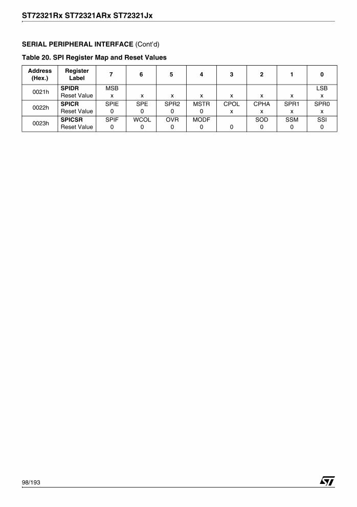
ST72321Rx ST72321ARx ST72321Jx
SERIAL PERIPHERAL INTERFACE (Cont’d)
Table 20. SPI Register Map and Reset Values
Address(Hex.)
RegisterLabel
7 6 5 4 3 2 1 0
0021hSPIDRReset Value
MSBx x x x x x x
LSBx
0022hSPICRReset Value
SPIE0
SPE0
SPR20
MSTR0
CPOLx
CPHAx
SPR1x
SPR0x
0023hSPICSRReset Value
SPIF0
WCOL0
OVR0
MODF0 0
SOD0
SSM0
SSI0
98/193

ST72321Rx ST72321ARx ST72321Jx
10.6 SERIAL COMMUNICATIONS INTERFACE (SCI)
10.6.1 IntroductionThe Serial Communications Interface (SCI) offersa flexible means of full-duplex data exchange withexternal equipment requiring an industry standardNRZ asynchronous serial data format. The SCI of-fers a very wide range of baud rates using twobaud rate generator systems.
10.6.2 Main Features■ Full duplex, asynchronous communications■ NRZ standard format (Mark/Space)■ Dual baud rate generator systems■ Independently programmable transmit and
receive baud rates up to 500K baud■ Programmable data word length (8 or 9 bits)■ Receive buffer full, Transmit buffer empty and
End of Transmission flags■ Two receiver wake-up modes:
– Address bit (MSB)
– Idle line■ Muting function for multiprocessor configurations■ Separate enable bits for Transmitter and
Receiver■ Four error detection flags:
– Overrun error
– Noise error
– Frame error
– Parity error■ Five interrupt sources with flags:
– Transmit data register empty
– Transmission complete
– Receive data register full
– Idle line received
– Overrun error detected■ Parity control:
– Transmits parity bit
– Checks parity of received data byte■ Reduced power consumption mode
10.6.3 General DescriptionThe interface is externally connected to anotherdevice by two pins (see Figure 2.):
– TDO: Transmit Data Output. When the transmit-ter and the receiver are disabled, the output pin returns to its I/O port configuration. When the transmitter and/or the receiver are enabled and nothing is to be transmitted, the TDO pin is at high level.
– RDI: Receive Data Input is the serial data input. Oversampling techniques are used for data re-covery by discriminating between valid incoming data and noise.
Through these pins, serial data is transmitted andreceived as frames comprising:
– An Idle Line prior to transmission or reception
– A start bit
– A data word (8 or 9 bits) least significant bit first
– A Stop bit indicating that the frame is complete
This interface uses two types of baud rate generator:
– A conventional type for commonly-used baud rates
– An extended type with a prescaler offering a very wide range of baud rates even with non-standard oscillator frequencies
99/193

ST72321Rx ST72321ARx ST72321Jx
SERIAL COMMUNICATIONS INTERFACE (Cont’d)
Figure 60. SCI Block Diagram
WAKEUP
UNIT
RECEIVERCONTROL
SR
TRANSMIT
CONTROL
TDRE TC RDRF IDLE OR NF FE PE
SCI
CONTROL
INTERRUPT
CR1
R8 T8 SCID M WAKE PCE PS PIE
Received Data Register (RDR)
Received Shift Register
Read
Transmit Data Register (TDR)
Transmit Shift Register
Write
RDI
TDO
(DATA REGISTER) DR
TRANSMITTER CLOCK
RECEIVER
CLOCK
RECEIVER RATE
TRANSMITTER RATE
BRR
SCP1
fCPU
CONTROL
CONTROL
SCP0 SCT2 SCT1 SCT0 SCR2 SCR1SCR0
/PR/16
CONVENTIONAL BAUD RATE GENERATOR
SBKRWURETEILIERIETCIETIE
CR2
100/193

ST72321Rx ST72321ARx ST72321Jx
SERIAL COMMUNICATIONS INTERFACE (Cont’d)
10.6.4 Functional DescriptionThe block diagram of the Serial Control Interface,is shown in Figure 1. It contains six dedicated reg-isters:
– Two control registers (SCICR1 & SCICR2)
– A status register (SCISR)
– A baud rate register (SCIBRR)
– An extended prescaler receiver register (SCIER-PR)
– An extended prescaler transmitter register (SCI-ETPR)
Refer to the register descriptions in Section 0.1.7for the definitions of each bit.
10.6.4.1 Serial Data FormatWord length may be selected as being either 8 or 9bits by programming the M bit in the SCICR1 reg-ister (see Figure 1.).
The TDO pin is in low state during the start bit.
The TDO pin is in high state during the stop bit.
An Idle character is interpreted as an entire frameof “1”s followed by the start bit of the next framewhich contains data.
A Break character is interpreted on receiving “0”sfor some multiple of the frame period. At the end ofthe last break frame the transmitter inserts an ex-tra “1” bit to acknowledge the start bit.
Transmission and reception are driven by theirown baud rate generator.
Figure 61. Word Length Programming
Bit0 Bit1 Bit2 Bit3 Bit4 Bit5 Bit6 Bit7 Bit8StartBit Stop
Bit
NextStart Bit
Idle Frame
Bit0 Bit1 Bit2 Bit3 Bit4 Bit5 Bit6 Bit7StartBit
StopBit
NextStart Bit
StartBit
Idle FrameStartBit
9-bit Word length (M bit is set)
8-bit Word length (M bit is reset)
PossibleParity
Bit
PossibleParity
Bit
Break Frame StartBit
Extra‘1’
Data Frame
Break Frame StartBit
Extra‘1’
Data Frame
Next Data Frame
Next Data Frame
101/193

ST72321Rx ST72321ARx ST72321Jx
SERIAL COMMUNICATIONS INTERFACE (Cont’d)
10.6.4.2 TransmitterThe transmitter can send data words of either 8 or9 bits depending on the M bit status. When the Mbit is set, word length is 9 bits and the 9th bit (theMSB) has to be stored in the T8 bit in the SCICR1register.
Character TransmissionDuring an SCI transmission, data shifts out leastsignificant bit first on the TDO pin. In this mode,the SCIDR register consists of a buffer (TDR) be-tween the internal bus and the transmit shift regis-ter (see Figure 1.).
Procedure– Select the M bit to define the word length.
– Select the desired baud rate using the SCIBRR and the SCIETPR registers.
– Set the TE bit to assign the TDO pin to the alter-nate function and to send a idle frame as first transmission.
– Access the SCISR register and write the data to send in the SCIDR register (this sequence clears the TDRE bit). Repeat this sequence for each data to be transmitted.
Clearing the TDRE bit is always performed by thefollowing software sequence:
1. An access to the SCISR register
2. A write to the SCIDR register
The TDRE bit is set by hardware and it indicates:
– The TDR register is empty.
– The data transfer is beginning.
– The next data can be written in the SCIDR regis-ter without overwriting the previous data.
This flag generates an interrupt if the TIE bit is setand the I bit is cleared in the CCR register.
When a transmission is taking place, a write in-struction to the SCIDR register stores the data inthe TDR register and which is copied in the shiftregister at the end of the current transmission.
When no transmission is taking place, a write in-struction to the SCIDR register places the data di-rectly in the shift register, the data transmissionstarts, and the TDRE bit is immediately set.
When a frame transmission is complete (after thestop bit) the TC bit is set and an interrupt is gener-ated if the TCIE is set and the I bit is cleared in theCCR register.
Clearing the TC bit is performed by the followingsoftware sequence:
1. An access to the SCISR register
2. A write to the SCIDR register
Note: The TDRE and TC bits are cleared by thesame software sequence.
Break CharactersSetting the SBK bit loads the shift register with abreak character. The break frame length dependson the M bit (see Figure 2.).
As long as the SBK bit is set, the SCI send breakframes to the TDO pin. After clearing this bit bysoftware the SCI insert a logic 1 bit at the end ofthe last break frame to guarantee the recognitionof the start bit of the next frame.
Idle CharactersSetting the TE bit drives the SCI to send an idleframe before the first data frame.
Clearing and then setting the TE bit during a trans-mission sends an idle frame after the current word.
Note: Resetting and setting the TE bit causes thedata in the TDR register to be lost. Therefore thebest time to toggle the TE bit is when the TDRE bitis set, that is, before writing the next byte in theSCIDR.
102/193

ST72321Rx ST72321ARx ST72321Jx
SERIAL COMMUNICATIONS INTERFACE (Cont’d)
10.6.4.3 ReceiverThe SCI can receive data words of either 8 or 9bits. When the M bit is set, word length is 9 bitsand the MSB is stored in the R8 bit in the SCICR1register.
Character receptionDuring a SCI reception, data shifts in least signifi-cant bit first through the RDI pin. In this mode, theSCIDR register consists or a buffer (RDR) be-tween the internal bus and the received shift regis-ter (see Figure 1.).
Procedure– Select the M bit to define the word length.
– Select the desired baud rate using the SCIBRR and the SCIERPR registers.
– Set the RE bit, this enables the receiver which begins searching for a start bit.
When a character is received:
– The RDRF bit is set. It indicates that the content of the shift register is transferred to the RDR.
– An interrupt is generated if the RIE bit is set and the I bit is cleared in the CCR register.
– The error flags can be set if a frame error, noise or an overrun error has been detected during re-ception.
Clearing the RDRF bit is performed by the followingsoftware sequence done by:
1. An access to the SCISR register
2. A read to the SCIDR register.
The RDRF bit must be cleared before the end of thereception of the next character to avoid an overrunerror.
Break CharacterWhen a break character is received, the SCI han-dles it as a framing error.
Idle CharacterWhen a idle frame is detected, there is the sameprocedure as a data received character plus an in-terrupt if the ILIE bit is set and the I bit is cleared inthe CCR register.
Overrun ErrorAn overrun error occurs when a character is re-ceived when RDRF has not been reset. Data cannot be transferred from the shift register to the
RDR register as long as the RDRF bit is notcleared.
When an overrun error occurs:
– The OR bit is set.
– The RDR content is not lost.
– The shift register is overwritten.
– An interrupt is generated if the RIE bit is set and the I bit is cleared in the CCR register.
The OR bit is reset by an access to the SCISR reg-ister followed by a SCIDR register read operation.
Noise ErrorOversampling techniques are used for data recov-ery by discriminating between valid incoming dataand noise. Normal data bits are considered valid ifthree consecutive samples (8th, 9th, 10th) havethe same bit value, otherwise the NF flag is set. Inthe case of start bit detection, the NF flag is set onthe basis of an algorithm combining both validedge detection and three samples (8th, 9th, 10th).Therefore, to prevent the NF flag getting set duringstart bit reception, there should be a valid edge de-tection as well as three valid samples.
When noise is detected in a frame:
– The NF flag is set at the rising edge of the RDRF bit.
– Data is transferred from the Shift register to the SCIDR register.
– No interrupt is generated. However this bit rises at the same time as the RDRF bit which itself generates an interrupt.
The NF flag is reset by a SCISR register read op-eration followed by a SCIDR register read opera-tion.
During reception, if a false start bit is detected (e.g.8th, 9th, 10th samples are 011,101,110), theframe is discarded and the receiving sequence isnot started for this frame. There is no RDRF bit setfor this frame and the NF flag is set internally (notaccessible to the user). This NF flag is accessiblealong with the RDRF bit when a next valid frame isreceived.
Note: If the application Start Bit is not long enoughto match the above requirements, then the NFFlag may get set due to the short Start Bit. In thiscase, the NF flag may be ignored by the applica-tion software when the first valid byte is received.
See also Section 0.1.4.10 .
103/193

ST72321Rx ST72321ARx ST72321Jx
SERIAL COMMUNICATIONS INTERFACE (Cont’d)
Figure 62. SCI Baud Rate and Extended Prescaler Block Diagram
TRANSMITTER
RECEIVER
SCIETPR
SCIERPR
EXTENDED PRESCALER RECEIVER RATE CONTROL
EXTENDED PRESCALER TRANSMITTER RATE CONTROL
EXTENDED PRESCALER
CLOCK
CLOCK
RECEIVER RATE
TRANSMITTER RATE
SCIBRR
SCP1
fCPU
CONTROL
CONTROL
SCP0 SCT2 SCT1 SCT0 SCR2 SCR1SCR0
/PR/16
CONVENTIONAL BAUD RATE GENERATOR
EXTENDED RECEIVER PRESCALER REGISTER
EXTENDED TRANSMITTER PRESCALER REGISTER
104/193
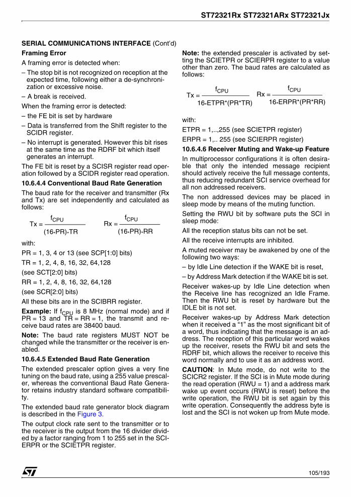
ST72321Rx ST72321ARx ST72321Jx
SERIAL COMMUNICATIONS INTERFACE (Cont’d)
Framing ErrorA framing error is detected when:
– The stop bit is not recognized on reception at the expected time, following either a de-synchroni-zation or excessive noise.
– A break is received.
When the framing error is detected:
– the FE bit is set by hardware
– Data is transferred from the Shift register to the SCIDR register.
– No interrupt is generated. However this bit rises at the same time as the RDRF bit which itself generates an interrupt.
The FE bit is reset by a SCISR register read oper-ation followed by a SCIDR register read operation.
10.6.4.4 Conventional Baud Rate GenerationThe baud rate for the receiver and transmitter (Rxand Tx) are set independently and calculated asfollows:
with:
PR = 1, 3, 4 or 13 (see SCP[1:0] bits)
TR = 1, 2, 4, 8, 16, 32, 64,128
(see SCT[2:0] bits)
RR = 1, 2, 4, 8, 16, 32, 64,128
(see SCR[2:0] bits)
All these bits are in the SCIBRR register.
Example: If fCPU is 8 MHz (normal mode) and ifPR = 13 and TR = RR = 1, the transmit and re-ceive baud rates are 38400 baud.
Note: The baud rate registers MUST NOT bechanged while the transmitter or the receiver is en-abled.
10.6.4.5 Extended Baud Rate GenerationThe extended prescaler option gives a very finetuning on the baud rate, using a 255 value prescal-er, whereas the conventional Baud Rate Genera-tor retains industry standard software compatibili-ty.
The extended baud rate generator block diagramis described in the Figure 3.
The output clock rate sent to the transmitter or tothe receiver is the output from the 16 divider divid-ed by a factor ranging from 1 to 255 set in the SCI-ERPR or the SCIETPR register.
Note: the extended prescaler is activated by set-ting the SCIETPR or SCIERPR register to a valueother than zero. The baud rates are calculated asfollows:
with:
ETPR = 1,..,255 (see SCIETPR register)
ERPR = 1,.. 255 (see SCIERPR register)
10.6.4.6 Receiver Muting and Wake-up FeatureIn multiprocessor configurations it is often desira-ble that only the intended message recipientshould actively receive the full message contents,thus reducing redundant SCI service overhead forall non addressed receivers.
The non addressed devices may be placed insleep mode by means of the muting function.
Setting the RWU bit by software puts the SCI insleep mode:
All the reception status bits can not be set.
All the receive interrupts are inhibited.
A muted receiver may be awakened by one of thefollowing two ways:
– by Idle Line detection if the WAKE bit is reset,
– by Address Mark detection if the WAKE bit is set.
Receiver wakes-up by Idle Line detection whenthe Receive line has recognized an Idle Frame.Then the RWU bit is reset by hardware but theIDLE bit is not set.
Receiver wakes-up by Address Mark detectionwhen it received a “1” as the most significant bit ofa word, thus indicating that the message is an ad-dress. The reception of this particular word wakesup the receiver, resets the RWU bit and sets theRDRF bit, which allows the receiver to receive thisword normally and to use it as an address word.
CAUTION: In Mute mode, do not write to theSCICR2 register. If the SCI is in Mute mode duringthe read operation (RWU = 1) and a address markwake up event occurs (RWU is reset) before thewrite operation, the RWU bit is set again by thiswrite operation. Consequently the address byte islost and the SCI is not woken up from Mute mode.
Tx = (16*PR)*TR
fCPURx =
(16*PR)*RR
fCPU
Tx = 16*ETPR*(PR*TR)
fCPU Rx = 16*ERPR*(PR*RR)
fCPU
105/193

ST72321Rx ST72321ARx ST72321Jx
SERIAL COMMUNICATIONS INTERFACE (Cont’d)
10.6.4.7 Parity ControlParity control (generation of parity bit in transmis-sion and parity checking in reception) can be ena-bled by setting the PCE bit in the SCICR1 register.Depending on the frame length defined by the Mbit, the possible SCI frame formats are as listed inTable 1.
Table 21. Frame Formats
Legend: SB = Start Bit, STB = Stop Bit, PB = Parity Bit
Note: In case of wake up by an address mark, theMSB bit of the data is taken into account and notthe parity bit
Even parity: the parity bit is calculated to obtainan even number of “1s” inside the frame made ofthe 7 or 8 LSB bits (depending on whether M isequal to 0 or 1) and the parity bit.
Example: data = 00110101; 4 bits set => parity bitis 0 if even parity is selected (PS bit = 0).
Odd parity: the parity bit is calculated to obtain anodd number of “1s” inside the frame made of the 7or 8 LSB bits (depending on whether M is equal to0 or 1) and the parity bit.
Example: data = 00110101; 4 bits set => parity bitis 1 if odd parity is selected (PS bit = 1).
Transmission mode: If the PCE bit is set then theMSB bit of the data written in the data register isnot transmitted but is changed by the parity bit.
Reception mode: If the PCE bit is set then the in-terface checks if the received data byte has an
even number of “1s” if even parity is selected(PS = 0) or an odd number of “1s” if odd parity isselected (PS = 1). If the parity check fails, the PEflag is set in the SCISR register and an interrupt isgenerated if PIE is set in the SCICR1 register.
10.6.4.8 SCI Clock ToleranceDuring reception, each bit is sampled 16 times.The majority of the 8th, 9th and 10th samples isconsidered as the bit value. For a valid bit detec-tion, all the three samples should have the samevalue otherwise the noise flag (NF) is set. For ex-ample: If the 8th, 9th and 10th samples are 0, 1and 1 respectively, then the bit value is “1”, but theNoise Flag bit is set because the three samplesvalues are not the same.
Consequently, the bit length must be long enoughso that the 8th, 9th and 10th samples have the de-sired bit value. This means the clock frequencyshould not vary more than 6/16 (37.5%) within onebit. The sampling clock is resynchronized at eachstart bit, so that when receiving 10 bits (one startbit, 1 data byte, 1 stop bit), the clock deviationmust not exceed 3.75%.
Note: The internal sampling clock of the microcon-troller samples the pin value on every falling edge.Therefore, the internal sampling clock and the timethe application expects the sampling to take placemay be out of sync. For example: If the baud rateis 15.625 Kbaud (bit length is 64µs), then the 8th,9th and 10th samples are at 28µs, 32µs and 36µsrespectively (the first sample starting ideally at0µs). But if the falling edge of the internal clock oc-curs just before the pin value changes, the sam-ples would then be out of sync by ~4us. Thismeans the entire bit length must be at least 40µs(36µs for the 10th sample + 4µs for synchroniza-tion with the internal sampling clock).
M bit PCE bit SCI frame0 0 | SB | 8 bit data | STB |0 1 | SB | 7-bit data | PB | STB |1 0 | SB | 9-bit data | STB |1 1 | SB | 8-bit data PB | STB |
106/193

ST72321Rx ST72321ARx ST72321Jx
SERIAL COMMUNICATIONS INTERFACE (Cont’d)
10.6.4.9 Clock Deviation CausesThe causes which contribute to the total deviationare:
– DTRA: Deviation due to transmitter error (Localoscillator error of the transmitter or the trans-mitter is transmitting at a different baud rate).
– DQUANT: Error due to the baud rate quantiza-tion of the receiver.
– DREC: Deviation of the local oscillator of thereceiver: This deviation can occur during thereception of one complete SCI message as-suming that the deviation has been compen-sated at the beginning of the message.
– DTCL: Deviation due to the transmission line(generally due to the transceivers)
All the deviations of the system should be addedand compared to the SCI clock tolerance:
DTRA + DQUANT + DREC + DTCL < 3.75%
10.6.4.10 Noise Error CausesSee also description of Noise error in Section0.1.4.3 .
Start bitThe noise flag (NF) is set during start bit receptionif one of the following conditions occurs:
1. A valid falling edge is not detected. A fallingedge is considered to be valid if the 3 consecu-tive samples before the falling edge occurs aredetected as '1' and, after the falling edgeoccurs, during the sampling of the 16 samples,if one of the samples numbered 3, 5 or 7 isdetected as a “1”.
2. During sampling of the 16 samples, if one of thesamples numbered 8, 9 or 10 is detected as a“1”.
Therefore, a valid Start Bit must satisfy both theabove conditions to prevent the Noise Flag gettingset.
Data Bits The noise flag (NF) is set during normal data bit re-ception if the following condition occurs:
– During the sampling of 16 samples, if all three samples numbered 8, 9 and10 are not the same. The majority of the 8th, 9th and 10th samples is considered as the bit value.
Therefore, a valid Data Bit must have samples 8, 9and 10 at the same value to prevent the NoiseFlag getting set.
Figure 63. Bit Sampling in Reception Mode
RDI LINE
Sample clock 1 2 3 4 5 6 7 8 9 10 11 12 13 14 15 16
sampled values
One bit time
6/16
7/16 7/16
107/193

ST72321Rx ST72321ARx ST72321Jx
SERIAL COMMUNICATIONS INTERFACE (Cont’d)
10.6.5 Low Power Modes 10.6.6 InterruptsThe SCI interrupt events are connected to thesame interrupt vector.
These events generate an interrupt if the corre-sponding Enable Control Bit is set and the inter-rupt mask in the CC register is reset (RIM instruc-tion).
Mode Description
WAITNo effect on SCI.
SCI interrupts cause the device to exit from Wait mode.
HALTSCI registers are frozen.
In Halt mode, the SCI stops transmitting/re-ceiving until Halt mode is exited.
Interrupt EventEventFlag
Enable Control
Bit
Exit fromWait
Exit from Halt
Transmit Data Register Empty
TDRE TIE Yes No
Transmission Com-plete
TC TCIE Yes No
Received Data Ready to be Read
RDRFRIE
Yes No
Overrun Error Detect-ed
OR Yes No
Idle Line Detected IDLE ILIE Yes No Parity Error PE PIE Yes No
108/193
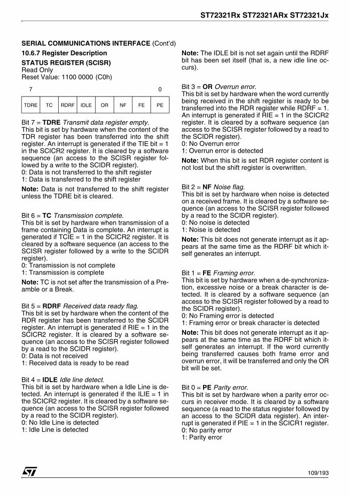
ST72321Rx ST72321ARx ST72321Jx
SERIAL COMMUNICATIONS INTERFACE (Cont’d)
10.6.7 Register DescriptionSTATUS REGISTER (SCISR)Read OnlyReset Value: 1100 0000 (C0h)
Bit 7 = TDRE Transmit data register empty.This bit is set by hardware when the content of theTDR register has been transferred into the shiftregister. An interrupt is generated if the TIE bit = 1in the SCICR2 register. It is cleared by a softwaresequence (an access to the SCISR register fol-lowed by a write to the SCIDR register).0: Data is not transferred to the shift register1: Data is transferred to the shift register
Note: Data is not transferred to the shift registerunless the TDRE bit is cleared.
Bit 6 = TC Transmission complete.This bit is set by hardware when transmission of aframe containing Data is complete. An interrupt isgenerated if TCIE = 1 in the SCICR2 register. It iscleared by a software sequence (an access to theSCISR register followed by a write to the SCIDRregister).0: Transmission is not complete1: Transmission is complete
Note: TC is not set after the transmission of a Pre-amble or a Break.
Bit 5 = RDRF Received data ready flag.This bit is set by hardware when the content of theRDR register has been transferred to the SCIDRregister. An interrupt is generated if RIE = 1 in theSCICR2 register. It is cleared by a software se-quence (an access to the SCISR register followedby a read to the SCIDR register).0: Data is not received1: Received data is ready to be read
Bit 4 = IDLE Idle line detect. This bit is set by hardware when a Idle Line is de-tected. An interrupt is generated if the ILIE = 1 inthe SCICR2 register. It is cleared by a software se-quence (an access to the SCISR register followedby a read to the SCIDR register).0: No Idle Line is detected1: Idle Line is detected
Note: The IDLE bit is not set again until the RDRFbit has been set itself (that is, a new idle line oc-curs).
Bit 3 = OR Overrun error.This bit is set by hardware when the word currentlybeing received in the shift register is ready to betransferred into the RDR register while RDRF = 1.An interrupt is generated if RIE = 1 in the SCICR2register. It is cleared by a software sequence (anaccess to the SCISR register followed by a read tothe SCIDR register).0: No Overrun error 1: Overrun error is detected
Note: When this bit is set RDR register content isnot lost but the shift register is overwritten.
Bit 2 = NF Noise flag. This bit is set by hardware when noise is detectedon a received frame. It is cleared by a software se-quence (an access to the SCISR register followedby a read to the SCIDR register).0: No noise is detected1: Noise is detected
Note: This bit does not generate interrupt as it ap-pears at the same time as the RDRF bit which it-self generates an interrupt.
Bit 1 = FE Framing error.This bit is set by hardware when a de-synchroniza-tion, excessive noise or a break character is de-tected. It is cleared by a software sequence (anaccess to the SCISR register followed by a read tothe SCIDR register).0: No Framing error is detected1: Framing error or break character is detected
Note: This bit does not generate interrupt as it ap-pears at the same time as the RDRF bit which it-self generates an interrupt. If the word currentlybeing transferred causes both frame error andoverrun error, it will be transferred and only the ORbit will be set.
Bit 0 = PE Parity error.This bit is set by hardware when a parity error oc-curs in receiver mode. It is cleared by a softwaresequence (a read to the status register followed byan access to the SCIDR data register). An inter-rupt is generated if PIE = 1 in the SCICR1 register.0: No parity error1: Parity error
7 0
TDRE TC RDRF IDLE OR NF FE PE
109/193

ST72321Rx ST72321ARx ST72321Jx
SERIAL COMMUNICATIONS INTERFACE (Cont’d)
CONTROL REGISTER 1 (SCICR1)Read/Write
Reset Value: x000 0000 (x0h)
Bit 7 = R8 Receive data bit 8.This bit is used to store the 9th bit of the receivedword when M = 1.
Bit 6 = T8 Transmit data bit 8.This bit is used to store the 9th bit of the transmit-ted word when M = 1.
Bit 5 = SCID Disabled for low power consumptionWhen this bit is set the SCI prescalers and outputsare stopped and the end of the current byte trans-fer in order to reduce power consumption.This bitis set and cleared by software.0: SCI enabled1: SCI prescaler and outputs disabled
Bit 4 = M Word length.This bit determines the word length. It is set orcleared by software.0: 1 Start bit, 8 Data bits, 1 Stop bit 1: 1 Start bit, 9 Data bits, 1 Stop bit
Note: The M bit must not be modified during a datatransfer (both transmission and reception).
Bit 3 = WAKE Wake-Up method.This bit determines the SCI Wake-Up method, it isset or cleared by software.0: Idle Line1: Address Mark
Bit 2 = PCE Parity control enable.This bit selects the hardware parity control (gener-ation and detection). When the parity control is en-abled, the computed parity is inserted at the MSBposition (9th bit if M = 1; 8th bit if M = 0) and parityis checked on the received data. This bit is set andcleared by software. Once it is set, PCE is activeafter the current byte (in reception and in transmis-sion).0: Parity control disabled1: Parity control enabled
Bit 1 = PS Parity selection.This bit selects the odd or even parity when theparity generation/detection is enabled (PCE bitset). It is set and cleared by software. The parity isselected after the current byte.0: Even parity1: Odd parity
Bit 0 = PIE Parity interrupt enable.This bit enables the interrupt capability of the hard-ware parity control when a parity error is detected(PE bit set). It is set and cleared by software.0: Parity error interrupt disabled1: Parity error interrupt enabled.
7 0
R8 T8 SCID M WAKE PCE PS PIE
110/193

ST72321Rx ST72321ARx ST72321Jx
SERIAL COMMUNICATIONS INTERFACE (Cont’d)
CONTROL REGISTER 2 (SCICR2)Read/Write
Reset Value: 0000 0000 (00h)
Bit 7 = TIE Transmitter interrupt enable.This bit is set and cleared by software.0: Interrupt is inhibited1: An SCI interrupt is generated whenever
TDRE=1 in the SCISR register
Bit 6 = TCIE Transmission complete interrupt ena-ble This bit is set and cleared by software.0: Interrupt is inhibited1: An SCI interrupt is generated whenever TC=1 in
the SCISR register
Bit 5 = RIE Receiver interrupt enable. This bit is set and cleared by software.0: Interrupt is inhibited1: An SCI interrupt is generated whenever OR=1
or RDRF=1 in the SCISR register
Bit 4 = ILIE Idle line interrupt enable. This bit is set and cleared by software.0: Interrupt is inhibited1: An SCI interrupt is generated whenever IDLE=1
in the SCISR register.
Bit 3 = TE Transmitter enable. This bit enables the transmitter. It is set andcleared by software. 0: Transmitter is disabled1: Transmitter is enabled
Notes: – During transmission, a “0” pulse on the TE bit
(“0” followed by “1”) sends a preamble (idle line) after the current word.
– When TE is set there is a 1 bit-time delay before the transmission starts.
CAUTION: The TDO pin is free for general pur-pose I/O only when the TE and RE bits are bothcleared (or if TE is never set).
Bit 2 = RE Receiver enable.This bit enables the receiver. It is set and clearedby software. 0: Receiver is disabled1: Receiver is enabled and begins searching for a
start bit
Bit 1 = RWU Receiver wake-up.This bit determines if the SCI is in mute mode ornot. It is set and cleared by software and can becleared by hardware when a wake-up sequence isrecognized.0: Receiver in Active mode1: Receiver in Mute mode
Note: Before selecting Mute mode (setting theRWU bit), the SCI must receive some data first,otherwise it cannot function in Mute mode withwake-up by idle line detection.
Bit 0 = SBK Send break.This bit set is used to send break characters. It isset and cleared by software.0: No break character is transmitted1: Break characters are transmitted
Note: If the SBK bit is set to “1” and then to “0”, thetransmitter sends a BREAK word at the end of thecurrent word.
7 0
TIE TCIE RIE ILIE TE RE RWU SBK
111/193

ST72321Rx ST72321ARx ST72321Jx
SERIAL COMMUNICATIONS INTERFACE (Cont’d)
DATA REGISTER (SCIDR)Read/Write
Reset Value: Undefined
Contains the Received or Transmitted data char-acter, depending on whether it is read from or writ-ten to.
The Data register performs a double function (readand write) since it is composed of two registers,one for transmission (TDR) and one for reception(RDR).The TDR register provides the parallel interfacebetween the internal bus and the output shift reg-ister (see Figure 1.).The RDR register provides the parallel interfacebetween the input shift register and the internalbus (see Figure 1.).
BAUD RATE REGISTER (SCIBRR)Read/Write
Reset Value: 0000 0000 (00h)
Bits 7:6 = SCP[1:0] First SCI Prescaler These 2 prescaling bits allow several standardclock division ranges:
Bits 5:3 = SCT[2:0] SCI Transmitter rate divisorThese 3 bits, in conjunction with the SCP1 & SCP0bits define the total division applied to the busclock to yield the transmit rate clock in convention-al Baud Rate Generator mode.
Bits 2:0 = SCR[2:0] SCI Receiver rate divisor.These 3 bits, in conjunction with the SCP[1:0] bitsdefine the total division applied to the bus clock toyield the receive rate clock in conventional BaudRate Generator mode.
7 0
DR7 DR6 DR5 DR4 DR3 DR2 DR1 DR0
7 0
SCP1 SCP0 SCT2 SCT1 SCT0 SCR2 SCR1 SCR0
PR Prescaling factor SCP1 SCP0
1 0 0
3 0 1
4 1 0
13 1 1
TR dividing factor SCT2 SCT1 SCT0
1 0 0 0
2 0 0 1
4 0 1 0
8 0 1 1
16 1 0 0
32 1 0 1
64 1 1 0
128 1 1 1
RR Dividing factor SCR2 SCR1 SCR0
1 0 0 0
2 0 0 1
4 0 1 0
8 0 1 1
16 1 0 0
32 1 0 1
64 1 1 0
128 1 1 1
112/193

ST72321Rx ST72321ARx ST72321Jx
SERIAL COMMUNICATIONS INTERFACE (Cont’d)
EXTENDED RECEIVE PRESCALER DIVISIONREGISTER (SCIERPR)Read/Write
Reset Value: 0000 0000 (00h)
Allows setting of the Extended Prescaler rate divi-sion factor for the receive circuit.
Bits 7:0 = ERPR[7:0] 8-bit Extended ReceivePrescaler Register.
The extended Baud Rate Generator is activatedwhen a value different from 00h is stored in thisregister. Therefore the clock frequency issuedfrom the 16 divider (see Figure 3.) is divided by thebinary factor set in the SCIERPR register (in therange 1 to 255).
The extended baud rate generator is not used af-ter a reset.
EXTENDED TRANSMIT PRESCALER DIVISIONREGISTER (SCIETPR)Read/Write
Reset Value:0000 0000 (00h)
Allows setting of the External Prescaler rate divi-sion factor for the transmit circuit.
Bits 7:0 = ETPR[7:0] 8-bit Extended TransmitPrescaler Register.
The extended Baud Rate Generator is activatedwhen a value different from 00h is stored in thisregister. Therefore the clock frequency issuedfrom the 16 divider (see Figure 3.) is divided by thebinary factor set in the SCIETPR register (in therange 1 to 255).
The extended baud rate generator is not used af-ter a reset.
Table 22. Baudrate Selection
7 0
ERPR7
ERPR6
ERPR5
ERPR4
ERPR3
ERPR2
ERPR1
ERPR0
7 0
ETPR7
ETPR6
ETPR5
ETPR4
ETPR3
ETPR2
ETPR1
ETPR0
Symbol ParameterConditions
StandardBaudRate
UnitfCPU
Accuracy vs Standard
Prescaler
fTx
fRxCommunication frequency 8 MHz
~0.16%
Conventional ModeTR (or RR)=128, PR=13TR (or RR)= 32, PR=13TR (or RR)= 16, PR=13TR (or RR)= 8, PR=13TR (or RR)= 4, PR=13TR (or RR)= 16, PR= 3TR (or RR)= 2, PR=13TR (or RR)= 1, PR=13
3001200240048009600
104001920038400
~300.48~1201.92~2403.84~4807.69~9615.38
~10416.67~19230.77~38461.54
Hz
~0.79%Extended ModeETPR (or ERPR) = 35, TR (or RR)= 1, PR=1
14400 ~14285.71
113/193
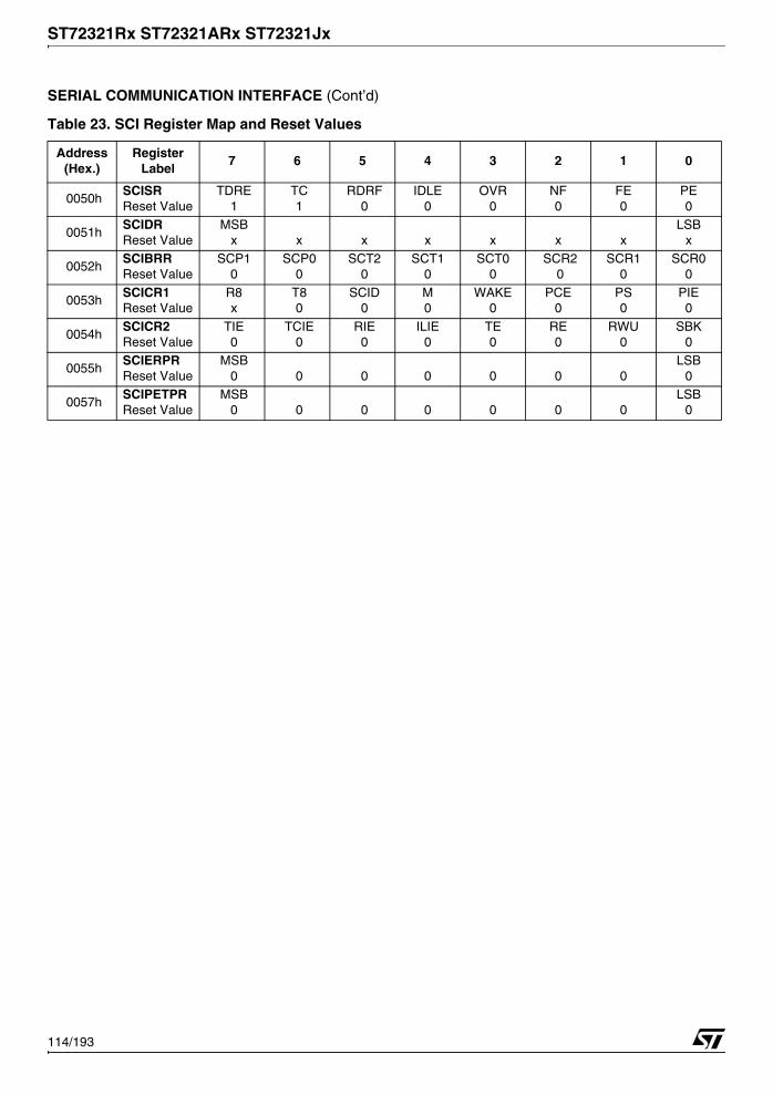
ST72321Rx ST72321ARx ST72321Jx
SERIAL COMMUNICATION INTERFACE (Cont’d)
Table 23. SCI Register Map and Reset Values
Address(Hex.)
RegisterLabel
7 6 5 4 3 2 1 0
0050hSCISRReset Value
TDRE1
TC1
RDRF0
IDLE0
OVR0
NF0
FE0
PE0
0051hSCIDRReset Value
MSBx x x x x x x
LSBx
0052hSCIBRRReset Value
SCP10
SCP00
SCT20
SCT10
SCT00
SCR20
SCR10
SCR00
0053hSCICR1Reset Value
R8x
T80
SCID0
M0
WAKE0
PCE0
PS0
PIE0
0054hSCICR2Reset Value
TIE0
TCIE0
RIE0
ILIE0
TE0
RE0
RWU0
SBK0
0055hSCIERPRReset Value
MSB0 0 0 0 0 0 0
LSB0
0057hSCIPETPRReset Value
MSB0 0 0 0 0 0 0
LSB0
114/193

ST72321Rx ST72321ARx ST72321Jx
10.7 I2C BUS INTERFACE (I2C)
10.7.1 IntroductionThe I2C Bus Interface serves as an interface be-tween the microcontroller and the serial I2C bus. Itprovides both multimaster and slave functions,and controls all I2C bus-specific sequencing, pro-tocol, arbitration and timing. It supports fast I2Cmode (400kHz).
10.7.2 Main Features■ Parallel-bus/I2C protocol converter■ Multi-master capability■ 7-bit/10-bit Addressing■ SMBus V1.1 Compliant■ Transmitter/Receiver flag■ End-of-byte transmission flag■ Transfer problem detection
I2C Master Features:■ Clock generation■ I2C bus busy flag■ Arbitration Lost Flag■ End of byte transmission flag■ Transmitter/Receiver Flag■ Start bit detection flag■ Start and Stop generation
I2C Slave Features:■ Stop bit detection■ I2C bus busy flag■ Detection of misplaced start or stop condition■ Programmable I2C Address detection ■ Transfer problem detection ■ End-of-byte transmission flag■ Transmitter/Receiver flag
10.7.3 General DescriptionIn addition to receiving and transmitting data, thisinterface converts it from serial to parallel format
and vice versa, using either an interrupt or polledhandshake. The interrupts are enabled or disabledby software. The interface is connected to the I2Cbus by a data pin (SDAI) and by a clock pin (SCLI).It can be connected both with a standard I2C busand a Fast I2C bus. This selection is made by soft-ware.
Mode SelectionThe interface can operate in the four followingmodes:
– Slave transmitter/receiver
– Master transmitter/receiver
By default, it operates in slave mode.
The interface automatically switches from slave tomaster after it generates a START condition andfrom master to slave in case of arbitration loss or aSTOP generation, allowing then Multi-Master ca-pability.
Communication FlowIn Master mode, it initiates a data transfer andgenerates the clock signal. A serial data transferalways begins with a start condition and ends witha stop condition. Both start and stop conditions aregenerated in master mode by software.
In Slave mode, the interface is capable of recog-nising its own address (7 or 10-bit), and the Gen-eral Call address. The General Call address de-tection may be enabled or disabled by software.
Data and addresses are transferred as 8-bit bytes,MSB first. The first byte(s) following the start con-dition contain the address (one in 7-bit mode, twoin 10-bit mode). The address is always transmittedin Master mode.
A 9th clock pulse follows the 8 clock cycles of abyte transfer, during which the receiver must sendan acknowledge bit to the transmitter. Refer to Fig-ure 64.
Figure 64. I2C BUS Protocol
SCL
SDA
1 2 8 9
MSB ACK
STOP STARTCONDITIONCONDITION
VR02119B
115/193
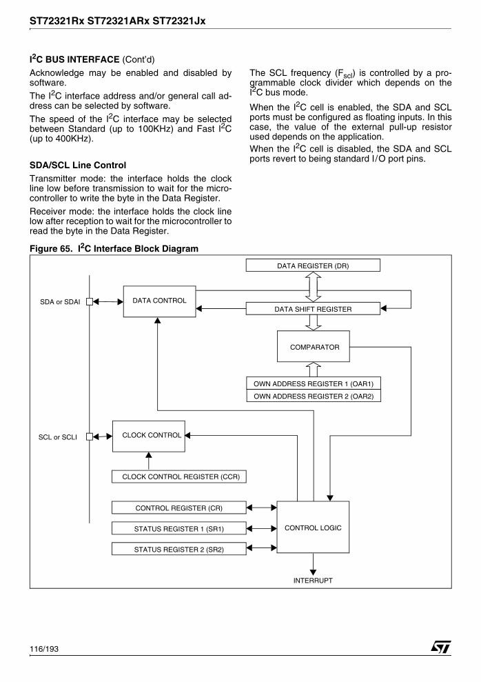
ST72321Rx ST72321ARx ST72321Jx
I2C BUS INTERFACE (Cont’d)
Acknowledge may be enabled and disabled bysoftware.
The I2C interface address and/or general call ad-dress can be selected by software.
The speed of the I2C interface may be selectedbetween Standard (up to 100KHz) and Fast I2C(up to 400KHz).
SDA/SCL Line ControlTransmitter mode: the interface holds the clockline low before transmission to wait for the micro-controller to write the byte in the Data Register.
Receiver mode: the interface holds the clock linelow after reception to wait for the microcontroller toread the byte in the Data Register.
The SCL frequency (Fscl) is controlled by a pro-grammable clock divider which depends on theI2C bus mode.
When the I2C cell is enabled, the SDA and SCLports must be configured as floating inputs. In thiscase, the value of the external pull-up resistorused depends on the application.When the I2C cell is disabled, the SDA and SCLports revert to being standard I/O port pins.
Figure 65. I2C Interface Block Diagram
DATA REGISTER (DR)
DATA SHIFT REGISTER
COMPARATOR
OWN ADDRESS REGISTER 1 (OAR1)
CLOCK CONTROL REGISTER (CCR)
STATUS REGISTER 1 (SR1)
CONTROL REGISTER (CR)
CONTROL LOGIC
STATUS REGISTER 2 (SR2)
INTERRUPT
CLOCK CONTROL
DATA CONTROL
SCL or SCLI
SDA or SDAI
OWN ADDRESS REGISTER 2 (OAR2)
116/193

ST72321Rx ST72321ARx ST72321Jx
I2C BUS INTERFACE (Cont’d)
10.7.4 Functional DescriptionRefer to the CR, SR1 and SR2 registers in Section10.7.7. for the bit definitions.
By default the I2C interface operates in Slavemode (M/SL bit is cleared) except when it initiatesa transmit or receive sequence.
First the interface frequency must be configuredusing the FRi bits in the OAR2 register.
10.7.4.1 Slave ModeAs soon as a start condition is detected, theaddress is received from the SDA line and sent tothe shift register; then it is compared with theaddress of the interface or the General Calladdress (if selected by software).
Note: In 10-bit addressing mode, the comparisonincludes the header sequence (11110xx0) and thetwo most significant bits of the address.
Header matched (10-bit mode only): the interfacegenerates an acknowledge pulse if the ACK bit isset.
Address not matched: the interface ignores itand waits for another Start condition.
Address matched: the interface generates in se-quence:
– Acknowledge pulse if the ACK bit is set.
– EVF and ADSL bits are set with an interrupt if the ITE bit is set.
Then the interface waits for a read of the SR1 reg-ister, holding the SCL line low (see Figure 66Transfer sequencing EV1).Next, in 7-bit mode read the DR register to deter-mine from the least significant bit (Data DirectionBit) if the slave must enter Receiver or Transmittermode.
In 10-bit mode, after receiving the address se-quence the slave is always in receive mode. It willenter transmit mode on receiving a repeated Startcondition followed by the header sequence withmatching address bits and the least significant bitset (11110xx1).
Slave ReceiverFollowing the address reception and after SR1register has been read, the slave receives bytesfrom the SDA line into the DR register via the inter-nal shift register. After each byte the interface gen-erates in sequence:
– Acknowledge pulse if the ACK bit is set
– EVF and BTF bits are set with an interrupt if the ITE bit is set.
Then the interface waits for a read of the SR1 reg-ister followed by a read of the DR register, holdingthe SCL line low (see Figure 66 Transfer se-quencing EV2).
Slave TransmitterFollowing the address reception and after SR1register has been read, the slave sends bytes fromthe DR register to the SDA line via the internal shiftregister.
The slave waits for a read of the SR1 register fol-lowed by a write in the DR register, holding theSCL line low (see Figure 66 Transfer sequencingEV3).
When the acknowledge pulse is received:
– The EVF and BTF bits are set by hardware with an interrupt if the ITE bit is set.
Closing slave communicationAfter the last data byte is transferred a Stop Con-dition is generated by the master. The interfacedetects this condition and sets:
– EVF and STOPF bits with an interrupt if the ITE bit is set.
Then the interface waits for a read of the SR2 reg-ister (see Figure 66 Transfer sequencing EV4).Error Cases
– BERR: Detection of a Stop or a Start condition during a byte transfer. In this case, the EVF and the BERR bits are set with an interrupt if the ITE bit is set. If it is a Stop then the interface discards the data, released the lines and waits for another Start condition.If it is a Start then the interface discards the data and waits for the next slave address on the bus.
– AF: Detection of a non-acknowledge bit. In this case, the EVF and AF bits are set with an inter-rupt if the ITE bit is set.The AF bit is cleared by reading the I2CSR2 reg-ister. However, if read before the completion of the transmission, the AF flag will be set again, thus possibly generating a new interrupt. Soft-ware must ensure either that the SCL line is back at 0 before reading the SR2 register, or be able to correctly handle a second interrupt during the 9th pulse of a transmitted byte.
Note: In case of errors, SCL line is not held low;however, the SDA line can remain low if the lastbits transmitted are all 0. While AF=1, the SCL linemay be held low due to SB or BTF flags that areset at the same time. It is then necessary to re-lease both lines by software.
117/193

ST72321Rx ST72321ARx ST72321Jx
I2C INTERFACE (Cont’d)How to release the SDA / SCL linesSet and subsequently clear the STOP bit whileBTF is set. The SDA/SCL lines are released afterthe transfer of the current byte.
SMBus CompatibilityST7 I2C is compatible with SMBus V1.1 protocol. Itsupports all SMBus adressing modes, SMBus busprotocols and CRC-8 packet error checking. Referto AN1713: SMBus Slave Driver For ST7 I2C Pe-ripheral.
10.7.4.2 Master ModeTo switch from default Slave mode to Mastermode a Start condition generation is needed.
Start condition Setting the START bit while the BUSY bit iscleared causes the interface to switch to Mastermode (M/SL bit set) and generates a Start condi-tion.
Once the Start condition is sent:
– The EVF and SB bits are set by hardware with an interrupt if the ITE bit is set.
Then the master waits for a read of the SR1 regis-ter followed by a write in the DR register with theSlave address, holding the SCL line low (seeFigure 66 Transfer sequencing EV5).
Slave address transmissionThen the slave address is sent to the SDA line viathe internal shift register.
In 7-bit addressing mode, one address byte issent.
In 10-bit addressing mode, sending the first byteincluding the header sequence causes the follow-ing event:– The EVF bit is set by hardware with interrupt
generation if the ITE bit is set. Then the master waits for a read of the SR1 regis-ter followed by a write in the DR register, holdingthe SCL line low (see Figure 66 Transfer se-quencing EV9).
Then the second address byte is sent by the inter-face.
After completion of this transfer (and acknowledgefrom the slave if the ACK bit is set):
– The EVF bit is set by hardware with interrupt generation if the ITE bit is set.
Then the master waits for a read of the SR1 regis-ter followed by a write in the CR register (for exam-ple set PE bit), holding the SCL line low (see Fig-ure 66 Transfer sequencing EV6).
Next the master must enter Receiver or Transmit-ter mode.
Note: In 10-bit addressing mode, to switch themaster to Receiver mode, software must generatea repeated Start condition and resend the headersequence with the least significant bit set(11110xx1).
Master Receiver Following the address transmission and after SR1and CR registers have been accessed, the masterreceives bytes from the SDA line into the DR reg-ister via the internal shift register. After each bytethe interface generates in sequence:
– Acknowledge pulse if the ACK bit is set
– EVF and BTF bits are set by hardware with an in-terrupt if the ITE bit is set.
Then the interface waits for a read of the SR1 reg-ister followed by a read of the DR register, holdingthe SCL line low (see Figure 66 Transfer se-quencing EV7).
To close the communication: before reading thelast byte from the DR register, set the STOP bit togenerate the Stop condition. The interface goesautomatically back to slave mode (M/SL bitcleared).
Note: In order to generate the non-acknowledgepulse after the last received data byte, the ACK bitmust be cleared just before reading the secondlast data byte.
118/193
ST72321Rx ST72321ARx ST72321Jx
I2C BUS INTERFACE (Cont’d)
Master TransmitterFollowing the address transmission and after SR1register has been read, the master sends bytesfrom the DR register to the SDA line via the inter-nal shift register.
The master waits for a read of the SR1 register fol-lowed by a write in the DR register, holding theSCL line low (see Figure 66 Transfer sequencingEV8).
When the acknowledge bit is received, theinterface sets:
– EVF and BTF bits with an interrupt if the ITE bit is set.
To close the communication: after writing the lastbyte to the DR register, set the STOP bit to gener-ate the Stop condition. The interface goes auto-matically back to slave mode (M/SL bit cleared).
Error Cases– BERR: Detection of a Stop or a Start condition
during a byte transfer. In this case, the EVF and BERR bits are set by hardware with an interrupt if ITE is set.Note that BERR will not be set if an error is de-tected during the first or second pulse of each 9-bit transaction:Single Master ModeIf a Start or Stop is issued during the first or sec-ond pulse of a 9-bit transaction, the BERR flag will not be set and transfer will continue however the BUSY flag will be reset. To work around this, slave devices should issue a NACK when they receive a misplaced Start or Stop. The reception of a NACK or BUSY by the master in the middle
of communication gives the possibility to reiniti-ate transmission.Multimaster ModeNormally the BERR bit would be set whenever unauthorized transmission takes place while transfer is already in progress. However, an is-sue will arise if an external master generates an unauthorized Start or Stop while the I2C master is on the first or second pulse of a 9-bit transac-tion. It is possible to work around this by polling the BUSY bit during I2C master mode transmis-sion. The resetting of the BUSY bit can then be handled in a similar manner as the BERR flag being set.
– AF: Detection of a non-acknowledge bit. In this case, the EVF and AF bits are set by hardware with an interrupt if the ITE bit is set. To resume, set the Start or Stop bit.The AF bit is cleared by reading the I2CSR2 reg-ister. However, if read before the completion of the transmission, the AF flag will be set again, thus possibly generating a new interrupt. Soft-ware must ensure either that the SCL line is back at 0 before reading the SR2 register, or be able to correctly handle a second interrupt during the 9th pulse of a transmitted byte.
– ARLO: Detection of an arbitration lost condition.In this case the ARLO bit is set by hardware (with an interrupt if the ITE bit is set and the interface goes automatically back to slave mode (the M/SL bit is cleared).
Note: In all these cases, the SCL line is not heldlow; however, the SDA line can remain low due topossible «0» bits transmitted last. It is then neces-sary to release both lines by software.
119/193

ST72321Rx ST72321ARx ST72321Jx
I2C BUS INTERFACE (Cont’d)
Figure 66. Transfer Sequencing
Legend: S=Start, Sr = Repeated Start, P=Stop, A=Acknowledge, NA=Non-acknowledge,EVx=Event (with interrupt if ITE=1)EV1: EVF=1, ADSL=1, cleared by reading SR1 register.EV2: EVF=1, BTF=1, cleared by reading SR1 register followed by reading DR register.EV3: EVF=1, BTF=1, cleared by reading SR1 register followed by writing DR register.EV3-1: EVF=1, AF=1, BTF=1; AF is cleared by reading SR1 register. BTF is cleared by releasing thelines (STOP=1, STOP=0) or by writing DR register (DR=FFh). Note: If lines are released bySTOP=1, STOP=0, the subsequent EV4 is not seen.EV4: EVF=1, STOPF=1, cleared by reading SR2 register.EV5: EVF=1, SB=1, cleared by reading SR1 register followed by writing DR register.EV6: EVF=1, cleared by reading SR1 register followed by writing CR register (for example PE=1).EV7: EVF=1, BTF=1, cleared by reading SR1 register followed by reading DR register.EV8: EVF=1, BTF=1, cleared by reading SR1 register followed by writing DR register.EV9: EVF=1, ADD10=1, cleared by reading SR1 register followed by writing DR register.
7-bit Slave receiver:
7-bit Slave transmitter:
7-bit Master receiver:
7-bit Master transmitter:
10-bit Slave receiver:
10-bit Slave transmitter:
10-bit Master transmitter
10-bit Master receiver:
S Address A Data1 A Data2 A.....
DataN A P
EV1 EV2 EV2 EV2 EV4
S Address A Data1 A Data2 A.....
DataN NA P
EV1 EV3 EV3 EV3 EV3-1 EV4
S Address A Data1 A Data2 A.....
DataN NA P
EV5 EV6 EV7 EV7 EV7
S Address A Data1 A Data2 A.....
DataN A P
EV5 EV6 EV8 EV8 EV8 EV8
S Header A Address A Data1 A.....
DataN A P
EV1 EV2 EV2 EV4
Sr Header A Data1 A .....
DataN A P
EV1 EV3 EV3 EV3-1 EV4
S Header A Address A Data1 A.....
DataN A P
EV5 EV9 EV6 EV8 EV8 EV8
Sr Header A Data1 A.....
DataN A P
EV5 EV6 EV7 EV7
120/193

ST72321Rx ST72321ARx ST72321Jx
I2C BUS INTERFACE (Cont’d)
10.7.5 Low Power Modes
10.7.6 Interrupts
Figure 67. Event Flags and Interrupt Generation
Note: The I2C interrupt events are connected tothe same interrupt vector (see Interrupts chapter). They generate an interrupt if the correspondingEnable Control Bit is set and the I-bit in the CC reg-ister is reset (RIM instruction).
Mode Description
WAITNo effect on I2C interface. I2C interrupts cause the device to exit from WAIT mode.
HALTI2C registers are frozen.In HALT mode, the I2C interface is inactive and does not acknowledge data on the bus. The I2C interface resumes operation when the MCU is woken up by an interrupt with “exit from HALT mode” capability.
Interrupt EventEventFlag
Enable Control
Bit
Exit fromWait
Exit from Halt
10-bit Address Sent Event (Master mode) ADD10
ITE
Yes NoEnd of Byte Transfer Event BTF Yes NoAddress Matched Event (Slave mode) ADSEL Yes NoStart Bit Generation Event (Master mode) SB Yes NoAcknowledge Failure Event AF Yes NoStop Detection Event (Slave mode) STOPF Yes NoArbitration Lost Event (Multimaster configuration) ARLO Yes NoBus Error Event BERR Yes No
BTFADSL
SBAF
STOPFARLOBERR
EVF
INTERRUPT
ITE
** EVF can also be set by EV6 or an error from the SR2 register.
ADD10
121/193

ST72321Rx ST72321ARx ST72321Jx
I2C BUS INTERFACE (Cont’d)
10.7.7 Register DescriptionI2C CONTROL REGISTER (CR)Read / WriteReset Value: 0000 0000 (00h)
Bit 7:6 = Reserved. Forced to 0 by hardware.
Bit 5 = PE Peripheral enable. This bit is set and cleared by software.0: Peripheral disabled 1: Master/Slave capabilityNotes:– When PE=0, all the bits of the CR register and
the SR register except the Stop bit are reset. All outputs are released while PE=0
– When PE=1, the corresponding I/O pins are se-lected by hardware as alternate functions.
– To enable the I2C interface, write the CR register TWICE with PE=1 as the first write only activates the interface (only PE is set).
Bit 4 = ENGC Enable General Call. This bit is set and cleared by software. It is also cleared by hardware when the interface is disa-bled (PE=0). The 00h General Call address is ac-knowledged (01h ignored).0: General Call disabled 1: General Call enabled
Note: In accordance with the I2C standard, when GCAL addressing is enabled, an I2C slave can only receive data. It will not transmit data to the master.
Bit 3 = START Generation of a Start condition.This bit is set and cleared by software. It is alsocleared by hardware when the interface is disa-bled (PE=0) or when the Start condition is sent(with interrupt generation if ITE=1).
– In master mode:0: No start generation1: Repeated start generation
– In slave mode:0: No start generation 1: Start generation when the bus is free
Bit 2 = ACK Acknowledge enable. This bit is set and cleared by software. It is alsocleared by hardware when the interface is disa-bled (PE=0).0: No acknowledge returned 1: Acknowledge returned after an address byte or
a data byte is received
Bit 1 = STOP Generation of a Stop condition. This bit is set and cleared by software. It is alsocleared by hardware in master mode. Note: Thisbit is not cleared when the interface is disabled(PE=0).
– In master mode:0: No stop generation1: Stop generation after the current byte transfer or after the current Start condition is sent. The STOP bit is cleared by hardware when the Stop condition is sent.
– In slave mode:0: No stop generation 1: Release the SCL and SDA lines after the cur-rent byte transfer (BTF=1). In this mode the STOP bit has to be cleared by software.
Bit 0 = ITE Interrupt enable. This bit is set and cleared by software and cleared by hardware when the interface is disabled (PE=0).0: Interrupts disabled 1: Interrupts enabledRefer to Figure 67 for the relationship between the events and the interrupt.SCL is held low when the ADD10, SB, BTF or ADSL flags or an EV6 event (See Figure 66) is de-tected.
7 0
0 0 PE ENGC START ACK STOP ITE
122/193

ST72321Rx ST72321ARx ST72321Jx
I2C BUS INTERFACE (Cont’d)
I2C STATUS REGISTER 1 (SR1) Read Only
Reset Value: 0000 0000 (00h)
Bit 7 = EVF Event flag. This bit is set by hardware as soon as an event oc-curs. It is cleared by software reading SR2 registerin case of error event or as described in Figure 66.It is also cleared by hardware when the interface isdisabled (PE=0).0: No event1: One of the following events has occurred:
– BTF=1 (Byte received or transmitted)
– ADSL=1 (Address matched in Slave modewhile ACK=1)
– SB=1 (Start condition generated in Mastermode)
– AF=1 (No acknowledge received after bytetransmission)
– STOPF=1 (Stop condition detected in Slavemode)
– ARLO=1 (Arbitration lost in Master mode)
– BERR=1 (Bus error, misplaced Start or Stopcondition detected)
– ADD10=1 (Master has sent header byte)
– Address byte successfully transmitted in Mas-ter mode.
Bit 6 = ADD10 10-bit addressing in Master mode.This bit is set by hardware when the master hassent the first byte in 10-bit address mode. It iscleared by software reading SR2 register followedby a write in the DR register of the second addressbyte. It is also cleared by hardware when the pe-ripheral is disabled (PE=0).
0: No ADD10 event occurred.1: Master has sent first address byte (header)
Bit 5 = TRA Transmitter/Receiver.When BTF is set, TRA=1 if a data byte has beentransmitted. It is cleared automatically when BTFis cleared. It is also cleared by hardware after de-tection of Stop condition (STOPF=1), loss of busarbitration (ARLO=1) or when the interface is disa-bled (PE=0).0: Data byte received (if BTF=1)
1: Data byte transmitted
Bit 4 = BUSY Bus busy. This bit is set by hardware on detection of a Startcondition and cleared by hardware on detection ofa Stop condition. It indicates a communication inprogress on the bus. The BUSY flag of the I2CSR1register is cleared if a Bus Error occurs.0: No communication on the bus1: Communication ongoing on the busNote:– The BUSY flag is NOT updated when the inter-
face is disabled (PE=0). This can have conse-quences when operating in Multimaster mode; i.e. a second active I2C master commencing a transfer with an unset BUSY bit can cause a con-flict resulting in lost data. A software workaround consists of checking that the I2C is not busy be-fore enabling the I2C Multimaster cell.
Bit 3 = BTF Byte transfer finished. This bit is set by hardware as soon as a byte is cor-rectly received or transmitted with interrupt gener-ation if ITE=1. It is cleared by software readingSR1 register followed by a read or write of DR reg-ister. It is also cleared by hardware when the inter-face is disabled (PE=0).
– Following a byte transmission, this bit is set after reception of the acknowledge clock pulse. In case an address byte is sent, this bit is set only after the EV6 event (See Figure 66). BTF is cleared by reading SR1 register followed by writ-ing the next byte in DR register.
– Following a byte reception, this bit is set after transmission of the acknowledge clock pulse if ACK=1. BTF is cleared by reading SR1 register followed by reading the byte from DR register.
The SCL line is held low while BTF=1.
0: Byte transfer not done1: Byte transfer succeeded
Bit 2 = ADSL Address matched (Slave mode).This bit is set by hardware as soon as the receivedslave address matched with the OAR register con-tent or a general call is recognized. An interrupt isgenerated if ITE=1. It is cleared by software read-ing SR1 register or by hardware when the inter-face is disabled (PE=0).
The SCL line is held low while ADSL=1.
0: Address mismatched or not received1: Received address matched
7 0
EVF ADD10 TRA BUSY BTF ADSL M/SL SB
123/193

ST72321Rx ST72321ARx ST72321Jx
I2C BUS INTERFACE (Cont’d)
Bit 1 = M/SL Master/Slave.This bit is set by hardware as soon as the interfaceis in Master mode (writing START=1). It is clearedby hardware after detecting a Stop condition onthe bus or a loss of arbitration (ARLO=1). It is alsocleared when the interface is disabled (PE=0).0: Slave mode1: Master mode
Bit 0 = SB Start bit (Master mode).This bit is set by hardware as soon as the Startcondition is generated (following a writeSTART=1). An interrupt is generated if ITE=1. It iscleared by software reading SR1 register followedby writing the address byte in DR register. It is alsocleared by hardware when the interface is disa-bled (PE=0).0: No Start condition1: Start condition generated
I2C STATUS REGISTER 2 (SR2)Read Only Reset Value: 0000 0000 (00h)
Bit 7:5 = Reserved. Forced to 0 by hardware.
Bit 4 = AF Acknowledge failure. This bit is set by hardware when no acknowledgeis returned. An interrupt is generated if ITE=1. It iscleared by software reading SR2 register or byhardware when the interface is disabled (PE=0).
The SCL line is not held low while AF=1 but by oth-er flags (SB or BTF) that are set at the same time.
0: No acknowledge failure1: Acknowledge failureNote: – When an AF event occurs, the SCL line is not
held low; however, the SDA line can remain low if the last bits transmitted are all 0. It is then nec-essary to release both lines by software.
Bit 3 = STOPF Stop detection (Slave mode). This bit is set by hardware when a Stop conditionis detected on the bus after an acknowledge (ifACK=1). An interrupt is generated if ITE=1. It iscleared by software reading SR2 register or byhardware when the interface is disabled (PE=0).
The SCL line is not held low while STOPF=1.
0: No Stop condition detected1: Stop condition detected
Bit 2 = ARLO Arbitration lost.This bit is set by hardware when the interface los-es the arbitration of the bus to another master. Aninterrupt is generated if ITE=1. It is cleared by soft-ware reading SR2 register or by hardware whenthe interface is disabled (PE=0).
After an ARLO event the interface switches backautomatically to Slave mode (M/SL=0).
The SCL line is not held low while ARLO=1.
0: No arbitration lost detected1: Arbitration lost detectedNote:– In a Multimaster environment, when the interface
is configured in Master Receive mode it does not perform arbitration during the reception of the Acknowledge Bit. Mishandling of the ARLO bit from the I2CSR2 register may occur when a sec-ond master simultaneously requests the same data from the same slave and the I2C master does not acknowledge the data. The ARLO bit is then left at 0 instead of being set.
Bit 1 = BERR Bus error.This bit is set by hardware when the interface de-tects a misplaced Start or Stop condition. An inter-rupt is generated if ITE=1. It is cleared by softwarereading SR2 register or by hardware when the in-terface is disabled (PE=0).
The SCL line is not held low while BERR=1.
0: No misplaced Start or Stop condition1: Misplaced Start or Stop conditionNote:– If a Bus Error occurs, a Stop or a repeated Start
condition should be generated by the Master to re-synchronize communication, get the transmis-sion acknowledged and the bus released for fur-ther communication
Bit 0 = GCAL General Call (Slave mode). This bit is set by hardware when a general call ad-dress is detected on the bus while ENGC=1. It iscleared by hardware detecting a Stop condition(STOPF=1) or when the interface is disabled(PE=0).
0: No general call address detected on bus1: general call address detected on bus
7 0
0 0 0 AF STOPF ARLO BERR GCAL
124/193

ST72321Rx ST72321ARx ST72321Jx
I2C BUS INTERFACE (Cont’d)
I2C CLOCK CONTROL REGISTER (CCR) Read / WriteReset Value: 0000 0000 (00h)
Bit 7 = FM/SM Fast/Standard I2C mode. This bit is set and cleared by software. It is notcleared when the interface is disabled (PE=0).0: Standard I2C mode1: Fast I2C mode
Bit 6:0 = CC[6:0] 7-bit clock divider. These bits select the speed of the bus (FSCL) de-pending on the I2C mode. They are not clearedwhen the interface is disabled (PE=0).
Refer to the Electrical Characteristics section forthe table of values.
Note: The programmed FSCL assumes no load onSCL and SDA lines.
I2C DATA REGISTER (DR) Read / WriteReset Value: 0000 0000 (00h)
Bit 7:0 = D[7:0] 8-bit Data Register. These bits contain the byte to be received or trans-mitted on the bus.
– Transmitter mode: Byte transmission start auto-matically when the software writes in the DR reg-ister.
– Receiver mode: the first data byte is received au-tomatically in the DR register using the least sig-nificant bit of the address.Then, the following data bytes are received one by one after reading the DR register.
7 0
FM/SM CC6 CC5 CC4 CC3 CC2 CC1 CC0
7 0
D7 D6 D5 D4 D3 D2 D1 D0
125/193

ST72321Rx ST72321ARx ST72321Jx
I2C BUS INTERFACE (Cont’d)
I2C OWN ADDRESS REGISTER (OAR1) Read / WriteReset Value: 0000 0000 (00h)
7-bit Addressing ModeBit 7:1 = ADD[7:1] Interface address. These bits define the I2C bus address of the inter-face. They are not cleared when the interface isdisabled (PE=0).
Bit 0 = ADD0 Address direction bit. This bit is don’t care, the interface acknowledgeseither 0 or 1. It is not cleared when the interface isdisabled (PE=0).
Note: Address 01h is always ignored.
10-bit Addressing ModeBit 7:0 = ADD[7:0] Interface address. These are the least significant bits of the I2C busaddress of the interface. They are not clearedwhen the interface is disabled (PE=0).
I2C OWN ADDRESS REGISTER (OAR2) Read / WriteReset Value: 0100 0000 (40h)
Bit 7:6 = FR[1:0] Frequency bits.
These bits are set by software only when the inter-face is disabled (PE=0). To configure the interfaceto I2C specified delays select the value corre-sponding to the microcontroller frequency FCPU.
Bit 5:3 = Reserved
Bit 2:1 = ADD[9:8] Interface address. These are the most significant bits of the I2C busaddress of the interface (10-bit mode only). Theyare not cleared when the interface is disabled(PE=0).
Bit 0 = Reserved.
7 0
ADD7 ADD6 ADD5 ADD4 ADD3 ADD2 ADD1 ADD0
7 0
FR1 FR0 0 0 0 ADD9 ADD8 0
fCPU FR1 FR0< 6 MHz 0 0
6 to 8 MHz 0 1
126/193

ST72321Rx ST72321ARx ST72321Jx
I²C BUS INTERFACE (Cont’d)
Table 24. I2C Register Map and Reset Values
Address
(Hex.)Register
Label7 6 5 4 3 2 1 0
0018hI2CCRReset Value 0 0
PE0
ENGC0
START0
ACK0
STOP0
ITE0
0019hI2CSR1Reset Value
EVF0
ADD100
TRA0
BUSY0
BTF0
ADSL0
M/SL0
SB0
001AhI2CSR2Reset Value 0 0 0
AF0
STOPF0
ARLO0
BERR0
GCAL0
001BhI2CCCRReset Value
FM/SM0
CC60
CC50
CC40
CC30
CC20
CC10
CC00
001ChI2COAR1Reset Value
ADD70
ADD60
ADD50
ADD40
ADD30
ADD20
ADD10
ADD00
001DhI2COAR2Reset Value
FR10
FR01 0 0 0
ADD90
ADD80 0
001EhI2CDRReset Value
MSB0 0 0 0 0 0 0
LSB0
127/193

ST72321Rx ST72321ARx ST72321Jx
10.8 10-BIT A/D CONVERTER (ADC)
10.8.1 IntroductionThe on-chip Analog to Digital Converter (ADC) pe-ripheral is a 10-bit, successive approximation con-verter with internal sample and hold circuitry. Thisperipheral has up to 16 multiplexed analog inputchannels (refer to device pin out description) thatallow the peripheral to convert the analog voltagelevels from up to 16 different sources.
The result of the conversion is stored in a 10-bitData Register. The A/D converter is controlledthrough a Control/Status Register.
10.8.2 Main Features■ 10-bit conversion■ Up to 16 channels with multiplexed input■ Linear successive approximation■ Data register (DR) which contains the results■ Conversion complete status flag■ On/off bit (to reduce consumption)
The block diagram is shown in Figure 68.
Figure 68. ADC Block Diagram
CH2 CH1EOC SPEED ADON 0 CH0 ADCCSR
AIN0
AIN1 ANALOG TO DIGITAL
CONVERTER
AINx
ANALOGMUX
D4 D3D5D9 D8 D7 D6 D2ADCDRH
4
DIV 4fADC
fCPU
D1 D0ADCDRL
0
1
0 0 0 0 0 0
CH3
DIV 2
128/193

ST72321Rx ST72321ARx ST72321Jx
10-BIT A/D CONVERTER (ADC) (Cont’d)
10.8.3 Functional DescriptionThe conversion is monotonic, meaning that the re-sult never decreases if the analog input does notand never increases if the analog input does not.
If the input voltage (VAIN) is greater than VAREF(high-level voltage reference) then the conversionresult is FFh in the ADCDRH register and 03h inthe ADCDRL register (without overflow indication).
If the input voltage (VAIN) is lower than VSSA (low-level voltage reference) then the conversion resultin the ADCDRH and ADCDRL registers is 00 00h.
The A/D converter is linear and the digital result ofthe conversion is stored in the ADCDRH and AD-CDRL registers. The accuracy of the conversion isdescribed in the Electrical Characteristics Section.
RAIN is the maximum recommended impedancefor an analog input signal. If the impedance is toohigh, this will result in a loss of accuracy due toleakage and sampling not being completed in thealloted time.
10.8.3.1 A/D Converter Configuration The analog input ports must be configured as in-put, no pull-up, no interrupt. Refer to the «I/Oports» chapter. Using these pins as analog inputsdoes not affect the ability of the port to be read asa logic input.
In the ADCCSR register:
– Select the CS[3:0] bits to assign the analogchannel to convert.
10.8.3.2 Starting the ConversionIn the ADCCSR register:
– Set the ADON bit to enable the A/D converter and to start the conversion. From this time on, the ADC performs a continuous conversion of the selected channel.
When a conversion is complete:
– The EOC bit is set by hardware.– The result is in the ADCDR registers.
A read to the ADCDRH or a write to any bit of theADCCSR register resets the EOC bit.
To read the 10 bits, perform the following steps:
1. Poll the EOC bit
2. Read the ADCDRL register
3. Read the ADCDRH register. This clears EOCautomatically.
Note: The data is not latched, so both the low andthe high data register must be read before the nextconversion is complete, so it is recommended todisable interrupts while reading the conversion re-sult.
To read only 8 bits, perform the following steps:
1. Poll the EOC bit
2. Read the ADCDRH register. This clears EOCautomatically.
10.8.3.3 Changing the conversion channelThe application can change channels during con-version. When software modifies the CH[3:0] bitsin the ADCCSR register, the current conversion isstopped, the EOC bit is cleared, and the A/D con-verter starts converting the newly selected chan-nel.
10.8.4 Low Power ModesNote: The A/D converter may be disabled by re-setting the ADON bit. This feature allows reducedpower consumption when no conversion is need-ed and between single shot conversions.
10.8.5 InterruptsNone.
Mode Description WAIT No effect on A/D Converter
HALT
A/D Converter disabled.
After wakeup from Halt mode, the A/D Converter requires a stabilization time tSTAB (see Electrical Characteristics) before accurate conversions can be performed.
129/193

ST72321Rx ST72321ARx ST72321Jx
10-BIT A/D CONVERTER (ADC) (Cont’d)
10.8.6 Register Description
CONTROL/STATUS REGISTER (ADCCSR)Read/Write (Except bit 7 read only)
Reset Value: 0000 0000 (00h)
Bit 7 = EOC End of ConversionThis bit is set by hardware. It is cleared by hard-ware when software reads the ADCDRH registeror writes to any bit of the ADCCSR register.0: Conversion is not complete1: Conversion complete
Bit 6 = SPEED ADC clock selectionThis bit is set and cleared by software.0: fADC = fCPU/41: fADC = fCPU/2
Bit 5 = ADON A/D Converter onThis bit is set and cleared by software.0: Disable ADC and stop conversion1: Enable ADC and start conversion
Bit 4 = Reserved. Must be kept cleared.
Bit 3:0 = CH[3:0] Channel SelectionThese bits are set and cleared by software. Theyselect the analog input to convert.
*The number of channels is device dependent. Refer tothe device pinout description.
DATA REGISTER (ADCDRH)Read Only
Reset Value: 0000 0000 (00h)
Bit 7:0 = D[9:2] MSB of Converted Analog Value
DATA REGISTER (ADCDRL)Read Only
Reset Value: 0000 0000 (00h)
Bit 7:2 = Reserved. Forced by hardware to 0.
Bit 1:0 = D[1:0] LSB of Converted Analog Value
7 0
EOC SPEED ADON 0 CH3 CH2 CH1 CH0
Channel Pin* CH3 CH2 CH1 CH0
AIN0 0 0 0 0AIN1 0 0 0 1AIN2 0 0 1 0AIN3 0 0 1 1AIN4 0 1 0 0AIN5 0 1 0 1AIN6 0 1 1 0AIN7 0 1 1 1AIN8 1 0 0 0AIN9 1 0 0 1AIN10 1 0 1 0AIN11 1 0 1 1AIN12 1 1 0 0AIN13 1 1 0 1AIN14 1 1 1 0AIN15 1 1 1 1
7 0
D9 D8 D7 D6 D5 D4 D3 D2
7 0
0 0 0 0 0 0 D1 D0
130/193

ST72321Rx ST72321ARx ST72321Jx
10-BIT A/D CONVERTER (Cont’d)
Table 25. ADC Register Map and Reset Values
Address(Hex.)
RegisterLabel
7 6 5 4 3 2 1 0
0070hADCCSRReset Value
EOC0
SPEED0
ADON0 0
CH30
CH20
CH10
CH00
0071hADCDRHReset Value
D90
D80
D70
D60
D50
D40
D30
D20
0072hADCDRLReset Value 0 0 0 0 0 0
D10
D00
131/193

ST72321Rx ST72321ARx ST72321Jx
11 INSTRUCTION SET
11.1 CPU ADDRESSING MODES
The CPU features 17 different addressing modeswhich can be classified in seven main groups:
The CPU Instruction set is designed to minimizethe number of bytes required per instruction: To do
so, most of the addressing modes may be subdi-vided in two submodes called long and short:
– Long addressing mode is more powerful be-cause it can use the full 64 Kbyte address space, however it uses more bytes and more CPU cy-cles.
– Short addressing mode is less powerful because it can generally only access page zero (0000h - 00FFh range), but the instruction size is more compact, and faster. All memory to memory in-structions use short addressing modes only (CLR, CPL, NEG, BSET, BRES, BTJT, BTJF, INC, DEC, RLC, RRC, SLL, SRL, SRA, SWAP)
The ST7 Assembler optimizes the use of long andshort addressing modes.
Table 26. CPU Addressing Mode Overview
Addressing Mode Example
Inherent nop
Immediate ld A,#$55
Direct ld A,$55
Indexed ld A,($55,X)
Indirect ld A,([$55],X)
Relative jrne loop
Bit operation bset byte,#5
Mode Syntax DestinationPointer Address
(Hex.)
Pointer Size(Hex.)
Length(Bytes)
Inherent nop + 0
Immediate ld A,#$55 + 1
Short Direct ld A,$10 00..FF + 1
Long Direct ld A,$1000 0000..FFFF + 2
No Offset Direct Indexed ld A,(X) 00..FF + 0
Short Direct Indexed ld A,($10,X) 00..1FE + 1
Long Direct Indexed ld A,($1000,X) 0000..FFFF + 2
Short Indirect ld A,[$10] 00..FF 00..FF byte + 2
Long Indirect ld A,[$10.w] 0000..FFFF 00..FF word + 2
Short Indirect Indexed ld A,([$10],X) 00..1FE 00..FF byte + 2
Long Indirect Indexed ld A,([$10.w],X) 0000..FFFF 00..FF word + 2
Relative Direct jrne loop PC+/-127 + 1
Relative Indirect jrne [$10] PC+/-127 00..FF byte + 2
Bit Direct bset $10,#7 00..FF + 1
Bit Indirect bset [$10],#7 00..FF 00..FF byte + 2
Bit Direct Relative btjt $10,#7,skip 00..FF + 2
Bit Indirect Relative btjt [$10],#7,skip 00..FF 00..FF byte + 3
132/193

ST72321Rx ST72321ARx ST72321Jx
INSTRUCTION SET OVERVIEW (Cont’d)
11.1.1 InherentAll Inherent instructions consist of a single byte.The opcode fully specifies all the required informa-tion for the CPU to process the operation.
11.1.2 ImmediateImmediate instructions have 2 bytes, the first bytecontains the opcode, the second byte contains theoperand value.
11.1.3 DirectIn Direct instructions, the operands are referencedby their memory address.
The direct addressing mode consists of two sub-modes:
Direct (short)The address is a byte, thus requires only one byteafter the opcode, but only allows 00 - FF address-ing space.
Direct (long)The address is a word, thus allowing 64 Kbyte ad-dressing space, but requires 2 bytes after the op-code.
11.1.4 Indexed (No Offset, Short, Long)In this mode, the operand is referenced by itsmemory address, which is defined by the unsignedaddition of an index register (X or Y) with an offset.
The indirect addressing mode consists of threesubmodes:
Indexed (No Offset)There is no offset, (no extra byte after the opcode),and allows 00 - FF addressing space.
Indexed (Short)The offset is a byte, thus requires only one byte af-ter the opcode and allows 00 - 1FE addressingspace.
Indexed (long)The offset is a word, thus allowing 64 Kbyte ad-dressing space and requires 2 bytes after the op-code.
11.1.5 Indirect (Short, Long)The required data byte to do the operation is foundby its memory address, located in memory (point-er).
The pointer address follows the opcode. The indi-rect addressing mode consists of two submodes:
Indirect (short)The pointer address is a byte, the pointer size is abyte, thus allowing 00 - FF addressing space, andrequires 1 byte after the opcode.
Indirect (long)The pointer address is a byte, the pointer size is aword, thus allowing 64 Kbyte addressing space,and requires 1 byte after the opcode.
Inherent Instruction Function
NOP No operation
TRAP S/W Interrupt
WFIWait For Interrupt (Low Pow-er Mode)
HALTHalt Oscillator (Lowest Power Mode)
RET Sub-routine Return
IRET Interrupt Sub-routine Return
SIM Set Interrupt Mask (level 3)
RIM Reset Interrupt Mask (level 0)
SCF Set Carry Flag
RCF Reset Carry Flag
RSP Reset Stack Pointer
LD Load
CLR Clear
PUSH/POP Push/Pop to/from the stack
INC/DEC Increment/Decrement
TNZ Test Negative or Zero
CPL, NEG 1 or 2 Complement
MUL Byte Multiplication
SLL, SRL, SRA, RLC, RRC
Shift and Rotate Operations
SWAP Swap Nibbles
Immediate Instruction Function
LD Load
CP Compare
BCP Bit Compare
AND, OR, XOR Logical Operations
ADC, ADD, SUB, SBC Arithmetic Operations
133/193

ST72321Rx ST72321ARx ST72321Jx
INSTRUCTION SET OVERVIEW (Cont’d)
11.1.6 Indirect Indexed (Short, Long)This is a combination of indirect and short indexedaddressing modes. The operand is referenced byits memory address, which is defined by the un-signed addition of an index register value (X or Y)with a pointer value located in memory. The point-er address follows the opcode.
The indirect indexed addressing mode consists oftwo submodes:
Indirect Indexed (Short)The pointer address is a byte, the pointer size is abyte, thus allowing 00 - 1FE addressing space,and requires 1 byte after the opcode.
Indirect Indexed (Long)The pointer address is a byte, the pointer size is aword, thus allowing 64 Kbyte addressing space,and requires 1 byte after the opcode.
Table 27. Instructions Supporting Direct,Indexed, Indirect and Indirect IndexedAddressing Modes
11.1.7 Relative mode (Direct, Indirect)This addressing mode is used to modify the PCregister value, by adding an 8-bit signed offset toit.
The relative addressing mode consists of two sub-modes:
Relative (Direct)The offset is following the opcode.
Relative (Indirect)The offset is defined in memory, which addressfollows the opcode.
Long and Short Instructions
Function
LD Load
CP Compare
AND, OR, XOR Logical Operations
ADC, ADD, SUB, SBCArithmetic Additions/Sub-stractions operations
BCP Bit Compare
Short Instructions Only Function
CLR Clear
INC, DEC Increment/Decrement
TNZ Test Negative or Zero
CPL, NEG 1 or 2 Complement
BSET, BRES Bit Operations
BTJT, BTJFBit Test and Jump Opera-tions
SLL, SRL, SRA, RLC, RRC
Shift and Rotate Operations
SWAP Swap Nibbles
CALL, JP Call or Jump subroutine
Available Relative Direct/Indirect Instructions
Function
JRxx Conditional Jump
CALLR Call Relative
134/193

ST72321Rx ST72321ARx ST72321Jx
INSTRUCTION SET OVERVIEW (Cont’d)
11.2 INSTRUCTION GROUPS
The ST7 family devices use an Instruction Setconsisting of 63 instructions. The instructions may
be subdivided into 13 main groups as illustrated inthe following table:
Using a prebyteThe instructions are described with one to four op-codes.
In order to extend the number of available op-codes for an 8-bit CPU (256 opcodes), three differ-ent prebyte opcodes are defined. These prebytesmodify the meaning of the instruction they pre-cede.
The whole instruction becomes:
PC-2 End of previous instruction
PC-1 Prebyte
PC Opcode
PC+1 Additional word (0 to 2) accordingto the number of bytes required to compute the ef-fective address
These prebytes enable instruction in Y as well asindirect addressing modes to be implemented.They precede the opcode of the instruction in X orthe instruction using direct addressing mode. Theprebytes are:
PDY 90 Replace an X based instructionusing immediate, direct, indexed, or inherent ad-dressing mode by a Y one.
PIX 92 Replace an instruction using di-rect, direct bit, or direct relative addressing modeto an instruction using the corresponding indirectaddressing mode.It also changes an instruction using X indexed ad-dressing mode to an instruction using indirect X in-dexed addressing mode.
PIY 91 Replace an instruction using X in-direct indexed addressing mode by a Y one.
Load and Transfer LD CLR
Stack operation PUSH POP RSP
Increment/Decrement INC DEC
Compare and Tests CP TNZ BCP
Logical operations AND OR XOR CPL NEG
Bit Operation BSET BRES
Conditional Bit Test and Branch BTJT BTJF
Arithmetic operations ADC ADD SUB SBC MUL
Shift and Rotates SLL SRL SRA RLC RRC SWAP SLA
Unconditional Jump or Call JRA JRT JRF JP CALL CALLR NOP RET
Conditional Branch JRxx
Interruption management TRAP WFI HALT IRET
Condition Code Flag modification SIM RIM SCF RCF
135/193
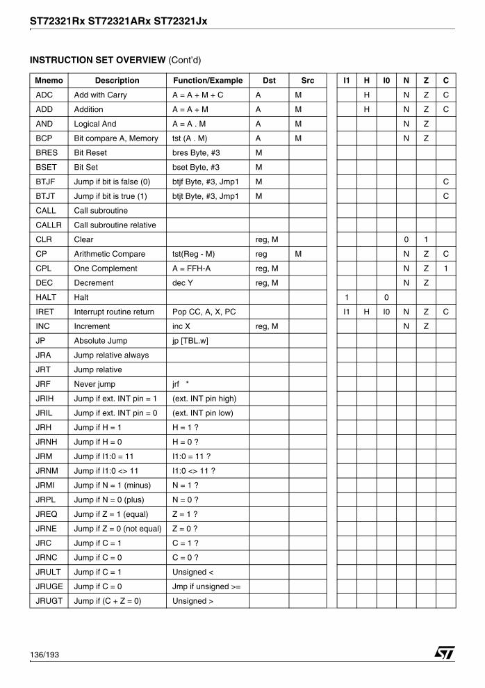
ST72321Rx ST72321ARx ST72321Jx
INSTRUCTION SET OVERVIEW (Cont’d)
Mnemo Description Function/Example Dst Src I1 H I0 N Z C
ADC Add with Carry A = A + M + C A M H N Z C
ADD Addition A = A + M A M H N Z C
AND Logical And A = A . M A M N Z
BCP Bit compare A, Memory tst (A . M) A M N Z
BRES Bit Reset bres Byte, #3 M
BSET Bit Set bset Byte, #3 M
BTJF Jump if bit is false (0) btjf Byte, #3, Jmp1 M C
BTJT Jump if bit is true (1) btjt Byte, #3, Jmp1 M C
CALL Call subroutine
CALLR Call subroutine relative
CLR Clear reg, M 0 1
CP Arithmetic Compare tst(Reg - M) reg M N Z C
CPL One Complement A = FFH-A reg, M N Z 1
DEC Decrement dec Y reg, M N Z
HALT Halt 1 0
IRET Interrupt routine return Pop CC, A, X, PC I1 H I0 N Z C
INC Increment inc X reg, M N Z
JP Absolute Jump jp [TBL.w]
JRA Jump relative always
JRT Jump relative
JRF Never jump jrf *
JRIH Jump if ext. INT pin = 1 (ext. INT pin high)
JRIL Jump if ext. INT pin = 0 (ext. INT pin low)
JRH Jump if H = 1 H = 1 ?
JRNH Jump if H = 0 H = 0 ?
JRM Jump if I1:0 = 11 I1:0 = 11 ?
JRNM Jump if I1:0 <> 11 I1:0 <> 11 ?
JRMI Jump if N = 1 (minus) N = 1 ?
JRPL Jump if N = 0 (plus) N = 0 ?
JREQ Jump if Z = 1 (equal) Z = 1 ?
JRNE Jump if Z = 0 (not equal) Z = 0 ?
JRC Jump if C = 1 C = 1 ?
JRNC Jump if C = 0 C = 0 ?
JRULT Jump if C = 1 Unsigned <
JRUGE Jump if C = 0 Jmp if unsigned >=
JRUGT Jump if (C + Z = 0) Unsigned >
136/193

ST72321Rx ST72321ARx ST72321Jx
INSTRUCTION SET OVERVIEW (Cont’d)
Mnemo Description Function/Example Dst Src I1 H I0 N Z C
JRULE Jump if (C + Z = 1) Unsigned <=
LD Load dst <= src reg, M M, reg N Z
MUL Multiply X,A = X * A A, X, Y X, Y, A 0 0
NEG Negate (2's compl) neg $10 reg, M N Z C
NOP No Operation
OR OR operation A = A + M A M N Z
POP Pop from the Stackpop reg reg M
pop CC CC M I1 H I0 N Z C
PUSH Push onto the Stack push Y M reg, CC
RCF Reset carry flag C = 0 0
RET Subroutine Return
RIM Enable Interrupts I1:0 = 10 (level 0) 1 0
RLC Rotate left true C C <= A <= C reg, M N Z C
RRC Rotate right true C C => A => C reg, M N Z C
RSP Reset Stack Pointer S = Max allowed
SBC Substract with Carry A = A - M - C A M N Z C
SCF Set carry flag C = 1 1
SIM Disable Interrupts I1:0 = 11 (level 3) 1 1
SLA Shift left Arithmetic C <= A <= 0 reg, M N Z C
SLL Shift left Logic C <= A <= 0 reg, M N Z C
SRL Shift right Logic 0 => A => C reg, M 0 Z C
SRA Shift right Arithmetic A7 => A => C reg, M N Z C
SUB Substraction A = A - M A M N Z C
SWAP SWAP nibbles A7-A4 <=> A3-A0 reg, M N Z
TNZ Test for Neg & Zero tnz lbl1 N Z
TRAP S/W trap S/W interrupt 1 1
WFI Wait for Interrupt 1 0
XOR Exclusive OR A = A XOR M A M N Z
137/193

ST72321Rx ST72321ARx ST72321Jx
12 ELECTRICAL CHARACTERISTICS
12.1 PARAMETER CONDITIONS
Unless otherwise specified, all voltages are re-ferred to VSS.
12.1.1 Minimum and Maximum valuesUnless otherwise specified the minimum and max-imum values are guaranteed in the worst condi-tions of ambient temperature, supply voltage andfrequencies by tests in production on 100% of thedevices with an ambient temperature at TA=25°Cand TA=TAmax (given by the selected temperaturerange).
Data based on characterization results, designsimulation and/or technology characteristics areindicated in the table footnotes and are not testedin production. Based on characterization, the min-imum and maximum values refer to sample testsand represent the mean value plus or minus threetimes the standard deviation (mean±3Σ).
12.1.2 Typical valuesUnless otherwise specified, typical data are basedon TA=25°C, VDD=5V.They are given only as de-sign guidelines and are not tested.
12.1.3 Typical curvesUnless otherwise specified, all typical curves aregiven only as design guidelines and are not tested.
12.1.4 Loading capacitorThe loading conditions used for pin parametermeasurement are shown in Figure 69.
Figure 69. Pin loading conditions
12.1.5 Pin input voltageThe input voltage measurement on a pin of the de-vice is described in Figure 70.
Figure 70. Pin input voltage
CL
ST7 PIN
VIN
ST7 PIN
138/193

ST72321Rx ST72321ARx ST72321Jx
12.2 ABSOLUTE MAXIMUM RATINGS
Stresses above those listed as “absolute maxi-mum ratings” may cause permanent damage tothe device. This is a stress rating only and func-tional operation of the device under these condi-
tions is not implied. Exposure to maximum ratingconditions for extended periods may affect devicereliability.
12.2.1 Voltage Characteristics
12.2.2 Current Characteristics
Notes:1. Directly connecting the RESET and I/O pins to VDD or VSS could damage the device if an unintentional internal resetis generated or an unexpected change of the I/O configuration occurs (for example, due to a corrupted program counter).To guarantee safe operation, this connection has to be done through a pull-up or pull-down resistor (typical: 4.7kΩ forRESET, 10kΩ for I/Os). For the same reason, unused I/O pins must not be directly tied to VDD or VSS.2. IINJ(PIN) must never be exceeded. This is implicitly insured if VIN maximum is respected. If VIN maximum cannot berespected, the injection current must be limited externally to the IINJ(PIN) value. A positive injection is induced by VIN>VDDwhile a negative injection is induced by VIN<VSS. For true open-drain pads, there is no positive injection current, and thecorresponding VIN maximum must always be respected3. All power (VDD) and ground (VSS) lines must always be connected to the external supply.4. Negative injection disturbs the analog performance of the device. See note in “ADC Accuracy” on page 170.For best reliability, it is recommended to avoid negative injection of more than 1.6mA.5. When several inputs are submitted to a current injection, the maximum ΣIINJ(PIN) is the absolute sum of the positiveand negative injected currents (instantaneous values). These results are based on characterisation with ΣIINJ(PIN) maxi-mum current injection on four I/O port pins of the device.6. True open drain I/O port pins do not accept positive injection.
Symbol Ratings Maximum value Unit
VDD - VSS Supply voltage 6.5
VVPP - VSS Programming Voltage 13
VIN 1) & 2) Input Voltage on true open drain pin VSS-0.3 to 6.5
Input voltage on any other pin VSS-0.3 to VDD+0.3
|ΔVDDx| and |ΔVSSx| Variations between different digital power pins 50mV
|VSSA - VSSx| Variations between digital and analog ground pins 50
VESD(HBM) Electro-static discharge voltage (Human Body Model)see section 12.7.3 on page 155
VESD(MM) Electro-static discharge voltage (Machine Model)
Symbol Ratings Maximum value Unit
IVDD Total current into VDD power lines (source) 3) 150mA
IVSS Total current out of VSS ground lines (sink) 3) 150
IIO
Output current sunk by any standard I/O and control pin 25
mA
Output current sunk by any high sink I/O pin 50
Output current source by any I/Os and control pin - 25
IINJ(PIN) 2) & 4)
Injected current on VPP pin ± 5
Injected current on RESET pin ± 5
Injected current on OSC1 and OSC2 pins ± 5
Injected current on PB0 (Flash devices only) + 5
Injected current on any other pin 5) & 6) ± 5
ΣIINJ(PIN) 2) Total injected current (sum of all I/O and control pins) 5) ± 25
139/193

ST72321Rx ST72321ARx ST72321Jx
12.2.3 Thermal Characteristics
12.3 OPERATING CONDITIONS
12.3.1 General Operating Conditions
Figure 71. fCPU Max Versus VDD
Note: Some temperature ranges are only available with a specific package and memory size. Refer to Or-dering Information.
Symbol Ratings Value Unit
TSTG Storage temperature range -65 to +150 °C
TJ Maximum junction temperature (see Section 13.2 THERMAL CHARACTERISTICS)
Symbol Parameter Conditions Min Max Unit
fCPU Internal clock frequency 0 8 MHz
VDD
Standard voltage range (except Flash Write/Erase)
3.8 5.5V
Operating Voltage for Flash Write/Erase VPP = 11.4 to 12.6V 4.5 5.5
TA Ambient temperature range 3 Suffix Version -40 125 °C
6 Suffix Version -40 85
fCPU [MHz]
SUPPLY VOLTAGE [V]
8
4
2
10
3.5 4.0 4.5 5.5
FUNCTIONALITY
FUNCTIONALITYGUARANTEEDIN THIS AREANOT GUARANTEED
IN THIS AREA
3.8
6 (UNLESSOTHERWISE SPECIFIEDIN THE TABLESOF PARAMETRICDATA)
140/193

ST72321Rx ST72321ARx ST72321Jx
OPERATING CONDITIONS (Cont’d)
12.3.2 Operating Conditions with Low Voltage Detector (LVD) Subject to general operating conditions for VDD, fCPU, and TA.
Notes:1. Data based on characterization results, tested in production for ROM devices only.2. If the medium or low thresholds are selected, the detection may occur outside the specified operating voltage range.Below 3.8V, device operation is not guaranteed.3. Data based on characterization results, not tested in production.3. When VtPOR is faster than 100 μs/V, the Reset signal is released after a delay of max. 42µs after VDD crosses theVIT+(LVD) threshold.
12.3.3 Auxiliary Voltage Detector (AVD) ThresholdsSubject to general operating conditions for VDD, fCPU, and TA.
1. Data based on characterization results, tested in production for ROM devices only.
12.3.4 External Voltage Detector (EVD) ThresholdsSubject to general operating conditions for VDD, fCPU, and TA.
1. Data based on characterization results, not tested in production.
Symbol Parameter Conditions Min Typ Max Unit
VIT+(LVD)Reset release threshold(VDD rise)
VD level = High in option byte 4.01) 4.2 4.5
V
VD level = Med. in option byte2)
VD level = Low in option byte2)3.551)
2.951) 3.753.15
4.01)
3.351)
VIT-(LVD)Reset generation threshold(VDD fall)
VD level = High in option byte 3.8 4.0 4.251)
VD level = Med. in option byte2)
VD level = Low in option byte2)3.351)
2.81)3.553.0
3.751))
3.15 1)
Vhys(LVD) LVD voltage threshold hysteresis VIT+(LVD)-VIT-(LVD) 200 mV
VtPOR VDD rise time 3)2) LVD enabled 6μs/V 100ms/V
tg(VDD)VDD glitches filtered (not detect-ed) by LVD 3) 40 ns
Symbol Parameter Conditions Min Typ Max Unit
VIT+(AVD)1 ⇒ 0 AVDF flag toggle threshold(VDD rise)
VD level = High in option byte 4.41) 4.6 4.91)
V
VD level = Med. in option byteVD level = Low in option byte
3.95 1)
3.4 1)4.153.6
4.41)
3.81)
VIT-(AVD)0 ⇒ 1 AVDF flag toggle threshold(VDD fall)
VD level = High in option byte 4.21) 4.4 4.65 1)
VD level = Med. in option byteVD level = Low in option byte
3.751)
3.21)4.03.4
4.2 1)
3.61)
Vhys(AVD) AVD voltage threshold hysteresis VIT+(AVD)-VIT-(AVD) 200 mV
ΔVIT-Voltage drop between AVD flag set and LVD reset activated
VIT-(AVD)-VIT-(LVD) 450 mV
Symbol Parameter Conditions Min Typ Max Unit
VIT+(EVD)1 ⇒ 0 AVDF flag toggle threshold(VDD rise)1) 1.15 1.26 1.35
VVIT-(EVD)
0 ⇒ 1 AVDF flag toggle threshold(VDD fall)1) 1.1 1.2 1.3
Vhys(EVD) EVD voltage threshold hysteresis VIT+(EVD)-VIT-(EVD) 200 mV
141/193
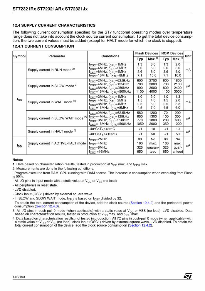
ST72321Rx ST72321ARx ST72321Jx
12.4 SUPPLY CURRENT CHARACTERISTICS
The following current consumption specified for the ST7 functional operating modes over temperaturerange does not take into account the clock source current consumption. To get the total device consump-tion, the two current values must be added (except for HALT mode for which the clock is stopped).
12.4.1 CURRENT CONSUMPTION
Notes:1. Data based on characterization results, tested in production at VDD max. and fCPU max.2. Measurements are done in the following conditions:- Program executed from RAM, CPU running with RAM access. The increase in consumption when executing from Flashis 50%.- All I/O pins in input mode with a static value at VDD or VSS (no load)- All peripherals in reset state.- LVD disabled.- Clock input (OSC1) driven by external square wave.- In SLOW and SLOW WAIT mode, fCPU is based on fOSC divided by 32.
To obtain the total current consumption of the device, add the clock source (Section 12.4.2) and the peripheral powerconsumption (Section 12.4.3).
3. All I/O pins in push-pull 0 mode (when applicable) with a static value at VDD or VSS (no load), LVD disabled. Databased on characterization results, tested in production at VDD max. and fCPU max.
4. Data based on characterisation results, not tested in production. All I/O pins in push-pull 0 mode (when applicable) witha static value at VDD or VSS (no load); clock input (OSC1) driven by external square wave, LVD disabled. To obtain thetotal current consumption of the device, add the clock source consumption (Section 12.4.2).
Symbol Parameter ConditionsFlash Devices ROM Devices
UnitTyp Max 1) Typ Max 1)
IDD
Supply current in RUN mode 2)
fOSC=2MHz, fCPU=1MHzfOSC=4MHz, fCPU=2MHzfOSC=8MHz, fCPU=4MHzfOSC=16MHz, fCPU=8MHz
1.32.03.67.1
3.05.08.015.0
1.32.03.67.1
2.03.05.0
10.0
mA
Supply current in SLOW mode 2)
fOSC=2MHz, fCPU=62.5kHzfOSC=4MHz, fCPU=125kHzfOSC=8MHz, fCPU=250kHzfOSC=16MHz, fCPU=500kHz
6007008001100
2700300036004000
6007008001100
1800210024003000
μA
Supply current in WAIT mode 2)
fOSC=2MHz, fCPU=1MHzfOSC=4MHz, fCPU=2MHzfOSC=8MHz, fCPU=4MHzfOSC=16MHz, fCPU=8MHz
1.01.52.54.5
3.04.05.07.0
1.01.52.54.5
1.32.03.36.0
mA
Supply current in SLOW WAIT mode 2)
fOSC=2MHz, fCPU=62.5kHzfOSC=4MHz, fCPU=125kHzfOSC=8MHz, fCPU=250kHzfOSC=16MHz, fCPU=500kHz
5806507701050
1200130018002000
70100200350
2003006001200
μA
Supply current in HALT mode 3) -40°C≤TA≤+85°C <1 10 <1 10μA
-40°C≤TA≤+125°C <1 50 <1 50
IDDSupply current in ACTIVE-HALT mode 4)
fOSC=2MHzfOSC=4MHz fOSC=8MHzfOSC =16MHz
80160325650
No max.
guaran-teed
80160325650
No max. guar-
anteed
μA
142/193
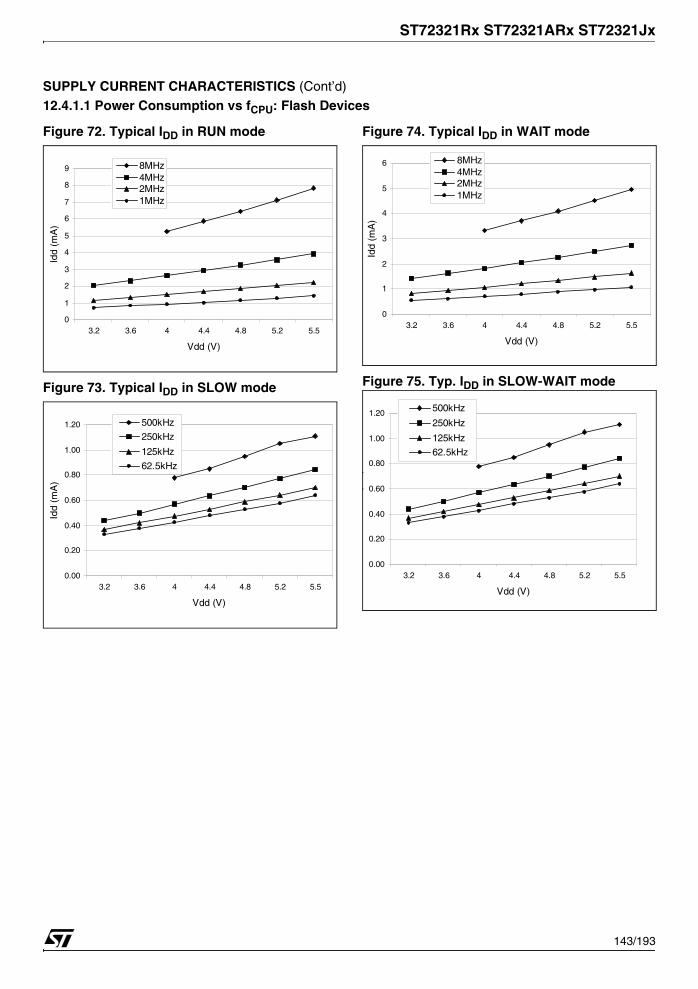
ST72321Rx ST72321ARx ST72321Jx
SUPPLY CURRENT CHARACTERISTICS (Cont’d)
12.4.1.1 Power Consumption vs fCPU: Flash Devices
Figure 72. Typical IDD in RUN mode
Figure 73. Typical IDD in SLOW mode
Figure 74. Typical IDD in WAIT mode
Figure 75. Typ. IDD in SLOW-WAIT mode
0
1
2
3
4
5
6
7
8
9
3.2 3.6 4 4.4 4.8 5.2 5.5
Vdd (V)
Idd
(mA
)
8MHz4MHz2MHz1MHz
0.00
0.20
0.40
0.60
0.80
1.00
1.20
3.2 3.6 4 4.4 4.8 5.2 5.5
Vdd (V)
Idd
(mA
)
500kHz
250kHz
125kHz
62.5kHz
0
1
2
3
4
5
6
3.2 3.6 4 4.4 4.8 5.2 5.5
Vdd (V)
Idd
(mA
)
8MHz4MHz2MHz1MHz
0.00
0.20
0.40
0.60
0.80
1.00
1.20
3.2 3.6 4 4.4 4.8 5.2 5.5
Vdd (V)
()
500kHz
250kHz
125kHz
62.5kHz
143/193

ST72321Rx ST72321ARx ST72321Jx
SUPPLY CURRENT CHARACTERISTICS (Cont’d)
12.4.2 Supply and Clock ManagersThe previous current consumption specified for the ST7 functional operating modes over temperaturerange does not take into account the clock source current consumption. To get the total device consump-tion, the two current values must be added (except for HALT mode).
Notes:1.. Data based on characterization results done with the external components specified in Section 12.5.3, not tested inproduction.2. As the oscillator is based on a current source, the consumption does not depend on the voltage.
Symbol Parameter Conditions Typ Max Unit
IDD(RCINT) Supply current of internal RC oscillator 625
μA
IDD(RES) Supply current of resonator oscillator 1) & 2)see section
12.5.3 on page 147
IDD(PLL) PLL supply current VDD= 5V 360
IDD(LVD) LVD supply current VDD= 5V 150 300
144/193

ST72321Rx ST72321ARx ST72321Jx
SUPPLY CURRENT CHARACTERISTICS (Cont’d)
12.4.3 On-Chip PeripheralsMeasured on LQFP64 generic board TA = 25°C fCPU=4MHz.
Notes:1. Data based on a differential IDD measurement between reset configuration (timer counter running at fCPU/4) and timer
counter stopped (only TIMD bit set). Data valid for one timer.2. Data based on a differential IDD measurement between reset configuration (timer stopped) and timer counter enabled
(only TCE bit set).3. Data based on a differential IDD measurement between reset configuration (SPI disabled) and a permanent SPI master
communication at maximum speed (data sent equal to 55h).This measurement includes the pad toggling consumption.4. Data based on a differential IDD measurement between SCI low power state (SCID=1) and a permanent SCI data trans-
mit sequence. 5. Data based on a differential IDD measurement between reset configuration (I2C disabled) and a permanent I2C master
communication at 100kHz (data sent equal to 55h). This measurement include the pad toggling consumption (27kOhmexternal pull-up on clock and data lines).
6. Data based on a differential IDD measurement between reset configuration and continuous A/D conversions.
Symbol Parameter Conditions Typ Unit
IDD(TIM) 16-bit Timer supply current 1) VDD=5.0V 50 μA
IDD(ART) ART PWM supply current2) VDD=5.0V 75 μA
IDD(SPI) SPI supply current 3) VDD=5.0V 400 μA
IDD(SCI) SCI supply current 4) VDD=5.0V 400 μA
IDD(I2C) I2C supply current 5) VDD=5.0V 175 μA
IDD(ADC) ADC supply current when converting 6) VDD=5.0V 400 μA
145/193
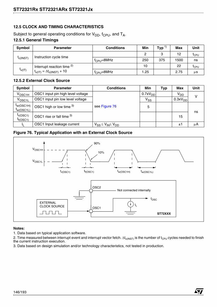
ST72321Rx ST72321ARx ST72321Jx
12.5 CLOCK AND TIMING CHARACTERISTICS
Subject to general operating conditions for VDD, fCPU, and TA.
12.5.1 General Timings
12.5.2 External Clock Source
Figure 76. Typical Application with an External Clock Source
Notes:1. Data based on typical application software.2. Time measured between interrupt event and interrupt vector fetch. Δtc(INST) is the number of tCPU cycles needed to finishthe current instruction execution.3. Data based on design simulation and/or technology characteristics, not tested in production.
Symbol Parameter Conditions Min Typ 1) Max Unit
tc(INST) Instruction cycle time2 3 12 tCPU
fCPU=8MHz 250 375 1500 ns
tv(IT)Interrupt reaction time 2)
tv(IT) = Δtc(INST) + 1010 22 tCPU
fCPU=8MHz 1.25 2.75 μs
Symbol Parameter Conditions Min Typ Max Unit
VOSC1H OSC1 input pin high level voltage
see Figure 76
0.7xVDD VDD VVOSC1L OSC1 input pin low level voltage VSS 0.3xVDD
tw(OSC1H)tw(OSC1L)
OSC1 high or low time 3) 5ns
tr(OSC1)tf(OSC1)
OSC1 rise or fall time 3) 15
IL OSC1 Input leakage current VSS ≤ VIN≤ VDD ±1 μA
OSC1
OSC2
fOSCEXTERNAL
ST72XXX
CLOCK SOURCE
Not connected internally
VOSC1L
VOSC1H
tr(OSC1) tf(OSC1) tw(OSC1H) tw(OSC1L)
IL
90%
10%
146/193

ST72321Rx ST72321ARx ST72321Jx
CLOCK AND TIMING CHARACTERISTICS (Cont’d)
12.5.3 Crystal and Ceramic Resonator OscillatorsThe ST7 internal clock can be supplied with fourdifferent Crystal/Ceramic resonator oscillators. Allthe information given in this paragraph is based oncharacterization results with specified typical ex-ternal components. In the application, the resona-tor and the load capacitors have to be placed as
close as possible to the oscillator pins in order tominimize output distortion and start-up stabiliza-tion time. Refer to the crystal/ceramic resonatormanufacturer for more details (frequency, pack-age, accuracy...).
Notes:1. The oscillator selection can be optimized in terms of supply current using an high quality resonator with small RS value.Refer to crystal/ceramic resonator manufacturer for more details.2. Data based on characterisation results, not tested in production.
Symbol Parameter Conditions Min Max Unit
fOSC Oscillator Frequency 1)
LP: Low power oscillatorMP: Medium power oscillatorMS: Medium speed oscillatorHS: High speed oscillator
1>2>4>8
24816
MHz
RF Feedback resistor2) 20 40 kΩ
CL1
CL2
Recommended load capacitance ver-sus equivalent serial resistance of the crystal or ceramic resonator (RS)
RS=200Ω LP oscillatorRS=200Ω MP oscillatorRS=200Ω MS oscillatorRS=100Ω HS oscillator
22221815
56463333
pF
Symbol Parameter Conditions Typ Max Unit
i2 OSC2 driving current
VDD=5V LP oscillatorVIN=VSS MP oscillator
MS oscillatorHS oscillator
80160310610
150250460910
μA
147/193
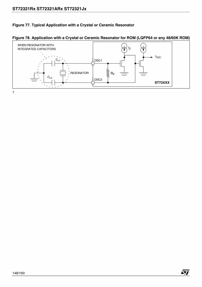
ST72321Rx ST72321ARx ST72321Jx
Figure 77. Typical Application with a Crystal or Ceramic Resonator
Figure 78. Application with a Crystal or Ceramic Resonator for ROM (LQFP64 or any 48/60K ROM)
1
OSC2
OSC1fOSC
CL1
CL2
i2
RF
ST72XXX
RESONATOR
WHEN RESONATOR WITHINTEGRATED CAPACITORS
148/193

ST72321Rx ST72321ARx ST72321Jx
CLOCK AND TIMING CHARACTERISTICS (Cont’d)
Notes:1. Resonator characteristics given by the ceramic resonator manufacturer.2. SMD = [-R0: Plastic tape package (∅ =180mm), -B0: Bulk]
LEAD = [-A0: Flat pack package (Radial taping Ho= 18mm), -B0: Bulk]3. LP mode is not recommended for 2 MHz resonator because the peak to peak amplitude is too small (>0.8V)For more information on these resonators, please consult www.murata.com
SupplierfOSC
(MHz)
Typical Ceramic Resonators1)
Reference2) Recommended OSCRANGE Option bit configuration
Mur
ata
2 CSTCC2M00G56A-R0 MP Mode3)
4 CSTCR4M00G55B-R0 MS Mode
8 CSTCE8M00G55A-R0 HS Mode
16 CSTCE16M0G53A-R0 HS Mode
149/193

ST72321Rx ST72321ARx ST72321Jx
CLOCK CHARACTERISTICS (Cont’d)
12.5.4 RC Oscillators
Figure 79. Typical fOSC(RCINT) vs TA Note: To reduce disturbance to the RC oscillator,it is recommended to place decoupling capacitorsbetween VDD and VSS as shown in Figure 99
Symbol Parameter Conditions Min Typ Max Unit
fOSC (RCINT)Internal RC oscillator frequency
See Figure 79 TA=25°C, VDD=5V 2 3.5 5.6 MHz
3
3.2
3.4
3.6
3.8
4
-45 0 25 70 130
TA(°C)
fOS
C(R
CIN
T) (
MH
z) Vdd = 5VVdd = 5.5V
150/193

ST72321Rx ST72321ARx ST72321Jx
CLOCK CHARACTERISTICS (Cont’d)Note:1. Data based on characterization results.
12.5.5 PLL Characteristics
Note:1. Data characterized but not tested.
The user must take the PLL jitter into account in the application (for example in serial communication orsampling of high frequency signals). The PLL jitter is a periodic effect, which is integrated over severalCPU cycles. Therefore the longer the period of the application signal, the less it will be impacted by thePLL jitter.
Figure 80 shows the PLL jitter integrated on application signals in the range 125kHz to 4MHz. At frequen-cies of less than 125KHz, the jitter is negligible.
Figure 80. Integrated PLL Jitter vs signal frequency1
Note 1: Measurement conditions: fCPU = 8MHz.
Symbol Parameter Conditions Min Typ Max Unit
fOSC PLL input frequency range 2 4 MHz
Δ fCPU/ fCPUInstantaneous PLL jitter 1) fOSC = 4 MHz. 1.0 2.5 %
fOSC = 2 MHz. 2.5 4.0
00.10.20.30.40.50.60.70.8
4 MHz 2 MHz 1 MHz 500 kHz 250 kHzApplication Frequency
+/-Jitter (%)
151/193
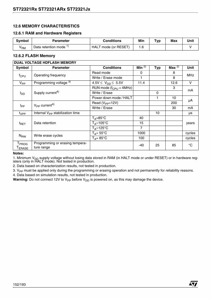
ST72321Rx ST72321ARx ST72321Jx
12.6 MEMORY CHARACTERISTICS
12.6.1 RAM and Hardware Registers
12.6.2 FLASH Memory
Notes:1. Minimum VDD supply voltage without losing data stored in RAM (in HALT mode or under RESET) or in hardware reg-isters (only in HALT mode). Not tested in production.2. Data based on characterization results, not tested in production.3. VPP must be applied only during the programming or erasing operation and not permanently for reliability reasons.4. Data based on simulation results, not tested in production.Warning: Do not connect 12V to VPP before VDD is powered on, as this may damage the device.
Symbol Parameter Conditions Min Typ Max Unit
VRM Data retention mode 1) HALT mode (or RESET) 1.6 V
DUAL VOLTAGE HDFLASH MEMORYSymbol Parameter Conditions Min 2) Typ Max 2) Unit
fCPU Operating frequencyRead mode 0 8
MHzWrite / Erase mode 1 8
VPP Programming voltage 3) 4.5V ≤ VDD ≤ 5.5V 11.4 12.6 V
IDD Supply current4)RUN mode (fCPU = 4MHz) 3
mAWrite / Erase 0Power down mode / HALT 1 10
µAIPP VPP current4) Read (VPP=12V) 200
Write / Erase 30 mAtVPP Internal VPP stabilization time 10 µs
tRET Data retentionTA=85°C 40
yearsTA=105°C 15TA=125°C 7
NRW Write erase cyclesTA= 55°C 1000 cyclesTA= 85°C 100 cycles
TPROGTERASE
Programming or erasing tempera-ture range
-40 25 85 °C
152/193

ST72321Rx ST72321ARx ST72321Jx
12.7 EMC CHARACTERISTICS
Susceptibility tests are performed on a sample ba-sis during product characterization.
12.7.1 Functional EMS (Electro MagneticSusceptibility)Based on a simple running application on theproduct (toggling 2 LEDs through I/O ports), theproduct is stressed by two electro magnetic eventsuntil a failure occurs (indicated by the LEDs).■ ESD: Electro-Static Discharge (positive and
negative) is applied on all pins of the device untila functional disturbance occurs. This testconforms with the IEC 1000-4-2 standard.
■ FTB: A Burst of Fast Transient voltage (positiveand negative) is applied to VDD and VSS througha 100pF capacitor, until a functional disturbanceoccurs. This test conforms with the IEC 1000-4-4 standard.
A device reset allows normal operations to be re-sumed. The test results are given in the table be-low based on the EMS levels and classes definedin application note AN1709.
12.7.1.1 Designing hardened software to avoidnoise problemsEMC characterization and optimization are per-formed at component level with a typical applica-
tion environment and simplified MCU software. Itshould be noted that good EMC performance ishighly dependent on the user application and thesoftware in particular.
Therefore it is recommended that the user appliesEMC software optimization and prequalificationtests in relation with the EMC level requested forhis application.
Software recommendations:The software flowchart must include the manage-ment of runaway conditions such as:
– Corrupted program counter
– Unexpected reset
– Critical Data corruption (control registers...)
Prequalification trials:Most of the common failures (unexpected resetand program counter corruption) can be repro-duced by manually forcing a low state on the RE-SET pin or the Oscillator pins for 1 second.
To complete these trials, ESD stress can be ap-plied directly on the device, over the range ofspecification values. When unexpected behaviouris detected, the software can be hardened to pre-vent unrecoverable errors occurring (see applica-tion note AN1015).
Symbol Parameter ConditionsLevel/Class
VFESDVoltage limits to be applied on any I/O pin to induce a functional disturbance
Flash device: VDD=5V, TA=+25°C, fOSC=8MHz conforms to IEC 1000-4-2
4B
ROM device: VDD=5V, TA=+25°C, fOSC=8 MHz, conforms to IEC 1000-4-2
4A
VFFTB
Fast transient voltage burst limits to be applied through 100pF on VDD and VDD pins to induce a func-tional disturbance
VDD=5V, TA=+25°C, fOSC=8 MHz, con-forms to IEC 1000-4-4
3B
VFFTB
Fast transient voltage burst limits to be applied through 100pF on VDD and VDD pins to induce a func-tional disturbance
VDD=5V, TA=+25°C, fOSC=8 MHz, con-forms to IEC 1000-4-4
3B
153/193

ST72321Rx ST72321ARx ST72321Jx
EMC CHARACTERISTICS (Cont’d)
12.7.2 Electro Magnetic Interference (EMI)Based on a simple application running on theproduct (toggling 2 LEDs through the I/O ports),the product is monitored in terms of emission. Thisemission test is in line with the norm SAE J 1752/3 which specifies the board and the loading ofeach pin.
Notes:1. Data based on characterization results, not tested in production.2. Refer to Application Note AN1709 for data on other package types.
Symbol Parameter ConditionsMonitored
Frequency BandMax vs. [fOSC/fCPU]1 Unit
8/4MHz 16/8MHz
SEMI Peak level VDD=5V, TA=+25°C,LQFP64 10x10 packageconforming to SAE J 1752/3
0.1MHz to 30MHz 15 20
dBμV30MHz to 130MHz 20 27
130MHz to 1GHz 7 12
SAE EMI Level 2.5 3 -
SEMI Peak level
60K ROM Devices: VDD=5V, TA=+25°C,LQFP64 packageconforming to SAE J 1752/3
0.1MHz to 30MHz 15 20
dBμV30MHz to 130MHz 20 27
130MHz to 1GHz 7 12
SAE EMI Level 2.5 3 -
SEMI Peak level
8/16/32K ROM devices: VDD=5V, TA=+25°C,LQFP44 10x10 package conforming to SAE J 1752/3
0.1MHz to 30MHz 17 21
dBμV30MHz to 130MHz 24 30
130MHz to 1GHz 18 23
SAE EMI Level 3 3.5 -
154/193
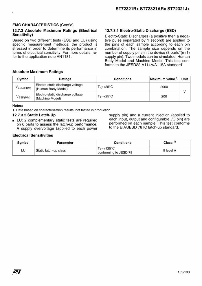
ST72321Rx ST72321ARx ST72321Jx
EMC CHARACTERISTICS (Cont’d)
12.7.3 Absolute Maximum Ratings (ElectricalSensitivity)Based on two different tests (ESD and LU) usingspecific measurement methods, the product isstressed in order to determine its performance interms of electrical sensitivity. For more details, re-fer to the application note AN1181.
12.7.3.1 Electro-Static Discharge (ESD)Electro-Static Discharges (a positive then a nega-tive pulse separated by 1 second) are applied tothe pins of each sample according to each pincombination. The sample size depends on thenumber of supply pins in the device (3 parts*(n+1)supply pin). Two models can be simulated: HumanBody Model and Machine Model. This test con-forms to the JESD22-A114A/A115A standard.
Absolute Maximum Ratings
Notes:1. Data based on characterization results, not tested in production.
12.7.3.2 Static Latch-Up■ LU: 2 complementary static tests are required
on 6 parts to assess the latch-up performance.A supply overvoltage (applied to each power
supply pin) and a current injection (applied toeach input, output and configurable I/O pin) areperformed on each sample. This test conformsto the EIA/JESD 78 IC latch-up standard.
Electrical Sensitivities
Symbol Ratings Conditions Maximum value 1) Unit
VESD(HBM)Electro-static discharge voltage(Human Body Model)
TA=+25°C 2000V
VESD(MM)Electro-static discharge voltage(Machine Model)
TA=+25°C 200
Symbol Parameter Conditions Class 1)
LU Static latch-up classTA=+125°C conforming to JESD 78
II level A
155/193

ST72321Rx ST72321ARx ST72321Jx
12.8 I/O PORT PIN CHARACTERISTICS
12.8.1 General CharacteristicsSubject to general operating conditions for VDD, fOSC, and TA unless otherwise specified.
Figure 81. Unused I/Os configured as input Figure 82. Typical IPU vs. VDD with VIN=VSS
Notes:1. Data based on characterization results, not tested in production.2. Hysteresis voltage between Schmitt trigger switching levels. Based on characterization results, not tested.3. When the current limitation is not possible, the VIN maximum must be respected, otherwise refer to IINJ(PIN) specifica-tion. A positive injection is induced by VIN>VDD while a negative injection is induced by VIN<VSS. Refer to section 12.2.2on page 139 for more details.4. Configuration not recommended, all unused pins must be kept at a fixed voltage: using the output mode of the I/O forexample and leaving the I/O unconnected on the board or an external pull-up or pull-down resistor (see Figure 81). Staticpeak current value taken at a fixed VIN value, based on design simulation and technology characteristics, not tested inproduction. This value depends on VDD and temperature values.5. The RPU pull-up equivalent resistor is based on a resistive transistor (corresponding IPU current characteristics de-scribed in Figure 82). 6. To generate an external interrupt, a minimum pulse width has to be applied on an I/O port pin configured as an externalinterrupt source.
Symbol Parameter Conditions Min Typ Max Unit
VIL Input low level voltage 1)
CMOS ports
0.3xVDD
VVIH Input high level voltage 1) 0.7xVDD
Vhys Schmitt trigger voltage hysteresis 2) 0.7
IINJ(PIN)3)
Injected Current on PC6 (Flash de-vices only)
VDD=5V
0 +4
mAInjected Current on an I/O pin ± 4
ΣIINJ(PIN)3) Total injected current (sum of all I/O
and control pins) ± 25
IL Input leakage current VSS≤ VIN ≤ VDD ±1μA
IS Static current consumption Floating input mode 4) 400
RPU Weak pull-up equivalent resistor 5) VIN=VSS VDD=5V 50 120 250 kΩ
CIO I/O pin capacitance 5 pF
tf(IO)out Output high to low level fall time 1)CL=50pFBetween 10% and 90%
25ns
tr(IO)out Output low to high level rise time 1) 25
tw(IT)in External interrupt pulse time 6) 1 tCPU
10kΩ
ST7XXX
10kΩ
UNUSED I/O PORT
ST7XXXVDD
Note: I/O can be left unconnected if it is configured as output
greater EMC robustness and lower cost.(0 or 1) by the software. This has the advantage of
UNUSED I/O PORT
0
10
20
30
40
50
60
70
80
90
2 2.5 3 3.5 4 4.5 5 5.5 6Vdd(V)
Ipu(
uA)
Ta=140°C
Ta=95°C
Ta=25°C
Ta=-45°C
156/193

ST72321Rx ST72321ARx ST72321Jx
I/O PORT PIN CHARACTERISTICS (Cont’d)
12.8.2 Output Driving Current Subject to general operating conditions for VDD, fCPU, and TA unless otherwise specified.
Figure 83. Typical VOL at VDD=5V (standard)
Figure 84. Typical VOL at VDD=5V (high-sink)
Figure 85. Typical VOH at VDD=5V
Notes:1. The IIO current sunk must always respect the absolute maximum rating specified in Section 12.2.2 and the sum of IIO(I/O ports and control pins) must not exceed IVSS.2. The IIO current sourced must always respect the absolute maximum rating specified in Section 12.2.2 and the sum ofIIO (I/O ports and control pins) must not exceed IVDD. True open drain I/O pins do not have VOH.
Symbol Parameter Conditions Min Max Unit
VOL 1)
Output low level voltage for a standard I/O pin when 8 pins are sunk at same time(see Figure 83)
VD
D=
5V
IIO=+5mA 1.2
V
IIO=+2mA 0.5
Output low level voltage for a high sink I/O pin when 4 pins are sunk at same time(see Figure 84 and Figure 86)
IIO=+20mA,TA≤ 85°CTA≥85°C
1.31.5
IIO=+8mA 0.6
VOH 2)
Output high level voltage for an I/O pinwhen 4 pins are sourced at same time(see Figure 85 and Figure 88)
IIO=-5mA, TA≤ 85°CTA≥85°C
VDD-1.4VDD-1.6
IIO=-2mA VDD-0.7
0
0.2
0.4
0.6
0.8
1
1.2
1.4
0 0.005 0.01 0.015Iio(A)
Vol
(V) a
t Vdd
=5V
Ta=140°C "
Ta=95°C
Ta=25°C
Ta=-45°C
0
0.1
0.2
0.3
0.4
0.5
0.6
0.7
0.8
0.9
1
0 0.01 0.02 0.03
Iio(A)
Vol
(V) a
t Vdd
=5V
Ta= 140°C
Ta= 95°C
Ta= 25°C
Ta= -45°C
2
2.5
3
3.5
4
4.5
5
5.5
-0.01 -0.008 -0.006 -0.004 -0.002 0
Vdd
-Voh
(V) a
t Vdd
=5V
V dd= 5V 140°C m in
V dd= 5v 95°C m in
V dd= 5v 25°C m in
V dd= 5v -45°C m in
157/193

ST72321Rx ST72321ARx ST72321Jx
I/O PORT PIN CHARACTERISTICS (Cont’d)
Figure 86. Typical VOL vs. VDD (standard)
Figure 87. Typical VOL vs. VDD (high-sink)
Figure 88. Typical VDD-VOH vs. VDD
0
0.1
0.2
0.3
0.4
0.5
0.6
0.7
0.8
0.9
1
2 2.5 3 3.5 4 4.5 5 5.5 6
Vdd(V)
Vol
(V) a
t Iio
=5m
A
Ta= -45°C
Ta= 25°C
Ta= 95°C
Ta= 140°C
0
0.05
0.1
0.15
0.2
0.25
0.3
0.35
0.4
0.45
2 2.5 3 3.5 4 4.5 5 5.5 6Vdd(V)
Vol
(V) a
t Iio
=2m
A
Ta=-45°C
Ta=25°C
Ta=95°C
Ta=140°C
0
0.1
0 .2
0 .3
0 .4
0 .5
0 .6
2 2.5 3 3.5 4 4.5 5 5.5 6
Vdd(V )
Vol
(V)
at Ii
o=8m
A
Ta= 140°C
Ta=95°C
Ta=25°C
Ta=-45°C
0
0 .2
0 .4
0 .6
0 .8
1
1 .2
1 .4
1 .6
2 2.5 3 3.5 4 4.5 5 5.5 6
V dd(V )
Vol
(V)
at Ii
o=20
mA
Ta= 140°C
Ta=95°C
Ta=25°C
Ta=-45°C
0
1
2
3
4
5
6
2 2.5 3 3.5 4 4.5 5 5.5 6
Vdd(V)
Vdd
-Voh
(V)
at Ii
o=-5
mA
Ta= -45°C
Ta= 25°C
Ta= 95°C
Ta= 140°C
2
2.5
3
3.5
4
4.5
5
5.5
2 2.5 3 3.5 4 4.5 5 5.5 6
Vdd(V)
Vdd
-Voh
(V) a
t Iio
=-2m
A
Ta= -45°C
Ta= 25°C
Ta= 95°C
Ta= 140°C
158/193

ST72321Rx ST72321ARx ST72321Jx
12.9 CONTROL PIN CHARACTERISTICS
12.9.1 Asynchronous RESET PinSubject to general operating conditions for VDD, fCPU, and TA unless otherwise specified.
Notes:1. Data based on characterization results, not tested in production.2. Hysteresis voltage between Schmitt trigger switching levels.3. The IIO current sunk must always respect the absolute maximum rating specified in Section 12.2.2 and the sum of IIO(I/O ports and control pins) must not exceed IVSS.4. To guarantee the reset of the device, a minimum pulse has to be applied to the RESET pin. All short pulses applied onthe RESET pin with a duration below th(RSTL)in can be ignored.5. The reset network (the resistor and two capacitors) protects the device against parasitic resets, especially in noisy en-vironments.6. Data guaranteed by design, not tested in production.
Symbol Parameter Conditions Min Typ Max Unit
VIL Input low level voltage 1) 0.16xVDD VVIH Input high level voltage 1) 0.85xVDD
Vhys Schmitt trigger voltage hysteresis 2) 2.5V
VOL Output low level voltage 3) VDD=5V IIO=+2mA 0.2 0.5
IIO Input current on RESET pin 2 mA
RON Weak pull-up equivalent resistor 20 30 120 kΩ
tw(RSTL)out Generated reset pulse durationStretch applied on external pulse
0 426) μs
Internal reset sources 20 30 426) μs
th(RSTL)in External reset pulse hold time 4) 2.5 μs
tg(RSTL)in Filtered glitch duration 5) 200 ns
159/193

ST72321Rx ST72321ARx ST72321Jx
CONTROL PIN CHARACTERISTICS (Cont’d)
Figure 89. RESET pin protection when LVD is enabled.1)2)3)4)
Figure 90. RESET pin protection when LVD is disabled.1)
Note 1:– The reset network protects the device against parasitic resets.– The output of the external reset circuit must have an open-drain output to drive the ST7 reset pad. Otherwise the
device can be damaged when the ST7 generates an internal reset (LVD or watchdog).– Whatever the reset source is (internal or external), the user must ensure that the level on the RESET pin can go
below the VIL max. level specified in section 12.9.1 on page 159. Otherwise the reset will not be taken into accountinternally.
– Because the reset circuit is designed to allow the internal RESET to be output in the RESET pin, the user must en-sure that the current sunk on the RESET pin is less than the absolute maximum value specified for IINJ(RESET) insection 12.2.2 on page 139.
Note 2: When the LVD is enabled, it is recommended not to connect a pull-up resistor or capacitor. A 10nF pull-downcapacitor is required to filter noise on the reset line.Note 3: In case a capacitive power supply is used, it is recommended to connect a 1MΩ pull-down resistor to the RESETpin to discharge any residual voltage induced by the capacitive effect of the power supply (this will add 5µA to the powerconsumption of the MCU).Note 4: Tips when using the LVD:
– 1. Check that all recommendations related to reset circuit have been applied (see notes above).– 2. Check that the power supply is properly decoupled (100nF + 10µF close to the MCU). Refer to AN1709 and
AN2017. If this cannot be done, it is recommended to put a 100nF + 1MΩ pull-down on the RESET pin.– 3. The capacitors connected on the RESET pin and also the power supply are key to avoid any start-up marginality.
In most cases, steps 1 and 2 above are sufficient for a robust solution. Otherwise: replace 10nF pull-down on theRESET pin with a 5µF to 20µF capacitor.
0.01μF
ST72XXX
PULSEGENERATOR
Filter
RON
VDD
WATCHDOG
LVD RESET
INTERNALRESET
RESETEXTERNAL
Required
1MΩ
Optional (note 3)
0.01μF
EXTERNALRESET
CIRCUIT
USER
Required
ST72XXX
PULSEGENERATOR
Filter
RON
VDD
WATCHDOG
INTERNALRESET
160/193

ST72321Rx ST72321ARx ST72321Jx
CONTROL PIN CHARACTERISTICS (Cont’d)
12.9.2 ICCSEL/VPP PinSubject to general operating conditions for VDD, fCPU, and TA unless otherwise specified.
Figure 91. Two typical Applications with ICCSEL/VPP Pin 2)
Notes:1. Data based on design simulation and/or technology characteristics, not tested in production.2. When ICC mode is not required by the application ICCSEL/VPP pin must be tied to VSS.
Symbol Parameter Conditions Min Max1 Unit
VIL Input low level voltage 1) FLASH versions VSS 0.2
VROM versions VSS 0.3xVDD
VIH Input high level voltage 1) FLASH versions VDD-0.1 12.6
ROM versions 0.7xVDD VDD
IL Input leakage current VIN=VSS ±1 μA
ICCSEL/VPP
ST72XXX 10kΩ
PROGRAMMINGTOOL
VPP
ST72XXX
161/193

ST72321Rx ST72321ARx ST72321Jx
12.10 TIMER PERIPHERAL CHARACTERISTICS
Subject to general operating conditions for VDD, fOSC, and TA unless otherwise specified.
Refer to I/O port characteristics for more details on the input/output alternate function characteristics (out-put compare, input capture, external clock, PWM output...).
12.10.1 8-Bit PWM-ART Auto-Reload Timer
12.10.2 16-Bit Timer
Symbol Parameter Conditions Min Typ Max Unit
tres(PWM) PWM resolution time1 tCPU
fCPU=8MHz 125 ns
fEXT ART external clock frequency 0 fCPU/2MHz
fPWM PWM repetition rate 0 fCPU/2
ResPWM PWM resolution 8 bit
VOS PWM/DAC output step voltage VDD=5V, Res=8-bits 20 mV
Symbol Parameter Conditions Min Typ Max Unit
tw(ICAP)in Input capture pulse time 1 tCPU
tres(PWM) PWM resolution time2 tCPU
fCPU=8MHz 250 ns
fEXT Timer external clock frequency 0 fCPU/4 MHz
fPWM PWM repetition rate 0 fCPU/4 MHz
ResPWM PWM resolution 16 bit
162/193

ST72321Rx ST72321ARx ST72321Jx
12.11 COMMUNICATION INTERFACE CHARACTERISTICS
12.11.1 SPI - Serial Peripheral InterfaceSubject to general operating conditions for VDD,fCPU, and TA unless otherwise specified.
Refer to I/O port characteristics for more details onthe input/output alternate function characteristics(SS, SCK, MOSI, MISO).
Figure 92. SPI Slave Timing Diagram with CPHA=0 3)
Notes:1. Data based on design simulation and/or characterisation results, not tested in production.2. When no communication is on-going the data output line of the SPI (MOSI in master mode, MISO in slave mode) hasits alternate function capability released. In this case, the pin status depends on the I/O port configuration.3. Measurement points are done at CMOS levels: 0.3xVDD and 0.7xVDD.4. Depends on fCPU. For example, if fCPU = 8 MHz, then tCPU = 1 / fCPU = 125 ns and tsu(SS) = 175 ns.
Symbol Parameter Conditions Min Max Unit
fSCK1/tc(SCK)
SPI clock frequency
MasterfCPU=8MHz
fCPU/1280.0625
fCPU/42
MHzSlavefCPU=8MHz
0fCPU/2
4
tr(SCK)tf(SCK)
SPI clock rise and fall time see I/O port pin description
tsu(SS) SS setup time4) Slave tCPU + 50
ns
th(SS) SS hold time Slave 120
tw(SCKH)tw(SCKL)
SCK high and low timeMasterSlave
10090
tsu(MI)tsu(SI)
Data input setup timeMasterSlave
100100
th(MI)th(SI)
Data input hold timeMasterSlave
100100
ta(SO) Data output access time Slave 0 120
tdis(SO) Data output disable time Slave 240
tv(SO) Data output valid timeSlave (after enable edge)
120
th(SO) Data output hold time 0
tv(MO) Data output valid timeMaster (after enable edge)
120tCPUth(MO) Data output hold time 0
SS INPUT
SC
KIN
PU
T CPHA=0
MOSI INPUT
MISO OUTPUT
CPHA=0
tc(SCK)
tw(SCKH)tw(SCKL) tr(SCK)
tf(SCK)
tv(SO)ta(SO)
tsu(SI) th(SI)
MSB OUT
MSB IN
BIT6 OUT
LSB IN
LSB OUTsee note 2
CPOL=0
CPOL=1
tsu(SS) th(SS)
tdis(SO)th(SO)
seenote 2
BIT1 IN
163/193

ST72321Rx ST72321ARx ST72321Jx
COMMUNICATION INTERFACE CHARACTERISTICS (Cont’d)
Figure 93. SPI Slave Timing Diagram with CPHA=11)
Figure 94. SPI Master Timing Diagram 1)
Notes:1. Measurement points are done at CMOS levels: 0.3xVDD and 0.7xVDD.2. When no communication is on-going the data output line of the SPI (MOSI in master mode, MISO in slave mode) hasits alternate function capability released. In this case, the pin status depends of the I/O port configuration.
SS INPUT
SC
KIN
PU
T CPHA=1
MOSI INPUT
MISO OUTPUT
CPHA=1
tw(SCKH)tw(SCKL) tr(SCK)
tf(SCK)
ta(SO)
tsu(SI) th(SI)
MSB OUT BIT6 OUT LSB OUTsee
CPOL=0
CPOL=1
tsu(SS) th(SS)
tdis(SO)th(SO)
seenote 2note 2
tc(SCK)
HZ
tv(SO)
MSB IN LSB INBIT1 IN
SS INPUT
SC
KIN
PU
T
CPHA = 0
MOSI OUTPUT
MISO INPUT
CPHA = 0
CPHA = 1
CPHA = 1
tc(SCK)
tw(SCKH)tw(SCKL)
th(MI)tsu(MI)
MSB IN
MSB OUT
BIT6 IN
BIT6 OUT LSB OUT
LSB IN
See note 2 See note 2
CPOL = 0
CPOL = 1
CPOL = 0
CPOL = 1
tr(SCK)tf(SCK)
th(MO)tv(MO)
164/193

ST72321Rx ST72321ARx ST72321Jx
COMMUNICATION INTERFACE CHARACTERISTICS (Cont’d)
12.11.2 I2C - Inter IC Control InterfaceSubject to general operating conditions for VDD,fCPU, and TA unless otherwise specified.
Refer to I/O port characteristics for more details onthe input/output alternate function characteristics(SDAI and SCLI). The ST7 I2C interface meets therequirements of the Standard I2C communicationprotocol described in the following table.
Figure 95. Typical Application with I2C Bus and Timing Diagram 4)
Notes:1. Data based on standard I2C protocol requirement, not tested in production.2. The device must internally provide a hold time of at least 300ns for the SDA signal in order to bridge the undefinedregion of the falling edge of SCL.3. The maximum hold time of the START condition has only to be met if the interface does not stretch the low period ofSCL signal.4. Measurement points are done at CMOS levels: 0.3xVDD and 0.7xVDD.5. At 4MHz fCPU, max.I2C speed (400kHz) is not achievable. In this case, max. I2C speed will be approximately 260KHz.
Symbol ParameterStandard mode I2C Fast mode I2C5)
UnitMin 1) Max 1) Min 1) Max 1)
tw(SCLL) SCL clock low time 4.7 1.3 μs
tw(SCLH) SCL clock high time 4.0 0.6
tsu(SDA) SDA setup time 250 100
ns
th(SDA) SDA data hold time 0 3) 0 2) 900 3)
tr(SDA)tr(SCL)
SDA and SCL rise time 1000 20+0.1Cb 300
tf(SDA)tf(SCL)
SDA and SCL fall time 300 20+0.1Cb 300
th(STA) START condition hold time 4.0 0.6μs
tsu(STA) Repeated START condition setup time 4.7 0.6
tsu(STO) STOP condition setup time 4.0 0.6 μs
tw(STO:STA) STOP to START condition time (bus free) 4.7 1.3 μs
Cb Capacitive load for each bus line 400 400 pF
REPEATED START
START
STOP
START
tf(SDA) tr(SDA) tsu(SDA) th(SDA)
tf(SCK)tr(SCK)tw(SCKL)tw(SCKH)th(STA) tsu(STO)
tsu(STA) tw(STO:STA)
SDA
SCK
4.7kΩSDAI
ST72XXXSCLI
VDD
100Ω
100Ω
VDD
4.7kΩ
I2C BUS
165/193

ST72321Rx ST72321ARx ST72321Jx
COMMUNICATION INTERFACE CHARACTERISTICS (Cont’d)The following table gives the values to be written inthe I2CCCR register to obtain the required I2CSCL line frequency.
Table 28. SCL Frequency Table
Legend:RP = External pull-up resistance
fSCL = I2C speed
NA = Not achievable
Note:– For speeds around 200 kHz, achieved speed can have ±5% tolerance
– For other speed ranges, achieved speed can have ±2% tolerance
The above variations depend on the accuracy of the external components used.
fSCL
(kHz)
I2CCCR ValuefCPU=4 MHz. fCPU=8 MHz.
VDD = 4.1 V VDD = 5 V VDD = 4.1 V VDD = 5 VRP=3.3kΩ RP=4.7kΩ RP=3.3kΩ RP=4.7kΩ RP=3.3kΩ RP=4.7kΩ RP=3.3kΩ RP=4.7kΩ
400 NA NA NA NA 83h 83 83h 83h300 NA NA NA NA 85h 85h 85h 85h200 83h 83h 83h 83h 8Ah 89h 8Ah 8Ah100 10h 10h 10h 10h 24h 23h 24h 23h50 24h 24h 24h 24h 4Ch 4Ch 4Ch 4Ch20 5Fh 5Fh 5Fh 5Fh FFh FFh FFh FFh
166/193

ST72321Rx ST72321ARx ST72321Jx
12.12 10-BIT ADC CHARACTERISTICS
Subject to general operating conditions for VDD, fCPU, and TA unless otherwise specified.
Notes:1. Any added external serial resistor will downgrade the ADC accuracy (especially for resistance greater than 10kΩ). Databased on characterization results, not tested in production.2. Injecting negative current on any of the analog input pins significantly reduces the accuracy of any conversion beingperformed on any analog input. Analog pins can be protected against negative injection by adding a Schottky diode (pinto ground). Injecting negative current on digital input pins degrades ADC accuracy especially if performed on a pin closeto the analog input pins. Any positive injection current within the limits specified for IINJ(PIN) and ΣIINJ(PIN) in Section 12.8does not affect the ADC accuracy.
Symbol Parameter Conditions Min Typ Max Unit
fADC ADC clock frequency 0.4 2 MHz
VAREF Analog reference voltage 0.7*VDD ≤ VAREF ≤ VDD 3.8 VDD VVAIN Conversion voltage range 1) VSSA VAREF
RAIN External input impedance see Figure 96
and Figure 97
kΩ
CAIN External capacitor on analog input pF
fAIN Variation freq. of analog input signal Hz
CADC Internal sample and hold capacitor 12 pF
tADCConversion time (Sample+Hold) fCPU=8MHz, SPEED=0 fADC=2MHz
7.5 μs
tADC- No of sample capacitor loading cycles- No. of Hold conversion cycles
411
1/fADC
167/193

ST72321Rx ST72321ARx ST72321Jx
ADC CHARACTERISTICS (Cont’d)
Figure 96. RAIN max. vs fADC with CAIN=0pF1) Figure 97. Recommended CAIN & RAIN values.2)
Figure 98. Typical A/D Converter Application
Notes:1. CPARASITIC represents the capacitance of the PCB (dependent on soldering and PCB layout quality) plus the pad ca-pacitance (3pF). A high CPARASITIC value will downgrade conversion accuracy. To remedy this, fADC should be reduced.2. This graph shows that depending on the input signal variation (fAIN), CAIN can be increased for stabilization time anddecreased to allow the use of a larger serial resistor (RAIN).
0
5
10
15
20
25
30
35
40
45
0 10 30 70
CPARASITIC (pF)
Max
. RA
IN (
Koh
m)
2 MHz
1 MHz
0.1
1
10
100
1000
0.01 0.1 1 10
fAIN(KHz)
Max
. RA
IN (
Koh
m)
Cain 10 nF
Cain 22 nF
Cain 47 nF
AINx
ST72XXXVDD
IL±1μA
VT0.6V
VT0.6V CADC
12pF
VAIN
RAIN 10-Bit A/D Conversion
2kΩ(max)
CAIN
168/193
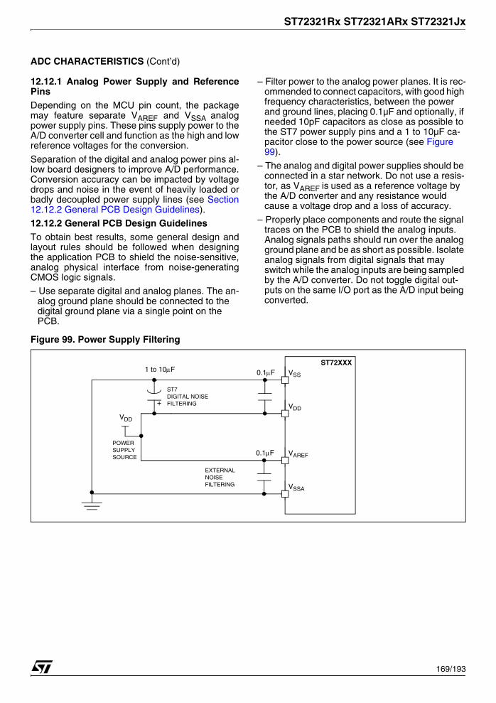
ST72321Rx ST72321ARx ST72321Jx
ADC CHARACTERISTICS (Cont’d)
12.12.1 Analog Power Supply and ReferencePinsDepending on the MCU pin count, the packagemay feature separate VAREF and VSSA analogpower supply pins. These pins supply power to theA/D converter cell and function as the high and lowreference voltages for the conversion.
Separation of the digital and analog power pins al-low board designers to improve A/D performance.Conversion accuracy can be impacted by voltagedrops and noise in the event of heavily loaded orbadly decoupled power supply lines (see Section12.12.2 General PCB Design Guidelines).
12.12.2 General PCB Design GuidelinesTo obtain best results, some general design andlayout rules should be followed when designingthe application PCB to shield the noise-sensitive,analog physical interface from noise-generatingCMOS logic signals.
– Use separate digital and analog planes. The an-alog ground plane should be connected to the digital ground plane via a single point on the PCB.
– Filter power to the analog power planes. It is rec-ommended to connect capacitors, with good high frequency characteristics, between the power and ground lines, placing 0.1µF and optionally, if needed 10pF capacitors as close as possible to the ST7 power supply pins and a 1 to 10µF ca-pacitor close to the power source (see Figure 99).
– The analog and digital power supplies should be connected in a star network. Do not use a resis-tor, as VAREF is used as a reference voltage by the A/D converter and any resistance would cause a voltage drop and a loss of accuracy.
– Properly place components and route the signal traces on the PCB to shield the analog inputs. Analog signals paths should run over the analog ground plane and be as short as possible. Isolate analog signals from digital signals that may switch while the analog inputs are being sampled by the A/D converter. Do not toggle digital out-puts on the same I/O port as the A/D input being converted.
Figure 99. Power Supply Filtering
VSS
VDD
VDD
ST72XXX
VAREF
VSSA
POWERSUPPLYSOURCE
ST7DIGITAL NOISEFILTERING
EXTERNALNOISEFILTERING
1 to 10μF 0.1μF
0.1μF
169/193
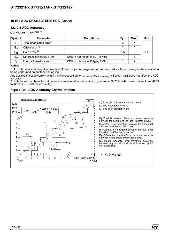
ST72321Rx ST72321ARx ST72321Jx
10-BIT ADC CHARACTERISTICS (Cont’d)
12.12.3 ADC AccuracyConditions: VDD=5V 1)
Notes:1. ADC Accuracy vs. Negative Injection Current: Injecting negative current may reduce the accuracy of the conversionbeing performed on another analog input.Any positive injection current within the limits specified for IINJ(PIN) and ΣIINJ(PIN) in Section 12.8 does not affect the ADCaccuracy.2. Data based on characterization results, monitored in production to guarantee 99.73% within ± max value from -40°Cto 125°C (± 3σ distribution limits).
Figure 100. ADC Accuracy Characteristics
Symbol Parameter Conditions Typ Max2) Unit
|ET| Total unadjusted error 1) 3 4
LSB
|EO| Offset error 1) 2 3
|EG| Gain Error 1) 0.5 3
|ED| Differential linearity error 1) CPU in run mode @ fADC 2 MHz. 1 2
|EL| Integral linearity error 1) CPU in run mode @ fADC 2 MHz. 1 2
EO
EG
1 LSBIDEAL
1LSBIDEAL
VAREF VSSA–
1024--------------------------------------------=
Vin (LSBIDEAL)
(1) Example of an actual transfer curve(2) The ideal transfer curve(3) End point correlation line
ET=Total Unadjusted Error: maximum deviationbetween the actual and the ideal transfer curves.EO=Offset Error: deviation between the first actualtransition and the first ideal one.EG=Gain Error: deviation between the last idealtransition and the last actual one.ED=Differential Linearity Error: maximum deviationbetween actual steps and the ideal one.EL=Integral Linearity Error: maximum deviationbetween any actual transition and the end pointcorrelation line.
Digital Result ADCDR
1023
1022
1021
5
4
3
2
1
0
7
6
1 2 3 4 5 6 7 1021 1022 1023 1024
(1)
(2)
ET
ED
EL
(3)
VAREFVSSA
170/193

ST72321Rx ST72321ARx ST72321Jx
13 PACKAGE CHARACTERISTICS
13.1 PACKAGE MECHANICAL DATA
Figure 101. 64-Pin Low Profile Quad Flat Package (14x14)
Figure 102. 64-Pin Low Profile Quad Flat Package (10 x10)
Dim.mm inches1)
Min Typ Max Min Typ Max
A 1.60 0.0630
A1 0.05 0.15 0.0020 0.0059
A2 1.35 1.40 1.45 0.0531 0.0551 0.0571
b 0.30 0.37 0.45 0.0118 0.0146 0.0177
c 0.09 0.20 0.0035 0.0079
D 16.00 0.6299
D1 14.00 0.5512
E 16.00 0.6299
E1 14.00 0.5512
e 0.80 0.0315
θ 0° 3.5° 7° 0° 3.5° 7°
L 0.45 0.60 0.75 0.0177 0.0236 0.0295
L1 1.00 0.0394
Number of Pins
N 64Note 1. Values in inches are converted from mmand rounded to 4 decimal digits.
c
h
L
L1
e
b
A
A1
A2
EE1
D
D1
Dim.mm inches1)
Min Typ Max Min Typ Max
A 1.60 0.0630
A1 0.05 0.15 0.0020 0.0059
A2 1.35 1.40 1.45 0.0531 0.0551 0.0571
b 0.17 0.22 0.27 0.0067 0.0087 0.0106
c 0.09 0.20 0.0035 0.0079
D 12.00 0.4724
D1 10.00 0.3937
E 12.00 0.4724
E1 10.00 0.3937
e 0.50 0.0197
θ 0° 3.5° 7° 0° 3.5° 7°
L 0.45 0.60 0.75 0.0177 0.0236 0.0295
L1 1.00 0.0394
Number of Pins
N 64
Note 1. Values in inches are converted from mm and rounded to 4 decimal digits.
A
A2
A1
c
θ
L1
L
EE1
D
D1
e
b
171/193

ST72321Rx ST72321ARx ST72321Jx
PACKAGE MECHANICAL DATA (Cont’d)
Figure 103. 44-Pin Low Profile Quad Flat Package
Figure 104. 32-Pin Low Profile Quad Flat Package-
Dim.mm inches1)
Note 1. Values in inches are converted from mm and rounded to 4 decimal digits.
Min Typ Max Min Typ Max
A 1.60 0.0630
A1 0.05 0.15 0.0020 0.0059
A2 1.35 1.40 1.45 0.0531 0.0551 0.0571
b 0.30 0.37 0.45 0.0118 0.0146 0.0177
C 0.09 0.20 0.0035 0.0079
D 12.00 0.4724
D1 10.00 0.3937
E 12.00 0.4724
E1 10.00 0.3937
e 0.80 0.0315
θ 0° 3.5° 7° 0° 3.5° 7°
L 0.45 0.60 0.75 0.0177 0.0236 0.0295
L1 1.00 0.0394
Number of Pins
N 44
AA2
A1
b
e
L1L
h
c
EE1
DD1
Dim.mm inches1)
Note 1. Values in inches are converted from mm and rounded to 4 decimal digits.
Min Typ Max Min Typ Max
A 1.60 0.0630
A1 0.05 0.15 0.0020 0.0059
A2 1.35 1.40 1.45 0.0531 0.0551 0.0571
b 0.30 0.37 0.45 0.0118 0.0146 0.0177
C 0.09 0.20 0.0035 0.0079
D 9.00 0.3543
D1 7.00 0.2756
E 9.00 0.3543
E1 7.00 0.2756
e 0.80 0.0315
θ 0° 3.5° 7° 0° 3.5° 7°
L 0.45 0.60 0.75 0.0177 0.0236 0.0295
L1 1.00 0.0394
Number of Pins
N 32
h
c
L
L1
b
e
A1
A2
A
EE1
D
D1
172/193

ST72321Rx ST72321ARx ST72321Jx
13.2 THERMAL CHARACTERISTICS
Notes:1. The maximum chip-junction temperature is based on technology characteristics.2. The maximum power dissipation is obtained from the formula PD = (TJ -TA) / RthJA. The power dissipation of an application can be defined by the user with the formula: PD=PINT+PPORT where PINT isthe chip internal power (IDDxVDD) and PPORT is the port power dissipation depending on the ports used in the applica-tion.
Symbol Ratings Value Unit
RthJA
Package thermal resistance (junction to ambient)LQFP64 14x14LQFP64 10x10LQFP44 10x10
475052
°C/W
PD Power dissipation 1) 500 mW
TJmax Maximum junction temperature 2) 150 °C
173/193

ST72321Rx ST72321ARx ST72321Jx
13.3 SOLDERING AND GLUEABILITY INFORMATION
Refer to JEDEC specification JSTD020D for a de-scription of the recommended reflow oven profilefor these packages.
In order to meet environmental requirements, SToffers this device in different grades of ECO-PACK® packages, depending on their level of en-vironmental compliance. ECOPACK® specifica-
tions, grade definitions and product status areavailable at: www.st.com. ECOPACK® is an STtrademark.
Recommended glue for SMD plastic packagesdedicated to molding compound with silicone:■ Heraeus: PD945, PD955■ Loctite: 3615, 3298
174/193

ST72321Rx ST72321ARx ST72321Jx
14 ST72321 DEVICE CONFIGURATION AND ORDERING INFORMATIONEach device is available for production in user pro-grammable versions (FLASH) as well as in factorycoded versions (ROM/FASTROM).
ST72321 devices are ROM versions. ST72P321devices are Factory Advanced Service TechniqueROM (FASTROM) versions: they are factory-pro-grammed HDFlash devices. FLASH devices are
shipped to customers with a default content, whileROM/FASTROM factory coded parts contain thecode supplied by the customer. This implies thatFLASH devices have to be configured by the cus-tomer using the Option Bytes while the ROM/FAS-TROM devices are factory-configured.
14.1 FLASH OPTION BYTES
The option bytes allow the hardware configurationof the microcontroller to be selected. They have noaddress in the memory map and can be accessedonly in programming mode (for example using astandard ST7 programming tool). The default con-tent of the FLASH is fixed to FFh. To program theFLASH devices directly using ICP, FLASH devicesare shipped to customers with the internal RCclock source enabled. In masked ROM devices,the option bytes are fixed in hardware by the ROMcode (see option list).
OPTION BYTE 0OPT7= WDG HALT Watchdog and HALT modeThis option bit determines if a RESET is generatedwhen entering HALT mode while the Watchdog isactive.0: No Reset generation when entering Halt mode1: Reset generation when entering Halt mode
OPT6= WDG SW Hardware or software watchdog This option bit selects the watchdog type.0: Hardware (watchdog always enabled)1: Software (watchdog to be enabled by software)
OPT5 = Reserved, must be kept at default value.
OPT4:3= VD[1:0] Voltage detectionThese option bits enable the voltage detectionblock (LVD, and AVD) with a selected threshold forthe LVD and AVD (EVD+AVD).
Caution: If the medium or low thresholds are se-lected, the detection may occur outside the speci-fied operating voltage range. Below 3.8V, deviceoperation is not guaranteed. For details on theAVD and LVD threshold levels refer to section12.3.2 on page 141
OPT2 = Reserved, must be kept at default value.
OPT1= PKG0 Package selection bit 0This option bit isused with the PKG1 bit to selectthe package.
STATIC OPTION BYTE 07 0
STATIC OPTION BYTE 17 0
WDG
Res
erve
d VD
Res
erve
d
PK
G0
FM
P_R
PK
G1
RS
TC
OSCTYPE OSCRANGE
PLL
OF
F
HA
LT
SW 1 0 1 0 2 1 0
Default 1 1 1 0 0 1 1 1 1 1 1 0 1 1 1 1
Selected Low Voltage Detector VD1 VD0
LVD and AVD Off 1 1Lowest Threshold: (VDD~3V) 1 0Med. Threshold (VDD~3.5V) 0 1Highest Threshold (VDD~4V) 0 0
175/193

ST72321Rx ST72321ARx ST72321Jx
ST72321 DEVICE CONFIGURATION AND ORDERING INFORMATION (Cont’d)
OPT0= FMP_R Flash memory read-out protectionRead-out protection, when selected, provides aprotection against Program Memory content ex-traction and against write access to Flash memo-ry.
Erasing the option bytes when the FMP_R optionis selected causes the whole user memory to beerased first, and the device can be reprogrammed.Refer to Section 4.3.1 and the ST7 Flash Pro-gramming Reference Manual for more details.Note: Readout protection is not supported if LVDis enabled.0: Read-out protection enabled1: Read-out protection disabled
OPTION BYTE 1OPT7= PKG1 Package selection bit 1This option bit selects the package.
Note: On the chip, each I/O port has up to 8 pads.Pads that are not bonded to external pins areforced in input pull-up configuration after reset.The configuration of these pads must be kept atreset state to avoid added current consumption.
are in input floating configuration after reset. Referto Note 4 on page 13.
OPT6 = RSTC RESET clock cycle selectionThis option bit selects the number of CPU cyclesapplied during the RESET phase and when exitingHALT mode. For resonator oscillators, it is advisedto select 4096 due to the long crystal stabilizationtime.0: Reset phase with 4096 CPU cycles1: Reset phase with 256 CPU cycles
OPT5:4 = OSCTYPE[1:0] Oscillator TypeThese option bits select the ST7 main clocksource type.
OPT3:1 = OSCRANGE[2:0] Oscillator rangeWhen the resonator oscillator type is selected,these option bits select the resonator oscillatorcurrent source corresponding to the frequencyrange of the used resonator. Otherwise, these bitsare used to select the normal operating frequencyrange.
OPT0 = PLLOFF PLL activationThis option bit activates the PLL which allows mul-tiplication by two of the main input clock frequency.The PLL is guaranteed only with an input frequen-cy between 2 and 4MHz, for this reason the PLLmust not be used with the internal RC oscillator. 0: PLL x2 enabled1: PLL x2 disabledCAUTION: the PLL can be enabled only if the“OSC RANGE” (OPT3:1) bits are configured to “2~4MHz”. Otherwise, the device functionality isnot guaranteed.
Version Selected Package PKG 1 PKG 0
(A)R LQFP64 1 0
J LQFP44 0 0
Clock SourceOSCTYPE
1 0
Resonator Oscillator 0 0
Reserved 0 1
Internal RC Oscillator 1 0
External Source 1 1
Typ. Freq. RangeOSCRANGE
2 1 0
1~2MHz 0 0 0
2~4MHz 0 0 1
4~8MHz 0 1 0
8~16MHz 0 1 1
176/193

ST72321Rx ST72321ARx ST72321Jx
ST72321 DEVICE CONFIGURATION AND ORDERING INFORMATION (Cont’d)
14.2 DEVICE ORDERING INFORMATION AND TRANSFER OF CUSTOMER CODE
Customer code is made up of the ROM/FAS-TROM contents and the list of the selected options(if any). The ROM/FASTROM contents are to besent on diskette, or by electronic means, with theS19 hexadecimal file generated by the develop-ment tool. All unused bytes must be set to FFh.
The selected options are communicated toSTMicroelectronics using the correctly completedOPTION LIST appended.
Refer to application note AN1635 for informationon the counter listing returned by ST after codehas been transferred. The STMicroelectronicsSales Organization will be pleased to provide de-tailed information on contractual points.
Caution: The Readout Protection binary value isinverted between ROM and FLASH products. Theoption byte checksum will differ between ROM andFLASH.
177/193

ST72321Rx ST72321ARx ST72321Jx
Figure 105. Ordering information scheme
ST72 F 321 J 7 T 8
FamilyST7 microcontroller family
Memory typeF: FlashBlank : ROMP = FASTROM
Memory size6 = 32K7 = 48K9 = 60K
PackageT = LQFP
Example:
No. of pinsJ = 44 or 42AR = 64 (LQFP64 10x10 package)R = 64 (LQFP64 14x14 package)
Sub-family325
Temperature range3 = -40 to 125 °C6 = -40 °C to 85 °C
For a list of available options (e.g. memory size, package) and orderable part numbers or for further informationon any aspect of this device, please contact the ST Sales Office nearest to you.
178/193

ST72321Rx ST72321ARx ST72321Jx
ST723251 DEVICE CONFIGURATION AND ORDERING INFORMATION (Cont’d)
Figure 106. ROM Factory Coded Device Types
DEVICE PACKAGE VERSION XXX/
Code name (defined by STMicroelectronics)
3 = Standard -40 to +125 °C6= Standard -40 to +85 °C
T= Plastic Thin Quad Flat Pack
ST72321AR9, ST72321AR7, ST72321AR6,ST72321R9, ST72321R7, ST72321R6ST72321J9, ST72321J7
179/193

ST72321Rx ST72321ARx ST72321Jx
ST72321 DEVICE CONFIGURATION AND ORDERING INFORMATION (Cont’d)
ST72321 MICROCONTROLLER OPTION LIST (last update Mar 2009)
Customer: . . . . . . . . . . . . . . . . . . . . . . . . . . . . . . . . . . . Address: . . . . . . . . . . . . . . . . . . . . . . . . . . . . . . . . . . . . . . . . . . . . . . . . . . . . . . . . . . . . . . . . . . . . . . Contact: . . . . . . . . . . . . . . . . . . . . . . . . . . . . . . . . . . . Phone No: . . . . . . . . . . . . . . . . . . . . . . . . . . . . . . . . . . . Reference/ROM Code* :. . . . . . . . . . . . . . . . . . . . . . . . *The ROM code name is assigned by STMicroelectronics. ROM code must be sent in .S19 format. .Hex extension cannot be processed.
Device Type/Memory Size/Package (check only one option): ----------------------|----------------|---------------------------------- ROM DEVICE: | 60K | 48K | 32K | ----------------------|----------------|---------------------------------- LQFP44 10x10: |[ ] ST72321J9 |[ ] ST72321J7 |[ ] see Note 1 | LQFP64 14x14: |[ ] ST72321R9 |[ ] ST72321R7 |[ ] ST72321R6 | LQFP64 10x10: |[ ] ST72321AR9 |[ ] ST72321AR7 |[ ] ST72321AR6 | ----------------------|----------------|---------------------------------- DIE FORM: | 60K | 48K | 32K | ----------------------|----------------|---------------------------------- 64-pin: | [ ] | [ ] | [ ] |
Conditioning (check only one option) : --------------------------------|----------------------------------------- Packaged Product | Die Product (dice tested at 25°C only) | --------------------------------|----------------------------------------- [ ] Tape & Reel [ ] Tray |[ ] Tape & Reel |[ ] Inked wafer |[ ] Sawn wafer on sticky foil
Version/Temp. Range (do not check for die product):Please refer to datasheet for specific sales conditions : Standard [ ] -40 to +85°C [ ] -40 to +125°C
Special Marking: [ ] No [ ] Yes "_ _ _ _ _ _ _ _ _ _ " (10 char. max) Authorized characters are letters, digits, '.', '-', '/' and spaces only.
Clock Source Selection: [ ] Resonator: [ ] LP: Low power resonator (1 to 2 MHz) [ ] MP: Medium power resonator (2 to 4 MHz) [ ] MS: Medium speed resonator (4 to 8 MHz) [ ] HS: High speed resonator (8 to 16 MHz) [ ] Internal RC (4) [ ] External Clock PLL (3) [ ] Disabled [ ] Enabled CSS (5) [ ] Disabled [ ] Enabled LVD Reset [ ] Disabled [ ] High threshold [ ] Med.threshold [ ] Low threshold
Reset Delay [ ] 256 Cycles [ ] 4096 Cycles Watchdog Selection: [ ] Software Activation [ ] Hardware Activation Watchdog reset on Halt [ ] Reset [ ] No reset Readout Protection(2): [ ] Disabled [ ] Enabled
Date . . . . . . . . . . . . . . . . . . . . . . . . Signature . . . . . . . . . . . . . . . . . . . . . . . .
Note 1 : Configure 44-pin/32K devices using separate ST72321B option list. Note 2 : Readout protection is not supported if LVD is enabled. Note 3 : PLL must not be enabled if internal RC Network or External Clock is selected. Note 4 : Internal RC can only be used if LVD is enabled. Note 5 : Device operation below 3.8V not guaranteed
180/193

ST72321Rx ST72321ARx ST72321Jx
DEVICE CONFIGURATION AND ORDERING INFORMATION (Cont’d)
14.3 DEVELOPMENT TOOLS
Development tools for the ST7 microcontrollers in-clude a complete range of hardware systems andsoftware tools from STMicroelectronics and third-party tool suppliers. The range of tools includessolutions to help you evaluate microcontroller pe-ripherals, develop and debug your application, andprogram your microcontrollers.
14.3.1 Starter kitsST offers complete, affordable starter kits. Starterkits are complete, affordable hardware/softwaretool packages that include features and samplesto help you quickly start developing your applica-tion.
14.3.2 Development and debugging toolsApplication development for ST7 is supported byfully optimizing C Compilers and the ST7 Assem-bler-Linker toolchain, which are all seamlessly in-tegrated in the ST7 integrated development envi-ronments in order to facilitate the debugging andfine-tuning of your application. The Cosmic CCompiler is available in a free version that outputsup to 16KBytes of code.
The range of hardware tools includes full-featuredST7-EMU3 series emulators and the low-costRLink in-circuit debugger/programmer. Thesetools are supported by the ST7 Toolset from ST-Microelectronics, which includes the STVD7 inte-grated development environment (IDE) with high-level language debugger, editor, project managerand integrated programming interface.
14.3.3 Programming toolsDuring the development cycle, the ST7-EMU3 se-ries emulators and the RLink provide in-circuitprogramming capability for programming the Flashmicrocontroller on your application board.
ST also provides a low-cost dedicated in-circuitprogrammer, the ST7-STICK, as well as ST7Socket Boards which provide all the sockets re-quired for programming any of the devices in aspecific ST7 sub-family on a platform that can beused with any tool with in-circuit programming ca-pability for ST7.
For production programming of ST7 devices, ST’sthird-party tool partners also provide a completerange of gang and automated programming solu-tions, which are ready to integrate into your pro-duction environment.
Evaluation boardsThree different Evaluation boards are available:■ ST7232x-EVAL ST72F321/324/521 evaluation
board, with ICC connector for programmingcapability. Provides direct connection to ST7-DVP3 emulator. Supplied with daughter boards(core module) for ST72F321, ST72324 &ST72F521.
■ ST7MDT20-EVC/xx1 with CAB LQFP64 14x14socket
■ ST7MDT20-EVY/xx1 with Yamaichi LQFP6410x10 socket
Table 29. STMicroelectronics Development Tools
Note 1: Add suffix /EU, /UK, /US for the power supply of your region.
Supported Products
Emulation Programming
ST7 DVP3 Series ST7 EMU3 seriesICC Socket Board
Emulator Connection kit EmulatorActive Probe &
T.E.B.
ST72321AR, ST72F321AR
ST7MDT20-DVP3
ST7MDT20-T6A/DVP ST7MDT20M-
EMU3ST7MDT20M-TEB ST7SB20M/xx1
ST72321R, ST72F321R
ST7MDT20-T64/DVP
ST72321J, ST72F321J
ST7MDT20-T44/DVP
ST7MDT20J-EMU3
ST7MDT20J-TEB ST7SB20J/xx1
181/193

ST72321Rx ST72321ARx ST72321Jx
DEVICE CONFIGURATION AND ORDERING INFORMATION (Cont’d)
Table 30. Suggested List of Socket Types
14.3.4 Socket and Emulator AdapterInformationFor information on the type of socket that is sup-plied with the emulator, refer to the suggested listof sockets in Table 30.
Note: Before designing the board layout, it is rec-ommended to check the overall dimensions of thesocket as they may be greater than the dimen-sions of the device.
For footprint and other mechanical informationabout these sockets and adapters, refer to themanufacturer’s datasheet.
Related DocumentationAN 978: ST7 Visual Develop Software Key Debug-ging Features
AN 1938: ST7 Visual Develop for ST7 Cosmic Ctoolset users
AN 1940: ST7 Visual Develop for ST7 AssemblerLinker toolset users
Device Socket (supplied with ST7MDT20M-
EMU3) Emulator Adapter (supplied with
ST7MDT20M-EMU3)
LQFP64 14 x14 CAB 3303262 CAB 3303351
LQFP64 10 x10 YAMAICHI IC149-064-*75-*5 YAMAICHI ICP-064-6
LQFP44 10 X10 YAMAICHI IC149-044-*52-*5 YAMAICHI ICP-044-5
182/193

ST72321Rx ST72321ARx ST72321Jx
14.4 ST7 APPLICATION NOTES
Table 31. ST7 Application Notes
IDENTIFICATION DESCRIPTIONAPPLICATION EXAMPLESAN1658 SERIAL NUMBERING IMPLEMENTATIONAN1720 MANAGING THE READ-OUT PROTECTION IN FLASH MICROCONTROLLERSAN1755 A HIGH RESOLUTION/PRECISION THERMOMETER USING ST7 AND NE555AN1756 CHOOSING A DALI IMPLEMENTATION STRATEGY WITH ST7DALI
AN1812A HIGH PRECISION, LOW COST, SINGLE SUPPLY ADC FOR POSITIVE AND NEGATIVE IN-PUT VOLTAGES
EXAMPLE DRIVERSAN 969 SCI COMMUNICATION BETWEEN ST7 AND PCAN 970 SPI COMMUNICATION BETWEEN ST7 AND EEPROMAN 971 I²C COMMUNICATION BETWEEN ST7 AND M24CXX EEPROMAN 972 ST7 SOFTWARE SPI MASTER COMMUNICATIONAN 973 SCI SOFTWARE COMMUNICATION WITH A PC USING ST72251 16-BIT TIMERAN 974 REAL TIME CLOCK WITH ST7 TIMER OUTPUT COMPAREAN 976 DRIVING A BUZZER THROUGH ST7 TIMER PWM FUNCTIONAN 979 DRIVING AN ANALOG KEYBOARD WITH THE ST7 ADCAN 980 ST7 KEYPAD DECODING TECHNIQUES, IMPLEMENTING WAKE-UP ON KEYSTROKEAN1017 USING THE ST7 UNIVERSAL SERIAL BUS MICROCONTROLLERAN1041 USING ST7 PWM SIGNAL TO GENERATE ANALOG OUTPUT (SINUSOÏD)AN1042 ST7 ROUTINE FOR I²C SLAVE MODE MANAGEMENTAN1044 MULTIPLE INTERRUPT SOURCES MANAGEMENT FOR ST7 MCUSAN1045 ST7 S/W IMPLEMENTATION OF I²C BUS MASTERAN1046 UART EMULATION SOFTWAREAN1047 MANAGING RECEPTION ERRORS WITH THE ST7 SCI PERIPHERALSAN1048 ST7 SOFTWARE LCD DRIVERAN1078 PWM DUTY CYCLE SWITCH IMPLEMENTING TRUE 0% & 100% DUTY CYCLEAN1082 DESCRIPTION OF THE ST72141 MOTOR CONTROL PERIPHERALS REGISTERSAN1083 ST72141 BLDC MOTOR CONTROL SOFTWARE AND FLOWCHART EXAMPLEAN1105 ST7 PCAN PERIPHERAL DRIVERAN1129 PWM MANAGEMENT FOR BLDC MOTOR DRIVES USING THE ST72141
AN1130AN INTRODUCTION TO SENSORLESS BRUSHLESS DC MOTOR DRIVE APPLICATIONS WITH THE ST72141
AN1148 USING THE ST7263 FOR DESIGNING A USB MOUSEAN1149 HANDLING SUSPEND MODE ON A USB MOUSEAN1180 USING THE ST7263 KIT TO IMPLEMENT A USB GAME PADAN1276 BLDC MOTOR START ROUTINE FOR THE ST72141 MICROCONTROLLERAN1321 USING THE ST72141 MOTOR CONTROL MCU IN SENSOR MODEAN1325 USING THE ST7 USB LOW-SPEED FIRMWARE V4.XAN1445 EMULATED 16-BIT SLAVE SPIAN1475 DEVELOPING AN ST7265X MASS STORAGE APPLICATIONAN1504 STARTING A PWM SIGNAL DIRECTLY AT HIGH LEVEL USING THE ST7 16-BIT TIMERAN1602 16-BIT TIMING OPERATIONS USING ST7262 OR ST7263B ST7 USB MCUSAN1633 DEVICE FIRMWARE UPGRADE (DFU) IMPLEMENTATION IN ST7 NON-USB APPLICATIONSAN1712 GENERATING A HIGH RESOLUTION SINEWAVE USING ST7 PWMARTAN1713 SMBUS SLAVE DRIVER FOR ST7 I2C PERIPHERALSAN1753 SOFTWARE UART USING 12-BIT ART
183/193

ST72321Rx ST72321ARx ST72321Jx
AN1947 ST7MC PMAC SINE WAVE MOTOR CONTROL SOFTWARE LIBRARYGENERAL PURPOSEAN1476 LOW COST POWER SUPPLY FOR HOME APPLIANCESAN1526 ST7FLITE0 QUICK REFERENCE NOTEAN1709 EMC DESIGN FOR ST MICROCONTROLLERSAN1752 ST72324 QUICK REFERENCE NOTEPRODUCT EVALUATIONAN 910 PERFORMANCE BENCHMARKINGAN 990 ST7 BENEFITS VS INDUSTRY STANDARDAN1077 OVERVIEW OF ENHANCED CAN CONTROLLERS FOR ST7 AND ST9 MCUSAN1086 U435 CAN-DO SOLUTIONS FOR CAR MULTIPLEXINGAN1103 IMPROVED B-EMF DETECTION FOR LOW SPEED, LOW VOLTAGE WITH ST72141AN1150 BENCHMARK ST72 VS PC16AN1151 PERFORMANCE COMPARISON BETWEEN ST72254 & PC16F876AN1278 LIN (LOCAL INTERCONNECT NETWORK) SOLUTIONSPRODUCT MIGRATIONAN1131 MIGRATING APPLICATIONS FROM ST72511/311/214/124 TO ST72521/321/324AN1322 MIGRATING AN APPLICATION FROM ST7263 REV.B TO ST7263BAN1365 GUIDELINES FOR MIGRATING ST72C254 APPLICATIONS TO ST72F264AN1604 HOW TO USE ST7MDT1-TRAIN WITH ST72F264AN2200 GUIDELINES FOR MIGRATING ST7LITE1X APPLICATIONS TO ST7FLITE1XBPRODUCT OPTIMIZATIONAN 982 USING ST7 WITH CERAMIC RESONATORAN1014 HOW TO MINIMIZE THE ST7 POWER CONSUMPTIONAN1015 SOFTWARE TECHNIQUES FOR IMPROVING MICROCONTROLLER EMC PERFORMANCEAN1040 MONITORING THE VBUS SIGNAL FOR USB SELF-POWERED DEVICESAN1070 ST7 CHECKSUM SELF-CHECKING CAPABILITY AN1181 ELECTROSTATIC DISCHARGE SENSITIVE MEASUREMENTAN1324 CALIBRATING THE RC OSCILLATOR OF THE ST7FLITE0 MCU USING THE MAINSAN1502 EMULATED DATA EEPROM WITH ST7 HDFLASH MEMORYAN1529 EXTENDING THE CURRENT & VOLTAGE CAPABILITY ON THE ST7265 VDDF SUPPLY
AN1530ACCURATE TIMEBASE FOR LOW-COST ST7 APPLICATIONS WITH INTERNAL RC OSCILLA-TOR
AN1605 USING AN ACTIVE RC TO WAKEUP THE ST7LITE0 FROM POWER SAVING MODEAN1636 UNDERSTANDING AND MINIMIZING ADC CONVERSION ERRORSAN1828 PIR (PASSIVE INFRARED) DETECTOR USING THE ST7FLITE05/09/SUPERLITEAN1946 SENSORLESS BLDC MOTOR CONTROL AND BEMF SAMPLING METHODS WITH ST7MCAN1953 PFC FOR ST7MC STARTER KITAN1971 ST7LITE0 MICROCONTROLLED BALLASTPROGRAMMING AND TOOLSAN 978 ST7 VISUAL DEVELOP SOFTWARE KEY DEBUGGING FEATURESAN 983 KEY FEATURES OF THE COSMIC ST7 C-COMPILER PACKAGEAN 985 EXECUTING CODE IN ST7 RAMAN 986 USING THE INDIRECT ADDRESSING MODE WITH ST7AN 987 ST7 SERIAL TEST CONTROLLER PROGRAMMINGAN 988 STARTING WITH ST7 ASSEMBLY TOOL CHAINAN1039 ST7 MATH UTILITY ROUTINES
Table 31. ST7 Application Notes
IDENTIFICATION DESCRIPTION
184/193

ST72321Rx ST72321ARx ST72321Jx
AN1071 HALF DUPLEX USB-TO-SERIAL BRIDGE USING THE ST72611 USB MICROCONTROLLERAN1106 TRANSLATING ASSEMBLY CODE FROM HC05 TO ST7
AN1179PROGRAMMING ST7 FLASH MICROCONTROLLERS IN REMOTE ISP MODE (IN-SITU PRO-GRAMMING)
AN1446 USING THE ST72521 EMULATOR TO DEBUG AN ST72324 TARGET APPLICATIONAN1477 EMULATED DATA EEPROM WITH XFLASH MEMORYAN1527 DEVELOPING A USB SMARTCARD READER WITH ST7SCRAN1575 ON-BOARD PROGRAMMING METHODS FOR XFLASH AND HDFLASH ST7 MCUSAN1576 IN-APPLICATION PROGRAMMING (IAP) DRIVERS FOR ST7 HDFLASH OR XFLASH MCUSAN1577 DEVICE FIRMWARE UPGRADE (DFU) IMPLEMENTATION FOR ST7 USB APPLICATIONSAN1601 SOFTWARE IMPLEMENTATION FOR ST7DALI-EVALAN1603 USING THE ST7 USB DEVICE FIRMWARE UPGRADE DEVELOPMENT KIT (DFU-DK)AN1635 ST7 CUSTOMER ROM CODE RELEASE INFORMATIONAN1754 DATA LOGGING PROGRAM FOR TESTING ST7 APPLICATIONS VIA ICCAN1796 FIELD UPDATES FOR FLASH BASED ST7 APPLICATIONS USING A PC COMM PORTAN1900 HARDWARE IMPLEMENTATION FOR ST7DALI-EVALAN1904 ST7MC THREE-PHASE AC INDUCTION MOTOR CONTROL SOFTWARE LIBRARYAN1905 ST7MC THREE-PHASE BLDC MOTOR CONTROL SOFTWARE LIBRARYSYSTEM OPTIMIZATIONAN1711 SOFTWARE TECHNIQUES FOR COMPENSATING ST7 ADC ERRORSAN1827 IMPLEMENTATION OF SIGMA-DELTA ADC WITH ST7FLITE05/09AN2009 PWM MANAGEMENT FOR 3-PHASE BLDC MOTOR DRIVES USING THE ST7FMCAN2030 BACK EMF DETECTION DURING PWM ON TIME BY ST7MC
Table 31. ST7 Application Notes
IDENTIFICATION DESCRIPTION
185/193

ST72321Rx ST72321ARx ST72321Jx
15 KNOWN LIMITATIONS
15.1 ALL FLASH AND ROM DEVICES
15.1.1 External RC option The External RC clock source option described inprevious datasheet revisions is no longer support-ed and has been removed from this specification.
15.1.2 Safe Connection of OSC1/OSC2 PinsThe OSC1 and/or OSC2 pins must not be left un-connected otherwise the ST7 main oscillator maystart and, in this configuration, could generate anfOSC clock frequency in excess of the allowedmaximum (>16MHz.), putting the ST7 in an un-safe/undefined state. Refer to section 6.2 on page25.
15.1.3 Reset pin protection with LVD EnabledAs mentioned in note 2 below Figure 89 on page160, when the LVD is enabled, it is recommendednot to connect a pull-up resistor or capacitor. A10nF pull-down capacitor is required to filter noiseon the reset line.
15.1.4 Unexpected Reset FetchIf an interrupt request occurs while a “POP CC” in-struction is executed, the interrupt controller doesnot recognise the source of the interrupt and, bydefault, passes the RESET vector address to theCPU.
WorkaroundTo solve this issue, a “POP CC” instruction mustalways be preceded by a “SIM” instruction.
15.1.5 External interrupt missedTo avoid any risk if generating a parasitic interrupt,the edge detector is automatically disabled for oneclock cycle during an access to either DDR andOR. Any input signal edge during this period willnot be detected and will not generate an interrupt.
This case can typically occur if the application re-freshes the port configuration registers at intervalsduring runtime.
WorkaroundThe workaround is based on software checkingthe level on the interrupt pin before and after writ-ing to the PxOR or PxDDR registers. If there is alevel change (depending on the sensitivity pro-grammed for this pin) the interrupt routine is in-voked using the call instruction with three extraPUSH instructions before executing the interruptroutine (this is to make the call compatible with theIRET instruction at the end of the interrupt serviceroutine).
But detection of the level change does not makesure that edge occurs during the critical 1 cycle du-ration and the interrupt has been missed. This maylead to occurrence of same interrupt twice (onehardware and another with software call).
To avoid this, a semaphore is set to '1' beforechecking the level change. The semaphore ischanged to level '0' inside the interrupt routine.When a level change is detected, the semaphorestatus is checked and if it is '1' this means that thelast interrupt has been missed. In this case, the in-terrupt routine is invoked with the call instruction.
There is another possible case i.e. if writing toPxOR or PxDDR is done with global interrupts dis-abled (interrupt mask bit set). In this case, thesemaphore is changed to '1' when the levelchange is detected. Detecting a missed interrupt isdone after the global interrupts are enabled (inter-rupt mask bit reset) and by checking the status ofthe semaphore. If it is '1' this means that the lastinterrupt was missed and the interrupt routine is in-voked with the call instruction.
To implement the workaround, the following soft-ware sequence is to be followed for writing into thePxOR/PxDDR registers. The example is for forPort PF1 with falling edge interrupt sensitivity. Thesoftware sequence is given for both cases (globalinterrupt disabled/enabled).
Case 1: Writing to PxOR or PxDDR with Global In-terrupts Enabled:
LD A,#01
LD sema,A ; set the semaphore to '1'
LD A,PFDR
AND A,#02
LD X,A ; store the level before writing toPxOR/PxDDR
LD A,#$90
LD PFDDR,A ; Write to PFDDR
LD A,#$ff
LD PFOR,A ; Write to PFOR
LD A,PFDR
AND A,#02
LD Y,A ; store the level after writing toPxOR/PxDDR
LD A,X ; check for falling edge
cp A,#02
jrne OUT
186/193

ST72321Rx ST72321ARx ST72321Jx
TNZ Y
jrne OUT
LD A,sema ; check the semaphore status ifedge is detected
CP A,#01
jrne OUT
call call_routine; call the interrupt routine
OUT:LD A,#00
LD sema,A
.call_routine ; entry to call_routine
PUSH A
PUSH X
PUSH CC
.ext1_rt ; entry to interrupt routine
LD A,#00
LD sema,A
IRET
Case 2: Writing to PxOR or PxDDR with Global In-terrupts Disabled:SIM ; set the interrupt mask
LD A,PFDR
AND A,#$02
LD X,A ; store the level before writing toPxOR/PxDDR
LD A,#$90
LD PFDDR,A; Write into PFDDRLD A,#$ff
LD PFOR,A ; Write to PFOR
LD A,PFDR
AND A,#$02
LD Y,A ; store the level after writing to PxOR/PxDDR
LD A,X ; check for falling edge
cp A,#$02jrne OUT
TNZ Y
jrne OUT
LD A,#$01
LD sema,A ; set the semaphore to '1' if edge isdetected
RIM ; reset the interrupt maskLD A,sema ; check the semaphore status
CP A,#$01
jrne OUT
call call_routine; call the interrupt routine
RIM
OUT: RIMJP while_loop
.call_routine ; entry to call_routine
PUSH A
PUSH X
PUSH CC .ext1_rt ; entry to interrupt routine
LD A,#$00
LD sema,A
IRET
15.1.6 Clearing active interrupts outsideinterrupt routineWhen an active interrupt request occurs at thesame time as the related flag is being cleared, anunwanted reset may occur.
Note: clearing the related interrupt mask will notgenerate an unwanted reset
Concurrent interrupt contextThe symptom does not occur when the interruptsare handled normally, i.e.
when:
– The interrupt flag is cleared within its own inter-rupt routine
– The interrupt flag is cleared within any interrupt routine
– The interrupt flag is cleared in any part of the code while this interrupt is disabled
If these conditions are not met, the symptom canbe avoided by implementing the following se-quence:
Perform SIM and RIM operation before and afterresetting an active interrupt request.
Example:
SIM
reset interrupt flag
RIM
Nested interrupt context:The symptom does not occur when the interruptsare handled normally, i.e.
when:
– The interrupt flag is cleared within its own inter-rupt routine
187/193

ST72321Rx ST72321ARx ST72321Jx
– The interrupt flag is cleared within any interrupt routine with higher or identical priority level
– The interrupt flag is cleared in any part of the code while this interrupt is disabled
If these conditions are not met, the symptom canbe avoided by implementing the following se-quence:
PUSH CC
SIM
reset interrupt flag
POP CC
188/193

ST72321Rx ST72321ARx ST72321Jx
KNOWN LIMITATIONS (Cont’d)
15.1.7 SCI Wrong Break durationDescriptionA single break character is sent by setting and re-setting the SBK bit in the SCICR2 register. Insome cases, the break character may have a long-er duration than expected:
- 20 bits instead of 10 bits if M=0
- 22 bits instead of 11 bits if M=1.
In the same way, as long as the SBK bit is set,break characters are sent to the TDO pin. Thismay lead to generate one break more than expect-ed.
OccurrenceThe occurrence of the problem is random and pro-portional to the baudrate. With a transmit frequen-cy of 19200 baud (fCPU=8MHz and SCI-BRR=0xC9), the wrong break duration occurrenceis around 1%.
WorkaroundIf this wrong duration is not compliant with thecommunication protocol in the application, soft-ware can request that an Idle line be generatedbefore the break character. In this case, the breakduration is always correct assuming the applica-tion is not doing anything between the idle and thebreak. This can be ensured by temporarily disa-bling interrupts.
The exact sequence is:
- Disable interrupts
- Reset and Set TE (IDLE request)
- Set and Reset SBK (Break Request)
- Re-enable interrupts
15.1.8 16-bit Timer PWM ModeIn PWM mode, the first PWM pulse is missed afterwriting the value FFFCh in the OC1R register(OC1HR, OC1LR). It leads to either full or no PWMduring a period, depending on the OLVL1 andOLVL2 settings.
15.1.9 TIMD set simultaneously with OCinterrupt If the 16-bit timer is disabled at the same time theoutput compare event occurs then output compareflag gets locked and cannot be cleared before thetimer is enabled again.
Impact on the application
If output compare interrupt is enabled, then theoutput compare flag cannot be cleared in the timerinterrupt routine. Consequently the interrupt serv-ice routine is called repeatedly.
WorkaroundDisable the timer interrupt before disabling the tim-er. Again while enabling, first enable the timer thenthe timer interrupts.
Perform the following to disable the timer:
TACR1 or TBCR1 = 0x00h; // Disable the com-pare interrupt
TACSR | or TBCSR | = 0x40; // Disable the timer
Perform the following to enable the timer again:
TACSR & or TBCSR &= ~0x40; // Enable the tim-er
TACR1 or TBCR1 = 0x40; // Enable the compareinterrupt
15.1.10 I2C MultimasterIn multimaster configurations, if the ST7 I2C re-ceives a START condition from another I2C mas-ter after the START bit is set in the I2CCR registerand before the START condition is generated bythe ST7 I2C, it may ignore the START conditionfrom the other I2C master. In this case, the ST7master will receive a NACK from the other device.On reception of the NACK, ST7 can send a re-startand Slave address to re-initiate communication
15.2 ALL FLASH DEVICES
15.2.1 Internal RC Oscillator with LVDThe internal RC can only be used if LVD is ena-bled.
15.3 LIMITATIONS SPECIFIC TO REV Q ANDREV S FLASH DEVICES
15.3.1 ADC AccuracyThe improved ADC accuracy specifications givenin Section 12.12.3 do not apply to Rev Q and RevS devices. Their accuracy remains as specified inthe previous datasheet revision and summarizedin the table below.
Symbol Parameter Typ Max Unit
|ET|Total unadjusted error
4 6
LSB
|EO| Offset error 3 5
|EG| Gain Error 0.5 4.5
|ED|Differential linearity error
1.5 4.5
|EL|Integral linearity er-ror
1.5 4.5
189/193

ST72321Rx ST72321ARx ST72321Jx
To identify these parts, check the internal salestype on the box label or the trace code marking onthe package.
15.4 LIMITATIONS SPECIFIC TO ROMDEVICES
15.4.1 LVD OperationDepending on the operating conditions, especiallythe VDD ramp up speed and ambient temperature,in some cases the LVD may not start. When thisoccurs, the MCU may operate outside the guaran-teed functional area (see datasheet Figure 76)without being forced into reset state.
In this case, proper use of the watchdog maymake it possible to recover through a watchdog re-set and allow normal operations to resume.
Consequently, the LVD function is not guaranteedin the current silicon revision. For complete securi-ty, an external reset circuit must be added.
Rev Internal Salestype Trace Code
Rev Q72F321xxx$A2
72F321xxx$U2
813xxxQ
813xxxQ
Rev S72F321xxx$A8
72F321xxx$U8
813xxxS
813xxxS
Rev 9 (full spec)
72F321xxx$A3
72F321xxx$U3
813xxx9
813xxx9
190/193

ST72321Rx ST72321ARx ST72321Jx
15.4.2 LVD Startup behaviourWhen the LVD is enabled, the MCU reaches itsauthorized operating voltage from a reset state.However, in some devices, the reset state is re-leased when VDD is approximately between 0.8Vand 1.5V. As a consequence, the I/Os may togglewhen VDD is within this window.
This may be an issue especially for applicationswhere the MCU drives power components.
Figure 107. LVD Startup Behaviour
15.4.3 AVD not supported On some devices with a specific VDD ramp upspeed the AVD may not start. As a result it cannotgenerate interrupts when VDD rises and falls.
15.4.4 Internal RC oscillator operation Internal RC oscillator operation is not supported inROM devices.
15.4.5 External clock source with PLLExternal clock source is not supported with thePLL enabled.
15.4.6 Pull-up not present on PE2 Unlike ST72F321 Flash devices, ST72321 ROMdevices have no weak pull-up on port PE2.In LQFP44 ROM devices, the PE2 pad is not con-nected to an internal pull-up like other unbondedpads (See note 4 under Table 2, “Device Pin De-scription,” on page 10). It is recommended to con-figure it as output push pull to avoid added currentconsumption.
15.4.7 Read-out protection with LVDThe LVD is not supported if Readout protection isenabled.
15.4.8 Safe Connection of OSC1/OSC2 PinsThe OSC1 and/or OSC2 pins must not be left un-connected otherwise the ST7 main oscillator maystart and, in this configuration, could generate anfOSC clock frequency in excess of the allowedmaximum (>16MHz.), putting the ST7 in an un-safe/undefined state. Refer to section 6.2 on page25.
5V
1.5V
VIT+
0.8V
LVD RESET
V DD
Window
t
191/193

ST72321Rx ST72321ARx ST72321Jx
16 REVISION HISTORY
Table 32. Revision History
Date Revision Description of Changes
18-Oct-2004 1.10
Added “related documentation” section in specific chapters throughout document
Flash readout protection sentence added section 4.3.1 on page 18
I2C Chapter updated, (Section 10.7)
Vt POR max modified in section 12.4 on page 142
Added Figure 89 on page 160
Modified description of tw(RSTL)out in “Asynchronous RESET Pin” on page 159
Added Note on PE2 pin in Table 2, “Device Pin Description,” on page 10
Modified VAREF min in “10-BIT ADC CHARACTERISTICS” on page 167
Modified IINJ for PC6 in Section 12.8
Updated ADC accuracy data and notes in section 12.12.3 on page 170 and “KNOWN LIM-ITATIONS” on page 186
Added “Clearing active interrupts outside interrupt routine” on page 187
I2C multimaster bug added in Known Limitations, Section 15.1.10
Please read carefully the “KNOWN LIMITATIONS” on page 186
13-Mar-2009 2
Updated root part numbers and device summary table on coverpage.
Removed temperature ranges 1, 5, and 7.
Renamed all TQFP packages, LQFP.
Updated note 6 below Table 2, “Device Pin Description,” on page 10.
Updated data retention in “Features” and Section 12.6.2 FLASH Memory.
Updated Figure 50 “Output Compare Timing Diagram, fTIMER = fCPU/4” .
Updated Figure 94 “SPI Master Timing Diagram 1)” .
Added Section 10.8.3.3 “Changing the conversion channel” on page 129.
Modified “Absolute Maximum Ratings (Electrical Sensitivity)” on page 155.
Update Note 4 in Section 12.8 I/O PORT PIN CHARACTERISTICS “General Characteris-tics” .
Updated notes in Section 13.2 THERMAL CHARACTERISTICS.
Removed recommended wave soldering profile and recommended reflow soldering oven profile, and added ECOPACK text in “SOLDERING AND GLUEABILITY INFORMATION” on page 174 (Section 13.3).
Removed automotive temperature ranges from Section 12.3.1 General Operating Condi-tions, and from Figure 106 “ROM Factory Coded Device Types” and option list. Modified Section 14.2 “DEVICE ORDERING INFORMATION AND TRANSFER OF CUSTOMER CODE” on page 177: replace list or order codes by ordering scheme.
Added Section 15.1.5 External interrupt missed, and Section 15.2.1 Internal RC Oscillator with LVD inSection 15 KNOWN LIMITATIONS. Modified Section 15.1.9 “TIMD set simulta-neously with OC interrupt” on page 189.
192/193

ST72321Rx ST72321ARx ST72321Jx
Please Read Carefully:
Information in this document is provided solely in connection with ST products. STMicroelectronics NV and its subsidiaries (“ST”) reserve theright to make changes, corrections, modifications or improvements, to this document, and the products and services described herein at anytime, without notice.
All ST products are sold pursuant to ST’s terms and conditions of sale.
Purchasers are solely responsible for the choice, selection and use of the ST products and services described herein, and ST assumes noliability whatsoever relating to the choice, selection or use of the ST products and services described herein.
No license, express or implied, by estoppel or otherwise, to any intellectual property rights is granted under this document. If any part of thisdocument refers to any third party products or services it shall not be deemed a license grant by ST for the use of such third party productsor services, or any intellectual property contained therein or considered as a warranty covering the use in any manner whatsoever of suchthird party products or services or any intellectual property contained therein.
UNLESS OTHERWISE SET FORTH IN ST’S TERMS AND CONDITIONS OF SALE ST DISCLAIMS ANY EXPRESS OR IMPLIEDWARRANTY WITH RESPECT TO THE USE AND/OR SALE OF ST PRODUCTS INCLUDING WITHOUT LIMITATION IMPLIEDWARRANTIES OF MERCHANTABILITY, FITNESS FOR A PARTICULAR PURPOSE (AND THEIR EQUIVALENTS UNDER THE LAWSOF ANY JURISDICTION), OR INFRINGEMENT OF ANY PATENT, COPYRIGHT OR OTHER INTELLECTUAL PROPERTY RIGHT.
UNLESS EXPRESSLY APPROVED IN WRITING BY AN AUTHORIZED ST REPRESENTATIVE, ST PRODUCTS ARE NOTRECOMMENDED, AUTHORIZED OR WARRANTED FOR USE IN MILITARY, AIR CRAFT, SPACE, LIFE SAVING, OR LIFESUSTAINING APPLICATIONS, NOR IN PRODUCTS OR SYSTEMS WHERE FAILURE OR MALFUNCTION MAY RESULT INPERSONAL INJURY, DEATH, OR SEVERE PROPERTY OR ENVIRONMENTAL DAMAGE. ST PRODUCTS WHICH ARE NOTSPECIFIED AS "AUTOMOTIVE GRADE" MAY ONLY BE USED IN AUTOMOTIVE APPLICATIONS AT USER’S OWN RISK.
Resale of ST products with provisions different from the statements and/or technical features set forth in this document shall immediately voidany warranty granted by ST for the ST product or service described herein and shall not create or extend in any manner whatsoever, anyliability of ST.
ST and the ST logo are trademarks or registered trademarks of ST in various countries.
Information in this document supersedes and replaces all information previously supplied.
The ST logo is a registered trademark of STMicroelectronics. All other names are the property of their respective owners.
© 2009 STMicroelectronics - All rights reserved
STMicroelectronics group of companies
Australia - Belgium - Brazil - Canada - China - Czech Republic - Finland - France - Germany - Hong Kong - India - Israel - Italy - Japan - Malaysia - Malta - Morocco - Singapore - Spain - Sweden - Switzerland - United Kingdom - United States of America
www.st.com
193/193