610f compiled comments aug 2012 - ipc--association ... compiled comments august 2012 late comments...
TRANSCRIPT

IPC-A-610F Compiled Comments August 2012
LATE COMMENTS
Commenters name,
company Reference Recommendation Reason for Recommendation Committee Resolution
There are four tables in this comment list. Table 1 lists all action comments. Table 2 lists new and unresolved comments and comments resolved at the most recent meeting. Table 3 lists all comments requiring IPC or graphics committee action. Table 4 lists all closed comments. These comments and changes were to correct editorial errors that were missed in publication of Rev E or non-criteria items that have been identified during training or translations.
TABLE 1 – ACTION ITEMS Commenters name,
company Reference 0 Recommendation Reason for Recommendation Committee Resolution
IPC Staff 4.1.4 1 User suggestion that Figure 4-11 would provide better representation if there was a PCB in the picture.
Action for committee members to provide photo or drawing
IPC Staff Blen Talbot, L-3 Comm.
6.2.3.1 2 [IPC] D2,3 bullet “Overlap…” should inverse of the A2,3 bullet for multiple pieces of sleeving. [Talbot] Acceptable – Class 2,3: delete the last bullet
The statement “Multiple pieces of sleeving overlap each other by at least 3 cable diameters, or 13 mm [0.5 inch], whichever is larger.” Is not within the scope of the clause.
Sleeving placement/sleeving overlap are the same topic in this clause. First recommendation Accepted <Sep2011> New information added for shrink sleeving – need to be reviewed/added to 610.<Feb2012>
Timothy Bajuscik, Ansaldo STS USA
7.2.2.1 3 The standard specifies that adhesive should be 50% (L) and 25% (D), but it does not give any specifics for how much should be in contact with the mounting surface. It only states that “Adhesion to mounting surface is evident.” In the attached, I tried to illustrate the scenario. Why doesn’t the standard specify how much of the adhesive needs to be in contact with the mounting surface? This meets the intent but it doesn’t provide much mechanical support.
Suggested text from Joe Kane: Acceptable 1, 2, 3 On any unsleeved horizontally mounted component, the staking material adheres to the component body and the mounting surface and extends at least 25% up the component diameter (D), for at least 50% of the component length (L) Defect 1, 2, 3 On any unsleeved horizontally mounted component, the staking material does not adhere to the component body and the mounting surface or extend at least 25% up the component diameter (D), for at least 50% of the component length (L) Suggestion from Jennifer Day Acceptable Class 1,2,3 On an unsleeved horizontally mounted component the staking material adheres to the component at least 50% of its length (L) and 25% of its diameter (D) on one side.
Task group of Jennifer D, Joe K, Jack, and Tino will review further. Open for now <<FEB2012>> 8/7/12-Jennifer Day sent recommendation to Team.

2
Commenters name, company
Reference 0 Recommendation Reason for Recommendation Committee Resolution
The build-up of staking material does not exceed 50% of the component diameter and continuous adhesion fillet to the mounting surface and component shall be a minimum of 25% and approximately centered on the body of component.
David Nelson, Raytheon
7.3.5.8 4 Eliminate “Process Indicator Class 2 Add Class 2 to “Acceptable-Class 1”
Bring into agreement with -001, 6.1.6 Accepted<<FEB2012> Floyd B to make a figure for Defect condition. <FEB2012>
David Nelson, Raytheon
7.4.3 5 Figure 7-133 Remove or replace Doesn’t show any of the defect criteria clearly. No solder present (Class 1 and 2). Doesn’t show insufficient to clinch and sorry, don’t know how to do this.
Accepted w/modification Figure moved to Acceptable<<FEB2012> Floyd B to make a figure for Defect condition. <FEB2012>
David Nelson, Raytheon
7.4.3 6 Figure 7-132 Label examples with appropriate Class Specifics eliminate confusion. See 7-109 for example. REVISIT TO CLARIFY Staff resolution: Accepted <<FEB2012> but no changes in draft. Leader resolution: Reject, drawing is defining “L”
Shirley Leyva, EMT 7.5.2 7 Figure 7-147 jumper wire routing is in error. All 3 jumpers have sharp bends, not per Table 4-1, 2 X outside diameter bend radius for insulated wire. Single conductor wire for jumpers cannot have sharp or kinked bends, it creates fractures in the wire. Figure 7-148 is correct.
Remove Figure 7-147 as Target, it should be Defect. This is causing confusion with operators and customers.
Figure to be modified by Gregg Owens <FEB2012>
IPC Staff 7.5.6 8 A1.2.3 suggestion from beta class; 2nd bullet bring in SMT lap solder to land criteria.
Discussion about first bullet and related defect. Is it the wire length that has to be from edge of land to knee or the solder fillet? Is it ok to have 25% of lead end unsoldered and still meet the 75% soldered criteria?
ACTION: Debbie Wade, ART to develop suggested wording. <Sep2011>
Ray Cirimele, STI Electronics
8.3.2.9.1 9 Swap the locations on the page of Figure 8-44 and 8-45. Figure 8-44 has no point of reference to determine the size of the device. It may or may not be larger than a 1206. Figure 8-45 definitely exceeds the 2:1 Width to Height ratio. There is no error in the text of the document, but it would be better to have the condition figure next to the associated text.
IPC to move 844 and 845 together. Defect Condition moved down with no figure. Floyd B to submit defect figure.<FEB2012>
David Nelson, Raytheon
8.3.14 10 Figure 8-175 Add top view drawing showing thermal plane connection attributes (End joint width, Side overhang and End overhang)
Clarification Accepted; note added to table. IPC ACTION to add all dimensions to dwg Floyd Bergagnolli ACTION to submit drawing<FEB2012>

3
IPC Staff 8.6.1.5 11 T1,2,3 has criteria for lead and solder. A1,2,3 and D1,2,3 only has criteria for min lead length; no solder criteria
ACTION: Debbie Wade, ART to develop suggested wording. <Sep2011> Action completed 9/20/2011, recommendation put into draft for committee review.<Sep2011> Action item still open waiting for Debbie per committee. <Feb2012>
John De Leeuw, SubCom
9.2 12 Provide additional information for chip resistor top coating damage for components below 1206.
We have 0805 resistor with damage to the top adhesive coating that extends about .007" from the edge. There doesn't appear to be any exposed element. The criteria for chipout in the top surface define acceptable damage for 1206 and larger components. It says nothing about damage in resistors smaller than 1206. Does this mean no damage regardless of size is acceptable below that size? If so, why is this particular size the "threshold?" Is there some place else in the 610 criteria that indicates acceptability of this for Class 3?
Gregg Owens Kathy Johnston Joe Kane Floyd B. to wordsmith and submit figures <FEB2012>
IPC Staff 10.2.4 13 D1,2,3 wording is cumbersome and hard for users to understand. Can this be simplified?
ACTION: IPC staff to separate edge delamination and haloing criteria for next draft. <Sep2011> Comment to be submitted to 600 & 6012 Committee<FEB2012> Staff: Aug 2012—who has this action and what comment to be submitted? Aug 2012--No splitting yet because this is on the synergy list.
Anitha Sinkfield, Delphi Electronics & Safety
10.8.2 14 I would like to discuss incorporation of these images and possibly some of the wording into the next revision of 610. We have to address bubbles in coating with our customers frequently, and I believe some revision to that section may make the discussions clearer. Proposal at the end of these comments
Subcommittee Dan and Teresa , Linda W, John M and Bruce Hughes to review images and make recommendations. <FEB2012>
TABLE 2 – NEW & OPEN COMMENTS
Commenters name,
company Reference Recommendation Reason for Recommendation Committee Resolution
Ray Cirimele, STI Electronics
4.5.2 15 Table 4-1 Change the Cable Type of the 6th row down from “CATS Ethernet cable” to “CAT 5 Ethernet cable”
Typo
620B Committee 2/2012
6.3.2 16 Additional statement added to this section in the 620B on 2/27/2012.
620B Committee 2/2012
6.3.4 17 2/2012 – 620B changed PI Class 2 to a Defect for wire strands exceeding 1 wire diameter
IPC Staff 6.14.1 18 The new table added Feb 2012 meeting needs a text reference.

4
Commenters name, company
Reference Recommendation Reason for Recommendation Committee Resolution
Omar Karin Hernandez
7.2.4 new 19 Heat Stake on Flexible and Rigid PCBA Criteria and pictures added to the end of these comments.
Alexander Phillips-Guardado, Electronic Evolution Tech
7.3.3 20 Table 7-3, Figure 7-75, Figure 7-77. in accordance to Table 7-4 and Figure 7-85 Recommendation: It looks like the exception of Figure 7-85 in relation of Table 7-4 about the fillet convex contradicts Table 7-3 and Figure 7-77 about lead protrusion that requires the end of the lead to be discernible in the solder and define the absent of that as a defect even for class 1. Can you guys revise this criterion and if possible help me understand it better.
We are an electronic manufacturing service provider and this criteria present a challenge to understand and the need to process our product as rework plus improvement of PTH soldering process.
Raul Sanchez, Kimball Electronics
7.3.5 21 I didn't see any clear definition for PTH solder joint about voids criteria related to the joint itself.
After X section we observed some voids in the solder on the barrel. We met the fill criteria, but we do not know the exact criteria for this.
Neil Wolford, Logic PD
7.3.5.1 22 Reference Figure 7-90 in A1A2A3 and move D1D2D3 down so that it is not in line with Figure 7-90.
Already marked for 610F corrections.
Neil Wolford, Logic PD
7.5.6 23 Remove from chapter 7. Could be moved to section 8.6.1.2.
Picture appears to be showing a surface mount component. It is in the through hole jumper wire section.
Kris Troxel 8.3.1.2 24 Maybe this is better in Section 9 for component damage. Add a section to define damage to area array components. To include: “Defect: Component exhibiting physical damage before or after assembly, including any of the following: Cracked, broken, or delaminated substrate Cracked, broken, or scorched solder mask on the
substrate Cracked or broken epoxy overmold Discolored or contaminated metal heat slug Separation of the heat slug from the substrate
There is no current definition of a damaged BGA.
Kris Troxel 10.1 25 Add a definition of “dead” gold fingers.
Add that missing “dead” fingers are acceptable. Add Defect - Damage or defects on dead fingers that adversely affect insertion (for example, due to burred or lifted edges)\
No current definition for dead fingers or definition of acceptance criteria.

5
Commenters name, company
Reference Recommendation Reason for Recommendation Committee Resolution
Kris Troxel 10.1.1 new 26 Add new criteria Gold Fingers - Surface Damage to Fingers Defects: Largest dimension of a single defect (scratches,
pinholes, pits) or the aggregate sum of the largest dimensions of several defects on a finger is 0.4 mm (0.016 in) or greater.
More than five defects (scratches, pinholes, pits) on each side of the board, per set of fingers that plug into a connector.
Surface defects in the contact area that expose base metal.
Defects that project up from or out of the contact surface area. (The contact area is defined as shown in Figure 10-2 of 610E.)
IPC staff 8.3.2.9.1 27 Notes next to Figures 8-4 and 8-45 say to “move figure away from Defect.” Are they to be removed completely? If not, where are they to be moved to?
Debbie Wade, ART 8.6.15 28 Additional jumper criteria added to the draft for committee review.
Neil Wolford, Logic PD
10.2.1 29 Standardize wording between bullets 1 of A2A3 and D2D3 for crazing. One currently talks about noncommon conductors and the other internal conductors. Noncommon conductors would also include external conductors. I presume crazing would not be an issue for external conductors. Crazing bullet 3 seems to be missing some wording between ...and conductive pattern ????? or more than... Not sure what the change should be. Error existed in Rev D also.
Clarification for bullet 1 and complete requirement for bullet 3.
Kirk Van Dreel, Plexus
10.8 30 Proposed conformal coating criteria is added at the end of these comments

6
Commenters name, company
Reference Recommendation Reason for Recommendation Committee Resolution
Young Park, I-SAC 10.5.5.3 10.5.5.4
31 When you see figure 2, you will find out that the labeling is a little lifted from the surface because of a thick head of the screw under the label, making the labeling not so smooth. Is there any standard for a lifting of labeling due to a screw used for the item?
Frank Kriesch, Diehl Aerospace
8.3.3.6 32 It is required to state that the provision of the minimum dimensions have to work together. Minimum solder joint width must be determined at the minimum solder joint height
I'm with the opinion of Teresa Rowe that both aspect of minimum requirement have to work together, otherwise you could have insufficient solder joints, but being acceptable according to IPC-A-610 aspects.
Omar Karin Hernandez
8.x new 33 Add criteria for SMT Compress Component – Soldering Criteria and pictures added to the end of these comments.
Mark Sorensen, ONYX (provided by Tino Gonzalez)
8.3.4.8 34 Add criteria for tilt & raise Target - Class 1,2,3 Component is perpendicular and base is parallel to
board. Clearance between base of component and board
surface/land is equal to solder thickness. Acceptable - Class 1,2,3 Component tilt does not violate minimum electrical
clearance. Process Indicator - Class 2,3 Component tilt / raise does not violate form fit and
function for component application.. Defect - Class 1,2,3 Violates minimum electrical clearance. Component tilt / raise violate form fit and function for
component application.
Pictures provided but embedded in pdf file; need separate pictures

7
TABLE 3 – IPC AND GRAPHICS COMMITTEE ACTION Commenters name,
company Reference Recommendation Reason for Recommendation Committee Resolution
IPC Staff 4.5.4 35 Figures 4-56 and 4-57. Both are good pix but each have attributes for both Target and A1,2,3 conditions. No matter which order they are inserted it can be confusing. Recommend removing white space between Target and A1,2,3.and adding keys in both figs for all attributes and referencing the keys in the bullets as appropriate.
IPC Action
IPC Staff 6.1.3 36 Figure 6-11; add arrow pointing at circumferential crack. IPC Action Meeting Sep 2011 6.11.1 37 T1,2,3 bring in J001E Figure 5-13 IPC Staff 8.1.2 38 Figure 8-6, correct pix to show 25% height IPC Action IPC Staff 11.1.6 39 Modify Fig 11-16 bottom view to add insulation spacing
like top view. IPC Action
Meeting Feb 2012 4.5.4 40 Figure 4-56 IPC action to add keys to figures and bullets IPC Action
Meeting Feb 2012 4.5.4 41 Figure 4-57 IPC action to add keys to figures and bullets IPC Action
IPC staff 7.1.1.1 42 Correct Figure 7-3; C2 R0 R5 so a wrong component (Defect) is being shown.
IPC Action
IPC staff 7.1.1.2 43 Need to assure the correct pix with four views is used IPC Action IPC staff 7.3.2 44 IPC action modify top bend in middle view to match other
two components IPC Action
Meeting Feb 2012 8.1.2 45 610E Fig 8-6 IPC action to correct dwg to show 25% height
IPC Action
Meeting Feb 2012 8.3.11 46 Figure 8-152 IPC action to delete K from illustration<Feb2012>
IPC Action
Meeting Feb 2012 8.3.14 47 Figure 8-175 IPC action to add all dimensions to drawing <Feb2012>
IPC Action
Meeting Feb 2012 11.1.6 48 Figure 11-16 IPC action to modify bottom view to add insulation spacing like top view
IPC Action
Meeting Feb 2012 12 49 Figure 12-4 IPC action to rekey bottom right to f and make insulation damage more obvious
IPC Action

8
TABLE 4 – RESOLVED COMMENTS Commenters name,
company Reference Recommendation Reason for Recommendation Committee Resolution
IPC Staff 1.1 50 Table 1-1 add 6010 series and A-600 Added to Sep 2011 draft. Editorial – agree – J DAY IPC Staff 1.4.1.4.1 51 Title correction: Process Control Methodologies Added to Sep 2011 draft. Editorial – agree – J DAY IPC Staff 1.4.1.5 52 Combined Conditions; last sentence, The manufacturer is
responsible for identification of such conditions. Add words to clarify that this needs to involve customer/user that knows the end use environment. Add sentence to end of paragraph:
Mel Parrish provided clarification for comment to consider. J DAY. The customer/user will identify additional limitations of combined conditions where there is significant concern based upon end use environment and product performance requirements.
Accepted with modification <Sep2011>
IPC Staff 1.5.6 53 Leaching definition; delete. Leaching is a cause, not the defect. Reference to leaching was deleted from component damage and this definition isn’t needed now.
Accepted to delete <Sep2011>
Thomas Fick, Safari Ckts
1.9 54 However, when an item is refereed it should be at the magnification called out based on the items classification from Table 1-2.
I believe that the reason for allowing higher magnification is so the inspector doesn’t need to constantly change magnification levels as they scan an assembly. However, this means that mixed technology boards are penalized, since thru hole parts are inspected at higher magnification. Items that wouldn’t be defects at lower magnification now get classified as a defect.
The current revision states that “magnification may be used for the entire assembly.” This is not a requirement. Action: Debbie Wade, ART will provide explanation to the commenter. <Sep2011>
John Borneman, Delphi Electronics
3.1 55 REMOVE 3.1.1 THROUGH 3.1.4 AND SECTION 3.2. Leave brief intro and reference to Industry standards as shown below in section 3.1. Suppliers of ESD sensitive electronic assemblies should reference industry standards such as ANSI/ESD S20.20 and IEC 61340-5-1.
Delphi is finding that some of our customers understand the value of IPC 610, but do are confused when IPC standards seem to conflict with other more accepted Industry standards. IPC 610 (current rev) is globally known and recognized as the standard for “workmanship issues”. In the case of ESD control, IPC 610 should not attempt to re-create or compete with something that others (ESDA and IEC) are doing better.
Accepted with modification<<FEB2012>> Section was determined to be helpful. Sections will be retained but a statement emphasizing that this is only a general section. For full ESD information the user of the document is referred to ANSI ESD 20.20.
IPC Staff 4.1.4 56 User suggested addition of defect for burred hardware. Is there a definition in T-50? – J DAY The task group doesn’t feel that a definition is necessary.<Sep2011>
IPC Staff 4.1.4 57 Figure 4-11 key 1 Lock washer, sharp edge towards flat washer. The first words properly identify the item; the rest of the words are criteria and should be a bullet rather than in the key. Propose new A1,2,3 bullet: Sharp edges of lock washer, if present, are mounted towards the flat washer.
Slight modification made to the key under the figure to clarify it is not criteria, just what is being shown. The first bullet next to this figure adequately defines the requirement. <Sep2011>
William Novak, Honeywell AZ
4.1.4 58 D1,2,3 Flat washing missing should ref Fig 4-13. Draft references 4-13 & 4-15 <Sep2011>
Keith Walker, EEI Mfg Svcs
4.1.4.2 59 According to the definitions of overlapped & overwrapped wire, D1,2,3 second bullet should be overwrapped, not overlapped.
Criteria modified <Sep2011>

9
Commenters name, company
Reference Recommendation Reason for Recommendation Committee Resolution
Les Bogert, Bechtel Plant Machinery Inc.
4.1.4.3 (new)
60 Proposed addition; 4.1.4.3 Hardware Installation – Threaded Fasteners – Other Threaded Items In addition to threaded fasteners used for installation of an item onto an assembly, there are other types of threaded items that may be used on individual parts within an assembly. These may require tightening to a specified torque value, or standard industry practice, to preclude loosening or part damage. Such items include, but are not limited to, connector coupling nuts, connector strain relief clamps/potting/molding boots, etc., fuse holder mounting nuts, and any other similar threaded items. Where torque values are not specified, follow standard industry practices. However, some of these threaded items may be made of plastic or other material that can be damaged if excessive torque is applied during assembly; and for these items, it may be necessary to tighten the item to a specified torque value. Acceptable – Class 1, 2, 3 Threaded items are tight. Torque value, if specified, is within limits. No evidence of damage resulting from over-tightening of the threaded item. Defect – Class 1, 2, 3 Threaded items are not tight. Torque value, if specified, is not within limits. Evidence of damage resulting from over-tightening of the threaded item.
Insert figure 9-5 from IPC/WHMA-A-620, except delete the arrows. If the figure is available showing the top of the connector include it here. The intent is to show the connector strain relief installed on the connector body. Insert figure 9-14 AND 12-4 from IPC/WHMA-A-620, except doctor the figures so they only show the threaded portion of the connectors
action from Sep2011 meeting: Accepted with Modification. The title of the section was changed to Threaded Fasteners and Other Threaded Hardware. Also added damage criteria to 9.13<<FEB2012>>
Michael Booth, Teledyne
4.2 61 Please find attached an improvement form with supporting documents for IPC-a-610e-2010. I believe there is a conflict between the jackpost mounting in IPC-610 and the applicable mil stds.
Committee did not accept the proposal for multiple criteria for different MilSpec connectors. This criteria is written toward typical connector installatons. <Sept2011>
IPC Staff 4.3.2.1 62 Replace terms secondary and primary side with protrusion and insertion side as more applicable to pins that could be inserted from either side.
Accepted <Sep2010>
William Novak, Honeywell AZ
4.5 63 Retitle from “routing: to “Wire Bundle Routing” For consistency Accepted with modification <Sep2011>
IPC Staff 4.5.2 64 Table 4-1; discovered during training development. The rows “Coaxial cables” and “Coaxial Flexible Cable” are the same thing according to Note 3 but the bend radius requirements are different, 5X and 10X.
Resolved through table update <Sep2011>
Les Bogert, Bechtel Plant Machinery Inc.
4.5.2 65 Where did the value of 1 inch for fiber optic cable bend radius in Table 4-1 come from? Normally, we spec bend radius as a function of the cable diameter. Also, if you look at MIL-PRF-85045/13 and /15 for shipboard type fiber optic cables, they mandate X16 bend radius for long term application and Table 4-1 uses X15. Not sure if we need to fix anything as part of 610F.
I assume as part of synergy with 620, we will make the tables in both documents the same.
Withdrawn but recommended to 610F telecom task group<<FEB2012>>
IPC Staff 6.1.1.1 66 Adjust title to current terminology: Swaged Hardware –Terminal Base to Land – Pad Gap
Accepted <Sep2011>
IPC Staff 6.1.1.1 67 Separate the Acceptable criteria by class to align to the Accepted <Sep2011>

10
Commenters name, company
Reference Recommendation Reason for Recommendation Committee Resolution
defect criteria that is already different by class. Suggestion is in the draft.
IPC Staff 6.1.1.2 68 A1,2,3 add key references to Fig 6-2. Terminal is bent, but the top edge (1) does not extend
beyond the base (2).
Added to Sep 2011 draft. Editorial – agree – J DAY
IPC Staff 6.1.5 69 Table 6-1 isn’t referenced in the text. Suggestion: These solder acceptance criteria, summarized in Table 6-1, are applicable to flared flange and flat set swaged hardware.
Added to Sep 2011 draft. Editorial – agree – J DAY
IPC Staff 6.1.5 70 Table 6-1, Editorial, item C change “in” to “on” Added to Sep 2011 draft. Editorial – agree – J DAY IPC Staff 6.1.5 71 Defect 1,2,3 and Defect 3, delete bullets about splits. This
is the solder section; split criteria is in 6.1.3 Added to Sep 2011 draft. Editorial – agree – J DAY
IPC Staff 6.1.5 72 Table 6-1 item B isn’t referenced with acceptable or defect bullets. Suggestion added to draft.
Accepted <Sep2011>
IPC Staff 6.1.5 73 Table 6-1 Item D isn’t referenced with acceptable or defect bullets. Current bullets are too generic; there are separate criteria for flare set and flat set eyelets. Suggestion added to draft.
Accepted <Sep2011>
IPC Staff 6.2.3.1 74 The first two bullets in D2,3 are the same as the bullet in D1. Change D1 to D1,2,3.
Accepted with modification <Sep2011>
Ray Cirimele, STI Electronics
6.3.2 Table 6-2 Change Note 1 from “No damaged strands for wires used at a potential of 6 kV or greater.” To “No damaged strands for wires used for high voltage.”
6 kV was what used to be the break point for it to be considered high voltage. The term ‘‘high voltage’’ will vary by design and application. We have to consider conductor spacing as well as voltage.
Not accepted Removing the requirement would possibly remove safety net for wires used above 6kV but not specified as High Voltage<<FEB2012>>
Blen Talbot, L-3 Comm.
6.6 75 Delete “(not shown)’ and reference Figure 6-64B. Clarification Agree – Editorial J DAY
Blen Talbot, L-3 Comm.
6.6 76 To the definition of “overwrap” add the text of Note 1 located in J-STD-001, below Table 5-3, “A wire that is wrapped more than 360º and remains in contact with the terminal post is considered an overwrap or spiral wrap and is not a defect.” To the definition of “overlap” add the text of Note 1 located in J-STD-001, below Table 5-3, “A wire that is wrapped more than 360º and crosses over itself, i.e., does not remain in contact with the terminal post is an overlap is defect.”
Needed for clarification and consistency between the documents. In 610 it doesn’t state that “overwrap” is not a Defect.
Committee did not want to expand the definition. The criteria for acceptability is covered in the bullets. <Sep2011>
Joseph Kane, BAE Systems
6.8.2 77 Change: Defect – Class 1,2 Solder is wetted less than 100% of the lead to terminal contact area when
the wrap is more than 90° and less than 180°. Defect – Class 1,2,3 Less than 75% fillet of the lead to terminal contact when the wrap is 180°
or more. Replace with the following: Defect – Class 1,2
Corrects inconsistent requirements and aligns with J-STD-001E Section 5.5. Note that with the existing 610E requirement, for Classes 1 and 2, if the wrap is 179°, then a fillet of 179° is required, while if the wrap is 180°, only 135° (75% of 180°) of wetted fillet is required. Also, if the wrap is more than 180°, then 610E is
Committee did not agree to this recommendation <Sep2011>

11
Commenters name, company
Reference Recommendation Reason for Recommendation Committee Resolution
Solder is wetted less than 90° along the circumference of the lead-to-terminal wrap.
Defect – Class 3 Solder is wetted less than 135° along the circumference of the lead-to-
terminal wrap.
much more stringent than J-1E for all three classes.
Joseph Kane, BAE Systems
6.9.4 78 Change: Defect – Class 1,2,3 Less than 100% fillet of the lead to terminal contact
when the wrap is less than 180° (not shown). Less than 75% fillet of the lead to terminal contact
when the wrap is 180° or more (not shown). Replace with the following: Defect – Class 1,2,3 Solder is wetted less than 90° along the circumference
of the lead-to-terminal wrap.
Simplifies requirements and aligns with J-STD-001E Section 5.5. As 610E is now, 179° of wrap requires more wetted fillet than 180° or more of wrap.
Committee did not agree to this recommendation <Sep2011>
IPC Staff 6.11.2 79 D1,2 editorial: Depression of solder between the terminal and the wrap of the wire…
There isn’t any “post” on pierced/perforated. Added to Sep 2011 draft.
Editorial – Agree J DAY
Joseph Kane, BAE Systems
6.11.2 80 Change: Defect – Class 1,2,3 Less than 100% fillet of the lead to terminal contact
when the wrap is less than 180°. Less than 75% fillet of the lead to terminal contact
when the wrap is 180° or more. Replace with the following: Defect – Class 1,2,3 Solder is wetted less than 90° along the circumference
of the lead-to-terminal wrap.
Simplifies requirements and aligns with J-STD-001E Section 5.5. As 610E is now, 179° of wrap requires more wetted fillet than 180° or more of wrap.
Committee did not agree to this recommendation <Sep2011>
Joseph Kane, BAE Systems
6.12.2 81 Change: Defect – Class 1,2,3 Less than 100% fillet of the lead to terminal contact
when the wrap is less than 180°. Less than 75% fillet of the lead to terminal contact
when the wrap is 180° or more. Replace with the following: Defect – Class 1,2 Solder is wetted less than 90° along the circumference
of the lead-to-terminal wrap. Defect – Class 3 Solder is wetted less than 135° along the
circumference of the lead-to-terminal wrap.
Simplifies requirements and aligns with J-STD-001E Section 5.5. As 610E is now, 179° of wrap requires more wetted fillet than 180° or more of wrap.
Committee did not agree to this recommendation <Sep2011>
Blen Talbot, L-3 Comm.
6.13.2 82 Figure 6-119; Delete the figure of a coax termination on the right side of the picture.
It’s not a cup terminal Accepted to delete the figure <Sep2011>
IPC Staff 7.1.1 83 Wrong term: Criteria are given for only the actual mounting or placement of components or wires on electronic assemblies and to standoff spacers.
Added to Sep 2011 draft. Editorial – Agree J DAY
IPC Staff 7.1.2.2 84 Intro; two places change to correct term: 14 usually cannot Common term is clearance (C). Added to Sep 2011 Editorial – Agree J DAY

12
Commenters name, company
Reference Recommendation Reason for Recommendation Committee Resolution
meet the maximum clearance requirements of a straight-legged vertical - radial leaded component, see 7.1.6. Maximum clearance between component and board surface
draft.
IPC Staff 7.1.2.2 85 A1P2D3 align to J001: Lead bends less than 1 lead diameter or thickness but
not less than 0.8 mm [0.031 in] away from body seal.
Added to Sep 2011 draft. Editorial – Agree J DAY
IPC Staff 7.2.1 86 T1,2,3 delete last bullet (min elect clearance). There is a defect bullet and normally MEC issues are only covered in defect or change to common terminology: Spacing between land and Uninsulated component
body exceeds does not violate minimum electrical clearance.
Search on “does not violate” shows sometimes under Target, a little more often under Acceptable. These should standardize; recommend under Acceptable.
Accepted to delete this bullet from Target <Sep2011>
IPC Staff 7.2.2.1 87 Last bullet is repeat of last bullet in N1P2D3; delete from this location
Added to Sep 2011 draft. Editorial – Agree J DAY
IPC Staff 7.2.3 88 Comment from beta class: Not always wires; sometimes metal straps. Suggest adding a bullet that the attaching wire/strap meets establish securing criteria.
Criteria modified <Sep2011>
IPC Staff 7.3.3 89 Intro sentence: change should not to shall not and delete electrical clearance; there’s already a defect bullet.
Added to Sep 2011 draft. Editorial – Agree J DAY
IPC Staff 7.3.4 90 Intro; editorial: Leads greater than 1.3 mm (.050 inch) should not be bent nor formed for mounting purposes. Is this referring to thick leads that should not be bent or short leads that should not be bent? Needs clarification
This is talking about thickness of lead and lead length - need clarification - verified with Mel P. Recommend changing to “Leads with thickness greater than. J.DAY
Criteria modified <Sep2011>
IPC Staff 7.3.5 91 A1P2,3 Delete last bullet; fillet lift acceptable in 5.2.11 Accepted <Sep2011> Ted Labowski, Microboard Processing Inc.
7.3.5 92 The current requirement is 75% vertical solder fill regardless of soldering process (intrusive) or lead length (leads shorter than the board thickness). When performing intrusive soldering with a component whose lead is shorter than the thickness of the board, solder will not extend beyond the end of the lead.
My company is running into a problem with trying to intrusive solder a combination SMT/through hole connector. Specifically, the through hole ground pins in the connector only extend approximately 50% through the board thickness.
Committee did not agree to add this. <Sep2011>
IPC Staff 7.3.5.2 93 Also 7.3.5.3; Change name: 7.3.5.2 Primary Solder Destination Side - Lead to Barrel (B) Also 7.3.5.3 A1,2,3
Criteria are applicable to any soldering process (wave, intrusive, hand). The committee agreed to change the terms in 610E Table 7-4 but the section headers didn’t get changed. This aligns everything.
Accepted <Sep2011>
IPC Staff 7.3.5.4 94 Also 7.3.5.5; Change name: 7.3.5.3 Solder Source Side - Land Area Coverage (C)
Criteria are applicable to any soldering process (wave, intrusive, hand). The committee agreed to change the terms in 610E Table 7-4 but the section headers didn’t get changed. This aligns everything.
Accepted <Sep2011>
IPC Staff 7.3.5.4 95 Also 7.3.5.5; Change name: 7.3.5.3 Secondary Solder Source Side - Land Area Coverage (C) Also 7.3.5.5 T1,2,3 & A1,2,3
Criteria are applicable to any soldering process (wave, intrusive, hand). The committee agreed to change the terms in 610E Table 7-4 but the section headers didn’t get changed. This aligns everything.
Accepted <Sep2011>
IPC Staff 7.3.5.9 96 A1,2,3 second bullet editorial; add see 7.3.3 Added to Sep 2011 draft. Editorial – Agree J DAY
13
Commenters name, company
Reference Recommendation Reason for Recommendation Committee Resolution
IPC Staff 7.4.1 97 Fig 7-126 key 2 Clinch This is only pointing to a clinch; criteria shouldn’t be in keys under figures. Class 3 requirement is elsewhere. Added to Sep 2011 draft.
Editorial – Agree J DAY
Jan Kolsters, Phillips Lighting
7.4.5 98 Table 7-7; For class 1 and 2 the only rule is that fillet and wetting of lead and land should be at leads should be at least 270 degrees. Propsal for clinched leads on unsupported holes is to demand for a complete joint under the clinched part of the lead. For the rest the hole may be open.
The strength of a joint of clinched leads on unsupported holes comes mainly from the part under the clinhed part of the lead. As it is stated in the current document a joint of 270 degrees but not soldered under the clinched part would be ok. This would be, however a very weak joint!
Committee did not agree to add this. <Sep2011>
Kathy Palumbo, PA&LS, LLC
8.3 99 VIA in Pad for SOT23 style part with flat leads (similar to a flat lug lead) with no foot. (photo) They have a via in the pad that is affecting another lead. They also have vias in the pad on what looks like a D-PAK device in the Thermal connection. There is a note on Page 8-15 Note 6 that covers the VIA in Pad, but this note is only placed under the 1, 3, & 5 sided Chip Components. This note is also in the BGA section for voiding issues that it can cause. This note should be on the other tables so it applies to any device with a VIA in the pad, OR the solder fillet requirement for all the other lead shapes should be met regardless of the VIA in the pad. A VIA in a pad always scavenges solder from the required fillet area and the fillet size should be based on what you need for reliability for your end use environment.
Intent of the note was deleted from Tables 8-2, 8-3 & 8-11 and added as a general comment in Chapter 8 introduction. <Sep2011>
David Boyle, Northrop Grumman
8.3 100 1. Create a sub-category within Section 8 that sets LCCs, PBGAs, QFNs, and other self-centering devices apart from non-self-centering devices such as QFPs and CBGAs. 2. Establish zero (0) inches and/or percent as the permitted amount of side misalignment for Class III self-aligning devices.
IPC-610, Sect 8 covers SMD, including castellated, area array, and other bottom side terminated devices. The paste on which these parts are placed, when reflowed, creates a friction free surface that floats special parts like LCCs, LGAs, etc. So long as a series of process variables are within bounds, the surface tension forces at work during reflow will shift these parts into perfect alignment with the land. This shift is automatic, and tells the examiner that the solder paste has fully liquefied. It is a metric that speaks volumes about the part, the PWB, and the processes used to solder one to the other. The opposite is also true. Misalignment of these parts says that something is off – the solder paste did not reach liquidous long enough; there was too little solder paste printed to float the part; the part or land did not wet properly; and other unacceptable conditions. With the exception of PBGAs, IPC-610 today accepts LCCs, QFNs, and power FET type devices even if misaligned by 25% of the land width. For whatever reason misalignment was originally allowed, the effect is to allow improperly soldered devices on Class III, high reliability assemblies. If wetting is the most important aspect of soldering, perfect alignment of self-aligning parts is the proof that such wetting has occurred, and that other crucial aspects of the assembly process have taken place as well. Misaligned parts, by their very existence, mask at least one and possibly many undesirable characteristics. For these and other reasons, self-aligning parts should only be accepted when perfectly aligned with their lands.
The committee did not agree that separate criteria should be necessary for self-centering parts. Maximum overhang criteria is still applicable. <Sep2011>
IPC Staff 8.3.1 101 Into; editorial to add words: The widths of the component Added to Sep 2011 draft. I agree that this editorial

14
Commenters name, company
Reference Recommendation Reason for Recommendation Committee Resolution
termination and land width are (W) and (P) The widths of the component termination (W) and land width (P) respectively
Robert Ninokata, ZNYX Networks
9.3 102 Under what ruling would a ferrite bead in a 0805 case fall? Is it safe to assume it should be similar to the resistor ruling for damage as stated in 9.3 if there is no damage to the resistive element?
Component data sheet for this device is available.
ACTION: Floyd Bertagnolli, STM to research damage allowance for this type of component. <Sep2011> Action completed 10/1/2011: Q1. Is the body a solid block of ferrite with a center metal piece, connecting the two metal terminations, or a standard ferrite toroid within molded plastic body? A1. Our parts are made with the solid block of ferrite. A2. Our parts do have conductors running through them that connect to terminations. There is no comment for the document as this is a question. Floyd completed the actions item as above. Submitter will be notified of the answers.<<FEB2012>>
IPC Staff 8.3.2.6 103 A1,2; add for clarity: Minimum fillet height (F) exhibits wetting on the
vertical surface(s) of the component termination.
Added to Sep 2011 draft. Editorial – Agree J DAY
IPC Staff 8.3.12.4 104 correct bullets to align to table: A1,2,3 25% or less voiding of any ball in the x-ray
image area. D1,2,3 More than 25% voiding of any ball in the x-
ray image area.
Added to Sep 2011 draft. Editorial agree – J DAY
Peter Phillips, Honeywell Aerospace
10.2.4 105 Haloing of non-plated thru holes in polyamide PWBs is causing concern both at the PWB supplier and the PWB user. As you are aware, polyamide is a brittle glasslike material and not as forgiving as the FR-4, etc.
Sub-Committee Leo Lambert, Mel Parrish, Sharon Ventress and Bruce Hughes is reviewing. <Aug2011>
Not accepted on subcommittee recommendation.<<FEB2012>>
David Miles, TE SubCom
10.2.6 106 BOW My concern is the acceptability of an assembled board with Spherical Bow and how board mounting conditions apply. I have spoken with Leo Lambert (EPTAC) and he suggested that the criteria for 10.2.6 was intended for boards that are rack mounted on slides with a connection to a backplane. Thus the board is not constrained except for the connector edge. In our product we have an 8.25" x 7" rectangular board that is mounted onto an aluminum chassis and secured with 16 screws around the perimeter plus 2 additional in the middle. We have a batch of boards from our supplier with 0.040" to 0.050" of spherical bow in the middle w.r.t. the edges. The board does not sit flat on the chassis. Thus I believe it violates the Fit requirement (from Form, Fit, or Function). We must be inducing stress into the board when we torque the 18 screws. My concern is how to apply 10.2.6 to our specific circumstances and would like to see further criteria included that would clearly cover the differences between a board that is secured to a chassis versus one installed in a rack.
The committee feels that the statement in the existing note sufficiently covers these concerns: “It may be necessary to confirm through testing that bow and twist has not created stress that will result in solder connection fracture or component damage.” <Sep2011>
15
Commenters name, company
Reference Recommendation Reason for Recommendation Committee Resolution
IPC Staff 10.5 107 Paragraph about RFID is extraneous and has nothing to do with applied markings. RFID is covered in 10.5.6. This paragraph should be deleted from 10.5.
Accepted <Sep2011>
IPC Staff 10.6.2 108 D1,2,3 first bullet; references to 5.2.7.1 & 10.7.2.2 left over from Rev D. These notes were reviewed on 9/09 for Rev E. 5.2.7.1 is still correct but 10.8.2 should have been referenced. J DAY
Fixed <Sep2011>
Joseph Kane, BAE Systems
10.7.1 109 By Fig 10-109 change: Acceptable – Class 1,2 Defect – Class 3 Cracking of solder mask. Replace with the following: Acceptable – Class 1,2,3 Cracking of solder mask without loss of adhesion.
There is no clear reason why minor cracking as shown in Figure 10-109 should be a defect. In 10.7.2, for Class 3, flaking (which is cracking with loss of adhesion) is a process indicator only if it expose copper, and a defect only if it bridges conductors.
Accepted with modification <Sep2011>
Ray Cirimele, STI Electronics
10.8.3 Table 10-1 The coating thickness charts should be identical. The coating thickness tables in IPC-A-610, J-STD-001, and IPC-CC-830 are all different as a result of rounding and transcription errors
Not accepted. CC-830 is a material qualification document. J001 is a process document. The tables are not intended to be identical<<FEB2012>>
Mike Green, Lockheed Martin
10.8.4 new 110 Add all of the following: 10.8.4 Insulation Coating 10.8.4.1 Insulation Coating-General 10.8.4.2 Insulation Coating- Coverage All of the considerations used for conformal coating are applicable for insulation coating, except the surface where insulation coating is applied is generally not smooth enough for a uniform coating surface. Thin coating is not a target attribute. See 10.5.2.2 10.8.4.3Insulation Coating-Thickness Acceptable: Complete coverage with no exposed metal Defect: Exposed metal Note: The thickness requirements of 10.8.3 do not apply.
This material is used to provide insulation to an exposed conductor when conformal coating is insufficient to provide enough protection and encapsulation is too much. The uses of the material are to protect active electronics from conductive FOD of various types and to provide a partial moisture barrier. The material used is frequently a conformal coat like material with a thickener added. It may be painted on with a brush to a thickness of .020 minimum. Examples of using the material are on bolted solder lugs where the edge surface is not fully protected by conformal coating., component cases that are electively active, and wire terminations, particularly movable wires. It does not replace Conformal Coat. It establishes requirements for a different adhesive function. It also provides description for the new term, Insulation Coating. This process is used when conformal coat is insufficient and encapsulation is too much. We use a thicker adhesive and paint it on with a brush. Note: A change to IPC-T-50H is concomitant.
Accepted with minor modifications. <Sep2011>
16
Commenters name, company
Reference Recommendation Reason for Recommendation Committee Resolution
IPC Staff 11 111 Intro; delete paragraph and numbered items referring to discrete wire boards. Delete the sentence about Section 5; there is no soldering in this chapter.
Accepted <Sep20111>
IPC Staff 11.1.1 112 Reword T1,2,3 to clarify that 50% more turn means 50% more of one turn, not 50% more of the minimum number of turns in Table 11-1.
Criteria modified <Sep2011>
IPC Staff 11.1.9 113 Figure 11-21 key 1: 1. Initial contact corner Added to Sep 2011 draft. Editorial – Agree J DAY IPC Staff 11.1.9 114 D2,3 delete last bullet; this clause is insulation damage, not insulation
clearance. Recommend to move defect to section 11.1.5 J.DAY
Deleted <Sep2011>
IPC Staff 11.2 115 Delete clause about connector wire dress. It’s not relevant to this chapter and there isn’t any other appropriate place is this document. This and all other wired connector criteria is adequately covered in 620.
Accepted <Sep20111>
IPC Staff 12 116 T1,2,3 delete 3rd bullet. Redundant to last bullet that is worded better.
Added to Sep 2011 draft. Editorial – Agree J DAY
17
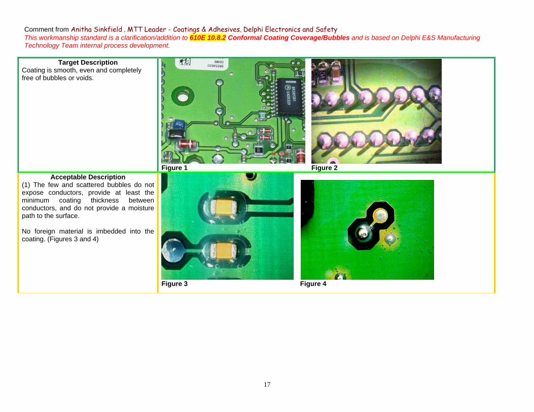
Comment from Anitha Sinkfield , MTT Leader - Coatings & Adhesives, Delphi Electronics and Safety This workmanship standard is a clarification/addition to 610E 10.8.2 Conformal Coating Coverage/Bubbles and is based on Delphi E&S Manufacturing Technology Team internal process development.
Target Description Coating is smooth, even and completely free of bubbles or voids.
Figure 1 Figure 2
Acceptable Description (1) The few and scattered bubbles do not expose conductors, provide at least the minimum coating thickness between conductors, and do not provide a moisture path to the surface. No foreign material is imbedded into the coating. (Figures 3 and 4)
Figure 3 Figure 4

18
(2) Bubble between the conductors does not provide conductive path between leads. There still exists at least one mil (0.001”) of coating over conductor (Figures 4 and 5)
Figure 5 Figure 6
(3) A continuous layer of coating seals the length of a lead and bubbles are the result of air being trapped behind the leads. (Figures 8 and 9)
Figure 7 Figure 8
Unacceptable Description (1) Bubbles provide a conductive path between leads and reduce coating thickness to less than 1 mil (0.001”) (Figures 10 and 11)
Figure 9
Bubbles on top of package are without consequence
Air void behind leads (acceptable)

19
(2) Surface void, or so-called “fish eye”, that expose the conductor, and leave a moisture path to the circuit trace. (Figures 10, 11 and 12)
Figure 10 Figure 11
Figure 12
Process Indicator Description (1) This depiction shows numerous, although shallow, bubbles that provide at least one mil (0.001”) of coating over the conductor trace. Although acceptable, this condition is difficult to evaluate, and should be corrected as soon as possible. Figure 13 (2) These numerous bubbles are only on the laminate, and do not form a continuous path between conductors. Although acceptable, this is indicative of improper machine set-up, and should be corrected as soon as possible
Figure 14
20
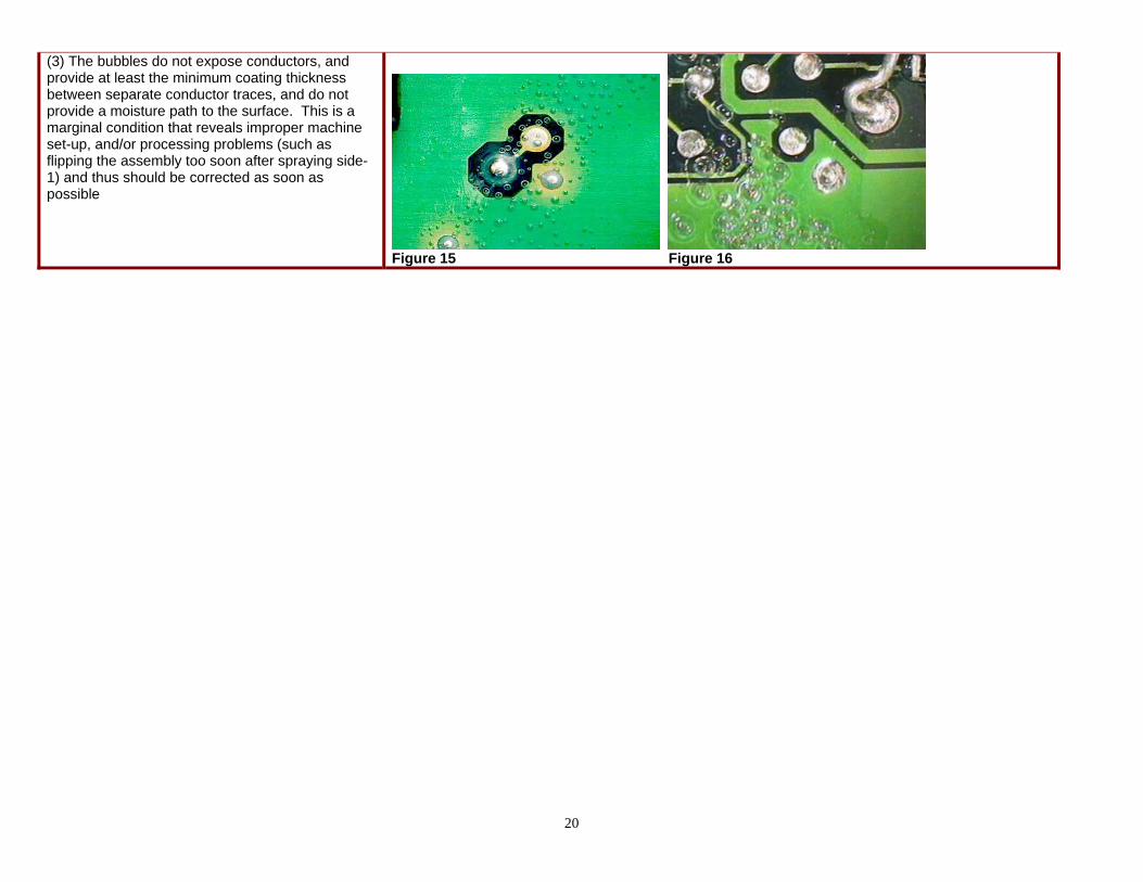
(3) The bubbles do not expose conductors, and provide at least the minimum coating thickness between separate conductor traces, and do not provide a moisture path to the surface. This is a marginal condition that reveals improper machine set-up, and/or processing problems (such as flipping the assembly too soon after spraying side-1) and thus should be corrected as soon as possible
Figure 15 Figure 16

21
Comment from Omar Karin Hernandez, Flextronics Guadalojara, submitted through Tino Gonzalez
SMT Compress Component – Soldering IDEAL Solder joint is equal to component termination width. Note: These criteria apply for square or circular PCBA pads. Acceptable – Class 1 & 2 Solder joint width (C) is minimum 50% of component termination width (W) or 50% land width
(P)
Acceptable – Class 3 Solder joint width (C) is minimum 75% of component termination width (W) or 75% land width
(P)

22
Defect – Class 1, 2 & 3 Solder joint is less than minimum acceptable
23
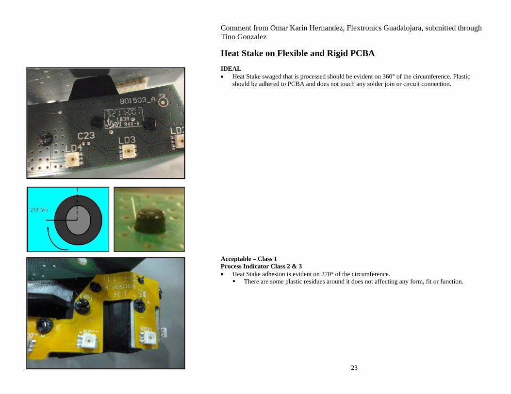
Comment from Omar Karin Hernandez, Flextronics Guadalojara, submitted through Tino Gonzalez
Heat Stake on Flexible and Rigid PCBA IDEAL Heat Stake swaged that is processed should be evident on 360° of the circumference. Plastic
should be adhered to PCBA and does not touch any solder join or circuit connection. Acceptable – Class 1 Process Indicator Class 2 & 3 Heat Stake adhesion is evident on 270° of the circumference.
There are some plastic residues around it does not affecting any form, fit or function.

24
Defect – Class 1, 2 & 3 Heat Stake adhesion is not evident at least than 270° of the circumference. Heat Stake Adhesion to the PCB is not evident. The Plastic interferes with the formation of a solder connection. The Plastic affects form, fit & function.

25
Comment from Kirk Van Dreel, Plexus 10.8 PCB Coverage Requirements
Target - Class 1,2,3 Evidence of complete coating coverage of all PCB surfaces not designated as keep out zones. All board edges have evidence of coverage and do not expose any inner or outer layers. Acceptable - Class 1,2 Defect - Class 3 Evidence of complete coating coverage of all exposed metal surfaces not designated as keep out
zones. Evidence of coating extending onto surrounding PCB perimeter of all coated metal surfaces at
least 1 width of the smallest land/conductor dimension.
Figure 10-x
Figure 10-x
Figure 10-x

26
Defect Class, 1,2,3 Evidence of exposed metal surfaces not designated as a keep out zone. Board edges have evidence of exposed inner or outer layers.
Figure 10-x
Figure 10-x
27
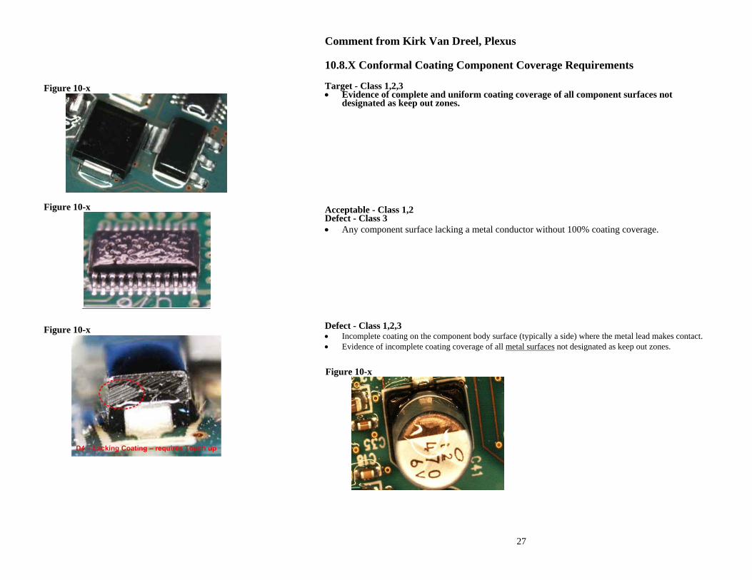
Comment from Kirk Van Dreel, Plexus 10.8.X Conformal Coating Component Coverage Requirements Target - Class 1,2,3 Evidence of complete and uniform coating coverage of all component surfaces not
designated as keep out zones. Acceptable - Class 1,2 Defect - Class 3 Any component surface lacking a metal conductor without 100% coating coverage. Defect - Class 1,2,3 Incomplete coating on the component body surface (typically a side) where the metal lead makes contact. Evidence of incomplete coating coverage of all metal surfaces not designated as keep out zones.
Figure 10-x
Figure 10-x
Figure 10-x
Figure 10-x
28
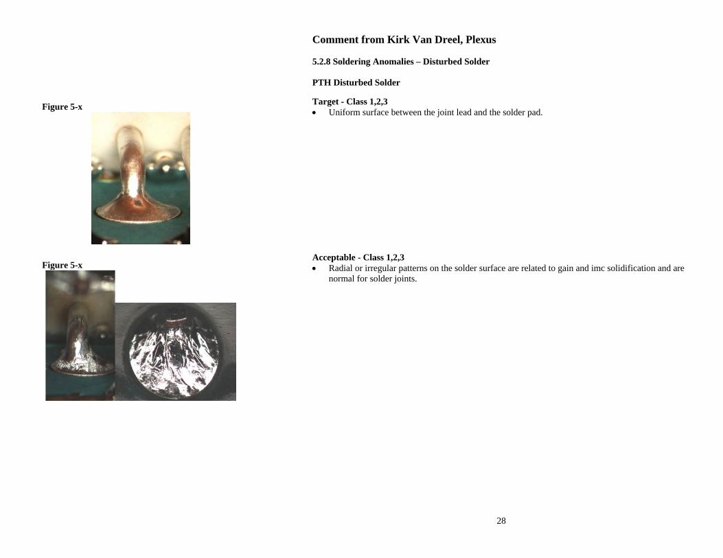
Comment from Kirk Van Dreel, Plexus 5.2.8 Soldering Anomalies – Disturbed Solder PTH Disturbed Solder Target - Class 1,2,3 Uniform surface between the joint lead and the solder pad. Acceptable - Class 1,2,3 Radial or irregular patterns on the solder surface are related to gain and imc solidification and are
normal for solder joints.
Figure 5-x
Figure 5-x

29
Defect - Class 1,2,3 Concentric solidification patterns on one or both sides of the joint.
Figure 5-x
Figure 5-x

30
5.2.12 Soldering Anomalies – [Lead Free] Hot Tear/Shrink Hole Target - Class 1,2,3 Uniform surface between the joint lead and the solder pad. Acceptable - Class 1,2,3 A hot tear or shrinkage void exists in the bulk solder and does not terminate on the land or lead. Defect - Class 1,2,3 The hot tear terminates at a lead or the PCB land pattern and the bottom of the hot tear cannot be
seen.
On the manufacturing floor it is difficult to distinguish between cracks and hot tears. Since a crack on a PTH starts at a feature (i.e. land or pad) this clarification will aid in this distinction between the two effects.
Figure 5-x
Figure 5-x
Figure 5-x