603xa service manual - matsolutions documents/agilent technologies/6035a/6035a...fail to execute...
TRANSCRIPT

SERVICE MANUAL
AUTORANGINGSYSTEM DC POWER SUPPLY
AGILENT MODELS 6030A, 6031A,6032A and 6035A
FOR INSTRUMENTS WITH SERIAL NUMBERS
Agilent Model 6030A; Serials US38320301 and above
Agilent Model 6031A; Serials US38310376 and above
Agilent Model 6032A; Serials US38321026 and above
Agilent Model 6035A; Serials US38320281 and above
For instruments with higher serial numbers, a change page may be included.
Agilent Part No. 5959-3344 Printed in USAMicrofiche Part No. 5959-3345 September, 2000

2
CERTIFICATION
Agilent Technologies certifies that this product met its published specifications at time of shipment from the factory. AgilentTechnologies further certifies that its calibration measurements are traceable to the United States National Bureau ofStandards, to the extent allowed by the Bureau's calibration facility, and to the calibration facilities of other InternationalStandards Organization members.
WARRANTYThis Agilent Technologies hardware product is warranted against defects in material and workmanship for a period of threeyears from date of delivery. Agilent Technologies software and firmware products, which are designated by AgilentTechnologies for use with a hardware product and when properly installed on that hardware product, are warranted not tofail to execute their programming instructions due to defects in material and workmanship for a period of 90 days from dateof delivery. During the warranty period Agilent Technologies will, at its option, either repair or replace products whichprove to be defective. Agilent Technologies does not warrant that the operation of the software, firmware, or hardware shallbe uninterrupted or error free.
For warranty service, with the exception of warranty options, this product must be returned to a service facility designatedby Agilent Technologies. Customer shall prepay shipping charges by (and shall pay all duty and taxes) for products returnedto Agilent Technologies for warranty service. Except for products returned to Customer from another country, AgilentTechnologies shall pay for return of products to Customer.
Warranty services outside the country of initial purchase are included in Agilent Technologies product price, only ifCustomer pays Agilent Technologies international prices (defined as destination local currency price, or U.S. or GenevaExport price).
If Agilent Technologies is unable, within a reasonable time to repair or replace any product to condition as warranted, theCustomer shall be entitled to a refund of the purchase price upon return of the product to Agilent.Technologies.
LIMITATION OF WARRANTYThe foregoing warranty shall not apply to defects resulting from improper or inadequate maintenance by the Customer,Customer-supplied software or interfacing, unauthorized modification or misuse, operation outside of the environmentalspecifications for the product, or improper site preparation and maintenance. NO OTHER WARRANTY IS EXPRESSEDOR IMPLIED. AGILENT TECHNOLOGIES. SPECIFICALLY DISCLAIMS THE IMPLIED WARRANTIES OFMERCHANTABILITY AND FITNESS FOR A PARTICULAR PURPOSE.
EXCLUSIVE REMEDIESTHE REMEDIES PROVIDED HEREIN ARE THE CUSTOMER'S SOLE AND EXCLUSIVE REMEDIES. AGILENTTECHNOLOGIES SHALL NOT BE LIABLE FOR ANY DIRECT, INDIRECT, SPECIAL, INCIDENTAL, ORCONSEQUENTIAL DAMAGES, WHETHER BASED ON CONTRACT, TORT, OR ANY OTHER LEGAL THEORY.
ASSISTANCEThe above statements apply only to the standard product warranty. Warranty options, extended support contracts, productmaintenance agreements and customer assistance agreements are also available. Contact your nearest AgilentTechnologies Sales and Service office for further information on Agilent Technologies' full line of Support Programs.

3
SAFETY SUMMARYThe following general safety precautions must be observed during all phases of operation, service and repair of thisinstrument. Failure to comply with these precautions or with specific warnings elsewhere in this manual violates safetystandards of design, manufacture, and intended use of the instrument. Agilent Technologies Inc. assumes no liability for thecustomer's failure to comply with these requirements.
BEFORE APPLYING POWER.Verify that the product is set to match the available line voltage and the correct fuse is installed.
GROUND THE INSTRUMENT.This product is a Safety Class 1 instrument (provided with a protective earth terminal). To minimize shock hazard, the instrument chassisand cabinet must be connected to an electrical ground. The instrument must be connected to the ac power supply mains through a three-conductor power cable, with the third wire firmly connected to an electrical ground (safety ground) at the power outlet. For instrumentsdesigned to be hard wired to the ac power lines (supply mains), connect the protective earth terminal to a protective conductor before anyother connection is made. Any interruption of the protective (grounding) conductor or disconnection of the protective earth terminal willcause a potential shock hazard that could result in personal injury. If the instrument is to be energized via an external autotransformer forvoltage reduction, be certain that the autotransformer common terminal is connected to the neutral (earth pole) of the ac power lines(supply mains).
INPUT POWER MUST BE SWITCH CONNECTED.For instruments without a built-in line switch, the input power lines must contain a switch or another adequate means for disconnectingthe instrument from the ac power lines (supply mains).
DO NOT OPERATE IN AN EXPLOSIVE ATMOSPHERE.Do not operate the instrument in the presence of flammable gases or fumes.
KEEP AWAY FROM LIVE CIRCUITS.Operating personnel must not remove instrument covers. Component replacement and internal adjustments must be made by qualifiedservice personnel. Do not replace components with power cable connected. Under certain conditions, dangerous voltages may exist evenwith the power cable removed. To avoid injuries, always disconnect power, discharge circuits and remove external voltage sources beforetouching components.
DO NOT SERVICE OR ADJUST ALONE.Do not attempt internal service or adjustment unless another person, capable of rendering first aid and resuscitation, is present.
DO NOT EXCEED INPUT RATINGS.This instrument may be equipped with a line filter to reduce electromagnetic interference and must be connected to a properly groundedreceptacle to minimize electric shock hazard. Operation at the line voltage or frequencies in excess of those stated on the data plate maycause leakage currents in excess of 5.0mA peak.
SAFETY SYMBOLS.Instruction manual symbol: the product will be marked with this symbol when it is necessary for the user to refer to theinstruction manual (refer to Table of Contents) .
Indicates hazardous voltages.
Indicate earth (ground) terminal.
The WARNING sign denotes a hazard. It calls attention to a procedure, practice, or the like, which, if not correctlyperformed or adhered to, could result in personal injury. Do not proceed beyond a WARNING sign until theindicated conditions are fully understood and met.
The CAUTION sign denotes a hazard. It calls attention to an operating procedure, or the like, which, if not correctlyperformed or adhered to, could result in damage to or destruction of part or all of the product. Do not proceed beyonda CAUTION sign until the indicated conditions are fully understood and met.
DO NOT SUBSTITUTE PARTS OR MODIFY INSTRUMENT.Because of the danger of introducing additional hazards, do not install substitute parts or perform any unauthorized modification to theinstrument. Return the instrument to an Agilent Technologies Sales and Service Office for service and repair to ensure that safety featuresare maintained.
Instruments which appear damaged or defective should be made inoperative and secured against unintended operation until they can berepaired by qualified service personnel.

4
Safety Symbol DefinitionsSymbol Description Symbol Description
Direct current Terminal for Line conductor on permanentlyinstalled equipment
Alternating current Caution, risk of electric shock
Both direct and alternating current Caution, hot surface
Three-phase alternating current Caution (refer to accompanying documents)
Earth (ground) terminal In position of a bi-stable push control
Protective earth (ground) terminal(Intended for connection to externalprotective conductor.)
Out position of a bi-stable push control
Frame or chassis terminal On (supply)
Terminal for Neutral conductor onpermanently installed equipment
Off (supply)
Terminal is at earth potential(Used for measurement and controlcircuits designed to be operated withone terminal at earth potential.)
Standby (supply)Units with this symbol are not completelydisconnected from ac mains when this switch isoff. To completely disconnect the unit from acmains, either disconnect the power cord or havea qualified electrician install an external switch.
Printing History
The edition and current revision of this manual are indicated below. Reprints of this manual containing minor correctionsand updates may have the same printing date. Revised editions are identified by a new printing date. A revised editionincorporates all new or corrected material since the previous printing date. Changes to the manual occurring betweenrevisions are covered by change sheets shipped with the manual. Also, if the serial number prefix of your power supply ishigher than those listed on the title page of this manual, then it may or may not include a change sheet. That is because eventhough the higher serial number prefix indicates a design change, the change may not affect the content of the manual.
Edition 1 June, 1991Edition2 September, 2000
© Copyright 1991, 2000 Agilent Technologies, Inc.
This document contains proprietary information protected by copyright. All rights are reserved. No part of this documentmay be photocopied, reproduced, or translated into another language without the prior consent of Agilent Technologies, Inc.The information contained in this document is subject to change without notice.

5
TABLE OF CONTENTSIntroduction ............................................................................................................................................................................ 9
Scope .................................................................................................................................................................................... 9Calibration and Verification ............................................................................................................................................. 9Troubleshooting................................................................................................................................................................ 9Principles of Operation ..................................................................................................................................................... 9Replaceable Parts.............................................................................................................................................................. 9Circuit Diagrams............................................................................................................................................................... 9
Safety Considerations ........................................................................................................................................................... 9Manual Revisions................................................................................................................................................................ 10Firmware Revisions ............................................................................................................................................................ 10
Calibration and Verification................................................................................................................................................ 11
Introduction......................................................................................................................................................................... 11Test Equipment Required ................................................................................................................................................... 11Operation Verification Tests............................................................................................................................................... 11Calibration Procedure ......................................................................................................................................................... 11
Initial Setup..................................................................................................................................................................... 14Voltage Monitor Zero Calibration .................................................................................................................................. 15Common Mode Calibration ............................................................................................................................................ 15Remote Readback Zero Calibration................................................................................................................................ 15Constant Voltage Full Scale Calibration......................................................................................................................... 17Voltage Monitor and Remote Readback Full Scale Calibration ..................................................................................... 17Constant Voltage Zero Calibration ................................................................................................................................. 18Current Monitor Zero Calibration................................................................................................................................... 18Constant Current Zero Calibration.................................................................................................................................. 18Current Monitor Full Scale Calibration .......................................................................................................................... 19Constant Current Full Scale Calibration ......................................................................................................................... 19Power Limit Calibration.................................................................................................................................................. 20Resistance Programming Full Scale Calibration............................................................................................................. 21
Performance Tests............................................................................................................................................................... 21Measurement Techniques ............................................................................................................................................... 21Constant Voltage (CV) Tests .......................................................................................................................................... 22Constant Current (CC) Tests........................................................................................................................................... 28
Initialization Procedure....................................................................................................................................................... 31
Troubleshooting .................................................................................................................................................................... 33
Introduction......................................................................................................................................................................... 33Initial Troubleshooting Procedures..................................................................................................................................... 33Electrostatic Protection....................................................................................................................................................... 34Repair and Replacement ..................................................................................................................................................... 34
A2 Control Board Removal ............................................................................................................................................ 35A4 FET Board Removal ................................................................................................................................................. 35A5 Diode Board Removal............................................................................................................................................... 36A8 GPIB Board Removal ............................................................................................................................................... 36A3 Front-Panel Board Removal...................................................................................................................................... 36A1 Main Board Removal ................................................................................................................................................ 36
Overall Troubleshooting Procedure.................................................................................................................................... 37GPIB Section Troubleshooting........................................................................................................................................... 39Primary Interface Troubleshooting ..................................................................................................................................... 40

6
Secondary Interface Troubleshooting ................................................................................................................................. 41Voltage and Current DAC............................................................................................................................................... 41Readback DAC Circuits.................................................................................................................................................. 43Readback Multiplexer (U20): ......................................................................................................................................... 43
Signature Analysis .............................................................................................................................................................. 45Primary SA ..................................................................................................................................................................... 45Front Panel SA................................................................................................................................................................ 45Secondary SA ................................................................................................................................................................. 46
Power Section Troubleshooting.......................................................................................................................................... 51Main Troubleshooting Setup........................................................................................................................................... 52Troubleshooting No-Output Failures .............................................................................................................................. 53Power Section Blocks ..................................................................................................................................................... 54Troubleshooting AC-Turn-On Circuits ........................................................................................................................... 57Troubleshooting DC-To-DC Converter .......................................................................................................................... 57Troubleshooting Bias Supplies ....................................................................................................................................... 58Troubleshooting Down Programmer............................................................................................................................... 61Troubleshooting CV Circuit ........................................................................................................................................... 61Troubleshooting CC Circuit............................................................................................................................................ 62Troubleshooting OVP Circuit ......................................................................................................................................... 62Troubleshooting PWM & Clock..................................................................................................................................... 63
Principles of Operation ........................................................................................................................................................ 65
Introduction......................................................................................................................................................................... 65GPIB Board ........................................................................................................................................................................ 65
Primary Microprocessor ................................................................................................................................................. 65Address Switches ........................................................................................................................................................... 65EEPROM........................................................................................................................................................................ 67Isolation .......................................................................................................................................................................... 67Secondary Microprocessor ............................................................................................................................................. 67Digital-to-Analog Converters.......................................................................................................................................... 67Analog Multiplexer......................................................................................................................................................... 67Status Inputs.................................................................................................................................................................... 67
Front Panel Board ............................................................................................................................................................... 68Address Latches and Decoders ....................................................................................................................................... 68Volts and Amps Output Ports and Displays.................................................................................................................... 68RPG and Latches ............................................................................................................................................................ 68Front-Panel Switches and Input Port............................................................................................................................... 68Mode Indicators .............................................................................................................................................................. 70OVP Adjust Control........................................................................................................................................................ 70Power Clear .................................................................................................................................................................... 70
Power Mesh and Control Board.......................................................................................................................................... 70Overview......................................................................................................................................................................... 70Power Mesh .................................................................................................................................................................... 71Control Board ................................................................................................................................................................. 73
Replaceable Parts.................................................................................................................................................................. 79
Introduction......................................................................................................................................................................... 79Ordering Information .......................................................................................................................................................... 80
Component Location and Circuit Diagrams .................................................................................................................... 101

7
l00 Vac Input Power Option 100 ....................................................................................................................................... 119
General Information.......................................................................................................................................................... 119Description.................................................................................................................................................................... 119Scope of Appendix A.................................................................................................................................................... 119Suggestions for Using Appendix A............................................................................................................................... 119Chapter 1 Manual Changes ........................................................................................................................................... 119Chapter 2 Manual Changes ........................................................................................................................................... 119Chapter 3 Manual Changes: .......................................................................................................................................... 123Chapter 4 Manual Changes: .......................................................................................................................................... 123Chapter 5 and 6 Manual Changes ................................................................................................................................. 123
Blank Front Panel Option 001........................................................................................................................................... 125
Introduction....................................................................................................................................................................... 125Troubleshooting............................................................................................................................................................ 125Chapter 2 Manual Changes: .......................................................................................................................................... 125Chapter 3 Manual Changes: .......................................................................................................................................... 126Chapter 5 and 6 Manual Changes: ................................................................................................................................ 126

9
1Introduction
Scope
This manual contains information for troubleshooting the Agilent 6030A, 6031A, 6032A, or 6035A 1000 W AutorangingPower Supply to the component level. Wherever applicable, the service instructions given in this manual refer to pertinentinformation provided in the Operation Manual (P/N 5959-3301). Both manuals cover Agilent Models6030A/31A/32A/35A; differences between models are described as required.
The following information is contained in this manual.
Calibration and VerificationContains calibration procedures for Agilent Models 6030A/31A/32A/35A. Also contains verification procedures that checkthe operation of the supplies to ensure they meet the specifications of Chapter 1 in the Operating Manual.
TroubleshootingContains troubleshooting procedures to isolate a malfunction to a defective component on the main circuit board or to adefective assembly (front panel, power transformer, or cable assembly). Board and assembly level removal and replacementprocedures are also given in this section.
Principles of OperationProvides block diagram level descriptions of the supply's circuits. The primary interface, secondary interface, and the powermesh and control circuits are described. These descriptions are intended as an aid in troubleshooting.
Replaceable PartsProvides a listing of replaceable parts for all electronic components and mechanical assemblies for Agilent Models6030A/31A/32A/35A.
Circuit DiagramsContains functional schematics and component location diagrams for all Agilent 6030A/31A/32A/35A circuits. The namesthat appear on the functional schematics also appear on the block diagrams in Chapter 2. Thus, the descriptions in Chapter 2can be correlated with both the block diagrams and the schematics.
Safety Considerations
This product is a Safety Class 1 instrument, which means that it is provided with a protective earth terminal. Refer to theSafety Summary page at the beginning of this manual for a summary of general safety information. Safety information forspecific procedures is located at appropriate places in the manual.
10
Manual Revisions
Agilent Technologies instruments are identified by a 10-digit serial number. The format is described as follows: first twoletters indicate the country of manufacture. The next four digits are a code that identify either the date of manufacture or of asignificant design change. The last four digits are a sequential number assigned to each instrument.
Item Description
US The first two letters indicates the country of manufacture, where US = USA.
3648 This is a code that identifies either the date of manufacture or the date of a significant design change.
0101 The last four digits are a unique number assigned to each power supply.
If the serial number prefix on your unit differs from that shown on the title page of this manual, a yellow Manual Changesheet may be supplied with the manual. It defines the differences between your unit and the unit described in this manual.The yellow change sheet may also contain information for correcting errors in the manual.
Note that because not all changes to the product require changes to the manual, there may be no update information requiredfor your version of the supply.
Older serial number formats used with these instruments had a two-part serial number, i.e. 2701A-00101. This manual alsoapplies to instruments with these older serial number formats. Refer to Appendix G for backdating information.
Firmware Revisions
The primary and secondary interface microcomputer chips inside of your supply are identified with labels that specify therevision of the supply's firmware. This manual applies to firmware revisions A.00.00, A.00.01, and A.00.02.
11
2Calibration and Verification
Introduction
This section provides test and calibration procedures. The operation-verification tests comprise a short procedure to verifythat the unit is performing properly, without testing all specified parameters. After troubleshooting and repair of a defectivepower supply you can usually verify proper operation with the turn-on checkout procedure in the Operating Manual. Repairsto the A1 main board, the A2 control board and the A8 GPIB board can involve circuits which, although functional, mayprevent the unit from performing within specified limits. So, after A1, A2 or A8 board repair, decide if recalibration andoperation verification tests are needed according to the faults you discover. Use the calibration procedure both to checkrepairs and for regular maintenance.
When verifying the performance of this instrument as described in this chapter, check only those specifications for which aperformance test procedure is included.
Test Equipment Required
Table 2-1 lists the equipment required to perform the tests of this section. You can separately identify the equipment forperformance tests, calibration and troubleshooting using the USE column of the table.
Operation Verification Tests
To assure that the unit is performing properly, without testing all specified parameters, first perform the turn-on checkoutprocedure in the Operating Manual. Then perform the following performance tests, in this section.
Voltage Programming And Readback AccuracyCurrent Programming And Readback AccuracyCV Load EffectCC Load Effect
Calibration Procedure
Calibrate the unit twice per year and when required during repair. The following calibration procedures should beperformed in the sequence given.
Note: Some of the calibration procedures for this instrument can be performed independently, and someprocedures must be performed together and/or in a prescribed order. If a procedure contains no referencesto other procedures, you may assume that it can be performed independently.
To return a serviced unit to specifications as quickly as possible with minimal calibration, the technicianneed only perform calibration procedures that affect the repaired circuit. Table 2-2 lists various powersupply circuits with calibration procedures that should be performed after those circuits are serviced.
If the GPIB board (A8) has been replaced, you must first initialize the board before you can calibrate theunit. Refer to Page 31.

12
Table 2-1. Test Equipment Required
TYPE REQUIRED CHARACTERISTICS USE RECOMMENDED MODELOscilloscope Sensitivity: 1 mV
Bandwidth: 20MHz & 100MHzInput: differential, 50 Ω & 10MΩ
P,T Agilent 54504A
RMS Voltmeter True rms, 10MHz bandwidthSensitivity: 1 mV Accuracy: 5%
P Agilent 3400B
Logic Pulser 4.5 to 5.5Vdc @ 35mA T Agilent 546AMultimeter Resolution: 100nV
Accuracy: 0.0035%, 6½ digitP,C,T Agilent 3458A
Signature Analyzer -- T Agilent 5004AGPIB Controller Full GPIB capabilities C,T,P HP Series, 200/300Current Probe No saturation at 100A
Bandwidth: 20Hz to 15MHzP Tek P6303 Probe
AM503 AmpTM500 Power Module
Electronic Load 6030A 200 V/5 A P,C 6050A & 60503A (4)60 V/17A 6050A & 60503A (4)
6031A 20 V/50 A 6050A & 60504A (2) 7 V/120 A 6050A & 60504A (2)6032A 60 V/17.5 A 6050A & 60504A (2)
20 V/50 A 6050A & 60504A (2)6035A 500 V/2 A
200 V/5 APower Resistor 250Ω 1% 1KW6050A & 60503A (4)
Current Shunt 0.1Ω/0.04%/15A/25W P,C Guildline 9230/150.01Ω/0.04%/100A/100W Guildline 9230/1000.001Ω/0.04%/300A/100W Guildline 9230/300
Power Resistors* 6030A 3.5Ω/40Ω 1% 1000 W (min.) P,C6031A 0.069Ω/0.04Ω 1% 1000W (min.)6032A 0.4Ω/3.5Ω 1% 1000W (min.)6035A 40Ω/250Ω 1% 1000W (min.)
Calibration and TestResistors
Value: 100Ω, 5%, 1W1Ω, 5%, ½W1KΩ, 5%, ¼W2KΩ, 0.01%, ¼W
C,T
TerminatingResistors (2)
Value: 50Ω ±5%, noninductive P
BlockingCapacitors (2)
Value: 0.01µF, 100Vdc P
Variable VoltageTransformer(autotransformer)
Adjustable from -13% to +6% of inputvoltage range, 4KVA minimum
P,C
Isolation Transformer 4KVA minimum TCommon-modeToroidal Core
≥3.7µH/turn2
≅23mm I.D.P Ferrox-Cube
500T600-3C8,Agilent 9170-0061
DC Power Supply Voltage range: 0-60VdcCurrent range: 0-3Adc
C,T Agilent 6024A
P = performance testing C = calibration adjustments T = troubleshooting* Not required if using electronic load.** Less accurate, and less expensive, current-monitor resistors can be used, but the accuracy to which current programmingand readback can be checked must be reduced accordingly.

13
Table 2-2. Guide to Recalibration After Repair
Printed CircuitBoard
Block Name Ref.Desig.
Perform These Procedures
A1 Main Board R3 Current Monitor Full Scale CalibrationConstant Current Full Scale Calibration
A1 Main Board T1, T2 Power Limit Calibration
A5 Diode Board CR4 Power Limit Calibration
A2 Control Board Constant Voltage Circuit All Voltage Monitor Zero Calibration(All Except Current Source) Common Mode Calibration
Remote Readback Zero CalibrationConstant Voltage Full Scale CalibrationVoltage Monitor and Remote Readback Full Scale CalibrationConstant Voltage Zero Calibration
A2 Control Board Constant Voltage Circuit All Resistance Programming Full Scale Calibration(Current Source)
A2 Control Board Constant Current Circuit All Current Monitor Zero CalibrationConstant Current Zero CalibrationCurrent Monitor Full Scale CalibrationConstant Current Full Scale Calibration
A2 Control Board Power Limit Comparator All Power Limit Calibration
A2 Control Board Bias Power Supplies All All Calibration procedures( + & -15V Supplies)
A8 GPIB Board Voltage Monitor Buffer All Voltage Monitor Zero CalibrationRemote Readback Zero CalibrationConstant Voltage Full Scale CalibrationVoltage Monitor and Remote Readback Full Scale CalibrationConstant Voltage Zero Calibration
A8 GPIB Board Analog Multiplexer All Remote Readback Zero CalibrationConstant Voltage Full Scale CalibrationVoltage Monitor and Remote Readback Full Scale CalibrationConstant Voltage Zero Calibration
A8 GPIB Board Readback DAC All Remote Readback Zero CalibrationConstant Voltage Full Scale CalibrationVoltage Monitor and Remote Readback Full Scale CalibrationConstant Voltage Zero Calibration
14
Table 2-2. Guide to Recalibration After Repair (continued)
Printed CircuitBoard
Block Name Ref.Desig.
Perform These Procedures
A8 GPIB Board Voltage DAC All Remote Readback Zero CalibrationConstant Voltage Full Scale CalibrationVoltage Monitor and Remote Readback Full Scale CalibrationConstant Voltage Zero Calibration
A8 GPIB Board Current DAC All Constant Current Zero CalibrationConstant Current Full Scale Calibration
A8 GPIB Board U5 Remote Readback Zero CalibrationConstant Voltage Full Scale CalibrationVoltage Monitor and Remote Readback Full Scale CalibrationConstant Voltage Zero CalibrationConstant Current Full Scale Calibration
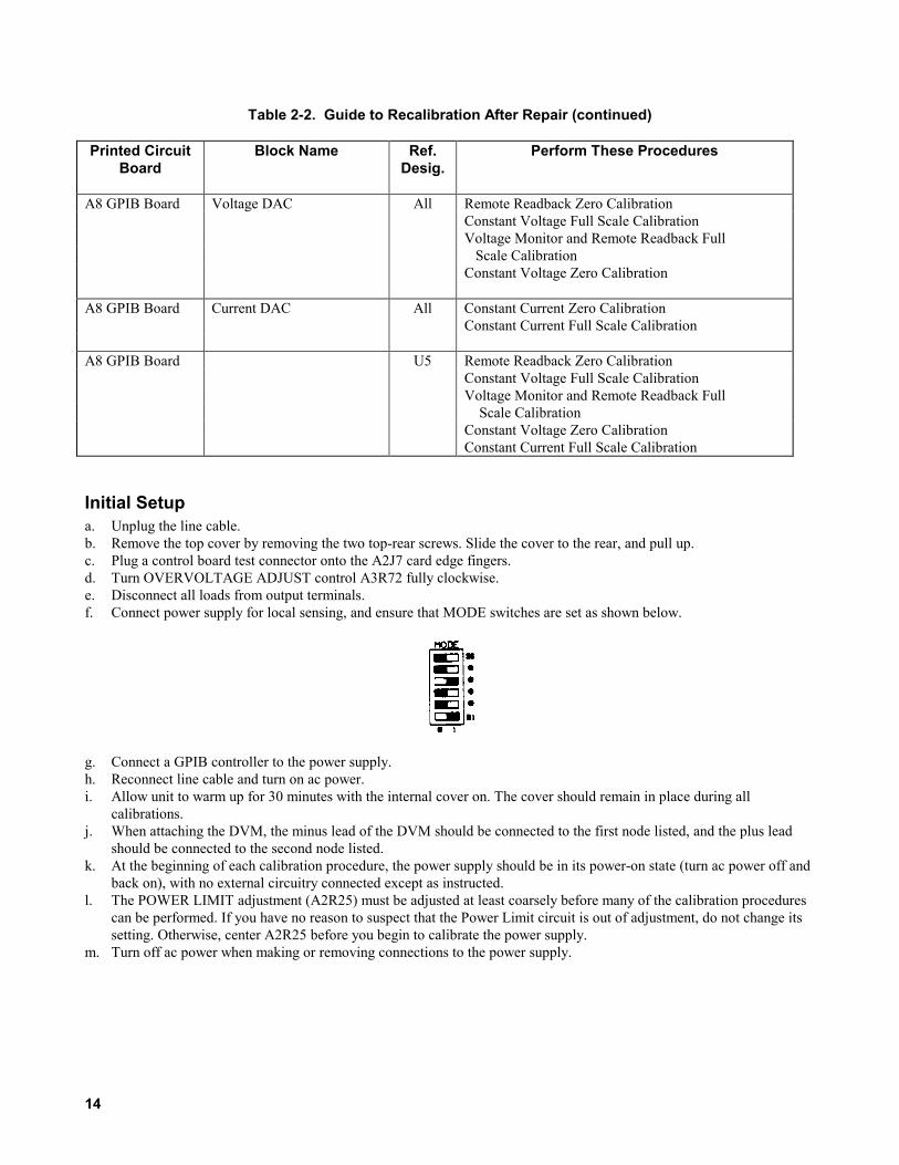
Initial Setupa. Unplug the line cable.b. Remove the top cover by removing the two top-rear screws. Slide the cover to the rear, and pull up.c. Plug a control board test connector onto the A2J7 card edge fingers.d. Turn OVERVOLTAGE ADJUST control A3R72 fully clockwise.e. Disconnect all loads from output terminals.f. Connect power supply for local sensing, and ensure that MODE switches are set as shown below.
g. Connect a GPIB controller to the power supply.h. Reconnect line cable and turn on ac power.i. Allow unit to warm up for 30 minutes with the internal cover on. The cover should remain in place during all
calibrations.j. When attaching the DVM, the minus lead of the DVM should be connected to the first node listed, and the plus lead
should be connected to the second node listed.k. At the beginning of each calibration procedure, the power supply should be in its power-on state (turn ac power off and
back on), with no external circuitry connected except as instructed.l. The POWER LIMIT adjustment (A2R25) must be adjusted at least coarsely before many of the calibration procedures
can be performed. If you have no reason to suspect that the Power Limit circuit is out of adjustment, do not change itssetting. Otherwise, center A2R25 before you begin to calibrate the power supply.
m. Turn off ac power when making or removing connections to the power supply.

15
Maintenance described herein is performed with power supplied to the instrument, and protective coversremoved. Such maintenance should be performed only by service trained personnel who are aware of the
hazards involved (for example, fire and electrical shock). Where maintenance can be performed without power applied, the power should be removed.
Voltage Monitor Zero Calibration
a. Send string "VSET 0; ISET 0; OUT OFF".b. Short power supply output terminals.c. Attach the DVM from M on the rear panel through a 1kΩ resistor to A2J7 pin 3 (V-MON buffered).d. Adjust A2R22 (V-MON ZERO) to 0V ±20µV. ( ± 40µV 6035A).
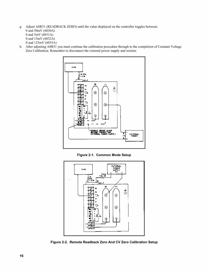
Common Mode Calibration
a. Send string ''VSET 0; ISET 0; OUT OFF".b. Short power supply sense terminals ( + S to - S) at rear panel.c. Attach the DVM from M on the rear panel through a 1kΩ resistor to A2J7 pin 3 (V-MON buffered).d. Take initial reading from DVM.e. Remove both local sensing straps from rear-panel terminal block, and connect a 1-volt external power supply with its +
lead to - S and its--lead to - Out. See Figure 2-1.f. Adjust A2R21 (CV LOAD REG) to Initial Reading ±20µV (6030A) ±80µV (6031A) ±20µV (6032A) ±40µV (6035A)g. Replace local sense straps after removing external power supply.
Note: Common mode calibration is not required for Agilent Model 6035A.
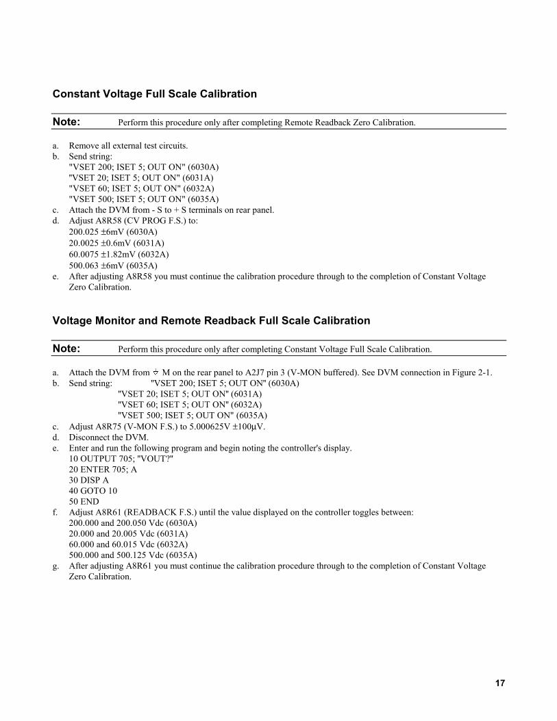
Remote Readback Zero Calibration
Note: This procedure and the following three procedures must be done as a set, without omitting any of the fourprocedures. Also, the following four procedures require that V-MON ZERO (A2R22) be adjusted withinspecifications. If it is not, perform the Voltage Monitor Zero Calibration before proceeding.
a. Connect an external supply to the power supply as shown in Figure 2-2.b. Send string "VSET 0; ISET 5; OUT ON''.c. Attach the DVM from M on the rear panel through a 1KΩ resistor to A2J7 pin 3 (V-MON buffered).d. Adjust A8R40 (CV PROG ZERO) to 625µV ± 30µV.e. Remove the DVM.f. Enter and run the following program and begin noting the controller's display: 10 OUTPUT 705; "VOUT'' 20 ENTER 705; A 30 DISP A 40 GOTO 10 50 END
16
g. Adjust A8R51 (READBACK ZERO) until the value displayed on the controller toggles between: 0 and 50mV (6030A) 0 and 5mV (6031A) 0 and 15mV (6032A) 0 and 125mV (6035A)h. After adjusting A8R51 you must continue the calibration procedure through to the completion of Constant Voltage
Zero Calibration. Remember to disconnect the external power supply and resistor.
Figure 2-1. Common Mode Setup
Figure 2-2. Remote Readback Zero And CV Zero Calibration Setup
17
Constant Voltage Full Scale Calibration
Note: Perform this procedure only after completing Remote Readback Zero Calibration.
a. Remove all external test circuits.b. Send string: "VSET 200; ISET 5; OUT ON" (6030A) ''VSET 20; ISET 5; OUT ON" (6031A) "VSET 60; ISET 5; OUT ON" (6032A) "VSET 500; ISET 5; OUT ON" (6035A)c. Attach the DVM from - S to + S terminals on rear panel.d. Adjust A8R58 (CV PROG F.S.) to: 200.025 ±6mV (6030A) 20.0025 ±0.6mV (6031A) 60.0075 ±1.82mV (6032A) 500.063 ±6mV (6035A)e. After adjusting A8R58 you must continue the calibration procedure through to the completion of Constant Voltage
Zero Calibration.
Voltage Monitor and Remote Readback Full Scale Calibration
Note: Perform this procedure only after completing Constant Voltage Full Scale Calibration.
a. Attach the DVM from M on the rear panel to A2J7 pin 3 (V-MON buffered). See DVM connection in Figure 2-1.b. Send string: ''VSET 200; ISET 5; OUT ON'' (6030A) ''VSET 20; ISET 5; OUT ON'' (6031A) ''VSET 60; ISET 5; OUT ON'' (6032A) ''VSET 500; ISET 5; OUT ON" (6035A)c. Adjust A8R75 (V-MON F.S.) to 5.000625V ±100µV.d. Disconnect the DVM.e. Enter and run the following program and begin noting the controller's display. 10 OUTPUT 705; ''VOUT?'' 20 ENTER 705; A 30 DISP A 40 GOTO 10 50 ENDf. Adjust A8R61 (READBACK F.S.) until the value displayed on the controller toggles between: 200.000 and 200.050 Vdc (6030A) 20.000 and 20.005 Vdc (6031A) 60.000 and 60.015 Vdc (6032A) 500.000 and 500.125 Vdc (6035A)g. After adjusting A8R61 you must continue the calibration procedure through to the completion of Constant Voltage
Zero Calibration.

18
Constant Voltage Zero Calibration
Note: Perform this procedure only after completing Voltage Monitor and Remote Readback Full ScaleCalibration.
a. Send string "VSET 0; ISET 5; OUT ON".b. Connect an external supply to the power supply as shown in Figure 2-2.c. Attach the DVM from - S to + S on the rear panel.d. Adjust A8R40 (CV PROG ZERO) to 0 ±120µV.
Current Monitor Zero Calibration
a. Send string "VSET 0; ISET 0; OUT OFF''.b. Connect a short across power supply output terminals.c. Attach the DVM from M to IM on the rear panel.d. Allow several minutes (3 or more) to ensure thermal settling.e. Adjust A2R8 (I-MON ZERO) to 0 ±100 µV.
Constant Current Zero Calibration
a. Connect the test setup shown in Figure 2-3.b. Send string ''VSET 5; ISET 0; OUT ON''.c. Allow several minutes (3 or more) to ensure thermal settling.d. Adjust A8R29 (CC PROG ZERO) to:
0V ±0.6mV (6030A, 6035A)0V ±8.0mV (6031A)0V ±1.7mV (6032A)
Figure 2-3. CC Zero Calibration Setup

19
Current Monitor Full Scale Calibration
Note: This procedure requires that I-MON ZERO (A2R8) be adjusted within specifications. If it is not, performthe Current Monitor Zero Calibration before proceeding.
a. Connect Rm current-monitoring shunt: (1milliohm, 6031A) (10 milliohm, 6030A, 6032A) (100 milliohm, 6035A) 0.05% or better across power supply output terminals.b. Send string: "VSET 5; ISET 17; OUT ON" (6030A) "VSET 5; ISET 120; OUT ON" (6031A) "VSET 5; ISET 50; OUT ON" (6032A) "VSET 5; ISET 5; OUT ON" (6035A)c. Attach DVM from M to IM on the rear panel. Use six-digit display on Agilent 3458A DVM.d. Take initial reading from DVM.e. Attach DVM across Rm. Allow several minutes (3 or more) to ensure thermal settling. This can be noted as a stable
reading on the DVM.f. Adjust A2R9 (I-MON F.S.) to:
0.034 * initial reading ±33.5µV (6030A)0.024 * initial reading ±80.0µV (6031A)0.100 * initial reading ±0.4mV (6032A)0.100 * initial reading ±67.0µV (6035A)
Constant Current Full Scale Calibration
Note: This procedure requires that CC PROG ZERO (A8R29) and I-MON F. S. (A2R9) be adjusted withinspecifications. If they are not, perform Constant Current Zero and/or Current Monitor Full ScaleCalibration before proceeding.
a. Connect Rm current-monitoring shunt: ( 1 milliohm, 6031A) ( 10 milliohm, 6030A, 6032A) (100 milliohm, 6035A) 0.05% or better across power supply output terminals.b. Send string: "VSET 5; ISET 17; OUT ON" (6030A) "VSET 5, ISET 120; OUT ON'' (6031A) "VSET 5, ISET 50; OUT ON" (6032A) ''VSET 5; ISET 5; OUT ON" (6035A)c. Attach DVM across Rm. Allow several minutes (3 or more) to ensure thermal settling.d. Adjust A8R55 (CC PROG F.S.) to:
1.70V ±0.1mV (6030A)0.12V ±3.0µV (6031A)0.50V ±30µV (6032A)0.50V ±40µV (6035A)
20
Power Limit Calibration
Note: This procedure requires that CC PROG F. S. (A8R55) be adjusted within specifications. If it is not,perform Constant Current Full Scale Calibration before proceeding.
a. Connect the power supply to the ac power line through a variable autotransformer. Connect a DVM across the inputpower rails, with the + lead to the rear of A1R3 and the - lead to the rear of A1R1. Adjust the autotransformer for240Vdc on the input power rail. The input power rail must be maintained at 240Vdc during calibration.
The top inside cover must be removed to connect the DVM. Disconnect the ac mains power cord beforeconnecting or disconnecting the DVM.
a. Connect a electronic load across the output terminals, or use a: 3.8 ohm 1500W resistor (6030A) 0.066 ohm 1500W resistor (6031A) 0.44 ohm 1500 W resistor (6032A) 39 ohm 1500 W resistor (6035A)b. Set the electronic load for: 17 amperes (6030A) 120 amperes (6031A) 51 amperes (6032A) 5 amperes (6035A) in the constant Current mode.c. Turn A2R25 (LOWER KNEE) fully counterclockwise.d. Turn on power supply and send string: "VSET 65; ISET 17.4; OUT ON" (6030A) ''VSET 8; ISET 121; OUT ON'' (6031A) "VSET 22; ISET 51; OUT ON" (6032A) ''VSET 200; ISET 5.1; OUT ON'' (6035A)e. Adjust A2R25 (LOWER KNEE) clockwise until CV LED on front panel turns on. Power supply output should be: 65 ±0.2V @17A in CV mode (6030A) 8 ±0.08V @120A in CV mode (6031A) 22 ±0.2V @50A in CV mode (6032A) 200 ±0.5V @5A in CV mode (6035A)f. Turn off power supply. Reset the electronic load for: 5.25A in CC mode (6030A) 51A in CC mode (6031A) 18.2A in CC mode (6031A) 2.2A in CC mode (6035A) or change the resistor to: 38ohm 1500W (6033A) 0.4ohm 1500W (6031A) 3.3ohm 1500W(6032A) 227ohm 1500W(6035A)g. Turn A2R26 (UPPER KNEE) fully counterclockwise.h. Turn on power supply. Send string "VSET 200; ISET 5.5; OUT ON" (6030A) "VSET 20.5; ISET 55; OUT ON" (6031A) "VSET 60; ISET 19; OUT ON" (6032A) "VSET 500; ISET 2.2; OUT ON" (6035A)
21
i. Adjust A2R26 (UPPER KNEE) clockwise until front panel CV LED turns on. Power supply output should be:200 ±0.4V @5.25A in CV mode (6030A)20.5 ±0.5V @55A in CV mode (6031A)60 ±0.4V @18.2A in CV mode (6032A)500 ±0.4V @2.2A in CV mode (6035A)
Resistance Programming Full Scale Calibration
a. Send string ''OUT OFF".b. Connect a 2K ohm calibration resistor from P to VP on rear panel.c. Set rear-panel MODE switches for resistance programming:
d. Attach the DVM from P to VP on the rear panel.e. Adjust A2R23 (R-PROG F.S.) to 2.5V ±4mV.f. Remember to reset MODE switches to original settings.
Performance Tests
The following paragraphs provide test procedures for verifying the unit's compliance with the specifications of Table 1-1 inthe Operating Manual. Please refer to CALIBRATION PROCEDURE or TROUBLESHOOTING if you observeout-of-specification performance. The performance test specifications are listed in the Performance Test Record inAppendix C through F. You can record the actual measured values in the columns provided.
Measurement Techniques
Setup For All Tests. Measure the output voltage directly at the + S and - S terminals. Connect unit for local sensing, andensure that MODE switches are set as shown below. Select an adequate wire gauge for load leads using the proceduresgiven in the Operating Manual for connecting the load.
Electronic Load. The test and calibration procedures use an electronic load to test the unit quickly and accurately. If anelectronic load is not available, you may substitute:
40Ω 1000W load resistor (6030A)0.4Ω 1000W load resistor (6031A)3.5Ω 1000W load resistor (6032A)
250Ω 1000W load resistor (6035A)for the electronic load in these tests:
CV Source Effect (Line Regulation)CC Load Effect (Load Regulation)

22
You may substitute:3.5Ω 1000W load resistor (6030A)0.069Ω 1000W load resistor (6031A)0.4Ω 1000W load resistor (6032A)40Ω 1000W load resistor (6035A)
in these tests:CV Load Effect (Load Regulation)CV PARD (Ripple and Noise)CC Source Effect (Line Regulation)CC PARD (Ripple and Noise)
The substitution of the load resistor requires adding a load switch and making minor changes to the procedures. The loadtransient recovery time test procedure is not amenable to modification for use with load resistors.
An electronic load is considerably easier to use than a load resistor. It eliminates the need for connecting resistors orrheostats in parallel to handle the power, it is much more stable than a carbon-pile load, and it makes easy work of switchingbetween load conditions as is required for the load regulation and load transient-response tests.
Current-Monitoring Resistor. To eliminate output current measurement error caused by voltage drops in the leads andconnections, connect the current-monitoring resistor between -OUT and the load as a four-terminal device. Figure 2-4shows correct connections. Connect the current-monitoring test leads inside the load-lead connections directly at themonitoring resistor element.
Note: A current-monitoring resistor with 1% accuracy is suitable for all tests except current programmingaccuracy and current readback accuracy. For these tests, use the shunt listed in Table 2-1.
Figure 2-4. Current-Monitoring Resistor Setup
GPIB Controller. Most performance tests can be performed using only front-panel controls. However, a GPIB controller isrequired to perform the voltage and current programming accuracy tests and the voltage and current readback accuracy tests.
Constant Voltage (CV) Tests
CV Setup. If more than one meter or a meter and an oscilloscope are used, connect each to the + S and - S terminals by aseparate pair of leads to avoid mutual coupling effects. Connect only to + S and -S because the unit regulates the outputvoltage between + S and - S, not between + OUT and -OUT. Use coaxial cable or shielded 2-wire cable to avoid pickup ontest leads. For all CV tests set the output current at full output to assure CV operation.
Voltage Programming And Readback Accuracy. This procedure verifies that the voltage programming and readbackfunctions are within specifications. A GPIB controller must be used for this test.a. Connect digital voltmeter between + S and - S.b. Turn on ac power to the power supply.c. Send string: "VSET 0.5; ISET 17" (6030A)

23
''VSET 0.1; ISET 120'' (6031A) ''VSET 0.09; ISET 50" (6032A) ''VSET 1.0; ISET 5'' (6035A)d. The DVM reading should be in the range: 0.354 to 0.645Vdc (6030A) 0.085 to 0.115Vdc (6031A) 0.050 to 0.130Vdc (6032A) 0.598 to 1.400Vdc (6035A) Note the reading.e. Enter and run the following program: 10 OUTPUT 705; "VOUT?" 20 ENTER 705;A 30 DISP A 40 GOTO 10 50 ENDf. The value displayed by the controller should be the value noted in step d: ± 0.080Vdc (6030A) ± 0.007Vdc (6031A) ± 0.020 Vdc (6032A) ± 0.205 Vdc (6035A)g. Send string: "VSET 200; ISET 17" (6030A) ''VSET 20; ISET 120'' (6031A) ''VSET 60; ISET 50" (6032A) ''VSET 500; ISET 5" (6035A)h. The DVM reading should be in the range: 199.785 to 200.215Vdc (6030A) 19.978 to 20.022Vdc (6031A) 59.939 to 60.061 Vdc (6032A) 498.350 to 501.650 Vdc (6035A) Note the reading.i. Run the program listed in step e. The value displayed by the controller should be the value noted in step h:
± 0.240Vdc (6030A)± 0.023 Vdc (6031A)± 0.068 Vdc (6032A)± 2.700 Vdc (6035A)
Load Effect (Load Regulation). Constant-voltage load effect is the change in dc output voltage (Eo) resulting from aload-resistance change from open-circuit to full-load. Full-load is the resistance which draws the maximum rated outputcurrent at voltage Eo. Proceed as follows:a. Connect the test equipment as shown in Figure 2-5. Operate the load in constant resistance mode (Amps/Volt) and set
resistance to maximum.b. Turn the unit's power on, and, using DISPLAY SETTINGS pushbutton switch, turn up current setting to full output.c. Turn up output voltage to: 60Vdc (6030A) 7.0Vdc (6031A) 20.0Vdc (6032A) 200Vdc (6035A) as read on the digital voltmeter.

24
Figure 2-5. Basic Test Setup d. Reduce the resistance of the load to draw an output current of: 17.0Adc (6030A) 120Adc (6031A) 50 Adc (6032A) 5.0 Adc (6035A) Check that the unit's CV LED remains lighted.e. Open-circuit the load.f. Record the output voltage at the digital voltmeter.g. Reconnect the load.h. When the reading settles, record the output voltage again. Check that the two recorded readings differ no more than:
± 0.011Vdc (6030A)± 0.0037Vdc (6031A)± 0.007 Vdc (6032A)± 0.033 Vdc (6035A)
Source Effect (Line Regulation). Source effect is the change in dc output voltage resulting from a change in ac inputvoltage from the minimum to the maximum value as specified in Input Power Requirements in the Specifications Table, inthe Operating Manual. Proceed as follows:a. Connect the test equipment as shown in Figure 2-5. Operate the load in constant resistance mode (Amps/Volt) and set
resistance to maximum.b. Connect the unit to the ac power line through a variable autotransformer which is set for nominal line voltage.c. Turn the unit's power on, and, using DISPLAY SETTINGS pushbutton switch, turn up current setting to full output.d. Turn up output voltage to: 200Vdc (6030A) 20.0Vdc (6031A) 60.0Vdc (6032A) 500Vdc (6035A) as read on the digital voltmeter.

25
e. Reduce the resistance of the load to draw an output current of: 5.0Adc (6030A) 50 Adc (6031A) 16.5 Adc (6032A) 2.0 Adc (6035A) Check that the unit's CV LED remains lighted.f. Adjust autotransformer to the minimum for your line voltage.g. Record the output voltage at the digital voltmeter.h. Adjust autotransformer to the maximum for your line voltage.i. When the reading settles record the output voltage again. Check that the two recorded readings differ no more than:
± 0.011Vdc (6030A)± 0.004Vdc (6031A)± 0.009Vdc (6032A)± 0.063Vdc (6035A)
PARD (Ripple And Noise). Periodic and random deviations (PARD) in the unit's output-ripple and noise-combine toproduce a residual ac voltage superimposed on the dc output voltage. Constant-voltage PARD is specified as theroot-mean-square (rms) or peak-to-peak (pp) output voltage in a frequency range of 20 Hz to 20 MHz.
RMS Measurement Procedure. Figure 2-6 shows the interconnections of equipment to measure PARD in Vrms. To ensurethat there is no voltage difference between the voltmeter's case and the unit's case, connect both to the same ac power outletor check that the two ac power outlets used have the same earth-ground connection.
Use the common-mode choke as shown to reduce ground-loop currents from interfering with measurement. Reduce noisepickup on the test leads by using 50Ω coaxial cable, and wind it five turns through the magnetic core to form thecommon-mode choke. Proceed as follows:a. Connect the test equipment as shown in Figure 2-6. Operate the load in constant resistance mode (Amps/Volt) and set
resistance to maximum.b. Turn the unit's power on, and, using DISPLAY SETTINGS pushbutton switch, turn up current setting to full output.c. Turn up output voltage to: 60Vdc (6030A) 7Vdc (6031A) 20Vdc (6032A) 200Vdc (6035A)d. Reduce the resistance of the load to draw an output current of: 17.0Adc (6030A) 120Adc (6031A) 50Adc (6032A) 5.0Adc (6035A) Check that the unit's CV LED remains lighted.e. Check that the rms noise voltage at the true rms voltmeter is no more than:
22mV rms (6030A)8 mV rms (6031A)6 mV rms (6032A)50 mV rms (6035A)

26
Figure 2-6. RMS Measurement Test Setup, CV PARD Test
Peak Measurement Procedure. Figure 2-7 shows the interconnections of equipment to measure PARD in Vpp. Theequipment grounding and power connection instructions of Paragraph 2-36 apply to this setup also. Connect theoscilloscope to the + S and - S terminals through 0.01µF blocking capacitors to protect the oscilloscope's input from theunit's output voltage. To reduce common-mode noise pickup, set up the oscilloscope for a differential, two-channel voltagemeasurement. To reduce normal-mode noise pickup, use matched-length, 1 meter or shorter, 50Ω coaxial cables withshields connected to the oscilloscope case and to each other at the other ends. Proceed as follows:
a. Connect the test equipment as shown in Figure 2-7. Operate the load in constant resistance mode (Amps/Volt) and setresistance to maximum.
b. Turn the unit's power on, and, using DISPLAY SETTINGS pushbutton switch, turn up current setting to full output.c. Turn up output voltage to: 60Vdc (6030A) 7Vdc (6031A) 20Vdc (6032A) 200 Vdc (6035A) d. Turn up output current setting to full output and reduce the resistance of the load to draw an output current of: 17.0Adc (6030A) 120Adc (6031A) 50Adc (6032A) 5.0Adc (6035A) Check that the unit's CV LED remains lighted. e. Set the oscilloscope's input impedance to 50Ω and bandwidth to 20MHz. Check that the peak-to-peak is no more than:
50mV (6030A/31A)40mV (6032A)160mV (6035A)

27
Figure 2-7. Peak-To-Peak Measurement Test Setup, CV PARD Test
Load Transient Recovery Time. Specified for CV operation only; load transient recovery time is the time for the outputvoltage to return to within a specified band around its set voltage following a step change in load.
Use the equipment setup of Figure 2-5 to display output voltage transients while switching the load between 10% with theoutput set at:
60Vdc (6030A)7Vdc (6031A)20Vdc (6032A)
200Vdc (6035A)
Proceed as follows:
a. Connect the test equipment as shown in Figure 2-5. Operate the load in constant-current mode and set for minimumcurrent.
b. Turn the unit's power on, and, using DISPLAY SETTINGS pushbutton switch, turn up current setting to full output.c. Turn up output voltage to: 60Vdc (6030A) 7Vdc (6031A) 20.0Vdc (6032A) 200Vdc (6035A) as read on the digital voltmeter.d. Set the load to vary the load current between: 15.3 and 17Adc (6030A) 108 and 120Adc (6031A) 45 and 50Adc (6032A) 4.5 and 5.0 Adc (6035A) at a 30Hz rate for the 10% RECOVERY TEST.e. Set the oscilloscope for ac coupling, internal sync and lock on either the positive or negative load transient.f. Adjust the oscilloscope to display transients as in Figure 2-8.
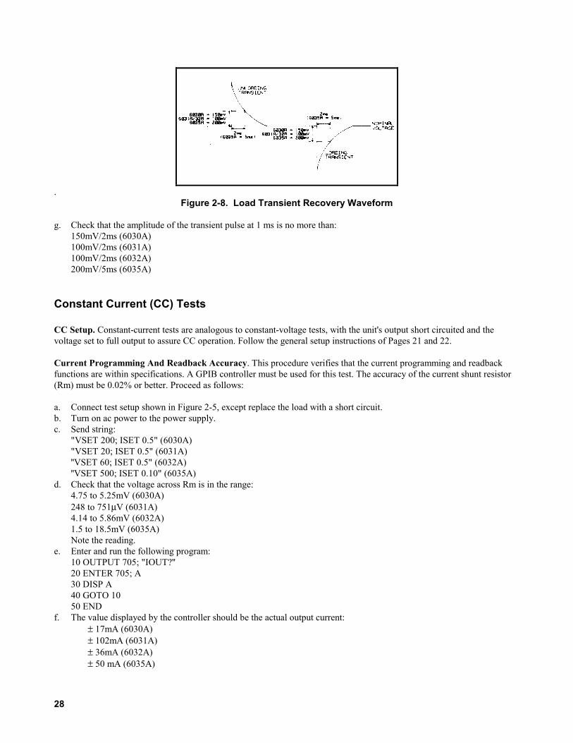
28
.
Figure 2-8. Load Transient Recovery Waveform g. Check that the amplitude of the transient pulse at 1 ms is no more than:
150mV/2ms (6030A)100mV/2ms (6031A)100mV/2ms (6032A)200mV/5ms (6035A)
Constant Current (CC) Tests
CC Setup. Constant-current tests are analogous to constant-voltage tests, with the unit's output short circuited and thevoltage set to full output to assure CC operation. Follow the general setup instructions of Pages 21 and 22.
Current Programming And Readback Accuracy. This procedure verifies that the current programming and readbackfunctions are within specifications. A GPIB controller must be used for this test. The accuracy of the current shunt resistor(Rm) must be 0.02% or better. Proceed as follows:
a. Connect test setup shown in Figure 2-5, except replace the load with a short circuit.b. Turn on ac power to the power supply.c. Send string: "VSET 200; ISET 0.5" (6030A) "VSET 20; ISET 0.5" (6031A) ''VSET 60; ISET 0.5" (6032A) ''VSET 500; ISET 0.10" (6035A)d. Check that the voltage across Rm is in the range: 4.75 to 5.25mV (6030A) 248 to 751µV (6031A) 4.14 to 5.86mV (6032A) 1.5 to 18.5mV (6035A) Note the reading.e. Enter and run the following program: 10 OUTPUT 705; "IOUT?'' 20 ENTER 705; A 30 DISP A 40 GOTO 10 50 ENDf. The value displayed by the controller should be the actual output current:
± 17mA (6030A)± 102mA (6031A)± 36mA (6032A)± 50 mA (6035A)
29
g. Send string: "VSET 200; ISET 17" (6030A) ''VSET 20; ISET 120" (6031A) ''VSET 60; ISET 50" (6032A) ''VSET 500; ISET 5" (6035A)h. Check that the voltage across Rm is in the range: 169.72 to 170.28mV (6030A) 119.4 to 120.55mV (6031A) 498.1 to 501.8 mV (6032A) 490 to 510 mV (6035A) Note the reading.i. Run the program listed in step e.j. The value displayed by the controller should be the actual output current:
± 76mA (6030A)± 580mA (6031A)± 215mA (6032A)± 75mA (6035A)
Load Effect (Load Regulation). Constant current load effect is the change in dc output current (Io) resulting from aload-resistance change from short-circuit to full-load, or full-load to short-circuit. Full-load is the resistance which developsthe maximum rated output voltage at current Io. Proceed as follows:a. Connect the test equipment as shown in Figure 2-5. Operate the load in constant resistance mode (Amps/Volt) and set
resistance to minimum.b. Turn the unit's power on, and, using DISPLAY SETTINGS pushbutton switch, turn up voltage setting to full output.c. Turn up output current to: 5.0Adc (6030A) 50Adc (6031A) 16.5Adc (6032A) 2.0Adc (6035A)d. Increase the load resistance until the output voltage at +S and -S decreases to: 200Vdc (6030A). 20Vdc (6031A). 60Vdc (6032A) 500Vdc (6035A) Check that the CC LED is lighted and AMPS display still reads ≈ current setting.e. Short-circuit the load and allow the voltage across Rm to stabilize.f. Record voltage across Rm.g. Disconnect short across load.h. When the reading settles (≈ 10s), record the voltage across Rm again. Check that the two recorded readings differ no
more than:± 10mA (6030A)± 20mA (6031A)± 11mA (6032A)± 34mA (6035A)
Source Effect (Line Regulation). Constant current source effect is the change in dc output current resulting from a changein ac input voltage from the minimum to the maximum values listed in the Specifications Table in the Operating Manual.Proceed as follows:a. Connect the test equipment as shown in Figure 2-5. Operate the load in constant resistance mode (Amps/Volt) and set
resistance to minimum.b. Connect the unit to the ac power line through a variable autotransformer set for nominal line voltage.c. Switch the unit's power on and turn up output voltage setting to full output.

30
d. Turn up output current to: 17.0Adc (6030A) 120Adc (6031A) 50Adc (6032A) 5.0 Adc (6035A)e. Increase the load resistance until the output voltage between + S and - S decreases to: 60Vdc (6030A) 7.0Vdc (6031A) 20.0Vdc (6032A) 200 Vdc (6035A) Check that the CC LED is still on.f. Adjust autotransformer to the minimum for your line voltage.g. Record the voltage across Rm.h. Adjust autotransformer to the maximum for your line voltage.i. When the reading settles record the voltage across Rm again. Check that the two recorded readings differ no more than:
6mA (6030A)37mA (6031A)15mA (6032A)18 mA (6035A)
PARD Ripple And Noise. Periodic and random deviations (PARD) in the unit's output (ripple and noise) combine toproduce a residual ac current as well as an ac voltage super-imposed on the dc output. The ac voltage is measured asconstant-voltage PARD, Page 23. Constant-current PARD is specified as the root-mean-square (rms) output current in afrequency range 20Hz to 20MHz with the unit in CC operation. To avoid incorrect measurements, with the unit in CCoperation, caused by the impedance of the electronic load at noise frequencies, use a:
3.5Ω (6030A)0.069Ω (6031A)0.4Ω (6032A)40Ω (6035A)
load resistor that is capable of safely dissipating 1000 watts. Proceed as follows:a. Connect the test equipment as shown in Figure 2-9. Note: For Agilent 6031A units, use a 30Adc power supply in the test setup to subtract from the 120Adc of the Agilent 603lA unit under test. This will prevent the current probe specified in Table 2-1 from saturating. Make sure the rms noise of the 30Adc supply is less than 10mA rms. b. Switch the unit's power on and turn the output voltage all the way up.c. Turn up output current to: 17.0Adc (6030A) 120Adc (6031A) 50 Adc (6032A) 5.0 Adc (6035A) Check that the unit's CC LED remains lighted.d. Check that the rms noise current measured by the current probe and rms voltmeter is no more than:
15mA rms (6030A).120mA rms (6031A)25mA rms (6032A)50 mA rms (6035A)
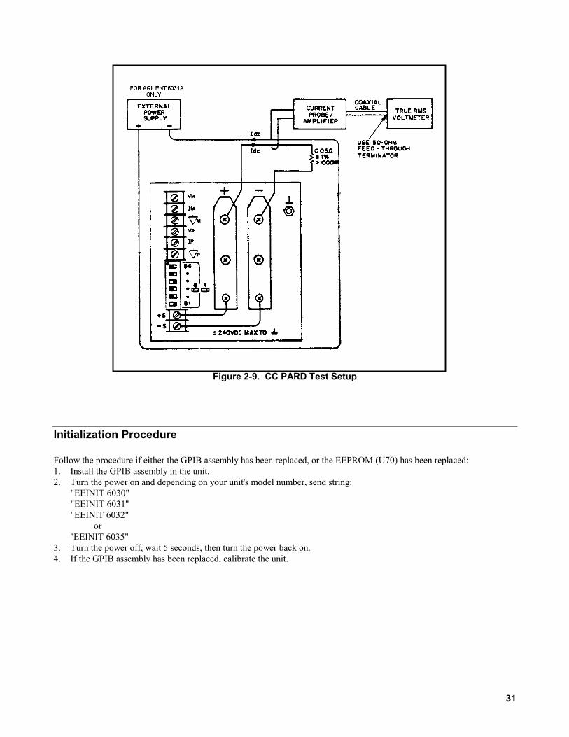
31
Figure 2-9. CC PARD Test Setup
Initialization Procedure
Follow the procedure if either the GPIB assembly has been replaced, or the EEPROM (U70) has been replaced:1. Install the GPIB assembly in the unit.2. Turn the power on and depending on your unit's model number, send string: "EEINIT 6030" "EEINIT 6031'' "EEINlT 6032" or ''EEINIT 6035"3. Turn the power off, wait 5 seconds, then turn the power back on.4. If the GPIB assembly has been replaced, calibrate the unit.

33
3Troubleshooting
Maintenance described herein is performed with power supplied to the instrument, and protective coversremoved. Such maintenance should be performed only by service-trained personnel who are aware of the
hazards involved (for example, fire and electrical shock). Where maintenance can be performed without power applied, the power should be removed.
Introduction
Before attempting to troubleshoot this instrument, ensure that the fault is with the instrument itself and not with anassociated circuit. The performance test enables this to be determined without having to remove the covers from the supply.
The most important aspect of troubleshooting is the formulation of a logical approach to locating the source of trouble. Agood understanding of the principles of operation is particularly helpful, and it is recommended that Chapter 4 of thismanual be reviewed before attempting to troubleshoot the unit. Often the user will then be able to isolate a problem simplyby using the operating controls and indicators. Once the principles of operation are understood, refer to the followingparagraphs.
Table 2-1 lists the test equipment for troubleshooting. Chapter 6 contains schematic diagrams and information concerningthe voltage levels and waveforms at many of the important test points. Most of the test points used for troubleshooting thesupply are located on the control board test "fingers", which are accessible close to the top of the board. See Table 3-9.
If a component is found to be defective, replace it and re-conduct the performance test. When a component is replaced, referto Calibration Procedure (Chapter 2). It may be necessary to perform one or more of the adjustment procedures after acomponent is replaced.
Initial Troubleshooting Procedures
If a problem occurs, follow the steps below in sequence:
a. Check that input power is available, and check the power cord and rear-panel circuit breaker.b. Check that the settings of mode switch A2S1 are correct for the desired mode of operation. (See Operating Manual).c. Check that all connections to the power supply are secure and that circuits between the supply and external devices are
not interrupted.d. Check that the rear-panel GPIB address switch A8S1 is properly set. (See Operating Manual).e. If the power supply fails turn-on self-test or gives any other indication of malfunction, remove the unit from the
operating system before proceeding with further testing.
Some circuits on the power mesh are connected directly to the ac power line. Exercise extreme cautionwhen working on energized circuits. Energize the supply through an isolation transformer to avoid
shorting ac energized circuits through the test instrument's input leads. The isolation transformer must have a power rating of at least 4KVA. During work on energized circuits, the safest practice is to disconnect power, make or change the test connections, and then re-apply power.
Make certain that the supply's ground terminal () is securely connected to an earth ground before applying power. Failure to do so will cause a potential shock hazard that could result in personal injury.
34
Electrostatic Protection
The following caution outlines important precautions which should be observed when working with static sensitivecomponents in the power supply.
This instrument uses components which can be damaged by static charge. Most semiconductors cansuffer serious performance degradation as a result of static charges, even though complete failure may
not occur. The following precautions should be observed when handling static-sensitive devices.
a. Always turn power off before removing or installing printed-circuit boards.b. Always stored or transport static-sensitive devices (all semiconductors and thin-film devices) in conductive material.
Attach warning labels to the container or bag enclosing the device.c. Handle static-sensitive devices only at static-free work stations. These work stations should include special conductive
work surfaces (such as Agilent Part No. 9300-0797) grounded through a one-megohm resistor. Note that metal tabletops and highly conductive carbon-impregnated plastic surfaces are too conductive; they can act as large capacitors andshunt charges too quickly. The work surfaces should have distributed resistance of between 106and 10l2 Ω per square.
d. Ground all conductive equipment or devices that may come in contact with static-sensitive devices or subassembliescontaining same.
e. Where direct grounding of objects in the work area is impractical, a static neutralizer should be used (ionized air blowerdirected at work). Note that this method is considerably less effective than direct grounding and provides less protectionfor static-sensitive devices.
f. While working with equipment on which no point exceeds 500 volts, use a conductive wrist strap in contact with skin.The wrist strap should be connected to ground through a one-megohm resistor. A wrist strap with insulated cord andbuilt-in resistor is recommended, such as 3M Co. No. 1066 (Agilent Part No. 9300-0969 (small) and 9300-0970[large]).
Do not wear a conductive wrist strap when working with potentials in excess of 500 volts; the one-megohmresistor will provide insufficient current limiting for personal safety.
g. All grounding (device being repaired, test equipment, soldering iron, work surface, wrist strap, etc.) should be done tothe same point.
h. Do not wear nylon clothing. Keep clothing of any kind from coming within 12 inches of static-sensitive devices.i. Low-impedance test equipment (signal generators, logic pulsers, etc.) should be connected to static-sensitive inputs
only while the components are powered.j. Use a mildly activated rosin core solder (such as Alpha Metal Reliacor No. 1, Agilent Part No. 8090-0098) for repair.
The flux residue of this type of solder can be left on the printed circuit board. Generally, it is safer not to clean theprinted-circuit board after repair. Do not use Freon or other types of spray cleaners. If necessary, the printed-circuitboard can be brushed using a natural-bristle brush only. Do not use nylon-bristle or other synthetic-bristle brushes. Donot use high-velocity air blowers (unless ionized).
k. Keep the work area free of non-conductive objects such as Styrofoam-type cups, polystyrene foam, polyethylene bags,and plastic wrappers. Non-conductive devices that are necessary in the area can be kept from building up a static chargeby spraying them with an anti-static chemical (Agilent Part No. 8500-3397).
l. Do not allow long hair to come in contact with static-sensitive assemblies.m. Do not exceed the maximum rated voltages specified for the device.
Repair and Replacement
Repair and replacement of most components in the power supply require only standard techniques that should be apparent tothe technician. The following paragraphs provide instructions for removing certain assemblies and components for whichthe procedure may not be obvious upon inspection.
To avoid the possibility of personal injury, remove the power supply from operation before opening thecabinet. Turn off ac power and disconnect the line cord, GPIB plug, load, and remote sense leads before
attempting any repair or replacement.

35
When replacing any heatsink-mounted components except thermostat, smear a thin coating of heatsinkcompound between the component and heatsink. If a mica insulator is used, smear a thin coating of
heatsink compound on both sides of the mica insulator.
Do not use any heatsink compound containing silicone, which can migrate and foul electrical contacts elsewhere in the system. An organic zinc oxide cream, such as American Oil and Supply Company Heatsink Compound #100, is recommended.
Most of the attaching hardware in this unit is metric. The only non-metric (sometimes called English orinch) fittings are listed below. Be careful when both types of screws are removed not to get them mixed
up.
a. Screws that secure the input and output capacitors to A1 main board and output bus bars.b. Rear-panel circuit breaker.c. Rear-panel ground binding post.d. Strap-handle screws (2).e. Screws that secure side chassis to front-frame casting (4, 2 on top and 2 on bottom).
Top Outside Cover Removal. Remove the two top rear screws using a Size 2, Pozidriv screwdriver. A Phillips headscrewdriver does not fully seat into Pozidriv screws and risks stripping the heads. Remove the top cover by sliding it to therear and lifting at the front.
Bottom Cover Removal. Remove the handles from both sides of the unit and remove the bottom cover by sliding it to therear. Use a Phillips head #2 screwdriver to remove the handle screws. You do not need to remove the unit's feet.
Inside Top Cover Removal. The unit includes an inside cover which secures the vertical board assemblies. Remove theinside cover for repair but not for calibration.
Remove the nine mounting screws (Pozidriv, M4x.7) -two on the left side, three on the right side, four on top. Remove theinside cover by lifting at the front edge.
When installing the inside cover, insert it first at the right side. While holding it tilted up at the left, reach through thecutouts in the cover and fit the top tabs of the A8 GPIB board into the mating slots in the cover. Then repeat the process forthe A2 control board, the A4 FET board, and the A5 Diode board. Press the inside cover down firmly while tighteningscrews that secure cover to chassis. Be careful not to bend any boards or components.
A2 Control Board Removal
After removing the inside cover, unplug the W5 and W6 ribbon cables at the top edge of the A2 control board. Then unplugthe W7 and W8 ribbon cables from the lower center of the board. Remove the A2 board by lifting first at the front edge andthan pulling it up and out of the unit.
When installing the A2 board, insert it first at the rear of the unit. While holding it tilted up at the front, fit the A2TB1terminal strip into the mating cutout in the rear panel. Then lower the A2 board's bottom connectors into the matingconnectors on the main board. Press the A2 board into the connectors, and reinstall the W5, W6, W7, and W8 ribboncables.
A4 FET Board Removal
After removing the inside cover, remove the A4 mesh board by lifting, using the large aluminum heatsink as a handle. Oneconnector and one tab holds the A4 board at its bottom edge.

36
When installing the A4 power mesh board, lower it vertically, placing its tab into the A1 board slot, align the connector andpress in place.
A5 Diode Board Removal
After removing the cover, remove the A5 Diode board by first removing the two screws (Pozidriv) that hold heatsinks to theA1 board, then lift vertically to remove the A5 board from the connector.
When installing the A5 Diode board, lower it vertically into the mating connector on the A1 board, then install a screwbetween each heatsink and Al board.
A8 GPIB Board Removal
Remove the A8 board as follows:a. Remove the two screws (Pozidriv, M3x.5) which attach the A8 GPIB board to the rear panel. Remove the single screw
(Pozidriv, M4x.7) that secures the GPIB board to the side frame near the front corner.b. After removing the inside cover, unplug the W5 and W6 ribbon cables at the top edge of the A8 board, the W2 3-wire
cable from connector A8J10 and the W1 ribbon cable from connector A8J9.c. Remove the A8 board lifting it straight up.
Install the A8 board by reversing the above steps. Lower the rear side of the board into the unit first and fit the bottom tabsinto their mating slots.
A3 Front-Panel Board Removal
Remove the A3 front-panel board by first removing the entire front panel assembly. You do not need to remove the topcover. Follow this procedure:a. Remove the top plastic insert by prying up with a flat-blade screwdriver.b. Remove the four front-panel assembly mounting screws (Pozidriv M4) on the top and bottom at the comers.c. Gently pull the front-panel assembly away from the unit as far as permitted by the connecting cables.d. Note the locations of the four power-wire connections to the power switch and then unplug the quick-connect plugs.e. Unplug the W3 3-wire cable from connector A1J4 on the A2 control board, and unplug the W1 ribbon cable from
connector A8J9 on the A8 GPIB board.f. Remove the A3 board from the front-panel assembly by removing the six mounting screws (Pozidriv, M4x.7)
Install the A3 Board by reversing the steps above.
A1 Main Board Removal
Removing the A1 main board requires removing the rear-panel, all boards except the A3 front-panel board, and 17 A1board mounting screws, four standoffs, and two bus bar mounting screws. Component-access cutouts in the bottom insidecover allow unsoldering most A1-board components for repair without removing the A1 board.Proceed as follows
a. Remove the A2, A4, A5, and A8 boards according to the above instructions.b. Remove the AC power cord from the cooling fan and the four AC Input Power wires.

37
AC Input Wire Terminal Destinationfrom color designator location
L6 (chassis) white P left rearRFI filter white/gray N behind A1K1Circuit breaker white/brown/gray L behind A1K1L6 (chassis) white A1K1 front armature
c. Remove the following mounting screws, all Pozidriv: 2 (1 each) from the output bus bars 7 from the A1 board 4 from transformer AlT2 4 from transformer AlT3 2 from relay AlK1 4 inside-cover mounting posts 5/16 hex
d. Lift the A1 board up and toward the rear, then remove the wires from the front panel switch A3S1.
A1 Designator Wire color A3S1 Position (Rear View)A white/grayB gray S1C white/brown/gray B - | - AD white/red/gray C - | - D
Install the A1 board by reversing the above steps. Be careful to follow the wire color code.
Overall Troubleshooting Procedure
The overall troubleshooting procedure for the unit involves isolating the problem to one of several circuit blocks andtroubleshooting the block individually. The GPIB/microprocessor related circuit blocks are located on the A3 (front panel)and the A8 (GPIB) boards. They are referred to collectively as the GPIB section. The power supply circuit blocks are on theA1 (main), the A2 (control), the A4 (FET), and the A5 (diode) boards. They are referred to collectively as the powersection.
The flowchart of Figure 3-1 provides troubleshooting isolation procedures to guide you either to the appropriate circuit or toone of the detailed troubleshooting procedures in this section. The purpose of the flowchart is only to isolate the problem toa specific area of the power supply. If you have already isolated the problem, proceed directly to the applicabletroubleshooting section.
Table 3-1 lists the error codes that may appear on the front panel when the unit performs its internal selftest. Along with theerror codes, the table also identifies various circuits or components that may have caused that error code to appear.
In the Power Section Troubleshooting, Tables 3-10 and 3-11 give various power supply symptoms that identify thecorresponding board, circuit or components that may have caused that symptom. The symptoms in Table 3-10 may becomeapparent when running the Performance Tests in Section 2.
GPIB Section Troubleshooting
The GPIB section troubleshooting consists of primary and secondary interface troubleshooting. Signature analysis isrequired to troubleshoot the primary and secondary processor as well as the front panel board. Other circuits on the GPIBboard, such as the voltage and current DACs, can be checked using either signature analysis or the front panel controls. Thereadback circuits cannot be checked using signature analysis. Figure 3-2 illustrates the test setup that allows access to theGPIB board components for troubleshooting.
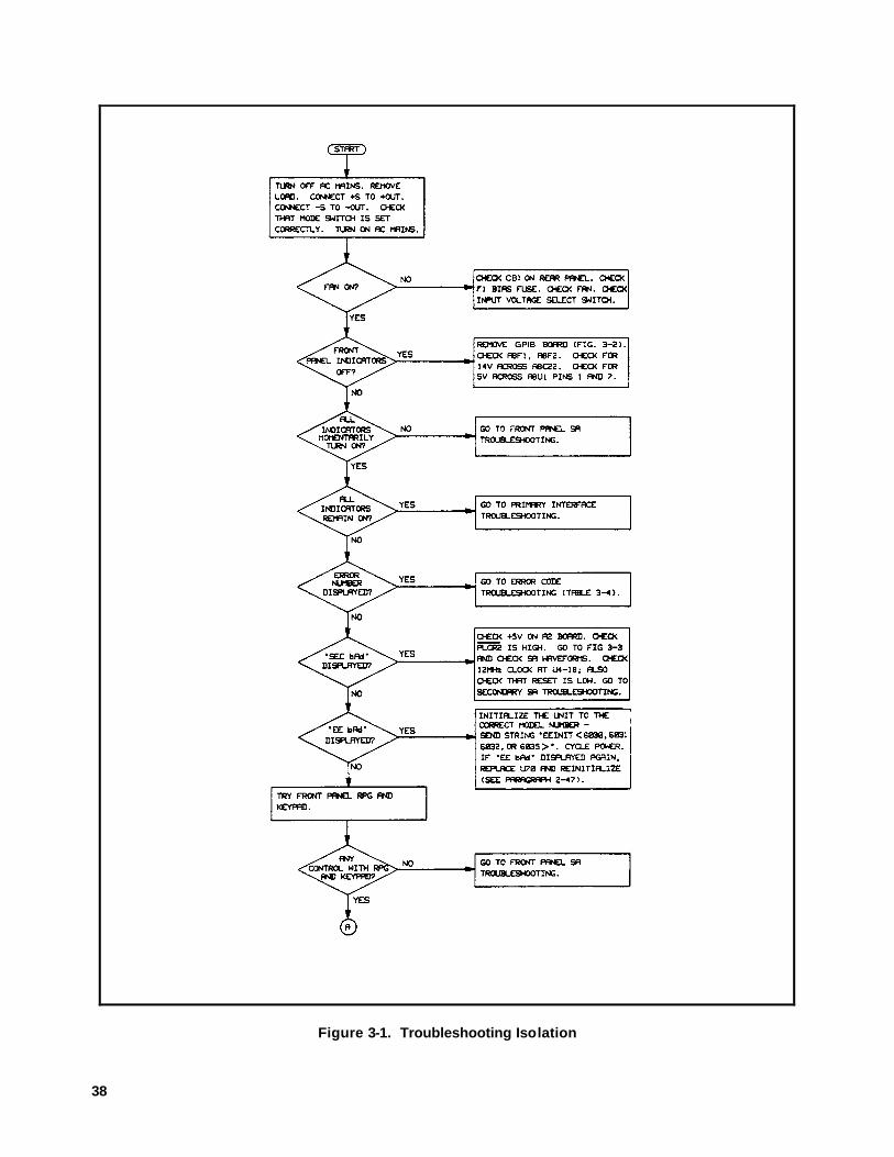
38
Figure 3-1. Troubleshooting Isolation
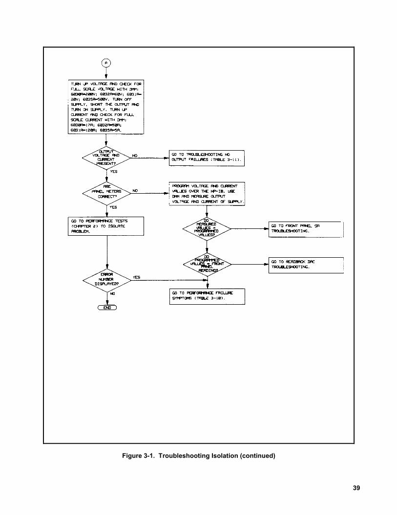
39
Figure 3-1. Troubleshooting Isolation (continued)
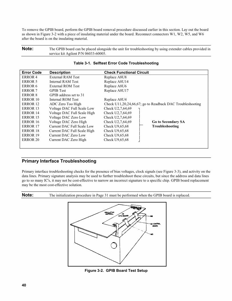
40
To remove the GPIB board, perform the GPIB board removal procedure discussed earlier in this section. Lay out the boardas shown in Figure 3-2 with a piece of insulating material under the board. Reconnect connectors W1, W2, W5, and W6after the board is on the insulating material.
Note: The GPIB board can be placed alongside the unit for troubleshooting by using extender cables provided inservice kit Agilent P/N 06033-60005.
Table 3-1. Selftest Error Code Troubleshooting
Error Code Description Check Functional CircuitERROR 4 External RAM Test Replace A8U8ERROR 5 Internal RAM Test Replace A8U14ERROR 6 External ROM Test Replace A8U6ERROR 7 GPIB Test Replace A8U17ERROR 8 GPIB address set to 31ERROR 10 Internal ROM Test Replace A8U4ERROR 12 ADC Zero Too High Check U11,20,24,66,67; go to Readback DAC TroubleshootingERROR 13 Voltage DAC Full Scale Low Check U2,7,64,69ERROR 14 Voltage DAC Full Scale High Check U2,7,64,69ERROR 15 Voltage DAC Zero Low Check U2,7,64,69ERROR 16 Voltage DAC Zero High Check U2,7,64,69ERROR 17 Current DAC Full Scale Low Check U9,65,68ERROR 18 Current DAC Full Scale High Check U9,65,68ERROR 19 Current DAC Zero Low Check U9,65,68ERROR 20 Current DAC Zero High Check U9,65,68
Go to Secondary SATroubleshooting
Primary Interface Troubleshooting
Primary interface troubleshooting checks for the presence of bias voltages, clock signals (see Figure 3-3), and activity on thedata lines. Primary signature analysis may be used to further troubleshoot these circuits, but since the address and data linesgo to so many IC's, it may not be cost-effective to narrow an incorrect signature to a specific chip. GPIB board replacementmay be the most cost-effective solution.
Note: The initialization procedure in Page 31 must be performed when the GPIB board is replaced.
Figure 3-2. GPIB Board Test Setup

41
+5V and PCLR Circuits:
Node MeasurementU1-8 ≈ 3.5VdcU1-2 = 4 VdcU1-3 = 4.2VdcU1-4 = 4.2VdcU1-6 ≈50mVdc
Clock Signals (see clock waveforms in Figure 3-3)
Node Measurement SourceC7+,C8+ = 12MHz (see waveform) Y2J5-8 = 6MHz (see waveform) U14U35-12 ≈ 50mVdc (see waveform) U35
Data Lines Check that all data and address lines are toggling. Address and data lines go to the following IC's:
Address Lines Data LinesU6: A0 to A15 U6: D0 to D7U8: A0 to A15 U8: D0 to D7U12: A0 to A4 U12: D0 to D7U14: A8 to A15 U14: D0 to D7U16: A0 to A7 U16: D0 to D7U17: A0 to A2 U17: D0 to D7U36: A7 to A15
Note: Data and address lines may not toggle if one line is shorted either high or low. If no short is found, replaceall socketed IC's. If the data lines still do not toggle, replace the GPIB (A8) assembly.
Node MeasurementA0 to A15 TogglingD0 to D7 Toggling
Secondary Interface Troubleshooting
Secondary interface troubleshooting checks the operation of the voltage, current, and readback DACs as well as analogmultiplexer and secondary microprocessor. The analog multiplexer is checked in the Readback DAC troubleshootingprocedure. The secondary microprocessor can only be checked using secondary SA (refer to Signature Analysis).
Voltage and Current DAC
The voltage and current DACs can be checked either from the front panel or by secondary SA. Refer to Signature Analysisto troubleshoot the voltage and current DACs in this manner.
Note: To troubleshoot the voltage and current DACs from the front panel if the unit has failed selftest, placejumper A8J5 in the skip selftest position (see Table 3-2). This lets you operate the unit even though it failsthe internal selftest.

42
Figure 3-3. Clock and Primary SA Waveforms
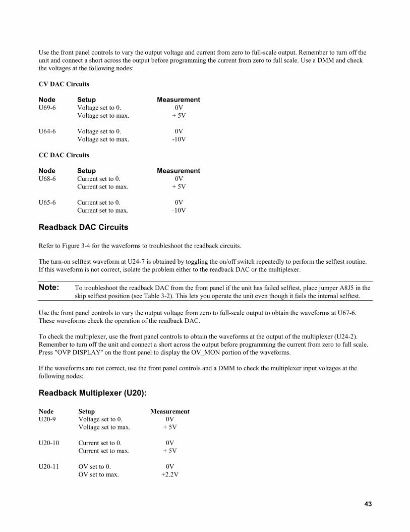
43
Use the front panel controls to vary the output voltage and current from zero to full-scale output. Remember to turn off theunit and connect a short across the output before programming the current from zero to full scale. Use a DMM and checkthe voltages at the following nodes:
CV DAC Circuits
Node Setup MeasurementU69-6 Voltage set to 0. 0V
Voltage set to max. + 5V
U64-6 Voltage set to 0. 0VVoltage set to max. -10V
CC DAC Circuits
Node Setup MeasurementU68-6 Current set to 0. 0V
Current set to max. + 5V
U65-6 Current set to 0. 0VCurrent set to max. -10V
Readback DAC Circuits
Refer to Figure 3-4 for the waveforms to troubleshoot the readback circuits.
The turn-on selftest waveform at U24-7 is obtained by toggling the on/off switch repeatedly to perform the selftest routine.If this waveform is not correct, isolate the problem either to the readback DAC or the multiplexer.
Note: To troubleshoot the readback DAC from the front panel if the unit has failed selftest, place jumper A8J5 in theskip selftest position (see Table 3-2). This lets you operate the unit even though it fails the internal selftest.
Use the front panel controls to vary the output voltage from zero to full-scale output to obtain the waveforms at U67-6.These waveforms check the operation of the readback DAC.
To check the multiplexer, use the front panel controls to obtain the waveforms at the output of the multiplexer (U24-2).Remember to turn off the unit and connect a short across the output before programming the current from zero to full scale.Press "OVP DISPLAY'' on the front panel to display the OV_MON portion of the waveforms.
If the waveforms are not correct, use the front panel controls and a DMM to check the multiplexer input voltages at thefollowing nodes:
Readback Multiplexer (U20):
Node Setup MeasurementU20-9 Voltage set to 0. 0V
Voltage set to max. + 5V
U20-10 Current set to 0. 0VCurrent set to max. + 5V
U20-11 OV set to 0. 0VOV set to max. +2.2V
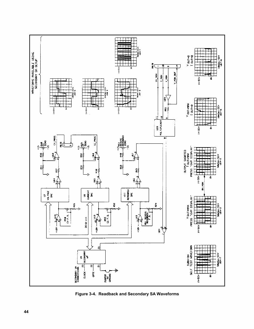
44
Figure 3-4. Readback and Secondary SA Waveforms
45
Signature Analysis
Perform the signature analysis only after you have completed the Primary Processor Troubleshooting.
The easiest and most efficient method of troubleshooting microprocessor-based instruments is signature analysis. Signatureanalysis is similar to signal tracing with an oscilloscope in linear circuits. Part of the microcomputer memory is dedicated tosignature analysis and a known bit stream is generated to stimulate as many nodes as possible within the circuit. However,because it is virtually impossible to analyze a bit stream with an oscilloscope, a signature analyzer is used to compress thebit stream into a four-character signature that is unique for each node. By comparing signatures of the unit under test to thecorrect signatures for each node, faults can usually be isolated to one or two components. Note that signature analysisprovides only go/no-go information; the signature provides absolutely no diagnostic information.
The following general notes apply to signature analysis of the power supply.
1. Be certain to use the correct setup for the signature being examined.2. Most signatures are taken on the GPIB, and front panel assemblies.3. Note the signatures for Vcc and ground on the I.C. being examined. If an incorrect signature is the same as that of Vcc
or ground, that point is probably shorted to Vcc or ground.4. If two pins have identical signatures, they are probably shorted together. If two signatures are similar, it is only
coincidence. For example, if the signature at a certain point should be 65C4, a signature of 65C3 is not "almost right".No diagnostic information can be inferred from an incorrect signature.
5. If a signature is incorrect at an input pin, but is correct at its source (output of previous I.C.), check for printed circuitand soldering discontinuity.
6. An incorrect signature at an output could be caused by a faulty component producing that output; or, a short circuit inanother component or on the board could be loading down that node.
Tables 3-2 and 3-3 show the primary, front panel, and secondary signature analyzer connections that are required to performthe SA tests in Tables 3-4 through 3-8. Remember that the primary and secondary circuits each reference a different circuitcommon.
Primary SA
Place the unit in primary SA mode by moving the J5 jumper as shown in Table 3-2. Connect the signature analyzer asshown in the table. The front panel display should indicate: ''SA SA", and all LED's will be on. If the display is different,replace U14.
Note: The power supply will not go into SA mode if one of the data and address lines is shorted either high orlow. Refer to Data Lines troubleshooting.
When the unit is in SA mode, check for the waveforms shown in Figure 3-3. Refer to Table 3-4 for the primary SAsignatures. Return the J5 jumper to its normal position when the primary signature analysis is complete.
Front Panel SA
To place the unit in SA mode for Front Panel SA troubleshooting, follow the procedure for Primary SA troubleshooting.When the unit is in SA mode, check the signatures in Tables 3-5 through 3-7.
The signatures in Table 3-5 check the registers that drive the 7-segment LED displays. Most problems will involve only onedisplay or LED indicator. Table 3-6 checks the address latches and decoders. Address latch U15 forwards address data tothe address decoders, which enable the shift registers. Table 3-7 checks flip-flop U12, shift register U11, and gate U18. U12decodes the output of the RPG. U11 and U18 are used by the microprocessor to read the status of the RPG and front panelswitches.

46
Return the J5 jumper to its normal position when the front panel signature analysis is complete.
Secondary SA
For secondary SA troubleshooting, connect the signature analyzer as shown in Table 3-3. Use a jumper wire and short U4pin 21 to common (U4 pin 20). Check for the waveforms in Figure 3-4 and the signatures in Table 3-8 for the secondarySA. When the secondary signature analysis is complete, disconnect the jumper on U4 pin 21.
Table 3-2. Primary and Front Panel Signature Analyzer Test Setups
SIGNATUREANALYZER INPUT
EDGESETTING
PRIMARY SACONNECTIONS
CLOCKSTARTSTOP
GROUND
A8J5 pin 8A8U37 pin 16A8U37 pin 16
A8J5 pin 5A8J5 (in SA mode)
A8J5 JUMPER POSITIONSJumpering pins 1 and 2 skips the internalselftest when the unit is turned on.Jumpering pins 3 and 4 places U37 in SA mode.Jumpering pins 5 and 6 is the normal/operatingposition of the jumper.
Table 3-3. Secondary Signature Analyzer Test Setups
SIGNATUREANALYZER INPUT
EDGESETTING
SECONDARY SACONNECTIONS
CLOCKSTARTSTOP
GROUND
A8U4 pin 23A8U4 pin 22A8U4 pin 22A8U4 pin 20
A8U4 JUMPER POSITIONSUse a jumper wire and connect A8U4 pin 21 to pin 20 (ground).
Use a 40-pin test clip (Pomona Model 5240 or eq.) to facilitate testconnections to A8U4.

47
Table 3-4. Primary Processor Signature Table(A8U6 = P/N 5080-2160 REV A.00.00, A.00.01, A.00.02 and A.00.04)
A.00.04 A.00.02 A.00.01 A.00.00A(0) A46A A46A A46A A46A U16-12 U6-12 U8-12 U12-11 U17-21A(1) 4148 UH8O UH8O UH8O U16-13 U6-11 U8-11 U12-13 U17-22A(2) 72F5 82H5 UO39 4FU1 U16-14 U6-10 U8-10 U12-9 U17-23A(3) PAU8 9899 HOPF 86C2 U16-15 U6-9 U8-9 U12-10A(4) A4A7 3088 O7FA 5A37 U16-16 U6-8 U8-8 U12-8A(5) 45OP 48H5 5823 PHHO U16-17 U6-7 U8-7A(6) C3UU UF3H 2682 3F6U U16-18 U6-6 U8-6 U36-11A(7) HOU4 HOU4 F6OP HFP3 U16-19 U6-5 U8-5 U36-9A(8) 4U39 4U39 17AF 17AF U14-52 U6-27 U8-27 U36-8A(9) 45A8 45A8 62H1 62H1 U14-51 U6-26 U8-26 U36-7A(10) 278A 278A OOU3 OOU3 U14-50 U6-23 U8-23 U36-6A(11) 6OA3 6OA3 6OA3 6OA3 U14-49 U6-25 U8-25 U36-5A(12) 7826 7826 7826 7826 U14-48 U6-4 U8-4 U36-4A(13) 5850 5850 5850 585O U14-47 U6-28 U8-28 U36-3A(14) F93H F93H F93H F93H U14-46 U6-29 U8-3 U36-2A(15) 79UA 79UA 79UA 79UA U14-45 U6-3 U8-31 U36-1
D(0) PH2F 48P2 48P2 48P2 U14-60 U16-9 U6-13 U8-13 U12-22 U17-12D(1) HU9O 6O84 6O84 6O84 U14-59 U16-8 U6-14 U8-14 U12-21 U17-13D(2) U665 74UH 96C5 HA6P U14-58 U16-7 U6-15 U8-15 U12-20 U17-14D(3) 53PP 16A9 UH79 8OC2 U14-57 U16-6 U6-17 U8-17 U12-19 U17-15D(4) C9C2 196F AA13 U64C U14-56 U16-5 U6-18 U8-18 U12-18 U17-16D(5) C27C 132C 8A9F 89AP U14-55 U16-4 U6-19 U8-19 U12-17 U17-17D(6) HO18 4387 497F 2C5F U14-54 U16-3 U6-20 U8-20 U12-16 U17-18D(7) P97H 4FC3 33AO U44P U14-53 U16-2 U6-21 U8-21 U12-15 U17-19
WR* FP65 FP65 FP65 FP65 U14-40 U8-29 U36-12RD* unstable 3PPH 3PPH 3PPH U14-61 U6-24 U8-24 U36-13ALE U665 4OAP 4OAP 4OAP U14-62 U16-11READY 26C3 26C3 26C3 26C3 U14-43 U36-15
BANK_SEL unstable 5AHH unstable unstable U14-27 U36-14
EE(0) 7CF1 7CF1 7CF1 7CF1 U14-19 U70-1EE(1) AH32 AH32 AH32 AH32 U14-20 U70-2EE(2) HCCH HCCH HCCH HCCH U14-21 U70-3EE(3) 9P5F 9P5F 9P5F 9P5F U14-22 U704
APC 9361 9361 9361 9361 U14-23 U15-22UART CHU5 CHU5 CHU5 CHU5 U12-14 U36-16GPIB 2688 2688 2688 2688 U36-17 U17-8ROM C95F C95F C95F C95F U6-22 U36-19RAM 9UPU 9UPU 9UPU 9UPU U8-22 U36-18
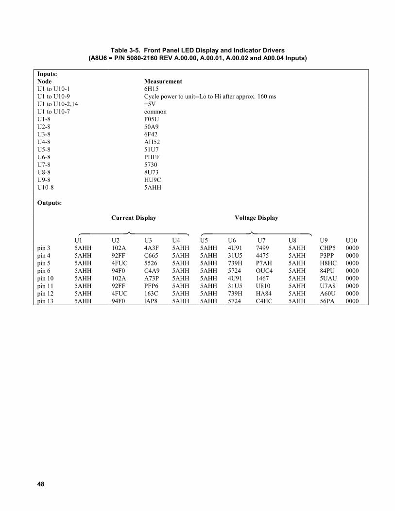
48
Table 3-5. Front Panel LED Display and Indicator Drivers(A8U6 = P/N 5080-2160 REV A.00.00, A.00.01, A.00.02 and A00.04 Inputs)
Inputs:Node MeasurementU1 to U10-1 6H15U1 to U10-9 Cycle power to unit--Lo to Hi after approx. 160 msU1 to U10-2,14 +5VU1 to U10-7 commonU1-8 F05UU2-8 50A9U3-8 6F42U4-8 AH52U5-8 51U7U6-8 PHFFU7-8 5730U8-8 8U73U9-8 HU9CU10-8 5AHH
Outputs:
Current Display Voltage Display
U1 U2 U3 U4 U5 U6 U7 U8 U9 U10pin 3 5AHH 102A 4A3F 5AHH 5AHH 4U91 7499 5AHH CHP5 0000pin 4 5AHH 92FF C665 5AHH 5AHH 31U5 4475 5AHH P3PP 0000pin 5 5AHH 4FUC 5526 5AHH 5AHH 739H P7AH 5AHH H8HC 0000pin 6 5AHH 94F0 C4A9 5AHH 5AHH 5724 OUC4 5AHH 84PU 0000pin 10 5AHH 102A A73P 5AHH 5AHH 4U91 1467 5AHH 5UAU 0000pin 11 5AHH 92FF PFP6 5AHH 5AHH 31U5 U810 5AHH U7A8 0000pin 12 5AHH 4FUC 163C 5AHH 5AHH 739H HA84 5AHH A60U 0000pin 13 5AHH 94F0 lAP8 5AHH 5AHH 5724 C4HC 5AHH 56PA 0000
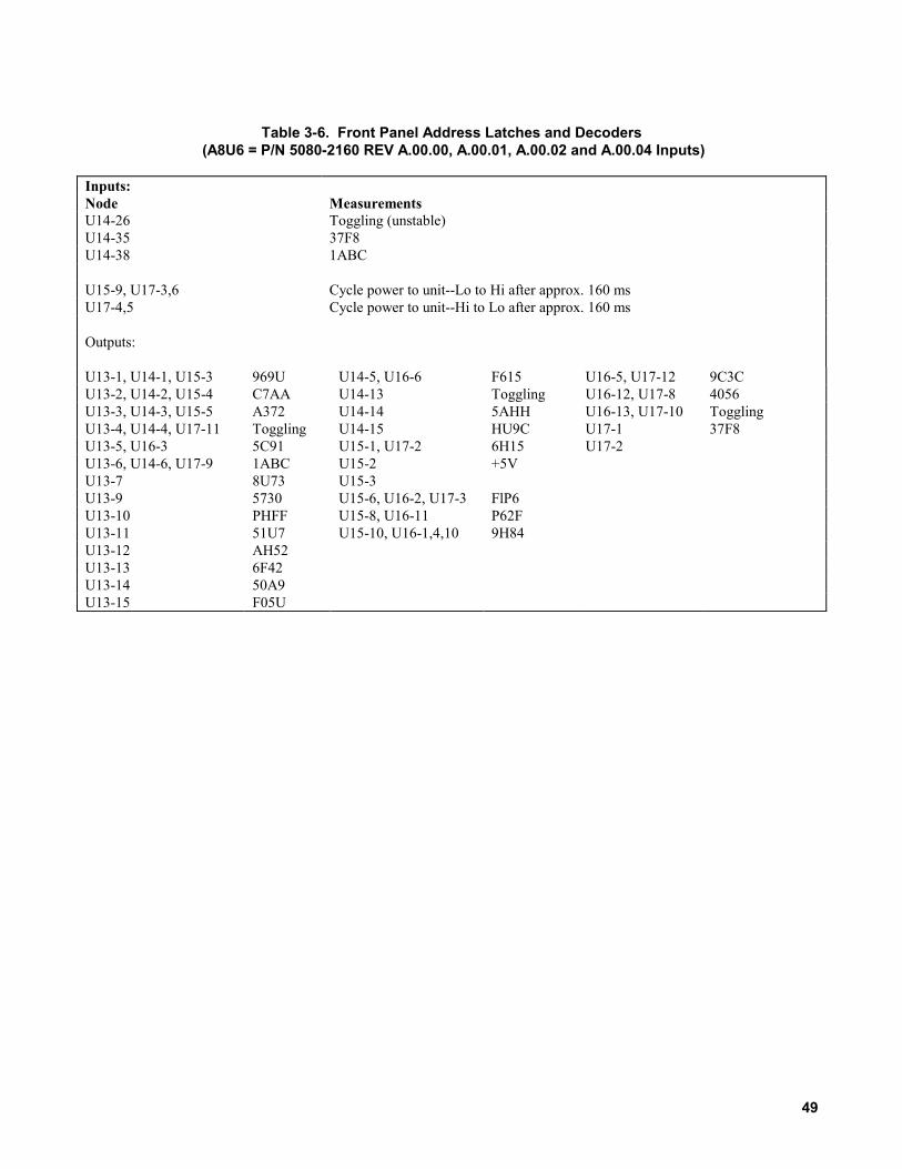
49
Table 3-6. Front Panel Address Latches and Decoders (A8U6 = P/N 5080-2160 REV A.00.00, A.00.01, A.00.02 and A.00.04 Inputs)
Inputs:Node MeasurementsU14-26 Toggling (unstable)U14-35 37F8U14-38 1ABC
U15-9, U17-3,6 Cycle power to unit--Lo to Hi after approx. 160 msU17-4,5 Cycle power to unit--Hi to Lo after approx. 160 ms
Outputs:
U13-1, U14-1, U15-3 969U U14-5, U16-6 F615 U16-5, U17-12 9C3CU13-2, U14-2, U15-4 C7AA U14-13 Toggling U16-12, U17-8 4056U13-3, U14-3, U15-5 A372 U14-14 5AHH U16-13, U17-10 TogglingU13-4, U14-4, U17-11 Toggling U14-15 HU9C U17-1 37F8U13-5, U16-3 5C91 U15-1, U17-2 6H15 U17-2U13-6, U14-6, U17-9 1ABC U15-2 +5VU13-7 8U73 U15-3U13-9 5730 U15-6, U16-2, U17-3 FlP6U13-10 PHFF U15-8, U16-11 P62FU13-11 51U7 U15-10, U16-1,4,10 9H84U13-12 AH52U13-13 6F42U13-14 50A9U13-15 F05U

50
Table 3-7. Front Panel RPG Latches and Input Port(A8U6 = P/N 5080-2160 REV A.00.00, A.00.01 A.00.02, and A.00.04)
Inputs:Node MeasurementU11-1 1ABCU11-2 U12-4,10 Toggling (unstable)U16-10 9H84
Procedure:
NodeS1 LCL released U11-13 Lo U11-7, U16-9 Lo U16-8 HiS1 LCL depressed U11-13 Hi U11-7, U16-8,9 Toggling
S2 OUTPUT ADJUST released U11-14 Lo U11-7, U16-9 Lo U16-8 HiS2 OUTPUT ADJUST depressed U11-14 Hi U11-7, U16-8,9 Toggling
S3 DISPLAY OVP released U11-3 Lo U11-7, U16-9 Lo U16-8 HiS3 DISPLAY OVP depressed U11-3 Hi U11-7, U16-8,9 Toggling
S4 DISPLAY SETTINGS released U11-4 Lo U11-7, U16-9 Lo U16-8 HiS4 DISPLAY SETTINGS depressed U11-4 Hi U11-7, U16-8,9 Toggling
S5 FOLDBACK released U11-5 Lo U11-7, U16-9 Lo U16-8 HiS5 FOLDBACK depressed U11-5 Hi U11-7, U16-8,9 Toggling
U12-5 Node toggles when RPG is rotated clockwiseU12-9 Node toggles when RPG is rotated in either directionSet scope for dual trace operation, 2V/div, 10 ms/div, normal triggering, and positive edge on channel A.Connect channel A to U12-3 and channel B to U12-2.
U12-3 Rotate RPG CW
U12-2 Rotate RPG CW
U12-3 Rotate RPG CCW
U12-2 Rotate RPG CCW

51
Table 3-8. Secondary Processor Signature Table
DS(0) P36U U4-1 U7-15 U9-15 U11-15DS(1) 2280 U4-2 U7-14 U9-14 U11-14DS(2) 4277 U4-3 U7-13 U9-13 U11-13DS(3) 720F U4-4 U7-12 U9-12 U11-12DS(4) 6A31 U4-5 U7-11 U9-11 U11-11DS(5) 662U U4-6 U7-10 U9-10 U11-10DS(6) 6020 U4-7 U7-9 U9-9 U11-9DS(7) 6327 U4-8 U7-8 U9-8 U11-8DS(8) 1377 U4-39 U7-7 U9-7 U11-7 U2-16DS(9) FF99 U4-38 U7-6 U9-6 U11-6 U2-17DS(10) 236P U4-37 U7-5 U9-5 U11-5 U2-18DS(11) H495 U4-36 U7-4 U9-4 U11-4 U2-19
WR* 9FU7 U4-12 U7-17WR* 9FF7 U4-13 U9-17WR* 9FHU U4-14 U11-17
F817 U4-26 U20-136U7 U4-27 U20-160562 U4-28 U20-15
ISTX 9F97 U4-11 U2-4, 149FH6 U4-17 U2-29FH5 U4-16 U2-11
ALE 0000 U4-30 U2-1AU68 U4-35
+ 5V 9FA8 U4-33,34
Power Section Troubleshooting
Table 3-9 describes the signals at each of the control board test points. The test connector provided in service kit P/N5060-2865 allows easy connection to each test point. The measurements given here include bias and reference voltages aswell as power supply status signals. It provides conditions for these measurements and gives the components which are thesources of the signals. Tables 3-10 and 3-11 describe possible symptoms in the power section. Both give lists of circuitblocks or components which can cause the symptoms shown. The appropriate assembly is also given.
If the supply exhibits a symptom given in Table 3-10 or 3-11, go to the block which pertains to that symptom. If the exactsymptom seen is not in the tables, start with the symptom that seems to be closest to the one observed. The blocks are givenin the Power Section Blocks section starting in Paragraph 3-84. Troubleshooting information for each block will include abrief description of the circuit. The columns provided are as follows:
NODE: This column lists the nodes where the measurements should be taken. In some cases this will bestated as NODE( + ) and NODE(-) where the first is the test node and the second is the reference.
SETUP: If a certain setup is required for the measurement, it will be given in this column.
MEASUREMENT: This column indicates what the expected measurement is for the given node.
SOURCE: If applicable, the components which generate the signal will be provided in this column.

52
The A4 FET Board should only be raised on an extender when using the main troubleshooting setup.NEVER use a FET Board extender when the unit is operated with its normal ( ≈ 320Vdc) bus voltage. To
do so is a personal shock hazard and can damage the power supply.
To troubleshoot the power supply the A4 power FET board and A2 control board can be raised out of the unit usingextender boards and cables provided in service kit P/N 5060-2865.
Main Troubleshooting Setup
Figure 3-5 shows the troubleshooting setup for troubleshooting all of the unit except the front panel and initial no-outputfailures (see Paragraph 3-82). The external power supply provides the unit's internal bus voltage. The ac mains connectsdirectly to the unit's A1T3 bias transformer via the isolation transformer, thereby energizing the bias supplies, but it does notconnect to the input rectifier and filter to create the bus voltage. With the external supply the unit operates as a dc-to-dcconverter. The supply biases A4Q1, A4Q2, A4Q3, and A4Q4 PFETs with a low voltage rather than the 320Vdc busvoltage. This protects the PFETs from failure from excess power dissipation if the power-limit comparator or the off-pulsecircuitry are defective. It also reduces the possibility of electrical shock to the troubleshooter.
Figure 3 5. Main Troubleshooting Setup

53
An isolation transformer provides ac voltage that is not referenced to earth ground, thereby reducing thepossibility of accidentally touching two points having high ac potential between them. Failure to use an
isolation transformer as shown in Figure 3-5 will cause the ac mains voltage to be connected directly to many components and circuits within the power supply, including the FET heatsinks, as well as to the terminals of the external dc power supply. Failure to use an isolation transformer is a definite personal- injury hazard.
The troubleshooting setup of Figure 3-5 connects high ac voltage to relay K1, fan B1, fuseholder A1F1, and other components and circuits along the front of the A1 main board.
As a convenience in implementing the troubleshooting setup, modify a spare mains cord set as shown in Figure 3-6. Thisfacilitates connecting the unit's power receptacle to the external supply and connecting the bias transformer to the ac mains.
With the mains cord unplugged proceed as follows:
a. Remove the top cover and the inside cover per Page 35. Remove fuse A1F1.
Failure to remove fuse AlF1 will result in damage to the power supply, damage to the external dc supply,and is an electrical shock hazard to you.
a. Install control board test connector onto the A2J7 card-edge fingers.b. Connect a 50Ω 10-W load resistor to the unit's output terminals.c. The external dc power supply can be connected to the unit in either of two ways (in either case, the front panel LINE
switch should be off):1. Remove white/gray wire from main board terminal marked "N'' (at left side, just behind relay at front left
corner), and remove white/brown, gray wire from terminal "L". Connect external dc power supply to terminals"N" and "L''. Either polarity is correct.
OR2. Ensure that the rear-panel circuit breaker is on. Connect external dc power supply to ac input terminals ''N"
and ''L''. Either polarity is correct.
e. Complete the setup of Figure 3-5 by attaching an ac mains cord to test points J8 (L, black wire) and J7 (N, white wire)and connect the green ground wire to the unit's case ground terminal or a suitably grounded cabinet screw. Connect themains cord to an isolation transformer.
Troubleshooting No-Output Failures
No-output failures often include failure of the A4Q1, A4Q2, A4Q3, and A4Q4 PFETs and their fuses A4F1 and A4F2.When either the off-pulses or the power-limit comparator fails, the PFETs can fail from excessive power dissipation. Thestrategy for localizing no-output failures is to check the voltages and waveforms at the control board test connector topredict if that circuit failure would cause the FETs to fail. This makes it possible to develop your troubleshooting approachwithout an extensive equipment setup. Proceed as follows:
a. With the mains cord disconnected remove the A4 FET board per Page 36. Connect the mains cord and switch onpower.
b. Using Table 3-9 check the bias voltages, the PWM-OFF and PWM-ON Control signals and other signals of interest atthe A2 control board test fingers, A2J7.
c. Check for the presence of program voltages, VP and IP, at the rear panel.d. Check for presence of the 320Vdc rail voltage with + at the rear facing end of AlR3 and - at the rear facing end of
AlR1. If there is no rail voltage, check AlU1.

54
AlR1, AlR3, and AlU1 connect to the ac mains voltage. Use a voltmeter with both input terminals floatingto measure the rail voltage.
a. Select the functional circuit for troubleshooting based on your measurements and Table 3-11, which provides directionbased on the status of the PWM OFF and PWM ON signals.
Figure 3-6. Modified Mains Cord Set For Troubleshooting
Power Section Blocks
This section contains the blocks referenced in Tables 3-10 and 3-11.
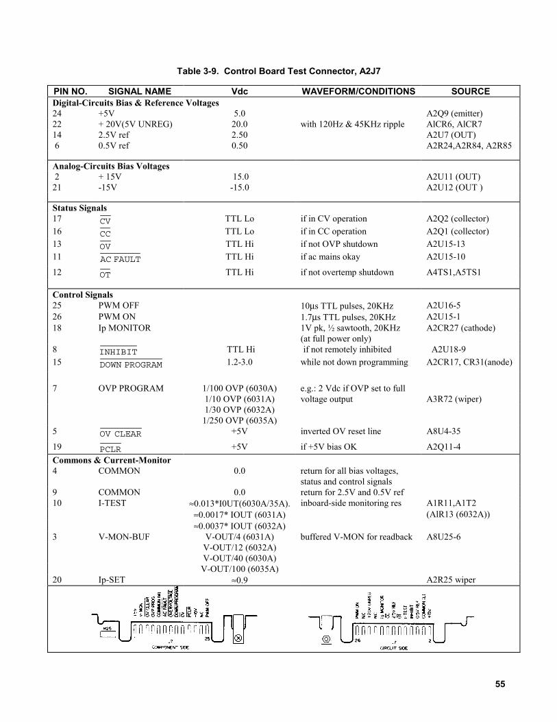
55
Table 3-9. Control Board Test Connector, A2J7
PIN NO. SIGNAL NAME Vdc WAVEFORM/CONDITIONS SOURCEDigital-Circuits Bias & Reference Voltages24 +5V 5.0 A2Q9 (emitter)22 + 20V(5V UNREG) 20.0 with 120Hz & 45KHz ripple AlCR6, AlCR714 2.5V ref 2.50 A2U7 (OUT) 6 0.5V ref 0.50 A2R24,A2R84, A2R85
Analog-Circuits Bias Voltages 2 + 15V 15.0 A2U11 (OUT)21 -15V -15.0 A2U12 (OUT )
Status Signals17 CV TTL Lo if in CV operation A2Q2 (collector)16 CC TTL Lo if in CC operation A2Q1 (collector)13 OV TTL Hi if not OVP shutdown A2U15-1311 AC FAULT TTL Hi if ac mains okay A2U15-10
12 OT TTL Hi if not overtemp shutdown A4TS1,A5TS1
Control Signals25 PWM OFF 10µs TTL pulses, 20KHz A2U16-526 PWM ON 1.7µs TTL pulses, 20KHz A2U15-118 Ip MONITOR 1V pk, ½ sawtooth, 20KHz A2CR27 (cathode)
(at full power only)8 INHIBIT TTL Hi if not remotely inhibited A2U18-915 DOWN PROGRAM 1.2-3.0 while not down programming A2CR17, CR31(anode)
7 OVP PROGRAM 1/100 OVP (6030A) e.g.: 2 Vdc if OVP set to full1/10 OVP (6031A) voltage output A3R72 (wiper)1/30 OVP (6032A)
1/250 OVP (6035A)5 OV CLEAR +5V inverted OV reset line A8U4-35
19 PCLR +5V if +5V bias OK A2Q11-4Commons & Current-Monitor4 COMMON 0.0 return for all bias voltages,
status and control signals9 COMMON 0.0 return for 2.5V and 0.5V ref10 I-TEST ≈0.013*I0UT(6030A/35A). inboard-side monitoring res A1R11,A1T2
≈0.0017* IOUT (6031A) (AlR13 (6032A))≈0.0037* IOUT (6032A)
3 V-MON-BUF V-OUT/4 (6031A) buffered V-MON for readback A8U25-6V-OUT/12 (6032A)V-OUT/40 (6030A)
V-OUT/100 (6035A)20 Ip-SET ≈0.9 A2R25 wiper

56
Table 3-10. Performance Failure Symptoms
DEFECTIVE SYMPTOMS BOARD CHECK FUNCTIONAL CIRCUITS
unexplained OVP shutdowns A2 OVP circuit, CV circuitno current limit A2 CC circuitmax current < specified A2 CC Clamp, CC circuitmax power < specified A2, A1 Power Limit, 20KHz clock, transformer AlT1max voltage < specified A2, A1 CV Circuit, diodes A1CR1-CR4cycles on & off randomly A2, A1 AC-Surge-&-Dropout Detector, Mains Voltage
Select switch A1S2CV overshoots A2 A2U5A, A2CR19, A2R62output noise (<1KHz) A2,A1 CV circuit, input filteroutput noise (>1KHz) A1, A4 transformer AlT2, Output Filter, snubbers A4R1 to
A4R11, A4R13 to A4R19, A4C1 to A4C4, A4CR2,A4CR3, A2R15, A2C2
CV regulation, transient A2, A1 wrong sensingresponse, programming time low ac mains voltage, CV circuitCC regulation A2 low ac mains voltage, CC circuitCV oscillates with capacitive A2 A2R61, A2R60, A2R58, A2R59, A2C33, A2R64,loads A2R68, A2C36, A2C37, A2U5, A2R65CC oscillates with inductive A2 A2R61, A2R60, A2R58, A2R57, A2C33, A2R19loads A2C11, A2R28, A2C12, A2U4, A2R35, A2C20,
A2U4, A2R37, A2C17, A2R29, A2C18, A2R31
Table 3-11. No-Output Failures(Bias supplies and AC turn-on circuit functioning)
Status of FET On/Off-Pulses
PWM-ONA2J7-26
PWM-OFFA2J7-25
DEFECTIVEBOARD
CHECK FUNCTIONAL CIRCUITS
Lo Lo A2 Control ckts: CV & CC thru On- & Off-Pulse Oneshots *Lo Hi A2&A4 PWM and DC-to-DC Converter: A4 PFETS probably failedHi Lo A2&A4 PWM and DC-to-DC Converter: A4 PFETS probably failedHi Hi A2&A4 PWM and DC-to-DC Converter: A4 PFETS probably failedLo N A2 A2U15A, On-Pulse Oneshot and Q11N Lo A2&A4 Off-Pulse Oneshot and DC-to-DC: A4 PFETS probably failedHi N A2&A4 A2U15A, On-Pulse Oneshot & DC-to-DC: A4 PFETS probably failedN Hi A2&A4 Off-Pulse Oneshot and DC-to-DC: A4 PFETS probably failedN N A2&A4 Power-Limit Comparator and DC-to-DC: A4 PFETS probably failed
Lo= TTL low Hi= TTL high N= normal 20KHz pulse train, TTL levels* Decide which to troubleshoot--the CV circuit, the CC circuit, or the PWM and Off-Pulse & On-Pulse Oneshots-- bymeasuring the CV CONTROL (A2CR24, cathode) and the CC CONTROL (A2CR11 cathode) voltages. Troubleshootwhichever is negative, and if neither is negative, troubleshoot the PWM. Make these voltage measurements after youhave implemented the Main Troubleshooting Setup.

57
Troubleshooting AC-Turn-On Circuits
Relay AlK1 closes at 2.5 seconds and AC FAULT goes high at 2.9 seconds after 21V UNREG reaches about 13Vdc.
AC FAULT high enables the PWM if OVERVOLTAGE , INHIBIT , and OVERTEMP are also high.
Circuits Included. High AC and AC Dropout Detectors, Bias Voltage Detector, Q11A, 3-Second Delay and Relay Driver--all on A2 control board.
Setup. The Main Troubleshooting Setup, Page 53. Apply the ac mains voltage to the isolation transformer, and set theexternal supply to 0Vdc.
Inputs:
NODE (+) * SETUP MEASUREMENT SOURCEA2J7-24 5.0Vdc A209 (emit.)A2J7-22 ≈ 21Vdc A1CR2,A1CR5A2Q11-16 f.w.rect,0.8V pk A1CR3,A1CR4A2U20-13 TTL sq wave,20KHz A2U20-6
Outputs:
NODE (+) * SETUP MEASUREMENTA2U17-9 cycle power ≈ 13.5VdcA2U17-14 cycle power ≈ 1.4VdcA2Q11-14 cycle power transition 0 to 5Vdc at 25 secA2Q11-4 Hi (5Vdc)A2U9-10 cycle power 2.9 s burst 1.25KHz sq. waveA2U9-15 cycle power one 840ms pulse then Hi at 2.5 secA2U9-14 cycle power three 420 ms pulses then Hi at 2.9 secA2U9-1 cycle power transition Lo to Hi at 1.7 sA2U15-10 cycle power transition Lo to Hi at 2.9 s( AC FAULT )A2Q7-C cycle power transition 5.0 to 0.3Vdc at 2.5 secRELAY ENABLE
*Node( - ) = A2J7-4
Troubleshooting DC-To-DC Converter
Parallel NOR gates A4U1, A4U2 and A4U3A act as drivers and switch on FETs A4Q1,Q2,Q3 and Q4 through pulsetransformer A4T1. NOR gate A4U3B turns off the FETs through pulse transformer A4T2 and transistors A4Q5 and A4Q6.
Circuits Included. On-Pulse Driver, Off-Pulse Driver, FET Switches and Drivers on A4 FET board.
Setup. The Main Troubleshooting Setup, Paragraph 3-40. Apply the ac mains voltage to the isolation transformer, set theexternal supply to 40Vdc, and switch on the LINE switch. Set the unit's output voltage to 20Vdc and current to above 1Adc.Using the DISPLAY SETTINGS switch. Verify that the OVERRANGE LED lights. See Figure 3-7 for waveforms.

58
Inputs:
NODE (+) NODE (-) MEASUREMENT SOURCEA2J7-26(PWM-ON) M 1.7µs, 20KHz pulse(see Waveform #1) A2Ul5-l,A2J5 11, A4P1-A3A2J7-25(PWM-OFF) M 10µs, 20KHz pulse(see Waveform #2) A2U16-5,A2J5-13,A4P1-A2
NODE (+) NODE (-) MEASUREMENT SOURCEA4P1-C1 A4P1-A1 10.6Vdc AlU3-2A4Q2-D A4Q4-S 39Vdc A1C51 ( + ),A4P1-22 to 25
A1Cl( - ),A4P1-16 to 18
Outputs:
NODE (+) NODE (-) MEASUREMENTA4Q1/Q2-G A4Q2-S (see Waveform #3)A4Q3/Q4-G A4Q4-S (see Waveform #3)A4Q2-S A4Q4-D (see Waveform #4)A2J7-18 A2J7-4 (see Waveform #5)
If you replace the FETs, replace both the FETs and associated drive components as furnished in FET Service Kit. AgilentPart No. 5060-2866.
The FETs are static sensitive and can be destroyed by relatively low levels of electrostatic voltage.Handle the A4 FET board and the FETs only after you, your work surface and your equipment are
properly grounded with appropriate resistive grounding straps. Avoid touching the FET's gate and source pins.
Troubleshooting Bias Supplies
+5V On A2 Control Board. The PWM A2U22 includes a clock generator (40KHz set by A2R170, A2C79 and A2Q10),and a current limit (2Adc set by 0.15Vdc across A2R172). It turns off each output pulse using the difference between thevoltage at voltage divider A2R161-A2R163 and the 2.5Vdc set by voltage regulator A2U21.
Circuit Included. +5Vdc bias supply circuitry from connector pins A2J5-1,3 through jumper A2W3 on A2 control board.
Setup. The Main Troubleshooting Setup, Page 53. Apply the ac mains voltage to the voltage transformer, and set theexternal supply to 0Vdc.
Input:
NODE (+) NODE (-) MEASUREMENT SOURCEA2J7-22 A2J7-4 ≈ 21Vdc A1CR2,A1CR5
Outputs:
NODE ( + ) NODE (-) MEASUREMENTA2U22-7 A2J7-4 ≈2 to 4Vdc sawtooth, 40KHzA2U22-12,13 " ≈ 19V pk, 15µs pulses, 40KHzA2Q9 (emit) " ≈ 20V pk, 5µs pulses, 40KHzA2U21-2 " 2.5 VdcA2R161, A2R163 " 2.5 VdcTo check if load on + 5V is shorted, remove jumper A2W3

59
Figure 3-7. Waveforms
60
+15V On A2 Control Board. Voltage regulator A2U11 regulates the voltage across resistor A2R99 to be 1.25Vdc. Thatsets the current through zener diode A2VR3 at 7.5mAdc. The output voltage is 1.25Vdc plus 11.7Vdc across A2VR3 plusthe voltage across A2R100.
Circuit Included. +15Vdc bias supply circuitry from connector pin A2J5-5 through test point A2J7-2 on A2 control board.
Setup. The Main Troubleshooting Setup, Page 53. Apply the ac mains voltage to the isolation transformer, and set theexternal supply to 0Vdc.
Input:
NODE (+) NODE (-) MEASUREMENT SOURCEA2C52 (+) A2C52 (-) ≈ + 25Vdc A1U4
Outputs:
NODE ( + ) NODE (-) MEASUREMENTA2J7-2 A2U11-3 (ADJ) l.25VdcA2J7-2 A2VR3 (anode) 12.9VdcA2J7-2 A2VR3 (anode) 6.2VdcA2C50( + ) A2C50( - ) 13.8Vdc
To check if load on +15V is shorted, remove jumper A2W1.
-15 V On A2 Control Board. Voltage regulator A2U12 regulates the voltage across resistor A2R103 to be 1.25Vdc.
Circuit Included. -15 Vdc bias supply circuitry from connector pin A2J5-6 through test point A2J7-21 on A2 controlboard.
Setup. The Main Troubleshooting Setup, Page 53. Apply the ac mains voltage to the isolation transformer, and set theexternal supply to 0Vdc.Input:
NODE (+) NODE (-) MEASUREMENT SOURCEA2C55 (+) A2C55 (-) ≈ - 25Vdc A1U4
Outputs:NODE ( + ) NODE (-) MEASUREMENTA2J7-21 A2U12-3 (ADJ) - l.25VdcA2J7-21 A2VR4 (cath) - 12.9VdcA2C54( + ) A2C54( - ) 13.8Vdc
To check if load on -15V is shorted, remove jumper A2W2.
Refer to Down Programmer, for the + 10.6Vdc bias supply, and refer to OVP Circuit, for the + 2.5V bias supply.
61
Troubleshooting Down Programmer
The down programmer discharges the output when either PWM OFF is generated or CV ERROR is more negative thanabout - 3Vdc. Comparator A5U1 triggers down programming when the voltage at A5U1-5 is less than about 4Vdc.
Circuit Included. Down programmer and 10.6V bias supply on A1 main board.
Setup. The Main Troubleshooting Setup, Page 53, except connect the external supply to the unit's + OUT ( + ) and - OUT (- ) terminals. Apply the ac mains voltage to the isolation transformer. Set the external supply for an output voltage of 10Vdcand set current limit for 2.5 Amps. Set the power supply under test for a voltage setting of 8.0Vdc and current setting of2.0Adc using the ''DISPLAY SETTING" switch.
Outputs:
NODE ( + ) * EXTERNAL SUPPLY MEASUREMENTA5C1 ( + ) C3(6031A) ON/OFF 10VdcA5VR1(K) ON/OFF 6.5VdcA5U1-3 ON/OFF 0.2VdcA5CR1( K ) CR2(6031A) OFF 0.6VdcA5CR1( K ) CR2(6031A) ON 0.2VdcA5U1-1 OFF 0.5VdcA5U1-1 ON 5.0VdcA5R20 + (6030A/35) OFF < 0.001VdcA5R20 + (6030A/35) ON 1.5Vdcacross A5R1(6031A) OFF < 0.001Vdcacross A5R1(6031A) ON 0.10Vdcacross A5R14(6032A) OFF < 0.001Vdcacross A5R14(6032A) ON 0.17Vdc
* NODE (-) = A2J7-4
Troubleshooting CV Circuit
V-MON, the output of CV Monitor Amp A2U2. is 1/40 (6030A); 1/4 (6031A); 1/12 (6032A); l/l00 (6035A) the voltagebetween + S and - S. CV Error Amp A2U3 compares V-MON to CV PROGRAM. Innerloop Amp A2U5A stabilizes theCV loop with input from A2U5B. The measurements below verify that the operational amplifier circuits provide expectedpositive and negative dc voltage excursion when the CV loop is open and the power mesh shut down.
Circuits Included. Constant Voltage (CV) Circuit and buffer amplifier A2U5B.
Setup. The Main Troubleshooting Setup, Page 53. Apply the ac mains voltage to the isolation bias transformer, anddisconnect the external supply. Remove the + S jumper and connect A2J7-2 ( +15V) to + S. Set mode switch settings B4,B5 and B6 all to 0. Set VP to 0Vdc by connecting to P or set VP to + 5Vdc by connecting to A2J7-24 according to SETUPbelow. VP and P are on rear-panel terminal block.

62
Outputs:
NODE ( + ) NODE (-) SETUP MEASUREMENTVM A2J7-4 3.75VdcA2U5-1 " VP = 0 -14VdcA2U3-6 " VP = 0 -14VdcA2U5-1 " VP = 5 4.7VdcA2U3-6 " VP = 5 5.1VdcA2U5-7 " short A2J7-24 to A2U5-5 + 7.5Vdc
If the failure symptoms include output voltage oscillation, check if the CV Error Amp circuit is at fault by shorting A2U3-6to A2U3-2. If oscillations stop, the CV Error Amp circuit is probably at fault.
Troubleshooting CC Circuit
I-MON, the output of CC Monitor Amp A2U1, in volts is 5/17 (6030A); 1/24 (6031A); 1/10 (6032A); equals (6035A) theoutput current in amperes. CC Error Amp A2U4C compares l-MON to CC PROGRAM. Differentiator circuit A2U4Adifferentiates the inboard voltage sense and stabilizes the CC loop. Its output is summed with CC PROGRAM at CC ErrorAmp A2U4C.
The measurements below verify that the operational amplifier circuits provide expected positive and negative dc voltagegain when the CC loop is open and the power mesh shut down.
Circuits Included. Constant Current (CC) Circuit on A2 control board.
Setup. The Main Troubleshooting Setup, Page 53, except connect the external supply with polarity reversed to the unit's +OUT ( - ) and - OUT ( + ) terminals. Apply the ac mains voltage to the isolation transformer. Set the external supply to3.0Adc constant current with a voltage limit in the range 5 to 20Vdc. Set IP to 0Vdc by connecting to P or set IP to +5Vdcby connecting to A2J7-24 according to SETUP below. Set mode switches B1, B2, and B3 AU to 0.
Outputs:
NODE ( + ) NODE (-) SETUP MEASUREMENTIM A2J7-4 0.88Vdc (6030A)
0.125Vdc (6031A)0.30Vdc (6032A)1.00Vdc (6035A)
A2U4-8 " IP = 0 -14VdcA2U4-8 " IP = 5 +14Vdc
If the failure symptoms include output current oscillation, check if the differentiator circuit is at fault by removing resistorA2R35. If oscillations stop, the differentiator is probably at fault.
Troubleshooting OVP Circuit
Flip-flop A2U8A-A2U8D is set by comparator A2U8C and reset by OV CLEAR. TTL low at A2U18-12 inhibits the PWM.OVP Program Voltage on A2J7-7 is equal to Eout/250 (6035A), Eout/100 (6030A), Eout/30 (6032A), Eout/10 (6031A).Circuit included. OVP Circuit and 2.5V bias supply on A2 control board.

63
Setup. The Main Troubleshooting Setup, Page 53, except connect the external supply to the unit's + OUT ( + ) and - OUT(-) terminals. Apply the ac mains voltage to the isolation transformer. Adjust the unit's OVP limit to 10Vdc. Set the externalsupply (EXTERNAL) as instructed below.
Outputs:
NODE ( - ) = A2J7-4
SET VOLTAGENODE ( + ) EXTERNAL (Vdc) SETUP MEASUREMENTA2U7-2 - 2.5VdcA2J7-7 - 0.1V (6030A)
1.0V (6031A)0.33V (6032A)0.04V (6035A)
A2J7-5 - 4.5VdcA2J7-13 5 HiA2J7-13 15 LoA2J7-13 5 LoA2J7-13 5 cycle power Hi
Note: Connecting a test probe to either input of either comparator in the OV Flip Flop (pins A2U8-1, 6, 7,10,11or 13 ) may cause the flip flop to change states and cause the probed input to be low.
Troubleshooting PWM & Clock
The inputs to gates A2U18A and A2U18B are the keys to PWM troubleshooting. The 20KHz Clock starts each PWMoutput pulse, and the pulse stops when any of the inputs to A2U18A or A2U18B goes low. The PWM is inhibited andprevented from initiating output pulses as long as any of the seven inputs is low.
Circuit Included. Pulse Width Modulator (PWM), Off-Pulse Oneshot, On-Pulse Oneshot, 20KHz Clock.
Setup. The Main Troubleshooting Setup, Page 53. Apply the ac mains voltage to the isolation transformer. Adjust the unit'scurrent setting above 1.0 Adc. Set the external supply (EXTERNAL) and adjust the unit's voltage setting (INTERNAL) asinstructed below.
Inputs:
NODE ( - ) = A2J7-4
NODE ( + ) SETUP MEASUREMENT SOURCEA2J7-24 5.0Vdc A2Q9, A2W3A2U18-9 Hi Remote InhibitA2U18-10 Hi A2U15-10A2U18-12 Hi A2U15-13A2U18-13 Hi A5TS1, A4TS1A2U18-5 Hi A2U18-8A2U18-2 Hi A2U8-2A2U18-1 set OUTPUT
ADJUST for 1VdcHi A2U10-7
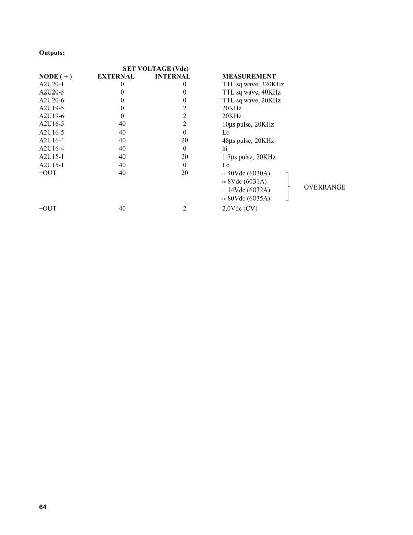
64
Outputs:
SET VOLTAGE (Vdc)NODE ( + ) EXTERNAL INTERNAL MEASUREMENTA2U20-1 0 0 TTL sq wave, 320KHzA2U20-5 0 0 TTL sq wave, 40KHzA2U20-6 0 0 TTL sq wave, 20KHzA2U19-5 0 2 20KHzA2U19-6 0 2 20KHzA2U16-5 40 2 10µs pulse, 20KHzA2U16-5 40 0 LoA2U16-4 40 20 48µs pulse, 20KHzA2U16-4 40 0 hiA2U15-1 40 20 1.7µs pulse, 20KHzA2U15-1 40 0 Lo+OUT 40 20 ≈ 40Vdc (6030A)
≈ 8Vdc (6031A)≈ 14Vdc (6032A)≈ 80Vdc (6035A)
OVERRANGE
+OUT 40 2 2.0Vdc (CV)

65
4Principles of Operation
Introduction
This chapter contains block diagrams, simplified schematics, and related descriptions of the power supply. The instrumentcan be thought of as comprising two major sections: the GPIB, microcomputer, and interface circuitry; and the power meshand control circuits. Block diagrams represent the GPIB board, the front panel board, and the power mesh and controlboard. The descriptions associated with these block diagrams explain the function of each block without describing howindividual components within the circuit accomplish that function. Detailed descriptions are provided only for thoseindividual circuits whose operation may not be obvious to the user.
The circuit names and layouts of the block diagrams are the same as used on the complete schematics; however, some items,such as bias supplies, are left off the block diagrams for clarity. In general, circuits are described as they appear on thediagrams from left to right. Signal names that appear on the drawings are printed in capitals in the descriptions, as arefront-panel labels for indicators and controls. Signal names that describe an operating mode or condition are active whenthat condition exists. For example, OT is high and OT is low if an overtemperature condition exists. Signal flow is from leftto right and top to bottom, unless arrows indicate otherwise.`
The following paragraphs describe the GPIB and the front-panel board. These circuits provide the interface between thepower mesh circuits and the controller and/or operator. The GPIB and front-panel boards are referenced to earth common.Isolation is achieved by optical isolators on the GPIB board. Data is sent between boards serially.
GPIB Board
Circuits on the GPIB board, see Figure 4-1, provide the interface between the power supply and the user, generate thefault/inhibit and relay controls signals (DFI/RI), and supply the analog control and reference signals for the power mesh andreadback circuit. Two microprocessors (primary and secondary) control all data communication between the power supplyand the user. Additional circuits on the GPIB board include the serial interface ports, address switches, an EEPROM, andstatus registers.
Primary Microprocessor
The primary microprocessor controls the GPIB/serial link interface, the front panel data communication, and the DFI/RIinterface. It communicates with the secondary microprocessor through two serial link data lines that are optically coupled toprovide the proper isolation of the user interface from the power mesh. The GPIB board also has a ROM, which containsthe operating firmware, and a RAM, which stores variables such as programmed voltage and current and readback values.
Address Switches
The primary microprocessor determines the GPIB address by reading the address switch settings. Two of the addressswitches determine the power-on SRQ state and the DFI/RI port setting.
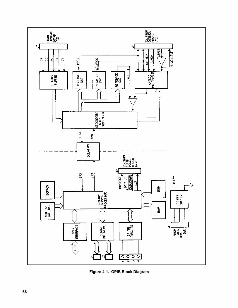
66
Figure 4-1. GPIB Block Diagram
67
EEPROM
The primary microprocessor determines the power supply ID, start-up parameters, calibration constants and scale factors byreading the factory-initialized EEPROM.
Isolation
Two optical isolators transmit serial data between the primary and secondary microprocessors while maintaining electricalisolation between the controller/user-interface and the power mesh.
Secondary Microprocessor
The secondary microprocessor translates the serial data from the primary microprocessor into a parallel data bus and othercontrol signals. Values are loaded into the voltage, current, and readback DAC via the data bus. The secondarymicroprocessor also controls the analog multiplexer, which is used when reading back the actual output.
Digital-to-Analog Converters
Output voltage and current are controlled by two 12-bit DACs whose digital inputs are directly connected to the secondarymicroprocessor. The microprocessor programs the DACs according to data received over the GPIB or from the front panelrotary pulse generator. The DAC circuits also include buffers and compensation amplifiers.
The 12-bit readback DAC is connected to the input of a comparator where it's output is compared to the unknown voltageoutput of the analog multiplexer. The secondary microprocessor programs the output of the readback DAC starting with theMSB and continuing down to the LSB. Each bit is programmed either on or off until the output of the DAC is closest to theunknown voltage output of the multiplexer. At this point, the microprocessor returns the programmed value of the readbackDAC.
Analog Multiplexer
The analog multiplexer selects one of five input voltages to be compared to the readback DAC. This comparison allows themicroprocessor to determine the value of the input voltage. The five inputs of the multiplexer are: CV_PROG andCC_PROG, which are only used during selftest, at power-on, or in response to the TEST? query when the supply isdisabled; OV_MON, which represents the overvoltage trip setting; and I_MON and V_MON, which represent the measuredvalues of output current and voltage.
Status Inputs
The status inputs from the main board provide the following status information to the secondary microprocessor. They are:CC, which is set when the supply is operating in constant current mode; CV, which is set when the supply is in constantvoltage mode; AC_FAULT, which signals that ac power has dropped below the minimum operating voltage of the supply;OT, which indicates an overtemperature condition has occurred on the supply; and OV, which indicates an overvoltage hasoccurred on the supply.
68
Front Panel Board
The front-panel board, see Figure 4-2, contains the VOLTS and AMPS display circuits, the rotary pulse generator (RPG)and RPG decoders, five pushbutton switches, mode indicators, and the OVP ADJUST potentiometer. Data from themicroprocessor is shifted to the display circuits via DATA DOWN , and data from the front-panel controls circuits isshifted to the microprocessor via DATA UP. Circuits on the front-panel board operate from bias voltages supplied from theGPIB board, and are referenced to the same common as the GPIB board (earth ground). The OVP ADJUST potentiometeris part of the power mesh control circuitry (referenced to power supply negative output), and is not connected to any circuitson the front-panel board.
Address Latches and Decoders
DATA DOWN bits received while D / A is low are latched and decoded in this circuit, which then steers clock pulses tothe addressed circuit when D / A goes high.
Volts and Amps Output Ports and Displays
These circuits display values sent by the microprocessor via DATA DOWN. Normally, these are the actual output voltageand current readings. Pressing the DISPLAY SETTINGS switch causes the microprocessor to send the voltage and currentvalues that have been sent by the controller (remote) or RPG (local). If the unit is in CV mode, the voltage display shouldshow the same reading for actual and set values; the current display will switch from the actual value to the current limit. InCC mode, the current readings will be the same and the voltage display will switch from actual value to the voltage limit.Pressing the DISPLAY OVP switch causes the voltage display to show the OVP trip voltage that has been set.
The microprocessor also uses the readout to display the GPIB address switch settings, self test error messages, and readbackoverrange conditions.
RPG and Latches
When rotated, the RPG products two pulse trains that are 90 degrees phase shifted from each other, with the phaserelationship determined by the direction of rotation. This circuit contains two flip-flops that monitor the RPG outputs. Theoutput of one flip-flop goes low to indicate that the RPG has been rotated, and the output of the other goes low to indicateCW rotation or high to indicate CCW rotation. This data is loaded into an input port when D / A is low, and the flip-flopsare set back to their quiescent state by clock pulses from the address decoder when the input port is addressed.
Because the microprocessor reads the input approximately every millisecond, it can determine if the RPG is being turnedrapidly (for a large change) or slowly (for fine adjustment), and the microprocessor varies the rate it changes the DACinputs accordingly.
Front-Panel Switches and Input Port
Five front-panel pushbutton switches plus the two RPG flip-flop outputs are connected to this input port. Data is loadedwhen D / A is low, and is shifted out by clock pulses from the address decoders. The microprocessor reads data in viaDATA UP approximately every millisecond, and checks the switches every 10 ms, thereby ensuring that even rapid switchoperations will be captured.

69
Figure 4-2. Front Panel Block Diagram
70
Mode Indicators
The front-panel mode indicators are controlled by the microprocessor via DATA DOWN and the mode indicator outputports and latches. DATA DOWN signals are shifted in by clock pulses from the address decoders.
OVP Adjust Control
The OVP ADJUST potentiometer sets the voltage level at which the overvoltage protection (OVP) circuit trips.
Power Clear
The power clear signal ( PCLR ) from the GPIB board goes low when the unit is turned on, and remains low until the biaspower supplies have stabilized. This low level resets the display-circuit latches on the front panel board, causing allindicators and display segments to turn on and remain on until the microprocessor updates the display (approximately onesecond).
Power Mesh and Control Board
The basic operating concepts of the power mesh and control circuits are described in the following paragraphs. Thebeginning paragraphs describe the basic difference between an autoranging power supply and a conventional CV/CC powersupply in terms of the available output, and provide an overview of the basic theory of operation. Later paragraphs describethe functions of the individual circuits on the power mesh and control board.
Overview
The basic difference between an autoranging power supply and conventional types of Constant Voltage/Constant Current(CV/CC) power supplies can be seen by comparing the maximum-output-power characteristics of each. A conventionalCV/CC power supply can provide maximum output power at only one combination of output voltage and current, as shownin Figure 4-3a. The range of a power supply can be extended by designing an instrument with two or more switch-selectablevoltage/current ranges within the maximum power-output capability, as shown in Figure 4-3b. An autoranging power supplyprovides maximum output power over a wide and continuous range of voltage and current combinations, as shown in Figure4-3c, without the operator having to select the proper output range.
The unit is a flyback-type switching power supply, so-called from the flyback technique of generating high voltage intelevision receivers. Energy is stored in the magnetic field within a transformer while current flows in the primary, and istransferred to the secondary circuit when current flow in the primary is turned off. Current flow in the primary is controlledby FET switches which are turned on and off at a 20KHz rate by a pulse width modulator. Regulation is accomplished bycontrolling the on time of the FET switches. On pulses are initiated by a clock circuit. Off pulses are initiated when currentflow in the primary has stored enough energy for the output circuit, which is determined as follows.
Sense voltages representing the actual output voltage and current are compared to reference voltages set either byfront-panel controls or remote programming signals. These comparisons produce a control voltage, which represents theamount of power required by the output circuit. Current flow in the primary circuit produces a ramp voltage that representsthe amount of energy being stored for transfer to the output circuit. An off pulse is generated when the ramp voltage exceedsthe control voltage. It can be seen that the power available in the output circuit corresponds to the duty cycle of the FETswitches.
Figure 4-4 shows the relationship of various signals associated with the FET on/off cycle.

71
Figure 4-3. Output Characteristics; Typical, Dual Range, and Autoranging Supplies
Figure 4-4. FET Control Signals Timing Diagram
Power Mesh
Figure 4-5 is a block diagram of the power mesh. These circuits convert the ac input power to approximately 320Vdc, andconvert this dc voltage to the proper dc output voltage.

72
Input Circuits. Primary power is connected through the AC Input Filter to the LINE switch and to the normally opencontacts of the Inrush-Limit relay. When LINE switch is closed, current flows through the inrush current limiting resistorand the normally closed relay contacts to the Bridge Rectifier/Voltage Doubler. This circuit is jumper connected as avoltage doubler for 100 or 115Vac operation and as a full-wave bridge charges to about 320Vdc for any input voltage.Current also flows through the Voltage Select Switch to the Bias Power Supplies, which provide the operating voltages forthe power supply. The Voltage Select Switch connects the primary windings of the bias transformer for operation at 100,120, 220, or 240Vac. The Voltage Select Switch also supplies 120 Vac to the fan and Relay Circuits.
The Inrush Limit relay is energized by RELAY ENABLE , which is generated on the control board after the unit haschecked that various operating voltages are within acceptable limits. After a delay of approximately 2-1/2 seconds, whichallows the Input Filter capacitors to charge, the relay is energized, bypassing the Inrush Limit resistor. A switch on the mainboard switches in more Inrush Limit resistance for 220 or 240Vac operation.
DC To DC Conversion. Current flow from the input rails through the power transformer is controlled by FET switches. Onand off pulses for the FETs are generated on the control board, as will be described shortly. On pulses are applied throughthe On Driver and pulse transformer T1 to the gates of both pairs of FETs. Although the on pulse is only about 1.7µsduration, the FETs' input capacitance holds the FETs on after the on pulse has disappeared.
When the FETs are turned on, current flows through the primaries of Power Transformer T2 and Primary-Current MonitorTransformer T1. The Output Diodes are reverse biased and block current flow in the T2 secondary. Consequently, energy isstored in the field that builds around the T2 transformer windings. The longer that voltage is applied to the primary, themore energy is stored. Current flow in the secondary of T1 is connected to the control board, where it generates a rampvoltage. The amplitude of this linearly increasing voltage corresponds to the amount of current flow through the T2 primary;therefore, it represents the amount of energy being stored in the field around T2. It is this ramp voltage that is compared to acontrol voltage to determine when the FETs should be turned off.
Off pulses turn on Q5 and Q6, which discharge the FET gates, thereby turning the FETs off. When the FETs are turned off,the collapsing magnetic field reverses the polarity across the T2 primary and secondary, and current flows from T2secondary through output diodes to charge the output filter capacitors. The level to which the output capacitors are chargedcorresponds to the length of time that the FETs are on and current flows in T2 primary.
Leakage inductance of T2 attempts to maintain current flow in the primary circuit when the FETs turn off. Flyback diodes inthe FET board protect the FETs by conducting this current around the FETs and back to the input filter.
Down Programmer. This circuit allows the output voltage to be lowered rapidly when required. In order to lower theoutput voltage it is necessary to discharge the output filter capacitors (typically, through the load). In situations that requirethe output voltage to drop more rapidly than can be accomplished through the load, the Down Programmer discharges thecapacitors and pulls the output line low. DOWN PROGRAM ENABLE is generated on the control board. Six conditionscan conditions can trigger down programming: programming of a lower output voltage, overvoltage, overtemperature,remote disable, remote inhibit, or primary power failure.
The + 10.6Vdc bias supply for the Down Programmer stores enough energy in its input capacitor to operate the DownProgrammer after loss of primary power. This ensures that the Down Programmer will be able to discharge the outputcircuit completely when primary power is turned off.
The Agilent 6030A/35A units contain an active bleed circuit, connected across the output, which allows regulation at lowoutput current and/or low output voltage levels. This circuit also minimizes dielectric absorption effects, which show up asnoise on the output of the supply.
Current Monitor Resistor. A highly stable resistance element in the -output line develops the CURRENT SENSE voltage,which is proportional to the power supply output current. This signal is supplied to the CC Circuit on the control board.

73
Control Board
Figure 4-6 is a block diagram of the control board. These circuits monitor the power supply operation and provide thesignals that control the power mesh.
+ 5V Bias Supply. This circuit operates from the + 5V Unregulated voltage from the main board, and generates + 5V and+ 2.5V used by circuits on the control board. Regulated + 5V is also supplied back to the main board for use by the relaycircuits, FET Drivers, and Down Programmer. The + 5V Bias Supply is regulated by a pulse width modulator chip that issynchronized by the 40KHz clock signal to the main Pulse Width Modulator; this eliminates the possibility of frequencymodulated signals on common lines.
Bias Voltage Detector and Relay Driver. The Bias Voltage Detector monitors + 5V Unregulated to determine when biasvoltages are sufficient to ensure proper operation. After turn-on, as the output of the + 5V bias supply rises from 0Vdcthrough approximately 1Vdc, three transistor switches in the Bias Voltage Detector turn on. They inhibit the relay driverand the on-pulse driver, and generate the power-clear signal. The switches remain on until the + 5V Unregulated inputexceeds approximately 13 volts, which is sufficient to ensure both a stable + 5V output and adequate FET drive voltage.
PCLR holds various circuits reset until after the bias voltages stabilize and control circuits are certain to be working.RELAY ENABLE , which is delayed for approximately 2 ½ seconds by the Time Delay Circuit, drives relay circuits on themain board that short out inrush current limiting resistors after input filter capacitors are charged up. RELAY ENABLEcannot occur until bias voltages have stabilized and time delay has expired. ON - PULSE INHIBIT shorts ON pulses toground whenever bias voltage is insufficient to ensure proper operation.
Note that Bias Voltage Detector inhibits power supply operation in two circumstances: while bias voltages are stabilizingafter turn-on, and when ac input drops below an adequate level (brownout).
+ 15V Bias Supply. This circuit produces the + 15V and +5.9V bias voltages. It also produces the reference voltage usedby the CC and CV Current Sources.
Time-Delay Circuit. This circuit generates the signal that delays RELAY ENABLE for approximately 2 ½ seconds aftercessation of an ac fault (Dropout or High AC). The AC FAULT signal is extended for the duration of the time delay andsupplied to: the 1.25KHz counter in the 20KHz Clock Circuit to reset the counter, so that the time delay output of the TimeDelay Circuit will remain set; the Pulse Width Modulator (PWM) to inhibit the PWM in case of an ac fault.
AC Dropout Detector. The AC Dropout Detector operates to shut down the power mesh when primary power is turned offor lost. The circuit monitors the 120Hz signal (full-wave rectified 60 Hz ac) from the bias transformer on the main board.Dropout is detected by a ramp circuit that is reset by the 120 Hz pulses. If the ramp is not reset within approximately 20milliseconds of the previous reset, the circuit generates AC FAULT, which is supplied to the Time Delay Circuit to disableRELAY ENABLE and the PWM.
High AC Detector. The High AC Detector protects the power supply from damage from ac power line surges. The circuitcontains a comparator that monitors the voltage level of the 120Hz signal. If this voltage exceeds a safe operating level, thecircuit generates the HIGH AC signal, which is ORED with AC DROPOUT . Either can cause generation of the ACFAULT signal.
Turn-On Overshoot Control. The Turn-On Overshoot Control Circuit prevents output overshoot when the Pulse WidthModulator is turned back on after having been turned off. The circuit monitors the PWM OFF signal from the Pulse WidthModulator. If the PWM is turned off because of INHIBIT (from GPIB), AC FAULT , OT (overtemperature), or OV(overvoltage), the power supply output will be down programmed to zero, and both the CC and CV Circuit outputs willincrease to maximum in an attempt to restore the output level. This circuit holds the CONTROL PORT at a low level toprevent output overshoot when PWM OFF is removed.

74
Constant Current (CC) Circuit. The Constant Current Circuit compares the CURRENT SENSE voltage level to CCPROGRAMMING VOLTAGE to produce CC CONTROL SIGNAL. CURRENT SENSE is developed across thecurrent-monitor resistor on the main board, and is proportional to the power supply output current. CC PROGRAMMINGVOLTAGE comes from one of a number of sources as selected by the rear-panel mode switches, and represents the desiredoutput current or current limit.
CC CONTROL SIGNAL varies from approximately -1 to +0.5 volts when the power supply is in constant current mode,and is most positive when the CC Circuit is calling for maximum power supply output. CC CONTROL SIGNAL isconnected through an output diode, CR11, shown at the wired-OR gate that is the CONTROL PORT.
The amplified current-sense signal is brought out of the CC Circuit as I-MON (current monitor). I-MON is connected to therear-panel IM terminal, and varies from 0 to + 5 volts as the output current varies from zero to full scale.
A differentiator circuit in the CC Circuit block provides increased stability for highly reactive loads.
Constant Voltage (CV) Circuit. Operation of the CV Circuit is similar to the CC Circuit. The CV Circuit compares theoutput SENSE voltage to the CV PROGRAMMING VOLTAGE to produce the CV CONTROL SIGNAL. + OUT and -OUT are also supplied to the circuit as protection in case the sense leads are inadvertently disconnected. CV CONTROLSIGNAL also varies between approximately -1 to + 0.5 volts, and is connected through diode CR24 to the CONTROLPORT.
The buffered voltage-sense signal is brought out of the CV Circuit as V_MON (voltage monitor). V_MON is connected tothe rear-panel VM terminal, and varies from 0 to + 5 volts as the output voltage varies from zero to full scale. Both V-MONand I-MON are referenced to monitor common ( M).
The CV Circuit also produces the DOWN PROGRAM ENABLE signal when the CV PROGRAMMING VOLTAGE ischanged quickly from a relatively high level to a relatively low level. This allows the power supply output voltage to belowered more rapidly than if the output filter capacitors had to be discharged solely through the load.
CC And CV Current Sources. This circuit generates constant currents that are connected to front-panel VOLTAGE andCURRENT potentiometers of non-- GPIB units to develop the CC and CV programming voltages.
Mode Switches. The rear-panel mode switches select the source of the CC and CV PROGRAMMING VOLTAGES. ForGPIB units, the programming voltages are supplied via the GPIB board, and are connected through mode switches B1 andB4 to the CC and CV Circuits. For non-- GPIB units, mode switches B2, B3, and B5, B6 are closed. The CC and CVCurrent Source outputs are connected through B2 and B5 to the front-panel CURRENT and VOLTAGE potentiometers,and the voltages developed across the potentiometers are connected through B3 and B6 to the CC and CV Circuits.
Remote analog programming voltages can be supplied to the CC and CV Circuits from the rear-panel IP and VP terminals.IP and VP are referenced to program common ( P).
Primary Current Ramp. The output from the primary current-monitor transformer on the main board is developed acrossR116 and R117 to produce a ramp voltage that represents the amount of energy being stored in the power transformer fortransfer to the power supply output circuits. This ramp voltage is connected to the Power Limit Comparator and to theControl Voltage Comparator.
Power Limit Comparator. The power supply maximum output power curve (shown in Specifications Table in theOperating Manual) is defined by this circuit. The PRIMARY CURRENT RAMP voltage, which represents the amount ofpower being supplied to the power supply output, is compared to a voltage which represents the maximum amount of powerthat the power supply can supply safely. If the ramp voltage exceeds the limit voltage, the POWER LIMIT signal isproduced to turn off the PWM.
The Power Limit Comparator Circuit includes a dynamic primary-current-limit circuit, which decreases the primary currentlimit to maintain the output power curve at specified limits.

75
Control Voltage Comparator. This circuit compares the voltage at the CONTROL PORT (represents power required atoutput) with PRIMARY CURRENT RAMP voltage (represents energy being stored for transfer to output). When RAMPvoltage exceeds CONTROL PORT voltage, the Control Voltage Comparator generates the CONTROL LIMIT signal toturn the PWM off. The CONTROL PORT is biased to approximately + 1.3 volts. Whichever control signal, CC or CV, ismore negative (calling for less output power) forward biases its output diode and determines the voltage at the CONTROLPORT.
As can be seen from the waveforms in Figure 4-4, there is a delay between the time when PRIMARY CURRENT RAMPvoltage exceeds the CONTROL PORT voltage and the time when the FETs turn off. This delay consists of the comparatorswitching time, gate delays, transformer delay, and FET turn-off time, and it results in a certain amount of power beingtransferred to the output after the desired off time. If the CONTROL PORT voltage is at a very low level (unit supplyinglittle or no output power), this power may exceed the amount required by the load. To eliminate the delay, the ControlVoltage Comparator includes an initial ramp circuit that generates a small ramp voltage before the FETs are turned on. Theadded ramp voltage starts with the 20KHz clock pulse, and causes the combined-ramp voltage to exceed the CONTROLPORT voltage earlier, thereby effectively eliminating the FET turn-off delay.
Status Drivers. Inputs from the CC and CV Circuits indicate which circuit, if either, is regulating the power supply output.If neither circuit is regulating the output (load calling for more power than the power supply can deliver), logic circuitswithin Status Driver block determine that output is unregulated.
In GPIB units, CC and CV signals go to the microcomputer, which will take appropriate action, including lightingfront-panel indicators. In non-- GPIB units, Status Driver outputs go to front-panel indicators.
20KHz Clock. This circuit contains a 320KHz crystal oscillator and dividers that produce 40KHz, 20KHz, and 1.25KHzsignals. Both the 320KHz and 20KHz signals are supplied to the PWM, with the 20KHz signal controlling the repetitionrate of the PWM.
The 40 KHz signal is supplied to the +5V Bias Supply Circuit to synchronize the PWM in that circuit to the main powersupply PWM. The 1.25KHz output is supplied to the Time Delay Circuit for generating the time delay used to control thepower supply turn-on sequence.
The 1.25KHz signal is subsequently disabled by the AC FAULT output from the Time Delay Circuit at the end of the timedelay.
Pulse Width Modulator (PWM). The PWM generates the ON and OFF pulses that control the power FETs in the powermesh. ON pulses are generated at a 20KHz rate, and, as can be seen in Figure 4-4, are initiated by the first 320KHz dockpulse after the start of the 20KHz clock pulse. When the FET switches turn on, current flows through the Primary CurrentMonitor transformer on the main board, and the Primary CURRENT RAMP voltage starts to rise. OFF pulses are normallyinitiated when CONTROL LIMIT becomes active (low), indicating that the ramp voltage has exceeded the CONTROLPORT voltage. However, an off pulse can be initiated by any one of a number of other signals.
An overtemperature ( OT ), overvoltage ( OV ), remote inhibit, AC FAULT condition or an INHIBIT signal from GPIBwill initiate an OFF pulse, and will also trigger the Down Programmer to reduce output voltage to zero. These conditionswill also cause PWM OFF to be sent to the TurnOn Overshoot Control Circuit.
OFF pulses can also be initiated by POWER LIMIT and by the trailing edge of the 20KHz clock signal. The 20KHz clocksignal ensures that even if nothing else, such as CONTROL LIMIT or POWER LIMIT , initiates an OFF pulse, the FETduty cycle will be limited to less than 50%.
Overvoltage Protection (OVP). The OVP circuit monitors the power supply output voltage and compares it to a presetlimit determined by a front-panel OVP ADJUST potentiometer. If the output voltage exceeds the limit, the OVP Circuitinitiates a PWM OFF pulse, which also triggers the Down Programmer. The OVP Circuit lathes itself until it receives OVCLEAR or ac power is turned off.

76
Figure 4-5. Power Mesh Block Diagram
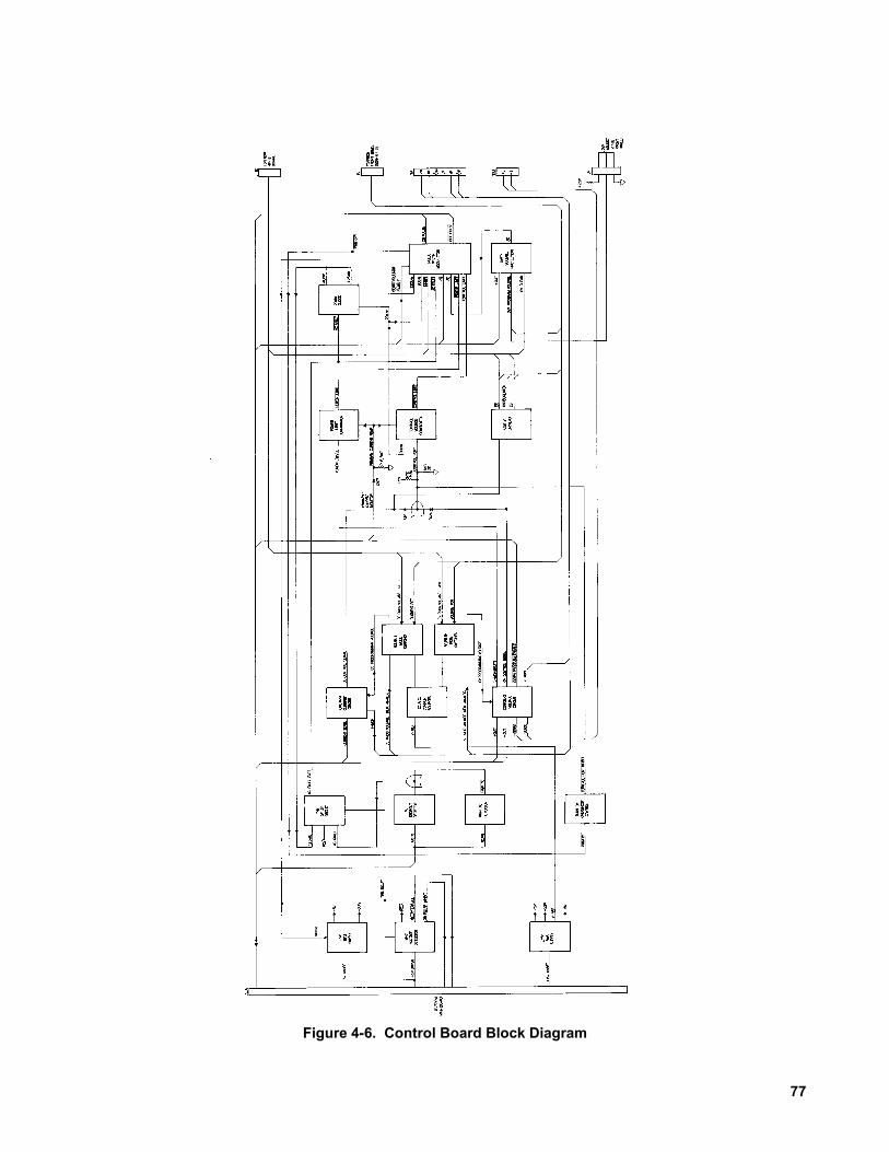
77
Figure 4-6. Control Board Block Diagram

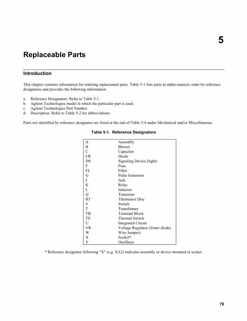
79
5Replaceable Parts
Introduction
This chapter contains information for ordering replacement parts. Table 5-1 lists parts in alpha-numeric order by referencedesignators and provides the following information:
a. Reference Designators. Refer to Table 5-1.b. Agilent Technologies model in which the particular part is used.c. Agilent Technologies Part Number.d. Description. Refer to Table 5-2 for abbreviations.
Parts not identified by reference designator are listed at the end of Table 5-4 under Mechanical and/or Miscellaneous.
Table 5-1. Reference Designators
A AssemblyB BlowerC CapacitorCR DiodeDS Signaling Device (light)F FuseFL FilterG Pulse GeneratorJ JackK RelayL InductorQ TransistorRT Thermistor DiscS SwitchT TransformerTB Terminal BlockTS Thermal SwitchU Integrated CircuitVR Voltage Regulator (Zener diode)W Wire Jumper)X Socket*Y Oscillator
* Reference designator following "X" (e.g. XA2) indicates assembly or device mounted in socket.

80
Ordering Information
To order a replacement part, address order or inquiry to your local Agilent Technologies sales office. Specify the followinginformation for each part: Model, complete serial number, and any Option or special modification (J) numbers of theinstrument; Agilent Technologies part number; circuit reference designator; and description. To order a part not listed inTable 5-4, give a complete description of the part, its function, and its location.
Table 5-2. Description Abbreviations
ADDR AddressableASSY AssemblyAWG American Wire GaugeBUFF BufferCER CeramicCOMP Carbon Film CompositionCONV ConverterDECODER/DEMULTI Decoder/DemultiplexerELECT ElectrolyticEPROM Erasable Programmable Read-Only MemoryFET Field Effect TransistorFF Flip-FlopFXD FixedIC Integrated CircuitINP InputLED Light Emitting DiodeMET MetalizedMOS Metal-Oxide SiliconOP AMP Operational AmplifierOPTO OpticalOVP Over Voltage ProtectionPCB Printed Circuit BoardPORC PorcelainPOS PositivePRIOR PriorityROM Read-Only MemoryRAM Random Access MemoryRECT RectifierREGIS RegisterRES ResistorTBAX Tube AxialTRlG TriggeredUNI UniversalVAR VariableVLTG REG Voltage RegulatorWW Wire Wound

81
Table 5-3. Replaceable Parts List
Ref. Desig Agilent Model Agilent Part Number DescriptionAl 6030A 06030-61032 Main Board Assembly
6031A 06031-61032 "6032A 06032-61032 "6035A 06030-61033 "
Cl,2,4,5,6,8 all 0180-4528 cap 1800µF 200VC9 all 0160-5932 cap 0.47µF 250VC10 6030A,35A 0180-3699 cap 470µF 20% 35V
6031A,32A 0180-0426 cap 22µF 250VC11,12 6030A, 31A 0160-5895 cap 0.047µF
6032A, 35A 0160-5933 cap 0.022µF 10%C13,14 6030A 0180-3702 cap 1600µF 125V
6031A 0180-3425 cap 5500µF 40V6032A* 0180-3492 cap 2600µF 75V6035A 0180-4240 cap 900µF 350V
C15,16 6030A,32A,35A 0180-3587 cap 1000µF 50 V6031A 0180-3425 cap 5500µF 40V
C17,18 6030A,32A,35A 0180-0291 cap lµF 35V6031A 0180-3587 cap 1000µF 50V
C19 6030A* 0160-0269 cap 0.047µF 20%6031A 0180-0291 cap 1µF 35V6032A* 0160-5286 cap 0.47µF 20%6035A* 0180-0904 cap 0.05µF 1KV
C20 6030A,35A* 0160-6392 cap 0.047µF 20%6031A 0180-0291 cap 1µF 35V6032A* 0160-7732 cap 0.47µF
C21 6030A,35A* 0160-6392 cap 0.047µFC22 6030A,35A* 0160-6392 cap 0.047µF 20%
6031A* 0160-5377 cap 2.2µF 10% 63V6032A* 0160-7732 cap 0.47µF
C23 6030A,35A* 0160-6392 cap 0.047µF6031A* 0160-7732 cap 0.47µF
C24 6032A* 0160-4281 cap 2200pF 20%C25 6030A* 0160-0269 cap 0.047µF 20%
6031A* 0160-5377 cap 2.2µF 10% 63V6032A* 0160-5286 cap 0.47µF 20%6035A* 0180-0904 cap 0.05µF 1KV
C26 6031A* 0160-5377 cap 2.2µF 10% 63V6032A* 0160-4281 cap 2200pF 20%
C27 All 0160-6805 cap 0.01µF 400VC27 6031A* 0160-4281 cap 2200pF 20%C28 6031A* 0160-7732 cap 0.47µFC29 6030A,32A,35A 0160-4323 cap 0.047µF 20%, 250V
6031A* 0160-4281 cap 2200pF 20%C30 6030A,32A,35A 0160-7606 cap 1µF 20%C32 6031A 0160-4323 cap 0.047µF 20%, 250VC33 6031A 0160-7606 cap lµF 20%C34 All 0160-6805 cap 0.01µF 400V* Part of output filter, mounted on output bus bars.
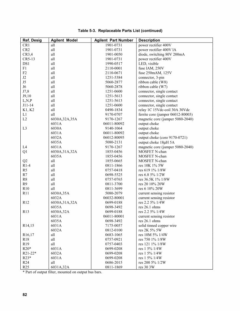
82
Table 5-3. Replaceable Parts List (continued)
Ref. Desig Agilent Model Agilent Part Number DescriptionCR1 all 1901-0731 power rectifier 400VCR2 all 1901-0731 power rectifier 400V lACR3,4 all 1901-0050 diode, switching 80V 200mACR5-13 all 1901-0731 power rectifier 400VDS1 all 1990-0517 LED, visibleF1 all 2110-0001 fuse lAM, 250VF2 all 2110-0671 fuse 250mAM, 125VJ2 all 1251-5384 connector, 3-pinJ5 all 5060-2877 ribbon cable (W8)J6 all 5060-2878 ribbon cable (W7)J7,8 all 1251-0600 connector, single contactJ9,10 all 1251-5613 connector, single contactL,N,P all 1251-5613 connector, single contactJ11-14 all 1251-0600 connector, single contactK1, K2 all 0490-1834 relay 1C 15Vdc-coil 30A 30VdcL1 all 9170-0707 ferrite core (jumper 06012-80003)L2 6030A,32A,35A 9170-1267 magnetic core (jumper 5080-2040)
6031A 06011-80092 output chokeL3 6030A 9140-1064 output choke
6031A 06011-80092 output choke6032A 06012-80095 output choke (core 9170-0721)6035A 5080-2131 output choke 18µH 5A
L4 6031A 9170-1267 magnetic core (jumper 5080-2040)Q1 6030A,31A,32A 1855-0456 MOSFET N-chan
6035A 1855-0456 MOSFET N-chanQ2 all 1855-0665 MOSFET N-chanR1-4 all 0811-1866 res 10K 1% 5WR5 all 0757-0418 res 619 1% 1/8WR7 all 0698-5525 res 6.8 5% 1/2WR8 all 0757-0765 res 36.5K 1% 1/8WR9 all 0811-3700 res 20 10% 20WR10 all 0811-3699 res 6 10% 20WR11 6030A,35A 5080-2079 current sensing resistor
6032A 06032-80001 current sensing resistorR12 6030A,31A,32A 0699-0188 res 2.2 5% 1/4W
6035A 0698-3492 res 26.1 ohmsR13 6030A,32A 0699-0188 res 2.2 5% 1/4W
6031A 06011-80001 current sensing resistor6035A 0698-3492 res 26.1 ohms
R14,15 6031A 7175-0057 solid tinned copper wire6032A 0812-0100 res 2K 5% 5W
R16,17 all 0683-1065 res 10M 5% 1/4WR18 all 0757-0921 res 750 1% 1/8WR19 all 0757-0403 res 121 1% 1/8WR20* 6031A 0699-0208 res 1 5% 1/4WR21-22* 6032A 0699-0208 res 1 5% 1/4WR23* 6031A 0699-0208 res 1 5% 1/4WR24 all 0686-2015 res 200 5% 1/2WR25 6031A,32A 0811-1869 res 30 3W* Part of output filter, mounted on output bus bars.

83
Table 5-3. Replaceable Parts List (continued)
Ref. Desig Agilent Model Agilent Part Number DescriptionR29,30 6030A 0811-1887 res 0.05 5% 10W
6035A 0811-3557 res 0.5 5% 10WR31 6030A 0757-0367 res 100K 1% 1/2W
6035A 0698-8959 res 619K 1% 1/8WR32 6030A 0686-7535 res 75K 5% 1/2W
6035A 0698-8959 res 619K 1% 1/8WR33 6030A 0757-0451 res 24.3K 1% 1/8W
6035A 0757-0471 res 182K 1% 1/8WR34 6030A,35A 0757-0438 res 5.11K 1% 1/8WR35 6030A,35A 0698-8827 res 1M 1% 1/8WR36,37 6030A 0811-1909 res 500 5% 10W
6035A 0811-1913 res 1.5K 5% 10WR38,39 6030A,35A 0757-0467 res 121K 1% 1/8WR41 6030A,35A 0764-0041 res 30 5% 2WR43,44 all 0698-0085 res 2.61k 1% 1/8WR45 all 0698-8827 res 1M 1% 1/8WR46 all 0757-0419 res 681 1% 1/8WR47, 48 all 0698-3622 res 120 5% 2WR49 all 0757-0401 res 100 1% 1/8WS1 all 3101-2046 switch, DPDT slideS2 all 3101-1914 switch, 2-DPDT slideT1 all 9100-4350 current transformerT2 6030A 06030-80090 power transformer
6031A 06011-80090 power transformer6032A 06032-80090 power transformer6035A 9100-4827 power transformer
T3 all 9100-4864 bias transformerU1 all 1906-0389 rectifier bridgeU3 all 1826-0393 IC, voltage regulator 1.2/37VU5 all 1826-0643 IC, voltage regulator 3/30VU6 all 1990-1074 IC, opto-isolatorVR1 all 1902-0955 diode, zener, 7.5VXA4,5 6030A,35A 1252-1052 connector 64-pin
6031A,32A 1251-7891 connector 64-pin
6030A 5060-3520 Output filter board6031A 5060-3524 Output filter board6032A 5060-3523 Output filter board6035A 5060-3521 Output filter board
A1 Mechanicalall 1205-0282 heatsink (U3)all 1205-0862 heatsink (U1)all 2110-0726 fuse clips (F1)all 0403-0086 bumper foot (R9,10)all 0380-1692 standoff, 109mm (4)

84
Table 5-3. Replaceable Parts List (continued)
Ref. Desig Agilent Model Agilent Part Number DescriptionA2 6030A 06030-60022 Control Board Assembly
6031A 06011-60022 "6032A 06032-60022 "6035A 06030-60028 "
C1-4 all 0160-5422 cap 0.047µF 20% 50VC5 all 0160-4801 cap 100pF 5% 100VC6-7 all 0160-5422 cap 0.047µF 20% 50VC8 all 0160-5892 cap 0.22µF 10%C9 all 0160-5422 cap 0.047 20% 50VC10 all 0160-4807 cap 33pF 5% 100VC11 all 0160-5892 cap 0.22µF 10%C12 all 0160-4830 cap 2200pF 10% 100VC13-16 all 0160-5422 cap 0.047µF 20% 50VC17 6030A,32A,35A 0160-4833 cap 0.022µF 10% 100V
6031A 0160-4832 cap 0.01µF 10% 100VC18 all 0160-5892 cap 0.22µF 10%C19 6030A,31A,32A 0160-5469 cap 1µF 10% 50V
6035A 0160-5534 cap 0.1µF 10% 63VC20 6030A,32A,35A 0160-5892 cap 0.22µF 10%
6031A 0160-5534 cap 0.1µF 10% 63VC21,22 all 0160-5422 cap 0.047µF 20% 50VC24 6030A,32A,35A 0160-0162 cap 0.022µF 10% 200V
6031A 0160-0161 cap 0.01µF 10% 200VC25 6030A,32A,35A 0160-4812 cap 220pF 5% 100VC26 all 0160-4807 cap 33pF 5% 100VC27 6030A,32A,35A 0160-5892 cap 0.22µF 10%
6031A 0160-5534 cap 0.1µF 10% 63VC28 6030A,32A,35A 0160-4834 cap 0.047µF 10% 100V
6031A 0160-4833 cap 0.022µF 10% 100VC29 all 0160-5422 cap 0.047µF 20% 50VC30 all 0160-4807 cap 33pF 5% 100VC31 all 0160-5422 cap 0.047µF 20% 50VC32 6030A,32A,35A 0160-5644 cap 0.033µF 10% 50V
6031A 0160-4832 cap 0.01µF 10% 100VC33 6030A 0160-4822 cap 1000pF 5% 100V
6032A 0160-4831 cap 4700pF 10% 100V6035A 0160-4824 cap 680pF 5% 100V
C34 6031A 0160-4832 cap 0.01µF 10% 100V6032A 0160-4835 cap 0.1µF 10% 50V
C35 all 0160-5422 cap 0.047µF 20% 50VC36 all 0160-4812 cap 220pF 5% 100VC37 6032A 0160-4830 cap 2200pF 10% 100VC38-40 all 0160-5422 cap 0.047µF 20% 50VC41 all 0160-4831 cap 4700pF 10% 100VC42 all 0160-4812 cap 220pF 5% 100VC43 all 0160-4831 cap 4700pF 10% 100VC44 all 0160-5422 cap 0.047µ F 20% 50VC45 all 0160-4812 cap 220pF 5% 100VC46 6030A,31A,32A 0160-5166 cap 0.015µF 20% 100V
6035A 0160-4832 cap 0.01µF 20% 100V

85
Table 5-3. Replaceable Parts List (continued)
Ref. Desig Agilent Model Agilent Part Number DescriptionC47 all 0160-5422 cap 0.047µF 20% 50VC48,49 all 0160-4835 cap 0.1µF 10% 50VC50 all 0180-0291 cap 1µF 10% 35VC51 all 0180-1731 cap 4.7µF 50VC52 all 0180-0230 cap 1µF 20% 50VC53 all 0180-1731 cap 4.7µF 50VC54 all 0180-0291 cap 1µF 10% 35VC55 all 0180-0230 cap 1µF 20% 50VC56,57 all 0160-5422 cap 0.047µF 20% 50VC58 all 0160-4801 cap 100pF 5% 100VC59 all 0160-4835 cap 0.1µF 10% 50VC60 all 0160-5422 cap 0.047µF 20% 50VC61 all 0160-4812 cap 220pF 5% 100VC62 all 0160-1835 cap 0.1µF 10% 50VC63 all 0180-1980 cap 1µF 5% 35VC64 all 0180-0116 cap 6.8µ F 10% 35VC65 all 0160-5422 cap 0.047µF 20% 50VC66 all 0160-4801 cap 100pF 5% 100VC67 all 0160-5422 cap 0.047µF 20% 50VC68 all 0160-1822 cap 1000pF 5% 100VC69,70 all 0160-5422 cap 0.047µ F 20% 50VC71 all 0180-0376 cap 0.47µF 10% 35VC72 all 0180-2624 cap 2000µF 10VC73 all 0180-3407 cap 2200µF 35VC74,75 all 0160-5098 cap 0.22µF 10% 50VC76 all 0160-4835 cap 0.1µF 10% 50VC77 all 0160-4833 cap 0.022µF 10% 100VC78 all 0160-4832 cap 0.01µF 10% 100VC79 all 0160-4830 cap 2200pF 10% 100VC80 all 0160-4813 cap 180pF 5% 100VC81 all 0160-5422 cap 0.047µF 20% 50VC82 all 0160-4812 cap 220pF 5% 100VC83 all 0160-5422 cap 0.047µF 20% 50VC84 all 0160-4812 cap 220pF 5% 100VC85 all 0160-4832 cap 0.01µF 10% 100VCR1-6 all 1901-0033 gen prp 180V 200mACR7,8 all 1901-0050 switching 80V 200mACR9,10 all 1901-0033 gen prp 180V 200mACR11 all 1901-0050 switching 80V 200mACR12 all 1901-0033 gen prp 180V 200mACR13,14 all 1901-0050 switching 80V 200mACR15,16 all 1901-0033 gen prp 180V 200mACR17,18 all 1901-0050 switching 80V 200mACR19 all 1901-0033 gen prp 180V 200mACR20-31 all 1901-0050 switching 80V 200mACR32 all 1901-0992 schottky 40V 3AJ1,2 all 1251-8417 connector 16-pinJ3 6030A,35A 1251-7743 connector 26-pin
6031A,32A 1251-5927 connector 26-pinJ4 all 1251-8676 connector 5-pin

86
Table 5-3. Replaceable Parts List (continued)
Ref. Desig Agilent Model Agilent Part Number DescriptionJ5,6 all 1251-5240 connector 20-pinJ15 6030A,35A 1251-0600 connector 1-pinL1 all 06023-80090 chokeQ1-3 all 1854-0823 transistor NPN SiQ4-6 all 1855-0413 J-FET P-chan SiQ7 all 1854-0823 transistor NPN SiQ8 all 1853-0012 transistor PNP SiQ9 all 1854-0635 transistor NPN SiQ10 all 1853-0036 transistor PNP SiQ11 all 1858-0023 transistor arrayR1,2 all 0686-5125 res 5.1K 5% 1/2WR3 all 0683-5125 res 5.1K 5% 1/4WR4 all 0757-0483 res 562K 1% 1/8WR5 all 0683-2015 res 200 5% 1/4WR6 6030A 0698-6615 res 3.75K 0.1%
6031A 0699-1011 res 3.32K 1% 1/8W6032A 0698-7631 res 2.87K 1%6035A 0757-0424 res 1.1K 1% 1/8W
R7 all 0683-5125 res 5.1K 5% 1/4WR8 all 2100-3353 trimmer 20K 10%R9 6030A,31A,32A 2100-3352 trimmer lK 10%
6035A 2100-3351 trimmer 500 10%R10 all 0698-3433 res 28.7 1% 1/8WR11,12 6030A,32A,35A 0757-0465 res 100K 1% 1/8WR13 6030A,35A 0698-3430 res 21.5 1% 1/8W
6032A 0757-0379 res 12.1 1% 1/8WR14,15 all 0686-5125 res 5.1K 1/2WR16 all 0683-2015 res 200 5% 1/4WR17 all 0698-7082 res 100K 1% 1/8WR18 all 0683-1025 res 1K 5% 1/4WR19 all 0757-0442 res 10K 1% 1/8WR20 6030A,35A 0686-5135 res 51K 5% 1/2W
6031A,32A 0686-1025 res 1K 5% 1/4WR21 6030A,35A 2100-3274 trimmer 10K 10%
6031A 2100-3350 trimmer 200 10%6032A 2100-3273 trimmer 2K 10%
R22 all 2100-3353 trimmer 20K 10%R23 all 2100-3273 trimmer 2K 10%R24 all 2100-3350 trimmer 200 10%R25 all 2100-3273 trimmer 2K 10%R26 all 2100-3274 trimmer 10K 10%R27 all 0757-0470 res 162K 1% 1/8WR28 all 0757-0464 res 90.9K 1% 1/8WR29 all 0698-4509 res 80.6K 1% 1/8WR30 all 0757-0280 res 1K 1% 1/8WR31 6030A,31A,32A 0698-3260 res 464K 1% 1/8W
6035A 0757-0741 res 182K 1% 1/8WR32 all 0698-8827 res 1M 1% 1/8WR33 all 0698-3449 res 28.7K 1% 1/8WR34 6030A,32A,35A 0757-0458 res 51.1K 1% 1/8W

87
Table 5-3. Replaceable Parts List (continued)
Ref. Desig Agilent Model Agilent Part Number Description6031A 0757-0442 res 10K 1% 1/8W
R35 6030A,35A 0683-1055 res 1M 5% 1/4W6031A 0683-3355 res 3.3M 5% 1/4W6032A 0683-1555 res 1.5M 5% 1/4W
R36 all 0698-3455 res 261K 1% 1/8WR37 all 0698-4536 res 340K 1% 1/8WR38 6030A,35A 0698-4536 res 340K 1% 1/8W
6031A,32A 0698-3455 res 261K 1% 1/8WR39 all 0683-4725 res 4.7K 5% 1/4WR40 6030A,32A 0699-1210 res 80K 0.1% 0.1W
6035A6035A
0698-69790683-2055
res 111.1K 1%res 2M 1% assembled
in parallelR41 6030A 0699-1744 res 280K 1% 0.1W
6031A 0699-0118 res 20K 0.1% 0.1W6032A 0699-1210 res 80K 0.1% 0.1W6035A 0699-3104 res 250K 0.1% 0.1W
R42 6030A,35A 0699-1742 res 70K 0.1% 0.1W6031A 0699-0059 res 5K 0.1% 0.1W6032A 0699-0642 res 10K 0.1% 0.1W
R43 6030A,35A 0699-1743 res 345K 0.1% 0.1W6031A 0699-0118 res 20K 0.1% 0.1W6032A 0699-1211 res 95K 0.1% 0.1W
R44 all 0757-0199 res 21.5K 1% 1/8WR45 all 0698-8816 res 2.15 1% 1/8WR46 6030A,32A,35A 0683-1255 res 1.2M 5% 1/4W
6031A 0698-4539 res 402K 1% 1/8WR47 6030A,32A,35A 0757-0470 res 162K 1% 1/8W
6031A 0757-0458 res 51.1K 1%R48 all 0757-0458 res 51.1K 1%R49 6030A 0699-1745 res 560K 0.1% 1/4W
6031A 7175-0057 jumper6032A 0698-7496 res 20K 0.1% 1/4W6035A 0698-6369 2 - resistors 1M 1% (assembled in series )
R50 6030A,35A 0686-5135 res 51K 5% 1/2W6031A,32A 0686-1025 res 1K 5% 1/2W
R51 6030A,32A,35A 7175-0057 jumper6031A 0698-3433 res 28.7 1% 1/8W
R52 6030A,35A 0699-1742 res 70K 0.1% 0.1W6031A 0699-0059 res 5K 0.1% 0.1W6032A 0699-0642 res 10K 0.1% 0.1W
R53 6030A,35A 0757-0451 res 24.3K 1% 1/8W6031A 0757-0462 res 75K 1% 1/8W6032A 0757-0458 res 51.1K 1% 1/8W
R54 all 0698-3450 res 42.2K 1% 1/8WR55 6030A,35A 0757-0451 res 24.3K 1% 1/8W
6031A 0757-0462 res 75K 1% 1/8W6032A 0757-0458 res 51.1K 1% 1/8W
R56 6030A,32A,35A 0757-0199 res 21.5K 1% 1/8W6031A 7175-0057 jumper
R57 6030A,31A,32A 0698-3155 res 4.64K 1% 1/8W

88
Table 5-3. Replaceable Parts List (continued)
Ref. Desig Agilent Model Agilent Part Number DescriptionR57 6035A 0757-0124 res 39.2K 1% 1/8WR58 6030A 0757-0344 res 1M 1% 1/4W
6031A 0757-0449 res 20K 1% 1/8W6032A 0698-3572 res 60.4K 1% 1/8W6035A 0699-1630 res 4M 0.25% 1/2W
R59,60 6030A 0698-4486 res 24.9K 1% 1/8W6031A 0757-0442 res 10K 1% 1/8W6032A 0757-0438 res 5.11K 1% 1/8W6035A 0698-7668 res 39.91K 1%
R61 6030A 0757-0344 res 1M 1% 1/4W6031A 0757-0449 res 20K 1% 1/8W6032A 0698-3572 res 60.4K 1% 1/8W6035A 0699-1630 res 4M 0.25% 1/2W
R62 all 0757-0124 res 39.2K 1% 1/8WR63 all 0683-1015 res 100 5% 1/4WR64 6030A,32A,35A 0757-0124 res 39.2K 1% 1/8W
6031A 0757-0270 res 249K 1% 1/8WR65 6032A 0757-0473 res 221K 1% 1/8WR66 all 0683-4725 res 4.7K 5% 1/4WR67 6031A 0757-0459 res 56.2K 1% 1/8W
6032A 0757-0123 res 34.8K 1% 1/8WR68 all 0757-0270 res 249K 1% 1/8WR69 all 0683-1015 res 100 5% 1/4WR70 all 0757-0449 res 20K 1% 1/8WR71 all 0698-0085 res 2.61K 1% 1/8WR72 all 0757-0452 res 27.4K 1% 1/8WR73 6030A,35A 0757-0289 res 13.3K 1% 1/8W
6031A 0757-0442 res 10K 1% 1/8W6032A 0757-0461 res 68.1K 1% 1/8W
R74 all 0757-0460 res 61.9K 1% 1/8WR75 all 0698-8827 res 1M 1% 1/8WR76 all 0757-0438 res 5.11K 1% 1/8WR77 all 0683-4715 res 470 5% 1/4WR78 all 0698-6322 res 4K 1% 1/8WR79,80 all 0683-2035 res 20K 5% 1/4WR81 6030A,32A,35A 0757-0419 res 681 1% 1/8W
6031A 0698-3444 res 316 1% 1/8WR82 all 0683-4715 res 470 5% 1/4WR83 all 0698-6322 res 4K 1% 1/8WR84 all 0698-6320 res 5K 0.1% 1/8WR85 all 0698-6983 res 20.4K 0.1% 1/8WR86 all 0757-0465 res 100K 1% 1/8WR87 6030A 0699-1741 res 5.657K 0.1% 1/8W
6031A 0698-6322 res 4K 1% 1/8W6032A 0698-7933 res 3.83K 0.1% 1/8W6035A 0699-2850 res 10.04K 0.1%
R88 6030A 0699-1745 res 500 0.1% 1/8W6031A 0698-8695 res 36K 0.1% 1/8W6032A 0698-6979 res 111.1K 01% 1/8W6035A 0698-6950 2 - resistors 1.25M .1% (assembled in series )

89
Table 5-3. Replaceable Parts List (continued)
Ref. Desig Agilent Model Agilent Part Number DescriptionR89-91 all 0683-2225 res 2.2K 5% 1/4WR92 6030A,35A 0898-4480 res 15.8K 1% 1/8W
6031A 0757-0457 res 47.5K 1% 1/8W6032A 0757-0464 res 90.9K 1% 1/8W
R93 all 0683-3325 res 3.3K 5% 1/4WR94,95 all 0683-2225 res 2.2K 5% 1/4WR96 all 0757-0481 res 475K 1% 1/8WR97 all 0757-0290 res 6.19K 1% 1/8WR98 all 0757-0444 res 12.1K 1% 1/8WR99 all 0698-4416 res 169 1% 1/8WR100 all 0757-0404 res 130 1% 1/8WR101 all 0698-4608 res 806 1% 1/4WR102 all 0698-4447 res 280 1% 1/8WR103 all 0698-4416 res 169 1% 1/8WR104,105 all 0683-4725 res 4.7K 5% 1/4WR106 6030A,35A 0757-0404 res 130 5% 1/4W
6031A,32A 0683-2715 res 270 5% 1/4WR107 6030A,35A 0757-0404 res 130 5% 1/4W
6031A,32A 0683-1815 res 180 5% 1/4WR108 6030A,35A 0757-0404 res 130 5% 1/4W
6031A,32A 0683-2715 res 270 5% 1/4WR109 6030A,35A 0757-0404 res 130 5% 1/4W
6031A,32A 0683-1815 res 180 5% 1/4WR110 all 0683-5105 res 51 5% 1/4WR111 all 0683-2035 res 20K 5% 1/4WR112 all 0757-0199 res 21.5K 1% 1/8WR113 all 0757-0283 res 2K 1% 1/8WR114 all 0683-2225 res 2.2K 5% 1/4WR115 all 0757-0280 res 1K 1% 1/8WR116,117 all 0757-0346 res 10 1% 1/8WR118 all 0698-3498 res 8.66K 1% 1/8WR119 all 0757-0438 res 5.11K 1% 1/8WR120 all 0683-4725 res 4.7K 5% 1/4WR121 all 0683-2025 res 2K 5% 1/4WR122 all 0683-1025 res 1K 5% 1/4WR123 all 0683-4715 res 470 5% 1/4WR124 all 0757-0442 res 10K 1% 1/8WR125 all 0757-0465 res 100K 1% 1/8WR126 all 0757-0442 res 10K 1% 1/8WR127 all 0698-8827 res 1M 1% 1/8WR128 all 0698-3136 res 17.8K 1% 1/8WR129 all 0698-4121 res 11.3K 1% 1/8WR131 all 0757-0449 res 20K 1% 1/8WR132 all 1810-0205 network, sip 4.7K X7R133 all 0683-5625 res 5.6K 5% 1/4WR134 all 0683-1025 res 1K 5% 1/4WR135 all 0683-1855 res 1.8M 5% 1/4WR136 all 0757-0420 res 750 1% 1/4WR137 all 0698-4435 res 2.49K 1% 1/8WR138 all 0757-0199 res 21.5K 1% 1/8W
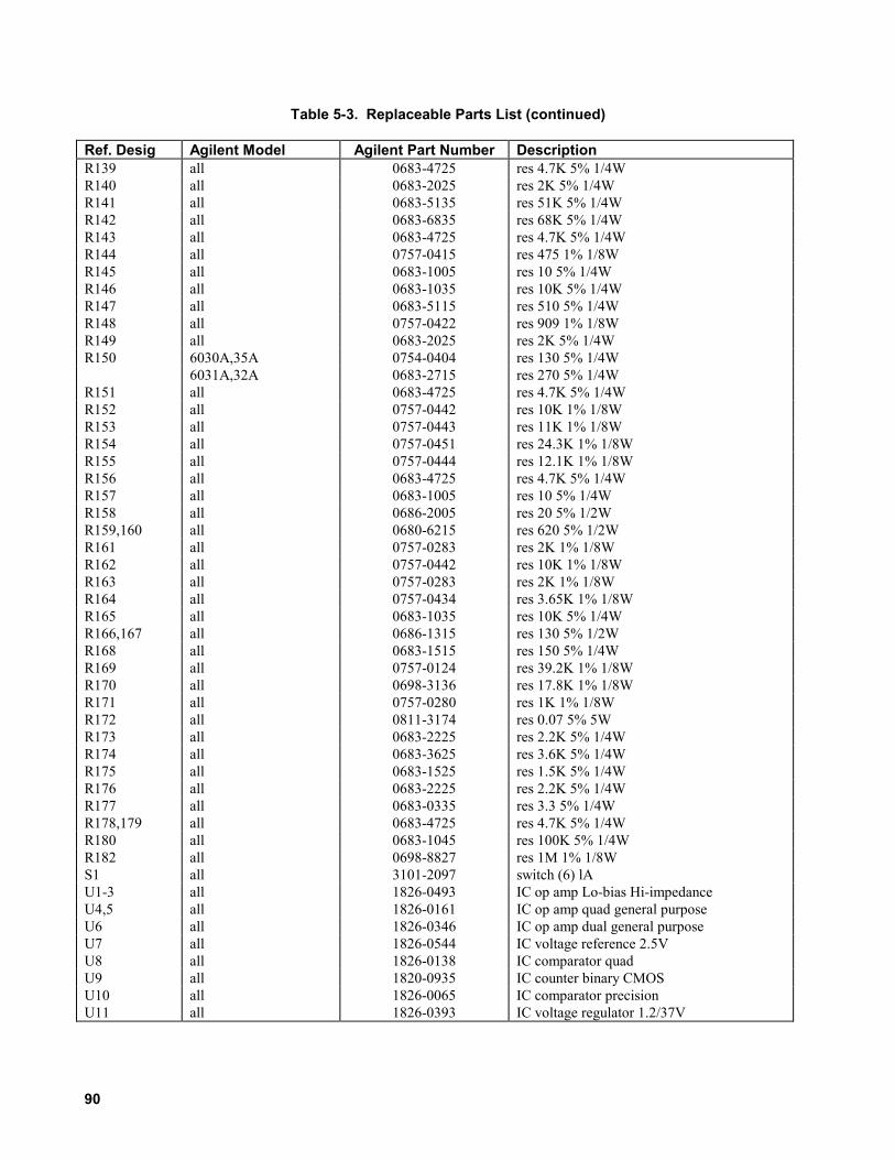
90
Table 5-3. Replaceable Parts List (continued)
Ref. Desig Agilent Model Agilent Part Number DescriptionR139 all 0683-4725 res 4.7K 5% 1/4WR140 all 0683-2025 res 2K 5% 1/4WR141 all 0683-5135 res 51K 5% 1/4WR142 all 0683-6835 res 68K 5% 1/4WR143 all 0683-4725 res 4.7K 5% 1/4WR144 all 0757-0415 res 475 1% 1/8WR145 all 0683-1005 res 10 5% 1/4WR146 all 0683-1035 res 10K 5% 1/4WR147 all 0683-5115 res 510 5% 1/4WR148 all 0757-0422 res 909 1% 1/8WR149 all 0683-2025 res 2K 5% 1/4WR150 6030A,35A 0754-0404 res 130 5% 1/4W
6031A,32A 0683-2715 res 270 5% 1/4WR151 all 0683-4725 res 4.7K 5% 1/4WR152 all 0757-0442 res 10K 1% 1/8WR153 all 0757-0443 res 11K 1% 1/8WR154 all 0757-0451 res 24.3K 1% 1/8WR155 all 0757-0444 res 12.1K 1% 1/8WR156 all 0683-4725 res 4.7K 5% 1/4WR157 all 0683-1005 res 10 5% 1/4WR158 all 0686-2005 res 20 5% 1/2WR159,160 all 0680-6215 res 620 5% 1/2WR161 all 0757-0283 res 2K 1% 1/8WR162 all 0757-0442 res 10K 1% 1/8WR163 all 0757-0283 res 2K 1% 1/8WR164 all 0757-0434 res 3.65K 1% 1/8WR165 all 0683-1035 res 10K 5% 1/4WR166,167 all 0686-1315 res 130 5% 1/2WR168 all 0683-1515 res 150 5% 1/4WR169 all 0757-0124 res 39.2K 1% 1/8WR170 all 0698-3136 res 17.8K 1% 1/8WR171 all 0757-0280 res 1K 1% 1/8WR172 all 0811-3174 res 0.07 5% 5WR173 all 0683-2225 res 2.2K 5% 1/4WR174 all 0683-3625 res 3.6K 5% 1/4WR175 all 0683-1525 res 1.5K 5% 1/4WR176 all 0683-2225 res 2.2K 5% 1/4WR177 all 0683-0335 res 3.3 5% 1/4WR178,179 all 0683-4725 res 4.7K 5% 1/4WR180 all 0683-1045 res 100K 5% 1/4WR182 all 0698-8827 res 1M 1% 1/8WS1 all 3101-2097 switch (6) lAU1-3 all 1826-0493 IC op amp Lo-bias Hi-impedanceU4,5 all 1826-0161 IC op amp quad general purposeU6 all 1826-0346 IC op amp dual general purposeU7 all 1826-0544 IC voltage reference 2.5VU8 all 1826-0138 IC comparator quadU9 all 1820-0935 IC counter binary CMOSU10 all 1826-0065 IC comparator precisionU11 all 1826-0393 IC voltage regulator 1.2/37V

91
Table 5-3. Replaceable Parts List (continued)
Ref. Desig Agilent Model Agilent Part Number DescriptionU12 all 1826-0527 IC voltage regulator 1.2/37VU13 all 1820-1287 IC buffer quad NANDU15 all 1820-1272 IC buffer quad NORU16 all 1820-1437 IC multivibrator monostable dualU17 all 1826-0138 IC comparator quadU18 all 1820-1205 IC gate dual ANDU19 all 1820-1112 IC flip flop D-typeU20 all 1820-2096 IC counter binary dualU21 all 1826-0544 IC voltage reference 2.5VU22 all 1826-0428 IC voltage regulator 1/40VU23 all 1826-0065 IC comparator precisionVR1 all 1902-3110 diode, zener 5.9V 2%VR2 all 1902-0777 diode, zener 6.2VVR3,4 all 1902-0018 diode, zener 11.7VVR5 all 1902-0575 diode, zener 6.5V 2%VR6 all 7175-0057 jumperW1-3 all 7175-0057 jumperY1 all 0960-0586 resonator, ceramic
A2 Mechanicalall 1205-0282 heat sink (Q9, U11, U12)all 1200-0485 IC socket (S1)all 1200-0181 insulator, (Q8)all 0360-2195 terminal block, 6-positionall 0360-2192 terminal block, 2-position
A3 all 06031-60020 Front Panel BoardC1-4 all 0160-5422 cap 0.047µF 20% 50VC5 all 0180-0374 cap 10µF 20%C6-9 all 0160-5422 cap 0.047µF 20% 50VC10 all 0180-0374 cap 10µF 20%C11-13 all 0160-5422 cap 0.047µF 20% 50VDS1-6 all 1990-0835 LEDDS7-12 all 1990-0831 LEDDS13-15 all 1990-0835 LEDDS16-23 all 1990-0985 display-kitG1 all 06032-60006 rotary pulse generatorJ1 all 1251-8417 connector 16-pinJ2,3 all 1251-8675 connector 5-pinL1 all 9100-1618 coil 5.6µH 10%R1 all 1810-0272 network, sip 330 X9R2 all 0683-2225 res 2.2K 5% 1/4WR3-5 all 0683-3315 res 330 5% 1/4WR6-38 all 0683-4715 res 470 5% 1/4WR40-64 all 0683-4715 res 470 5% 1/4WR65-68 all 0683-2225 res 2.2K 5% 1/4WR69-71 all 0683-3315 res 330 5% 1/4WR72 all 2100-1775 trimmer 5K 5%R73 all 0683-1015 res 100 5% 1/4WS1-5 all 5060-9436 switch, lighted pushbutton

92
Table 5-3. Replaceable Parts List (continued)
Ref. Desig Agilent Model Agilent Part Number DescriptionU1-4, 6-11 all 1820-1433 IC shift register, 8-bitU5 all 1820-1216 IC decoder, 3-to-8 lineU12 all 1820-1216 IC decoder, 3-to-8 lineU13 all 1820-1112 IC flip flop, D-typeU14 all 1820-1199 IC inverter, HEXU15 all 1820-1197 IC gate quad NANDU16 all 1820-1433 IC shift register, 8-bitU17 all 1820-1975 IC shift register, 8-bit
A3 Mechanicalall 4040-1615 stand off (DS1-15)
A4 all 06011-60023 FET BoardC1 all 0160-4569 cap 0.01µF 10% 800VdcC2 all 0160-5981 cap 0.047µF 10% 630VdcC3 all 0160-4569 cap 0.01µF 10% 800VdcC4 all 0160-5981 cap 0.047µF 10% 630VdcC5,6 all 0160-4835 cap 0.1µF 10% 50VC7 all 0180-0116 cap 6.8µF 10% 35VC8 all 0180-0228 cap 22µF 10% 15VCR1 all 1901-1418 power rectifier 600VCR2,3 all 1901-1087 power rectifier 600VCR4 all 1901-1418 power rectifier 600VCR5-11 all 1901-0050 diode, switching 80V 200mAF1,2 all 2110-0671 fuse 125mAM, 125VL14 all 9100-1610 coil 0.15µH 20%P1 all 1252-1053 connector 64-pinQ1-4 all 1855-0473 FET N-channelQ5,6 all 1854-0585 transistor NPN SiR1-4 all 0811-1065 res 150 5% 10WR5-8 all 0698-3609 res 22 5% 2WR9-11 all 0698-5139 res 3.9 5% 5WR12 all 0757-0466 res 110K 1% 1/8WR13-16 all 0698-3609 res 22 5% 2WR17-19 all 0698-5139 res 3.9 5% 0.5WR20 all 0757-0379 res 12.1 1% 1/8WR21 all 0683-1505 res 15 5% 1/4WR22 all 0683-1815 res 180 5% 1/4WR23,24 all 0686-2005 res 20 5% 1/2WR25 all 0757-0466 res 110K 1% 1/8WR26 all 0683-1815 res 180 5% 1/4WR27 all 0757-0379 res 12.1 1% 1/8WR28 all 0683-1505 res 15 5% 1/4 WR29-33 all 0683-0475 res 4.7 5% 1/4WR34 all 0683-0275 res 2.7 5% 1/4WTS1 all 3103-0081 switch, thermal +202FT1 all 06011-80091 transformerT2 all 06011-80095 transformerU1-3 all 1820-1050 IC driver dual NORVR1,2 all 1902-0779 diode, zener 11.8V 5%

93
Table 5-3. Replaceable Parts List (continued)
Ref. Desig Agilent Model Agilent Part Number DescriptionA4 Mechanical
all 1205-0398 heatsink (CR1,4)all 1252-0093 socket pin (Q1-4) (8)all 06032-20001 heatsink (Q1,Q2)all 06032-20002 heatsink (Q3,Q4)all 0380-1524 standoff, hex (7)
A5 6030A 06030-60024 Diode Board6031A 06011-60024 "6032A 06032-60029 "6035A 06030-60029 "
C1 6030A,32A,35A 0180-3167 cap 1000µF 20% 25V6031A 0160-4832 cap 0.01µF 10% 100V
C2 6030A 0160-5464 cap 0.01µF 5% 1.5KVdc6031A 0160-5422 cap 0.047µF 20% 50V6032A 0160-4569 cap 0.01µF 10% 800Vdc6035A 0160-7222 cap 0.0022µF 10% 1600Vdc
C3 6030A,32A,35A 0160-5422 cap 0.047µF 20% 50Vdc6031A 0180-3167 cap 1000µF 25V
C4 6030A,32A 0160-4832 cap 0.01µF 10% 100Vdc6031A 0160-6077 cap 0.015µF 200V6035A 0160-4835 cap 0.1µF 10% 50V
C5 6030A 0160-5464 cap 0.01µF 5% 1.5KVdc6031A 0160-6077 cap 0.015µF 200V6035A 0160-7222 cap 0.0022µF 10% 1600Vdc
C7 6035A 0160-5166 cap 0.015µF 10% 100VdcCR1 6030A,32A,35A 1901-0050 diode, switching 80V 200ma
6031A 1901-1127 power rectifier 150V 70ACR2 6030A,32A,35A 1901-0731 power rectifier 400V lA
6031A 1901-0050 diode, switching 80V 200maCR3 all 1901-0050 diode, switching 80V 200mACR4 6030A 1901-1542 power rectifier 400V 50A
6031A 1901-0731 power rectifier 400V lA6032A 1901-0887 power rectifier 300V 50A6035A 1901-1388 power rectifier lKV 40A
CR5 6030A 1901-1542 power rectifier 400V 50A6031A 1901-1127 power rectifier 150V 70A6035A 1901-1388 power rectifier lKV 40A
CR6 6030A,35A 1902-3203 diode, zener 14.7V 5%F1 6031A,32A 2110-0546 fuse 5AM, 125VL1 6030A 9170-1334 ferrite core (jumper 5080-2065)
6031A 06011-80003 ferrite core (jumper 8150-4777)6032A 9170-0707 ferrite core (jumper 06012-80003)6035A 5080-2132 inductor L2
L2 6030A 9170-1334 ferrite core (jumper 5080-2065)6031A 06011-80003 ferrite core (jumper 8150-4777)6035A 5080-2132 inductor
L3 6030A, 35A 9170-0894 core shield bead (ref Q1)P1 all 1252-1053 connector 64-pin

94
Table 5-3. Replaceable Parts List (continued)
Ref. Desig Agilent Model Agilent Part Number DescriptionQ1 6030A, 35A 1855-0767 FET N-channel
6031A 1854-0264 transistor NPN, Si6032A 1855-0549 FET N-channel
Q2 6031A 1855-0549 FET N-channel6032A 1854-0755 transistor NPN Si
R1 6030A,32A,35A 0683-1855 res 1.8M 5% 1/4W6031A 0811-3460 res 0.05 5% 5W
R2 6030A,32A,35A 0698-3151 res 2.87K 1% 1/8W6031A 0686-1005 res 10 5% 1/2W
R3 6030A,32A,35A 0757-0459 res 56.2K 1% 1/8W6031A 0683-1025 res 1K 5% 1/8 W
R4 6030A,32A,35A 0698-3202 res 1.74K 1% 1/8W6031A 0757-0317 res 1.33K 1% 1/8W
R5 6030A,32A,35A 0757-0317 res 1.33K 1% 1/8W6031A 0698-4196 res 1.07K 1% 1/8W
R6 6030A,32A,35A 0683-1045 res 100K 5% 1/4W6031A 0698-4211 res 158K 1% 1/8W
R7 6030A, 35A 0683-2735 res 26K 5% 1/4W6031A 0757-0465 res 100K 1% 1/8W6032A 0683-1025 res 1K 5% 1/4W
R8 6030A,32A,35A 0698-7332 res 1M 1% 1/8W6031A 0757-0447 res 16.2K 1% 1/8W
R9 6030A 0698-8144 res 787K 1% 1/8W6031A 0757-0428 res 1.62K 1% 1/8W6032A 0757-0480 res 432K 1% 1/8W6035A 0683-2055 res 2M 5%
R10 6030A, 35A 0698-3512 res 1.8K 1% 1/8W6031A 0698-3601 res 10 5% 2W6032A 0698-4196 res 1.07K 1% 1/8 W
R11 6031A 0698-3601 res 10 5% 2W6032A 0686-1005 res 10 5% 1/2W
R12 6030A, 32A, 35A 0757-0447 res 16.2K 1% 1/8W6031A 0698-3609 res 22 55% 2W
R13 6030A, 32A, 35A 0683-1005 res 10 5% 1/4W6031A 0698-3609 res 22 55% 2W
R14 6030A 0811-1746 res 0.36 5% 2W6031A 0757-0459 res 56.2K 1% 1/8W6032A 0811-3290 res 0.1 5% 2W6035A 0811-0923 res 0.91 5% 2W
R15 6030A 0811-3729 res 250 5% 10W6031A 0683-1855 res 1.8M 5% 1/4W6032A 0811-1068 res 50 5% 10W6035A 0811-3842 res 600 10% 10W
R16 6030A 0811-3729 res 250 5% 10W6031A 0698-7332 res 1M 1% 1/8W6035A 0811-3842 res 600 10% 10W
R17 6030A 0811-3729 res 250 5% 10W6031A 0698-4444 res 4.87K 1% 1/8W6035A 0811-3842 res 600 10% 10W
R18 6030A 0811-3729 res 250 5% 10W
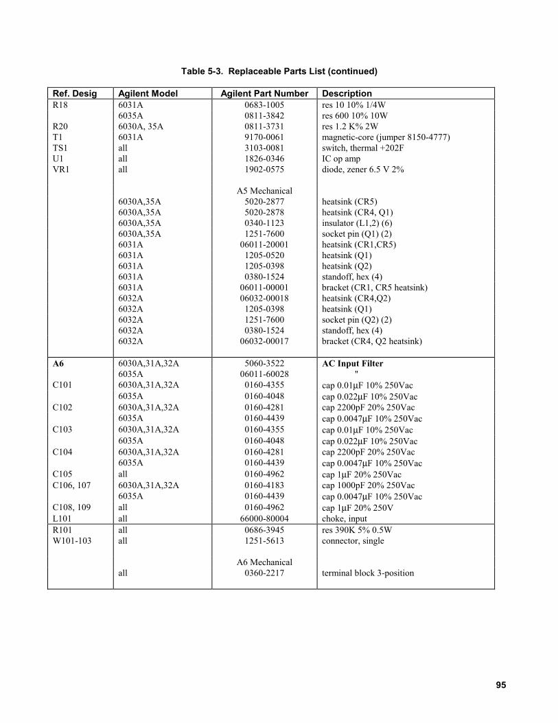
95
Table 5-3. Replaceable Parts List (continued)
Ref. Desig Agilent Model Agilent Part Number DescriptionR18 6031A 0683-1005 res 10 10% 1/4W
6035A 0811-3842 res 600 10% 10WR20 6030A, 35A 0811-3731 res 1.2 K% 2WT1 6031A 9170-0061 magnetic-core (jumper 8150-4777)TS1 all 3103-0081 switch, thermal +202FU1 all 1826-0346 IC op ampVR1 all 1902-0575 diode, zener 6.5 V 2%
A5 Mechanical6030A,35A 5020-2877 heatsink (CR5)6030A,35A 5020-2878 heatsink (CR4, Q1)6030A,35A 0340-1123 insulator (L1,2) (6)6030A,35A 1251-7600 socket pin (Q1) (2)6031A 06011-20001 heatsink (CR1,CR5)6031A 1205-0520 heatsink (Q1)6031A 1205-0398 heatsink (Q2)6031A 0380-1524 standoff, hex (4)6031A 06011-00001 bracket (CR1, CR5 heatsink)6032A 06032-00018 heatsink (CR4,Q2)6032A 1205-0398 heatsink (Q1)6032A 1251-7600 socket pin (Q2) (2)6032A 0380-1524 standoff, hex (4)6032A 06032-00017 bracket (CR4, Q2 heatsink)
A6 6030A,31A,32A 5060-3522 AC Input Filter6035A 06011-60028 ''
C101 6030A,31A,32A 0160-4355 cap 0.01µF 10% 250Vac6035A 0160-4048 cap 0.022µF 10% 250Vac
C102 6030A,31A,32A 0160-4281 cap 2200pF 20% 250Vac6035A 0160-4439 cap 0.0047µF 10% 250Vac
C103 6030A,31A,32A 0160-4355 cap 0.01µF 10% 250Vac6035A 0160-4048 cap 0.022µF 10% 250Vac
C104 6030A,31A,32A 0160-4281 cap 2200pF 20% 250Vac6035A 0160-4439 cap 0.0047µF 10% 250Vac
C105 all 0160-4962 cap 1µF 20% 250VacC106, 107 6030A,31A,32A 0160-4183 cap 1000pF 20% 250Vac
6035A 0160-4439 cap 0.0047µF 10% 250VacC108, 109 all 0160-4962 cap 1µF 20% 250VL101 all 66000-80004 choke, inputR101 all 0686-3945 res 390K 5% 0.5WW101-103 all 1251-5613 connector, single
A6 Mechanicalall 0360-2217 terminal block 3-position
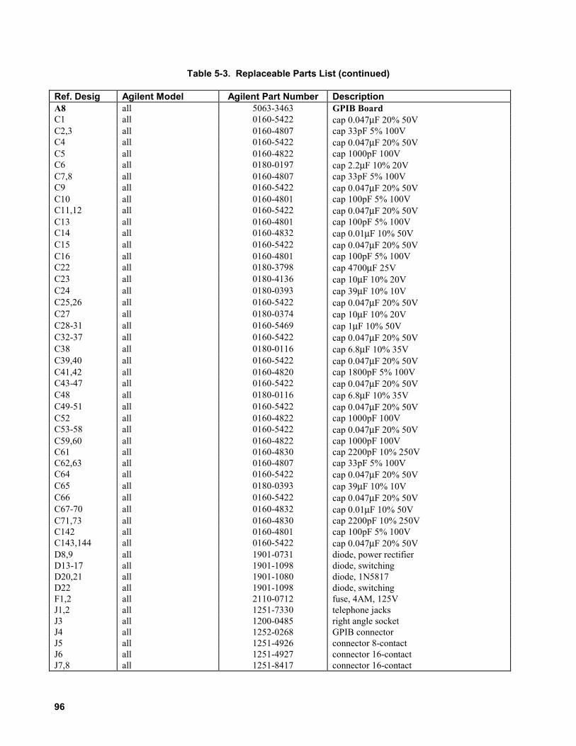
96
Table 5-3. Replaceable Parts List (continued)
Ref. Desig Agilent Model Agilent Part Number DescriptionA8 all 5063-3463 GPIB BoardC1 all 0160-5422 cap 0.047µF 20% 50VC2,3 all 0160-4807 cap 33pF 5% 100VC4 all 0160-5422 cap 0.047µF 20% 50VC5 all 0160-4822 cap 1000pF 100VC6 all 0180-0197 cap 2.2µF 10% 20VC7,8 all 0160-4807 cap 33pF 5% 100VC9 all 0160-5422 cap 0.047µF 20% 50VC10 all 0160-4801 cap 100pF 5% 100VC11,12 all 0160-5422 cap 0.047µF 20% 50VC13 all 0160-4801 cap 100pF 5% 100VC14 all 0160-4832 cap 0.01µF 10% 50VC15 all 0160-5422 cap 0.047µF 20% 50VC16 all 0160-4801 cap 100pF 5% 100VC22 all 0180-3798 cap 4700µF 25VC23 all 0180-4136 cap 10µF 10% 20VC24 all 0180-0393 cap 39µF 10% 10VC25,26 all 0160-5422 cap 0.047µF 20% 50VC27 all 0180-0374 cap 10µF 10% 20VC28-31 all 0160-5469 cap 1µF 10% 50VC32-37 all 0160-5422 cap 0.047µF 20% 50VC38 all 0180-0116 cap 6.8µF 10% 35VC39,40 all 0160-5422 cap 0.047µF 20% 50VC41,42 all 0160-4820 cap 1800pF 5% 100VC43-47 all 0160-5422 cap 0.047µF 20% 50VC48 all 0180-0116 cap 6.8µF 10% 35VC49-51 all 0160-5422 cap 0.047µF 20% 50VC52 all 0160-4822 cap 1000pF 100VC53-58 all 0160-5422 cap 0.047µF 20% 50VC59,60 all 0160-4822 cap 1000pF 100VC61 all 0160-4830 cap 2200pF 10% 250VC62,63 all 0160-4807 cap 33pF 5% 100VC64 all 0160-5422 cap 0.047µF 20% 50VC65 all 0180-0393 cap 39µF 10% 10VC66 all 0160-5422 cap 0.047µF 20% 50VC67-70 all 0160-4832 cap 0.01µF 10% 50VC71,73 all 0160-4830 cap 2200pF 10% 250VC142 all 0160-4801 cap 100pF 5% 100VC143,144 all 0160-5422 cap 0.047µF 20% 50VD8,9 all 1901-0731 diode, power rectifierD13-17 all 1901-1098 diode, switchingD20,21 all 1901-1080 diode, 1N5817D22 all 1901-1098 diode, switchingF1,2 all 2110-0712 fuse, 4AM, 125VJ1,2 all 1251-7330 telephone jacksJ3 all 1200-0485 right angle socketJ4 all 1252-0268 GPIB connectorJ5 all 1251-4926 connector 8-contactJ6 all 1251-4927 connector 16-contactJ7,8 all 1251-8417 connector 16-contact

97
Table 5-3. Replaceable Parts List (continued)
Ref. Desig Agilent Model Agilent Part Number DescriptionJ9 all 1251-4927 connector 16-contactJ10 all 1251-5384 connector 3-contactL1 all 9170-1680 chokeL2-4 all 9170-1454 core-shield beadQ1,4 all 1853-0089 transistor 2N4917R1 all 0757-0457 res 47.5 1% 1/8WR2 all 0698-3155 res 4.64K 1% 1/8WR3 all 0757-0442 res 10K 1% 1/8WR4 all 0698-3155 res 4.64K 1% 1/8WR5 all 0683-1065 res 10M 5% 1/4WR6 all 0698-4037 res 46.4 1% 1/8WR7 all 0698-3155 res 4.64K 1% 1/8WR8-11 all 0757-0401 res 100 1% 1/8WR12 all 0698-3155 res 4.64K 1% 1/8WR14 all 0698-0082 res 464 1% 1/8WR15-17 all 0698-4037 res 46.4 1% 1/8WR18 all 0757-0280 res 1K 1% 1/8WR19 all 0698-8827 res 1M 1% 1/8WR20-22 all 0698-3155 res 4.64K 1% 1/8WR23 all 0698-0082 res 464 1% 1/8WR24,26 all 0698-3156 res 14.7K 1% 1/8WR28 all 0699-0059 res 5K 0.1% 1/10WR29 all 2100-3353 trimmer 20K 10%R30 all 0699-0642 res 10K 0.1% 1/10WR32 all 0757-0457 res 47.5K 1% 1/8WR33 all 0698-6360 res 10K 0.1% 1/8WR34 all 0757-0401 res 100 1% 1/8WR35 all 0699-0059 res 5K 0.1% 1/10WR36 all 0757-0316 res 42.2 1% 1/8WR37 all 0699-0642 res 10K 0.1% 1/10WR39 all 0757-0270 res 249K 1% 1/8WR40 all 2100-3353 trimmer 20K 10%R41 all 0757-0401 res 100 1% 1/8WR42 all 0757-0411 res 332 1% 1/8WR43 all 0699-0059 res 5K 0.1% 1/10WR44 all 0757-0316 res 42.2 1% 1/8WR45 all 0699-0642 res 10K 0.1% 1/10WR46 all 0757-0411 res 332 1% 1/8WR48 all 0757-0457 res 47.5K 1% 1/8WR49 all 0698-6360 res 10K 0.1% 1/8WR50 all 0757-0401 res 100 1% 1/8WR51 all 2100-3353 trimmer 20K 10%R52 all 0698-3156 res 14.7K 1% 1/8WR55,58 all 2100-3732 trimmer 500 10%R59,60 all 0698-3558 res 4.02K 1% 1/8WR61 all 2100-3732 trimmer 500 10%R62-64 all 0698-3558 res 4.02K 1% 1/8WR65 all 0757-0280 res 1K 1% 1/8WR66 all 0698-3558 res 4.02K 1% 1/8WR67 all 0698-6320 res 5K 0.1% 1/8W

98
Table 5-3. Replaceable Parts List (continued)
Ref. Desig Agilent Model Agilent Part Number DescriptionR68 all 0757-0400 res 90.9 1% 1/8WR69 all 0698-6320 res 5K 0.1% 1/8WR70 all 0757-0400 res 90.9 1% 1/8WR71 all 0698-6320 res 5K 0.1% 1/8WR72 all 0757-0400 res 90.9 1% 1/8WR73 all 0757-0451 res 24.3K 1% 1/8WR74 all 0757-0199 res 21.5K 1% 1/8WR75 all 2100-3273 trimmer 2K 10%R76 all 0698-3455 res 261K 1% 1/8WR78 all 0698-3156 res 14.7K 1% 1/8WR79,80 all 8159-0005 res 0 ohmR82 all 0698-0082 res 464 1% 1/8WR83-88 all 0698-3155 res 4.64K 1% 1/8WR89 all 0757-0280 res 1K 1% 1/8WR90,98,99 all 0698-3155 res 4.64K 1% 1/8WR101 all 0698-6360 res 10K 0.1% 1/8WR102 all 0698-3558 res 4.02K 1% 1/8WR103 all 0698-3455 res 261K 1% 1/8WR106 all 1810-0206 network, sip 10K X7R109,110 all 0698-3155 res 4.64K 1% 1/8WR111 all 0757-0316 res 42.2 1% 1/8WR112 all 1810-0305 network, sip 4.7K X8S1 all 3101-1973 GPIB switchTBl all 0360-2312 terminal block 4-contactU1 all 1826-0468 IC MC3423P1 0V-level detectU2 all 5080-2157 IC GAL programmedU4 all 1820-8773 IC 80C51 microprocessorU5 all 1826-1369 IC LT1021 voltage regulator 10VU6 all 5080-2624 IC EPROM AM27512U7 all 1826-2187 IC converter PM-7545U8 all 1818-4134 IC RAM MCM6164C55U9 all 1826-2187 IC converter PM-7545U11 all 1826-2187 IC converter PM-7545U12 all 1820-3210 IC UART MC68B50PU13 all 1990-0543 IC opto-isolatorU14 all 1821-1479 IC 80C196 microprocessorU16 all 1820-2724 IC latch 74HC373U19 all 1826-0161 IC LM324N quad op ampU20 all 1826-0609 IC 8-input multiplexerU24 all 1826-1475 IC LT1011 comparatorU25 all 1826-1896 IC LT1001 op ampU28 all 1990-1387 IC opto-isolatorU31 all 1820-6789 IC 75176B RS485 driverU32 all 1990-1387 IC opto-isolatorU33 all 1826-0536 IC LM340AK-5 voltage regulator 5VU35 all 5080-2156 IC GAL programmedU36 all 5080-2625 IC GAL programmedU37 all 1820-4185 IC DS3658N interfaceU64-69 all 1826-1896 IC LT1001 op ampU70 all 1818-4932 IC EEPROM NMC9346
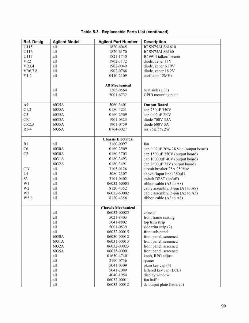
99
Table 5-3. Replaceable Parts List (continued)
Ref. Desig Agilent Model Agilent Part Number DescriptionU115 all 1820-6045 IC SN75ALS61610U116 all 1820-6170 IC SN75ALS6160U117 all 1821-1740 IC 9914 talker/listenerVR2 all 1902-3172 diode, zener 11VVR3,4 all 1902-0049 diode, zener 6.19VVR6,7,8 all 1902-0766 diode, zener 18.2VY1,2 all 0410-2109 oscillator 12MHz
A8 Mechanicalall 1205-0564 heat sink (U33)all 5001-6732 GPIB mounting plate
A9 6035A 5060-3401 Output BoardC1,2 6035A 0180-4231 cap 750µF 350VC3 6035A 0160-2569 cap 0.02µF 2KVCR1 6035A 1901-0325 diode 700V 35ACR2,3 6035A 1901-0759 diode 600V 3AR1-4 6035A 0764-0027 res 75K 5% 2W
Chassis ElectricalB1 all 3160-0097 fanC6 6030A 0160-2569 cap 0.02µF 20% 2KVdc (output board)C2 6030A 0180-3703 cap 1500µF 250V (output board)
6031A 0180-3493 cap 10000µF 40V (output board)6032A 0180-3491 cap 2600µF 75V (output board)
CB1 all 3105-0126 circuit breaker 25A 250VacL4 all 5080-2307 choke (input line) 380µHS3 all 3101-0402 switch DPST (on/off)W1 all 06032-60003 ribbon cable (A3 to A8)W2 all 8120-4352 cable assembly, 3-pin (A1 to A8)W3 all 06032-60002 cable assembly, 5-pin (A2 to A3)W5,6 all 8120-4356 ribbon cable (A2 to A8)
Chassis Mechanicalall 06032-00025 chassisall 5021-8403 front frame castingall 5041-8802 top trim stripall 5001-0539 side trim strip (2)all 06032-00015 front sub-panel6030A 06030-00012 front panel, screened6031A 06031-00013 front panel, screened6032A 06032-00023 front panel, screened6035A 06035-00001 front panel, screenedall 01650-47401 knob, RPG adjustall 2190-0736 spacerall 5041-0309 plain key cap (4)all 5041-2089 lettered key cap (LCL)all 4040-1954 display windowall 06032-00011 fan baffleall 06032-00012 dc output plate (lettered)

100
Table 5-3. Replaceable Parts List (continued)
Ref. Desig Agilent Model Agilent Part Number DescriptionChassis Mechanical
(cont)all 06032-00010 output buss bar (2)all 0340-1095 insulator for bus bar (4)all 0380-1362 standoff, 12mrn (buss bar) (2)all 1510-0044 binding post, rear panel groundall 0400-0086 insulated bushing (under A6) (2)all 5001-6739 cover, topall 5001-6738 cover, bottomall 06032-00024 cover, internal (lettered)all 5040-1626 cover, dc outputall 5040-1627 cover, ac inputall 5040-1625 strain relief (line cord)all 5062-3703 strap handle (2)all 5041-8819 handle retainer, front (2)all 5041-8820 handle retainer, back (2)all 5041-8801 foot (4)

101
6Component Location and Circuit DiagramsThis chapter contains component location diagrams, schematics, and other drawings useful for maintenance of the powersupply. Included in this section are:
a. Component location illustrations (Figures 6-1 through 6-9), showing the physical location and reference designators ofalmost all electrical parts. (Components located on the rear panel are easily identified.)
b. Notes (Table 6-1) that apply to all schematic diagrams.c. Schematic diagrams (Figures 6-10 through 6-13).
AC line voltage is present on the A1 Main Board Assembly whenever the power cord is connected to an ac power source.
Table 6-1. Schematic Diagram Notes
1. . denotes front-panel marking.
2. denotes rear-panel marking.
3. Complete reference designator consists of component reference designator prefixed with assembly number (e.g.:A2R14).
4. Resistor values are in ohms. Unless otherwise noted, resistors are either 1/4W, 5% or 1/8W, 1%. Parts list providespower rating and tolerance for all resistors.
5. Unless otherwise noted, capacitor values are in microfarads.
6. Square p.c. pads indicate one of the following:a. pin 1 of an integrated circuit.b. the cathode of a diode or emitter of a transistor.c. the positive end of a polarized capacitor.
7. Schematic components marked with an asterisk (*) indicate that different values are used in each model. Refer to theparts list for the applicable values.
8. Schematic components marked with a dagger († ) are listed under chassis, electrical in the parts list.
9. This capacitor is only used on 6030A and 6035A units. C6 is mounted on the chassis on 6030A units. C3 is mountedon the A9 board on 6035A units.
10. indicates multiple paths represented by only one line. Reference designators with pinnumbers indicate destination, or signal names identify individual paths. Numbersindicate number of paths represented by the line.
11. Inter-board commons have letter identifications (e.g.: ); commons existing on a single assembly have numberidentifications (e.g.: ).

102
Table 6-1. Schematic Diagram Notes (continued)
For single in-line resistor packages, pin 1 is marked with a dot. For integrated circuit packages, pin 1 is either marked witha dot, or pin 1 is to the left (as viewed from top) of indentation on the integrated circuit package (except for A8U6 andA8U8).
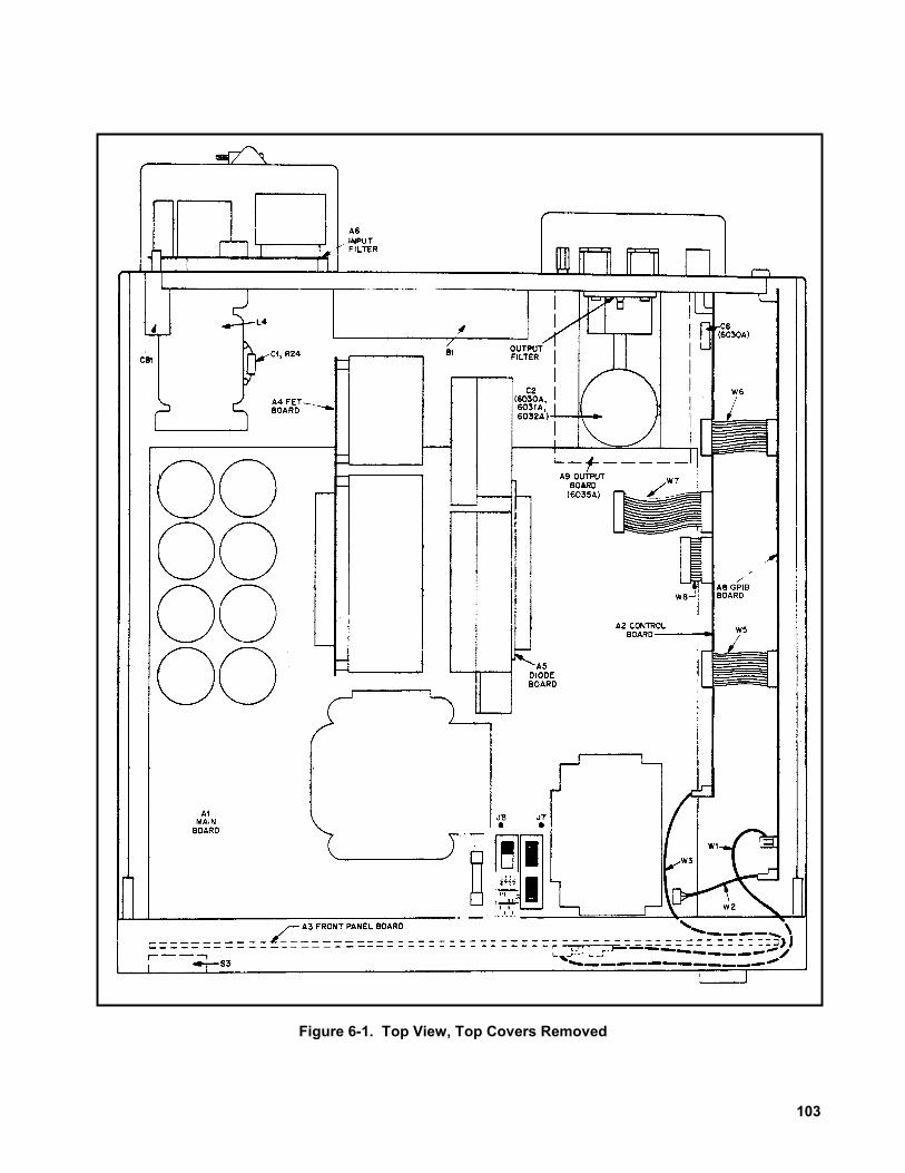
103
Figure 6-1. Top View, Top Covers Removed

104
Figure 6-2A. 6030A/35A Main Board (A1) and Output Filter Component Location
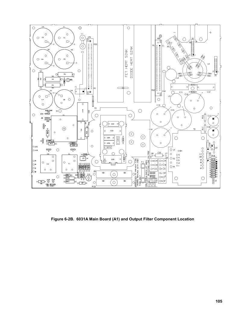
105
Figure 6-2B. 6031A Main Board (A1) and Output Filter Component Location
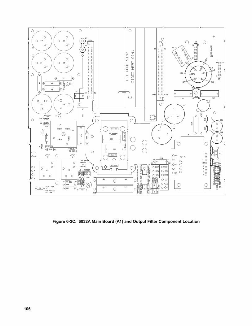
106
Figure 6-2C. 6032A Main Board (A1) and Output Filter Component Location

107
Figure 6-3. Control Board (A2) Component Location Figure 6-4. Front Panel Board (A3)Component Location
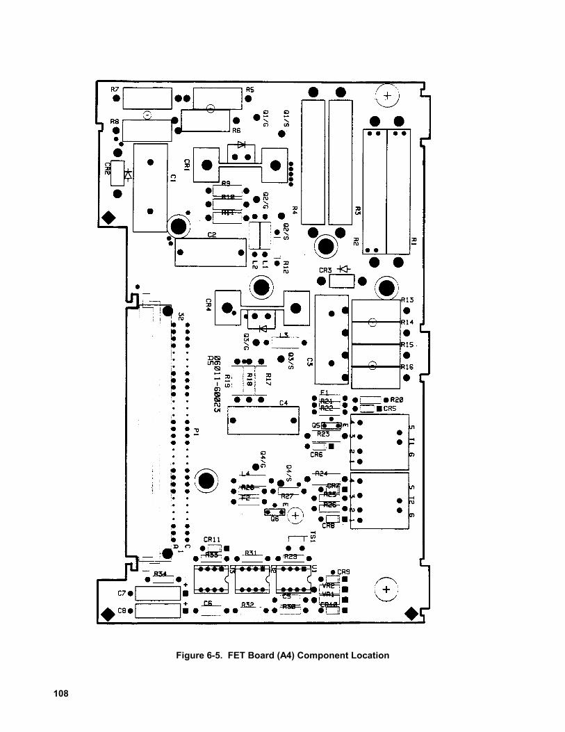
108
Figure 6-5. FET Board (A4) Component Location

109
Figure 6-6A. 6030A/35A Diode Board (A5) Component Location
Figure 6-6B. 6031A Diode Board (A5) Component Location

110
Figure 6-6C. 6032A Diode Board (A5) Component Location
Figure 6-7. AC Input Filter (A6) Component Location
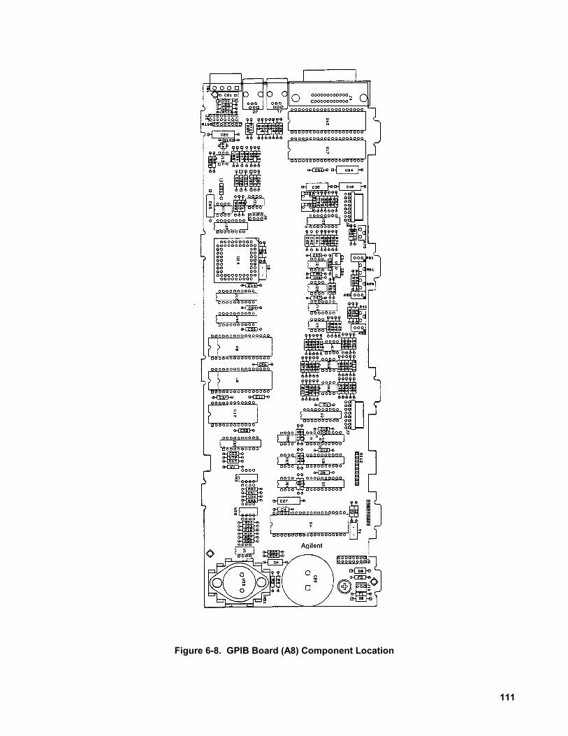
111
Figure 6-8. GPIB Board (A8) Component Location

112
Figure 6-9. 6035A Output Board (A9) Component Location
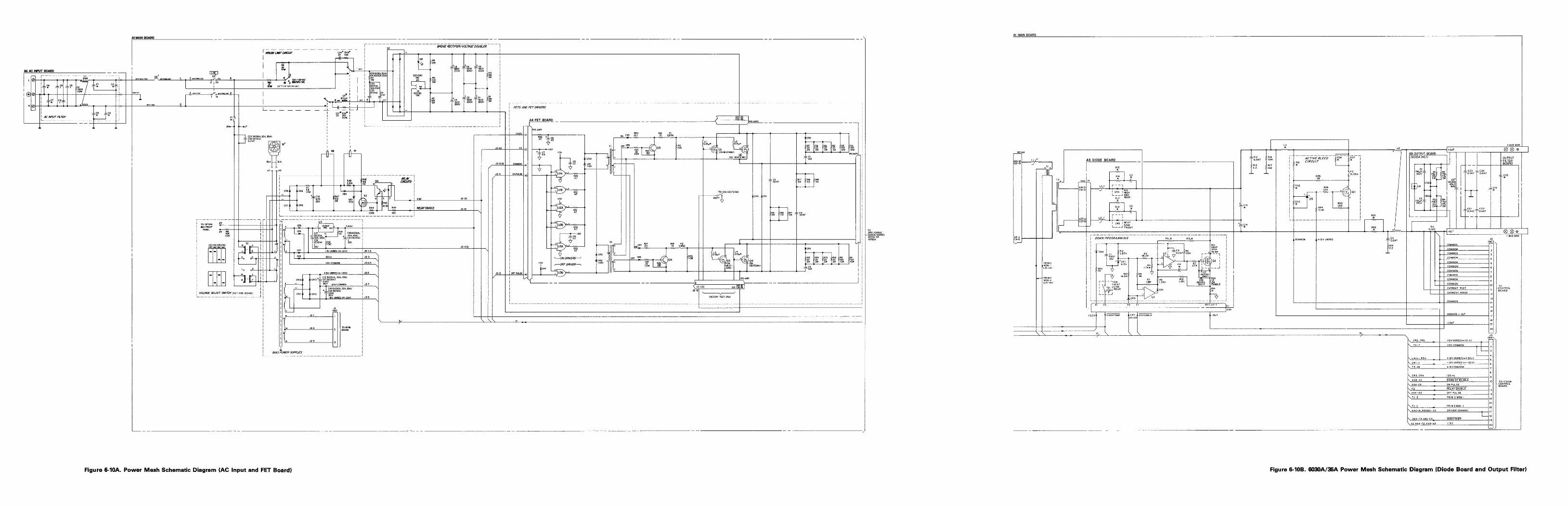
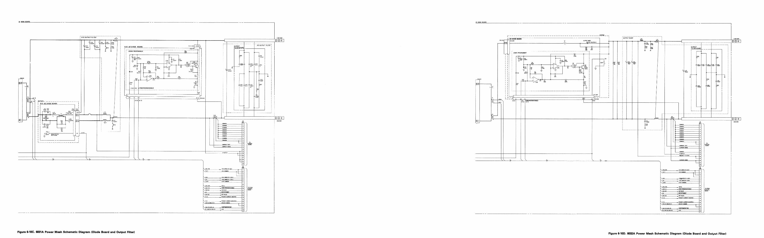


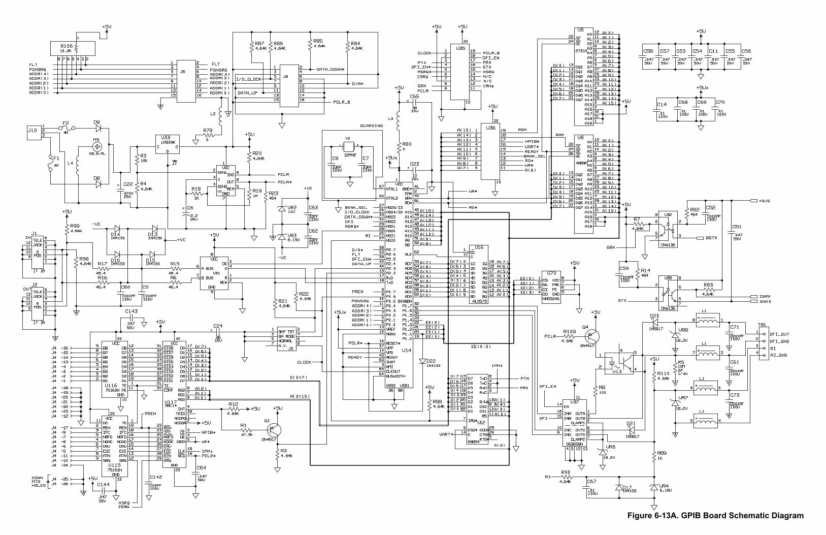
Figure 6-13A. GPIB Board Schematic Diagram

Figure 6-13B. GPIB Board Schematic Diagram

119
A
l00 Vac Input Power Option 100
General Information
Description
Option 100 is a modification of Agilent 6030A/31A/32A/35A power supplies that involves changing resistors on the A2board, recalibrating the supply, and changing the Front Panel. These changes allow the units to operate at a lower linevoltage of 87 to 106 Vac, while operating on the same line frequency of 48 to 63 Hz. The reduced input voltage limits theoutput power to approximately 700 watts. Other specifications that change due to Option 100 include ProgrammingResponse Time, Overvoltage Protection and Remote Analog Programming.
Scope of Appendix A
This appendix contains all the information necessary to support Agilent 6033A/31A/32A/35A power supplies that areequipped with Option 100. The appendix describes only the changes pertaining to Option 100 and how they affect the otherportions of this manual. Unless otherwise specified in Appendix A, all other portions of the annual apply to both thestandard unit and the Option 100 unit.
Suggestions for Using Appendix A
The Option 100 changes are listed sequentially, starting with Chapter 1 in the main body of the manual and working backthrough Chapter 6. It is recommended that the user mark all the necessary changes directly into his manual. This will updatethe manual for Option 100 and eliminate the need for constant referrals back to Appendix A.
Chapter 1 Manual Changes
On Page 9, in Scope change the output power from 1000 to 700 watts.
Chapter 2 Manual Changes
On Page 17, in Constant Voltage Full Scale Calibration step b, and Voltage Monitor and Remote Readback Full ScaleCalibration step b, change the VSET values to:
VSET 170 (6030A)VSET 50 (6032A)VSET 425 (6035A)

120
On Page 17, in Voltage Monitor and Remote Readback Full Scale Calibration step d, change the A8R58 adjustment to:170.025 ±6mV (6032A)50.0075 ± 1.52mV (6032A)425.063 ± 6µV (6035A)
On Page 17, in Voltage Monitor and Remote Readback Full Scale Calibration step c, change 5.000625V to:4.250625V ± 100µV (6030A/35A)4.167187V ± 100µV (6032A)
On Page 17, in Voltage Monitor and Remote Readback Full Scale Calibration step f, change the A8R61 adjustment tobetween:
170.00 and 170.50Vdc (6030A)50.00 and 50.025Vdc (6032A)425.00 and 425.125Vdc (6035A)
On Page 20, in Power Limit Calibration step a, change 240 Vdc to 206 Vdc.
On Page 20, in Power Limit Calibration step b, change the load resistor as follows:2.9 ohm 1500 W (6030A)0.05 ohm 1500 W (6031A)0.29 ohm 1500 W (6032A)32 ohm 1500 W (6035A)
On Page 20, in Power Limit Calibration step e, change the VSET values to:VSET 50 (6030A)VSET 6 (6031A)VSET 14.5 (6032A)VSET 163 (6035A)
On Page 20, in Power Limit Calibration step f, change the output values to:50 ± 1V (6030A)6 ± 0.08V (6031A)14.5 ± 0.1V (6032A)163 ± 1V (6035A)
On Page 20, in Power Limit Calibration step g, change the current and resistor settings to:32 ohm 1500W (6030A)0.50 ohm 1500W (6031A)2.8 ohm 1500W (6032A)212 ohm 1500W (6035A)
On Page 20, in Power Limit Calibration step i, change the VSET or ISET values to:VSET 170 (6030A)ISET 40 (6031A)VSET 50; ISET 18 (6032A)VSET 425 (6035A)
On Page 21, in Power Limit Calibration step j, change the output values to:170 ± 2V (6030A)@40A (6031A)50 ± 0.4V @17.5A (6032A)425 ± 0.4V @2A (6035A)
121
On Page 21, in Electronic load, make the following resistor changes:from 40 to 36 ohms (6030A)from 0.4 to 0.57 ohms (6031A)from 3.5 to 3 ohms (6032A)from 250 to 300 ohms (6035A)
from 3.5 to 2.4 ohms (6030A)from 0.069 to 0.043 ohms (6031A)from 0.4 to 0.27 ohms (6032A)from 40 to 30 ohms (6035A)
On Page 23, in Voltage Programming and Readback Accuracy step g, change the VSET values to:VSET 170 (6030A)VSET 50 (6032A)VSET 425 (6035A)
On Page 23, in Voltage Programming and Readback Accuracy step h, change the range values to:169.796 to 170.205Vdc (6030A)49.9375 to 50.0525Vdc (6032A)423.538 to 426.462Vdc (6035A)
On Page 23, in Voltage Programming and Readback Accuracy step i, change the values to:± 0.216Vdc (6030A)± 0.060Vdc (6032A)± 2.325Vdc (6035A)
On Page 23, in Load Effect (Load Regulation) step c, change the output voltage to:42Vdc (6030A)5.2Vdc (6031A)13.5Vdc (6032A)150Vdc (6035A)
On Page 24, in Load Effect (Load Regulation) step h, change the values to:0.009Vdc (6030A)0.0035Vdc (6031A)0.006Vdc (6032A)0.028Vdc (6035A)
On Page 24, in Source Effect (Line Regulation) step d, change the output voltage to:170Vdc (6030A)50Vdc (6032A)425Vdc (6035A)
On Page 25, in Source Effect (Line Regulation) step e, change the output current to:4.7Adc (6030A)35Adc (6032A)16Adc (6035A)1.38Adc (6035A)
On Page 25, in Source Effect (Line Regulation) step i, change the values to:0.022Vdc (6030A)0.008Vdc (6032A)0.055Vdc (6035A)

122
On Pages 25-27, in RMS Measurement Procedure, Peak Measurement and Load Transient Recovery Time, change theoutput voltage to
42Vdc (6030A)5.2Vdc (6031A)13.5Vdc (6032A)150Vdc (6035A)
On Page 28 and 29, in paragraph Current Programming and Readback Accuracy steps c and g, change the VSET values to:VSET 170 (6030A)VSET 50 (6032A)VSET 425 (6035A)
On Page 29, in Load Effect (Load Regulation) step c, change the output current to:4.7Adc (6030A)35Adc (6032A)16Adc (6035A)1.38Adc (6035A)
On Page 29, in Load Effect (Load Regulation) step cd change the output voltage to:170Vdc (6030A)50Vdc (6032A)425Vdc (6035A)
On Page 30, in Source Effect (Line Regulation) step d, change the output current to:17Adc (6030A)120Adc (6032A)50Adc (6035A)5Adc (6035A)
On Page 30, in Source Effect (Line Regulation) step e, change the output voltage to:42Vdc (6030A)5.2Vdc (6031A)13.5Vdc (6032A)150Vdc (6035A)
On Page 30, in PARD Ripple and Noise, make the following resistor changes:from 3.5 to 2.4 ohms (6030A)from 0.069 to 0.043 ohms (6031A)from 0.4 to 0.27 ohms (6032A)from 40 to 30 ohms (6035A)
On Page 30, Initialization, change step 2 as follows:2. Turn the power on, and depending on your unit's model number, send the following strings:
"EEINIT 6030" ''EEINIT 6031''"EEPROM 10,4,175.00" ''EEPROM 10,4,17.5"
''EEINIT 6032" "EEINIT 6035""EEPROM 10,4,51.495" "EEPROM 10,4,437.50"

123
Chapter 3 Manual Changes:
On Page 45, in Readback Multiplexer (U20), change Node U20-9, Measurement from + 5V to:+ 4.25V (6030A/31A/35A)+ 4.167V (6032A)
On Page 53 in Main Troubleshooting and on Page 54 in Troubleshooting No-Out Failures step d, change 320Vdc to250Vdc.
Chapter 4 Manual Changes:
On Page 74 In Power Mesh and Input Circuits, change 320Vdc to 250Vdc.
Chapter 5 and 6 Manual Changes
On Page 86, change the A2 board from:06030-60022 to 06030-60026 (6030A)06011-60022 to 06031-60026 (6031A)06032-60022 to 06032-60026 (6032A)06030-60028 to 06035-60020 (6035A)
On Page 91 and on the schematic diagram Figure 6-10, change R81 to:1.82K, 1% 1/8W Agilent P/N 0757-0429 (6030A, 6035A only)1.78K, 1% 1/8W Agilent P/N 0757-0278 (6032A only)
On Page 92 and on the schematic diagram Figure 6-10, change R92 to:10K, 1% 1/8W Agilent P/N 0757-0442 (6030A, 6035A only)34.8K, 1% 1/8W Agilent P/N 0757-0123 (6031A only)11.5K, 1% 1/8W Agilent P/N 0698-5383 (6032A only)
On Page 94, add option 100 label (A2 board) 9320-5540.
On Page 102, change front panel from:06030-00012 to 06030-00011 (6030A)06031-00013 to 06031-00012 (6031A)06032-00023 to 06032-00022 (6032A)06035-00001 to 06035-00003 (6035A)
On Page 103, add line voltage label (rear panel) Agilent P/N 06032-81004.


125
BBlank Front Panel Option 001
Introduction
This appendix describes the blank front panel option (Option 001) for the Agilent 6030A/31A/32A power supplies. Option001 is designed for applications in which front panel operation and monitoring are unnecessary. It has no front-panelcontrols and indicators except for the LINE switch and OVP ADJUST control found on the standard unit, and a pilot lightto indicate when ac input power is turned on. All other characteristics of the standard are retained.
Except for references to front-panel controls and indicators, most of the information in the manual applies to Option 001units. No attempt has been made in this appendix to change every reference to front-panel controls and indicators. Ingeneral, information in this appendix replaces only those procedures whose modification may not be obvious to the user.When reading the manual, the user can usually skip over references to front-panel controls and indicators other than theLINE switch and OVP ADJUST control.
Troubleshooting
The major difference between troubleshooting an Option 001 unit and a standard power supply is that the front panel is notavailable to help you isolate the problem to a specific section in the power supply. If you know which section of the supplyis defective, simply go to that section in the troubleshooting procedure and troubleshoot as described in Chapter 3.
To help you isolate the problem to a specific area of the supply, use the flowchart provided in this section.
If you cannot isolate the problem using the flowchart, you could replace the blank front panel of your supply with a standardfront panel and then troubleshoot the unit. Part numbers for front panel assemblies are provided in Chapter 5.
Chapter 2 Manual Changes:
On Page 20 Power Limit Calibration, change step f to read: Connect a DVM to control board test connector A2J7 pin 16(CC). Observe the DVM while adjusting A2R25 (POWER LIMIT) clockwise. Stop adjusting as soon as test point A2J7-16goes from high to low.
Note: You can also send an STS? query (or SCPI equivalent) in a looping program and monitor when the powersupply status changes to CC mode.
Under the Performance Tests section, any references to front panel control will have to be accomplished using GPIBcommands. Use the following guidelines:
1. To set the voltage and current to specific values, use the VSET and ISET (or SCPI equivalent) commands. 2. If the procedure says to check the CC or CV LED's, use an STS? query (or SCPI equivalent). A returned value of 1
indicates CV mode; a value of 2 indicates CC mode.

126
Chapter 3 Manual Changes:
Replace Figure 3-1 with the figure on the next page. SA Tables 3-5 through 3-7 do not apply to Option 001 units.
Chapter 5 and 6 Manual Changes:
On Page 94 under A3 Front Panel Board, the only part that applies to the Option 001 unit is R72, the OVP-adjustpotentiometer. Change R72 from 2100-1775 to 2100-4060.
On Page 102 under Chassis Electrical, add Neon Pilot Light, P/N 1450-0647. Also add OVP Cable (R72), P/N 06032-60004. Under Chassis Mechanical, change screened front panel to:
06030-00010 (6030A)06031-00011 (6031A)06032-00021 (6032A)
On Figure 6-9, add the neon pilot light in series with R8, 33K, across pins 4 and 5 of transformer T3.
On Figure 6-12, the only part that applies to the Option 001 unit is R72, the OVP-adjust potentiometer.

127
Figure 3-1. Troubleshooting Isolation (option 001)


129
CAgilent 6030A Test Record
Performance Test Record - Agilent 6030A POWER SUPPLY (Page 1 of 2)
Test Facility:
__________________________________________ Report No.____________________________________________________________________________________ Date_________________________________________________________________________________________ Customer_____________________________________________________________________________________ Tested By___________________________________________
Model Agilent 6030A Ambient Temperature _______________________________°CSerial No.__________________________________ Relative Humidity ___________________________________%Options ____________________________________ Nominal Line Frequency ____________________Hz (nominal)Firmware Revision ___________________________
Special Notes:____________________________________________________________________________________________________________________________________________________________________________________________________________________________________________________________________________________________________________________________________________________________________________________________________________________________________________________________________________________________________________________________________________________________________________________________________________________________________________________________________________________________________________________________________________________________________________________________________________________________________________________________
Test Equipment Used
Description Model No. Trace No. Cal. Due Date
1. AC Source _______________ _____________________________ _________________2. DC Voltmeter Agilent 3458A _____________________________ _________________3. RMS Voltmeter Agilent 3400A _____________________________ _________________4. Oscilloscope Agilent 54504A _____________________________ _________________5. Electronic Load Agilent 6050A and _____________________________ _________________
Agilent 60503A6. Current Probe _______________ _____________________________ _________________7. Current Shunt Guildline 9230/100 _____________________________ ________________________________ _______________ _____________________________ ________________________________ _______________ _____________________________ ________________________________ _______________ _____________________________ ________________________________ _______________ _____________________________ ________________________________ _______________ _____________________________ _________________

130
Performance Test Record - Agilent 6030A POWER SUPPLY (Page 2 of 2)
MODEL Agilent 6030A Report No.______________ Date_____________________
PageNo.
Test Description Minimum Spec. Results*
MaximumSpec.
MeasurementUncertainty
Constant Voltage Tests
23 Voltage Programming and ReadbackLow Voltage (0.500V) Front Panel Display GPIB Readback
0.354VOUT - 0.065VOUT - 0.080
________V________V________V
0.645VOUT + 0.065VOUT + 0.080
7µV7µV7µV
High Voltage (200V) Front Panel Display GPIB Readback
199.785VOUT - 0.72VOUT - 0.24
________V________V________V
200.215VOUT + 0.72VOUT + 0.24
2.7mV2.7mV2.7mV
23 Load Effect (60.0V) VOUT - 0.011 _______mV VOUT + 0.011 40µV
24 Source Effect (200V) VOUT - 0.011 _______mV VOUT + 0.011 350µV
2526
PARD (Ripple and Noise)RMSPeak-to-Peak
00
_______mV_______mV
0.0220.050
3.3mV1.5mV
27 Transient Recovery(90% to 100% Full Load)
0 _______mV 0.150/2ms 18mV
Constant Current Tests
28 Current Programming and Readback
Low Current (0.50A) Front Panel Display GPIB Readback
0.475IOUT - 0.017IOUT - 0.017
________A________A________A
0.525IOUT + 0.017IOUT + 0.017
220µA220µA220µA
High Current (17.0A) Front Panel Display GPIB Readback
16.941IOUT - 0.081IOUT - 0.076
________A________A________A
17.059IOUT + 0.081IOUT + 0.076
7mA7mA7mA
29 Load Effect (5.0A) IOUT - 0.010 ________mA IOUT + 0.010 2µA
29 Source Effect (17.0A) IOUT - 0.006 ________mA IOUT + 0.006 15µA
30 PARD (Ripple and Noise) 0 ________mA 0.015 2mA

131
DAgilent 6031A Test Record
Performance Test Record - Agilent 6031A POWER SUPPLY (Page 1 of 2)
Test Facility:
__________________________________________ Report No.____________________________________________________________________________________ Date_________________________________________________________________________________________ Customer_____________________________________________________________________________________ Tested By___________________________________________
Model Agilent 6031A Ambient Temperature _______________________________°CSerial No.__________________________________ Relative Humidity ___________________________________%Options ____________________________________ Nominal Line Frequency ____________________Hz (nominal)Firmware Revision ___________________________
Special Notes:________________________________________________________________________________________________________________________________________________________________________________________________________________________________________________________________________________________________________________________________________________________________________________________________________________________________________________________________________________________________________________________________________________________________________________________________________________________________________________________________________________________________________________________________________________________________
Test Equipment Used
Description Model No. Trace No. Cal. Due Date
1. AC Source _______________ _____________________________ _________________2. DC Voltmeter Agilent 3458A _____________________________ _________________3. RMS Voltmeter Agilent 3400A _____________________________ _________________4. Oscilloscope Agilent 54504A _____________________________ _________________5. Electronic Load Agilent 6050A and _____________________________ _________________
Agilent 60504A6. Current Probe _______________ _____________________________ _________________7. Current Shunt Guildline 9230/300 _____________________________ ________________________________ _______________ _____________________________ ________________________________ _______________ _____________________________ ________________________________ _______________ _____________________________ ________________________________ _______________ _____________________________ ________________________________ _______________ _____________________________ _________________
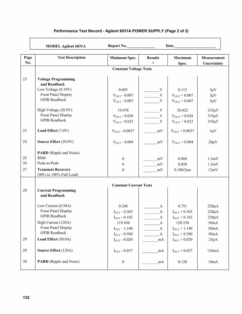
132
Performance Test Record - Agilent 6031A POWER SUPPLY (Page 2 of 2)
MODEL Agilent 6031A Report No.______________ Date_____________________
PageNo.
Test Description Minimum Spec. Results*
MaximumSpec.
MeasurementUncertainty
Constant Voltage Tests
23 Voltage Programming and ReadbackLow Voltage (0.10V) Front Panel Display GPIB Readback
0.085VOUT - 0.007VOUT - 0.007
________V________V________V
0.115VOUT + 0.007VOUT + 0.007
3µV3µV3µV
High Voltage (20.0V) Front Panel Display GPIB Readback
19.978VOUT - 0.028VOUT - 0.023
________V________V________V
20.022VOUT + 0.028VOUT + 0.023
335µV335µV335µV
23 Load Effect (7.0V) VOUT - 0.0037 _______mV VOUT + 0.0037 1µV
24 Source Effect (20.0V) VOUT - 0.004 _______mV VOUT + 0.004 20µV
2526
PARD (Ripple and Noise)RMSPeak-to-Peak
00
_______mV_______mV
0.0080.050
1.2mV1.5mV
27 Transient Recovery(90% to 100% Full Load)
0 _______mV 0.100/2ms 12mV
Constant Current Tests28 Current Programming
and Readback
Low Current (0.50A) Front Panel Display GPIB Readback
0.248IOUT - 0.303IOUT - 0.102
________A________A________A
0.751IOUT + 0.303IOUT + 0.102
220µA220µA220µA
High Current (120A) Front Panel Display GPIB Readback
119.450IOUT - 1.140IOUT - 0.580
________A________A________A
120.550IOUT + 1.140IOUT + 0.580
50mA50mA50mA
29 Load Effect (50.0A) IOUT - 0.020 ________mA IOUT + 0.020 25µA
29 Source Effect (120A) IOUT - 0.037 ________mA IOUT + 0.037 136mA
30 PARD (Ripple and Noise) 0 ________mA 0.120 18mA
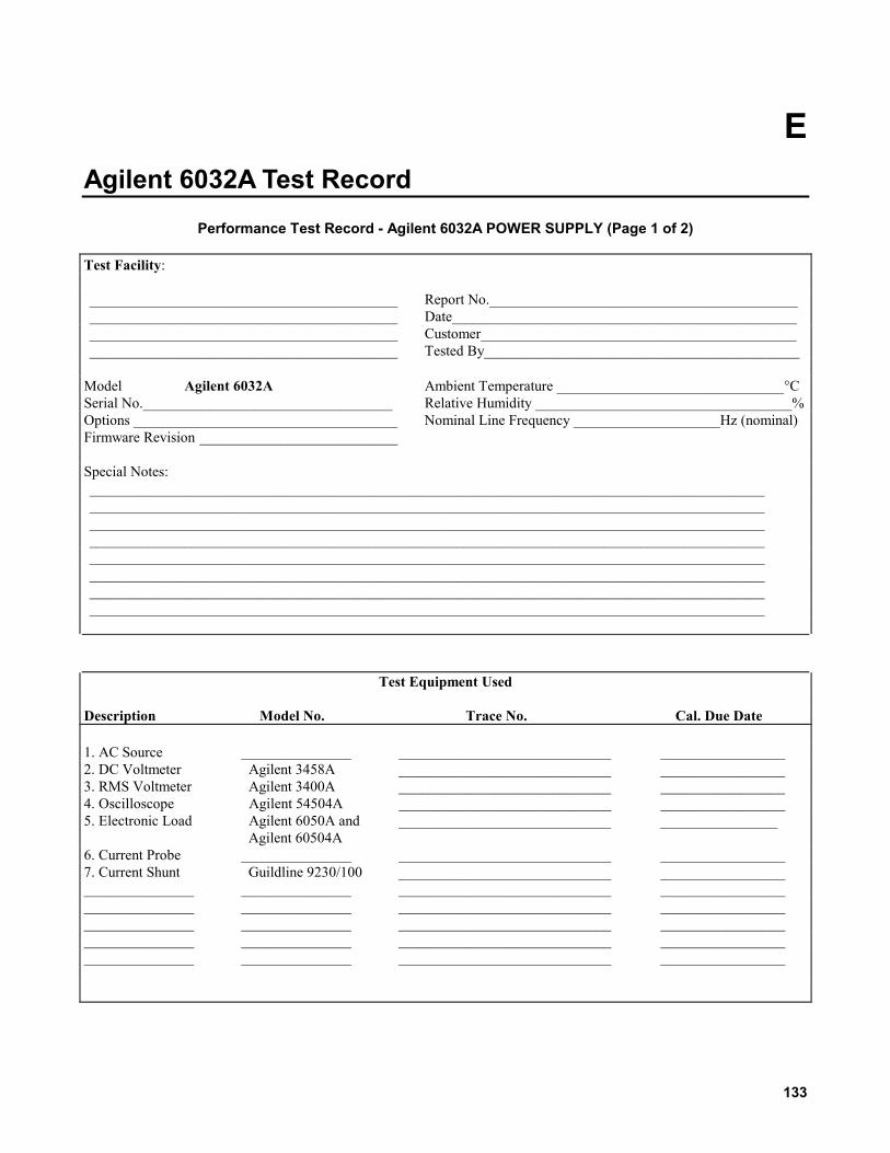
133
EAgilent 6032A Test Record
Performance Test Record - Agilent 6032A POWER SUPPLY (Page 1 of 2)
Test Facility:
__________________________________________ Report No.____________________________________________________________________________________ Date_________________________________________________________________________________________ Customer_____________________________________________________________________________________ Tested By___________________________________________
Model Agilent 6032A Ambient Temperature _______________________________°CSerial No.__________________________________ Relative Humidity ___________________________________%Options ____________________________________ Nominal Line Frequency ____________________Hz (nominal)Firmware Revision ___________________________
Special Notes:________________________________________________________________________________________________________________________________________________________________________________________________________________________________________________________________________________________________________________________________________________________________________________________________________________________________________________________________________________________________________________________________________________________________________________________________________________________________________________________________________________________________________________________________________________________________
Test Equipment Used
Description Model No. Trace No. Cal. Due Date
1. AC Source _______________ _____________________________ _________________2. DC Voltmeter Agilent 3458A _____________________________ _________________3. RMS Voltmeter Agilent 3400A _____________________________ _________________4. Oscilloscope Agilent 54504A _____________________________ _________________5. Electronic Load Agilent 6050A and _____________________________ ________________
Agilent 60504A6. Current Probe _______________ _____________________________ _________________7. Current Shunt Guildline 9230/100 _____________________________ ________________________________ _______________ _____________________________ ________________________________ _______________ _____________________________ ________________________________ _______________ _____________________________ ________________________________ _______________ _____________________________ ________________________________ _______________ _____________________________ _________________

134
Performance Test Record - Agilent 6032A POWER SUPPLY (Page 2 of 2)
MODEL Agilent 6032A Report No.______________ Date_____________________
PageNo.
Test Description Minimum Spec. Results*
MaximumSpec.
MeasurementUncertainty
Constant Voltage Tests23 Voltage Programming
and ReadbackLow Voltage (0.090V) Front Panel Display GPIB Readback
0.050VOUT - 0.020VOUT - 0.020
________V________V________V
0.130VOUT + 0.020VOUT + 0.020
3µV3µV3µV
High Voltage (60.0V) Front Panel Display GPIB Readback
59.939VOUT - 0.118VOUT - 0.068
________V________V________V
60.061VOUT + 0.118VOUT + 0.068
845µV845µV845µV
23 Load Effect (20.0V) VOUT - 0.007 _______mV VOUT + 0.007 20µV
24 Source Effect (60.0V) VOUT - 0.009 _______mV VOUT + 0.009 40µV
2526
PARD (Ripple and Noise)RMSPeak-to-Peak
00
_______mV_______mV
0.0060.040
900µV1.2mV
27 Transient Recovery(90% to 100% Full Load)
0 _______mV 0.100/2ms 12mV
Constant Current Tests
28 Current Programming and Readback
Low Current (0.50A) Front Panel Display GPIB Readback
0.414IOUT - 0.041IOUT - 0.036
________A________A________A
0.586IOUT + 0.041IOUT + 0.036
220µA220µA220µA
High Current (50.0A) Front Panel Display GPIB Readback
49.815IOUT - 0.270IOUT - 0.215
________A________A________A
50.185IOUT + 0.270IOUT + 0.215
20mA20mA20mA
29 Load Effect (16.5A) IOUT - 0.011 ________mA IOUT + 0.011 15µA
29 Source Effect (50.0A) IOUT - 0.015 ________mA IOUT + 0.015 25µA
30 PARD (Ripple and Noise) 0 ________mA 0.025 3.7A

135
FAgilent 6035A Test Record
Performance Test Record - Agilent 6035A POWER SUPPLY (Page 1 of 2)
Test Facility:
__________________________________________ Report No.____________________________________________________________________________________ Date_________________________________________________________________________________________ Customer_____________________________________________________________________________________ Tested By___________________________________________
Model Agilent 6035A Ambient Temperature _______________________________°CSerial No.__________________________________ Relative Humidity ___________________________________%Options ____________________________________ Nominal Line Frequency ____________________Hz (nominal)Firmware Revision ___________________________
Special Notes:________________________________________________________________________________________________________________________________________________________________________________________________________________________________________________________________________________________________________________________________________________________________________________________________________________________________________________________________________________________________________________________________________________________________________________________________________________________________________________________________________________________________________________________________________________________________
Test Equipment Used
Description Model No. Trace No. Cal. Due Date
1. AC Source _______________ _____________________________ _________________2. DC Voltmeter Agilent 3458A _____________________________ _________________3. RMS Voltmeter Agilent 3400A _____________________________ _________________4. Oscilloscope Agilent 54504A _____________________________ _________________5. Electronic Load Agilent 6050A and _____________________________ _________________
Agilent 60503A6. Current Probe _______________ _____________________________ _________________7. Current Shunt Guildline 9230/15 _____________________________ _________________8. Power Resistor 250 ohms 1% _____________________________ _________________
1KW (min.) _____________________________ ________________________________ _______________ _____________________________ ________________________________ _______________ _____________________________ ________________________________ _______________ _____________________________ _________________

136
Performance Test Record - Agilent 6035A POWER SUPPLY (Page 2 of 2)
MODEL Agilent 6035A Report No.______________ Date_____________________
PageNo.
Test Description Minimum Spec. Results*
MaximumSpec.
MeasurementUncertainty
Constant Voltage Tests
23 Voltage Programming and ReadbackLow Voltage (1.00V) Front Panel Display GPIB Readback
0.598VOUT - 0.300VOUT - 0.205
________V________V________V
1.400VOUT + 0.300VOUT + 0.205
12µV12µV12µV
High Voltage (500V) Front Panel Display GPIB Readback
498.350VOUT - 3.500VOUT - 2.700
________V________V________V
501.650VOUT + 3.500VOUT + 2.700
6.5mV6.5mV6.5mV
23 Load Effect (200V) VOUT - 0.060 _______mV VOUT + 0.060 350µV
24 Source Effect (500V) VOUT - 0.063 _______mV VOUT + 0.063 800µV
2526
PARD (Ripple and Noise)RMSPeak-to-Peak
00
_______mV_______mV
0.0500.160
7.5mV4.8mV
27 Transient Recovery(90% to 100% Full Load)
0 _______mV 0.200/5ms 24mV
Constant Current Tests
28 Current Programming and Readback
Low Current (0.10A) Front Panel Display GPIB Readback
0.015IOUT - 0.060IOUT - 0.050
________A________A________A
0.185IOUT + 0.060IOUT + 0.050
56µA56µA56µA
High Current (5.0A) Front Panel Display GPIB Readback
4.900IOUT - 0.085IOUT - 0.075
________A________A________A
5.100IOUT + 0.085IOUT + 0.075
2mA2mA2mA
29 Load Effect (2.0A) IOUT - 0.034 ________mA IOUT + 0.034 2µA
29 Source Effect (5.0A) IOUT - 0.018 ________mA IOUT + 0.018 2µA
30 PARD (Ripple and Noise) 0 ________mA 0.050 5mA

137
GManual BackdatingThis section describes changes that must be made to the manual so that it applies to instruments with serial numbers lowerthan those listed on the title page. Look in the following table for the serial number of your instrument, and make only thosechanges listed for your instrument. Note that for some changes you may be instructed to update the instrument if certaincomponents are being replaced during repair. __________________________________________| Prefix | Serial Number | Make Changes || 6030A || 2934A | 01825-01829 | 1-7, 9, 10, 12, 14-18 || 3023A | 01925-02408 | 1-7, 9, 10, 12, 14-18 || 3123A | 02409-02538 | 1-7, 9, 10, 12, 14-18 || 3137A | 02539-02568 | 1-7, 9, 10, 12, 14-17 || 3141A | 02569-02748 | 1-7, 9, 10, 12, 14-16 || 3211A | 02749-02778 | 1-7, 9, 10, 12, 14-16 || 3215A | 02779-02808 | 1-7, 9, 10, 12, 14, 15 || 3220A | 02809-03068 | 1-7, 9, 10, 12, 14 || 3251A | 03069-03108 | 1-7, 9, 10, 12 || 3305A | 03109-03308 | 1-7, 9, 10 || 3332A | 03309-03568 | 1-7, 9 || 3415A | 03569-03648 | 1-7 || 3430A | 03649-03708 | 1-6 || 3441A | 03709-03818 | 1-5 || 3506A | 03819-04088 | 1-4 || 3544A | 04089-04478 | 1-3 || 3702A | 04479-04848 | 1, 2 || US3702 | 0101-0260 | 1, 2 || US3832 | 0261-0300 | 1 || | | || | | || 6031A || 2934A | 01821-01825 | 1, 3-7, 9-12, 14, 16,17,18|| 3026A | 01921-02280 | 1, 3-7, 9-12, 14, 16,17,18|| 3121A | 02281-02410 | 1, 3-7, 9-12, 14, 16,17,18|| 3137A | 02411-02430 | 1, 3-7, 9-12, 14, 16, 17 || 3140A | 02431-02520 | 1, 3-7, 9-12, 14, 16 || 3213A | 02521-02560 | 1, 3-7, 9-12, 14, 16 || 3221A | 02561-02650 | 1, 3-7, 9-12, 14 || 3302A | 02651-02690 | 1, 3-7, 9-12 || 3304A | 02691-02700 | 1, 3-7, 9-11 || 3313A | 02701-02760 | 1, 3-7, 9-10 || 3325A | 02761-02920 | 1, 3-7, 9 || 3416A | 02921-02990 | 1, 3-7 || 3429A | 02991-03020 | 1, 3-6 || 3440A | 03021-03110 | 1, 3-5 || 3506A | 03111-03280 | 1, 3, 4 || 3543A | 03281-03890 | 1, 3 || US3543 | 0101-0340 | 1, 3 || US3831 | 0341-0375 | 1 |
__________________________________________| Prefix | Serial Number | Make Changes || 6032A || 3004A | 05881-05885 | 1, 3-7, 9-12, 14, 17, 18 || 3023A | 06181-07180 | 1, 3-7, 9-12, 14, 17, 18 || 3123A | 07181-07480 | 1, 3-7, 9-12, 14, 17, 18 || 3138A | 07481-07880 | 1, 3-7, 9-12, 14, 17 || 3211A | 07881-08020 | 1, 3-7, 9-12, 14, 17 || 3221A | 08021-08200 | 1, 3-7, 9-12, 14 || 3232A | 08201-08480 | 1, 3-7, 9-12, 14 || 3250A | 08481-08560 | 1, 3-7, 9-12 || 3304A | 08561-08780 | 1, 3-7, 9-11 || 3319A | 08781-08820 | 1, 3-7, 9, 10 || 3304A | 08821-08860 | 1, 3-7, 9, 10 || 3319A | 08861-08980 | 1, 3-7, 9, 10 || 3323A | 08981-09580 | 1, 3-7, 9 || 3415A | 09581-09900 | 1, 3-7 || 3431A | 09901-10140 | 1, 3-6 || 3440A | 10141-10580 | 1, 3-5 || 3510A | 10581-11160 | 1, 3-4 || 3542A | 11161-13020 | 1, 3 || US3542 | 0101-0880 | 1, 3 || US3832 | 0881-1025 | 1 || | | || 6035A || 3038A | 00101-00177 | 1-10, 12-18 || 3124A | 00178-00217 | 1-10, 12-18 || 3140A | 00218-00297 | 1-10, 12-16 || 3211A | 00298-00317 | 1-10, 12-15 || 3224A | 00318-00347 | 1-10, 12-14 || 3239A | 00348-00387 | 1-10, 12, 13 || 3251A | 00388-00417 | 1-10, 12 || 3308A | 00418-00477 | 1-10 || 3330A | 00478-00517 | 1-9 || 3330A | 00518-00537 | 1-9 || 3351A | 00538-00597 | 1-8 || 3418A | 00598-00637 | 1-7 || 3432A | 00638-00682 | 1-5 || 3512A | 00683-00862 | 1-4 || 3542A | 00863-01112 | 1-3 || 3702A | 01113-01342 | 1,2 || US3702 | 0101-0250 | 1,2 || US3832 | 0251-0280 | 1 |

138
CHANGE 1:Under A1 Main Board, change R45 to 82.5k p/n 0757-0563.
CHANGE 2:Under A8 GPIB Board.Add: R100 p/n 0698-4037. U17 p/n 1820-2549Delete: C67-70 0.01uF 10%, p/n 0160-4832, qty 4. C71,73 2200pF 10%, p/n 0160-4830, qty 2. L1 choke, p/n 9170-1680. L2-4 core-shield bead, p/n 9170-1454, qty 3. : Q1 transistor 2N4917, p/n 1853-0089. R1 47.5K 1%, p/n 0757-0457. R2,12 4.64K 1%, p/n 0698-3155, qty 2. R79,80 0 ohm, p/n 8159-0005, qty 2. U117 IC-9914 talker/listener, p/n 1821-1740.Change: A8, GPIB board to p/n 5060-3551. C14 to 0.047uF, p/n 0160-5422. C23 to 39uF, p/n 0180-0393. C61 to p/n 0160-4281. U6 to p/n 5080-2160. U36 to p/n 5080-2158.
CHANGE 3:Under A5 Diode Board, change CR4 and CR5 for model6030A to p/n 1901-1182. Change CR4 and CR5 formodel 6035A to p/n 1901-1316. Change Q1 for model6030A to p/n 1855-0486 and for model 6035A to p/n1855-0802. Under A5 Mechanical, change heatsink(CR5) for models 6030A,35A to p/n 06030-00003.Change heatsink (CR4, Q1) for models 6030A,35A top/n 06030-00004.
CHANGE 4:Under A4 FET Board, change CR1 and CR4 to p/n1901-1137. Both diodes must be the same part number.
CHANGE 5:Under A8 GPIB Board, change U33 to p/n 1820-0430.
CHANGE 6:Under A8 GPIB Board, change U14 to p/n 1820-6721.
CHANGE 7:Under A8 GPIB Board:Add: U15, p/n 1LH4-0001.Delete: U115, SN75ALS61610, p/n 1820-6045. U116, SN75ALS6160, p/n 1820-6170. C142 100pF, p/n 0160-4801. C143-144 .047uF, p/n 0160-5422.Change: A8, GPIB board to p/n 5060-3305.
CHANGE 8:Under A1 Main Board, change K1, K2 to p/n 0490-1746.Change R47 and R48 150 ohms p/n 0761-0035.
CHANGE 9:Under A2 Control Board,*********** For Model 6035A only ***********Change R40 to 95k p/n 0699-1211 and 1.21M p/n 0699-1271. Change R41 to 200k p/n 0698-6376.
CHANGE 10:Under A3 Front Panel, change G1 to p/n 06032-60005.On page 5-18 under Chassis Mechanical, change Knob top/n 0370-1303. Delete Spacer, p/n 2190-0736.
CHANGE 11:Under A1 Main Board,Add: C3, C7, 1400uF p/n 0180-3460 R6, 1.3k, p/n 0811-1803 U2, U4, rectifier, p/n 1906-0006Delete: C27, 34, cap 0.01uF 400V, p/n 0160-6805 CR6-13, power rectifier 400V, p/n 1901-0731 R24, res 200 5% 1/2W, p/n 0686-2015 R43, 44, res 2.61k 1% 1/8W, p/n 0698-0085 R45, res 82.5k 1% 1/8W, p/n 0757-0463 R46, res 681 1% 1/8W, p/n 0757-0419 R47, 48, res 150 5% 1W p/n 0761-0035 R49, res 100 1% 1/8W, p/n 0757-0401 Q2, FET N-channel, p/n 1855-0665 VR1, diode zener 7.5V 5%, p/n 1902-0955 U6, opto-isolator, p/n 1990-1074Change: A1 (6030A) to p/n 06030-60021 A1 (6031A) to p/n 06011-60021 A1 (6032A) to p/n 06032-60021 A1 (6035A) to p/n 06030-60027C1,2,4-6,8 to 1400uF p/n 0180-3460 C10 to 22uF p/n 0180-3696 CR1 to 1901-0028 DS1 to display, p/n 1990-0325 K1 to relay p/n 0490-1457 K2 to relay p/n 0490-1341. R5 to 300, p/n 0686-3015 R7 to 10, p/n 0686-1005 R8 to 33k, p/n 0686-3335 R41 to 30, p/n 0811-1869
Under A6 AC Input Filter, change the part number of theboard to 06011-60025 for models 6030A,31A,32A, and06011-60028 for model 6035A.
Under Chassis Electrical at the end of the parts list,change L4 to p/n 06011-80093.

139
CHANGE 12:Under A1 Main Board,*********** For Model 6031A only ***********Change C23 and C28 to .047uF Agilent p/n 0160-5895.Add C21 and C24, .047uF Agilent p/n 0160-5895.Add R21 and R22, 1 ohm p/n 0699-0208.*********** For Model 6032A only ***********Change C20 and C22 to .047uF Agilent p/n 0160-5895.Add C21 and C23, .047uF Agilent p/n 0160-5895.Add R20 and R23, 1 ohm p/n 0699-0208.
CHANGE 13:Under A8 GPIB Board, change U8 to p/n 1818-4111.
CHANGE 14:Under A1 Main Board, change C11,12 to 0.047uF, p/n0160-5895. On page 5-3, change R12 and R13 to 2.2ohms, p/n 0699-0188.
CHANGE 15:Under A8 GPIB Board, delete D22.
CHANGE 16:Under A5 Diode Board, delete L3.
CHANGE 17:Under A1 Main Board, change U1 to p/n 1906-0218.
CHANGE 18:Under A6 AC Input Filter, change L1 to p/n 06011-80094.

Manual Updates
The following updates have been made to this manual since the print revision indicated on the title page.
4/07/04
Pages 38, 104, 105, 106 and 107 have been corrected.