5 v stereo dac with 2 vrms ground-centered output · 2010-07-09 · notes: 3. measured at the...
TRANSCRIPT

CS4354
5 V Stereo DAC with 2 VRMS Ground-centered Output
FeaturesAdvanced Multi-bit Delta-Sigma Modulator
101 dB A-wt Dynamic Range
-86 dB THD+N
Single-ended Ground Centered Analog Architecture– No DC-blocking Capacitors Required– Integrated Inverting Charge Pump– Filtered Line-level Outputs– 2 VRMS Full-scale Output
Low-latency Digital Filtering
Supports Sample Rates up to 192 kHz
24-bit I²S Input
+5 V Analog Supply with Integrated Inverting Charge Pump and Regulator for Core Logic, and +1.8 V to +5 V Interface Power Supplies
50 mW Power Consumption
14-pin SOIC, Lead-free Assembly
Description
The CS4354 is a complete stereo digital-to-analog sys-tem including digital interpolation, third-order multi-bitdelta-sigma digital-to-analog conversion, digital de-em-phasis, analog filtering, and on-chip 2 VRMS line-leveldriver from a 5 V supply.
The advantages of this architecture include ideal differ-ential linearity, no distortion mechanisms due to resistormatching errors, no linearity drift over time and temper-ature, high tolerance to clock jitter, and a minimal set ofexternal components.
The CS4354 is available in a 14-pin SOIC package inCommercial (-40°C to +85°C) grade. The CDB4354Customer Demonstration Board is also available for de-vice evaluation and implementation suggestions.Please see “Ordering Information” on page 23 for com-plete details.
These features are ideal for cost-sensitive, 2-channelaudio systems including video game consoles, Blu-RayDisc® and DVD players, set-top boxes, digital TVs, andDAB/DMB devices.
PCM Serial Audio Port
Leve
l Sh
ifter
I²S SerialAudio Input
MultibitModulator
Interpolation Filters + HPF
Left Channel
Right Channel
Power-On Reset
Auto Speed Mode Detect
Analog Supply (VA)+5 V
Inverting Charge Pump
1.8V reg
-VA
Interface Supply (VL)+1.8V to +5V
Ground-Centered,2 Vrms Line Level Outputs
DAC
Copyright Cirrus Logic, Inc. 2010(All Rights Reserved)http://www.cirrus.com
Advance Product Information This document contains information for a new product. Cirrus Logic reserves the right to modify this product without notice.
JULY '10DS895A2

CS4354
TABLE OF CONTENTS1. PIN DESCRIPTIONS ........................................................................................................................... 42. CHARACTERISTICS AND SPECIFICATIONS ...................................................................................... 5
RECOMMENDED OPERATING CONDITIONS .................................................................................... 5ABSOLUTE MAXIMUM RATINGS ........................................................................................................ 5DAC ANALOG CHARACTERISTICS .................................................................................................... 6COMBINED DIGITAL AND ON-CHIP ANALOG FILTER CHARACTERISTICS ................................... 7SWITCHING SPECIFICATIONS - SERIAL AUDIO INTERFACE ......................................................... 8DIGITAL INTERFACE CHARACTERISTICS ....................................................................................... 10INTERNAL POWER-ON RESET THRESHOLD VOLTAGES ............................................................. 10DC ELECTRICAL CHARACTERISTICS .............................................................................................. 112.1 Digital I/O Pin Characteristics ........................................................................................................ 11
3. TYPICAL CONNECTION DIAGRAM ................................................................................................... 124. APPLICATIONS ................................................................................................................................... 13
4.1 Ground-Centered Line Outputs ...................................................................................................... 134.2 Sample Rate Range/Operational Mode Detect .............................................................................. 134.3 System Clocking ............................................................................................................................ 134.4 Serial Clock .................................................................................................................................... 14
4.4.1 External Serial Clock Mode ................................................................................................... 144.4.2 Internal Serial Clock Mode .................................................................................................... 14
4.4.2.1 De-Emphasis Control ................................................................................................. 144.5 Internal High-Pass Filter ................................................................................................................ 154.6 Digital Interface Format .................................................................................................................. 154.7 Internal Power-On Reset ............................................................................................................... 154.8 Initialization .................................................................................................................................... 164.9 Recommended Power-Up and Power-Down Sequences .............................................................. 18
4.9.1 Power-Up Sequence ............................................................................................................. 184.9.2 Power-Down Sequence ......................................................................................................... 18
4.10 Grounding and Power Supply Arrangements .............................................................................. 184.10.1 Capacitor Placement ........................................................................................................... 18
5. COMBINED DIGITAL AND ON-CHIP ANALOG FILTER RESPONSE PLOTS .............................. 196. PARAMETER DEFINITIONS ................................................................................................................ 217. PACKAGE INFORMATION .................................................................................................................. 22
7.1 Dimensions .................................................................................................................................... 227.2 Thermal Characteristics ................................................................................................................. 22
8. ORDERING INFORMATION ................................................................................................................ 239. REVISION HISTORY ............................................................................................................................ 24
LIST OF FIGURESFigure 1. External Serial Clock Mode Input Timing ..................................................................................... 9Figure 2. Internal Serial Clock Mode Input Timing ...................................................................................... 9Figure 3. Internal Serial Clock Generation .................................................................................................. 9Figure 4. Power-On Reset Threshold Sequence ...................................................................................... 10Figure 5. Typical Connection Diagram ...................................................................................................... 12Figure 6. CS4354 Data Format (I²S) ......................................................................................................... 14Figure 7. De-Emphasis Curve, Fs = 44.1 kHz .......................................................................................... 15Figure 8. Internal Power-On Reset Circuit ................................................................................................ 15Figure 9. Initialization and Power-Down Sequence Diagram .................................................................... 17Figure 10. Single-Speed Stopband Rejection ........................................................................................... 19Figure 11. Single-Speed Transition Band ................................................................................................. 19Figure 12. Single-Speed Transition Band (detail) ..................................................................................... 19Figure 13. Single-Speed Passband Ripple ............................................................................................... 19Figure 14. Double-Speed Stopband Rejection .......................................................................................... 19
2 DS895A2

CS4354
Figure 15. Double-Speed Transition Band ................................................................................................ 19Figure 16. Double-Speed Transition Band (detail) .................................................................................... 20Figure 17. Double-Speed Passband Ripple .............................................................................................. 20Figure 18. Quad-Speed Stopband Rejection ............................................................................................ 20Figure 19. Quad-Speed Transition Band .................................................................................................. 20Figure 20. Quad-Speed Transition Band (detail) ...................................................................................... 20Figure 21. Quad-Speed Passband Ripple ................................................................................................ 20
LIST OF TABLESTable 1. Power-On Reset Threshold Voltages .......................................................................................... 10Table 2. Digital I/O Pin Characteristics ..................................................................................................... 11Table 3. CS4354 Operational Mode Auto-Detect ...................................................................................... 13Table 4. Common MCLK and LRCK Frequencies .................................................................................... 13Table 5. Internal SCLK Frequencies ......................................................................................................... 14
DS895A2 3

CS4354
1. PIN DESCRIPTIONS
Pin Name Pin # Pin Description
VL 1 Serial Audio Interface Power (Input) - Positive power for the serial audio interface.
SDIN 2 Serial Audio Data Input (Input) - Input for two’s complement serial audio data.
MCLK 3 Master Clock (Input) - Clock source for the delta-sigma modulator and digital filters.
LRCK 4Left / Right Clock (Input) - Determines which channel, Left or Right, is currently active on the serial audio data line.
SCLK/DEM 5 Serial Clock (Input) - Serial clock for the serial audio interface.
FILT+ 7 Positive Voltage Reference (Output) - Positive reference voltage for the internal sampling circuits.
AOUTA AOUTB
89
Analog Outputs (Output) - The full-scale analog line output level is specified in the Analog Characteris-tics table.
GND 6, 10 Ground (Input) - Ground reference. See Section 4.10 on page 18 for layout considerations.
VA 11Analog, Charge Pump, and Regulator Power (Input) - Positive power supply for the analog, inverting charge pump, and regulator for the digital core logic sections.
FLYPFLYN
1213
Inverting Charge Pump Cap Positive/Negative Nodes (Output) - Positive and Negative nodes for the inverting charge pump’s flying capacitor.
-VFILT 14Inverting Charge Pump Filter Connection (Output) - Power supply from the inverting charge pump that provides the negative rail for the output amplifiers.
VL -VFILT
SDIN FLYN
MCLK FLYP
LRCK VA
SCLK/DEM GND
GND AOUTB
FILT+ AOUTA
1
2
3
4
5
6
7
9
10
11
12
13
14
8
4 DS895A2

CS4354
2. CHARACTERISTICS AND SPECIFICATIONS
RECOMMENDED OPERATING CONDITIONSGND = 0 V; all voltages with respect to ground.(Note 1)
Notes: 1. Device functional operation is guaranteed within these limits. Functionality is not guaranteed or impliedoutside of these limits. Operation outside of these limits may adversely affect device reliability.
ABSOLUTE MAXIMUM RATINGSGND = 0 V; all voltages with respect to ground.
WARNING: Operation at or beyond these limits may result in permanent damage to the device. Normal operationis not guaranteed at these extremes.
Notes: 2. The maximum over/under voltage is limited by the input current except on the power supply pin.
Parameters Symbol Min Typ Max UnitsDC Power Supply Analog power
Interface powerVAVL
4.751.4
5.01.8, 3.3, 5.0
5.255.25
VV
Ambient Operating Temperature (Power Applied) -CSZ TA -40 - +85 °C
Parameters Symbol Min Max UnitsDC Power Supply Low Voltage Analog Power
Interface PowerVAVL
-0.3-0.3
6.06.0
VV
Input Current, Any Pin Except Supplies Iin - ±10 mA
Digital Input Voltage (Note 2) Digital Interface VIN-L -0.3 VL+ 0.4 V
Ambient Operating Temperature (Power Applied) TA -55 +125 °C
Storage Temperature Tstg -65 +150 °C
DS895A2 5

CS4354
DAC ANALOG CHARACTERISTICSTest conditions (unless otherwise specified): TA = 25 °C; VA = 5 V, VL = 3.3 V; GND = 0 V; FILT+, -VFILT, and FLYP/N capacitors as shown in Figure 5 on page 12; input test signal is a 997 Hz sine wave at 0 dBFS; measure-ment bandwidth 20 Hz to 20 kHz.
Notes: 3. Measured at the output of the external low-pass filter on AOUTx as shown in Figure 5 on page 12.
4. Measured between the AOUTx and GND pins.
5. One LSB of triangular PDF dither is added to data.
6. Does not include attenuation due to ZOUT. Additional impedance between the AOUTx pin and the loadwill lower the voltage delivered to the load.
7. VPP is the controlling specification. VRMS specification valid for sine wave signals only.
Note that for sine wave signals:
Parameter Symbol Min Typ Max Unit
Dynamic Performance, Fs = 48, 96, and 192 kHz (Notes 3, 5)
Dynamic Range 24-bit A-Weightedunweighted
16-bit A-Weightedunweighted
9592--
101989693
----
dBdBdBdB
Total Harmonic Distortion + Noise 24-bit 0 dB-20 dB-60 dB
16-bit 0 dB -20 dB
-60 dB
THD+N
------
-86-78-38-86-73-33
-80-72-32---
dBdBdBdBdBdB
Idle Channel Noise / Signal-to-Noise Ratio (A-wt) - 101 - dB
Interchannel Isolation (1 kHz) - 100 - dB
Analog Output (Note 4)
Full Scale AOUTx Output Voltage (Notes 6, 7) 0.38•VA 0.40•VA 0.42•VA VRMS
1.07•VA 1.13•VA 1.19•VA Vpp
Interchannel Gain Mismatch - 0.1 - dB
Output Offset - ±1 ±8 mV
Gain Drift - 100 - ppm/°C
Output Impedance ZOUT - 100 -
Load Resistance RL 3 - - k
Load Capacitance CL - - 100 pF
VRMSVpp
2 2-----------=
6 DS895A2
CS4354
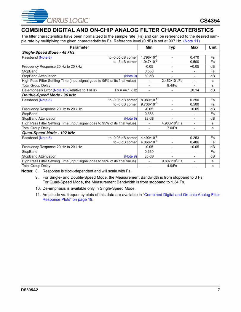
COMBINED DIGITAL AND ON-CHIP ANALOG FILTER CHARACTERISTICSThe filter characteristics have been normalized to the sample rate (Fs) and can be referenced to the desired sam-ple rate by multiplying the given characteristic by Fs. Reference level (0 dB) is set at 997 Hz. (Note 11)
Notes: 8. Response is clock-dependent and will scale with Fs.
9. For Single- and Double-Speed Mode, the Measurement Bandwidth is from stopband to 3 Fs. For Quad-Speed Mode, the Measurement Bandwidth is from stopband to 1.34 Fs.
10. De-emphasis is available only in Single-Speed Mode.
11. Amplitude vs. frequency plots of this data are available in “Combined Digital and On-chip Analog FilterResponse Plots” on page 19.
Parameter Min Typ Max UnitSingle-Speed Mode - 48 kHzPassband (Note 8) to -0.05 dB corner
to -3 dB corner1.796•10-4
1.947•10-5--
0.4700.500
FsFs
Frequency Response 20 Hz to 20 kHz -0.05 - +0.05 dBStopBand 0.550 - - FsStopBand Attenuation (Note 9) 80 dB - - dBHigh Pass Filter Settling Time (input signal goes to 95% of its final value) - 2.452•104/Fs - sTotal Group Delay - 9.4/Fs - sDe-emphasis Error (Note 10)(Relative to 1 kHz) Fs = 44.1 kHz - - ±0.14 dB
Double-Speed Mode - 96 kHzPassband (Note 8) to -0.05 dB corner
to -3 dB corner8.980•10-5
9.736•10-6--
0.2900.500
FsFs
Frequency Response 20 Hz to 20 kHz -0.05 - +0.05 dBStopBand 0.583 - - FsStopBand Attenuation (Note 9) 82 dB - - dBHigh Pass Filter Settling Time (input signal goes to 95% of its final value) - 4.903•104/Fs - sTotal Group Delay - 7.0/Fs - s
Quad-Speed Mode - 192 kHzPassband (Note 8) to -0.05 dB corner
to -3 dB corner4.490•10-5
4.868•10-6--
0.2530.486
FsFs
Frequency Response 20 Hz to 20 kHz -0.05 - +0.05 dBStopBand 0.630 - - FsStopBand Attenuation (Note 9) 85 dB - - dBHigh Pass Filter Settling Time (input signal goes to 95% of its final value) - 9.807•104/Fs - sTotal Group Delay - 4.9/Fs - s
DS895A2 7

CS4354
SWITCHING SPECIFICATIONS - SERIAL AUDIO INTERFACE
12. Not all sample rates are supported for all clock ratios. See Section 4.2 “Sample Rate Range/OperationalMode Detect” on page 13 for supported ratios and frequencies. SSM = Single-Speed Mode,DSM = Double-Speed Mode, QSM = Quad-Speed Mode.
13. SCLK period is defined by the SCLK / LRCK ratio. The SCLK / LRCK ratio may be either 32, 48, or 64.See Table 5 on page 14.
14.
Parameters Symbol Min Typ Max Units
MCLK Frequency 7.6 - 55.3 MHz
MCLK Duty Cycle 45 - 55 %
Input Sample Rate All MCLK/LRCK ratios combined(Note 12) (SSM) 256x, 384x, 512x, 768x, 1024x
(DSM) 128x, 192x, 256x, 384x, 512x(QSM) 128x, 192x, 256x
Fs 303084
170
----
21654
108216
kHzkHzkHzkHz
External SCLK Mode
LRCK Duty Cycle 45 - 55 %
SCLK Pulse Width Low tsclkl 20 - - ns
SCLK Pulse Width High tsclkh 20 - - ns
SCLK Duty Cycle 45 - 55 %
SCLK rising to LRCK edge delay tslrd 20 - - ns
LRCK edge to SCLK rising delay tslrs 20 - - ns
SDIN valid to SCLK rising setup time tsdlrs 20 - - ns
SCLK rising to SDIN hold time tsdh 20 - - ns
Internal SCLK Mode
LRCK Duty Cycle- -
SCLK Period (Note 13) tsclkw - - ns
MCLK falling to LRCK edge tmclkf - ns
LRCK edge to SCLK rising tsclkr - (Note 14) - ns
SDIN valid to SCLK rising setup time tsdlrs - - ns
SCLK rising to SDIN hold timeMCLK / LRCK = 1024, 512, 256, 128
tsdh
- -
ns
MCLK / LRCK = 768, 384, 192 - -
50%1
2 MCLK----------------------------– 50% 1
2 MCLK----------------------------+
109
SCLK----------------
109–4 MCLK---------------------------
109
4 MCLK---------------------------
109
512 Fs----------------------- 10+
109
512 Fs----------------------- 15+
109
384 Fs----------------------- 15+
tsclkr
tsclkw2
----------------- 109
2 MCLK--------------------------- tmclkf+ +=
8 DS895A2

CS4354
Figure 1. External Serial Clock Mode Input Timing
Figure 2. Internal Serial Clock Mode Input Timing
Figure 3. Internal Serial Clock Generation
sclkhtslrst
slrdt
sdlrst sdht
sclklt
SDIN
SCLK
LRCK
SDIN
*
LRCK
MCLK
tmclkf
sclkrt
sdhtsdlrst
INTERNAL SCLK
sclkwt
The SCLK pulses shown are internal to the CS4354.
SDIN
LRCK
MCLK
*INTERNAL SCLK
1 N2
N
* The SCLK pulses shown are internal to the CS4354. N equals MCLK divided by SCLK
DS895A2 9

CS4354
DIGITAL INTERFACE CHARACTERISTICSTest conditions (unless otherwise specified): GND = 0 V; all voltages with respect to ground.
INTERNAL POWER-ON RESET THRESHOLD VOLTAGESTest conditions (unless otherwise specified): GND = 0 V; all voltages with respect to ground.
Table 1. Power-On Reset Threshold Voltages
Figure 4. Power-On Reset Threshold Sequence
Parameters Symbol Min Typ Max UnitsHigh-Level Input Voltage 1.8 V <VL 5.0 V VIH 0.7xVL - - V
Low-Level Input Voltage 1.8 V <VL 5.0 V VIL - - 0.3xVL V
Input Leakage Current Iin - - ±10 A
Input Capacitance - 8 - pF
Parameters Symbol Min Typ Max Units
Internal Reset Asserted at Power-On Von1 - 0.2 - V
Internal Reset Released at Power-On Von2 - 3.6 - V
Internal Reset Asserted at Power-Off Voff - 3.1 - V
VA
Von2
Von1
Voff
GND
HI
LO
No Powerreset
undefinedresetactive
DAC Ready
resetactive
reset(internal)
10 DS895A2

CS4354
DC ELECTRICAL CHARACTERISTICSTest conditions (unless otherwise specified): VA = 5 V, VL = 3.3 V; GND = 0 V; SDIN = 0; all voltages with respect to ground.
Notes: 15. Power supply current increases with increasing sample rate and increasing MCLK frequency. Typicalvalues are based on Fs = 48 kHz and MCLK = 12.288 MHz. Maximum values are based on highestsample rate and highest MCLK frequency; see Switching Specifications - Serial Audio Interface. Vari-ance between speed modes is small.
16. During normal operation, SDIN = 997 Hz sine wave at 0 dBFS with load resistance RL = 3 k.
17. Power-down is defined as all clock and data lines held static low. All digital inputs have a weak pull-down (approximately 50 k) which is only present during power on reset. Opposing this pull-down willincrease the power-down current.
18. Valid with the recommended capacitor values as shown in the typical connection diagram in Section 5.
2.1 Digital I/O Pin Characteristics
Input and output levels and associated power supply voltage are shown in Table 2. Logic levels should notexceed the corresponding power supply voltage.
Table 2. Digital I/O Pin Characteristics
Parameters Symbol Min Typ Max Units
Power Supplies Power Supply Current (Note 15) Normal Operation (Note 16)
Power-Down (Note 17)
IVAIVLIVAIVL
----
100.10.51
130.2--
mAmAmAA
Power Dissipation (All Supplies) Normal Operation (Note 16)(Note 15) Power-Down (Note 17)
--
502.5
65-
mWmW
Power Supply Rejection Ratio (Note 18) (1 kHz)(60 Hz)
PSRR --
6060
--
dBdB
DC Output Voltages Pin Voltage FILT+ to GND
FLYP to FLYNGND to -VFILT
---
3.54.94.7
---
VVV
Pin Name Power Supply I/O Driver Receiver
MCLK VL Input - 1.8 V - 5 V
LRCK VL Input - 1.8 V - 5 V
SCLK VL Input - 1.8 V - 5 V
SDIN VL Input - 1.8 V - 5 V
DS895A2 11

CS4354
3. TYPICAL CONNECTION DIAGRAM
VL+1.8 V to +5 V
LRCK
MCLK
SCLK/DEM
SDIN
-VFILT
AOUTA
VA
470
2.2 nF
Rext
Rext
Line Level OutLeft & Right
Digital Audio Processor
Capacitors must be C0G or equivalent.
470
2.2 nFAOUTB
FILT+
FLYN
FLYP
2.2 µF
0.1 µF
+5 V
0.1 µF
Note 1:
GND2.2 µF
2.2 µF
2.2 µF
Note 1
1
5
3
4
2
6
7
11
14
9
8
13
12
10
+
+
+
+
GND
CS4354
Figure 5. Typical Connection Diagram
12 DS895A2

CS4354
4. APPLICATIONS
4.1 Ground-Centered Line Outputs
An on-chip charge pump creates a negative supply which allows the full-scale output swing to be centeredaround ground. This eliminates the need for large DC-blocking capacitors which create audible pops at pow-er-on and provides improved low frequency response. See the DAC Analog Characteristics table for thecomplete specifications of the full-scale output voltage. It should be noted that external output impedancebetween the AOUTx pin and the load will lower the voltage delivered to the load.
4.2 Sample Rate Range/Operational Mode Detect
The CS4354 operates in one of three operational modes. The device will auto-detect the correct mode whenthe input sample rate (Fs), defined by the LRCK frequency, falls within one of the ranges illustrated inTable 3. Sample rates outside the specified range for each mode are not supported. In addition to a validLRCK frequency, a valid serial clock (SCLK) and master clock (MCLK) must also be applied to the devicefor speed mode auto-detection; see Figure 9.
Table 3. CS4354 Operational Mode Auto-Detect
4.3 System Clocking
The device requires external generation of the master (MCLK), left/right (LRCK) and serial (SCLK) clocks.The left/right clock, defined also as the input sample rate (Fs), must be synchronously derived from theMCLK signal according to specified ratios. The specified ratios of MCLK to LRCK, along with several stan-dard audio sample rates and the required MCLK frequency, are illustrated in Table 4 on page 13.
Refer to Section 4.6 for the required SCLK timing associated with the selected Digital Interface Format andto “Switching Specifications - Serial Audio Interface” on page 8 for the maximum allowed clock frequencies.
Table 4. Common MCLK and LRCK Frequencies
Input Sample Rate (Fs) Mode30 kHz - 54 kHz Single-Speed Mode
84 kHz - 108 kHz Double-Speed Mode170 kHz - 216 kHz Quad-Speed Mode
LRCK(kHz)
MCLK (MHz)
128x 192x 256x 384x 512x 768x 1024x32 - - 8.1920 12.2880 16.3840 24.5760 32.7680
44.1 - - 11.2896 16.9344 22.5792 33.8688 45.158048 - - 12.2880 18.4320 24.5760 36.8640 49.1520
88.2 11.2896 16.9344 22.5792 33.8688 45.1584 - -96 12.2880 18.4320 24.5760 36.8640 49.1520 - -
176.4 22.5792 33.8688 45.1584 - - - -192 24.5760 36.8640 49.1520 - - - -
Mode QSM DSM SSM
DS895A2 13

CS4354
4.4 Serial Clock
The serial clock controls the shifting of data into the input data buffers. The CS4354 supports both externaland internal serial clock generation modes. Refer to Figure 6 for a diagram of the I²S data format.
In order to support selectable de-emphasis without a dedicated pin, pin 5 (SCLK/DEM) functions both asa serial clock input and a de-emphasis select. In typical applications where de-emphasis is not required,the SCLK/DEM pin is the input for an external serial clock - this is known as the External Serial ClockMode. To enable de-emphasis selection, the Internal Serial Clock Mode has to be used. Sections 4.4.1and 4.4.2 describe this feature in detail.
4.4.1 External Serial Clock Mode
The CS4354 will enter the External Serial Clock Mode when 16 low to high transitions are detected on theDEM/SCLK pin during any phase of the LRCK period. When this mode is enabled, the Internal SerialClock Mode and de-emphasis filter are disabled (see Figure 9 for flow diagram).
In the External Serial Clock Mode, the CS4354 will support I²S data up to 24-bit, with data valid on therising edge of SCLK.
4.4.2 Internal Serial Clock Mode
The CS4354 will switch to Internal Serial Clock Mode if no low to high transitions are detected on theDEM/SCLK pin for 2 consecutive frames of LRCK (see Figure 9 for flow diagram). In the Internal SerialClock Mode, the serial clock is internally derived and synchronous with MCLK and LRCK. TheSCLK/LRCK frequency ratio is either 32, 48, or 64 depending on the speed mode and MCLK frequency.Operation in this mode is identical to operation with an external serial clock synchronized with LRCK. Thismode allows access to the digital de-emphasis function. Refer to Table 5 for details (all frequencies listedas multiples of LRCK frequency).
Table 5. Internal SCLK Frequencies
4.4.2.1 De-Emphasis Control
The device includes on-chip digital de-emphasis. Figure 7 shows the de-emphasis curve for Fs equal to44.1 kHz. The frequency response of the de-emphasis curve scales with changes in the sample rate, Fs.The de-emphasis error will increase for sample rates other than 44.1 kHz.
When the SCLK/DEM pin is connected to VL (internal SCLK mode), the 44.1 kHz de-emphasis filter isactivated. When the SCLK/DEM pin is connected to GND, the de-emphasis filter is disabled. For moreinformation see “Internal Serial Clock Mode” on page 14.
Speed Mode MCLK = 128x 192x 256x 384x 512x 768x 1024xSSM - - 64x 48x 64x 64x 64xDSM - 48x - - - - -QSM - 32x 32x - - - -
LRCK
SCLK
Left Channel Right Channel
SDIN +3 +2 +1+5 +4MSB -1 -2 -3 -4 -5 +3 +2 +1+5 +4-1 -2 -3 -4MSBLSB LSB
Figure 6. CS4354 Data Format (I²S)
14 DS895A2

CS4354
De-emphasis selection is disabled in the external SCLK mode.
Note: De-emphasis is only available in Single-Speed Mode.
4.5 Internal High-Pass Filter
The CS4354 includes an internal digital high-pass filter. This filter prevents a constant digital offset from cre-ating a DC voltage on the analog output pins. The filter’s corner frequency is well below the audio band; see“Switching Specifications - Serial Audio Interface” on page 8 for filter specifications.
4.6 Digital Interface Format
The device accepts audio samples in the industry standard I²S format only.
For an illustration of the required relationship between the LRCK, SCLK and SDIN, see Figure 6 on page14. SDIN is valid on the rising edge of SCLK. For more information about serial audio formats, refer to CirrusLogic Application Note AN282: The 2-Channel Serial Audio Interface: A Tutorial, available at http://www.cir-rus.com.
4.7 Internal Power-On Reset
The CS4354 features an internal power-on reset (POR) circuit. This circuit monitors the VA supply and au-tomatically asserts or releases an internal reset of the DAC’s digital circuitry when the supply reaches de-fined thresholds (see “Internal Power-On Reset Threshold Voltages” on page 10). No external clocks arerequired for the POR circuit to function.
Figure 8. Internal Power-On Reset Circuit
When power is first applied, the POR circuit monitors the VA supply voltage to determine when it reachesa defined threshold, Von1. At this time, the POR circuit asserts the internal reset low, resetting all of the
GaindB
-10dB
0dB
Frequency
T2 = 15 µs
T1=50 µs
F1 F23.183 kHz 10.61 kHz
Figure 7. De-Emphasis Curve, Fs = 44.1 kHz
Power-On Reset Circuit
VA
GND
reset(internal)
DS895A2 15
CS4354
digital circuitry. Once the VA supply reaches the secondary threshold, Von2, the POR circuit releases theinternal reset.
When power is removed and the VA voltage reaches a defined threshold, Voff, the POR circuit asserts theinternal reset low, resetting all of the digital circuitry.
Note: For correct operation of the internal POR circuit, the voltage on VL must rise before or simulta-neously with VA.
4.8 Initialization
When power is first applied, the DAC enters a reset (low power) state at the beginning of the initializationsequence. In this state, the AOUTx pins are weakly pulled to ground and FILT+ is connected to GND.
The device will remain in the reset state until VON2 is reached. Once VON2 is reached, the internal digitalcircuitry is reset and the DAC enters a power-down state until MCLK is applied.
Once MCLK is valid, the device enters an initialization state in which the charge pump powers up and charg-es the capacitors for the negative voltage supply.
Once LRCK is valid, the number of MCLK cycles is counted relative to the LRCK period to determine theMCLK/LRCK frequency ratio. Next, the device enters the power-up state in which the interpolation filtersand delta-sigma modulators are turned on, the internal voltage reference, FILT+, powers up to normal op-eration, the analog output pull-down resistors are removed, and power is applied to the output amplifiers.
If a valid SCLK is applied, the device will clock in data according to the applied SCLK. If no SCLK is present,the device will clock in data using the derived internal SCLK (see Figure 3 on page 9) and will apply the de-emphasis filter according to Section 4.4.2.1 on page 14.
After this power-up state sequence is complete, normal operation begins and analog output is generated.
If valid MCLK, LRCK, and SCLK are applied to the DAC before VON2 is reached, the total time from VON2to the analog audio output from AOUTx is less than 50 ms.
See Figure 9 for a diagram of the device’s states and transition conditions.
16 DS895A2

CS4354
USER: Apply Power
USER: Apply MCLK
MCLK/LRCK Ratio Detection
USER: Apply LRCK
Power-On Reset State
Power-Down State
Initialization State
Power-Up State
Valid MCLK/LRCK Ratio
Outputs Muted
USER: Change MCLK/LRCK ratio
USER:Remove MCLK
USER: Applied SCLK
SCLK mode = internal SCLK mode = external
Normal OperationDe-emphasisIs Selectable
Analog Outputis Generated
Normal OperationDe-emphasisIs Disabled
USER: No SCLK
Mute State
USER: Change MCLK/LRCK ratioValid MCLK/LRCK Ratio
Figure 9. Initialization and Power-Down Sequence Diagram
DS895A2 17

CS4354
4.9 Recommended Power-Up and Power-Down Sequences
4.9.1 Power-Up Sequence
Follow the power-up sequence below:
1. Apply power.
2. After the power supplies are stable, provide the correct MCLK, LRCK, and SCLK (only in External Serial Clock Mode) signals to progress from the ‘Power-Down State’ in the power-up sequence seen in Figure 9. Please refer to Section 4.4 on page 14 for common clock frequencies in the External Serial Clock Mode, and supported modes in the Internal Serial Clock Mode. The sequence will complete and audio will be output from the AOUTx pins within 50 ms after valid clocks are applied.
4.9.2 Power-Down Sequence
Follow the power-down sequence below:
1. For minimal pops, set the input digital data (SDIN) to zero for at least 8192 consecutive samples.
2. Remove the MCLK signal without applying any glitched pulses to the MCLK pin.
3. Remove the power supply voltages.
Note: A glitched pulse is any pulse that is shorter than the period defined by the minimum/maximumMCLK signal duty cycle specification and the nominal frequency of the input MCLK signal. A transient mayoccur on the analog outputs if the MCLK signal duty cycle specification is violated when the MCLK signalis removed during normal operation; see “Switching Specifications - Serial Audio Interface” on page 8.
4.10 Grounding and Power Supply Arrangements
As with any high-resolution converter, the CS4354 requires careful attention to power supply and groundingarrangements if its potential performance is to be realized. The “Typical Connection Diagram” on page 12shows the recommended power arrangements with VA and VL connected to clean supplies. It is stronglyrecommended that a single ground plane be used with the GND pins connected to the common plane; thisis important because both pin 6 and pin 10 provide analog ground reference to the CS4354. Should it benecessary to split the ground planes, the CS4354 should be placed entirely in the analog plane. In this con-figuration, it is critical that the digital and analog ground planes be tied together with a low-impedance con-nection, ideally a strip of copper on the printed circuit board, at a single point near the CS4354.
All signals, especially clocks, should be kept away from the FILT+ pin in order to avoid unwanted couplinginto the DAC.
4.10.1 Capacitor Placement
Decoupling capacitors should be placed as close to the device as possible, with the low-value ceramiccapacitor being the closest. To further minimize impedance, these capacitors should be located on thesame PCB layer as the device. See DC Electrical Characteristics for the voltage present across pin pairs.This is useful for choosing appropriate capacitor voltage ratings and orientation if electrolytic capacitorsare used.
The CDB4354 evaluation board demonstrates the optimum layout and power supply arrangements.
18 DS895A2

CS4354
5. COMBINED DIGITAL AND ON-CHIP ANALOG FILTER RESPONSE PLOTS
0.4 0.5 0.6 0.7 0.8 0.9 1−120
−100
−80
−60
−40
−20
0
Single−Speed Stopband Rejection
Frequency(normalized to Fs)
Am
plitu
de(d
B)
0.4 0.42 0.44 0.46 0.48 0.5 0.52 0.54 0.56 0.58 0.6−120
−100
−80
−60
−40
−20
0
Single−Speed Transition Band
Frequency(normalized to Fs)
Am
plitu
de(d
B)
Figure 10. Single-Speed Stopband Rejection Figure 11. Single-Speed Transition Band
0.45 0.46 0.47 0.48 0.49 0.5 0.51 0.52 0.53 0.54 0.55−10
−9
−8
−7
−6
−5
−4
−3
−2
−1
0Single−Speed Transition Band Detail
Frequency(normalized to Fs)
Am
plitu
de(d
B)
0 0.05 0.1 0.15 0.2 0.25 0.3 0.35 0.4 0.45 0.5−0.06
−0.04
−0.02
0
0.02
0.04
0.06Single−Speed Passband Ripple
Frequency(normalized to Fs)
Am
plitu
de(d
B)
Figure 12. Single-Speed Transition Band (detail) Figure 13. Single-Speed Passband Ripple
0.4 0.5 0.6 0.7 0.8 0.9 1−120
−100
−80
−60
−40
−20
0
Double−Speed Stopband Rejection
Frequency(normalized to Fs)
Am
plitu
de(d
B)
0.4 0.42 0.44 0.46 0.48 0.5 0.52 0.54 0.56 0.58 0.6−120
−100
−80
−60
−40
−20
0
Double−Speed Transition Band
Frequency(normalized to Fs)
Am
plitu
de(d
B)
Figure 14. Double-Speed Stopband Rejection Figure 15. Double-Speed Transition Band
DS895A2 19

CS4354
0.45 0.46 0.47 0.48 0.49 0.5 0.51 0.52 0.53 0.54 0.55−10
−9
−8
−7
−6
−5
−4
−3
−2
−1
0Double−Speed Transition Band Detail
Frequency(normalized to Fs)
Am
plitu
de(d
B)
0 0.05 0.1 0.15 0.2 0.25−0.2
−0.15
−0.1
−0.05
0
0.05
0.1
0.15
0.2Double−Speed Passband Ripple
Frequency(normalized to Fs)
Am
plitu
de(d
B)
Figure 16. Double-Speed Transition Band (detail) Figure 17. Double-Speed Passband Ripple
0.2 0.3 0.4 0.5 0.6 0.7 0.8 0.9 1−120
−100
−80
−60
−40
−20
0
Quad−Speed Stopband Rejection
Frequency(normalized to Fs)
Am
plitu
de(d
B)
0.2 0.3 0.4 0.5 0.6 0.7 0.8−120
−100
−80
−60
−40
−20
0
Quad−Speed Transition Band
Frequency(normalized to Fs)
Am
plitu
de(d
B)
Figure 18. Quad-Speed Stopband Rejection Figure 19. Quad-Speed Transition Band
0.45 0.46 0.47 0.48 0.49 0.5 0.51 0.52 0.53 0.54 0.55−10
−9
−8
−7
−6
−5
−4
−3
−2
−1
0Quad−Speed Transition Band Detail
Frequency(normalized to Fs)
Am
plitu
de(d
B)
0 0.05 0.1 0.15 0.2 0.25 0.3 0.35 0.4−0.2
−0.15
−0.1
−0.05
0
0.05
0.1
0.15
0.2Quad−Speed Passband Ripple
Frequency(normalized to Fs)
Am
plitu
de(d
B)
Figure 20. Quad-Speed Transition Band (detail) Figure 21. Quad-Speed Passband Ripple
20 DS895A2

CS4354
6. PARAMETER DEFINITIONS
Total Harmonic Distortion + Noise (THD+N)
The ratio of the RMS value of the signal to the RMS sum of all other spectral components over the specifiedbandwidth (typically 10 Hz to 20 kHz), including distortion components. Expressed in decibels.
Dynamic Range
The ratio of the full-scale RMS value of the signal to the RMS sum of all other spectral components over thespecified bandwidth. Dynamic range is a signal-to-noise measurement over the specified bandwidth madewith a -60 dBFS signal. 60 dB is then added to the resulting measurement to refer the measurement to fullscale. This technique ensures that the distortion components are below the noise level and do not affect themeasurement. This measurement technique has been accepted by the Audio Engineering Society, AES17-1991, and the Electronic Industries Association of Japan, EIAJ CP-307.
Interchannel Isolation
A measure of crosstalk between the left and right channels. Measured for each channel at the converter'soutput with all zeros to the input under test and a full-scale signal applied to the other channel. Units in deci-bels.
Interchannel Gain Mismatch
The gain difference between left and right channels. Units in decibels.
Gain Drift
The change in gain value with temperature. Units in ppm/°C.
DS895A2 21

CS4354
7. PACKAGE INFORMATION
7.1 Dimensions
7.2 Thermal Characteristics
INCHES MILLIMETERSDIM MIN NOM MAX MIN NOM MAX
A 0.0590 - 0.0708 1.397 - 1.549A1 0.0040 - 0.0098 0.102 - 0.249b 0.0138 - 0.0200 0.351 - 0.508C 0.0075 - 0.0098 0.190 - 0.250D 0.3380 - 0.3440 8.585 - 8.738E 0.1520 - 0.1574 3.861 - 3.998e - 0.050 BSC - - 1.270 BSC -H 0.2300 - 0.2440 5.842 - 6.198L 0.0160 - 0.0350 0.406 - 0.889 0° - 8° 0° - 8°
JEDEC #: MS-012
Controling Dimension is Millimeters
Parameter Symbol Min Typ Max Units
Junction to Ambient Thermal Impedance 2 Layer Board4 Layer Board
JA --
11086
--
°C/Watt
e
14L SOIC (150 MIL BODY) PACKAGE DRAWING
D
HE
b
A1
A
c
L
SEATINGPLANE
1
22 DS895A2

CS4354
8. ORDERING INFORMATION
Product Description Package Pb-Free Grade Temp Range Container Order #
CS43545 V Stereo Audio DAC
with 2 VRMS Line Output14-pin SOIC
YES Commercial -40° to +85° CRail CS4354-CSZ
Tape & Reel CS4354-CSZRCDB4354 CS4354 Evaluation Board - - - - CDB4354
DS895A2 23

CS4354
9. REVISION HISTORY
Release ChangesA1 (Sept ‘09) – Initial release.
A2 (July ‘10)
– Updated THD+N specification in DAC Analog Characteristics.– Updated dynamic range specification in DAC Analog Characteristics.– Updated idle channel noise/SNR specification in DAC Analog Characteristics.– Updated front page dynamic range and THD+N performance to match updated specifications.– Updated frequency response specification description in Combined Digital and On-Chip Analog Filter
Characteristics so that frequency response limits are measured relative to 1 kHz.– Updated Power On Reset threshold values in Internal Power-On Reset Threshold Voltages.– Removed typical specification for LRCK and SCLK in Switching Specifications - Serial Audio Interface.– Updated power supply current specifications in DC Electrical Characteristics.– Updated pin voltage specification in DC Electrical Characteristics.– Corrected MCLK frequency in Table 4 from 33.8680 MHz to 33.8688 MHz.– Updated test condition bandwidth in DAC Analog Characteristics from 10 Hz - 20kHz to 20 Hz - 20kHz– Removed MCLK = 1152x LRCK mode support (per Rev B0 silicon). Updated specifications (LRCK min and
corresponding MCLK min) in Switching Specifications - Serial Audio Interface, and applications information in Table 4 and Table 5.
– Added (Note 16) to DC Electrical Characteristics.– Updated FILT+ description in Initialization.– Updated interchannel isolation specification in DAC Analog Characteristics.– Updated Table 3 to match specifications in Switching Specifications - Serial Audio Interface.– Removed High Pass Filter Characteristics section; appended updated specifications to Combined Digital
and On-Chip Analog Filter Characteristics.– Updated passband and stopband specifications in Combined Digital and On-Chip Analog Filter
Characteristics to reflect Rev B0 silicon.– Updated title and plots in Combined Digital and On-chip Analog Filter Response Plots to reflect Rev B0
silicon.– Updated typical output offset in DAC Analog Characteristics.– Updated timing diagram Figure 2 to reflect internal SCLK generation as shown in Figure 3.– Updated Typical Connection Diagram; VL capacitor now recommended by default.
24 DS895A2

CS4354
Contacting Cirrus Logic SupportFor all product questions and inquiries, contact a Cirrus Logic Sales Representative. To find one nearest you, go to www.cirrus.com.
IMPORTANT NOTICE
“Advance” product information describes products that are in development and subject to development changes. Cirrus Logic, Inc. and its subsidiaries (“Cirrus”) be-lieve that the information contained in this document is accurate and reliable. However, the information is subject to change without notice and is provided “AS IS”without warranty of any kind (express or implied). Customers are advised to obtain the latest version of relevant information to verify, before placing orders, thatinformation being relied on is current and complete. All products are sold subject to the terms and conditions of sale supplied at the time of order acknowledgment,including those pertaining to warranty, indemnification, and limitation of liability. No responsibility is assumed by Cirrus for the use of this information, including useof this information as the basis for manufacture or sale of any items, or for infringement of patents or other rights of third parties. This document is the property ofCirrus and by furnishing this information, Cirrus grants no license, express or implied under any patents, mask work rights, copyrights, trademarks, trade secrets orother intellectual property rights. Cirrus owns the copyrights associated with the information contained herein and gives consent for copies to be made of the infor-mation only for use within your organization with respect to Cirrus integrated circuits or other products of Cirrus. This consent does not extend to other copying suchas copying for general distribution, advertising or promotional purposes, or for creating any work for resale.
CERTAIN APPLICATIONS USING SEMICONDUCTOR PRODUCTS MAY INVOLVE POTENTIAL RISKS OF DEATH, PERSONAL INJURY, OR SEVERE PROP-ERTY OR ENVIRONMENTAL DAMAGE (“CRITICAL APPLICATIONS”). CIRRUS PRODUCTS ARE NOT DESIGNED, AUTHORIZED OR WARRANTED FOR USEIN PRODUCTS SURGICALLY IMPLANTED INTO THE BODY, AUTOMOTIVE SAFETY OR SECURITY DEVICES, LIFE SUPPORT PRODUCTS OR OTHER CRIT-ICAL APPLICATIONS. INCLUSION OF CIRRUS PRODUCTS IN SUCH APPLICATIONS IS UNDERSTOOD TO BE FULLY AT THE CUSTOMER’S RISK AND CIR-RUS DISCLAIMS AND MAKES NO WARRANTY, EXPRESS, STATUTORY OR IMPLIED, INCLUDING THE IMPLIED WARRANTIES OF MERCHANTABILITY ANDFITNESS FOR PARTICULAR PURPOSE, WITH REGARD TO ANY CIRRUS PRODUCT THAT IS USED IN SUCH A MANNER. IF THE CUSTOMER OR CUSTOM-ER’S CUSTOMER USES OR PERMITS THE USE OF CIRRUS PRODUCTS IN CRITICAL APPLICATIONS, CUSTOMER AGREES, BY SUCH USE, TO FULLYINDEMNIFY CIRRUS, ITS OFFICERS, DIRECTORS, EMPLOYEES, DISTRIBUTORS AND OTHER AGENTS FROM ANY AND ALL LIABILITY, INCLUDING AT-TORNEYS’ FEES AND COSTS, THAT MAY RESULT FROM OR ARISE IN CONNECTION WITH THESE USES.
Cirrus Logic, Cirrus, and the Cirrus Logic logo designs are trademarks of Cirrus Logic, Inc. All other brand and product names in this document may be trademarksor service marks of their respective owners.
Blu-Ray Disc is a registered trademark of SONY KABUSHIKI KAISHA CORPORATION.
DS895A2 25