5-4 ultra-fast optical processing technology and its
TRANSCRIPT

1 Introduction
In the next generation optical network,high scalability and fine granularity will bestrongly required in addition to broadband.Wavelength division multiplexing (WDM)technology has enabled broadband data trans-mission [1]. However, the granularity of aWDM light-path network is coarse. AlthoughInternet protocol (IP) over generalized multi-protocol label switching (GMPLS) over WDMapproach provides a fine granularity [2], itsslower electronic processing, such as memoryaccess for header analysis at IP routers, will bea bottleneck of a network. Optical processingtechnologies are needed for high-speed pro-cessing for broadband photonic network. Wehave proposed and experimentally demon-strated optical packet switching (OPS) net-works based on optical label (i.e. code) pro-cessing, such as header analysis and labelswapping [3][4]. Optical processing basedOPS networks can provide high scalability,fine granularity and ultra high-speed hopping.Recently, in spite of immatureness of opticaltechnology, many OPS systems have been
developed because of its big merit [5]-[8].Recently, we have developed 40 Gbit/s inter-face, all-optical label processing based OPSprototype with optical switch, optical buffer,and electronic scheduler [8]. This is the firstOPS prototype with ultra-fast functions suchas optical address-table lookup and transparentoptical buffering.
An optical packet consists of a header anda payload data. The header has an opticalcode-based label [3][4][8][9][10][12] represent-ing a destination node. In the label processor,a packet header label is analyzed all optically.All-optical label processing methods are rep-resented in Fig. 1. We have investigated threedifferent label-processing methods: (a) plan-ner lightwave circuits (PLC) based correlatorswith binary phase shift keying (BPSK) codelabel [3][8], (b) multi-section fiber Bragg grat-ing (FBG) based correlators with multi-wave-length label [4], and (c) a holographic multiplecorrelator with on-off keying (OOK) or BPSKlabel [9][10][12].In methods (a) and (b), a set ofoptical correlators works as a label bank,which holds optical labels correspond to thedestination addresses in the routing table.
WADA Naoya and KUBOTA Fumito 151
5-4 Ultra-fast Optical Processing Technologyand its Application to Photonic Network
WADA Naoya and KUBOTA Fumito
Ultra-high speed all-optical label processing methods are proposed and experimentallydemonstrated.These methods dramatically increase the label processing capability. Opticalpacket switch (OPS) systems and networks based on OPS nodes are expressed as an appli-cation of optical processing technologies. First 40 Gbit/s/port OPS prototype with all-opticallabel processor, optical switch, optical buffer, and electronic scheduler is expressed. Thefeasibility of OPS networks is verified by experimental demonstrations.
Keywords Networks, Optical communications, Optical label processing, Optical packet switch-ing, Prototype

152
Label recognition is based on parallel opticalcorrelation in the time and/or frequencydomain between an input optical label andlabels in the label bank. In the method (c), anangular multiplexed spectral hologram(AMSH) is used as a multiple correlator forinput labels. An AMSH holds many opticallabels correspond to the destination addressesand outputs correlation signals toward differ-ent angles due to input labels.
2 Optical code based label pro-cessing and switching
2.1 Network architecture and packetformat
Figure 2 (a) represents proposed photonicnetwork architecture. The network consists ofedge nodes, optical cross connects (OXC), andOPS nodes. Edge nodes are connected withthe local routers either in access networks orusers' premises. OPS nodes are located in thephotonic network as backbone routers. Thesepacket switches can communicate with eachother through OXC in core network. Packet-by-packet electrical processing is not per-formed. It will minimize transfer delay andsupport the high throughput of the nodes. Fig-
ure 2 (b) represents proposed optical packetformat. A packet consists of header and pay-load data. We are using 200 Gchip/s, 8-chip,optical BPSK code label as a packet headerinvolving a destination node address informa-tion. In the system, variable rate burst data isacceptable because of no O/E and E/O conver-sion to the data. To generate high-speed data,electric time domain multiplexing (ETDM) oroptical time domain multiplexing (OTDM)technology is introduced. In any data ratecases, chip rate of the label is not changed.These time domain multiplexing technologiesin OPS network is useful for making a shorterlength packet and enhancement of a networkscalability.
2.2 Label recognition and packetswitching
As described in previous sub-section, anoptical packet consists of a header and a data(see in Fig. 2(b)). The header has an opticalcode-based label of a destination node. In theOPS node, an optical packet is simply dividedinto two arms. In the label processing part, anoptical label processor analyzes a packet head-er optically. All-optical label recognitionmethod is represented in Fig. 3. In an optical
Journal of the National Institute of Information and Communications Technology Vol.51 Nos.1/2 2004
All-optical label processing methodsFig.1

label processor, a set of optical correlatorsworks as a label bank, which stores opticalcodes correspond to the destination addressesin the routing table. Label recognition isbased on parallel optical correlation in thetime domain between an input optical codeand the codes in the label bank. Each correla-tor decodes the input label of each packetheader and outputs the signal, which has highor low value at matched and unmatched cases,respectively. A high value signal opens a gate-switch of a destination port, while low valuesignals keep close other switches.
2.3 ExperimentsFigure 4 represents the experimental set-
up of distributed OPS with two ports. Set-upconsists of an optical packet transmitter andthe OPS composed of label processor, 1×2optical gate switch, and optical delay. Anoptical packet transmitter consists of 2 ps-10GHz-MLLD, LiNbO3 intensity modulators(IM), optical encoder, and optical delay. Opti-cal encoder consists of tapped delay-lines withthermo-controlled optical phase shifters asshown in Fig. 4. All elements are monolithi-cally integrated by using PLC technology.The optical carrier phase of each chip pulse isshifted either 0 orπby the phase shifter togenerate the 8-chip BPSK-codes [11]. Labelprocessor is comporsed of optical correlaters,photo detectors (PD), low-pass filters (LPF),and gate signal generator. The 1×2 opticalgate switch consists of two IMs with 40 GHzbandwidth.
In the optical packet transmitter shown inFig.4, IM 2 generates 64 bit-long packet datasignal at 10 Gbit/s. IM 1 and optical encodergenerate optical label which is 8-chip BPSKoptical codes with a time interval of 5 ps.Generated optical code and payload data sig-nal are combined to form a packet. In thelabel processor, if the input code matches withthe code of a correlater, the output (correlatedsignal) takes a high value. On the other hand,in unmatched case, the correlated signal takes
WADA Naoya and KUBOTA Fumito 153
(a) Network architecture and (b)packet format
Fig.2
All-optical parallel table look-upFig.3

154
lower value. In matched case, the correlationsignal is converted to the electrical signal andused to gate and hold open the IM gate switchvia gate signal generator. While in theunmatched case, the bias is not changed, thenthe gate switch still close. The label processorcan open an objective gate switch and routsthe matched packet to the target port.
Figure 5 (a) is a streak camera trace of agenerated packet with an optical code #1: “0ππππππ0”. Figure 5 (b) and (c) representstreak camera trace of correlater outputs to the
packets with a header of code #1: “0ππππππ0” (matched code) and a code #2: “0π0π0π0π” (unmatched code), respectively. In bothcases, each bit of payload data of the packet isspread in time domain by passing through thecorrelater and takes so small value in compari-son with the decoded label that it does notoperate mistakenly with gate switch.
Figure 6 (a) and (b) represent the meas-ured payload data of Port 1 and Port 2 to thetwo different input packet having label of “0ππππππ0” matched with correlater 1 and “0π
Journal of the National Institute of Information and Communications Technology Vol.51 Nos.1/2 2004
Experimental setupFig.4
Streak camera trace of (a) generated packet and correlated signals in (b) matched and(c) unmatched cases
Fig.5

0π0π0π” matched with correlater 2, respec-tively. These clearly show that the addressprocessor alternatively switches two opticalgate switches as the input optical code switch-es between #1 and #2. It means that the labelprocessor distinguish the 8-chip long opticalcodes label at the header of packets and con-trol the optical switch. Figure 7 (a) and (b) aremeasured bit error rates (BER) of routed64bit-long payload data with code #1 and #2,respectively, in each corresponding port. Themeasured BERs are less than 10-10, which con-firms the proper packet routing operation.Thses results guarantee the high speed OPSnetwork.
3 Multi-wavelength label pro-cessing and variable lengthpacket switching
3.1 Network architecture and packetformat
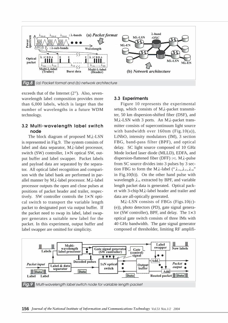
We introduce a novel packet format con-sisting of a header, a payload, and a trailer inFig.8 (a). The header has a label of a destina-tion node. The label is K chip-long, each ofwhich is one of W wavelengths. Figure 8 (a)represents a case of K=W=4. Here,λ1A,λ1B,λ
1C, andλ1D are used to generate multi-wave-length labels. Variable length payload datauses different wavelength,λ1E, from thoseused for label. The trailer is the same as theheader. Wavelengthsλ1A throughλ1E make awavelength bandλ1A-E. In each band, the samenumber of independent labels are generatedand used as a header and a trailer of packet.
Figure 8 (b) depicts the network architec-ture. It consists of multi-wavelength edgenode (Mλ-EN), multi-wavelength labelswitching node (Mλ-LSN), and wavelengthbased optical cross connect (λ-OXC). Mλ-ENgives multiple wavelengths as a label. Mλ-LSN recognizes the multi-wavelength label inoptical domain, and routes the packet toassigned port. Generation and recognition ofmulti-wavelength label are performed all-opti-cally by multi-section fiber Bragg gratings(MS-FBGs).λ-OXCs switch the band. (See [4]in detail.)
A network with the Mλ-LSNs recognizesmore optical label than aλ-LSN network. Thelabel composition gives W!/(W-K )! differentlabels to packets while the number of wave-lengths is W. This means that W!/(W-K )! Mλ-ENs can communicate with each other all-optically while W in theλ-LSN case. Forexample, assume that 16 wavelengths aregiven to the multi-wavelength label composi-tion. The number of labels of a network withMλ-LSNs is more than 4 billion, which
WADA Naoya and KUBOTA Fumito 155
Routed packet data with code (a) #1and (b) #2
Fig.6
Measured BER at (a) Port 1 and (b)Port 2
Fig.7
156
exceeds that of the Internet (232). Also, seven-wavelength label composition provides morethan 6,000 labels, which is larger than thenumber of wavelengths in a future WDMtechnology.
3.2 Multi-wavelength label switchnode
The block diagram of proposed Mλ-LSNis represented in Fig.9. The system consists oflabel and data separator, Mλ-label processor,switch (SW) controller, 1×N optical SW, out-put buffer and label swapper. Packet labelsand payload data are separated by the separa-tor. All optical label recognition and compari-son with the label bank are performed in par-allel manner by Mλ-label processor. Mλ-labelprocessor outputs the open and close pulses atpositions of packet header and trailer, respec-tively. SW controller controls the 1×N opti-cal switch to transport the variable lengthpacket to designated port via output buffer. Ifthe packet need to swap its label, label swap-per generates a suitable new label for thepacket. In this experiment, output buffer andlabel swapper are omitted for simplicity.
3.3 ExperimentsFigure 10 represents the experimental
setup, which consists of Mλ-packet transmit-ter, 50 km dispersion-shifted fiber (DSF), andMλ-LSN with 3 ports. An Mλ-packet trans-mitter consists of supercontinuum light sourcewith bandwidth over 160nm (Fig.10(a)),LiNbO3 intensity modulators (IM), 3 sectionFBG, band-pass filter (BPF), and opticaldelay. SC light source composed of 10 GHzMode locked laser diode (MLLD), EDFA, anddispersion-flattened fiber (DFF) [4]. Mλ-pulsefrom SC source divides into 3 pulses by 3 sec-tion FBG to form the Mλ-label (“λ1A,λ1C,λ1B”in Fig.10(b)). On the other hand pulse withwavelengthλ1E extracted by BPF, and variablelength packet data is generated. Optical pack-et with 3-chip Mλ-label header and trailer anddata are all-optically generated.
Mλ-LSN consists of FBGs (Figs.10(c)-(e)), photo detectors (PD), gate signal genera-tor (SW controller), BPF, and delay. The 1×3optical gate switch consists of three IMs with40 GHz bandwidth. The gate signal generatorcomposed of thresholder, limiting RF amplifi-
Journal of the National Institute of Information and Communications Technology Vol.51 Nos.1/2 2004
(a) Packet format and (b) network architectureFig.8
Multi-wavelength label switch node for variable length packetFig.9

er, and T-flip-flop. In the Mλ-LSN, FBGsplay the role in correlater and label bank. Ifthe input label is matched with theλ set of acorrelater, the output takes a high value. Oth-erwise, the correlated signal takes lower value.The correlation signals are converted to theelectrical pulse signals by PD. In matchedcase, a pulse at matched header label open theIM gate switch, and a pulse at matched trailerlabel close the switch. While in theunmatched case, the bias is not changed, thenthe gate switch keeps close. The label proces-sor can open an objective gate switch and leadthe matched variable length packet to the des-ignated port.
Figure 11(a) is the generated 64bit longpacket with header and trailer of Mλ-label:“λ1A,λ1C,λ1B”. Figure 11(b) and (c) representcorrelation outputs of FBG1* with aλset “λ1B,λ1C,λ1A” and FBG2* with aλset “λ1C,λ1B,λ1A”to the input label “λ1A,λ1C,λ1B”, respectively.In matched case (Fig.11(b)) correlation signalhas a high peak, while unmatched case(Fig.11(c)), the signal has no high peak. Thisis a demonstration of the all-optical Mλ-labelrecognition. Figure 11(d)-(f) represent theswitched payload data at Ports 1, 2, and 3 tothe three different length input packets; (d)64 bit data with label “λ1A,λ1C,λ1B” matchedwith FBG1*, (e) 128 bit data with label “λ1C,λ1B,λ1A” matched with FBG3*, and (f) 192 bitdata with label “λ1A,λ1B,λ1C” matched with
FBG2*, respectively. These clearly show thatthe Mλ-LSN can switch variable length pack-et, which depends on the input optical label.Figure 11(g) is measured BER at Port 1 incases of back-to-back and after 50 km trans-mission of three different length packet.These results guarantee the ultra-high speedOPS network using multi-wavelength labelprocessing.
4 Holographic label processingby AMSH
The angular multiplexing capability ofholograms has been shown for implementinglarge-scale parallel optical storage. We expectto reduce the number of correlator in an opti-cal label processor by using an angular-multi-plexed spectral hologram (AMSH) as anaddress bank [9]. The holographic labelprocessor is shown in Fig.12 (a). The holo-graphic label processor is composed of dif-fraction grating, Fourier transformation lensand AMSH. The label with destinationaddress information separates time and spatialaxis by the diffraction grating. This diffractedsignal passes through the Fourier transforma-tion lens and is incident on the spectral holo-gram as objective light. Some labels havebeen recorded in angle-multiplexed manner.The reconstructive light, which is produced byan AMSH, passes through the Fourier trans-
WADA Naoya and KUBOTA Fumito 157
Experimental setupFig.10

158
formation lens again and outputs as a correla-tion peak to the position depending upon theeach incidence label (see Fig. 12 (b) and (c)).The light detected by PD array. Address infor-mation in each label is detected as the positioninformation on the PD array. The signal acti-vates the optical gate switch to route the opti-
cal data packet to the designated port. In the spatial label recognition, it is neces-
sary to use the spatial patterns of signals. Sev-eral groups have reported all-optical time-to-space conversion techniques that entirely sep-arate the temporal and spatial axis. However,in our system, it is necessary not the complete
Journal of the National Institute of Information and Communications Technology Vol.51 Nos.1/2 2004
Experimental resultsFig.11
(a) Holographic label processor and measured intensity distribution at (b) Position 1 and(c) Position 2
Fig.12

time-to-space conversion pattern, but spatialpatterns reflect the temporal waveform of thesignal [10]. The individual frequency compo-nents contained within the incident signals areangularly dispersed by the diffraction grating,and then focused at the back focal plane of thelens, where the frequency components are spa-tially separated along one dimension. There-fore, we produce the AMSH by using spatiallydispersed optical Fourier components. Thislabel processing method is expressed in detailin a recent report [12].
5 40 Gbit/s interface OPS proto-type
5.1 Prototype architectureRecently, we have developed 40 Gbit/s
interface, all-optical code-label processingbased OPS prototype [8]. Figure 13 representsthe block diagram of the prototype. The pro-totype consists of optical label processor, opti-cal switche, electronic scheduler, and opticalbuffer. As parts of the prototype, we alsodeveloped optical packet transmitter withOTDM multiplexer and optical packet receiv-er with OTDM de-multiplexer for the per-formance analysis. An optical packet consists
of a header and a payload data as shown inFig. 13. The header has an optical code-labelrepresenting a destination node. In the labelprocessor, a packet header label is analyzed alloptically.
5.2 Label processing and switchingIn our OPS prototype, we introduce label
recognition method (a) in Fig.1. Label proces-sor controls the optical switch and gives pack-et arriving information to the buffer scheduler.By separating the individual functions of apacket switch, we can fully use all-opticallabel processing capability. The specificationof the prototype is represented in Table 1. Theprototype is a 2×2 packet switch. We assumethat packets arrive synchronously in order tosimplify buffer architecture. The packetlength is fixed. The inter-arrival time of thepackets at each port is a multiple of T, where Tis the time equivalent to the sum of the packetlength and guard time.
The optical packet transmitter generates 8-chip, 200 Gchip/s optical BPSK label and 40 Gbit/s, 16000 bit random burst data to forman optical packet. The waveform of generatedoptical packets is shown in Fig. 14(a). Thelabel processor consists of PLC correlatorsand optical switch driver. Table lookup of thepacket label is performed in a parallel mannerwithout O/E and E/O conversions [3] asdescribed in Section 2. In case of matchedlabel, the correlator outputs the autocorrela-tion waveform with high peak (Fig. 14(b)) andopens the target optical gate switch to routesthe packet to destination port. In case of
WADA Naoya and KUBOTA Fumito 159
Block diagram of the prototypeFig.13
Specifications of OPS prototypeTable 1

160
unmatched label, the correlator outputs cross-correlation waveform without high peak (Fig.14(b)) and keeps close the gate. The sched-uler supports synchronously arriving fixed-length packets. It receives packet arrivalinformation from optical label processors. Ithandles the information first-in-first-out(FIFO) basis and according to round robinscheduling. Optical switch consists of couplerand SOA gate switches. Waveforms ofswitched packets from two different inputports to the same output port are shown in Fig.14(c). The prototype has output buffers. Wedevelop a fiber delay line (FDL) buffer inwhich the sum of the lengths of FDLs is dif-ferent dependent on a physical route [13].Moreover, It is necessary that appropriateFDLs be selected for each arriving packetbefore it arrives at the FDL buffer. In order toavoid packet collision and decrease packet
delay, we develop a field programmable gatearray (FPGA) based electronic scheduler,which counts the number of packets in thebuffer and provides control signals to opticalswitches in the buffer. Waveforms of bufferedpackets from two different ports are shown inFig. 14(d). Finally, these buffered packets aremerged and output to a port. The output pack-ets waveforms are shown in Fig. 14(e). Mea-sured BERs at back-to-back, output of SOAswitch, and outputs of a buffer are representedin Fig. 14(f). These results guarantee the 40Gbit/s photonic packet switching. The resultsare expressed in Ref [15] in detail.
6 Conclusion
Ultra-high speed all-optical label process-ing methods have been proposed and experi-mentally demonstrated. These methods dra-
Journal of the National Institute of Information and Communications Technology Vol.51 Nos.1/2 2004
Experimental demonstration of OPS prototypeFig.14

matically have increased the label processingcapability. Optical packet switch (OPS) sys-tems and networks based on OPS nodes havebeen expressed as an application of opticalprocessing technologies. First 40 Gbit/s/portOPS prototype with all-optical label processor,optical switch, optical buffer, and electronicscheduler has been expressed. The feasibilityof OPS networks has been verified by experi-mental demonstrations.
Acknowledgements
The authors would like to thank K. Kitayamaof Osaka University, K. Kodate and K. Shimizuof Japan Women’s University, Y. Ishii ofUniversity of Industrial Technology, J. Widjajaof Suranaree University, and H. Harai of CRLfor their collaboration and valuable discus-sion. The authors would also like to thankY. Matsushima and T. Iida of CRL for theirencouragement.
WADA Naoya and KUBOTA Fumito 161
References1 WHITE PAPER Information and Communications in Japan (in Japanese), The Ministry of Public Manage-
ment, Home Affairs, Posts and Telecommunications (MPHPT).
http://www.johotsusintokei.soumu.go.jp/whitepaper/ja/h15/pdf/F1010000.pdf
2 K. Sato, N. Yamanaka, Y. Takigawa, M. Koga, S. Okamoto, K. Shiomoto, E. Oki, and W. Imajuku, IEEE
Commun. Magazine Vol.40, No.3, pp.96-101, 2002.
3 K. Kitayama and N. Wada, IEEE Photon. Technol. Lett., Vol.11, No.12, pp.1689-1691, 1999.
4 N. Wada and H. Harai, Proceedings of SPIE, Vol. 4872, pp. 185-198, 2002.
5 D.J. Blumenthal, A. Carea, L. Rau, V. Curri, and S. Humphries, IEEE Photon. Technol. Lett., Vol.11, No.,
pp.1497-1499, 1999.
6 J. McGeehan, S. Kumar, and A. Willner, Tech. Dig., OFC2003, Vol.2, No.FS6, pp.798-801, 2003.
7 S.B. Yoo, Tech. Dig., OFC2003, Vol.2, No.FS5, pp.797-798, 2003.
8 N. Wada, H. Harai, and F. Kubota, Tech. Dig., OFC2003, Vol.2, No.FS7, pp.801-802, 2003.
9 J.Widjaja, N.Wada, Y.Ishii, and W.Chujo, IEE Electronics Letters, Vol.37, No.11, pp.703-704, 2001.
10 K. Shimizu, N. Kawakami, N. Wada, W. Chujo, and K. Kodate, ICO2002, Vol. 19, No. We-El-3, pp. 563-
564, 2002.
11 N.Wada and K. Kitayama, J. Lightwave Technol., Vol.17, No.10, pp.1758-1765, 1999.
12 N. Kawakami, K. Shimizu, N. Wada, F. Kubota, and K. Kodate, submitted to Opt. Rev.
13 H. Harai, N. Wada, F. Kubota, and W. Chujo, IEEE ICC 2002, 2843-2847, May 2002.
14 H. Harai and N. Wada, Tech. Dig., OECC 2003, No.15E3-3, pp.703-704, Oct. 2003.
15 N. Wada, H. Harai, and F. Kubota, Invited paper, IEICE Trans. Electron., Special Issue on Ultra-fast Photon-
ics, Vol. E85-C, 2004.
WADA Naoya, Dr. Eng.
Senior Researcher, Ultrafast PhotonicNetwork Group, Information and Net-work Systems Department
Optical Communication, Photonic Net-work
KUBOTA Fumito, Dr. Eng.
Research Supervisor, Information andNetwork Systems Department

162 Journal of the National Institute of Information and Communications Technology Vol.51 Nos.1/2 2004