45nm pll loop measurement circuit - dennis...
TRANSCRIPT

1
An On-Chip All-Digital Measurement Circuit to Characterize Phase-Locked Loop Response in 45-nm SOI
Dennis Fischette, Richard DeSantis, John H. Lee1
AMD, Sunnyvale, California, USA1 MIT, Cambridge, Massachusetts, USA
Custom Integrated Circuits ConferenceSeptember 16, 2009
2
Outline
Motivation
Loop Measurement Circuit
• Algorithm
• Architecture
Silicon Results
Conclusion

3
PLL Closed-Loop Transfer Function
Frequency domain model
Input: “excess” phase modulation of input (reference) clock
Output: “excess” phase modulation of feedback clock
Jitter Modulation Frequency
100kHz 1MHz 10MHz 100MHz
No
rmali
zed
Jit
ter
Tra
ns
fer
(dB
)
Low
damping
High
damping
0
+2
+4
+6
-6
-4
-2
PLL
tftft cfeedback mod 2
BW
Peaking
ttft crefclk mod 2
4
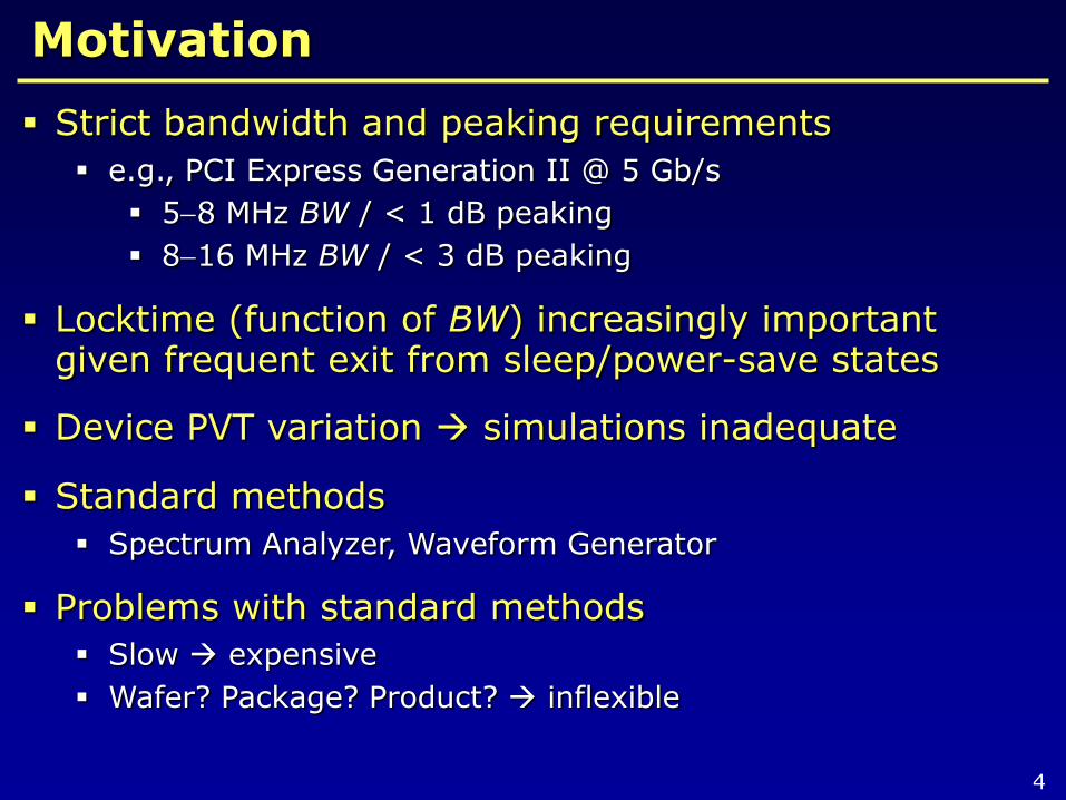
Motivation
Strict bandwidth and peaking requirements
e.g., PCI Express Generation II @ 5 Gb/s
58 MHz BW / < 1 dB peaking
816 MHz BW / < 3 dB peaking
Locktime (function of BW) increasingly important given frequent exit from sleep/power-save states
Device PVT variation simulations inadequate
Standard methods
Spectrum Analyzer, Waveform Generator
Problems with standard methods
Slow expensive
Wafer? Package? Product? inflexible
5
Outline
Motivation
Loop Measurement Circuit
• Algorithm
• Architecture
Silicon Results
Conclusion

6
Simulated Step Response vs. Time
0
+2
+4
+6
-6
-4
-2
-8
Time (µs)
Ph
ase
Err
or
(ns)
0.0 0.5 1.0 1.5 2.0 2.5 3.0 3.5 4.0
Tcrossover
MaxOvershoot
7
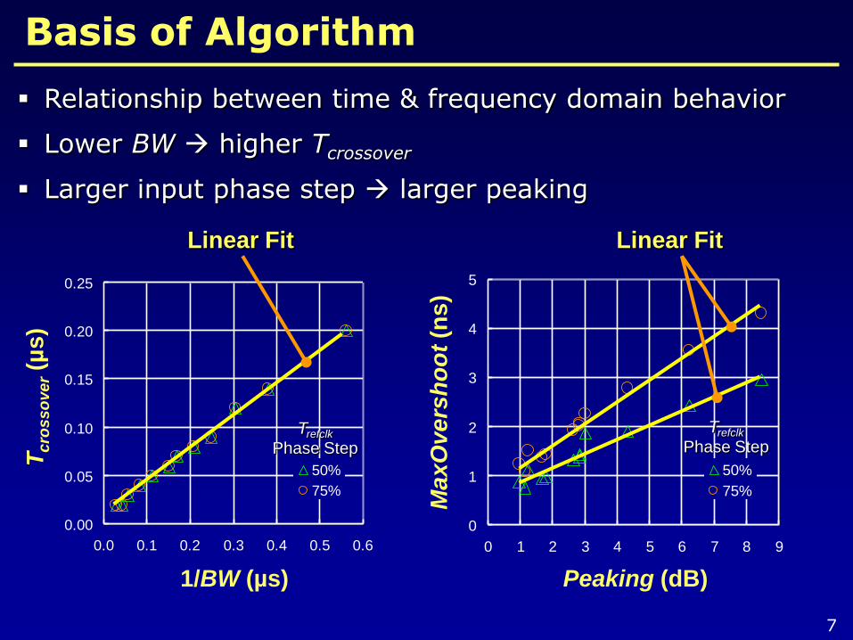
Basis of Algorithm
Relationship between time & frequency domain behavior
Lower BW higher Tcrossover
Larger input phase step larger peaking
0.00
0.05
0.10
0.15
0.20
0.25
0.0 0.1 0.2 0.3 0.4 0.5 0.6
50%
75%
1/BW (µs)
Tc
ros
so
ve
r(µ
s)
Linear Fit
Trefclk
Phase StepM
axO
vers
ho
ot
(ns)
Peaking (dB)
0
1
2
3
4
5
0 1 2 3 4 5 6 7 8 9
50%
75%
Trefclk
Phase Step
Linear Fit
8
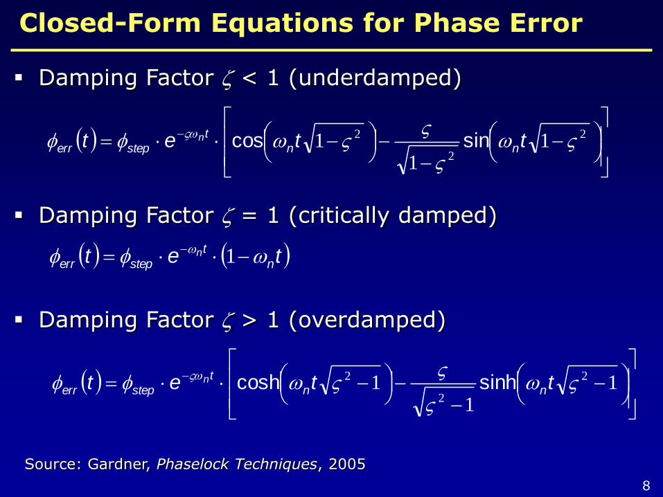
Closed-Form Equations for Phase Error
Damping Factor < 1 (underdamped)
Damping Factor = 1 (critically damped)
Damping Factor > 1 (overdamped)
tet n
t
steperrn
1
1
11 2
2
2
ttet nn
t
steperrn sinhcosh
2
2
2 11
1
ttet nn
t
steperrn sincos
Source: Gardner, Phaselock Techniques, 2005

9
Closed-Form Equations vs. Simulations
0.00
0.05
0.10
0.15
0.20
0.25
0.0 0.1 0.2 0.3 0.4 0.5 0.6
Simulation
Equation
1/BW (µs)
Tcro
sso
ve
r(µ
s)
Ma
xO
ve
rsh
oo
t (n
s)
Peaking (dB)
0
1
2
3
4
5
0 1 2 3 4 5 6 7 8 9
Simulation
Equation
75% Trefclk Phase Step 75% Trefclk Phase Step
Equations become less accurate at high due to smoothing loop filter pole for reference spur reduction
10
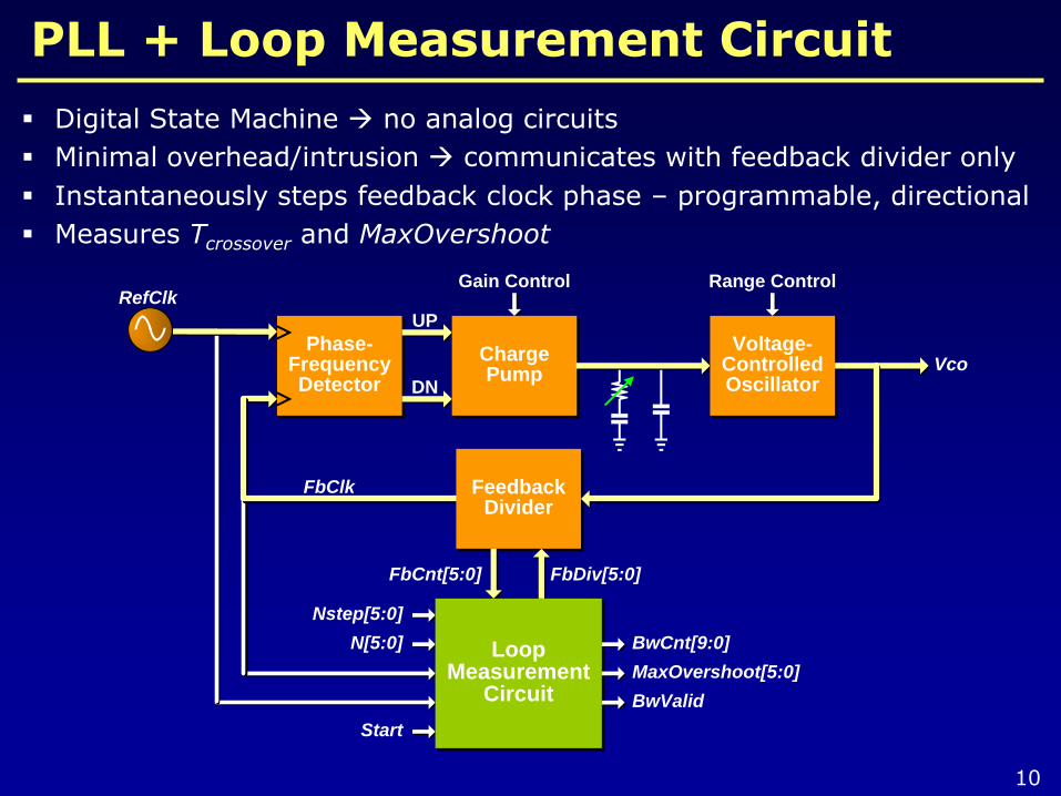
PLL + Loop Measurement Circuit
Digital State Machine no analog circuits
Minimal overhead/intrusion communicates with feedback divider only
Instantaneously steps feedback clock phase – programmable, directional
Measures Tcrossover and MaxOvershoot
UP
Gain Control Range ControlRefClk
FbClk
FbDiv[5:0]FbCnt[5:0]
Nstep[5:0]
N[5:0]
Start
BwCnt[9:0]
MaxOvershoot[5:0]
BwValid
FeedbackDivider
LoopMeasurement
Circuit
Phase-FrequencyDetector DN
ChargePump
Voltage-ControlledOscillator
Vco

11
Loop Measurement Circuit
DD QQ DD QQ
RefRiseRefRise
RefFallRefFallVcoVco VcoVco
RefClkRefClk
DD QQ DD QQ
StartRiseStartRise
VcoVco VcoVco
StartStart
FbDiv[5:0]FbDiv[5:0]
To Feedback
Divider
To Feedback
Divider
BwValidBwValid
BwEnBwEn
RefRiseRefRise
Edge DetectorEdge Detector
Edge DetectorEdge Detector
From
JTAG
From
JTAG
Control
Unit
Control
Unit
N[5:0]N[5:0]
N[5:0]+K[5:0]N[5:0]+K[5:0]
StepEnStepEn
DD QQ
RefClkRefClk
FbClkFbClkBBPDBBPD
DD QQ
VcoVco
BwValidBwValid
Tcrossover
Detector
Tcrossover
Detector
To JTAGTo JTAG
RefRiseRefRise
BBPD2BBPD2
Load_BBPDLoad_BBPD
CompareCompare
FbCnt[5:0]FbCnt[5:0]
RefRiseRefRise
VcoVco
DD QQ
SmplCnt[5:0]SmplCnt[5:0]
UpdateOSUpdateOS
RefFallRefFall
MaxOvershoot[5:0]MaxOvershoot[5:0]
NewMaxOSNewMaxOSMaxOvershoot
Detector
MaxOvershoot
Detector
From
Feedback
Divider
From
Feedback
Divider
VcoVco
FbRiseFbRise
VcoVco
ClrClr
DD QQ DD QQ
EnEn BBPD1BBPD1DD QQ
VcoVco
EnEn
VcoVco
EnEn
CounterCounterBWBW BwCnt[9:0]BwCnt[9:0]QQ
To JTAGTo JTAG
DD QQEnEn
Hold D
until
En=1
Hold D
until
En=1
EnEn EnEn
Delay D
until En=1
Hold D
until Clr=1
Delay D
until En=1
Hold D
until Clr=1

12
Control Unit
VcoVco
RefClkRefClk
RefFallRefFall
RefRiseRefRise
StartStart
StartRiseStartRise
StepEnStepEn
FbRiseFbRise
BwEnBwEn
DD QQ DD QQ
RefRiseRefRise
RefFallRefFallVcoVco VcoVco
RefClkRefClk
DD QQ DD QQ
StartRiseStartRise
VcoVco VcoVco
StartStart
FbDiv[5:0]FbDiv[5:0]
To Feedback
Divider
To Feedback
Divider
BwValidBwValid RefRiseRefRise
Edge DetectorEdge Detector
Edge DetectorEdge Detector
From
JTAG
From
JTAG
N[5:0]N[5:0]
N[5:0]+K[5:0]N[5:0]+K[5:0]
StepEnStepEn
VcoVco
FbRiseFbRise
VcoVco
ClrClr
DD QQ DD QQ
Hold D
until
En=1
Hold D
until
En=1
EnEn EnEn
Delay D
until En=1
Hold D
until Clr=1
Delay D
until En=1
Hold D
until Clr=1
To Tcrossover DetectorTo Tcrossover Detector
BwEnBwEn

13
Control Unit and Phase Step
VcoVco
RefClkRefClk
BwEnBwEn
BwCnt[9:0]BwCnt[9:0] 11 22 33 5544 66 77 88 99 1010 1111 1212 131300
FbDiv[5:0]FbDiv[5:0] 88 881111
FbClkFbClk
FbCnt[5:0]FbCnt[5:0] 1100 22 33 44 55 66 77 00 11 22 33 44 55 66 77 88 99 1010 1100 22 33 44 55 66 77 0077
StepEnStepEn
DD QQ DD QQ
RefRiseRefRise
RefFallRefFallVcoVco VcoVco
RefClkRefClk
DD QQ DD QQ
StartRiseStartRise
VcoVco VcoVco
StartStart
FbDiv[5:0]FbDiv[5:0]
To Feedback
Divider
To Feedback
Divider
BwValidBwValid RefRiseRefRise
Edge DetectorEdge Detector
Edge DetectorEdge Detector
From
JTAG
From
JTAG
N[5:0]N[5:0]
N[5:0]+K[5:0]N[5:0]+K[5:0]
StepEnStepEn
VcoVco
FbRiseFbRise
VcoVco
ClrClr
DD QQ DD QQ
Hold D
until
En=1
Hold D
until
En=1
EnEn EnEn
Delay D
until En=1
Hold D
until Clr=1
Delay D
until En=1
Hold D
until Clr=1
To Tcrossover DetectorTo Tcrossover Detector
BwEnBwEn

14
Bandwidth/Tcrossover Test
BwEnBwEn
DD QQ
RefClkRefClk
FbClkFbClkBBPDBBPD
DD QQ
VcoVco
BwValidBwValid
To JTAGTo JTAG
RefRiseRefRise
BBPD2BBPD2
Load_BBPDLoad_BBPD
EnEn BBPD1BBPD1DD QQ
VcoVco
EnEn
VcoVco
EnEn
CounterCounterBWBW BwCnt[9:0]BwCnt[9:0]QQ
From Control UnitFrom Control Unit
RefClkRefClk
BwCnt[5:0]BwCnt[5:0]
Load_BBPDLoad_BBPD
FbClkFbClk
BBPDBBPD
BBPD1BBPD1
BBPD2BBPD2
BwValidBwValid
VcoVco
4646 4747 4848 4949 5050 5151 5252 5353 5454 5555 5656 5757 5858 5959 60604444 4545

15
Peaking/MaxOvershoot Test
RefClkRefClk
FbCnt[5:0]FbCnt[5:0] 11 22 33 44 55 66 77 00 11 22 33 44 55 66 77 00 11 22 33 44 55 66 77 00 11 22 33 44
33 4422 33 22SmplCnt[5:0]SmplCnt[5:0]
RefFallRefFall
RefRiseRefRise
VcoVco
UpdateOSUpdateOS
4400MaxOvershoot[5:0]MaxOvershoot[5:0] 33
CompareCompare
FbCnt[5:0]FbCnt[5:0]
RefRiseRefRise
VcoVco
DD QQ
SmplCnt[5:0]SmplCnt[5:0]
UpdateOSUpdateOS
RefFallRefFall
MaxOvershoot[5:0]MaxOvershoot[5:0]
NewMaxOSNewMaxOS
From
Feedback
Divider
From
Feedback
DividerTo JTAGTo JTAG
DD QQEnEn
BwValidBwValid

16
Outline
Motivation
Loop Measurement Circuit
• Algorithm
• Architecture
Silicon Results
Conclusion

17
Simulations vs. Measurements
100 MHz refclk, feedback divisor = 50 (2x25)
CaseRlpf
(kW)
Icp
(µA)
Bandwidth (MHz) Peaking (dB)
Simulated
Measured
Simulated
Measured
Part
1
Part
2
Part
3
Part
1
Part
2
Part
3
1 3.2 2.5 1.8 3.4 3.4 3.0 8.5 4.2 4.1 4.2
2 3.2 5 2.6 3.1 3.2 3.2 6.2 4.3 4.0 4.2
3 3.2 10 4.0 5.0 5.4 5.3 4.3 3.0 2.8 2.8
4 3.2 20 6.6 9.3 10.0 10.0 2.9 1.8 1.5 1.7
5 4.8 10 4.8 6.2 6.8 6.5 2.6 1.7 1.5 1.3
6 4.8 20 9.0 13.2 14.8 14.2 1.7 0.9 0.7 0.7
7 6.4 5 3.3 4.3 4.5 4.5 2.8 1.9 2.0 1.7
8 6.4 10 6.0 8.1 9.1 9.0 1.8 1.1 1.0 1.0
9 6.4 20 12.0 17.6 19.7 18.7 1.2 0.7 1.1 1.0
10 6.4 30 18.1 25.6 27.1 26.2 0.8 2.1 2.6 2.8
11 6.4 40 23.3 25.7 26.8 26.1 1.2 2.2 2.5 2.8
12 6.4 70 35.2 25.7 26.7 25.9 3.0 2.1 2.3 2.6
18
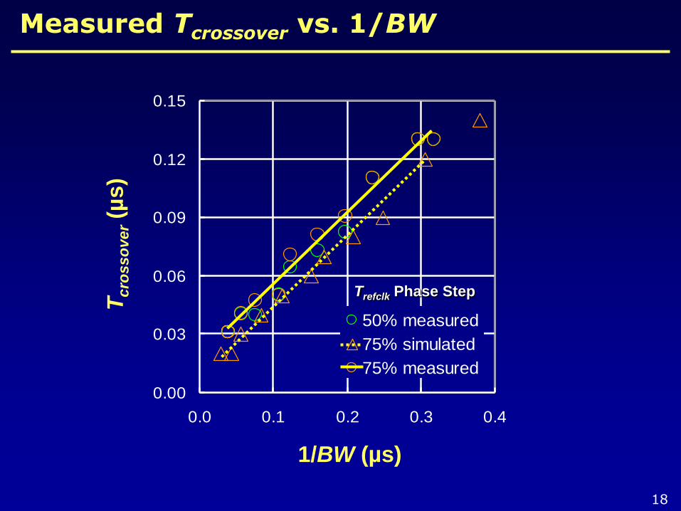
Measured Tcrossover vs. 1/BW
1/BW (µs)
Tcro
sso
ver(µ
s)
0.00
0.03
0.06
0.09
0.12
0.15
0.0 0.1 0.2 0.3 0.4
50% measured
75% simulated
75% measured
Trefclk Phase Step

19
Measured MaxOvershoot vs. Peaking
Ma
xO
ve
rsh
oo
t (n
s)
Peaking (dB)
0.0
0.5
1.0
1.5
2.0
2.5
3.0
0 1 2 3 4 5
50% simulated
50% measured
75% simulated
75% measured
Trefclk Phase Step
20
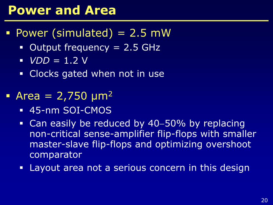
Power and Area
Power (simulated) = 2.5 mW
Output frequency = 2.5 GHz
VDD = 1.2 V
Clocks gated when not in use
Area = 2,750 µm2
45-nm SOI-CMOS
Can easily be reduced by 4050% by replacing non-critical sense-amplifier flip-flops with smaller master-slave flip-flops and optimizing overshoot comparator
Layout area not a serious concern in this design

21
Outline
Motivation
Loop Measurement Circuit
• Algorithm
• Architecture
Silicon Results
Conclusions

22
Conclusion
An on-chip, all-digital state machine can be used to accurately estimate PLL bandwidth and peaking with potentially large savings in tester time.
This flexible circuit may be used from wafer level to product level, minimizing die/package waste and allowing for adaptive PLL loop calibration.

23
Acknowledgments
Alvin Loke - AMD
Gerry Talbot - AMD