4-channel, i c, ultra low power, 12-bit adc in 20 … instruments mobile communications...
TRANSCRIPT

4-Channel, I2C, Ultra Low Power, 12-Bit ADC in 20-Lead LFCSP/TSSOP
Data Sheet AD7091R-5
Rev. A Document Feedback Information furnished by Analog Devices is believed to be accurate and reliable. However, no responsibility is assumed by Analog Devices for its use, nor for any infringements of patents or other rights of third parties that may result from its use. Specifications subject to change without notice. No license is granted by implication or otherwise under any patent or patent rights of Analog Devices. Trademarks and registered trademarks are the property of their respective owners.
One Technology Way, P.O. Box 9106, Norwood, MA 02062-9106, U.S.A. Tel: 781.329.4700 ©2015–2018 Analog Devices, Inc. All rights reserved. Technical Support www.analog.com
FEATURES I2C-compatible serial interface supports standard and
fast modes Ultra low power: 90 µW typical at 3 V in fast mode Specified for VDD of 2.7 V to 5.25 V On-chip accurate 2.5 V reference, 5 ppm/°C typical drift 4 single-ended analog input channels ALERT function BUSY function Autocycle mode Wide input bandwidth
68 dB signal-to-noise ratio (SNR) typical at input frequency of 1 kHz
Flexible power/throughput rate management No pipeline delays Power-down mode
550 nA typical at VDD = 5.25 V 435 nA typical at VDD = 3 V
20-lead LFCSP and TSSOP packages Temperature range: −40°C to +125°C
APPLICATIONS Battery-powered systems
Personal digital assistants Medical instruments Mobile communications
Instrumentation and control systems Data acquisition systems Optical sensors Diagnostic/monitoring functions
FUNCTIONAL BLOCK DIAGRAM
INPUTMUX
CHANNELSEQUENCER CONTROL
LOGICI2C INTERFACE
T/H
RESETCONVST/GPO1SDASCLAS0AS1VDRIVE
VIN0
MUXOUT ADCIN VDDREFIN/
REFOUT REGCAP
ALERT/BUSY/GPO0
GPO2 GNDGND
VIN1
VIN2
VIN3
12-BITSUCCESSIVE
APPROXIMATIONADC
ON-CHIPOSC
2.5VVREF
AD7091R-5
1209
3-00
1
Figure 1.
GENERAL DESCRIPTION The AD7091R-5 is a 12-bit, multichannel, ultra low power, succes-sive approximation analog-to-digital converter (ADC). The AD7091R-5 operates from a single 2.7 V to 5.25 V power supply and typically consumes only 24 µA at a 3 V supply in fast mode.
The AD7091R-5 provides a 2-wire serial interface compatible with I2C interfaces. The conversion process can be controlled by a sample mode via the CONVST/GPO1 pin, an autocycle mode selected through software control, or a command mode in which conversions occur across I2C write operations.
The device contains a wide bandwidth track-and-hold amplifier that can handle input frequencies up to 1.5 MHz. The AD7091R-5 also features an on-chip conversion clock, an on-chip accurate 2.5 V reference, and a programmable out of bounds user alert function.
The AD7091R-5 offers four single-ended analog input channels with a channel sequencer that allows a preprogrammed selection of channels to be converted sequentially.
The AD7091R-5 uses advanced design techniques to achieve ultra low power dissipation without compromising performance. It also features flexible power management options. An on-chip configuration register allows the user to set up different operating conditions. These include power management, alert functionality, busy indication, channel sequencing, and general-purpose output pins. The MUXOUT and ADCIN pins allow signal conditioning of the multiplexer output before acquisition by the ADC.

AD7091R-5 Data Sheet
Rev. A | Page 2 of 34
TABLE OF CONTENTS Features .............................................................................................. 1 Applications ....................................................................................... 1 Functional Block Diagram .............................................................. 1 General Description ......................................................................... 1 Revision History ............................................................................... 2 Specifications ..................................................................................... 3
I2C Timing Specifications ............................................................ 5 Absolute Maximum Ratings ............................................................ 6
Thermal Resistance ...................................................................... 6 ESD Caution .................................................................................. 6
Pin Configurations and Function Descriptions ........................... 7 Typical Performance Characteristics ............................................. 9 Terminology .................................................................................... 14 Theory of Operation ...................................................................... 15
Circuit Information .................................................................... 15 Converter Operation .................................................................. 15 ADC Transfer Function ............................................................. 15 Reference ..................................................................................... 15 Power Supply ............................................................................... 16 Device Reset ................................................................................ 16 Analog Input ............................................................................... 16 Driver Amplifier Choice ............................................................ 17 Typical Connection Diagram ................................................... 17
I2C Registers .................................................................................... 19 Addressing Registers .................................................................. 19 Slave Address ............................................................................... 19
I2C Register Access ..................................................................... 19 Conversion Result Register ....................................................... 20 Channel Register ........................................................................ 21 Configuration Register .............................................................. 22 Alert Indication Register ........................................................... 24 Channel x Low Limit Register .................................................. 26 Channel x High Limit Register ................................................. 26 Channel x Hysteresis Register .................................................. 26
I2C Interface .................................................................................... 27 Serial Bus Address Byte ............................................................. 27 General I2C Timing .................................................................... 27
Writing to the AD7091R-5 ............................................................ 28 Writing Two Bytes of Data to a 16-Bit Register ..................... 28 Writing to Multiple Registers .................................................... 28
Reading Data from the AD7091R-5 ............................................. 29 Reading Two Bytes of Data from a 16-Bit Register ............... 29
Modes of Operation ....................................................................... 30 Sample Mode .............................................................................. 30 Command Mode ........................................................................ 30 Autocycle Mode .......................................................................... 32 Power-Down Mode .................................................................... 32 Alert ............................................................................................. 33 Busy .............................................................................................. 33 Channel Sequencer .................................................................... 33
Outline Dimensions ....................................................................... 34 Ordering Guide .......................................................................... 34
REVISION HISTORY 2/2018—Rev. 0 to Rev. A Changes to Command Mode Section and Figure 43 ................. 31 Updated Outline Dimensions ....................................................... 34 Changes to Ordering Guide .......................................................... 34 7/2015—Revision 0: Initial Version

Data Sheet AD7091R-5
Rev. A | Page 3 of 34
SPECIFICATIONS VDD = 2.7 V to 5.25 V, VDRIVE = 1.8 V to 5.25 V, fSCL = 400 kHz, fast SCL mode, VREF = 2.5 V internal/external, TA = −40°C to +125°C, unless otherwise noted.
Table 1. Parameter Test Conditions/Comments Min Typ Max Unit DYNAMIC PERFORMANCE fIN = 1 kHz sine wave
Signal-to-Noise Ratio (SNR) 68 dB Signal-to-Noise-and-Distortion Ratio
(SINAD) 67 dB
Total Harmonic Distortion (THD) −80 dB Spurious-Free Dynamic Range (SFDR) −81 dB Channel to Channel Isolation −105 dB Aperture Delay 5 ns Aperture Jitter 40 ps Full Power Bandwidth At −3 dB 1.5 MHz At −0.1 dB 1.2 MHz
DC ACCURACY Resolution 12 Bits Integral Nonlinearity (INL) −1.25 ±0.8 +1.25 LSB Differential Nonlinearity (DNL) Guaranteed no missing codes to 12 bits −0.9 ±0.3 +0.9 LSB Offset Error TA = 25°C −1.5 ±0.3 +1.5 mV Offset Error Matching TA = 25°C −1.5 ±0.3 +1.5 mV Offset Error Drift 2 ppm/°C Gain Error TA = 25°C −0.1 0.0 +0.1 % FS Gain Error Matching TA = 25°C −0.1 0.0 +0.1 % FS Gain Error Drift 1 ppm/°C
ANALOG INPUT Input Voltage Range1 At ADCIN 0 VREF V DC Leakage Current −1 +1 µA Input Capacitance2 During acquisition phase 10 pF Outside acquisition phase 1.5 pF Multiplexer On Resistance VDD = 5.0 V 50 Ω VDD = 2.5 V 100 Ω
VOLTAGE REFERENCE INPUT/OUTPUT REFOUT
3 Internal reference output, TA = 25°C 2.49 2.5 2.51 V REFIN
3 External reference input 1.0 VDD V Drift 5 ppm/°C Power-On Time CREF = 2.2 µF 50 ms
LOGIC INPUTS Input Voltage
High (VIH) 0.7 × VDRIVE V Low (VIL) 0.3 × VDRIVE V
Input Current (IIN) VIN = 0 V or VDRIVE −1 0.01 +1 µA LOGIC OUTPUTS
Output Voltage High (VOH) ISOURCE = 200 µA VDRIVE − 0.2 V Low (VOL) ISINK = 200 µA 0.4 V
Floating State Leakage Current −1 +1 µA Output Coding Straight (natural) binary

AD7091R-5 Data Sheet
Rev. A | Page 4 of 34
Parameter Test Conditions/Comments Min Typ Max Unit CONVERSION RATE
Conversion Time 550 ns Update Rate
Autocycle Setting 00 90 100 110 μs Autocycle Setting 01 180 200 220 μs Autocycle Setting 10 360 400 440 μs Autocycle Setting 11 720 800 880 μs
Throughput Rate fSCL = 400 kHz, command mode 22.22 kSPS POWER REQUIREMENTS
VDD 2.7 5.25 V VDRIVE Range 1.8 5.25 V IDD VIN = 0 V
Normal Mode—Static VDD = 5.25 V 22 50 µA VDD = 3 V 21.6 46 µA Normal Mode—Operational VDD = 5.25 V, fSCL = 400 kHz 26 55 µA VDD = 3 V, fSCL = 400 kHz 24 52 µA VDD = 5.25 V, fSCL = 100 kHz 25 54 µA VDD = 3 V, fSCL = 100 kHz 23 51 µA VDD = 3 V, autocycle mode 70 105 µA Power-Down Mode VDD = 5.25 V 0.550 17 µA VDD = 5.25 V, TA = −40°C to +85°C 0.550 8 µA VDD = 3 V 0.435 15 µA
IDRIVE VIN = 0 V Normal Mode—Static VDRIVE = 5.25 V 2 4 µA VDRIVE = 3 V 1 3.5 µA Normal Mode—Operational VDRIVE = 5.25 V, fSCL = 400 kHz 6 15 µA VDRIVE = 3 V, fSCL = 400 kHz 5 14 µA VDRIVE = 5.25 V, fSCL = 100 kHz 5 14 µA VDRIVE = 3 V, fSCL = 100 kHz 4 13 µA
Total Power Dissipation4 VIN = 0 V Normal Mode—Static VDD = VDRIVE = 5.25 V 130 290 µW VDD = VDRIVE = 3 V 70 150 µW Normal Mode—Operational VDD = VDRIVE = 5.25 V, fSCL = 400 kHz 170 370 µW VDD = VDRIVE = 3 V, fSCL = 400 kHz 90 200 µW VDD = VDRIVE = 5.25 V, fSCL = 100 kHz 160 360 µW VDD = VDRIVE = 3 V, fSCL = 100 kHz 85 195 µW VDD = VDRIVE = 3 V, autocycle mode 210 315 µW Power-Down Mode VDD = 5.25 V 3 95 µW VDD = 5.25 V, TA = −40°C to +85°C 3 33 µW VDD = VDRIVE = 3 V 1.4 50 µW
1 The multiplexer input voltage must not exceed VDD. 2 Sample tested during initial release to ensure compliance. 3 When referring to a single function of a multifunction pin in the parameters, only the portion of the pin name that is relevant to the specification is listed. For full pin
names of multifunction pins, see the Pin Configurations and Function Descriptions section. 4 Total power dissipation includes contributions from VDD, VDRIVE, and REFIN (see Note 3).
Data Sheet AD7091R-5
Rev. A | Page 5 of 34
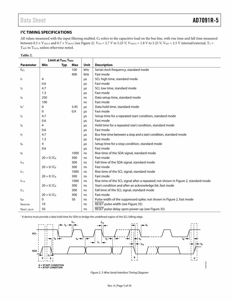
I2C TIMING SPECIFICATIONS All values measured with the input filtering enabled. CB refers to the capacitive load on the bus line, with rise time and fall time measured between 0.3 × VDRIVE and 0.7 × VDRIVE (see Figure 2). VDD = 2.7 V to 5.25 V, VDRIVE = 1.8 V to 5.25 V, VREF = 2.5 V internal/external, TA = TMIN to TMAX, unless otherwise noted.
Table 2. Limit at TMIN, TMAX Parameter Min Typ Max Unit Description fSCL
100 kHz Serial clock frequency, standard mode 400 kHz Fast mode t1
4 µs SCL high time, standard mode 0.6 µs Fast mode t2
4.7 µs SCL low time, standard mode 1.3 µs Fast mode t3
250 ns Data setup time, standard mode 100 ns Fast mode t4
1 0 3.45 µs Data hold time, standard mode 0 0.9 µs Fast mode t5
4.7 µs Setup time for a repeated start condition, standard mode 0.6 µs Fast mode t6
4 µs Hold time for a repeated start condition, standard mode 0.6 µs Fast mode t7
4.7 µs Bus-free time between a stop and a start condition, standard mode 1.3 µs Fast mode t8
4 µs Setup time for a stop condition, standard mode 0.6 µs Fast mode t9 1000 ns Rise time of the SDA signal, standard mode 20 + 0.1CB 300 ns Fast mode t10 300 ns Fall time of the SDA signal, standard mode 20 + 0.1CB 300 ns Fast mode t11 1000 ns Rise time of the SCL signal, standard mode 20 + 0.1CB 300 ns Fast mode t11A 1000 ns Rise time of the SCL signal after a repeated; not shown in Figure 2, standard mode 20 + 0.1CB 300 ns Start condition and after an acknowledge bit, fast mode t12 300 ns Fall time of the SCL signal, standard mode 20 + 0.1CB 300 ns Fast mode tSP
0 50 ns Pulse width of the suppressed spike; not shown in Figure 2, fast mode tRESETPW 10 ns RESET pulse width (see Figure 35)
tRESET_DELAY 50 ns RESET pulse delay upon power-up (see Figure 35) 1 A device must provide a data hold time for SDA to bridge the undefined region of the SCL falling edge.
t6
t7
t2
t11
t4t1
t12
t10
t5
t9
t6
t3 t8
SCL
S
SDA
S = START CONDITIONP = STOP CONDITION
P PS
1209
3-00
2
Figure 2. 2-Wire Serial Interface Timing Diagram

AD7091R-5 Data Sheet
Rev. A | Page 6 of 34
ABSOLUTE MAXIMUM RATINGS TA = 25°C, unless otherwise noted.
Table 3. Parameter Rating VDD to GND −0.3 V to +7 V VDRIVE to GND −0.3 V to +7 V Analog Input Voltage to GND −0.3 V to VREF + 0.3 V Digital Input1 Voltage to GND −0.3 V to VDRIVE + 0.3 V Digital Output2 Voltage to GND −0.3 V to VDRIVE + 0.3 V Input Current to Any Pin Except
Supplies3 ±10 mA Operating Temperature Range −40°C to +125°C Storage Temperature Range −65°C to +150°C Junction Temperature 150°C ESD
Human Body Model (HBM) 1.5 kV Field Induced Charged Device
Model (FICDM) 500 V
1 The digital input pins include the following: AS0, RESET, AS1, SCL, SDA,
and CONVST/GPO1. 2 The digital output pins include: ALERT/BUSY/GPO0, GPO2, and SDA. 3 Transient currents of up to 100 mA do not cause SCR latch-up.
Stresses at or above those listed under Absolute Maximum Ratings may cause permanent damage to the product. This is a stress rating only; functional operation of the product at these or any other conditions above those indicated in the operational section of this specification is not implied. Operation beyond the maximum operating conditions for extended periods may affect product reliability.
THERMAL RESISTANCE θJA is specified for the worst case conditions, that is, a device soldered in a circuit board for surface-mount packages.
Table 4. Thermal Resistance Package Type θJA θJC Unit 20-Lead LFCSP_WQ 52 6.5 °C/W 20-Lead TSSOP 84.3 18.4 °C/W
ESD CAUTION

Data Sheet AD7091R-5
Rev. A | Page 7 of 34
PIN CONFIGURATIONS AND FUNCTION DESCRIPTIONS
AD7091R-5TOP VIEW
(Not to Scale)
1
2
3
4
5
6
7
8
9
10
RESET
VDD
REGCAP
MUXOUT
GND
REFIN/REFOUT
AS0
ALERT/BUSY/GPO0
VIN2
VIN0
20
19
18
17
16
15
14
13
12
11
CONVST/GPO1
SCL
SDA
ADCIN
GND
AS1
GPO2
VIN3
VIN1
VDRIVE
1209
3-00
4
Figure 3. Pin Configuration, 20-Lead TSSOP
NOTES1. EXPOSED PAD. THE EXPOSED PAD IS NOT CONNECTED
INTERNALLY. IT IS RECOMMENDED THAT THE PAD BESOLDERED TO GND.
14
13
12
1
3
4
AS1
15 SDA
GNDADCIN
11 VIN1
VDD
REFIN/REFOUT
2REGCAP
GND
5MUXOUT
7V I
N2
6V I
N0
8A
LER
T/B
USY
/GPO
0
9G
PO2
10V I
N3
19A
S 0
20R
ESET
18V D
RIV
E
17C
ON
VST/
GPO
1
16SC
L
AD7091R-5TOP VIEW
(Not to Scale)
1209
3-00
3
Figure 4. Pin Configuration, 20-Lead LFCSP
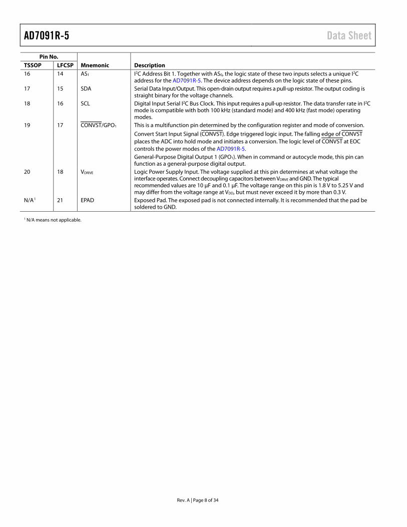
Table 5. Pin Function Descriptions Pin No.
Mnemonic Description TSSOP LFCSP 1 19 AS0 I2C Address Bit 0. Together with AS1, the logic state of these two inputs selects a unique I2C
address for the AD7091R-5. The device address depends on the logic state of these pins. 2 20 RESET Reset. Logic input. This pin resets the device when pulled low.
3 1 VDD Power Supply Input. The VDD range is from 2.7 V to 5.25 V. Decouple this supply pin to GND. 4 2 REGCAP Decoupling Capacitor Pin for Voltage Output from the Internal Regulator. Decouple this output
pin separately to GND using a 2.2 µF capacitor. 5 3 REFIN/REFOUT Voltage Reference Output, 2.5 V. Decouple this pin to GND. The typical recommended
decoupling capacitor value is 2.2 µF. The user can either access the internal 2.5 V reference or overdrive the internal reference with the voltage applied to this pin. The reference voltage range for an externally applied reference is 1.0 V to VDD.
6, 15 4, 13 GND Chip Ground Pins. These pins are the ground reference point for all circuitry on the AD7091R-5. 7 5 MUXOUT Multiplexer Output. The output of the multiplexer appears at this pin. If no external filtering or
buffering is required, tie this pin directly to the ADCIN pin; otherwise, tie the output of the conditioning network to the ADCIN pin.
8 6 VIN0 Analog Input for Channel 0. Single-ended analog input. The analog input range is 0 V to VREF. 9 7 VIN2 Analog Input for Channel 2. Single-ended analog input. The analog input range is 0 V to VREF. 10 8 ALERT/BUSY/GPO0 This is a multifunction pin determined by the configuration register. Alert Output Pin (ALERT). When functioning as ALERT, this pin is a logic output indicating that a
conversion result has fallen outside the limit of the register settings. Busy Output (BUSY). The BUSY pin indicates when a conversion is taking place. General-Purpose Digital Output 0 (GPO0). 11 9 GPO2 General-Purpose Digital Output 2. 12 10 VIN3 Analog Input for Channel 3. Single-ended analog input. The analog input range is 0 V to VREF. 13 11 VIN1 Analog Input for Channel 1. Single-ended analog input. The analog input range is 0 V to VREF. 14 12 ADCIN ADC Input. This pin allows direct access to the ADC. If no external filtering or buffering is
required, tie this pin directly to the MUXOUT pin; otherwise, tie the input of the conditioning network to the MUXOUT pin.
AD7091R-5 Data Sheet
Rev. A | Page 8 of 34
Pin No. Mnemonic Description TSSOP LFCSP
16 14 AS1 I2C Address Bit 1. Together with AS0, the logic state of these two inputs selects a unique I2C address for the AD7091R-5. The device address depends on the logic state of these pins.
17 15 SDA Serial Data Input/Output. This open-drain output requires a pull-up resistor. The output coding is straight binary for the voltage channels.
18 16 SCL Digital Input Serial I2C Bus Clock. This input requires a pull-up resistor. The data transfer rate in I2C mode is compatible with both 100 kHz (standard mode) and 400 kHz (fast mode) operating modes.
19 17 CONVST/GPO1 This is a multifunction pin determined by the configuration register and mode of conversion.
Convert Start Input Signal (CONVST). Edge triggered logic input. The falling edge of CONVSTplaces the ADC into hold mode and initiates a conversion. The logic level of CONVST at EOC controls the power modes of the AD7091R-5.
General-Purpose Digital Output 1 (GPO1). When in command or autocycle mode, this pin can function as a general-purpose digital output.
20 18 VDRIVE Logic Power Supply Input. The voltage supplied at this pin determines at what voltage the interface operates. Connect decoupling capacitors between VDRIVE and GND. The typical recommended values are 10 µF and 0.1 µF. The voltage range on this pin is 1.8 V to 5.25 V and may differ from the voltage range at VDD, but must never exceed it by more than 0.3 V.
N/A1 21 EPAD Exposed Pad. The exposed pad is not connected internally. It is recommended that the pad be soldered to GND.
1 N/A means not applicable.

Data Sheet AD7091R-5
Rev. A | Page 9 of 34
TYPICAL PERFORMANCE CHARACTERISTICS 1.0
–1.0
–0.8
–0.6
–0.4
–0.2
0
0.2
0.4
0.6
0.8
INL
(LSB
)
CODE
VDD = 3.0VVREF = 2.5VfSCL = 400kHzTA = 25°CPOSITIVE INL = +0.43 LSBNEGATIVE INL = –0.66 LSB
0 512 1024 1536 2048 2560 3072 3584 4095
1209
3-20
5
Figure 5. INL vs. Code
1.0
–1.0
–0.8
–0.6
–0.4
–0.2
0
0.2
0.4
0.6
0.8
1.0 1.5 2.0 2.5 3.0 3.5 4.0 4.5 5.0 5.5
INL
(LSB
)
REFERENCE INPUT VOLTAGE (V)
MIN INL (LSB)
MAX INL (LSB)
VDD = 5.25VVREF = EXTERNALfSCL = 400kHzTA = 25°C
1209
3-23
1
Figure 6. Minimum/Maximum INL vs. External Reference Input Voltage
8000
7000
6000
5000
4000
3000
2000
1000
0
NU
MB
ER O
F O
CC
UR
REN
CES
CODE
VDD = VDRIVE = 3.3VVREF = 2.5V8192 SAMPLESTA = 25°C
290
7218
684
2028 2029 2030
1209
3-20
6
Figure 7. Histogram of a DC Input at Code Center
1.0
–1.0
–0.8
–0.6
–0.4
–0.2
0
0.2
0.4
0.6
0.8
DN
L (L
SB)
CODE
VDD = 3.0VVREF = 2.5VfSCL = 400kHzTA = 25°CPOSITIVE DNL = +0.41 LSBNEGATIVE DNL = –0.41 LSB
0 512 1024 1536 2048 2560 3072 3584 4095
1209
3-20
8
Figure 8. DNL vs. Code
1.0
–1.0
–0.8
–0.6
–0.4
–0.2
0
0.2
0.4
0.6
0.8
1.0 1.5 2.0 2.5 3.0 3.5 4.0 4.5 5.0 5.5
DN
L (L
SB)
REFERENCE INPUT VOLTAGE (V)
MIN DNL (LSB)
MAX DNL (LSB)
VDD = 5.25VVREF = EXTERNALfSCL = 400kHzTA = 25°C
1209
3-23
4
Figure 9. Minimum/Maximum DNL vs. External Reference Input Voltage
5000
4500
4000
3500
3000
2500
2000
1500
1000
500
0
NU
MB
ER O
F O
CC
UR
REN
CES
CODE
VDD = VDRIVE = 3.3VVREF = 2.5V8192 SAMPLESTA = 25°C
2042 2043 2044 2045
27
3762
4353
50
1209
3-20
9
Figure 10. Histogram of a DC Input at Code Transition

AD7091R-5 Data Sheet
Rev. A | Page 10 of 34
0
–160
–140
–120
–100
–80
–60
–40
–20
AD
C O
UTP
UT
SPEC
TRU
M (d
B)
FREQUENCY (Hz)0 100008000600040002000
VDD = VDRIVE = 3.3VVREF = 2.5V EXTERNALTA = 25°CfIN = 1kHzfSAMPLE = 22.2kSPSfSCL = 400kHzSNR = 68.3dBSINAD = 68.2dBTHD = –85.3dBSFDR = –88.2dB
1209
3-20
7
Figure 11. 10 kHz FFT, VDD = 3.0 V, VREF = 2.5 V External
0
–160
–140
–120
–100
–80
–60
–40
–20
AD
C O
UTP
UT
SPEC
TRU
M (d
B)
FREQUENCY (Hz)0 100008000600040002000
VDD = VDRIVE = 3.3VVREF = 2.5V INTERNALfIN = 1kHzfSAMPLE = 22.2kSPSfSCL = 400kHzSNR = 68.4dBSINAD = 68.2dBTHD = –83.3dBSFDR = –87.9dB
1209
3-21
0
Figure 12. 10 kHz FFT, VDD = 3.0 V, VREF = 2.5 V Internal
64
65
66
67
68
69
70
1 10 100
SNR,
SIN
AD (d
B)
INPUT FREQUENCY (kHz) 1209
3-10
8
VDD = 3.3VVREF = 2.5VSIGNAL AMPLITUDE = –0.5dBfSCL = 400kHzTA = 25°C
SNRSINAD
Figure 13. SNR, SINAD vs. Input Frequency
66
SNR
, SIN
AD
(dB
)
REFERENCE INPUT VOLTAGE (V)1.0
71
70
1.5
65
64
63
62
67
69
2.5 4.0 4.5 5.0
11.7
11.5
11.3
11.1
10.9
10.7
10.5
10.3
10.1
9.9
ENO
B (B
its)
2.0 3.0 3.5
68
ENOBSINADSNR
VDD = 3.0VVREF = EXTERNALfSCL = 400kHzfIN = 1kHzSIGNAL AMPLITUDE = –0.5dBTA = 25°C
1209
3-21
3
Figure 14. SNR, SINAD, and ENOB vs. Reference Input Voltage
–90
–88
–86
–84
–82
–80
–78
–76
–74
–72
–70
1 10 100
THD
(dB
)
ANALOG INPUT FREQUENCY (kHz) 1209
3-10
9
VDD = 3.3VVREF = 2.5VSIGNAL AMPLITUDE = –0.5dBfSCL = 400kHzTA = 25°C
Figure 15. THD vs. Analog Input Frequency
70.0
69.5
69.0
68.5
68.0
67.5
67.0
66.5
66.0
SNR
(dB
)
INPUT LEVEL (dB)
VDD = 3.0VVREF = 2.5VfSCL = 400kHzfIN = 1kHzTA = 25°C
–10 0–1–2–3–4–5–6–7–8–9
1209
3-21
5
Figure 16. SNR vs. Input Level
Data Sheet AD7091R-5
Rev. A | Page 11 of 34
THD
, SFD
R (d
B)
REFERENCE INPUT VOLTAGE (V)1.0
–75
1.5–95
–93
–91
–89
–87
–85
–83
–81
–79
–77
2.5 4.0 4.5 5.02.0 3.0 3.5
SFDRTHD VDD = 3.0V
VREF = EXTERNALfSCL = 400kHzfIN = 1kHzSIGNAL AMPLITUDE = –0.5dBTA = 25°C
1209
3-21
6
Figure 17. THD, SFDR vs. Reference Input Voltage
–81
–85
–90–55
THD
(dB
)
TEMPERATURE (°C)–35 –15 5 25 45
–80
65 85
–82
–83
–84
–86
–87
–88
–89
105 125
VDD = 5.0VfSCL = 400kHzfIN = 1kHz
1209
3-12
9
Figure 18. THD vs. Temperature
68.6
–55
SNR
(dB
)
TEMPERATURE (°C)–35 –15 5 25 45
68.8
65 85
68.4
68.2
68.0
67.6
67.4
67.2
67.0105 125
67.8
VDD = 3.0VVREF = 2.5VfSCL = 400kHzfIN = 1kHz
1209
3-12
2
Figure 19. SNR vs. Temperature
OPE
RA
TIO
NA
L I D
D S
UPP
LY C
UR
REN
T (µ
A)
TEMPERATURE (°C)–55
50
2510
15
20
25
30
35
40
45
12585
VDD = 3.0VVREF = INTERNAL 2.5VfSCL = 400kHz
2.70V3.00V5.25V
1209
3-22
0
Figure 20. Operational IDD Supply Current vs. Temperature
for Various VDD Supply Voltages
5
TOTA
L PO
WER
-DO
WN
CU
RR
ENT
(µA
)
TEMPERATURE (°C)–40
8
25
4
3
2
1
085 125
6
7
3.3V5.0V5.25V
2.7V
1209
3-12
7
Figure 21. Total Power-Down Current vs. Temperature for Various Supply Voltages
V REF
(V)
CURRENT LOAD (µA)0
2.510
2.505
2.500
2.495
2.490100908070605040302010
VDD = VDRIVE = 3.0V –55°C–40°C+25°C+85°C+125°C
1209
3-22
3
Figure 22. Reference Voltage Output (VREF) vs. Current Load
for Various Temperatures

AD7091R-5 Data Sheet
Rev. A | Page 12 of 34
OFF
SET
ERR
OR
(mV)
TEMPERATURE (°C)–55 –35 –15 5 25 45 65 85 105
1.5
–1.5
–1.0
–0.5
0
0.5
1.0
125
VDD = 3.0VVREF = 2.5VfSCL = 400kHz
1209
3-22
4
OFFSET ERROR CH 0OFFSET ERROR CH 1OFFSET ERROR CH 2OFFSET ERROR CH 3
Figure 23. Offset Error vs. Temperature
–1.5
–1.0
–0.5
0
0.5
1.0
–55
OFF
SET
ERR
OR
MA
TCH
(mV)
TEMPERATURE (°C)–35 –15 5 25 45
1.5
65 85 105 125
VDD = 3.0VVREF = 2.5VfSCL = 400kHz
1209
3-32
5
Figure 24. Offset Error Match vs. Temperature
75
80
85
90
95
100
1k
PSR
R (d
B)
RIPPLE FREQUENCY (Hz)
105
1M100k10k
VDD = 3.0VVREF = 2.5VfSCL = 400kHzTA = 25°C
1209
3-32
6
INTERNAL REFERENCE
EXTERNAL REFERENCE
Figure 25. PSRR vs. Ripple Frequency
GA
IN E
RR
OR
(% F
S)
TEMPERATURE (°C)–55 –35 –15 5 25 45 65 85 105
0.10
–0.10
–0.08
–0.06
–0.04
–0.02
0
0.02
0.04
0.06
0.08
125
VDD = 3.0VVREF = 2.5VfSCL = 400kHz
1209
3-22
7
GAIN ERROR CH 0GAIN ERROR CH 1GAIN ERROR CH 2GAIN ERROR CH 3
Figure 26. Gain Error vs. Temperature
0.08
0
–0.10–55
GA
IN E
RR
OR
MA
TCH
(% F
S)
TEMPERATURE (°C)–35 –15 5 25 45
0.10
65 85
0.06
0.04
0.02
–0.02
–0.04
–0.06
–0.08
105 125
VDD = 3.0VVREF = 2.5VfSCL = 400kHz
1209
3-32
8
Figure 27. Gain Error Match vs. Temperature
–80
–110
–105
–100
–95
–90
–85
1 10 100
CH
AN
NEL
TO
CH
AN
NEL
ISO
LATI
ON
(dB
)
INPUT FREQUENCY (kHz)
VDD = 3.0VfSAMPLE = 22.22kSPSfSCL = 400kHzTA = 25°C
1209
3-22
9
Figure 28. Channel to Channel Isolation vs. Input Frequency

Data Sheet AD7091R-5
Rev. A | Page 13 of 34
–85
–105
–103
–101
–99
–97
–95
–93
–91
–89
–87
–55 –35 –15 5 25 45 65 85 105 125
CH
AN
NEL
TO
CH
AN
NEL
ISO
LATI
ON
(dB
)
TEMPERATURE (°C)
VDD = 3.0VfSAMPLE = 22.22kSPSfSCL = 400kHzfIN = 1kHz
1209
3-23
0
Figure 29. Channel to Channel Isolation vs. Temperature
–85
–80
–75
–70
–65
–60
–55
–50
10 100 1k 10k
THD
(dB
)
SOURCE IMPEDANCE (Ω)
TA = 25°CVDD = 3VfIN = 10kHzfSCL = 400kHz
1209
3-11
0
Figure 30. THD vs. Source Impedance
2.500
2.490–55
INTE
RN
AL
REF
EREN
CE
VOLT
AG
E (V
)
TEMPERATURE (°C)–35 –15 5 25 45
2.510
65 85
2.505
2.495
105 125
1209
3-13
5
Figure 31. Internal Reference Voltage vs. Temperature

AD7091R-5 Data Sheet
Rev. A | Page 14 of 34
TERMINOLOGY Integral Nonlinearity (INL) INL is the maximum deviation from a straight line passing through the endpoints of the ADC transfer function. For the AD7091R-5, the endpoints of the transfer function are zero scale, a point ½ LSB below the first code transition, and full scale, a point ½ LSB above the last code transition.
Differential Nonlinearity (DNL) DNL is the difference between the measured and the ideal 1 LSB change between any two adjacent codes in the ADC.
Offset Error The offset error is the deviation of the first code transition (00 … 000 to 00 … 001) from the ideal (such as GND + 0.5 LSB).
Offset Error Match Offset error match is the difference in offset error between any two input channels.
Gain Error For the AD7091R-5, the gain error is the deviation of the last code transition (111 … 110 to 111 … 111) from the ideal (such as VREF − 1.5 LSB) after the offset error has been adjusted out.
Gain Error Match Gain error match is the difference in gain error between any two input channels.
Transient Response Time The track-and-hold amplifier returns to track mode after the end of conversion. The track-and-hold acquisition time is the time required for the output of the track-and-hold amplifier to reach its final value, within ±0.5 LSB, after the end of conversion. See the I2C Interface section for more details.
Signal-to-Noise-and-Distortion Ratio (SINAD) SINAD is the measured ratio of the signal-to-noise-and-distortion at the output of the ADC. The signal is the rms amplitude of the fundamental. Noise is the sum of all nonfundamental signals up to half the sampling frequency (fS/2), excluding dc.
The ratio is dependent on the number of quantization levels in the digitization process; the more levels, the smaller the quantization noise. The theoretical SINAD for an ideal N-bit converter with a sine wave input is given by
Signal-to-(Noise + Distortion) = (6.02N + 1.76) (dB)
Thus, for a 12-bit converter, the SINAD ratio is 74 dB.
Channel to Channel Isolation Channel to channel isolation is a measure of the level of crosstalk between the selected channel and all the other channels. It is measured by applying a full-scale, 10 kHz sine wave signal to all unselected input channels and determining the degree to which the signal attenuates in the selected channel that has a dc signal applied to it. Figure 28 shows the worst case across all channels for the AD7091R-5.
Total Harmonic Distortion (THD) THD is the ratio of the rms sum of harmonics to the fundamental. For the AD7091R-5, it is defined as
( )1
65432
VVVVVV
THD22222
log20dB++++
=
where: V1 is the rms amplitude of the fundamental. V2, V3, V4, V5, and V6 are the rms amplitudes of the second through the sixth harmonics.
Peak Harmonic or Spurious Noise Peak harmonic or spurious noise is defined as the ratio of the rms value of the next largest component in the ADC output spectrum (up to fS/2 and excluding dc) to the rms value of the fundamental. Normally, the value of this specification is determined by the largest harmonic in the spectrum; however, for ADCs where the harmonics are buried in the noise floor, it is a noise peak.
Data Sheet AD7091R-5
Rev. A | Page 15 of 34
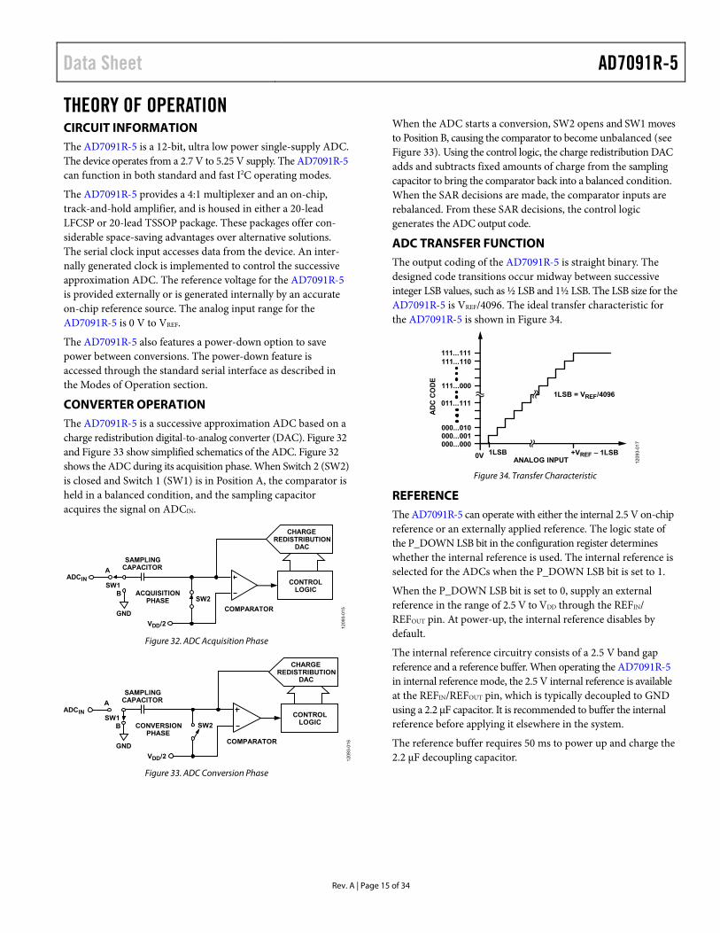
THEORY OF OPERATION CIRCUIT INFORMATION The AD7091R-5 is a 12-bit, ultra low power single-supply ADC. The device operates from a 2.7 V to 5.25 V supply. The AD7091R-5 can function in both standard and fast I2C operating modes.
The AD7091R-5 provides a 4:1 multiplexer and an on-chip, track-and-hold amplifier, and is housed in either a 20-lead LFCSP or 20-lead TSSOP package. These packages offer con-siderable space-saving advantages over alternative solutions. The serial clock input accesses data from the device. An inter-nally generated clock is implemented to control the successive approximation ADC. The reference voltage for the AD7091R-5 is provided externally or is generated internally by an accurate on-chip reference source. The analog input range for the AD7091R-5 is 0 V to VREF.
The AD7091R-5 also features a power-down option to save power between conversions. The power-down feature is accessed through the standard serial interface as described in the Modes of Operation section.
CONVERTER OPERATION The AD7091R-5 is a successive approximation ADC based on a charge redistribution digital-to-analog converter (DAC). Figure 32 and Figure 33 show simplified schematics of the ADC. Figure 32 shows the ADC during its acquisition phase. When Switch 2 (SW2) is closed and Switch 1 (SW1) is in Position A, the comparator is held in a balanced condition, and the sampling capacitor acquires the signal on ADCIN.
CONTROLLOGIC
COMPARATORSW2
SAMPLINGCAPACITOR
ACQUISITIONPHASE
SW1
A
B
GND
CHARGE
DACREDISTRIBUTION
ADCIN
VDD/2
1209
3-01
5
Figure 32. ADC Acquisition Phase
CONTROLLOGIC
COMPARATOR
SW2
SAMPLINGCAPACITOR
CONVERSIONPHASE
SW1
A
B
GND
CHARGE
DACREDISTRIBUTION
ADCIN
VDD/2 1209
3-01
6
Figure 33. ADC Conversion Phase
When the ADC starts a conversion, SW2 opens and SW1 moves to Position B, causing the comparator to become unbalanced (see Figure 33). Using the control logic, the charge redistribution DAC adds and subtracts fixed amounts of charge from the sampling capacitor to bring the comparator back into a balanced condition. When the SAR decisions are made, the comparator inputs are rebalanced. From these SAR decisions, the control logic generates the ADC output code.
ADC TRANSFER FUNCTION The output coding of the AD7091R-5 is straight binary. The designed code transitions occur midway between successive integer LSB values, such as ½ LSB and 1½ LSB. The LSB size for the AD7091R-5 is VREF/4096. The ideal transfer characteristic for the AD7091R-5 is shown in Figure 34.
000...0000V
ADC
CODE
ANALOG INPUT
111...111
000...001000...010
111...110
111...000
011...111
1LSB +VREF – 1LSB
1LSB = VREF/4096
1209
3-01
7
Figure 34. Transfer Characteristic
REFERENCE The AD7091R-5 can operate with either the internal 2.5 V on-chip reference or an externally applied reference. The logic state of the P_DOWN LSB bit in the configuration register determines whether the internal reference is used. The internal reference is selected for the ADCs when the P_DOWN LSB bit is set to 1.
When the P_DOWN LSB bit is set to 0, supply an external reference in the range of 2.5 V to VDD through the REFIN/ REFOUT pin. At power-up, the internal reference disables by default.
The internal reference circuitry consists of a 2.5 V band gap reference and a reference buffer. When operating the AD7091R-5 in internal reference mode, the 2.5 V internal reference is available at the REFIN/REFOUT pin, which is typically decoupled to GND using a 2.2 µF capacitor. It is recommended to buffer the internal reference before applying it elsewhere in the system.
The reference buffer requires 50 ms to power up and charge the 2.2 µF decoupling capacitor.

AD7091R-5 Data Sheet
Rev. A | Page 16 of 34
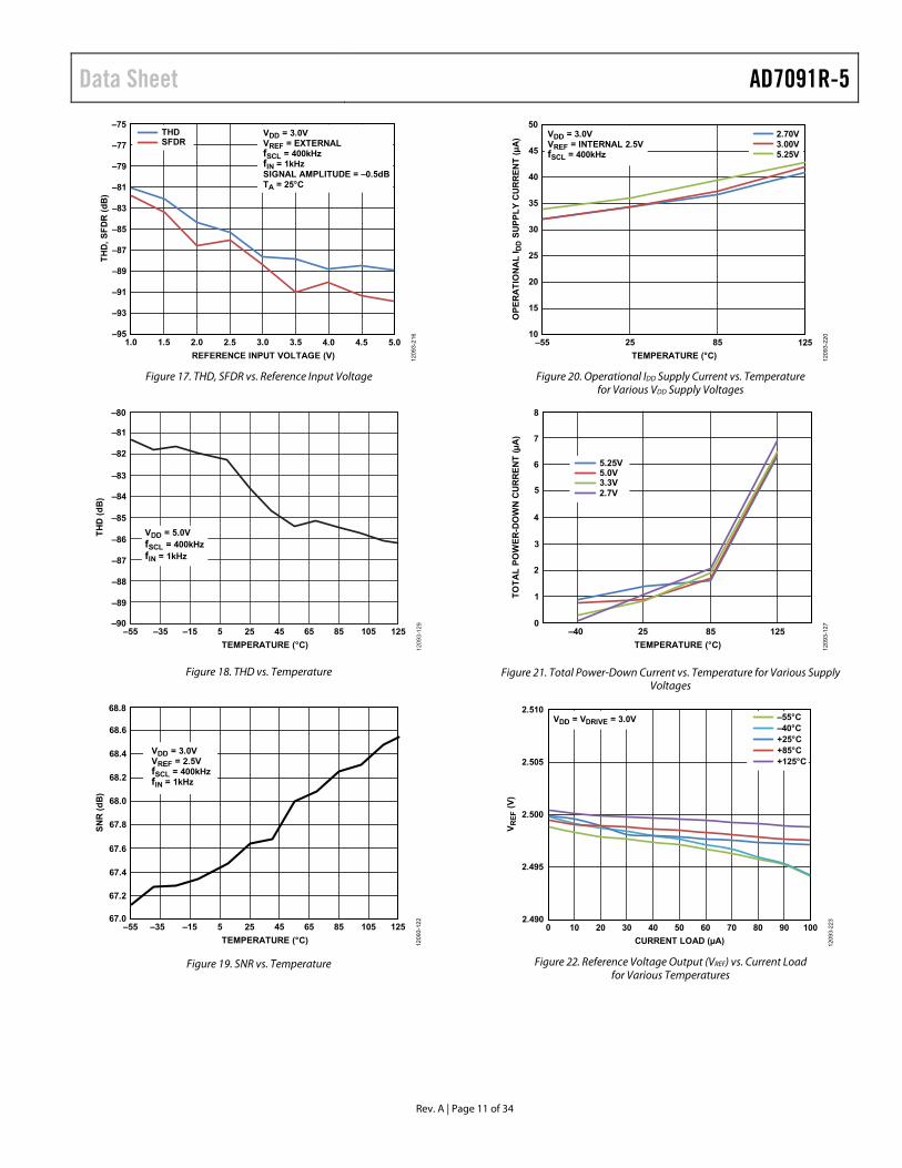
POWER SUPPLY The AD7091R-5 uses two power supply pins: a core supply (VDD) and a digital input/output interface supply (VDRIVE). VDRIVE allows direct interfacing with any logic between 1.8 V and 5.25 V. To reduce the number of supplies needed, VDRIVE and VDD can be tied together depending upon the logic levels of the system. The AD7091R-5 is independent of power supply sequencing between VDRIVE and VDD. Additionally, the AD7091R-5 is insensitive to power supply variations over a wide frequency range, as shown in Figure 25.
The AD7091R-5 powers down automatically at the end of each conversion phase; therefore, the power scales linearly with the sampling rate. The automatic power-down feature makes the AD7091R-5 device ideal for low sampling rates (of even a few hertz) and battery-powered applications.
Table 6. Recommended Power Management Devices1 Product Description ADP7102 20 V, 300 mA, low noise, CMOS LDO ADM7160 Ultralow noise, 200 mA linear regulator ADP162 Ultralow quiescent current, CMOS linear regulator 1 For the latest recommended power management devices, see the AD7091R-5
product page.
DEVICE RESET Upon power-up, a reset pulse of at least 10 ns in width must be provided on the RESET pin to ensure proper initialization of the device. Failure to apply the reset pulse may result in a device malfunction. See Figure 35 for reset pulse timing relative to power supply establishment.
At any time, the RESET pin can reset the device and the contents of all internal registers, including the command register, to their default state. To activate the reset operation, bring the RESET pin low for a minimum of 10 ns while it is asynchronous to the SCL signal. It is imperative that the RESET pin be held at a stable logic level at all times to ensure normal operation.
1209
3-14
1
RESET
VDD
VDRIVE
tRESETPW
tRESET_DELAY
Figure 35. RESET Pin Power Up Timing
ANALOG INPUT Figure 36 shows an equivalent circuit of the analog input structure of the AD7091R-5. The two diodes, D1 and D2, provide ESD protection for the analog input. Ensure that the analog input signal never exceeds the supply rails by more than 300 mV because this causes these diodes to become forward-biased and start conducting current into the substrate. These diodes can conduct a maximum of 10 mA without causing irreversible damage to the device.
D1
D2
R1500Ω
C23.6pF
C1400fF
CONVERSION PHASE SWITCH OPENTRACK PHASE SWITCH CLOSED
D3
VINx
VDDREFIN/
REFOUT
1209
3-01
9
Figure 36. Equivalent Analog Input Circuit
The C1 capacitor in Figure 36 is typically approximately 400 fF and can primarily be attributed to pin capacitance. The R1 resistor is a lumped component made up of the on resistance of a switch. This resistor is typically approximately 500 Ω. The C2 capacitor is the ADC sampling capacitor and typically has a capacitance of 3.6 pF.
In applications where harmonic distortion and SNR are critical, drive the analog inputs from low impedance sources. Large source impedances significantly affect the ac performance of the ADC, which can necessitate using input buffer amplifiers, as shown in Figure 37. The choice of the op amp is a function of the particular application.
When no amplifiers are driving the analog input, limit the source impedance to low values. The maximum source impedance depends on the amount of THD that can be tolerated. The THD increases as the source impedance increases and performance degrades.
Use an external filter on the analog input signal paths to the AD7091R-5 VINx pins to achieve the specified performance. This filter can be a one-pole, low-pass RC filter or similar.
Connect the MUXOUT pin directly to the ADCIN pin. Insert a buffer amplifier in the path, if desired. When sequencing channels, do not place a filter between MUXOUT and the input to any buffer because doing so leads to crosstalk. If a buffer is not implemented, do not place a filter between MUXOUT and ADCIN when sequencing channels because doing so leads to crosstalk.
Data Sheet AD7091R-5
Rev. A | Page 17 of 34
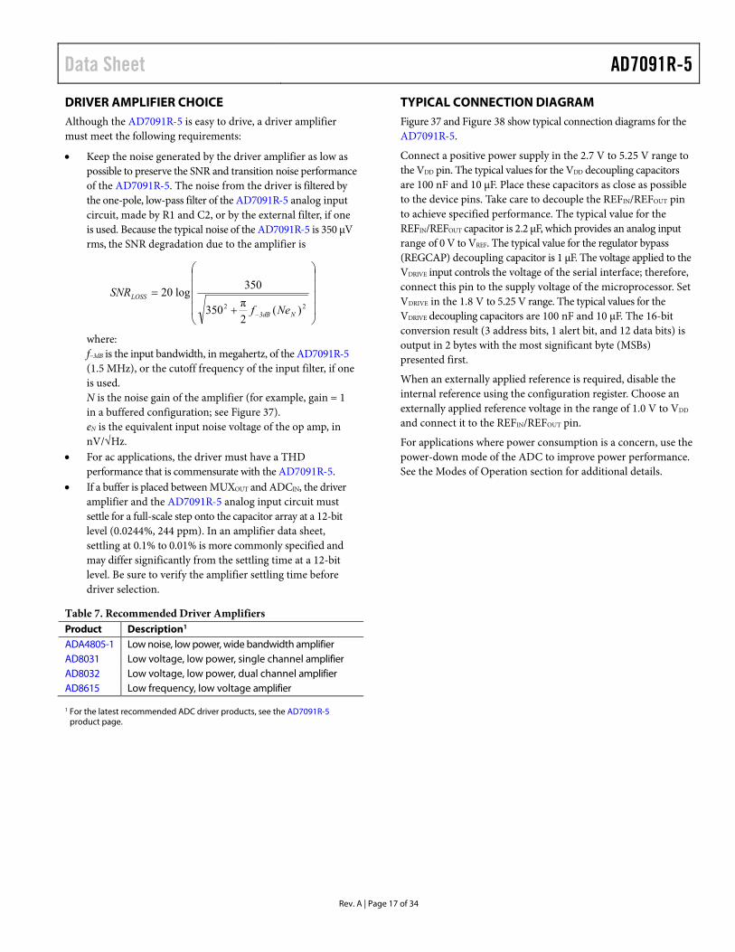
DRIVER AMPLIFIER CHOICE Although the AD7091R-5 is easy to drive, a driver amplifier must meet the following requirements:
• Keep the noise generated by the driver amplifier as low as possible to preserve the SNR and transition noise performance of the AD7091R-5. The noise from the driver is filtered by the one-pole, low-pass filter of the AD7091R-5 analog input circuit, made by R1 and C2, or by the external filter, if one is used. Because the typical noise of the AD7091R-5 is 350 µV rms, the SNR degradation due to the amplifier is
+=
−22 )(
2π350
350log20
N3dB
LOSS
NefSNR
where: f−3dB is the input bandwidth, in megahertz, of the AD7091R-5 (1.5 MHz), or the cutoff frequency of the input filter, if one is used. N is the noise gain of the amplifier (for example, gain = 1 in a buffered configuration; see Figure 37). eN is the equivalent input noise voltage of the op amp, in nV/√Hz.
• For ac applications, the driver must have a THD performance that is commensurate with the AD7091R-5.
• If a buffer is placed between MUXOUT and ADCIN, the driver amplifier and the AD7091R-5 analog input circuit must settle for a full-scale step onto the capacitor array at a 12-bit level (0.0244%, 244 ppm). In an amplifier data sheet, settling at 0.1% to 0.01% is more commonly specified and may differ significantly from the settling time at a 12-bit level. Be sure to verify the amplifier settling time before driver selection.
Table 7. Recommended Driver Amplifiers Product Description1 ADA4805-1 Low noise, low power, wide bandwidth amplifier AD8031 Low voltage, low power, single channel amplifier AD8032 Low voltage, low power, dual channel amplifier AD8615 Low frequency, low voltage amplifier
1 For the latest recommended ADC driver products, see the AD7091R-5 product page.
TYPICAL CONNECTION DIAGRAM Figure 37 and Figure 38 show typical connection diagrams for the AD7091R-5.
Connect a positive power supply in the 2.7 V to 5.25 V range to the VDD pin. The typical values for the VDD decoupling capacitors are 100 nF and 10 µF. Place these capacitors as close as possible to the device pins. Take care to decouple the REFIN/REFOUT pin to achieve specified performance. The typical value for the REFIN/REFOUT capacitor is 2.2 µF, which provides an analog input range of 0 V to VREF. The typical value for the regulator bypass (REGCAP) decoupling capacitor is 1 µF. The voltage applied to the VDRIVE input controls the voltage of the serial interface; therefore, connect this pin to the supply voltage of the microprocessor. Set VDRIVE in the 1.8 V to 5.25 V range. The typical values for the VDRIVE decoupling capacitors are 100 nF and 10 µF. The 16-bit conversion result (3 address bits, 1 alert bit, and 12 data bits) is output in 2 bytes with the most significant byte (MSBs) presented first.
When an externally applied reference is required, disable the internal reference using the configuration register. Choose an externally applied reference voltage in the range of 1.0 V to VDD and connect it to the REFIN/REFOUT pin.
For applications where power consumption is a concern, use the power-down mode of the ADC to improve power performance. See the Modes of Operation section for additional details.

AD7091R-5 Data Sheet
Rev. A | Page 18 of 34
AD7091R-5
SCL
SDA MICROCONTROLLER/MICROPROCESSOR/
DSP
AS1
VIN0
GND
VDD
10µF 100nF 10µF 100nF
REGCAP
1µF
AS0
2.2µF
ANALOGINPUT
47kΩ
VDRIVE
VDRIVE
REFIN/REFOUT
ANALOGINPUT
CONVST/GPO1
ALERT/BUSY/GPO0
VIN3
OPTIONALBUFFER
ADCIN
MUXOUT
560pF
33Ω
1209
3-01
8
Figure 37. Typical Connection Diagram with Optional Buffer
AD7091R-5
SCL
SDA MICROCONTROLLER/MICROPROCESSOR/
DSP
AS1
VIN0
GND
VDD
10µF 100nF 10µF 100nF
REGCAP
1µF
AS0
2.2µF
ANALOGINPUT
33Ω
560pF
47kΩ
VDRIVE
VDRIVE
REFIN/REFOUTANALOG
INPUT
33Ω
560pF
CONVST/GPO1
ALERT/BUSY/GPO0
VIN3ADCIN
MUXOUT
1209
3-14
0
Figure 38. Typical Connection Diagram Without Optional Buffer

Data Sheet AD7091R-5
Rev. A | Page 19 of 34
I2C REGISTERS The AD7091R-5 has several user-programmable registers. Table 9 contains the complete list of registers.
The registers are either read/write (R/W) or read only (R). Data can be written to or read back from the read/write registers. Read only registers can only be read. Any write to a read only register or unimplemented register address is considered no operation (NOP) command, which is an I2C command that the AD7091R-5 ignores. After a write to a read only register, the output on the subsequent I2C frame is all zeros provided that there was no conversion before the next I2C frame. Similarly, any read of an unimplemented register outputs zeros.
ADDRESSING REGISTERS A serial transfer on the AD7091R-5 consists of nine SCL cycles. Data is sent over the serial bus in groups of nine bits—eight bits of data from the transmitter followed by an acknowledge bit from the receiver. Data transitions on the SDA line must occur during the low period of the clock signal and remain stable during the high period. The receiver pulls the SDA line low during the acknowledge bit to signal that the preceding byte has been received correctly. If this is not the case, cancel the transaction. The first byte that the master sends must consist of a 7-bit slave address, followed by a data direction bit. Each device on the bus has a unique slave address; therefore, the first byte sets up communication with a single slave device for the duration of the transaction.
The transaction can be used either to write to a slave device (data direction bit = 0) or to read data from it (data direction bit = 1). In the case of a read transaction, it is often necessary to first write to the slave device (in a separate write transaction) to tell it from which register to read. Reading and writing cannot be combined in one transaction.
When the transaction is complete, the master can maintain control of the bus, initiating a new transaction by generating another start bit (high to low transition on SDA while SCL is high). This is known as a repeated start. Alternatively, the bus can be relinquished by releasing the SCL line followed by the SDA line. This low to high transition on SDA while SCL is high is known as a stop bit (P), and it leaves the I2C bus in its idle state (no current is consumed by the bus).
SLAVE ADDRESS The first byte that the user writes to the device is the slave address byte. The AD7091R-5 has a 7-bit slave address. On the AD7091R-5, the three MSBs of the 7-bit slave address are fixed to 3’b010. The four LSBs are set by the user via external pins. Two address select pins are on each device, and high, low, or no connect can be detected on each pin, giving nine combinations.
Table 8 shows the four LSBs of the slave address for the AD7091R-5 for different configurations of the address select pins.
Table 8. Slave Addresses AS1
1 AS0
1 A3 A2 A1 A0
VDD VDD 0 0 0 0 VDD NC 0 0 1 0 VDD GND 0 0 1 1 NC VDD 1 0 0 0 NC NC 1 0 1 0 NC GND 1 0 1 1 GND VDD 1 1 0 0 GND NC 1 1 1 0 GND GND 1 1 1 1
1 NC means leave the ASx pins floating, VDD means pulled high, and GND means pulled low.
I2C REGISTER ACCESS
Table 9. Register Descriptions Address Register Name Default Access 0x00 Conversion result 0x0000 R 0x01 Channel 0x0000 R/W 0x02 Configuration 0x00C0 R/W 0x03 Alert indication 0x0000 R 0x04 Channel 0 low limit 0x0000 R/W 0x05 Channel 0 high limit 0x01FF R/W 0x06 Channel 0 hysteresis 0x01FF R/W 0x07 Channel 1 low limit 0x0000 R/W 0x08 Channel 1 high limit 0x01FF R/W 0x09 Channel 1 hysteresis 0x01FF R/W 0x0A Channel 2 low limit 0x0000 R/W 0x0B Channel 2 high limit 0x01FF R/W 0x0C Channel 2 hysteresis 0x01FF R/W 0x0D Channel 3 low limit 0x0000 R/W 0x0E Channel 3 high limit 0x01FF R/W 0x0F Channel 3 hysteresis 0x01FF R/W

AD7091R-5 Data Sheet
Rev. A | Page 20 of 34
CONVERSION RESULT REGISTER The conversion result register is a 16-bit, read only register that stores the results from the most recent ADC conversion in straight binary format. The channel ID of the converted channel and the alert status are also included in this register.
Rese rved 12 -b it Conve rs ion result
2 -b it Channe l ID Ale rt flag
1: Ale rt has occured .0 : No Ale rt.
0
01
02
03
04
05
06
07
08
09
010
011
012
013
014
015
0
[ 15 ] RSV ( R) [ 11 :0 ] CO N V_RESULT ( R)
[ 14 :13 ] CH _ID ( R) [ 12 ] ALERT ( R)
Table 10. Conversion Result Bit Map MSB LSB B15 B14 B13 B12 B11 B10 B9 B8 B7 B6 B5 B4 B3 B2 B1 B0 RSV CH_ID ALERT CONV_RESULT
Table 11. Bit Descriptions for the Conversion Result Register Bit(s) Name Description Reset Access 15 RSV Reserved 0x0 R [14:13] CH_ID 2-bit channel ID of the channel converted 0x0 R B14 B13 Analog Input Channel
0 0 Channel 0 0 1 Channel 1 1 0 Channel 2 1 1 Channel 3
12 ALERT Alert flag 0x0 R 0: no alert occurred 1: alert has occurred [11:0] CONV_RESULT 12-bit conversion result 0x000 R
Data Sheet AD7091R-5
Rev. A | Page 21 of 34
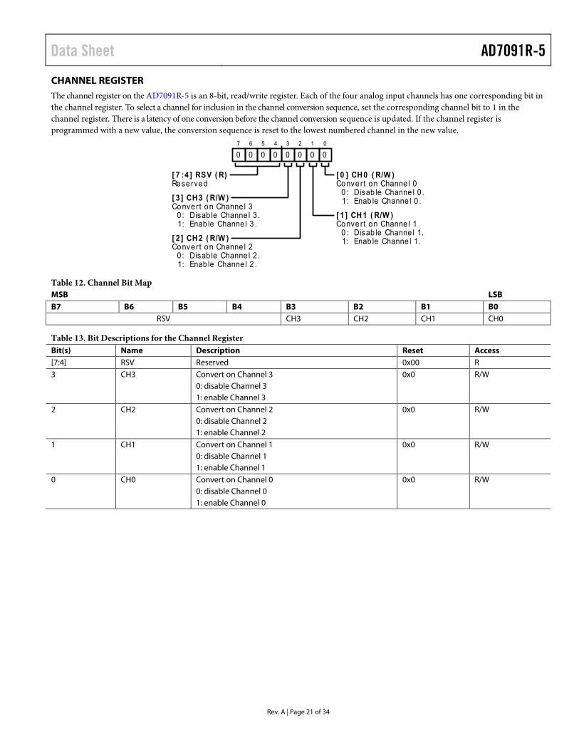
CHANNEL REGISTER The channel register on the AD7091R-5 is an 8-bit, read/write register. Each of the four analog input channels has one corresponding bit in the channel register. To select a channel for inclusion in the channel conversion sequence, set the corresponding channel bit to 1 in the channel register. There is a latency of one conversion before the channel conversion sequence is updated. If the channel register is programmed with a new value, the conversion sequence is reset to the lowest numbered channel in the new value.
Rese rved Conve rt on Channe l 0
1: Enab le Channe l 0 .0 : Disab le Channe l 0 .
Conve rt on Channe l 3
1: Enab le Channe l 3 .0 : Disab le Channe l 3 .
Conve rt on Channe l 1
1: Enab le Channe l 1.0 : Disab le Channe l 1.
Conve rt on Channe l 2
1: Enab le Channe l 2 .0 : Disab le Channe l 2 .
0
01
02
03
04
05
06
07
0
[ 7 :4 ] RSV ( R) [ 0 ] CH 0 ( R/W )
[ 3 ] CH 3 ( R/W )
[ 1 ] CH 1 ( R/W )
[ 2 ] CH 2 ( R/W )
Table 12. Channel Bit Map MSB LSB B7 B6 B5 B4 B3 B2 B1 B0
RSV CH3 CH2 CH1 CH0
Table 13. Bit Descriptions for the Channel Register Bit(s) Name Description Reset Access [7:4] RSV Reserved 0x00 R 3 CH3 Convert on Channel 3 0x0 R/W 0: disable Channel 3 1: enable Channel 3 2 CH2 Convert on Channel 2 0x0 R/W 0: disable Channel 2 1: enable Channel 2 1 CH1 Convert on Channel 1 0x0 R/W 0: disable Channel 1 1: enable Channel 1 0 CH0 Convert on Channel 0 0x0 R/W 0: disable Channel 0 1: enable Channel 0

AD7091R-5 Data Sheet
Rev. A | Page 22 of 34
CONFIGURATION REGISTER The configuration register is a 16-bit, read/write register that sets the operating modes of the AD7091R-5.
D r iv e Ty p e o f ALERT/BU SY/GPO 0 p in
1 :ty p e .ALERT/BU SY/GPO 0 p in is o f CMO S d r iv e
0 :d r iv e ty p e .ALERT/BU SY/GPO 0 p in is o f o p e n- d r a in
Po w e r D o w n m o d e
11: M o d e 3 .10 : M o d e 2 .0 1: M o d e 1 .0 0 : M o d e 0 .
Va lue a t GPO 2
1: D r iv e '1 ' o n GPO 2 p in .0 : D r iv e '0 ' o n GPO 2 p in .
Va lue a t GPO 1
1: D r iv e '1 ' o n GPO 1 p in .0 : D r iv e '0 ' o n GPO 1 p in .
Re s e r v e d Po lar ity o f ALERT/BU SY/GPO 0 p in ( if ALERT_ENis 1) o r v a lue a t GPO 0
1:is 1 ) o r GPO 0 = 1 .Ac t iv e H IGH ALERT Po lar ity ( if ALERT_EN
0 :is 1 ) o r GPO 0 = 0 .Ac t iv e LO W ALERT Po lar ity ( if ALERT_EN
Re s e r v e d
Enab le ALERT o r GPO 0
0 :a GPO .ALERT/BU SY/GPO 0 p in w ill b e us e d as
1:s ta tus .ALERT/BU SY/GPO 0 p in is us e d fo r ALERT/BU SY
Enab le Glitc h Filte r o n SD A/SCL
1: By p as s the Glitc h- Filte r .
0 :line s .Enab le '50 ns ' Glitc h- f ilte r ing o n SD A/SCL
ALERT/BU SY/GPO 0 p in ind ic a te s if thep ar t is b us y c o nv e r t ing
1:
th is w ill a lw ay s b e r e ad - b ac k as 0 .s ta tus p r o v id e d ALERT_EN is 1 . Els e ,ALERT/BU SY/GPO 0 p in is us e d fo r BU SY
0 :BU SY s ta tus .ALERT/BU SY/GPO 0 p in is no t us e d fo r
Co m m and Mo d e
1:m o d e ( if AU TO = 1 )Co m m and m o d e ( if AU TO = 0 ) o r Sam p le
0 :m o d e ( if AU TO = 1 )Sam p le m o d e ( if AU TO = 0 ) o r Auto c y c le
Tim e r v a lue fo r Auto c y c le m o d e
11: 8 0 0 uS.10 : 4 0 0 uS.0 1: 2 0 0 uS.0 0 : 10 0 uS.
So f tw ar e Re s e t b it
1 : Ac t iv a te So f t - Re s e t .0 : So f t - Re s e t no t ac t iv e .
Au to c y c le Mo d e
1:m o d e ( if CMD = 1 )Au to - c y c le m o d e ( if CMD = 0 ) o r Sam p le
0 :m o d e ( if CMD = 1 )Sam p le m o d e ( if CMD = 0 ) o r Co m m and
0
0
1
0
2
0
3
0
4
0
5
0
6
1
7
1
8
0
9
0
1 0
0
1 1
0
1 2
0
1 3
0
1 4
0
1 5
0
[ 1 5 ] A L ER T _D R IV E_T YP E ( R /W ) [ 1 : 0 ] P _D O W N ( R /W )
[ 1 4 ] G P O 2 ( R /W ) [ 2 ] G P O 1 ( R /W )
[ 1 3 ] R S V ( R ) [ 3 ] A L ER T _P O L _o r _G P O 0 ( R /W )
[ 1 2 ] R S V ( R )
[ 4 ] A L ER T _EN _o r _G P O 0 ( R /W )
[ 1 1 ] F L T R ( R /W )
[ 5 ] B U S Y ( R /W )
[ 1 0 ] C M D ( R /W )
[ 7 : 6 ] C y c le _t im e r ( R /W )
[ 9 ] S R S T ( R /W )
[ 8 ] A U T O ( R /W )
Table 14. Configuration Bit Map MSB LSB B15 B14 B13 B12 B11 B10 B9 B8 B7 B6 B5 B4 B3 B2 B1 B0 ALERT_DRIVE_TYPE
GPO2 RSV RSV FLTR CMD SRST AUTO CYCLE_ TIMER
BUSY ALERT_EN_OR_GPO0
ALERT_ POL_OR_ GPO0
GPO1 P_DOWN
Table 15. Bit Descriptions for the Configuration Register1 Bit(s) Name Description Reset Access 15 ALERT_DRIVE_TYPE Drive the type of the ALERT/BUSY/GPO0 pin. 0x0 RW 0: the ALERT/BUSY/GPO0 pin is open-drain drive type. 1: the ALERT/BUSY/GPO0 pin is CMOS drive type. 14 GPO2 Value at GPO2. 0x0 RW 0: drive 0 on GPO2 pin. 1: drive 1 on GPO2 pin. 13 RSV Reserved. 0x00 R 12 RSV Reserved. 0x00 R

Data Sheet AD7091R-5
Rev. A | Page 23 of 34
Bit(s) Name Description Reset Access 11 FLTR Enable the glitch filter on SDA/SCL. 0x0 RW 0: enable 50 ns glitch filtering on the SDA/SCL lines. 1: bypass the glitch filter. 10 CMD Command mode. 0x0 RW 0: sample mode (if AUTO = 0) or autocycle mode (if AUTO = 1). 1: command mode (if AUTO = 0) or sample mode (if AUTO = 1). 9 SRST Software reset bit. Setting this bit resets the internal digital control logic, the conversion
result and alert indication registers, but not the other memory-mapped registers. This bit is automatically cleared in the next clock cycle.
0x0 RWAC
0: soft reset not active. 1: activate soft reset. 8 AUTO Autocycle mode. 0x0 RW 0: sample mode (if CMD = 0) or command mode (if CMD = 1). 1: autocycle mode (if CMD = 0) or sample mode (if CMD = 1). [7:6] CYCLE_TIMER Timer value for autocycle mode. 0x3 RW 00: 100 μs. 01: 200 μs. 10: 400 μs. 11: 800 μs. 5 BUSY ALERT/BUSY/GPO0 pin indicates if the device is busy converting. 0x0 RW 0: the ALERT/BUSY/GPO0 pin is not used for the busy status. 1: the ALERT/BUSY/GPO0 pin is used for the busy status provided
ALERT_EN_OR_GPO0 is 1. Otherwise, this bit is always read back as 0.
4 ALERT_EN_OR_GPO0 Enable the ALERT/BUSY/GPO0 pin or GPO0. 0x0 RW 1: the ALERT/BUSY/GPO0 pin is used for the ALERT/BUSY status. 0: the ALERT/BUSY/GPO0 pin is used as a GPO. 3 ALERT_POL_OR_GPO0 Polarity of the ALERT/BUSY/GPO0 pin (if ALERT_EN_OR_GPO0 is 1) or value at GPO0. 0x0 RW 0: active low ALERT/BUSY/GPO0 polarity (if ALERT_EN_OR_GPO0 is 1) or GPO0 = 0. 1: active high ALERT/BUSY/GPO0 polarity (if ALERT_EN_OR_GPO0 is 1) or GPO0 = 1. 2 GPO1 Value at GPO1. 0x0 RW 0: drive 0 on the CONVST/GPO1 pin.
1: drive 1 on the CONVST/GPO1 pin.
[1:0] P_DOWN Power-down modes. 0x0 R/W Setting Mode Sleep Mode/Bias Generator Internal Reference
00 Mode 0 Off Off 01 Mode 1 Off On 10 Mode 2 On Off 11 Mode 3 On On 1 The AD7091R-5 supports the I2C standard glitch filter, but does not support clock stretching or general call addressing.

AD7091R-5 Data Sheet
Rev. A | Page 24 of 34
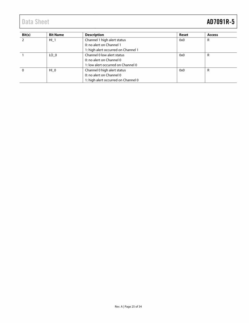
ALERT INDICATION REGISTER The 8-bit alert indication register is a read only register that provides information on an alert event. If a conversion result activates the ALERT/BUSY/GPO0 pin, as described in the Channel x Low Limit Register section and the Channel x High Limit Register section, read the alert register to determine the source of the alert. The register contains two status bits per channel, one corresponding to the high limit, and the other to the low limit. The bit with a status equal to 1 shows where the violation occurred, that is, on which channel, and whether the violation occurred on the upper or lower limit. If a second alert event occurs on another channel between receiving the first alert and interrogating the alert register, the corresponding bit for that alert event is also set.
The contents of the alert indication register are reset by reading it. When the AD7091R-5 uses the I2C interface to read the alert indication register, the register is reset at the fourth SCL clock of the byte. By this time, the data from the register has moved to the I2C shift register.
The alert bits for any unimplemented channels always return zeros.
Low ale rt Channe l 3
1: Low ale rt occurred on Channe l 3 .0 : No ale rt on Channe l 3 .
High ale rt Channe l 0
1: High ale rt occurred on Channe l 0 .0 : No ale rt on Channe l 0 .
High ale rt Channe l 3
1: High ale rt occurred on Channe l 3 .0 : No ale rt on Channe l 3 .
Low ale rt Channe l 0
1: Low ale rt occurred on Channe l 0 .0 : No ale rt on Channe l 0 .
Low ale rt Channe l 2
1: Low ale rt occurred on Channe l 2 .0 : No ale rt on Channe l 2 .
High ale rt Channe l 1
1: High ale rt occurred on Channe l 1.0 : No ale rt on Channe l 1.
High ale rt Channe l 2
1: High ale rt occurred on Channe l 2 .0 : No ale rt on Channe l 2 .
Low ale rt Channe l 1
1: Low ale rt occurred on Channe l 1.0 : No ale rt on Channe l 1.
0
01
02
03
04
05
06
07
0
[ 7 ] Lo _3 ( R) [ 0 ] H i_0 ( R)
[ 6 ] H i_3 ( R) [ 1 ] Lo _0 ( R)
[ 5 ] Lo _2 ( R) [ 2 ] H i_1 ( R)
[ 4 ] H i_2 ( R) [ 3 ] Lo _1 ( R)
Table 16. Alert Indication Bit Map
Table 17. Bit Descriptions for the Alert Indication Register Bit(s) Bit Name Description Reset Access 7 LO_3 Channel 3 low alert status 0x0 R 0: no alert on Channel 3 1: low alert occurred on Channel 3 6 HI_3 Channel 3 high alert status 0x0 R 0: no alert on Channel 3 1: high alert occurred on Channel 3 5 LO_2 Channel 2 low alert status 0x0 R 0: no alert on Channel 2 1: low alert occurred on Channel 2 4 HI_2 Channel 2 high alert status 0x0 R 0: no alert on Channel 2 1: high alert occurred on Channel 2 3 LO_1 Channel 1 low alert status 0x0 R 0: no alert on Channel 1 1: low alert occurred on Channel 1
MSB LSB B7 B6 B5 B4 B3 B2 B1 B0 LO_3 HI_3 LO_2 HI_2 LO_1 HI_1 LO_0 HI_0
Data Sheet AD7091R-5
Rev. A | Page 25 of 34
Bit(s) Bit Name Description Reset Access 2 HI_1 Channel 1 high alert status 0x0 R 0: no alert on Channel 1 1: high alert occurred on Channel 1 1 LO_0 Channel 0 low alert status 0x0 R 0: no alert on Channel 0 1: low alert occurred on Channel 0 0 HI_0 Channel 0 high alert status 0x0 R 0: no alert on Channel 0 1: high alert occurred on Channel 0

AD7091R-5 Data Sheet
Rev. A | Page 26 of 34
CHANNEL x LOW LIMIT REGISTER Each analog input channel of the AD7091R-5 has its own low limit register. The low limit registers are 16-bit read/write registers. See Table 9 for the register addresses. The low limit registers store the lower limit of the conversion value that activates the ALERT output.
Of the 16 bits, only the twelve least significant bits (LSBs) are used, Bit B11 to Bit B0. Bit B15 to Bit B12 are not used.
CHANNEL x HIGH LIMIT REGISTER Each analog input channel of the AD7091R-5 has its own high limit register. The high limit registers are 16-bit read/write registers. See Table 9 for the register addresses. The high limit registers store the upper limit of the conversion value that activates the ALERT output.
Of the 16 bits, only the twelve least significant bits (LSBs) are used, Bit B11 to Bit B0. Bit B15 to Bit B12 are not used.
CHANNEL x HYSTERESIS REGISTER Each analog input channel of the AD7091R-5 has its own hysteresis register, which are 16-bit read/write registers. See Table 9 for the register addresses. The hysteresis register stores the hysteresis value (N) when using the limit registers. The hysteresis value determines the reset point for the ALERT/ BUSY/GPO0 pin if a violation of the limits has occurred.
Of the 16 bits, only the twelve least significant bits (LSBs) are used, Bit B11 to Bit B0. Bit B15 to Bit B12 are not used.
Table 18. Channel x Low Limit Bit Map MSB LSB B15 B14 B13 B12 B11 B10 B9 B8 B7 B6 B5 B4 B3 B2 B1 B0
RSV CHx LOW LIMIT
Table 19. Bit Descriptions for Channel x Low Limit Register Bits Bit Name Description Reset Access [15:12] RSV Reserved 0x00 R [11:0] CHx LOW LIMIT Low limit value for Channel x 0x000 R/W
Table 20. Channel x High Limit Bit Map MSB LSB B15 B14 B13 B12 B11 B10 B9 B8 B7 B6 B5 B4 B3 B2 B1 B0
RSV CHx HIGH LIMIT
Table 21. Bit Descriptions for Channel x High Limit Register Bits Bit Name Description Reset Access [15:12] RSV 0x00 R [11:0] CHx HIGH LIMIT High limit value for Channel x 0xFFF R/W
Table 22. Channel x Hysteresis Bit Map MSB LSB B15 B14 B13 B12 B11 B10 B9 B8 B7 B6 B5 B4 B3 B2 B1 B0
RSV CHx HYSTERISIS
Table 23. Bit Descriptions for the Channel x Hysteresis Register Bits Bit Name Description Reset Access [15:12] RSV 0x00 R [11:0] CHx HYSTERISIS Hysteresis value for Channel x 0xFFF R/W

Data Sheet AD7091R-5
Rev. A | Page 27 of 34
I2C INTERFACE Control of the AD7091R-5 is carried out via the I2C-compatible serial bus. The AD7091R-5 is connected to this bus as a slave device under the control of a master device such as the processor.
SERIAL BUS ADDRESS BYTE The first byte that the user writes to the device is the slave address byte. Similar to all I2C-compatible devices, the AD7091R-5 has a 7-bit serial address. The three MSBs of this address are set to 010. The four LSBs are user programmable by the three-state input pins, AS0 and AS1, as shown in Table 24.
In Table 24, high means tie the pin to VDRIVE, low means tie the pin to GND, and NC refers to a pin left floating. Note that in NC cases, the stray capacitance on the pin must be less than 30 pF to allow correct detection of the floating state; therefore, any printed circuit board trace must be kept as short as possible.
Table 24. Slave Address Control Using Three-State Input Pins
AS1 AS0 Slave Address (A6 to A0)
Binary Hex High High 010 0000 0x20 High NC 010 0010 0x22 High Low 010 0011 0x23 NC H 010 1000 0x28 NC NC 010 1010 0x2A NC Low 010 1011 0x2B Low High 010 1100 0x2C Low NC 010 1110 0x2E Low Low 010 1111 0x2F
GENERAL I2C TIMING Figure 39 shows the timing diagram for general read and write operations using an I2C compliant interface.
When no device is driving the bus, both SCL and SDA are high. This is known as the idle state. When the bus is idle, the master initiates a data transfer by establishing a start condition, defined
as a high to low transition on the serial data line (SDA) while the serial clock line (SCL) remains high. This indicates that a data stream follows. The master device must generate the clock.
Data is sent over the serial bus in groups of nine bits—eight bits of data from the transmitter are followed by an acknowledge bit (ACK) from the receiver. Data transitions on the SDA line must occur during the low period of the clock signal and remain stable during the high period. The receiver must pull the SDA line low during the acknowledge bit to signal that the preceding byte has been received correctly. If this is not the case, cancel the transaction.
The first byte that the master sends must consist of a 7-bit slave address, followed by a data direction bit. Each device on the bus has a unique slave address; therefore, the first byte sets up communication with a single slave device for the duration of the transaction.
The transaction can be used either to write to a slave device (data direction bit = 0) or to read data from it (data direction bit = 1). In the case of a read transaction, it is often necessary first to write to the slave device (in a separate write transaction) to tell it from which register to read. Reading and writing cannot be combined in one transaction.
When the transaction is complete, the master can maintain control of the bus, initiating a new transaction by generating another start bit (high to low transition on SDA while SCL is high). This is known as a repeated start (SR). Alternatively, the bus can be relinquished by releasing the SCL line followed by the SDA line. This low to high transition on SDA while SCL is high is known as a stop bit (P), and it leaves the I2C bus in its idle state (no current is consumed by the bus).
The example in Figure 39 shows a simple write transaction with an AD7091R-5 as the slave device. In this example, the AD7091R-5 register pointer is being set up for a future read transaction.
P7 P6 P5 P4 P3 P2 P1 P0
START CONDBY MASTER
ACK. BYAD7091R-5
SLAVE ADDRESS BYTE ACK. BYAD7091R-5
SCL
SDA
REGISTER ADDRESS STOP BYMASTER
USER PROGRAMMABLE4 LSBs
R/WA6 A5 A4 A3 A2 A1 A0
1209
3-04
0
Figure 39. General I2C Timing

AD7091R-5 Data Sheet
Rev. A | Page 28 of 34
WRITING TO THE AD7091R-5 WRITING TWO BYTES OF DATA TO A 16-BIT REGISTER With the exception of the channel register, all registers on the AD7091R-5 are 16-bit registers; therefore, two bytes of data are required to write a value to any one of these registers. Writing two bytes of data to a register consists of the following sequence (see Figure 40):
1. The master device asserts a start condition on SDA. 2. The master sends the 7-bit slave address followed by the
write bit (low). 3. The addressed slave device asserts an acknowledge on SDA. 4. The master sends a register address. The slave asserts an
acknowledge on SDA. 5. The master sends the first data byte (most significant). 6. The slave asserts an acknowledge on SDA. 7. The master sends the second data byte (least significant). 8. The slave asserts an acknowledge on SDA. 9. The master asserts a stop condition on SDA to end the
transaction.
WRITING TO MULTIPLE REGISTERS Writing to multiple address registers consists of the following steps (see Figure 41):
1. The master device asserts a start condition on SDA. 2. The master sends the 7-bit slave address followed by
the write bit (low). 3. The addressed slave device (AD7091R-5) asserts an
acknowledge on SDA. 4. The master sends a register address, for example, the
configuration register address. 5. The slave asserts an acknowledge on SDA. 6. The master sends the first data byte. 7. The slave asserts an acknowledge on SDA. 8. The master sends the second data byte. 9. The slave asserts an acknowledge on SDA. 10. The master sends a second register address, for example,
the Channel 0 high limit register. 11. The slave asserts an acknowledge on SDA. 12. The master sends the first data byte. 13. The slave asserts an acknowledge on SDA. 14. The master sends the second data byte. 15. The slave asserts an acknowledge on SDA. 16. The master asserts a stop condition on SDA to end the
transaction.
S SLAVE ADDRESS 0 SA REG POINTER SA DATA[15:8] SA PDATA[7:0] SA
FROM MASTER TO SLAVE
FROM SLAVE TO MASTER
S = START CONDITIONSR = REPEATED STARTP = STOP CONDITIONSA = SLAVE ACKNOWLEDGEA = NOT ACKNOWLEDGE 12
093-
059
Figure 40. Writing Two Bytes of Data to a 16-Bit Register
S
...
...0 SA SASLAVE ADDRESS POINT TO CONFIG REG (0x02)
PSASASA DATA[7:0]DATA[15:8]POINT TO CH0 HIGH LIMIT (0x05)
DATA[15:8] SA SADATA[7:0]
FROM MASTER TO SLAVE
FROM SLAVE TO MASTER
S = START CONDITIONSR = REPEATED STARTP = STOP CONDITIONSA = SLAVE ACKNOWLEDGEA = NOT ACKNOWLEDGE 12
093-
060
Figure 41. Writing to Multiple Registers

Data Sheet AD7091R-5
Rev. A | Page 29 of 34
READING DATA FROM THE AD7091R-5 READING TWO BYTES OF DATA FROM A 16-BIT REGISTER Reading the contents from any of the 16-bit registers is a 2-byte read operation. In this protocol, the first part of the transaction writes to the register pointer. When the register address has been set up, any number of reads can be performed from that particular register without writing to the address pointer register again. When the required number of reads is complete, the master must not acknowledge the final byte. This tells the slave to stop transmitting, allowing a stop condition to be asserted by the master. Further reads from this register can be performed in a future transaction without rewriting to the register pointer.
If a read from a different address is required, the relevant register address must be written to the address pointer register and, again, any number of reads from this register can then be performed. In the following example, the master device reads three lots of 2-byte data from a slave device, but as many lots consisting of two bytes can be read as required. This protocol assumes that the particular register address has been set up by a single-byte write operation to the address pointer register.
Reading two bytes of data from a 16-bit register consists of the following sequence (see Figure 42):
1. The master device asserts a start condition on SDA. 2. The master sends the 7-bit slave address followed by the
read bit (high). 3. The addressed slave device asserts an acknowledge on SDA. 4. The master receives the data byte. 5. The master asserts an acknowledge on SDA. 6. The master receives the second data byte. 7. The master asserts an acknowledge on SDA. 8. The master receives the data byte. 9. The master asserts an acknowledge on SDA. 10. The master receives the second data byte. 11. The master asserts an acknowledge on SDA. 12. The master receives the data byte. 13. The master asserts an acknowledge on SDA. 14. The master receives the second data byte. 15. The master asserts a not acknowledge on SDA to notify the
slave that the data transfer is complete. 16. The master asserts a stop condition on SDA to end the
transaction.
S A
P...
...1 A
A
A A A
A
SLAVE ADDRESS
DATA[7:0]
DATA[7:0] DATA[7:0]
DATA[15:8]
DATA[15:8] DATA[15:8]
FROM MASTER TO SLAVE
FROM SLAVE TO MASTER
S = START CONDITIONSR = REPEATED STARTP = STOP CONDITIONA = ACKNOWLEDGEA = NOT ACKNOWLEDGE 12
093-
061
Figure 42. Reading Three Lots of Two Bytes of Data from the Conversion Result Register (Conversion Register Pointer Already Set)
AD7091R-5 Data Sheet
Rev. A | Page 30 of 34
MODES OF OPERATION There are three methods of initiating a conversion on the AD7091R-5 with the I2C interface: sample mode using the CONVST/GPO1 pin, command mode, and autocycle mode. In the CONVST/GPO1 pin mode, conversions are done on demand. Whenever the CONVST/GPO1 pin is toggled, an ADC conversion happens. In command mode, the read of the conversion result register starts the conversion. In autocycle mode, conversions occur on the selected channels in the background periodically. This mode monitors whether signals cross certain threshold levels, the absolute value being relatively unimportant.
SAMPLE MODE At power-up, the device wakes up in sample mode and selects Channel 0 for conversion. Sample mode can be selected subse-quently by writing a value of 0 to both the CMD and auto bits of the configuration register or by writing a value of 1 to both the CMD and auto bits. In sample mode, conversions are controlled by toggling the active low CONVST/GPO1 pin.
To perform conversion on a channel other than Channel 0 or on a sequence of channels, before initiating any conversion, write to the channel register to select the channels for conversion. On each CONVST pulse, the next channel in the selected sequence is converted starting from the lowest numbered channel selected (0, 1 … 7).
A high to low transition on the CONVST/GPO1 pin puts the track-and-hold circuit into hold mode and samples the analog input. The conversion is initiated and requires approximately 550 ns to complete. When the conversion process is finished, the track-and-hold circuit goes back into track.
To read back data stored in the conversion result register, first wait until the conversion is finished. If the address pointer is pointing to the conversion result register, the conversion data can be read using the protocol described in Figure 42. Otherwise, the address pointer must be set to point at the conversion result register before conversion data can be read. When the conversion result read is completed, the user may pull the CONVST pin low again to start another conversion.
Do not toggle the CONVST pin when activity is occurring on the I2C bus.
COMMAND MODE In command mode, the AD7091R-5 converts on demand on either a single channel or a sequence of channels. This mode of operation allows a conversion to be selected automatically any time a write operation occurs to the command register. In command mode, the AD7091R-5 converts the next programmed channel when the conversion result register is read. To enter this mode, the required combination of channels is written into the channel register. Select command mode operation by writing CMD = 1 and auto = 0 in the configuration register. Following the write operation, the AD7091R-5 must be addressed again to indicate that a read operation is required from the conversion result register.
The conversion starts on the first positive edge of SCL after the ACK for the previous byte is sent to avoid starting a conversion during the ACK cycle. This does not create an issue with the exact time that the conversion data must be sent on the I2C bus because the first three bits sent on the I2C bus correspond to the channel for which the conversion data belongs. After the conversion is completed, the ADC powers down. The next conversion in the sequence starts after a subsequent read from the conversion result register is initiated. The device cycles through the selected channels from the lowest selected channel number in the sequence to the next until all channels in the sequence are converted. After all channels in the sequence are converted, the sequence rolls back to the lowest numbered channel enabled so that the sequence can be repeated indefinitely.
To stop converting in the command mode, the master does not acknowledge the final byte of data. This NACK stops the AD7091R-5 transmission, allowing the master to assert a stop condition on the bus. On the receipt of an I2C NACK condition, the AD7091R-5 stops converting, but the content of the configuration register is preserved. After the device is readdressed and a read initiated from the conversion result register, the AD7091R-5 begins converting on the previously selected sequence of channels.
The conversion sequence starts at the first selected channel in the sequence. That is, if Channel 1, Channel 2, and Channel 3 are selected and a stop condition occurs after the result for Channel 1 is read, on the resumption of conversions, Channel 2 is converted and the conversion sequence continues. This happens provided the channel register is not written in between conversions. However, if the channel register is written, this results in the conversion starting from Channel 1.

Data Sheet AD7091R-5
Rev. A | Page 31 of 34
The example in Figure 43 shows command mode converting on a sequence of channels including Channel 0, Channel 1, and Channel 2.
1. The master device asserts a start condition on SDA. 2. The master sends the 7-bit slave address followed by the
write bit (low). 3. The addressed slave device (AD7091R-5) asserts an
acknowledge on SDA. 4. The master sends the configuration register address (0x02). 5. The slave asserts an acknowledge on SDA. 6. The master sends the first data byte (0x06) to the
configuration register, which selects the command mode. 7. The slave asserts an acknowledge on SDA. 8. The master sends the second data byte (0x00) to the
configuration register. 9. The slave asserts an acknowledge on SDA. 10. The master sends the channel register address (0x01). 11. The slave asserts an acknowledge on SDA. 12. The master sends the data byte (0x07) to the channel register,
which selects Channel 0, Channel 1, and Channel 2. 13. The slave asserts an acknowledge on SDA. 14. The master sends the conversion result register address (0x00). 15. The slave asserts an acknowledge on SDA. 16. The master sends a repeated start and the 7-bit slave
address followed by the read bit (high).
17. The slave (AD7091R-5) asserts an acknowledge on SDA. 18. The master receives a data byte, which contains the
channel address bits, the alert bit, and the four MSBs of the converted result for Channel 0.
19. The master then asserts an acknowledge on SDA. 20. The master receives the second data byte, which contains
the eight LSBs of the converted result for Channel 0. The master then asserts on acknowledge on SDA.
21. Step 18 to Step 20 repeat for Channel 1 and Channel 2. 22. After the master has received the results from all the
selected channels, the slave again converts and outputs the result for the first channel in the selected sequence. Step 18 to Step 21 are repeated.
23. The master asserts a not acknowledge on SDA and a stop condition on SDA to end the conversion and exit command mode.
To change the conversion sequence, rewrite a new sequence to the command mode. If a new write to the channel register is performed while an existing conversion sequence is underway, the existing conversion sequence is terminated and the next conversion performed is the first selected channel from the new sequence. The maximum throughput that can be achieved using this mode with a 400 kHz I2C clock is (400 kHz/18) = 22.22 kSPS.
* = POSITION OF SAMPLING START
FROM MASTER TO SLAVE
FROM SLAVE TO MASTER
S = START CONDITIONSR = REPEATED STARTP = STOP CONDITIONSA = SLAVE ACKNOWLEDGEA = NOT ACKNOWLEDGE
S SA
P
... ...
0 SA SA SACOMMAND = 0x06 COMMAND = 0x00
ACH0[11:8]
A
POINT TO RESULT REG (0x00) SR 1 SA
SA
SA CH AD (0000)
...
ACH2[11:8]*
*
*
*
A A ......
ACH0[7:0]... ........ A
SLAVE ADDRESS
POINT TO CONFIG REG (0x02)
CH0[7:0] ACH AD (0001) A ...CH1[7:0]CH1[11:8]
CH0[11:8]
SLAVE ADDRESS
CH2[7:0]
CH2[7:0]
CH AD (0010) CH ID (0000)
... ...POINT TO CHANNEL REG (0x01) SA COMMAND = 0x07
1209
3-06
2
Figure 43. Command Mode Operation
AD7091R-5 Data Sheet
Rev. A | Page 32 of 34
AUTOCYCLE MODE The AD7091R-5 can be configured to convert continuously on a programmable sequence of channels, making it the ideal mode of operation for system monitoring. These conversions occur automatically at intervals chosen by the CYCLE_TIMER bits in the configuration register. Typically, this mode is used to monitor a selection of channels automatically with the limit registers programmed to signal an out of bounds condition via the alert function. Reads and writes can be performed at any time (the conversion result register contains the most recent conversion result).
To enter this mode, the required combination of channels that must be monitored is written into the channel register. The required interval between conversions is selected by writing into the CYCLE_TIMER bits in the configuration register. Autocycle mode operation can then be selected by writing CMD = 0 and auto = 1 in the configuration register. If more than one channel bit is set in the channel register, the ADC automatically cycles through the channel sequence, starting with the lowest channel and working its way up through the sequence. After the sequence is complete, the ADC starts converting on the lowest channel again, continuing to loop through the sequence until this mode is exited.
As soon as a conversion is complete, the conversion result is compared with the content of the limit registers. The alert register is updated automatically with the result of the comparison. If a violation of the limit registers is found, the alert bit in the conversion result register is set and, if the ALERT/BUSY/GPO0 pin functionality is selected in the configuration register, the ALERT/BUSY/GPO0 pin is asserted with the polarity determined by ALERT_POL_OR_GPO0 bit in the configuration register.
If an out-of-cycle conversion is required while autocycle mode is active, it is necessary to disable autocycle mode before proceeding to the command or sample mode. When the conversion is complete, the user can reenable autocycle mode. In autocycle mode, the AD7091R-5 does not enter power-down on receipt of a stop condition; therefore, conversions and alert monitoring continues to function.
The CYCLE_TIMER value in the configuration register controls the time of conversion in autocycle mode. Four separate time intervals are available, and each is a multiple of the BASE_TIME. The reset value used is 8 × BASE_TIME. The base time for the AD7091R-5 is approximately 100 μs.
Writing to the channel register or the configuration register when in autocycle mode results in a reset of the cycle timer. This process ensures that the latest information is used for cycle timer calculation.
Table 25. Autocycle Interval Time Command Interval Time Approximate Interval 00 1 × BASE_TIME 100 μs (10 kSPS) 01 2 × BASE_TIME 200 μs (5 kSPS) 10 4 × BASE_TIME 400 μs (2.5 kSPS) 11 8 × BASE_TIME 800 μs (1.25 kSPS)
Do not write to the limit and hysteresis registers when the AD7091R-5 is in autocycle mode. If these registers are written by chance, the design stalls the internal cycle timer counters for one SCL period when the registers are being updated. A write to the channel register and the configuration register in autocycle mode restarts the cycle timer counters.
Because the alert indication register is read to clear, read the register only when an alert is indicated. Otherwise, there is a risk of inadvertently clearing the alert register and the alert bit in the conversion result register.
POWER-DOWN MODE Power-down mode is intended for use in applications where slower throughput rates and lower power consumption are required; either the ADC is powered down between each conversion, or a burst of conversions can be performed at a higher throughput rate, and the ADC is then powered down for a relatively long duration between these bursts of several conversions. When the AD7091R-5 is in power-down mode, all analog circuitry is powered down; however, the serial interface is active.
The serial interface of the AD7091R-5 is functional in power-down; therefore, the user may read back the last conversion result even after the device enters power-down mode.
To enter power-down, write to the power-down configuration bits in the configuration register, as seen in Table 15. To enter full power-down mode, set the sleep mode/bias generator bit to 1, and set the internal reference bit to 0, which ensures that all analog circuitry and the internal reference powers down. When the internal reference is enabled, it consumes power any time Bit 0 of the configuration register is set to 1.
To exit this mode of operation and power up the AD7091R-5, set the MSB of the P_DOWN word to 1. If a power-up of the internal reference is desired, the P_DOWN LSB must also be set to 1. When using the internal reference, and the device is in full power-down mode, wait to perform conversions until the internal reference has had time to power up and settle. The reference buffer requires 50 ms to power up and charge the 2.2 µF decoupling capacitor during the power-up time. After power-up is complete, the ADC is fully powered up, and the input signal is properly acquired. To start the next conversion, operate the interface as described in the Modes of Operation section.

Data Sheet AD7091R-5
Rev. A | Page 33 of 34
ALERT The alert functionality is used as an out of bounds indicator. An alert event is triggered when the value in the conversion result register exceeds the CHx high limit value in the Channel x high limit register or falls below the CHx low limit value in the Channel x low limit register for a selected channel.
Detailed alert information is accessible in the alert register. The register contains two status bits per channel, one corresponding to the high limit, and the other to the low limit. A logical OR of alert signals for all channels creates a common alert value. This value can be accessed by the alert bit in the conversion result register and configured to drive out on the ALERT/BUSY/GPO0 pin. The ALERT/BUSY/GPO0 pin is configured as an ALERT output by configuring the following bits in the configuration register:
• Set the ALERT_EN_OR_GPO0 bit (Bit 4) to 1. • Set the busy bit (Bit 5) to 0. • Set the ALERT_POL_OR_GPO0 bit (Bit 3) to 0 for the
ALERT/BUSY/GPO0 pin to be active low and set it to 1 for the ALERT/BUSY/GPO0 pin to be active high.
The alert register, alert bit, and ALERT/BUSY/GPO0 pin are cleared by reading the alert register contents. Additionally, if the conversion result goes beyond the hysteresis value for a selected channel, the alert bit corresponding to that channel is reset automatically. Issuing a software reset also clears the alert status.
The ALERT/BUSY/GPO0 pin has an open-drain configuration that allows the alert outputs of several AD7091R-5 devices to be wired together when the ALERT/BUSY/GPO0 pin is active low. The ALERT/BUSY/GPO0 pin configuration can be controlled by the ALERT_DRIVE_TYPE bit, Bit 15 of the configuration register.
The ALERT_POL_OR_GPO0 bit (Bit 3 of the configuration register) sets the active polarity of the alert output. The power-up default is active low.
When using the ALERT/BUSY/GPO0 output pin, an external pull-up resistor is required because the output is an open-drain configuration. Connect the external pull-up resistor to VDRIVE. The resistor value is application dependent; however, it must be large enough to avoid excessive sink currents at the ALERT/BUSY/GPO0 output pin.
BUSY When the ALERT/BUSY/GPO0 pin is configured as a BUSY output, the pin indicates when a conversion is taking place. The ALERT/BUSY/GPO0 pin is configured as BUSY by configuring the following bits in the configuration register:
• Set the ALERT_EN_OR_GPO0 bit, Bit 4, to 1. • Set the busy bit, Bit 5, to 1. • Set the ALERT_POL_OR_GPO0 bit, Bit 3, to 0 for the
ALERT/BUSY/GPO0 pin to be active low, and set it to 1 for the ALERT/BUSY/GPO0 pin to be active high.
When using the ALERT/BUSY/GPO0 output pin, an external pull-up resistor is required because the output is an open-drain configuration. Connect the external pull-up resistor to VDRIVE. The resistor value is application dependent; however, it must be large enough to avoid excessive sink currents at the ALERT/BUSY/GPO0 output pin.
CHANNEL SEQUENCER The AD7091R-5 includes a channel sequencer useful for scanning channels in a repeated fashion. Channels included in the sequence are configured in the channel register. If all the bits in the channel register are 0, Channel 0 is selected by default, and all conversions occur on this channel. If the channel register is nonzero, the conversion sequence starts from the lowest numbered channel enabled in the channel register. The sequence cycles through all the enabled channels in ascending order. After all the channels in the sequence are converted, the sequence starts again.
There is a latency of one conversion before the channel conversion sequence is updated. If the channel register is programmed with a new value, the conversion sequence is reset to the lowest numbered channel in the new value.

AD7091R-5 Data Sheet
Rev. A | Page 34 of 34
OUTLINE DIMENSIONS
0.50BSC
0.500.400.30
0.300.250.20
COMPLIANT TO JEDEC STANDARDS MO-220-WGGD-11.
4.104.00 SQ3.90
0.800.750.70 0.05 MAX
0.02 NOM
0.20 REF
0.20 MIN
COPLANARITY0.08
PIN 1INDICATOR
2.652.50 SQ2.35
1
20
610
11
15
16
5
BOTTOM VIEWTOP VIEW
SIDE VIEWFOR PROPER CONNECTION OFTHE EXPOSED PAD, REFER TOTHE PIN CONFIGURATION ANDFUNCTION DESCRIPTIONSSECTION OF THIS DATA SHEET.
10-1
2-20
17-C
EXPOSEDPAD
PKG
-003
578
SEATINGPLANE
PIN 1INDIC ATOR AREA OPTIONS(SEE DETAIL A)
DETAIL A(JEDEC 95)
Figure 44. 20-Lead Frame Chip Scale Package [LFCSP]
4 mm × 4 mm Body and 0.75 mm Package Height (CP-20-10)
Dimensions shown in millimeters
COMPLIANT TO JEDEC STANDARDS MO-153-AC
20
1
11
106.40 BSC
4.504.404.30
PIN 1
6.606.506.40
SEATINGPLANE
0.150.05
0.300.19
0.65BSC
1.20 MAX 0.200.09 0.75
0.600.45
8°0°COPLANARITY
0.10
Figure 45. 20-Lead Thin Shrink Small Outline Package [TSSOP]
(RU-20) Dimensions shown in millimeters
ORDERING GUIDE Model1 Channels Temperature Range Package Description Package Option AD7091R-5BCPZ 4 −40°C to +125°C 20-Lead Lead Frame Chip Scale Package [LFCSP] CP-20-10 AD7091R-5BCPZ-RL7 4 −40°C to +125°C 20-Lead Lead Frame Chip Scale Package [LFCSP] CP-20-10 AD7091R-5BRUZ 4 −40°C to +125°C 20-Lead Thin Shrink Small Outline Package [TSSOP] RU-20 AD7091R-5BRUZ-RL7 4 −40°C to +125°C 20-Lead Thin Shrink Small Outline Package [TSSOP] RU-20 EVAL-AD7091R-5SDZ Evaluation Board EVAL-SDP-CB1Z Evaluation Controller Board 1 Z = RoHS Compliant Part.
I2C refers to a communications protocol originally developed by Philips Semiconductors (now NXP Semiconductors).
©2015–2018 Analog Devices, Inc. All rights reserved. Trademarks and registered trademarks are the property of their respective owners. D12093-0-2/18(A)