3d ic support infrastructure - flanders cleantech...
TRANSCRIPT

3D IC Support Infrastructure
2013-10-2
Ir Dr. HL Yiu
Head, Electronic Cluster
HKSTPC
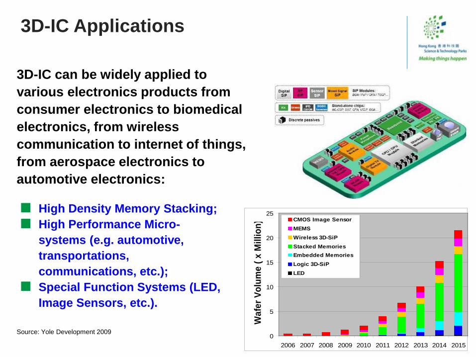
3D-IC Applications
3D-IC can be widely applied to various electronics products from consumer electronics to biomedical electronics, from wireless communication to internet of things, from aerospace electronics to automotive electronics:
0
5
10
15
20
25
2006 2007 2008 2009 2010 2011 2012 2013 2014 2015
Waf
er V
olum
e ( x
Mill
ion)
CMOS Image Sensor MEMS Wireless 3D-SiP Stacked Memories Embedded Memories Logic 3D-SiP LED
High Density Memory Stacking; High Performance Micro-systems (e.g. automotive, transportations, communications, etc.); Special Function Systems (LED, Image Sensors, etc.).
Source: Yole Development 2009

Moore’s Law
3
Source: http://www.hindawi.com/journals/acisc/2013/426962/fig15/
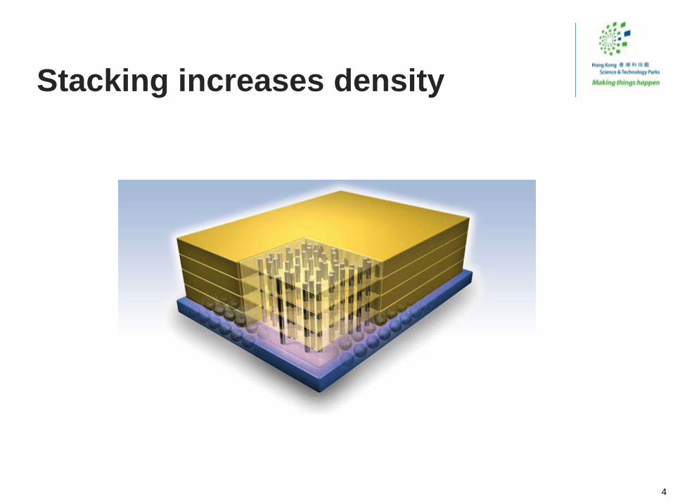
Stacking increases density
4
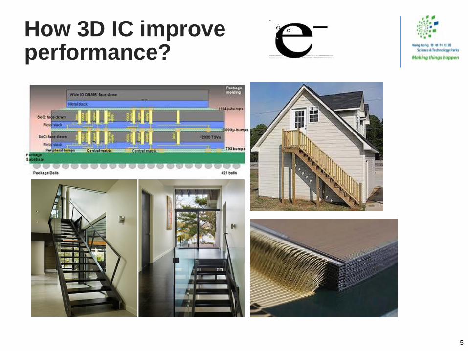
How 3D IC improve performance?
5
6
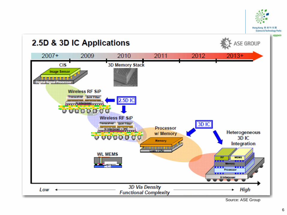
Source: ASE Group

HKSTPC 3D IC Services

IC Companies in Science Park
Over 80 companies of electronics cluster in Science Park

Expanding HKSTPC Lab Services
Green Tech Biotech Precision
Engineering IT/Telecom Electronics
Biotech Support Lab
Solar Energy Technical Support Centre
IC Design Centre
IP Servicing Centre
Probe & Test Centre
Failure Analysis Lab
Reliability Lab
Materials Analysis Lab
Wireless Communications
Test Lab
Solid State Lighting Lab
3D SiP Lab
3D WLP Lab
NEW !!!
All laboratories are within 15 minutes
walking distance in HKSP
> 500 manyears of experience!

Completing the IC Lab Services
Electronics
IC Design Centre
IP Servicing Centre
(by MPW)
Probe & Test Centre
Failure Analysis Lab
Reliability Lab
3D SiP & 3D WLP Lab
Packaging

2013/10/4
11
3D SiP Lab and Pilot Line (Phase 1)
Lead frame Packages. BGA on Organic Substrate Packages. MCM and COB on Laminate/Ceramics Substrate.
Die Attach (Placement 15μm @3sigma)
Plasma clean (Ar/N2 gas)
Wire bond (Placement 10μm @3sigma)
Transfer mold (Thermal set)
Liquid encapsulation
(High/ low viscosity)
T/F Press Trim & Singulation
(10 Tons Hydraulic)
Wafer Saw
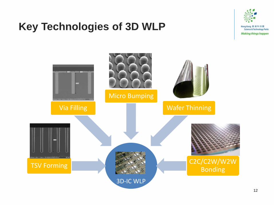
Key Technologies of 3D WLP
3D-IC WLP
TSV Forming
Via Filling
Micro Bumping
Wafer Thinning
C2C/C2W/W2W Bonding
12
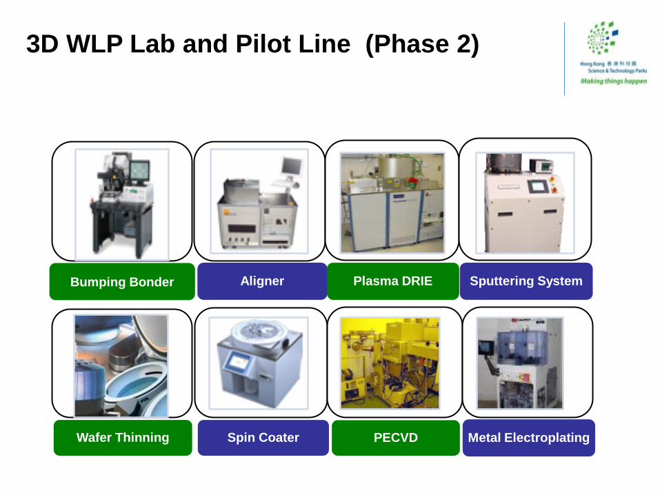
3D WLP Lab and Pilot Line (Phase 2)
Bumping Bonder
Wafer Thinning PECVD
Plasma DRIE Aligner
Spin Coater
Sputtering System
Metal Electroplating

National IC Design Base
Failure Analysis Thermal, stress,
molding, wiring failures
IC Design and IP Service EDA, Secure Virtual IP
Chamber
3D SiP / WLP Package Design
Package Design, CAD Tools
Reliability Test Qualification, Life
Testing
Wafer Testing Pilot Production
Test program development, wafer sort, final test
香港国家集成电路設計产业化基地

Design Testing Reliability Analysis
15
3D-IC Challenges

Hong Kong 3D-IC Capability
Source : ASTRI
Green Energy
Li-ion Battery Anode Materials CPV Module
Green Energy
Li-ion Battery Anode Materials CPV Module
LED
LED Chip, Packaging, Lighting & Control
Touch & Intelligent Display
3D Pico-projectors
SiP / 3D Packaging TPMS
Anti-counterfeit Identification
Printed Electronics
Healthcare Electronics
Optical Anti-shaking, Auto-focus & Zoom Camera Modules
Packaging & Sensing
SiP / 3D Packaging TPMS
Anti-counterfeit Identification
Printed Electronics
Healthcare Electronics
Optical Anti-shaking, Auto-focus & Zoom Camera Modules
Packaging & Sensing
3DIC Packaging &
Micro-fabrication
3DIC Packaging &
Micro-fabrication

3D SiP Lab Schedule
Approval Jun 2012 Move-in Apr 2013 Operation Commenced
2013/10/4
17

3D WLP Lab Schedule
Approval Mar 2013 Move-in Mar-Dec 2014 Operation Commence
Partial May 2014 Full Dec 2014
2013/10/4
18

Thank you!
19