3/4/5 cell battery protectors byd microelectronics … series datasheet wi-d06-j-0036 rev.a/1 2 /28...
TRANSCRIPT

BYD Microelectronics Co., Ltd.
BM3451 Series 3/4/5 Cell Battery Protectors
Datasheet WI-D06-J-0036 Rev.A/1 1 / 28
General Description The BM3451 is a professional protection IC for 3/4/5 cells rechargeable battery pack; it is highly
integrated, and generally used in power tools, electric bicycles and UPS applications. The BM3451 works constantly to monitor each cell’s voltage, the current of charge or discharge, and
the temperature of the environment to provide overcharge, over-discharge, discharge overcurrent, short circuit, charge overcurrent and over-temperature protections, etc. Besides, it also can change the protection delay time of overcharge, over-discharge and discharge overcurrent by setting the external capacitors.
The BM3451 provides external bleeding for cell-capacity balance function to avoid unbalanced capacity between each cell. Thus, the batteries can work for longer.
Extended function module embedded in the BM3451 ICs can make them work for more battery packs with multiple chips, and they can protect 6-cell batteries or more than 6-cell batteries.
Features (1) High-accuracy voltage detection for each cell ·overcharge threshold 3.6V~4.6V accuracy: ±25 mV (+25 )
accuracy: ±40 mV (-40 to +85) ·overcharge hysteresis 0.1V accuracy: ±50 mV ·over-discharge threshold 1.6V~3.0V accuracy: ±80 mV ·over-discharge hysteresis 0V / 0.2V / 0.4V accuracy: ±100 mV
(2) Three grades voltage detection of discharge overcurrent ·discharge overcurrent 1 0.025 V ~ 0.30 V (50 mV step) ·discharge overcurrent 2 0.2 V / 0.3V / 0.4V / 0.6 V ·short circuit 0.8V / 1.2 V
(3) Charge overcurrent detection ·detection voltage -0.03V / -0.05V / -0.1V / -0.15V / -0.2 V
(4) 3/4/5 cell protection enable (5) Setting of output delay time ·overcharge, over-discharge, discharge overcurrent 1 and discharge overcurrent 2 protection delay
time can be set by external capacitors (6) Supports external bleeding for balance (7) Controlling the state of charge or discharge by external signals (8) The maximum output voltage of CO / DO: 12V (9) Over-temperature protection (10) Breaking wire protection (11) Low power consumption ·operation mode(with Temp protection) 25 μA typical ·operation mode(without Temp protection) 15 μA typical ·sleeping mode 6 μA typical

BM3451 Series
Datasheet WI-D06-J-0036 Rev.A/1 2 /28
BYD Microelectronics Co., Ltd.
Applications ·Power tool ·Electric bicycle ·UPS backup battery
Packages ·TSSOP28 ·TSSOP20
Block Diagram
NTCTRH
VIN
TOVTOVDTOC1TOC2
BALUP
DOCO
DOINCOIN
BALDN
VM
Balance Control 2
Balance Control 1
CO DO Series
TEMP Protection
External DelayTime
Charger / Load
Detection
Logic Circuit
VC2
BAL2
VC4
BAL4
VC3
BAL3
VCC
BAL1
VC1
VC5
BAL5
GND
SET3/4/5 Cell selection
CO DO Driver OR
OCCT
OR
Dsicharge overcurrent Detection
Figure 1

BM3451 Series
Datasheet WI-D06-J-0036 Rev.A/1 3 /28
BYD Microelectronics Co., Ltd.
Selection Guides 1. Products name structure
Figure 2
2. Products catalogue
Type/Item
Overcharge
protection
voltage
[VDET1]
Overcharge
release
voltage
[VREL1]
Over-
discharge
protection
voltage
[VDET2]
Over-
discharge
release
voltage
[VREL2]
Discharge
overcurrent
1 detection
voltage
[VOC1]
Discharge
overcurrent
2 detection
voltage
[VOC2]
Short
circuit
detection
voltage
[VSHORT]
Charge
overcurrent
detection
voltage
[VOVCC]
Balance
detection
voltage
[VBAL]
BM3451VJDC-T28A 4.300V 4.200V 2.500V 2.700V 0.100V 0.400V 0.800V -0.100V 4.120V
BM3451SMDC-T28A 4.225V 4.125V 2.800V 3.000V 0.100V 0.400V 0.800V -0.100V 4.050V
BM3451HEDC-T28A 3.850V 3.750V 2.000V 2.500V 0.100V 0.400V 0.800V -0.100V 3.590V
BM3451VJDC-T20A 4.300V 4.200V 2.500V 2.700V 0.100V 0.400V 0.800V -0.100V -
BM3451SMDC-T20A 4.225V 4.125V 2.800V 3.000V 0.100V 0.400V 0.800V -0.100V -
BM3451HEDC-T20A 3.850V 3.750V 2.000V 2.500V 0.100V 0.400V 0.800V -0.100V -
Table 1
BM3451 Series
Datasheet WI-D06-J-0036 Rev.A/1 4 /28
BYD Microelectronics Co., Ltd.
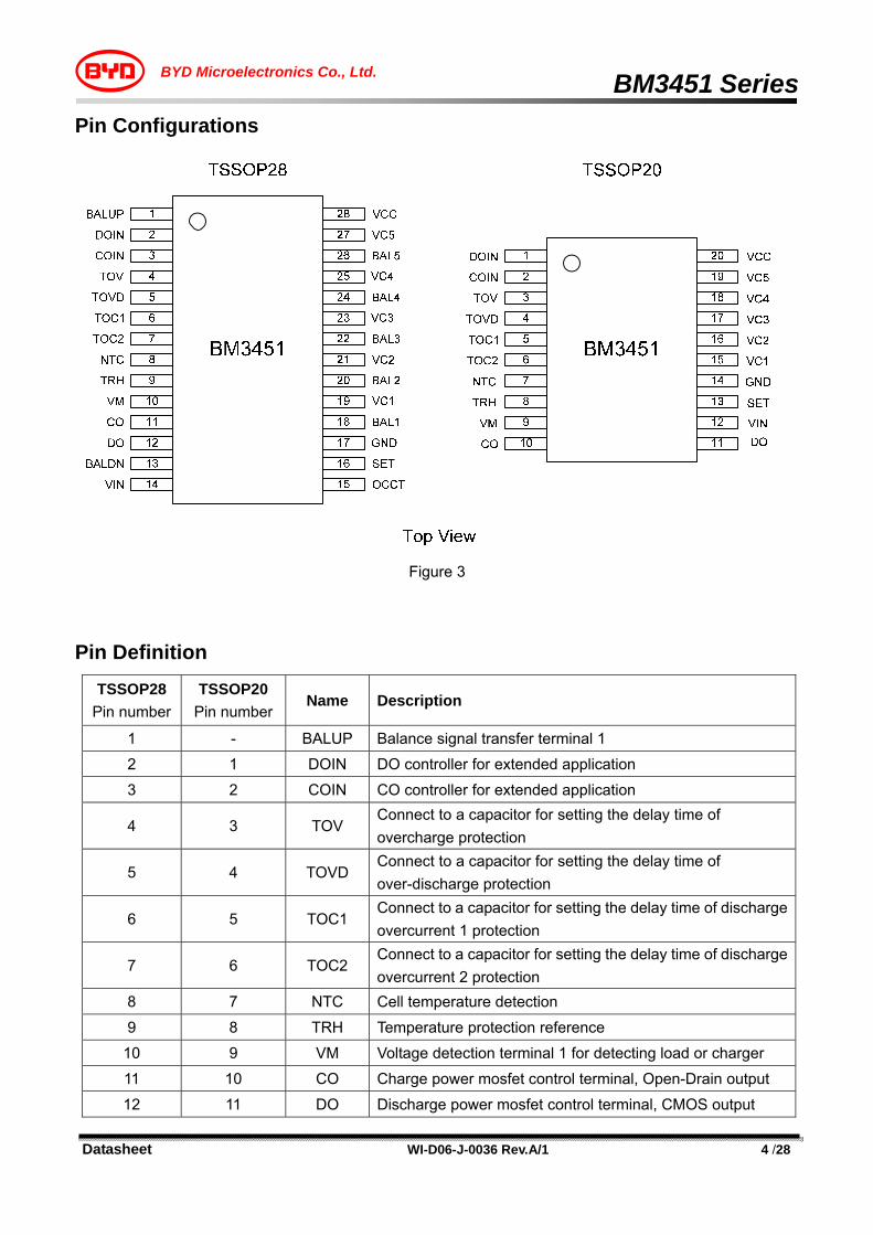
Pin Configurations
Figure 3
Pin Definition TSSOP28
Pin number TSSOP20
Pin number Name Description
1 - BALUP Balance signal transfer terminal 1 2 1 DOIN DO controller for extended application
3 2 COIN CO controller for extended application
4 3 TOV Connect to a capacitor for setting the delay time of overcharge protection
5 4 TOVD Connect to a capacitor for setting the delay time of over-discharge protection
6 5 TOC1 Connect to a capacitor for setting the delay time of discharge overcurrent 1 protection
7 6 TOC2 Connect to a capacitor for setting the delay time of discharge overcurrent 2 protection
8 7 NTC Cell temperature detection
9 8 TRH Temperature protection reference 10 9 VM Voltage detection terminal 1 for detecting load or charger
11 10 CO Charge power mosfet control terminal, Open-Drain output
12 11 DO Discharge power mosfet control terminal, CMOS output

BM3451 Series
Datasheet WI-D06-J-0036 Rev.A/1 5 /28
BYD Microelectronics Co., Ltd.
13 - BALDN Balance signal transfer terminal 2
14 12 VIN Charge and Discharge overcurrent Voltage detection terminal 2
15 - OCCT Discharge overcurrent release control terminal by load 16 13 SET Select terminal for 3/4/5 cell application
17 14 GND Ground pin of the IC, Cell1 negative input
18 - BAL1 Cell1 external bleeding control 19 15 VC1 Cell1 positive input, Cell2 negative input
20 - BAL2 Cell2 external bleeding control
21 16 VC2 Cell2 positive input, Cell3 negative input 22 - BAL3 Cell3 external bleeding control
23 17 VC3 Cell3 positive input, Cell4 negative input
24 - BAL4 Cell4 external bleeding control 25 18 VC4 Cell4 positive input, Cell5 negative input
26 - BAL5 Cell5 external bleeding control
27 19 VC5 Cell5 positive input 28 20 VCC Power supply,Cell5 positive input
Table 2
Absolute Maximum Ratings
Item Symbol Description Ratings Unit
Power supply voltage VCC - GND-0.3 ~ GND+30 V
Single cell input voltage VCELL Vcell5,Vcell4,Vcell3
Vcell2,Vcell1 GND-0.3 ~ GND+6 V
VM input voltage VM VM GND-20 ~ GND+30 V
DO output voltage VDO DO GND-0.3 ~ VCC+0.3 V
CO output voltage VCO CO GND-20 ~ VCC+0.3 V
Operating temperature TA - -40 ~ 85
Storage temperature TSTG - -40 ~ 125 Table 3
Caution: The absolute maximum ratings are rated values exceeding which the product could suffer
physical damage. These values must therefore not be exceeded in any conditions.

BM3451 Series
Datasheet WI-D06-J-0036 Rev.A/1 6 /28
BYD Microelectronics Co., Ltd.
Electrical Characteristics (TA=25 unless otherwise specified)
Item Symbol Test conditions*1 Min. Typ. Max. Unit Test
circuit
Power supply voltage VCC - 5 - 30 V 1 Operating consumption ICC V1=V2=V3=V4=V5=3.5V - - 25 μA
Sleeping consumption ISLP V1=V2=V3=V4=V5=2.0V - - 10 μA
Overcharge
Protection threshold
VDET1 V1=V2=V3=V4=3.5V
V5=3.5→4.4V VDET1
-0.025 VDET1
VDET1
+0.025 V
2
Protection delay time
TOV V1=V2=V3=V4=3.5V
COV=0.1μF V5=3.5V→4.4V0.5 1.0 1.5 s
Release threshold
VREL1 V1=V2=V3=V4=3.5V
V5=4.4V→3.5V VREL1
-0.05 VREL1
VREL1
+0.05 V
Release delay time
TREL1 V1=V2=V3=V4=3.5V
V5=4.4V→3.5V 10 20 30 ms
Temperature factor(1)
KU1 Ta= -40 to 85 -0.6 0 0.6 mV/
Over- discharge
Protection threshold
VDET2 V1=V2=V3=V4=3.5V
V5=3.5V→2.0V VDET2
-0.08 VDET2
VDET2
+0.08 V
Protection delay time
TOVD V1=V2=V3=V4=3.5V
COVD=0.1μF V5=3.5V→2.0V
0.5 1.0 1.5 s
Release threshold
VREL2 V1=V2=V3=V4=3.5V
V5=2.0V→3.5V VREL2
-0.10 VREL2
VREL2
+0.10 V
Release delay time
TREL2 V1=V2=V3=V4=3.5V
V5=2.0V→3.5V 10 20 30 ms
Discharge overcurrent
1
Protection threshold
VOC1 V1=V2=V3=V4=V5=3.5V
V6=0V→0.12V VOC1
*85% VOC1
VOC1
*115% V
3
Protection delay time
TOC1 V1=V2=V3=V4=V5=3.5V
COC1=0.1μF V6=0V→0.12V100 200 300 ms
Release delay time
TROC1 V1=V2=V3=V4=V5=3.5V
V6=0V→0.12V→0V 100 200 300 ms
Resistance between VM
and GND RVMS
V1=V2=V3=V4=V5=3.5V V6=0V→0.12V
100 300 500 kΩ
Temperature factor(2)
KU2 Ta= -40 to 85 -0.1 0 0.1 mV/
Discharge overcurrent
2
Protection threshold
VOC2 V1=V2=V3=V4=V5=3.5V
V6=0V→0.5V VOC2
*80% VOC2
VOC2
*120% V
Protection delay time
TOC2 V1=V2=V3=V4=V5=3.5V COC2=0.1μF V6=0V→0.5V
10 20 30 ms

BM3451 Series
Datasheet WI-D06-J-0036 Rev.A/1 7 /28
BYD Microelectronics Co., Ltd.
Short circuit
Protection threshold
VSHORT V1=V2=V3=V4=V5=3.5V
V6=0V→1.2V VSHORT
*80% VSHORT
VSHORT
*120% V
3 Protection delay time
TSHORT V1=V2=V3=V4=V5=3.5V
V6=0V→1.2V→0V 100 300 600 μs
Charge overcurrent
Protection threshold
VOVCC V1=V2=V3=V4=V5=3.5V
V6=0V→-0.2V VOVCC
-0.03 VOVCC
VOVCC
+0.03 V
4 Protection delay time
TOVCC V1=V2=V3=V4=V5=3.5V
V6=0V→-0.2V 10 20 30 ms
External bleeding voltage for balance
VBAL V1=V2=V3=V4=3.5V
V5=3.5V→4.30V VBAL
-0.05 VBAL
VBAL
+0.05 V 5
Output resistances
CO RCO Normal time, Co ”H” (12V) 3 5 8 kΩ 6
DO RDO Normal time, Do ”H” (12V) 3 5 8
kΩ 7 Protecting time, Do ”L” 0.20 0.35 0.50
BAL1 RBAL1 On ”H” 1.4 2.0 2.6
kΩ 8
Off ”L” 0.5 0.8 1.1
BAL2 RBAL2 On ”H” 1.4 2.0 2.6
Off ”L” 0.5 0.8 1.1
BAL3 RBAL3 On ”H” 1.4 2.0 2.6
Off ”L” 0.5 0.8 1.1
BAL4 RBAL4 On ”H” 1.4 2.0 2.6
Off ”L” 0.5 0.8 1.1
BAL5 RBAL5 On ”H” 1.4 2.0 2.6
Off ”L” 0.5 0.8 1.5
Table 4 *1: All the test condition parameters above are designed based on Li+ parameters, other grade parameters can adjust by their own actual voltages.

BM3451 Series
Datasheet WI-D06-J-0036 Rev.A/1 8 /28
BYD Microelectronics Co., Ltd.
Function Description 1. Overcharge
During charging, VIN >VOVCC when IC doesn’t work in the state of charge overcurrent, If any of VC1, (VC2-VC1), (VC3-VC2), (VC4-VC3) and (VC5-VC4) is higher than VDET1 and lasts longer than TOV,
BM3451 chip considers that the batteries work in the state of overcharge, the output voltage of CO will become to high resistance from high level, and then it will be pulled down to low level by external resistor. The charge MOSFET will be turned off and stop charging.
The overcharge protection state will be released if any of the next conditions occurs: (1) All cells’ voltage is less than the Overcharge release threshold VREL1 and stays a period of time
TREL1. (2) VM> 100mV (connecting to the load), Battery voltage is lower than VDET1 and stays a period of time
TREL1.
2. Over-discharge During discharging, VIN<VOVCC when IC doesn’t work in the state of discharge overcurrent. If any of
VC1, (VC2-VC1), (VC3-VC2), (VC4-VC3) and (VC5-VC4) is less than VDET2 and lasts longer than TOVD. BM3451 chip considers that the batteries work in the state of over-discharge and the output voltage of DO will turn to GND. The discharge MOSFET will be turned off and stop discharging, then the chip will enter sleeping mode.
The over-discharge protection state will be released if any of the next conditions occurs: (1) VM =0mV, all cells’ voltage is higher than VREL2 and stays a period of time TREL2. (2) VM <-100mV (connecting to the charger), all cells’ voltage is higher than VDET2 and stays a period of
time TREL2.
3. Discharge Overcurrent During discharging, the current varies with the load. The voltage of VIN becomes higher with the current
increasing. When the voltage of VIN is higher than VOC1 and stays longer than TOC1, we think the IC works in the state of discharge overcurrent 1; When the voltage of VIN is higher than VOC2 and stays longer than TOC2, we consider the IC works in the state of discharge overcurrent 2; When the voltage of VIN is higher than VSHORT and stays longer than TSHORT, we think the IC works in the state of short circuit. When any of the three states occurs, the output voltage of DO changes to low level to turn off the discharge MOSFET and stop discharging. At the same time, RVMS which is the inner pulling down resistance of VM is connected, and we know that VM is pad which we can lock the output voltage of DO by when chip works in the state of over-current discharge. Usually VOC1 < VOC2 < VSHORT, TOC1 > TOC2 > TSHORT .When IC works in discharge overcurrent, the output voltage of DO is locked in low level. The discharge overcurrent protection state will be released when disconnect the load.
4. Delay Time Setting
Overcharge and Over-discharge delay time can be calculated as follow: Tov = 107 x COV; Tovd = 107 x COVD Discharge overcurrent 1 delay time can be calculated as follow: Toc1 = 2 x 10⁶ x COC1 Discharge overcurrent 2 delay time can be calculated as follow: Toc2 = 2 x 10⁵ x COC2

BM3451 Series
Datasheet WI-D06-J-0036 Rev.A/1 9 /28
BYD Microelectronics Co., Ltd.
5. Charge Overcurrent During charging, if the current is biggish with VIN<VOVCC and stays longer than TOVCC, the BM3451 chip
considers that the batteries work in the state of charge overcurrent, the output voltage of CO will be pulled down to low level and the charge MOSFET will be turned off and stop charging. Charge overcurrent protection will be released when we disconnect the charger.
6. Balance Function
Cells’ balance function is used to balance the cells’ capacity in a pack. When all voltages of VC1, (VC2-VC1), (VC3-VC2), (VC4-VC3) and (VC5-VC4) are lower or higher than VBAL , all the external balance discharge circuits will not work. Otherwise the cell, whose voltage is higher than VBAL, will turn on the external discharge circuit and make its voltage lower than VBAL. During charging, If the highest voltage of five cells enters overcharge state and its cell balance circuit turns on, the charge control MOSFET turns off and the external discharge circuit works and makes the battery voltage fall down to VREL1 which is the overcharge release threshold, then turn on the charge control MOSFET for continuing charge .For a long enough time of charge and discharge cycles, the voltages of all cells will reach to more than VBAL, and avoid the capacity differences between batteries. 7. Over-temperature
Usually, batteries should be prevented charging and discharging from over-temperature. The BM3451 chip has this over-temperature protection. The thermostat resistor connecting to NTC pad is used to induct the pack’s temperature, the resistor connecting TRH pad is used to set the reference of over-temperature protection. Assuming the resistance of NTC is RNTC when the pack gets to the temperature of charge over-temperature protection, and then we set the resistance RTRH of TRH be RTRH =2* RNTC. The over-discharge protection temperature is the temperature when the resistance of NTC become to 0.54* RNTC. We can set the temperature of charge and discharge protection by changing the value of RTRH.
Take 103AT-4 for example, NTC resistance is 10KΩ in normal temperature (25 ), and the temperature
of charge over-temperature protection is 55.When the temperature is 55 and chip works in the state of charging, RNTC is 3.5KΩ, so RTRH is equal to 7KΩ. We also know the NTC resistance is 0.54*RNTC=1.89 KΩ when the pack arrive to the temperature of discharge over-temperature, the temperature is 75 in this condition. The hysteresial temperature of charge over-temperature is 5 and the hysteresial temperature of discharge over-temperature is 15. During charging, when the temperature is higher than 55, the output voltage of CO turns to high resistance, and will be pulled down to low level by external resistor, charge control MOSFET will be turned off and stops charging. And when the pack’s temperature falls down to 50, CO changes to high level and charge control MOSFET be turned on again. During discharging, when the temperature is higher than 75, the output voltage of DO becomes to low level, discharge control MOSFET will be turned off and stop discharging, at the same time charge control MOSFET will also be turned off and stops charging. When pack’s temperature falls down to 60, the output of CO and DO turn to high level, charge and discharge control MOSFET will both be turned on again. 8. Breaking wire protection
When one or multi wires of VC1, VC2, VC3, VC4 and VC5 are detected cut from the batteries by the BM3451 chip, the IC will consider it enters a state of breaking wire, then CO will be in high resistance and DO will turn to GND level, then the IC enters low consumption state.
When the breaking wires are connected correctly again, the IC will exit breaking wire protection. Specially attention, regardless one chip application or multi-chip application, the GND pin must not be open from the battery, or the IC cannot operate normally, and it cannot protect correctly.

BM3451 Series
Datasheet WI-D06-J-0036 Rev.A/1 10 /28
BYD Microelectronics Co., Ltd.
9. 3/4/5 cells application selection SET voltage Cells Short pins
Floating 5 - VCC 4 VC1=GND GND 3 VC1=VC2=GND
Chart 5 10. Extended application
When the BM3451 chip is used in extended condition, each IC transfers its information of overcharge, over-discharge, and balance to neighboring ICs. Take application of figure 6 for example, the information of DO and CO of IC1 will transfer to DOIN and COIN of IC2, then IC2 control external MOSFETs turn on or turn off by the voltage of DOIN and COIN. DOIN and COIN have precedence to control DO and CO over internal protection signals. Balance information transfer by BALUP and BALDN, IC follows the rule that inner balance has precedence over external balance.
Take extended application of three ICs with A, B, C for example, the external rule of balance is as follows:
A B C Balance of A (ON or OFF)
Balance of B (ON or OFF)
Balance of C (ON or OFF)
0 0 0 OFF OFF OFF 0 0 1 OFF OFF ON 0 1 0 OFF ON OFF 0 1 1 OFF ON ON 1 0 0 ON OFF OFF 1 0 1 ON OFF ON 1 1 0 ON ON OFF 1 1 1 OFF OFF OFF
Signal descriptions: “1” shows that any of the batteries is equal to or above VBAL, “0” shows that at least
one of the batteries is lower than VBAL.
BM3451 Series
Datasheet WI-D06-J-0036 Rev.A/1 11 /28
BYD Microelectronics Co., Ltd.
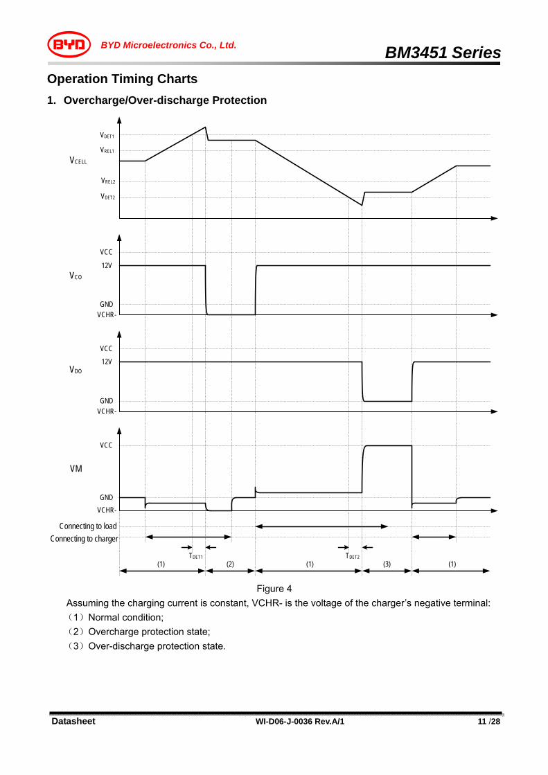
Operation Timing Charts 1. Overcharge/Over-discharge Protection
VDET1
VREL2
VDET2
VREL1
VCC
GND
VCC
VCHR-GND
VCC
GND
(1) (1)(3)(1)(2)
VCELL
VCO
VM
VDO
TDET1 TDET2
Connecting to chargerConnecting to load
VCHR-
VCHR-
12V
12V
Figure 4 Assuming the charging current is constant, VCHR- is the voltage of the charger’s negative terminal: (1)Normal condition; (2)Overcharge protection state; (3)Over-discharge protection state.

BM3451 Series
Datasheet WI-D06-J-0036 Rev.A/1 12 /28
BYD Microelectronics Co., Ltd.
2. Discharge Overcurrent / Short Circuit / Charge Overcurrent Protection
VDET1
VREL2
VDET2
VREL1
VCC
GND
VCC
VCHR-
GND
VCC
GND
(1) (1)(4)(1)(2)
VCELL
VCO
VM
VDO
TOC1 TSHORT
Connecting to chargerConnecting to load
VCHR-
VCHR-
VCC
GND
VIN
VCHR-
12V
12V
VOC1
VOVCC
VSHORT
VOC2
TOC2 TOVCC(3) (1) (5) (1)
Figure 5
Assuming the charging current is constant, VCHR- is the voltage of the charger’s negative terminal: (1) Normal condition; (2) Discharge overcurrent 1 protection state; (3) Discharge overcurrent 2 protection state; (4) Short circuit protection state; (5) Charge overcurrent protection state.
BM3451 Series
Datasheet WI-D06-J-0036 Rev.A/1 13 /28
BYD Microelectronics Co., Ltd.
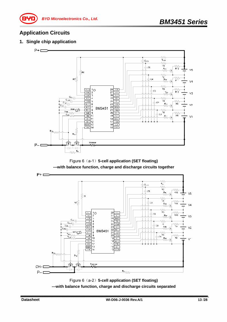
Application Circuits 1. Single chip application
Figure 6(a-1)5-cell application (SET floating) ---with balance function, charge and discharge circuits together
Figure 6(a-2)5-cell application (SET floating)
---with balance function, charge and discharge circuits separated

BM3451 Series
Datasheet WI-D06-J-0036 Rev.A/1 14 /28
BYD Microelectronics Co., Ltd.
Figure 6(b)4-cell application (SET be connected to VCC) ---with balance function
Figure 6(c)3-cell application (SET be connected to GND)---with balance function

BM3451 Series
Datasheet WI-D06-J-0036 Rev.A/1 15 /28
BYD Microelectronics Co., Ltd.
Figure 6(d-1)5-cell application (SET floating)
---without balance function, charge and discharge circuits together
Figure 6(d-2)5-cell application (SET floating)
---without balance function, charge and discharge circuits separated
BM3451 Series
Datasheet WI-D06-J-0036 Rev.A/1 16 /28
BYD Microelectronics Co., Ltd.
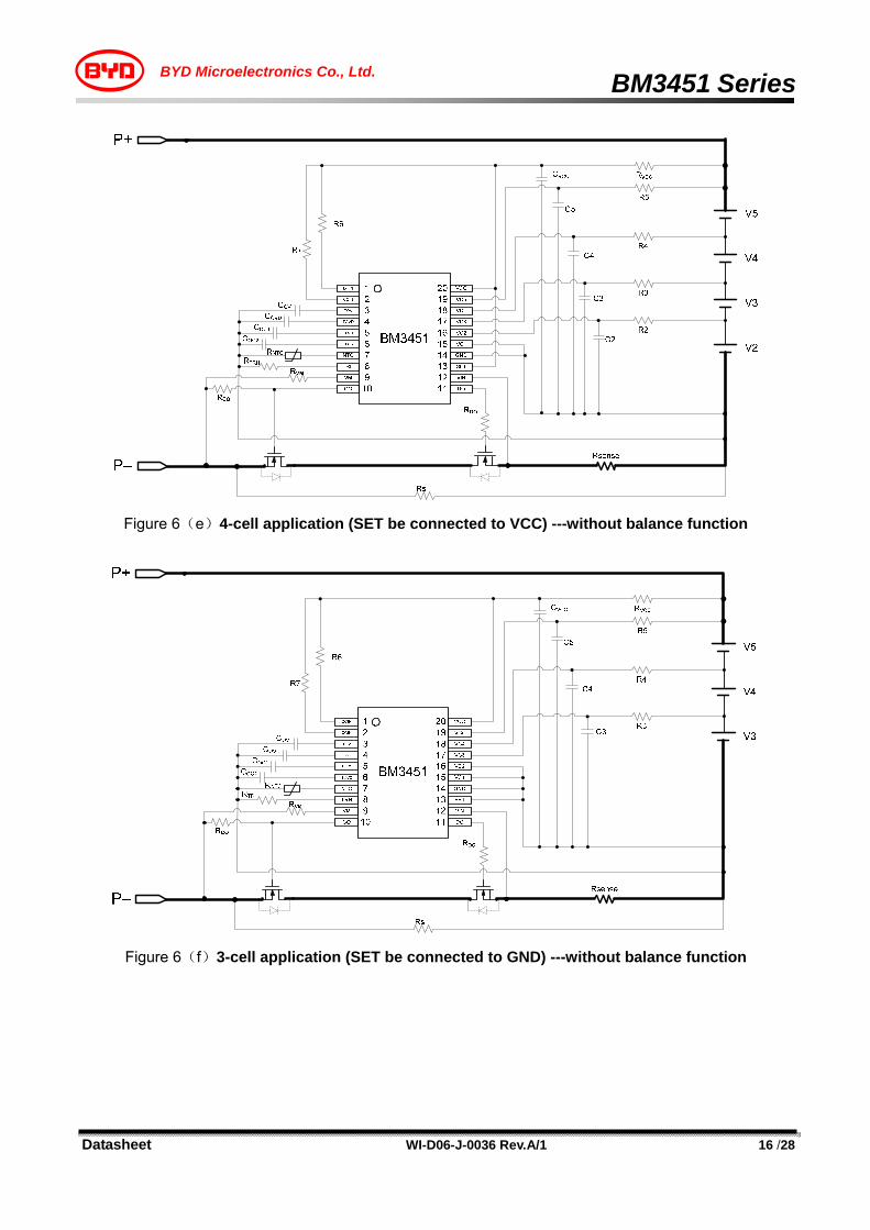
Figure 6(e)4-cell application (SET be connected to VCC) ---without balance function
Figure 6(f)3-cell application (SET be connected to GND) ---without balance function

BM3451 Series
Datasheet WI-D06-J-0036 Rev.A/1 17 /28
BYD Microelectronics Co., Ltd.
Constants for External Components: Component Symbol Typ. Range Unit R1, R2, R3, R4, R5 1000 100 ~ 1000 Ω
RB1, RB2, RB3, RB4, RB5 4.7 3~10 MΩ RVCC 1000 100 ~ 1000 Ω
R6, R7 1 1 ~ 2 MΩ R8, R9, R10, R11, R12 47 10 ~ 200 Ω
RNTC 10 - kΩ RTRH 7 - kΩ RVM 220 10-500 kΩ
RCO, RS 10 5~15 MΩ RDO 2 1~10 kΩ
Rsense 5 1 ~ 20 mΩ CVCC 10 10 ~ 100 μF
C1, C2, C3, C4, C5 1.0 0.1 ~ 10 Maximum endurable
voltage >50V
μF
COV, COVD, COC1, COC2 0.1
- μF
Table 6

BM3451 Series
Datasheet WI-D06-J-0036 Rev.A/1 18 /28
BYD Microelectronics Co., Ltd.
2. Two chips extended application
R20
R19
R18
R17
R16R6
R7
R8
R9
R10
RVCC2
C6
R24
R23
COV2
P+
V6
V10
V9
V8
V7
C10
C9
C8
C7
CVCC2
COVD2
R15
R14
R13
R12
R11R1
R2
R3
R4
R5
RVCC1
C1
R22
R21
COV1
RTRH
Rsense
V1
V5
V4
V3
V2
C5
C4
C3
C2
CVCC1
COC2
COC1
COVD1
P–
D1
M1 RVM
RCO
1
BM34516
1413121110987
5432
28
23
1516171819202122
24252627
BALUP
DOIN
COIN
TOV
TOVD
TOC1
TOC2
NTC
TRH
VM
CO
DO
BALDN
VIN OCCT
SET
GND
BAL1
VC1
BAL2
VC2
BAL3
VC3
BAL4
VC4
BAL5
VC5
VCC
1
BM34516
1413121110987
5432
28
23
1516171819202122
24252627
BALUP
DOIN
COIN
TOV
TOVD
TOC1
TOC2
NTC
TRH
VM
CO
DO
BALDN
VIN OCCT
SET
GND
BAL1
VC1
BAL2
VC2
BAL3
VC3
BAL4
VC4
BAL5
VC5
VCC
R25
P1
RDO
RNTC
RS
CCOIN
CDOIN
RB1
RB2
RB3
RB4
RB5
RB6
RB7
RB8
RB9
RB10
Rp
D2
Figure 7 10-cell application——with balance function

BM3451 Series
Datasheet WI-D06-J-0036 Rev.A/1 19 /28
BYD Microelectronics Co., Ltd.
R6
R7
R8
R9
R10
RVCC2
C6
R24
R23
COV2
P+
V6
V10
V9
V8
V7
C10
C9
C8
C7
CVCC2
COVD2
R1
R2
R3
R4
R5
RVCC1
C1
R22 R21
COV1
Rsense
C5
C4
C3
C2
CVCC1
COC2
COC1
COVD1
P–
D1
M1RVM
RCO
R25
P1
RDO
RS
CCOINCDOIN
Rp
D2
1DOIN
BM3451
COIN
TOC1
TOC2
TOV
TOVD
NTC
TRH
VM
CO
6
10987
5432
20 VCC
VC5
VC2
VC1
VC4
VC3
GND
SET
VIN
DO
15
11121314
16171819
V1
V5
V4
V3
V2
1DOIN
BM3451
COIN
TOC1
TOC2
TOV
TOVD
NTC
TRH
VM
CO
6
10987
5432
20 VCC
VC5
VC2
VC1
VC4
VC3
GND
SET
VIN
DO
15
11121314
16171819
RTRH
RNTC
Figure 8 10-cell application——without balance function
Caution:The maximum endurable voltage of the MOS M1, the diode D1, D2 and the transistor P1 must
be more than the total voltage of the whole battery packages, and keep enough voltage room. Above of 4-cell, 3-cell, and 10cell applications are charge and discharge circuits together, charge and discharge separated circuits can refer to 5-cell application.

BM3451 Series
Datasheet WI-D06-J-0036 Rev.A/1 20 /28
BYD Microelectronics Co., Ltd.
Constants for External Components: Component Symbol Typ. Range Unit R1, R2, R3,R4, R5, R6,R7, R8, R9, R10
1000 100 ~ 1000 Ω
RB1, RB2, RB3, RB4, RB5, RB6, RB7, RB8, RB9, RB10
4.7 3 ~ 10 MΩ
RVCC1, RVCC2 1000 100 ~ 1000 Ω R11, R12,R13, R14, R15, R16, R17, R18, R19, R20
47 10 ~ 200 Ω
R21, R22, R25 10 8 ~ 15 MΩ R23, R24, RP 1 1 ~ 2 MΩ RNTC1, RNTC2 10 - kΩ RTRH1,RTRH2 7 - kΩ
RVM 200 10-500 kΩ RCO, RS 10 5~15 MΩ
RDO 2 0~10 kΩ Rsense 5 0.1 ~ 20 mΩ
CVCC1, CVCC2 10 10 ~ 100
Maximum endurable
voltage >50V
μF C1, C2, C3, C4, C5, C6, C7, C8, C9, C10
0.1 0 ~ 0.33 μF
COV1, COVD1, COV2, COVD2, COC1, COC2
0.1 - μF
CDOIN, CCOIN 33 33~100 nF Table 7

BM3451 Series
Datasheet WI-D06-J-0036 Rev.A/1 21 /28
BYD Microelectronics Co., Ltd.
Test Circuits The next tests take 5-cell application for example, so that SET pin is floating. If 4-cell application is selected, we set SET pin to VCC level and force GND voltage level to VC1; else if 3-cell application is selected, we set SET pin to GND level and force GND voltage level to VC1 and VC2. The test methods of 4-cell and 3-cell application are as same as 5-cell application. 1. Normal and Sleeping Current Consumption
Test circuit 1 (1) Set V1=V2=V3=V4=V5=3.50V, the current flowing to GND is the normal operating current
consumption. (2) On the condition of (1), then set V1=V2=V3=V4=V5=2.0V, the current flowing to GND is the
sleeping current consumption.
2. Overcharge Protection Test Test circuit 2 2.1 Overcharge threshold (VDET1) and Overcharge release threshold (VREL1)
Set V1=V2=V3=V4=V5=3.50V, make sure the output voltages of DO and CO pins are “H” level. Increase V5 gradually, monitor CO voltage and keep the condition not shorter than Tdet1, the value of V5 when CO turns from “H” to “L” is the overcharge threshold voltage. Decrease V5, the V5 when CO returns to “H” level again is the overcharge release threshold.
2.2 Overcharge protection delay time and Overcharge release delay time (1) Set V1=V2=V3=V4=V5=3.50V, make sure the output voltages of DO and CO pins are “H” level.
Increase V5 to 4.4V from 3.5V instantaneously, monitor CO voltage and keep a period of time. The time interval when CO turns from “H” to “L” is the overcharge protection delay time.
(2) Set V1=V2=V3=V4=3.50V, V5=4.4V, make sure the output voltage of DO is “H” level, CO is “L” level. Decrease V5 to 3.5V from 4.4V instantaneously, monitor CO voltage and keep a period of time. The time interval when the output voltage of CO turns from “L” to “H” is the overcharge release delay time.
3. Over-discharge Protection Test Test circuit 2 3.1 Over-discharge threshold (VDET2) and Over-discharge release threshold (VREL2)
Set V1=V2=V3=V4=V5=3.50V, make sure the output voltages of DO and CO pins are “H” level. Decrease V5 gradually, monitor DO voltage and keep the condition not shorter than Tdet2, the value of V5 when the output voltage of DO turns from “H” to “L” is the over-discharge threshold voltage. Increase V5, the value of V5 when DO returns to “H” level again is the over-discharge release threshold.
3.2 Over-discharge protection delay time and Over-discharge release delay time (1) Set V1=V2=V3=V4=V5=3.50V, make sure the output voltages of DO and CO pins are “H” level.
Decrease V5 to 2.0V instantaneously, monitor DO voltage and keep a period of time. The time interval when DO turns from “H” to “L” is the over-discharge protection delay time.
(2) Set V1=V2=V3=V4=3.50V, V5=2.0V, make sure CO is “H” level, DO is “L” level. Increase V5 to 3.5V instantaneously, monitor DO voltage and keep a period of time. The time interval when the output voltage of DO turns from “L” to “H” is the overcharge release delay time.

BM3451 Series
Datasheet WI-D06-J-0036 Rev.A/1 22 /28
BYD Microelectronics Co., Ltd.
4. Discharge overcurrent and short circuit Protection Test Test circuit 3 4.1 Discharge overcurrent1 and 2 threshold (VDET3, VDET4) and short circuit threshold (VSHORT)
Set V1=V2=V3=V4=V5=3.5V, V6=0V, make sure the output voltages of DO and CO pins are “H” level. Increase V6 gradually, monitor Do voltage and keep the condition for a period of time, the value of V6 when the output voltage of Do turns from “H” to “L”, is the discharge overcurrent 1 threshold (VDET3). Decrease V6, the discharge overcurrent 1 protection will be released. VDET4 and VSHORT can also be tested by their protection time differences, but V6 has a larger change.
4.2 Discharge overcurrent protection delay time and release delay time (1) Set V1=V2=V3=V4=V5=3.50V, V6=0V, make sure the output voltages of DO and CO pins are “H”.
Increase V6 to 0.2V instantaneously, monitor DO voltage and keep a period of time. The time interval when the output voltage of DO turns from “H” to “L” is the discharge overcurrent 1 protection delay time.
(2) Set V1=V2=V3=V4=V5=3.50V, V6=0V, make sure the output voltages of DO and CO pins are “H”. Increase V6 instantaneously with its value be larger, monitor DO voltage and keep a period of time. The time interval when the output voltage of DO turns from “H” to “L” is the discharge overcurrent 2 protection delay time, make sure its value is less than the discharge overcurrent 1 protection delay time, then the value of V6 at this time is the discharge overcurrent 2 threshold.
(3) Set V1=V2=V3=V4=V5=3.50V, V6=0V, make sure the voltages of DO and CO pins are “H”. Increase V6 instantaneously with its value lager and larger, monitor DO voltage and keep a period of time. The time interval when DO turns from “H” to “L” is the short circuit protection delay time, make sure its value is less than the discharge overcurrent 2 protection delay time, and the value of V6 at this time is the short circuit threshold.
(4) Set V1=V2=V3=V4=V5=3.50V, V6=0.2V, make sure the output voltage of DO pin and CO pin is “L” and “H”. Decrease V6 to 0V instantaneously, monitor DO voltage and last a period of time. The time interval when DO turns from “L” to “H” is the discharge overcurrent 1 release delay time, we can test the release delay time of discharge overcurrent 2 and short circuit by using the same method.
5. Charge overcurrent Protection Test Test circuit 4 5.1 Charge overcurrent threshold
Set V1=V2=V3=V4=V5=3.50V, V7=0V, make sure the output voltages of DO and CO pins are “H”. Increase V6 gradually, monitor CO voltage and keep a period of time. The value of V7 when the output voltage of CO turns from “H” to “L” is the charge overcurrent threshold.
5.2 Charge overcurrent protection delay time Set V1=V2=V3=V4=V5=3.50V, V7=0V, make sure the output voltages of DO and CO pins are “H”. Increase V7 to 0.3V instantaneously, monitor the CO voltage and keep a period of time. The time interval when the output voltage of CO pin turns from “H” to “L” is the charge overcurrent protection delay time.
6. Cell Balance threshold Test
Test circuit 5 Set V1=V2=V3=V4=V5=3.50V, make sure the output voltage of BAL1 pin is 0V. Increase V1

BM3451 Series
Datasheet WI-D06-J-0036 Rev.A/1 23 /28
BYD Microelectronics Co., Ltd.
gradually and monitor the voltage of BAL1. The value of V1 when the output voltage of BAL1 pin turns from “0” to “H” (the voltage of V1) is the cell balance threshold. The test method of other cells balance is as same as the method of V1.
7. Output/Input Resistance Test 7.1 The output resistances of CO and DO (1) The output resistance when the output voltages of CO and DO pins are both “H”.
Test circuit 6 Set V1=V2=V3=V4=V5=3.50V, V6=12.0V, turn off the switch K and make sure the output voltage of CO pin is “H”. Measure the voltage VA of CO pin; turn on the switch K, decrease the voltage V6 gradually from 12V, monitor the value of IA, and note down the output voltage VB of CO pin when the value of IA is 50uA, then the output resistance of CO is calculated as follows: RCOH = (VA - VB)/50 (MΩ) We can also test the output resistance RDOH of DO pin with using the same method.
(2) The output resistance when the output voltage of DO pin is “L”. Test circuit 7 Set V1=V2=V3=V4=V5=2.00V, V8=0.00V, turn off the switch K and make sure the output voltage of DO pin is “L”. Turn on the switch K, increase the voltage V8 gradually from 0V, monitor the value of IA, note down the output voltage VDO of DO pin when the value of IA is 50uA, then the output resistance of DO is calculated as follows: RDOL= VDO/50 (MΩ)
7.2 The output resistances of balance pins BAL1, BAL2, BAL3, BAL4, BAL5 Test circuit 8
(1) Set VBAL < V1 < VDET1, V2=V3=V4=V5=3.5V, turn on the switch K1 and turn off K2, K3, K4, K5,decrease V9 from VBAL ,note down the value V_9, which is the value of V9 when the current is 50uA, then the output resistance when the cell balance turn on is calculated as follows: RBAL1H=(V1-V_9)/50 (MΩ);
(2) Set V1=V2=V3=V4=V5=3.50V, turn on the switch K1 and turn off K2, K3, K4, K5, increase V9 from 0V ,note down the value V_9, which is the value of V9 when the current is -50uA, then the output resistance when the cell balance turn off is calculated as follows: RBAL1L=V_9/50 (MΩ);
(3) Set VBAL < V2 < VDET1, V1=V3=V4=V5=3.5V, turn on the switch K2 and turn off K1, K3, K4, K5,decrease V9 from (V1+VBAL) ,note down the value V_9, which is the value of V9 when the current is 50uA, then the output resistance when the cell balance turn on is calculated as follows: RBAL2H=(V1+V2-V_9)/50 (MΩ);
(4) Set V1=V2=V3=V4=V5=3.50V, turn on the switch K2 and turn off K1, K3, K4, K5, increase V9 from V1 ,note down the value V_9, which is the value of V9 when the current is -50uA, then the output resistance when the cell balance turn off is calculated as follows: RBAL1L=(V_9-V1)/50 (MΩ);
(5) Set VBAL < V3 < VDET1, V1=V2=V4=V5=3.5V, turn on the switch K3 and turn off K1, K2, K4, K5,decrease V9 from (V1+V2+VBAL) ,note down the value V_9, which is the value of V9 when the current is 50uA, then the output resistance when the cell balance turn on is calculated as follows: RBAL2H=(V1+V2+V3-V_9)/50 (MΩ);
(6) Set V1=V2=V3=V4=V5=3.50V, turn on the switch K3 and turn off K1, K2, K4, K5, increase V9 from (V1 +V2),note down the value V_9, which is the value of V9 when the current is -50uA, then the output resistance when the cell balance turn off is calculated as follows: RBAL1L=(V_9-V1-V2)/50 (MΩ);
BM3451 Series
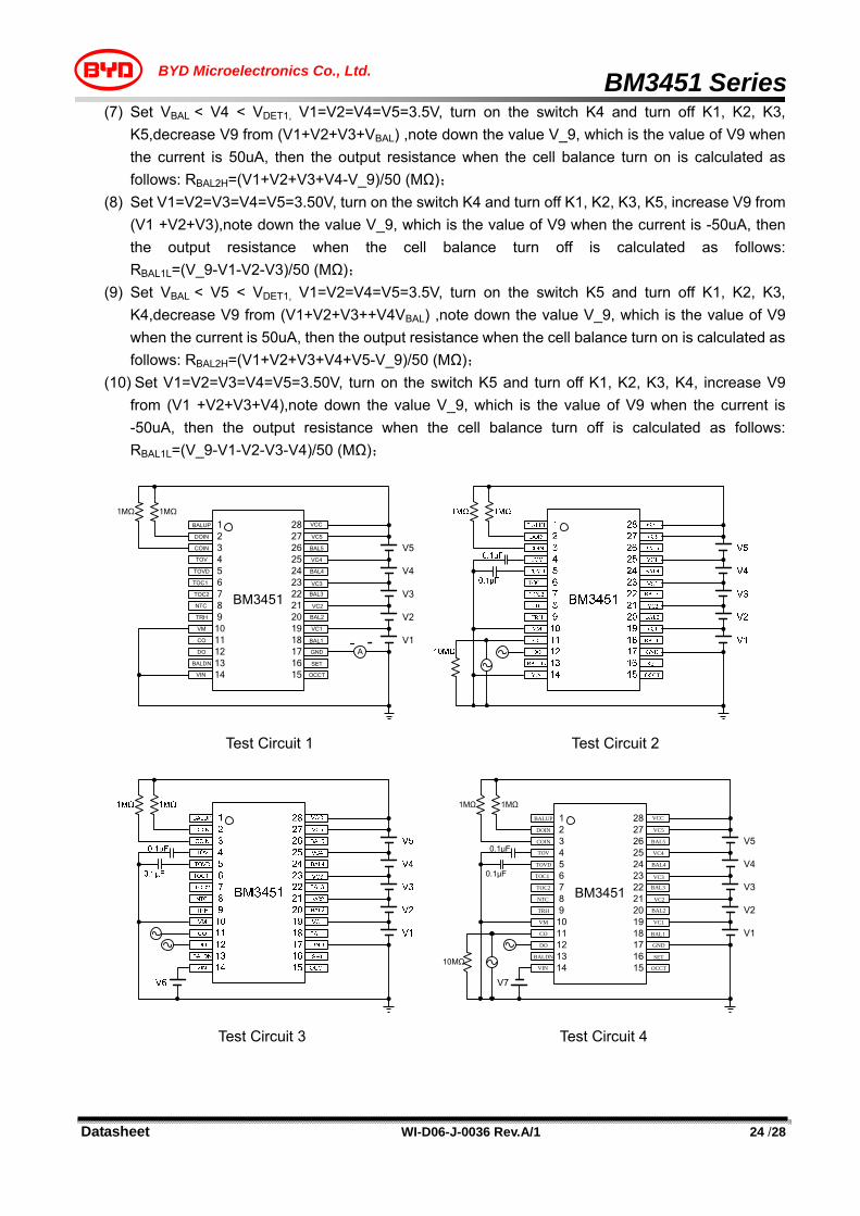
Datasheet WI-D06-J-0036 Rev.A/1 24 /28
BYD Microelectronics Co., Ltd.
(7) Set VBAL < V4 < VDET1, V1=V2=V4=V5=3.5V, turn on the switch K4 and turn off K1, K2, K3, K5,decrease V9 from (V1+V2+V3+VBAL) ,note down the value V_9, which is the value of V9 when the current is 50uA, then the output resistance when the cell balance turn on is calculated as follows: RBAL2H=(V1+V2+V3+V4-V_9)/50 (MΩ);
(8) Set V1=V2=V3=V4=V5=3.50V, turn on the switch K4 and turn off K1, K2, K3, K5, increase V9 from (V1 +V2+V3),note down the value V_9, which is the value of V9 when the current is -50uA, then the output resistance when the cell balance turn off is calculated as follows: RBAL1L=(V_9-V1-V2-V3)/50 (MΩ);
(9) Set VBAL < V5 < VDET1, V1=V2=V4=V5=3.5V, turn on the switch K5 and turn off K1, K2, K3, K4,decrease V9 from (V1+V2+V3++V4VBAL) ,note down the value V_9, which is the value of V9 when the current is 50uA, then the output resistance when the cell balance turn on is calculated as follows: RBAL2H=(V1+V2+V3+V4+V5-V_9)/50 (MΩ);
(10) Set V1=V2=V3=V4=V5=3.50V, turn on the switch K5 and turn off K1, K2, K3, K4, increase V9 from (V1 +V2+V3+V4),note down the value V_9, which is the value of V9 when the current is -50uA, then the output resistance when the cell balance turn off is calculated as follows: RBAL1L=(V_9-V1-V2-V3-V4)/50 (MΩ);
V1
V5
V4
V3
V2
1MΩ 1MΩ
A
1
BM34516
1413121110987
5432
28
23
1516171819202122
24252627
BALUP
DOIN
COIN
TOV
TOVD
TOC1
TOC2
NTC
TRH
VM
CO
DO
BALDN
VIN OCCT
SET
GND
BAL1
VC1
BAL2
VC2
BAL3
VC3
BAL4
VC4
BAL5
VC5
VCC
-
Test Circuit 1 Test Circuit 2
V1
V5
V4
V3
V2
1MΩ 1MΩ
0.1μF
0.1μF
V7
1
BM34516
1413121110987
5432
28
23
1516171819202122
24252627
BALUP
DOIN
COIN
TOV
TOVD
TOC1
TOC2
NTC
TRH
VM
CO
DO
BALDN
VIN OCCT
SET
GND
BAL1
VC1
BAL2
VC2
BAL3
VC3
BAL4
VC4
BAL5
VC5
VCC
10MΩ
Test Circuit 3 Test Circuit 4

BM3451 Series
Datasheet WI-D06-J-0036 Rev.A/1 25 /28
BYD Microelectronics Co., Ltd.
Test Circuit 5 Test Circuit 6
Test Circuit 7 Test Circuit 8

BM3451 Series
Datasheet WI-D06-J-0036 Rev.A/1 26 /28
BYD Microelectronics Co., Ltd.
Package Information TSSOP28

BM3451 Series
Datasheet WI-D06-J-0036 Rev.A/1 27 /28
BYD Microelectronics Co., Ltd.
TSSOP20

BM3451 Series
Datasheet WI-D06-J-0036 Rev.A/1 28 /28
BYD Microelectronics Co., Ltd.
Restrictions on Product Use
The information contained herein is subject to change without notice.
BYD Microelectronics Co., Ltd. (short for BME) exerts the greatest possible effort to ensure high
quality and reliability. Nevertheless, semiconductor devices in general can malfunction or fail due to
their inherent electrical sensitivity and vulnerability to physical stress. It is the responsibility of the
buyer, when utilizing BME products, to comply with the standards of safety in making a safe design
for the entire system, including redundancy, fire-prevention measures, and malfunction prevention,
to prevent any accidents, fires, or community damage that may ensue. In developing your designs,
please ensure that BME products are used within specified operating ranges as set forth in the most
recent BME products specifications.
The BME products listed in this document are intended for usage in general electronics applications
(computer, personal equipment, office equipment, measuring equipment, industrial robotics,
domestic appliances, etc.). These BME products are neither intended nor warranted for usage in
equipment that requires extraordinarily high quality and/or reliability or a malfunction or failure of
which may cause loss of human life or bodily injury (“Unintended Usage”). Unintended Usage
include atomic energy control instruments, airplane or spaceship instruments, transportation
instruments, traffic signal instruments, combustion control instruments, medical instruments, all
types of safety devices, etc.. Unintended Usage of BME products listed in this document shall be
made at the customer’s own risk.
BME is not responsible for any problems caused by circuits or diagrams described herein whose
related industrial properties, patents, or other rights belong to third parties. The application circuit
examples explain typical applications of the products, and do not guarantee the success of any
specific mass-production design.