3.3 v full-duplex rs 485/rs-422 drivers and balanced ... · absolute maximum ratings recommended...
TRANSCRIPT

1FEATURESDESCRIPTION
APPLICATIONS
VID
Receiver Output High
Receiver Output Low
–0.2
V
–0.1
5 V
–0.1
V
–0.0
5 V 0
0.0
5 V
0.1
V
0.1
5 V
0.2
V
V(T
YP
)IT
–
V(T
YP
)IT
+
R
D
B
A
Z
Y
7
8
6
5
2
3
D P(TOP VIEW)
ACKAGE
1
2
3
4
8
7
6
5
R
D
VCC
B
A
Z
YGND
SN65HVD379
www.ti.com .................................................................................................................................................... SLLS667B–FEBRUARY 2006–REVISED JUNE 2008
3.3 V FULL-DUPLEX RS-485/RS-422 DRIVERS AND BALANCED RECEIVERS
• Designed for INTERBUS Applications• Designed for RS-422 and RS-485 Networks The SN65HVD379 is a differential line driver and
differential-input line receiver that operates with a• Balanced Receiver Thresholds3.3-V power supply. Each driver and receiver has
• 1/2 Unit-Load (up to 64 nodes on the bus) separate input and output pins for full-duplex bus• Bus-Pin ESD Protection 15 kV HBM communication designs. They are designed for
balanced transmission lines and interoperation with• Bus-Fault Protection of –7 V to 12 VANSI TIA/EIA-485A, TIA/EIA-422-B, ITU-T v.11, and• Thermal Shutdown Protection ISO 8482:1993 standard-compliant devices.
• Power-Up/Down Glitch-free Bus Inputs andThese differential bus drivers and receivers areOutputsmonolithic, integrated circuits designed for full-duplex
• High Input Impedance With Low VCC bi-directional data communication on multipoint• Monotonic Outputs During Power Cycling bus-transmission lines at signaling rates (1) up to 25
Mbps. The SN65HVD379 is fully enabled with no• 5-V Tolerant Inputsexternal enabling pins.
The 1/2 unit load receiver has a higher receiver inputresistance. This results in lower bus leakage currents• Digital Motor Controlover the common-mode voltage range, and reduces• Utility Metersthe total amount of current that an RS-485 driver is
• Chassis-to-Chassis Interconnections forced to source or sink when transmitting.• Electronic Security Stations
The balanced differential receiver input threshold• Industrial, Process, and Building Automation makes the SN65HVD379 more compatible with• Point-of-Sale (POS) Terminals and Networks fieldbus requirements that define an external failsafe• DTE/DCE Interfaces structure.
(1) The signaling rate of a line is the number of voltagetransitions that are made per second expressed in the unitsbps (bits per second).
BALANCED RECEIVER INPUT THRESHOLDS SN65HVD379
1
Please be aware that an important notice concerning availability, standard warranty, and use in critical applications of TexasInstruments semiconductor products and disclaimers thereto appears at the end of this data sheet.
PRODUCTION DATA information is current as of publication date. Copyright © 2006–2008, Texas Instruments IncorporatedProducts conform to specifications per the terms of the TexasInstruments standard warranty. Production processing does notnecessarily include testing of all parameters.

ABSOLUTE MAXIMUM RATINGS
RECOMMENDED OPERATING CONDITIONS
SN65HVD379
SLLS667B–FEBRUARY 2006–REVISED JUNE 2008 .................................................................................................................................................... www.ti.com
This integrated circuit can be damaged by ESD. Texas Instruments recommends that all integrated circuits be handled withappropriate precautions. Failure to observe proper handling and installation procedures can cause damage.
ESD damage can range from subtle performance degradation to complete device failure. Precision integrated circuits may be moresusceptible to damage because very small parametric changes could cause the device not to meet its published specifications.
ORDERING INFORMATIONSIGNALING RATE UNIT LOADS PART NUMBER (1) SOIC MARKING
25 Mbps 1/2 SN65HVD379
(1) These are The D package is available taped and reeled. Add an R suffix to the part number (ie. SN65HVD379DR).
over operating free-air temperature range unless otherwise noted (1) (2)
UNITVCC Supply voltage range –0.3 V to 6 VVA, VB, VY, VZ Voltage range at any bus terminal (A, B, Y, Z) –9 V to 14 VVTRANS Voltage input, transient pulse through 100 Ω. See Figure 8 (A, B, Y, Z) (3) –50 to 50 VVI Input voltage range (D, DE, RE) -0.5 V to 7 VPCONT Continuous total power dissipation Internally limited (4)
IO Output current (receiver output only, R) 11 mA
(1) Stresses beyond those listed under absolute maximum ratings may cause permanent damage to the device. These are stress ratingsonly, and functional operation of the device at these or any other conditions beyond those indicated under recommended operatingconditions is not implied. Exposure to absolute-maximum-rated conditions for extended periods may affect device reliability.
(2) All voltage values, except differential I/O bus voltages, are with respect to network ground terminal.(3) This tests survivability only and the output state of the receiver is not specified.(4) The Thermal shutdown protection circuit internally limits the continuous total power dissipation. Thermal shutdown typically occurs when
the junction temperature reaches 165C.
over operating free-air temperature range unless otherwise noted
PARAMETER MIN NOM MAX UNITVCC Supply voltage 3 3.6
VVI or VIC Voltage at any bus terminal (separately or common mode) –7 (1) 121/tUI Signaling rate SN65HVD379 25 MbpsRL Differential load resistance 54 60 ΩVIH High-level input voltage D 2 VCC
VIL Low-level input voltage D 0 0.8 VVID Differential input voltage –12 12
Driver –60IOH High-level output current mA
Receiver –8Driver 60
IOL Low-level output current mAReceiver 8
TA Ambient still-air temperature –40 85 C
(1) The algebraic convention, in which the least positive (most negative) limit is designated as minimum is used in this data sheet.
2 Submit Documentation Feedback Copyright © 2006–2008, Texas Instruments Incorporated
Product Folder Link(s): SN65HVD379

ELECTROSTATIC DISCHARGE PROTECTION
DRIVER ELECTRICAL CHARACTERISTICS
DRIVER SWITCHING CHARACTERISTICS
SN65HVD379
www.ti.com .................................................................................................................................................... SLLS667B–FEBRUARY 2006–REVISED JUNE 2008
PARAMETER TEST CONDITIONS MIN TYP (1) MAX UNITHuman body model Bus terminals and GND 16Human body model (2) All pins 4 kVCharged-device-model (3) All pins 1
(1) All typical values at 25C with 3.3-V supply.(2) Tested in accordance with JEDEC Standard 22, Test Method A114-A.(3) Tested in accordance with JEDEC Standard 22, Test Method C101.
over recommended operating conditions unless otherwise noted
PARAMETER TEST CONDITIONS MIN TYP (1) MAX UNITVI(K) Input clamp voltage II = –18 mA –1.5
IO = 0 2 VCC
RL = 54 Ω, See Figure 1 (2)(RS-485) 1.5 2.0|VOD(SS)| Steady-state differential output voltage
RL = 100 Ω, See Figure 1 (RS-422) 2 2.3Vtest = –7 V to 12 V, See Figure 2 1.5
Change in magnitude of steady-stateΔ|VOD(SS)| RL = 54 Ω, See Figure 1 and Figure 2 –0.2 0.2 Vdifferential output voltage between statesDifferential output voltage overshoot and RL = 54 Ω, CL = 50 pF, See Figure 5VOD(RING) 10% (3)undershoot (Figure 3 for definitions)
VOC(PP) Peak-to-peak common-mode output voltage 0.5VOC(SS) Steady-state common-mode output voltage 1.6 2.3See Figure 3
Change in steady-state common-mode outputΔVOC(SS) –0.05 0.05voltageVCC = 0 V, VZ or VY = 12 V, 90Other input at 0 V
IZ(Z) or IY(Z) High-impedance state output current µAVCC = 0 V, VZ or VY = –7 V, –10Other input at 0 VVZ or VY = –7 V –250 250IZ(S) or Other inputShort-circuit output current (4) mAIY(S) at 0 VVZ or VY = 12 V –250 250
II Input current D VI = 0 or VI = 2.0 0 100 AVOD = 0.4 sin (4E6πt) + 0.5 V,C(OD) Differential output capacitance 16 pFVCC at 0 V
(1) All typical values are at 25C and with a 3.3-V supply.(2) VCC is 3.3 Vdc 5%(3) 10% of the peak-to-peak differential-output voltage swing, per TIA/EIA-485.(4) Under some conditions of short-circuit to negative voltages, output currents exceeding the ANSI TIA/EIA-485-A maximum current of
250 mA may occur. Continuous exposure may affect device reliability.
over recommended operating conditions unless otherwise noted
PARAMETER TEST CONDITIONS MIN TYP (1) MAX UNITtPLH Propagation delay time, low-to-high-level output
4 10 18 nstPHL Propagation delay time, high-to-low-level outputtr Differential output signal rise time RL = 54 Ω, CL = 50 pF, See Figure 5
2.5 5 12 nstf Differential output signal fall timetsk(p) Pulse skew (|tPHL – tPLH|) 0.6 nstsk(pp)
(2) Part-to-part skew 1 ns
(1) All typical values are at 25C and with a 3.3-V supply.(2) tsk(pp) is the magnitude of the difference in propagation delay times between any specified terminals of two devices when both devices
operate with the same supply voltages, at the same temperature, and have identical packages and test circuits.
Copyright © 2006–2008, Texas Instruments Incorporated Submit Documentation Feedback 3
Product Folder Link(s): SN65HVD379

RECEIVER ELECTRICAL CHARACTERISTICS
RECEIVER SWITCHING CHARACTERISTICS
DEVICE POWER DISSIPATION – PD
FUNCTION TABLES
SN65HVD379
SLLS667B–FEBRUARY 2006–REVISED JUNE 2008 .................................................................................................................................................... www.ti.com
over recommended operating conditions unless otherwise noted
PARAMETER TEST CONDITIONS MIN TYP (1) MAX UNITVIT+ Positive-going differential input threshold voltage IO = –8 mA 0.2
VNegative-going differential input thresholdVIT– IO = 8 mA –0.2voltageVhys Hysteresis voltage (VIT+ – VIT–) 50 mV
VID = 200 mV, IO = –8 mA, See Figure 7 2.4VO Output voltage V
VID = –200 mV, IO = 8 mA, See Figure 7 0.4VA or VB = 12 V 0.20 0.35VA or VB = 12 V, VCC = 0 V 0.24 0.40IA or Other inputBus input current mAIB at 0 VVA or VB = -7 V –0.35 –0.18VA or VB = -7 V, VCC = 0 V –0.25 –0.13
CID Differential input capacitance VID = 0.4 sin (4E6πt) + 0.5 V, DE at 0 V 15 pFICC Supply current D at 0 V or VCC and No Load 2.1 mA
(1) All typical values are at 25C and with a 3.3-V supply.
over recommended operating conditions unless otherwise noted
PARAMETER TEST CONDITIONS MIN TYP (1) MAX UNITtPLH Propagation delay time, low-to-high-level output VID = –1.5 V to 1.5 V, CL = 15 pF, 26 45 nsSee Figure 7tPHL Propagation delay time, high-to-low-level outputtsk(p) Pulse skew (|tPHL - tPLH|) 7tsk(pp) Part-to-part skew (2) 5tr Output signal rise time 5tf Output signal fall time 6
(1) All typical values are at 25C and with a 3.3-V supply(2) tsk(pp) is the magnitude of the difference in propagation delay times between any specified terminals of two devices when both devices
operate with the same supply voltages, at the same temperature, and have identical packages and test circuits.
PARAMETER TEST CONDITIONS MIN TYP MAX UNITPD Device power dissipation RL = 60 , CL = 50 pF, Input to D a 50% duty cycle square wave at 197 mW
indicated signaling rate TA = 85C
DRIVER RECEIVERINPUT OUTPUTS DIFFERENTIAL INPUTS OUTPUTS
D Y Z VID = VA–VB RH H L VID ≤ –0.2 V LL L H –0.2 V < VID < 0.2 V ?
Open L H 0.2 V ≤ VID H
4 Submit Documentation Feedback Copyright © 2006–2008, Texas Instruments Incorporated
Product Folder Link(s): SN65HVD379
PARAMETER MEASUREMENT INFORMATION
60 Ω ±1%VOD0 V or 3 V
_+
−7 V < V(test) < 12 V
Y
Z
D
375 Ω ±1%
375 Ω ±1%
IY
VOD RL0 V or 3 V
VYVZ
IZ
II
VI
Y
Z
VOD(RING)
VOD(RING)
–VOD(SS)
VOD(SS)
0 V Differential
VOC
27 Ω ±1%
Input
Y
Z
VY
VZ
VOC(PP) ∆VOC(SS)
VOC
27 Ω ±1%
CL = 50 pF ±20%
DY
Z
CL Includes Fixture and
Instrumentation Capacitance
Input: PRR = 500 kHz, 50% Duty Cycle, t < 6 ns, t < 6 ns, Z = 50r f O W
SN65HVD379
www.ti.com .................................................................................................................................................... SLLS667B–FEBRUARY 2006–REVISED JUNE 2008
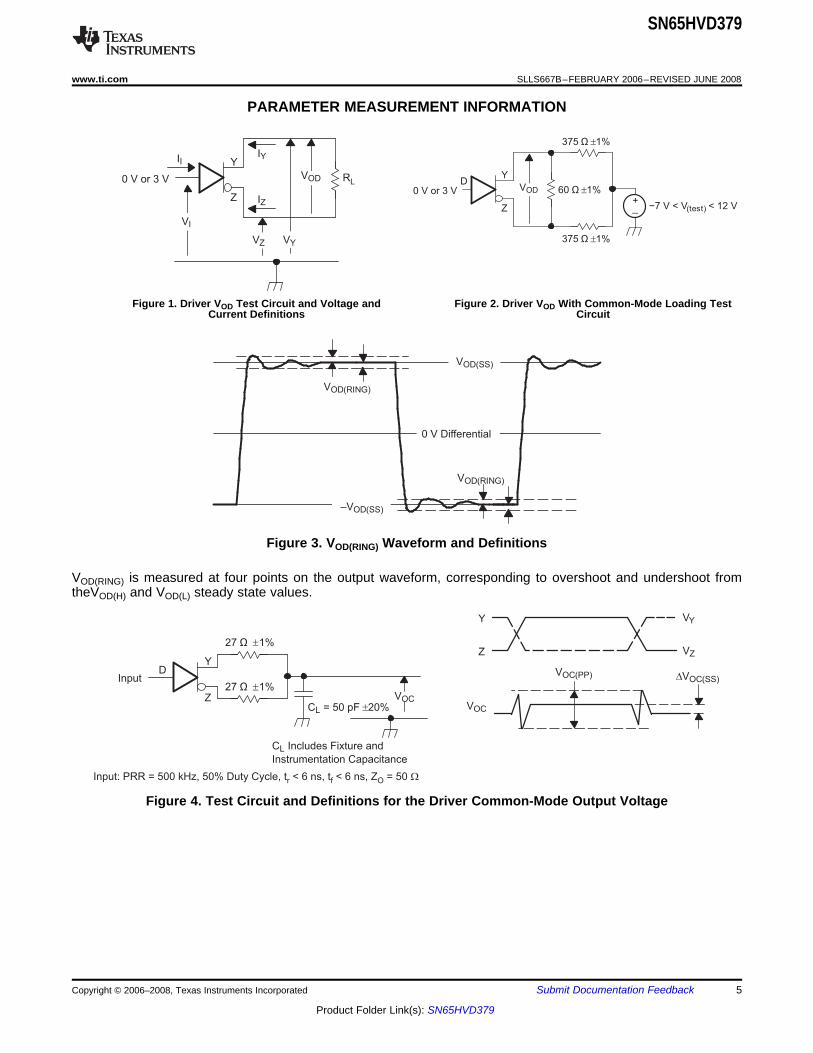
Figure 1. Driver VOD Test Circuit and Voltage and Figure 2. Driver VOD With Common-Mode Loading TestCurrent Definitions Circuit
Figure 3. VOD(RING) Waveform and Definitions
VOD(RING) is measured at four points on the output waveform, corresponding to overshoot and undershoot fromtheVOD(H) and VOD(L) steady state values.
Figure 4. Test Circuit and Definitions for the Driver Common-Mode Output Voltage
Copyright © 2006–2008, Texas Instruments Incorporated Submit Documentation Feedback 5
Product Folder Link(s): SN65HVD379
Y
ZW
W
»
»
Generator: PRR = 500 kHz, 50% Duty Cycle, t < 6 ns, t < 6 ns, Z = 50r f O W
VIDVA
VB
IOA
B
IB VO
R
IA
VICVA + VB
2
Input
Generator 50 Ω
VO
1.5 V
1.5 V 1.5 V
3 V
VOH
VOL
1.5 V10%
1.5 V
tPLH tPHL
tr tf
90%
VI
VO
CL = 15 pF
±20%
C Includes Fixture and Instrumentation CapacitanceL
A
BVI
R
0 V
90%
10%
Generator: PRR = 500 kHz, 50% Duty Cycle, t < 6 ns, t < 6 ns, Z = 50r f O W
B
A
R
100 W
±1%
+
-
Pulse Generator
15 ms duration
1% Duty Cycle
t t 100 nsr f £,
Z
Y
D
100 W±1%
+
-
SN65HVD379
SLLS667B–FEBRUARY 2006–REVISED JUNE 2008 .................................................................................................................................................... www.ti.com
PARAMETER MEASUREMENT INFORMATION (continued)
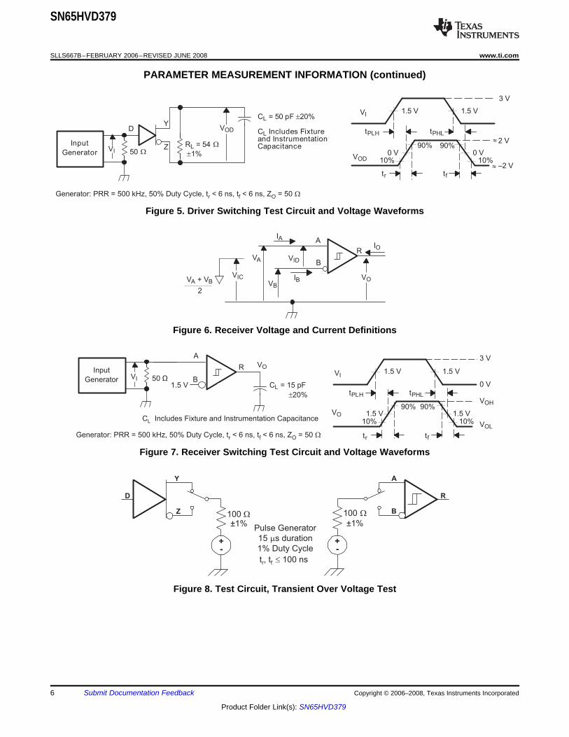
Figure 5. Driver Switching Test Circuit and Voltage Waveforms
Figure 6. Receiver Voltage and Current Definitions
Figure 7. Receiver Switching Test Circuit and Voltage Waveforms
Figure 8. Test Circuit, Transient Over Voltage Test
6 Submit Documentation Feedback Copyright © 2006–2008, Texas Instruments Incorporated
Product Folder Link(s): SN65HVD379
EQUIVALENT INPUT AND OUTPUT SCHEMATIC DIAGRAMS
VCC
Input
470 W
125 kW
9 V
D Input
R322 V
22 V
Input
R2
R1
VCC
B Input
16 V
16 V
Y and Z Outputs
Output
VCC
R322 V
22 V
Input
R2
R1
VCC
A Input
VCC
5 W
Output
R Output
9 V
SN65HVD379
www.ti.com .................................................................................................................................................... SLLS667B–FEBRUARY 2006–REVISED JUNE 2008
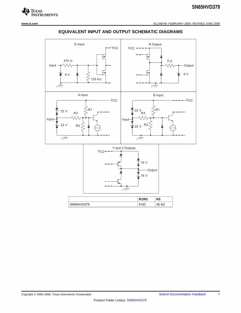
R1/R2 R3SN65HVD379 9 kΩ 45 kΩ
Copyright © 2006–2008, Texas Instruments Incorporated Submit Documentation Feedback 7
Product Folder Link(s): SN65HVD379

TYPICAL CHARACTERISTICS
30
35
40
45
50
55
0 5 10 15 20 25
Signaling Rate - Mbps
I-
RM
S S
up
ply
Cu
rren
t -
mA
CC
T = 25°C R = 54
= V C = 50 pF
DE = V
A L
CC L
CC
W
RE
V = 3.3 VCC
–200
–150
–100
–50
50
0
100
150
200
250
–7 –4 –1 2 5 8 11 14
V - Bus Input Voltage - VI
I-
Bu
s In
pu
t C
urr
en
t -
AI
m
T = 25°C
= 0 V
DE = 0 V
A
RE
V = 3.3 VCC
–0.02
0
0.02
0.04
0.06
0.08
0.1
0.12
0.14
0 0.5 1 1.5 2 2.5 3 3.5
V - Low-Level Output Voltage - VOL
I-
Dri
ver
Lo
w-L
evel O
utp
ut
Cu
rren
t -
AO
L
V = 3.3 V
DE = V
D = 0 V
CC
CC
–0.13
–0.11
–0.09
–0.07
–0.05
–0.03
–0.01
0.01
0 0.5 1 1.5 2 2.5 3 3.5
V - High-Level Output Voltage - VOH
I-
Dri
ve
r H
igh
-Le
ve
l O
utp
ut
Cu
rre
nt
-A
OH
V = 3.3 V
DE = V
D = 0 V
CC
CC
SN65HVD379
SLLS667B–FEBRUARY 2006–REVISED JUNE 2008 .................................................................................................................................................... www.ti.com
RMS SUPPLY CURRENT BUS INPUT CURRENTvs vs
SIGNALING RATE BUS INPUT VOLTAGE
Figure 9. Figure 10.
DRIVER LOW-LEVEL OUTPUT CURRENT DRIVER HIGH-LEVEL OUTPUT CURRENTvs vs
LOW-LEVEL OUTPUT VOLTAGE HIGH-LEVEL OUTPUT VOLTAGE
Figure 11. Figure 12.
8 Submit Documentation Feedback Copyright © 2006–2008, Texas Instruments Incorporated
Product Folder Link(s): SN65HVD379
1.8
1.9
2.0
2.1
2.2
–40 –15 10 35 60 85
T - Free-Air Temperature - °CA
V-
Dri
ve
r D
iffe
ren
tia
l O
utp
ut
Vo
lta
ge
- V
OD
V = 3.3 V
DE = V
D =
CC
CC
VCC
0
5
10
15
20
25
30
35
40
0 0.5 1 1.5 2 2.5 3 3.5
V - Supply Voltage - VCC
I-
Dri
ver
Ou
tpu
t C
urr
en
t -
mA
O
T = 25°C
R = 54
D = V
DE = V
A
L
CC
CC
W
SN65HVD379
www.ti.com .................................................................................................................................................... SLLS667B–FEBRUARY 2006–REVISED JUNE 2008
TYPICAL CHARACTERISTICS (continued)
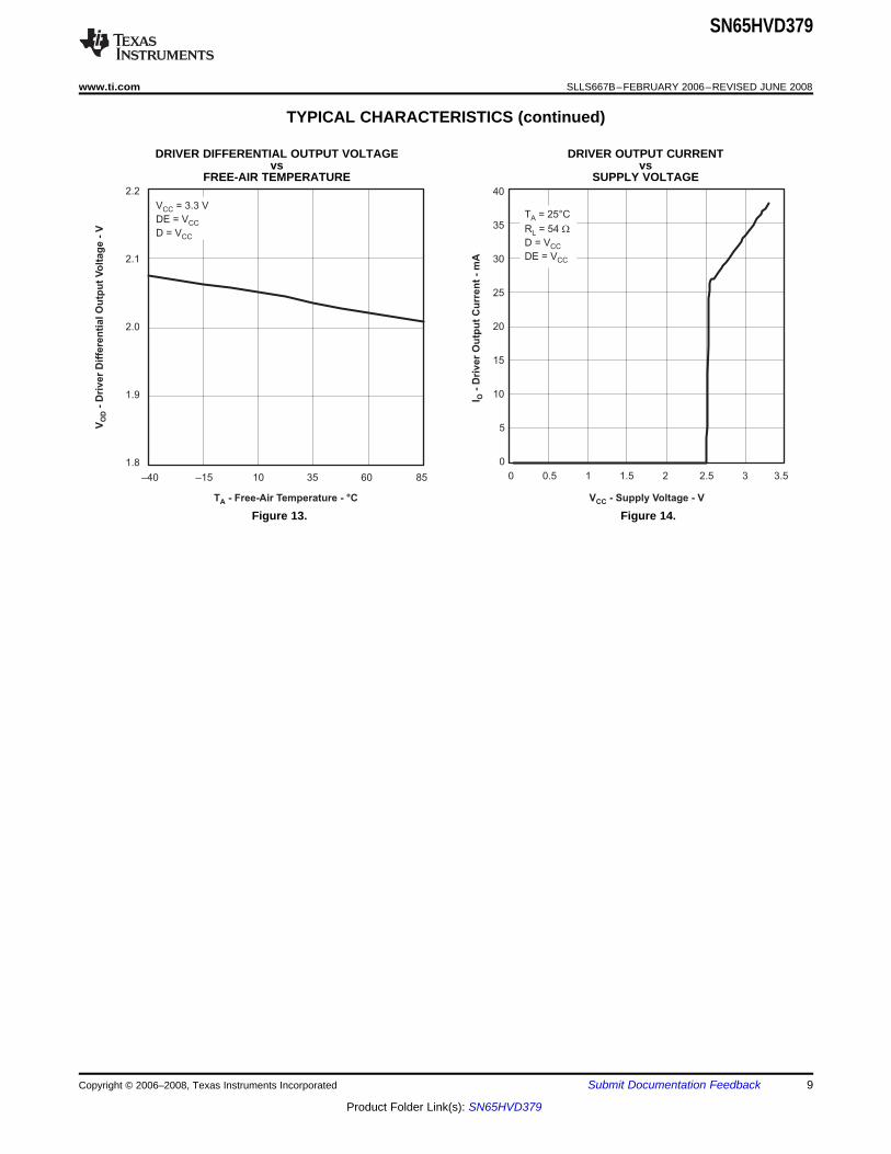
DRIVER DIFFERENTIAL OUTPUT VOLTAGE DRIVER OUTPUT CURRENTvs vs
FREE-AIR TEMPERATURE SUPPLY VOLTAGE
Figure 13. Figure 14.
Copyright © 2006–2008, Texas Instruments Incorporated Submit Documentation Feedback 9
Product Folder Link(s): SN65HVD379

PACKAGE OPTION ADDENDUM
www.ti.com 7-Aug-2014
Addendum-Page 1
PACKAGING INFORMATION
Orderable Device Status(1)
Package Type PackageDrawing
Pins PackageQty
Eco Plan(2)
Lead/Ball Finish(6)
MSL Peak Temp(3)
Op Temp (°C) Device Marking(4/5)
Samples
SN65HVD379D ACTIVE SOIC D 8 75 Green (RoHS& no Sb/Br)
CU NIPDAU Level-1-260C-UNLIM -40 to 85 VP379
SN65HVD379DG4 ACTIVE SOIC D 8 75 Green (RoHS& no Sb/Br)
CU NIPDAU Level-1-260C-UNLIM -40 to 85 VP379
SN65HVD379DR ACTIVE SOIC D 8 2500 Green (RoHS& no Sb/Br)
CU NIPDAU Level-1-260C-UNLIM -40 to 85 VP379
SN65HVD379DRG4 ACTIVE SOIC D 8 2500 Green (RoHS& no Sb/Br)
CU NIPDAU Level-1-260C-UNLIM -40 to 85 VP379
(1) The marketing status values are defined as follows:ACTIVE: Product device recommended for new designs.LIFEBUY: TI has announced that the device will be discontinued, and a lifetime-buy period is in effect.NRND: Not recommended for new designs. Device is in production to support existing customers, but TI does not recommend using this part in a new design.PREVIEW: Device has been announced but is not in production. Samples may or may not be available.OBSOLETE: TI has discontinued the production of the device.
(2) Eco Plan - The planned eco-friendly classification: Pb-Free (RoHS), Pb-Free (RoHS Exempt), or Green (RoHS & no Sb/Br) - please check http://www.ti.com/productcontent for the latest availabilityinformation and additional product content details.TBD: The Pb-Free/Green conversion plan has not been defined.Pb-Free (RoHS): TI's terms "Lead-Free" or "Pb-Free" mean semiconductor products that are compatible with the current RoHS requirements for all 6 substances, including the requirement thatlead not exceed 0.1% by weight in homogeneous materials. Where designed to be soldered at high temperatures, TI Pb-Free products are suitable for use in specified lead-free processes.Pb-Free (RoHS Exempt): This component has a RoHS exemption for either 1) lead-based flip-chip solder bumps used between the die and package, or 2) lead-based die adhesive used betweenthe die and leadframe. The component is otherwise considered Pb-Free (RoHS compatible) as defined above.Green (RoHS & no Sb/Br): TI defines "Green" to mean Pb-Free (RoHS compatible), and free of Bromine (Br) and Antimony (Sb) based flame retardants (Br or Sb do not exceed 0.1% by weightin homogeneous material)
(3) MSL, Peak Temp. - The Moisture Sensitivity Level rating according to the JEDEC industry standard classifications, and peak solder temperature.
(4) There may be additional marking, which relates to the logo, the lot trace code information, or the environmental category on the device.
(5) Multiple Device Markings will be inside parentheses. Only one Device Marking contained in parentheses and separated by a "~" will appear on a device. If a line is indented then it is a continuationof the previous line and the two combined represent the entire Device Marking for that device.
(6) Lead/Ball Finish - Orderable Devices may have multiple material finish options. Finish options are separated by a vertical ruled line. Lead/Ball Finish values may wrap to two lines if the finishvalue exceeds the maximum column width.
PACKAGE OPTION ADDENDUM
www.ti.com 7-Aug-2014
Addendum-Page 2
Important Information and Disclaimer:The information provided on this page represents TI's knowledge and belief as of the date that it is provided. TI bases its knowledge and belief on informationprovided by third parties, and makes no representation or warranty as to the accuracy of such information. Efforts are underway to better integrate information from third parties. TI has taken andcontinues to take reasonable steps to provide representative and accurate information but may not have conducted destructive testing or chemical analysis on incoming materials and chemicals.TI and TI suppliers consider certain information to be proprietary, and thus CAS numbers and other limited information may not be available for release.
In no event shall TI's liability arising out of such information exceed the total purchase price of the TI part(s) at issue in this document sold by TI to Customer on an annual basis.
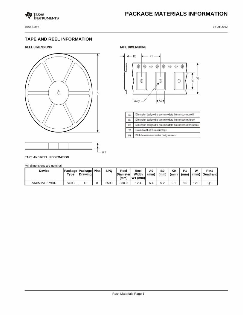
TAPE AND REEL INFORMATION
*All dimensions are nominal
Device PackageType
PackageDrawing
Pins SPQ ReelDiameter
(mm)
ReelWidth
W1 (mm)
A0(mm)
B0(mm)
K0(mm)
P1(mm)
W(mm)
Pin1Quadrant
SN65HVD379DR SOIC D 8 2500 330.0 12.4 6.4 5.2 2.1 8.0 12.0 Q1
PACKAGE MATERIALS INFORMATION
www.ti.com 14-Jul-2012
Pack Materials-Page 1

*All dimensions are nominal
Device Package Type Package Drawing Pins SPQ Length (mm) Width (mm) Height (mm)
SN65HVD379DR SOIC D 8 2500 367.0 367.0 35.0
PACKAGE MATERIALS INFORMATION
www.ti.com 14-Jul-2012
Pack Materials-Page 2


IMPORTANT NOTICETexas Instruments Incorporated and its subsidiaries (TI) reserve the right to make corrections, enhancements, improvements and otherchanges to its semiconductor products and services per JESD46, latest issue, and to discontinue any product or service per JESD48, latestissue. Buyers should obtain the latest relevant information before placing orders and should verify that such information is current andcomplete. All semiconductor products (also referred to herein as “components”) are sold subject to TI’s terms and conditions of salesupplied at the time of order acknowledgment.TI warrants performance of its components to the specifications applicable at the time of sale, in accordance with the warranty in TI’s termsand conditions of sale of semiconductor products. Testing and other quality control techniques are used to the extent TI deems necessaryto support this warranty. Except where mandated by applicable law, testing of all parameters of each component is not necessarilyperformed.TI assumes no liability for applications assistance or the design of Buyers’ products. Buyers are responsible for their products andapplications using TI components. To minimize the risks associated with Buyers’ products and applications, Buyers should provideadequate design and operating safeguards.TI does not warrant or represent that any license, either express or implied, is granted under any patent right, copyright, mask work right, orother intellectual property right relating to any combination, machine, or process in which TI components or services are used. Informationpublished by TI regarding third-party products or services does not constitute a license to use such products or services or a warranty orendorsement thereof. Use of such information may require a license from a third party under the patents or other intellectual property of thethird party, or a license from TI under the patents or other intellectual property of TI.Reproduction of significant portions of TI information in TI data books or data sheets is permissible only if reproduction is without alterationand is accompanied by all associated warranties, conditions, limitations, and notices. TI is not responsible or liable for such altereddocumentation. Information of third parties may be subject to additional restrictions.Resale of TI components or services with statements different from or beyond the parameters stated by TI for that component or servicevoids all express and any implied warranties for the associated TI component or service and is an unfair and deceptive business practice.TI is not responsible or liable for any such statements.Buyer acknowledges and agrees that it is solely responsible for compliance with all legal, regulatory and safety-related requirementsconcerning its products, and any use of TI components in its applications, notwithstanding any applications-related information or supportthat may be provided by TI. Buyer represents and agrees that it has all the necessary expertise to create and implement safeguards whichanticipate dangerous consequences of failures, monitor failures and their consequences, lessen the likelihood of failures that might causeharm and take appropriate remedial actions. Buyer will fully indemnify TI and its representatives against any damages arising out of the useof any TI components in safety-critical applications.In some cases, TI components may be promoted specifically to facilitate safety-related applications. With such components, TI’s goal is tohelp enable customers to design and create their own end-product solutions that meet applicable functional safety standards andrequirements. Nonetheless, such components are subject to these terms.No TI components are authorized for use in FDA Class III (or similar life-critical medical equipment) unless authorized officers of the partieshave executed a special agreement specifically governing such use.Only those TI components which TI has specifically designated as military grade or “enhanced plastic” are designed and intended for use inmilitary/aerospace applications or environments. Buyer acknowledges and agrees that any military or aerospace use of TI componentswhich have not been so designated is solely at the Buyer's risk, and that Buyer is solely responsible for compliance with all legal andregulatory requirements in connection with such use.TI has specifically designated certain components as meeting ISO/TS16949 requirements, mainly for automotive use. In any case of use ofnon-designated products, TI will not be responsible for any failure to meet ISO/TS16949.Products ApplicationsAudio www.ti.com/audio Automotive and Transportation www.ti.com/automotiveAmplifiers amplifier.ti.com Communications and Telecom www.ti.com/communicationsData Converters dataconverter.ti.com Computers and Peripherals www.ti.com/computersDLP® Products www.dlp.com Consumer Electronics www.ti.com/consumer-appsDSP dsp.ti.com Energy and Lighting www.ti.com/energyClocks and Timers www.ti.com/clocks Industrial www.ti.com/industrialInterface interface.ti.com Medical www.ti.com/medicalLogic logic.ti.com Security www.ti.com/securityPower Mgmt power.ti.com Space, Avionics and Defense www.ti.com/space-avionics-defenseMicrocontrollers microcontroller.ti.com Video and Imaging www.ti.com/videoRFID www.ti-rfid.comOMAP Applications Processors www.ti.com/omap TI E2E Community e2e.ti.comWireless Connectivity www.ti.com/wirelessconnectivity
Mailing Address: Texas Instruments, Post Office Box 655303, Dallas, Texas 75265Copyright © 2014, Texas Instruments Incorporated