32/40-bit ieee dsp - atmel
TRANSCRIPT

Rev. 4153I-AERO–04/07
1
Features• Superscalar IEEE Floating-Point-Processor
• Off-Chip Harvard Architecture Maximizes Signal Processing Performance
• 50 ns, 20 MIPS Instruction Rate, Single Cycle Execution
• 60 MFLOPS Peak, 40 MFLOPS Sustained Performance
• 1024-Point Complex FFT Benchmark: 0.975 ms
• Divide (y/x): 300 ns
• Inverse Square Root (1/ /x): 450 ns
• 32-bit Single-Precision and 40-bit Extended-Precision IEEE Floating-Point Data
Formats
• 32-bit Fixed-Point Formats, Integer and Fractional, with 80-bit Accumulators
• IEEE Exception Handling with Interrupt on Exception
• Three Independent Computation Units: Multiplier, ALU, and Barrel Shifter
• Dual Data Address Generators with Indirect, Immediate, Modulo, and Bit Reverse
Addressing Modes
• Two Off-Chip Memory Transfers in Parallel with Instruction Fetch and Single-Cycle
Multiply and ALU Operations
• Multiply with Add and Subtract for FFT Butterfly Computation
• Efficient Program Sequencing with Zero Overhead Looping: Single-Cycle Loop Setup
• Single-Cycle Register File Context Switch
• 23ns External RAM Access Time for Zero-Wait-State, 40 ns Instruction Execution
• IEEE JTAG Standard 1149.1 Test Access Port and On-chip Emulation Circuitry
• 223 CPGA package for breadboarding
• 256 Multi-layer Quad Flat Pack, Flat Leads, For Flight Models
• Fully compatible with Analog Devices ADSP-21020
• No Single Event Latch-up below a LET Threshold of 80 MeV/mg/cm2
• Tested up to a Total Dose of 100 krads (Si) according to MIL STD 883 Method 1019
• SEU Error Note in GEO Orbit Better than 5E-7 Error/Device/Day (worst case)
• For 25 MHz Specification, Contact Atmel for Availability
• Quality Grades - ESCC with 9512/002 and QML-Q or V with 5962-99539
Introduction
Atmel is manufacturing a radiation hard version of the Analog Devices ADSP-21020
32/40-bit Floating-Point DSP.
The product is pin and code compatible with ADI product, making system develop-
ment straight forward and cost effective, using existing development tools and
algorithms.
Notes: 1. Design using patent from INPG-CNRS Denis BESSOT/Raoul VELAZCO
2. Product licensed from Analog Devices Inc.
Rad. Hard
32/40-bit IEEE
Floating Point
DSP
TSC21020F

2
TSC21020F4153H–AERO–04/07
Functional Block Diagram
3
TSC21020F
4153H–AERO–04/07
General Description The TSC21020F is single-chip IEEE floating-point processor optimized for digital signal
processing applications (1). Its architecture is similar to that of Analog Devices' ADSP-
2100 family of fixed-point DSP processors.
Fabricated in a high-speed, low-power and radiation hard CMOS process, the
TSC21020F has a 50ns instruction cycle time. With a high-performance On-chip instruc-
tion cache, the TSC21020F can execute every instruction in a single cycle.
The TSC21020F features:
Independent Parallel Computation Units
The arithmetic/logic unit (ALU), multiplier and shifter perform single-cycle instructions.
The units are architecturally arranged in parallel, maximizing computational throughput.
A single multifunction instruction executes parallel ALU and multiplier operations. These
computation units support IEEE 32-bit single-precision floating-point, extended preci-
sion 40-bit floating-point, and 32-bit fixed-point data formats.
Data Register File A general-purpose data register file is used for transferring data between the computa-
tion units and the data buses, and for storing intermediate results. This 10-port (16-
register) register file, combined with the TSC21020F's Harvard architecture, allows
unconstrained data flow between computation units and off-chip memory.
Single-Cycle Fetch of Instruction and Two Operands
The TSC21020F uses a modified Harvard architecture in which data memory stores
data and program memory stores both instructions and data. Because of its separate
program and data memory buses and On-chip instruction cache, the processor can
simultaneously fetch an operand from data memory, an operand from program memory,
and an instruction from the cache, all in a single cycle.
Memory Interface Addressing of external memory devices by the TSC21020F is facilitated by On-chip
decoding of high-order address lines to generate memory bank select signals. Separate
control lines are also generated for simplified addressing of page-mode DRAM. The
TSC21020F provides programmable memory wait states, and external memory
acknowledge controls allow interfacing to peripheral devices with variable access times.
Instruction Cache The TSC21020F includes a high performance instruction cache that enables three-bus
operation for fetching an instruction and two data values. The cache is selective-only the
instructions whose fetches conflict with program memory data accesses are cached.
This allows full-speed execution of core, looped operations such as digital filter multiply-
accumulates and FFT butterfly processing.
Hardware Circular Buffers
The TSC21020F provides hardware to implement circular buffers in memory, which are
common in digital filters and Fourier transform implementations. It handles address
pointer wraparound, reducing overhead (thereby increasing performance) and simplify-
ing implementation. Circular buffers can start and end at any location.
Flexible Instruction Set The TSC21020F's 48-bit instruction word accommodates a variety of parallel opera-
tions, for concise programming. For example, the TSC21020F can conditionally execute
a multiply, an add, a subtract and a branch in a single instruction.
1. It is fully compatible with Analog Devices ADSP-21020
4
TSC21020F4153H–AERO–04/07
Development System The TSC21020F is supported with a complete set of software and hardware develop-
ment tools from Analog Devices. The ADSP-21000 Family Development System from
Analog Devices includes development software, an evaluation board and an in-circuit
emulator.
Assembler Creates relocatable, COFF (Common Object File Format) object files from ADSP-21xxx
assembly source code. It accepts standard C preprocessor directives for conditional
assembly and macro processing. The algebraic syntax of the ADSP-21xxx assembly
language facilitates coding and debugging of DSP algorithms.
Linker/Librarian The Linker processes separately assembled object files and library files to create a sin-
gle executable program. It assigns memory locations to code and to data in accordance
with a user-defined architecture file that describes the memory and I/O configuration of
the target system. The Librarian allows you to group frequently used object files into a
single library file that can be linked with your main program.
Simulator The Simulator performs interactive, instruction-level simulation of ADSP-21xxx code
within the hardware configuration described by a system architecture file. It flags illegal
operations and supports full symbolic disassembly. It provides an easy-to-use, window
oriented, graphical user interface that is identical to the one used by the ADSP- 21020
EZ-ICE Emulator. Commands are accessed from pull-down menus with a mouse.
PROM Splitter Formats an executable file into files that can be used with an industry-standard PROM
programmer.
C Compiler and Runtime Library
The C Compiler complies with ANSI specifications. It takes advantage of the
TSC21020F's high-level language architectural features and incorporates optimizing
algorithms to speed up the execution of code. It includes an extensive runtime library
with over 100 standard and DSP-specific functions.
C Source Level Debugger
A full-featured C source level debugger that works with the simulator or EZ-ICE emula-
tor to allow debugging of assembler source, C source, or mixed assembler and C.
Numerical C Compiler Supports ANSI Standard (X3J11.1) Numerical C as defined by the Numeric C Exten-
sions Group. The compiler accepts C source input containing Numerical C extensions
for array selection, vector math operations, complex data types, circular pointers, and
variably dimensioned arrays, and outputs ADSP-21xxx assembly language source
code.
ADSP- 21020 EZ-LAB® Evaluation Board
The EZ-LAB Evaluation Board is a general-purpose, standalone TSC21020F system
that includes 32K words of program memory and 32K words of data memory as well as
analog I/O. A PC RS-232 download path enables the user to download and run pro-
grams directly on the EZ-LAB. In addition, it may be used in conjunction with the EZ-ICE
Emulator to provide a powerful software debug environment.
ADSP- 21020 EZ-ICE® Emulator
This in-circuit emulator provides the system designer with a PC-based development
environment that allows non-intrusive access to the TSC21020F's internal registers
through the processor's 5-pin JTAG Test Access Port. This use of On-chip emulation
circuitry enables reliable, full-speed performance in any target. The emulator uses the
same graphical user interface as the ADSP- 21020 Simulator, allowing an easy transi-
5
TSC21020F
4153H–AERO–04/07
tion from software to hardware debug. (See "Target System Requirements for Use of
EZ-ICE Emulator" on page 27.)
®EZ-LAB and EZ-ICE are registered trademarks of Analog Devices, Inc.
Additional Information This data sheet provides a general overview of TSC21020F functionality. For additional
information on the architecture and instruction set of the processor, refer to the ADSP-
21020 User's Manual. For development system and programming reference informa-
tion, refer to the ADSP-21000 Family Development Software Manuals and the ADSP-
21020 Programmer's Quick Reference.

6
TSC21020F4153H–AERO–04/07
Architecture
Overview
Figure 1 shows a block diagram of the TSC21020F. The processor features:
• Three Computation Units (ALU, Multiplier, and Shifter) with a Shared Data Register
File
• Two Data Address Generators (DAG 1, DAG 2)
• Program Sequencer with Instruction Cache
• 32-bit Timer
• Memory Buses and Interface
• JTAG Test Access Port and On-chip Emulation Support
Computation Units The TSC21020F contains three independent computation units: an ALU, a multiplier
with fixed-point accumulator, and a shifter. In order to meet a wide variety of processing
needs, the computation units process data in three formats: 32-bit fixed-point, 32-bit
floating-point and 40-bit floating-point. The floating-point operations are single-precision
IEEE-compatible (IEEE Standard 754/854). The 32-bit floating-point format is the stan-
dard IEEE format, whereas the 40-bit IEEE extended- precision format has eight
additional LSBs of mantissa for greater accuracy.
The multiplier performs floating-point and fixed-point multiplication as well as fixed-point
multiply/add and multiply/subtract operations. Integer products are 64 bits wide, and the
accumulator is 80 bits wide. The ALU performs 45 standard arithmetic and logic opera-
tions, supporting both fixed-point and floating-point formats. The shifter performs 19
different operations on 32-bit operands. These operations include logical and arithmetic
shifts, bit manipulation, field deposit, and extract and derive exponent operations.
The computation units perform single-cycle operations; there is no computation pipeline.
The three units are connected in parallel rather than serially, via multiple-bus connec-
tions with the 10-port data register file. The output of any computation unit may be used
as the input of any unit on the next cycle. In a multifunction computation, the ALU and
multiplier perform independent, simultaneous operations.
Data Register File The TSC21020F's general-purpose data register file is used for transferring data
between the computation units and the data buses, and for storing intermediate results.
The register file has two sets (primary and alternate) of sixteen 40-bit registers each, for
fast context switching.

7
TSC21020F
4153H–AERO–04/07
Figure 1. TSC21020F Block Diagram
With a large number of buses connecting the registers to the computation units, data
flow between computation units and from/to off-chip memory is unconstrained and free
from bottlenecks. The 10-port register file and Harvard architecture of the TSC21020F
allow the following nine data transfers to be performed every cycle:
• Off-chip read/write of two operands to or from the register file
• Two operands supplied to the ALU
• Two operands supplied to the multiplier
• Two results received from the ALU and multiplier (three, if the ALU operation is a
combined addition/subtraction).
The processor's 48-bit orthogonal instruction word supports fully parallel data transfer
and arithmetic operations in the same instruction.
Address Generators and Program Sequencer
Two dedicated address generators and a program sequencer supply addresses for
memory accesses. Because of this, the computation units need never be used to calcu-
late addresses. Because of its instruction cache, the TSC21020F can simultaneously
fetch an instruction and data values from both off-chip program memory and off-chip
data memory in a single cycle.
The data address generators (DAGs) provide memory addresses when external mem-
ory data is transferred over the parallel memory ports to or from internal registers. Dual
data address generators enable the processor to output two simultaneous addresses for
dual operand reads and writes. DAG 1 supplies 32-bit addresses to data memory. DAG
2 supplies 24-bit addresses to program memory for program memory data accesses.
Each DAG keeps track of up to eight address pointers, eight modifiers, eight buffer
length values and eight base values. A pointer used for indirect addressing can be mod-
ified by a value in a specified register, either before (premodify) or after (post-modify)

8
TSC21020F4153H–AERO–04/07
the access. To implement automatic modulo addressing for circular buffers, the
TSC21020F provides buffer length registers that can be associated with each pointer.
Base values for pointers allow circular buffers to be placed at arbitrary locations. Each
DAG register has an alternate register that can be activated for fast context switching.
The program sequencer supplies instruction addresses to program memory. It controls
loop iterations and evaluates conditional instructions. To execute looped code with zero
overhead, the TSC21020F maintains an internal loop counter and loop stack. No explicit
jump or decrement instructions are required to maintain the loop.
The TSC21020F derives its high clock rate from pipelined fetch, decode and execute
cycles. Approximately 70% of the machine cycle is available for memory accesses; con-
sequently, TSC21020F systems can be built using slower and therefore less expensive
memory chips.
Instruction Cache The program sequencer includes a high performance, selective instruction cache that
enables three-bus operation for fetching an instruction and two data values. This two-
way, set-associative cache holds 32 instructions. The cache is selective (only the
instructions whose fetches conflict with program memory data accesses are cached), so
the TSC21020F can perform a program memory data access and can execute the cor-
responding instruction in the same cycle. The program sequencer fetches the instruction
from the cache instead of from program memory, enabling the TSC21020F to simulta-
neously access data in both program memory and data memory.
Context Switching Many of the TSC21020F's registers have alternate register sets that can be activated
during interrupt servicing to facilitate a fast context switch. The data registers in the reg-
ister file, DAG registers and the multiplier result register all have alternate sets.
Registers active at reset are called primary registers; the others are called alternate reg-
isters. Bits in the MODE1 control register determine which registers are active at any
particular time.
The primary/alternate select bits for each half of the register file (top eight or bottom
eight registers) are independent. Likewise, the top four and bottom four register sets in
each DAG have independent primary/alternate select bits. This scheme allows passing
of data between contexts.
Interrupts The TSC21020F has four external hardware interrupts, nine internally generated inter-
rupts, and eight software interrupts. For the external interrupts and the internal timer
interrupt, the TSC21020F automatically stacks the arithmetic status and mode (MODE1)
registers when servicing the interrupt, allowing five nesting levels of fast service for
these interrupts.
An interrupt can occur at any time while the TSC21020F is executing a program. Inter-
nal events that generate interrupts include arithmetic exceptions, which allow for fast
trap handling and recovery.
Timer The programmable interval timer provides periodic interrupt generation. When enabled,
the timer decrements a 32-bit count register every cycle. When this count register
reaches zero, the TSC21020F generates an interrupt and asserts its TIMEXP output.
The count register is automatically reloaded from a 32-bit period register and the count
resumes immediately.

9
TSC21020F
4153H–AERO–04/07
System Interface Figure 2 shows an TSC21020F basic system configuration.
The external memory interface supports memory- mapped peripherals and slower mem-
ory with a user-defined combination of programmable wait states and hardware
acknowledge signals. Both the program memory and data memory interfaces support
addressing of page-mode DRAMs.
The TSC21020F's internal functions are supported by four internal buses: the program
memory address (PMA) and data memory address (DMA) buses are used for
addresses associated with program and data memory. The program memory data
(PMD) and data memory data (DMD) buses are used for data associated with the two
memory spaces. These buses are extended off chip. Four data memory select (DMS)
signals select one of four user-configurable banks of data memory. Similarly, two pro-
gram memory select (PMS) signals select between two user-configurable banks of
program memory. All banks are independently programmable for 0-7 wait states.
The PX registers permit passing data between program memory and data memory
spaces. They provide a bridge between the 48-bit PMD bus and the 40-bit DMD bus or
between the 40-bit register file and the PMD bus.
The PMA bus is 24 bits wide allowing direct access of up to 16M words of mixed instruc-
tion code and data. The PMD is 48 bits wide to accommodate the 48-bit instruction
width. For access of 40-bit data the lower 8 bits are unused. For access of 32-bit data
the lower 16 bits are ignored.
The DMA bus is 32 bits wide allowing direct access of up to 4 Gigawords of data. The
DMD bus is 40 bits wide. For 32-bit data, the lower 8 bits are unused. The DMD bus pro-
vides a path for the contents of any register in the processor to be transferred to any
other register or to any external data memory location in a single cycle. The data mem-
ory address comes from one of two sources: an absolute value specified in the
instruction code (direct addressing) or the output of a data address generator (indirect
addressing).
Figure 2. Basic System Configuration
External devices can gain control of the processor's memory buses from the
TSC21020F by means of the bus request/grant signals (BR and BG). To grant its buses
in response to a bus request, the TSC21020F halts internal operations and places its
10
TSC21020F4153H–AERO–04/07
program and data memory interfaces in a high impedance state. In addition, three-state
controls (DTMS and PMTS) allow an external device to place either the program or data
memory interface in a high impedance state without affecting the other interface and
without halting the TSC21020F unless it requires a memory access from the affected
interface. The three-state controls make it easy for an external cache controller to hold
the TSC21020F off the bus while it updates an external cache memory.
JTAG Test and Emulation Support
The TSC21020F implements the boundary scan testing provisions specified by IEEE
Standard 1149.1 of the Joint Testing Action Group (JTAG). The TSC21020F's test
access port and On-chip JTAG circuitry is fully compliant with the IEEE 1149.1 specifi-
cation. The test access port enables boundary scan testing of circuitry connected to the
TSC21020F's I/O pins.
The TSC21020F also implements On-chip emulation through the JTAG test access port.
The processor's eight sets of breakpoint range registers enable program execution at
full speed until reaching a desired breakpoint address range. The processor can then
halt and allow reading/writing of all the processor's internal registers and external mem-
ories through the JTAG port.

11
TSC21020F
4153H–AERO–04/07
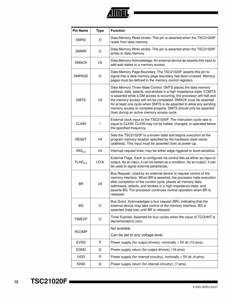
Pin Descriptions This section describes the pins of the TSC21020F. When groups of pins are identified
with subscripts, e.g. PMD47-0, the highest numbered pin is the MSB (in this case,
PMD47). Inputs identified as synchronous (S) must meet timing requirements with
respect to CLKIN (or with respect to TCK for TMS, TDI, and TRST). Those that are
asynchronous (A) can be asserted asynchronously to CLKIN.
Note: O = Output; I = Input; S = Synchronous; A = Asynchronous; P = Power Supply; G =
Ground.
Pin Name Type Function
PMA23-0 OProgram Memory Address. The TSC21020F outputs an address in
program memory on these pins.
PMD47-0 I/O
Program Memory Data. The TSC21020F inputs and outputs data and
instructions on these pins. 32-bit fixed-point data and 32-bit single-
precision floating-point data is transferred over bits 47-16 of the PMD
bus.
PMS1-0 O
Program Memory Select lines. These pins are asserted as chip selects
for the corresponding banks of program memory. Memory banks must
be defined in the memory control registers. These pins are decoded
program memory address lines and provide an early indication of a
possible bus cycle.
PMRD OProgram Memory Read strobe. This pin is asserted when the
TSC21020F reads from program memory.
PMWR OProgram Memory Write strobe. This pin is asserted when the
TSC21020F writes to program memory.
PMACK I/SProgram Memory Acknowledge. An external device de-asserts this
input to add wait states to a memory access.
PMPAGE O
Program Memory Page Boundary. The TSC21020F asserts this pin to
signal that a program memory page boundary has been crossed.
Memory pages must be defined in the memory control registers.
PMTS I/S
Program Memory Three-State Control. PMTS places the program
memory address, data, selects, and strobes in a high-impedance state.
If PMTS is asserted while a PM access is occurring, the processor will
halt and the memory access will not be completed. PMACK must be
asserted for at least one cycle when PMTS is de-asserted to allow any
pending memory access to complete properly. PMTS should only be
asserted (low) during an active memory access cycle.
DMA31-0 OData Memory Address. The TSC21020F outputs an address in data
memory on these pins.
DMD39-0 I/O
Data Memory Data. The TSC21020F inputs and outputs data on these
pins. 32-bit fixed-point data and 32-bit single-precision floating-point
data is transferred over bits 39-8 of the DMD bus.
DMS3-0 O
Data Memory Select lines. These pins are asserted as chip selects for
the corresponding banks of data memory. Memory banks must be
defined in the memory control registers. These pins are decoded data
memory address lines and provide an early indication of a possible bus
cycle.
12
TSC21020F4153H–AERO–04/07
DMRD OData Memory Read strobe. This pin is asserted when the TSC21020F
reads from data memory.
DMWR OData Memory Write strobe. This pin is asserted when the TSC21020F
writes to data memory.
DMACK I/SData Memory Acknowledge. An external device de-asserts this input to
add wait states to a memory access.
DMPAGE O
Data Memory Page Boundary. The TSC21020F asserts this pin to
signal that a data memory page boundary has been crossed. Memory
pages must be defined in the memory control registers.
DMTS I/S
Data Memory Three-State Control. DMTS places the data memory
address, data, selects, and strobes in a high-impedance state. If DMTS
is asserted while à DM access is occurring, the processor will halt and
the memory access will not be completed. DMACK must be asserted
for at least one cycle when DMTS is de-asserted to allow any pending
memory access to complete properly. DMTS should only be asserted
(low) during an active memory access cycle.
CLKIN I
External clock input to the TSC21020F. The instruction cycle rate is
equal to CLKIN. CLKIN may not be halted, changed, or operated below
the specified frequency.
RESET I/A
Sets the TSC21020F to a known state and begins execution at the
program memory location specified by the hardware reset vector
(address). This input must be asserted (low) at power-up.
IRQ3-0 I/A Interrupt request lines; may be either edge-riggered or level-sensitive.
FLAG3-0 I/O/A
External Flags. Each is configured via control bits as either an input or
output. As an input, it can be tested as a condition. As an output, it can
be used to signal external peripherals.
BR I/A
Bus Request. Used by an external device to request control of the
memory interface. When BR is asserted, the processor halts execution
after completion of the current cycle, places all memory data,
addresses, selects, and strobes in a high-impedance state, and
asserts BG. The processor continues normal operation when BR is
released.
BG O
Bus Grant. Acknowledges a bus request (BR), indicating that the
external device may take control of the memory interface. BG is
asserted (held low) until BR is released.
TIMEXP OTimer Expired. Asserted for four cycles when the value of TCOUNT is
decremented to zero.
RCOMPNot available
Can be set to any voltage level.
EVDD P Power supply (for output drivers), nominally + 5V dc (10 pins).
EGND G Power supply return (for output drivers); (16 pins).
IVDD P Power supply (for internal circuitry), nominally + 5V dc (4 pins).
IGND G Power supply return (for internal circuitry); (7 pins).
Pin Name Type Function

13
TSC21020F
4153H–AERO–04/07
TCK I Test Clock. Provides an asynchronous clock for JTAG boundary scan.
TMS I/STest Mode Select. Used to control the test state machine. TMS has a
20 kΩ internal pull-up resistor.
TDI I/STest Data Input. Provides serial data for the boundary scan logic. TDI
has a 20 kΩ internal pull-up resistor.
TDO O Test Data Output. Serial scan output of the boundary scan path.
TRST I/A
Test Reset. Resets the test state machine. TRST must be asserted
(pulsed low) after power-up or held low for proper operation of the
TSC21020F. TRST has a 20 kΩ internal pull-up resistor.
NCNo Connect. No Connects are reserved pins that must be left open and
unconnected.
Table 1. PGA Pin Configuration
PGA
Location
Pin
Name
PGA
Location
Pin
Name
PGA
Location
Pin
Name
PGA
Location
Pin
Name
G16 DMA0 B5 DMD25 K1 PMD9 L16 TIMEXP
G17 DMA1 B6 DMD26 L3 PMD10 U12 RCOMP
F18 DMA2 D6 DMD27 L2 PMD11 T11 CLKIN
F17 DMA3 C6 DMD28 M1 PMD12 T14 TRST
F16 DMA4 A8 DMD29 M2 PMD13 R12 TD0
F15 DMA5 C7 DMD30 M3 PMD14 S13 TDI
E18 DMA6 D7 DMD31 M4 PMD15 U16 TMS
E17 DMA7 B7 DMD32 N2 PMD16 U14 TCK
E16 DMA8 B8 DMD33 N3 PMD17 H18 EGND
D18 DMA9 A10 DMD34 P1 PMD18 A3 EGND
E15 DMA10 C8 DMD35 P2 PMD19 A7 EGND
D17 DMA11 D8 DMD36 N4 PMD20 A11 EGND
D16 DMA12 B9 DMD37 S1 PMD21 A15 EGND
C18 DMA13 C9 DMD38 P3 PMD22 E1 EGND
C17 DMA14 B10 DMD39 R2 PMD23 G1 EGND
D15 DMA15 D10 DMS0 P4 PMD24 L1 EGND
B18 DMA16 C11 DMS1 R3 PMD25 L18 EGND
B17 DMA17 A12 DMS2 S2 PMD26 R1 EGND
C16 DMA18 B11 DMS3 T1 PMD27 R18 EGND
D14 DMA19 T13 DMWR S3 PMD28 T18 EGND
C15 DMA20 S11 DMRD R4 PMD29 U5 EGND
B16 DMA21 B12 DMPAGE T2 PMD30 U7 EGND
Pin Name Type Function

14
TSC21020F4153H–AERO–04/07
A16 DMA22 S12 DMTS U1 PMD31 U11 EGND
D13 DMA23 T12 DMACK T3 PMD32 U15 EGND
C14 DMA24 L17 PMA0 R5 PMD33 D11 IGND
B15 DMA25 M18 PMA1 S4 PMD34 G4 IGND
B14 DMA26 M15 PMA2 U2 PMD35 G15 IGND
D12 DMA27 M16 PMA3 S5 PMD36 L4 IGND
C13 DMA28 M17 PMA4 T4 PMD37 L15 IGND
A14 DMA29 N17 PMA5 R6 PMD38 R7 IGND
B13 DMA30 N16 PMA6 U3 PMD39 R11 IGND
C12 DMA31 N15 PMA7 U4 PMD40 A5 EVDD
H3 DMD0 P18 PMA8 S6 PMD41 A9 EVDD
H4 DMD1 P17 PMA9 T6 PMD42 A13 EVDD
E2 DMD2 R17 PMA10 S7 PMD43 J1 EVDD
G3 DMD3 S18 PMA11 U6 PMD44 J18 EVDD
D1 DMD4 P15 PMA12 T7 PMD45 N1 EVDD
D2 DMD5 P16 PMA13 R8 PMD46 N18 EVDD
F3 DMD6 S17 PMA14 S8 PMD47 U9 EVDD
C1 DMD7 R16 PMA15 R13 PMS0 U13 EVDD
C2 DMD8 R15 PMA16 T15 PMS1 K18 EVDD
F4 DMD9 U18 PMA17 U8 PMWR D9 IVDD
E3 DMD10 S16 PMA18 S9 PMRD J4 IVDD
D3 DMD11 T17 PMA19 S14 PMPAGE J15 IVDD
B1 DMD12 U17 PMA20 T8 PMTS R9 IVDD
E4 DMD13 R14 PMA21 U10 PMACK C10 NC
B2 DMD14 S15 PMA22 A17 BG S10 NC
C3 DMD15 T16 PMA23 A18 BR T10 NC
A2 DMD16 F2 PMD0 H16 FLAG0 T9 NC
D4 DMD17 F1 PMD1 H15 FLAG1 K17 NC
B3 DMD18 J3 PMD2 H17 FLAG2 T5 NC
A4 DMD19 H2 PMD3 G18 FLAG3 G2 NC
C4 DMD20 H1 PMD4 J17 IRQ0
B4 DMD21 J2 PMD5 J16 IRQ1
D5 DMD22 K4 PMD6 K16 IRQ2
A6 DMD23 K3 PMD7 K15 IRQ3
C5 DMD24 K2 PMD8 R10 RESET
Table 1. PGA Pin Configuration (Continued)
PGA
Location
Pin
Name
PGA
Location
Pin
Name
PGA
Location
Pin
Name
PGA
Location
Pin
Name

15
TSC21020F
4153H–AERO–04/07
Table 2. MQFP Pin Configuration
MQFP_F
Location
Pin
Name
MQFP_F
Location
Pin
Name
MQFP_F
Location
Pin
Name
MQFP_F
Location
Pin
Name
1 IGND 65 IGND 129 IGND 193 IGND
2 IVDD 66 IVDD 130 IVDD 194 IVDD
3 DMD19 67 PMD25 131 PMA19 195 DMA15
4 DMD18 68 PMD26 132 PMA18 196 EGND
5 DMD17 69 PMD27 133 PMA17 197 DMA16
6 DMD16 70 EVDD 134 PMA16 198 DMA17
7 EGND 71 PMD28 135 EGND 199 DMA18
8 DMD15 72 PMD29 136 PMA15 200 DMA19
9 DMD14 73 PMD30 137 PMA14 201 EVDD
10 DMD13 74 PMD31 138 PMA13 202 DMA20
11 DMD12 75 EGND 139 PMA12 203 DMA21
12 EVDD 76 PMD32 140 EVDD 204 DMA22
13 DMD11 77 PMD33 141 PMA11 205 DMA23
14 DMD10 78 PMD34 142 PMA10 206 EGND
15 DMD9 79 PMD35 143 PMA9 207 DMA24
16 DMD8 80 EVDD 144 PMA8 208 DMA25
17 IGND 81 IGND 145 IGND 209 IGND
18 IVDD 82 IVDD 146 IVDD 210 IVDD
19 EGND 83 PMD36 147 EGND 211 DMA26
20 DMD7 84 PMD37 148 PMA7 212 DMA27
21 DMD6 85 PMD38 149 PMA6 213 EVDD
22 DMD5 86 PMD39 150 PMA5 214 DMA28
23 DMD4 87 EGND 151 PMA4 215 DMA29
24 EVDD 88 PMD40 152 EVDD 216 DMA30
25 DMD3 89 PMD41 153 PMA3 217 DMA31
26 DMD2 90 PMD42 154 PMA2 218 EGND
27 DMD1 91 PMD43 155 PMA1 219 DMPAGE
28 DMD0 92 EVDD 156 PMA0 220 BR
29 EGND 93 PMD44 157 EGND 221 BG
30 PMD0 94 PMD45 158 TIMEXP 222 DMS0
31 PMD1 95 PMD46 159 EVDD 223 DMS1
32 PMD2 96 PMD47 160 EGND 224 EVDD
33 IGND 97 IGND 161 IGND 225 IGND
34 IVDD 98 IVDD 162 IVDD 226 IVDD
35 PMD3 99 EGND 163 IRQ3 227 DMS2

16
TSC21020F4153H–AERO–04/07
Instruction Set
Summary
The TSC21020F instruction set provides a wide variety of programming capabilities.
Every instruction assembles into a single word and can execute in a single processor
cycle. Multifunction instructions enable simultaneous multiplier and ALU operations, as
well as computations executed in parallel with data transfers. The addressing power of
the TSC21020F gives flexibility in moving data both internally and externally. The
TSC21020F assembly language uses an algebraic syntax for ease of coding and
readability.
36 EVDD 100 PMTS 164 IRQ2 228 DMS3
37 PMD4 101 PMWR 165 IRQ1 229 DMD39
38 PMD5 102 PMACK 166 IRQ0 230 DMD38
39 PMD6 103 PMRD 167 EVDD 231 EGND
40 PMD7 104 RCMP 168 FLAG0 232 DMD37
41 EGND 105 EVDD 169 FLAG1 233 DMD36
42 PMD8 106 RESET 170 FLAG2 234 DMD35
43 PMD9 107 CLKIN 171 FLAG3 235 DMD34
44 PMD10 108 DMRD 172 EGND 236 EVDD
45 PMD11 109 DMACK 173 DMA0 237 DMD33
46 EVDD 110 DMWR 174 DMA1 238 DMD32
47 PMD12 111 EVDD 175 DMA2 239 DMD31
48 PMD13 112 DMTS 176 DMA3 240 DMD30
49 IGND 113 IGND 177 IGND 241 IGND
50 IVDD 114 IVDD 178 IVDD 242 IVDD
51 PMD14 115 TCK 179 EVDD 243 EGND
52 PMD15 116 TMS 180 DMA4 244 DMD29
53 EGND 117 TDI 181 DMA5 245 DMD28
54 PMD16 118 TDO 182 DMA6 246 DMD27
55 PMD17 119 TRST 183 DMA7 247 DMD26
56 PMD18 120 PMPAGE 184 EGND 248 EVDD
57 PMD19 121 PMS0 185 DMA8 249 DMD25
58 EVDD 122 PMS1 186 DMA9 250 DMD24
59 PMD20 123 EGND 187 DMA10 251 DMD23
60 PMD21 124 PMA23 188 DMA11 252 EGND
61 PMD22 125 PMA22 189 EVDD 253 DMD22
62 PMD23 126 PMA21 190 DMA12 254 DMD21
63 EGND 127 PMA20 191 DMA13 255 DMD20
64 PMD24 128 EVDD 192 DMA14 256 EVDD
Table 2. MQFP Pin Configuration (Continued)
MQFP_F
Location
Pin
Name
MQFP_F
Location
Pin
Name
MQFP_F
Location
Pin
Name
MQFP_F
Location
Pin
Name

17
TSC21020F
4153H–AERO–04/07
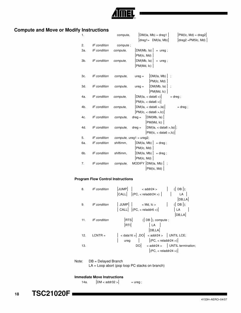
The instruction types are grouped into four categories:
• Compute and Move or Modify
• Program Flow Control
• Immediate Move
• Miscellaneous
The instruction types are numbered; there are 22 types. Some instructions have more
than one syntactical form; for example, Instruction 4 has four distinct forms. The instruc-
tion number itself has no bearing on programming, but corresponds to the opcode
recognized by the TSC21020F device.
Because of the width and orthogonality of the instruction word, there are many possible
instructions. For example, the ALU supports 21 fixed-point operations and 24 floating-
point operations; each of these operations can be the compute portion of an instruction.
The following pages provide an overview and summary of the TSC21020F instruction
set. For complete information, see the ADSP-21020 User's Manual from Analog
Devices. For additional reference information, see the ADSP- 21020 Programmer's
Quick Reference from Analog Devices.
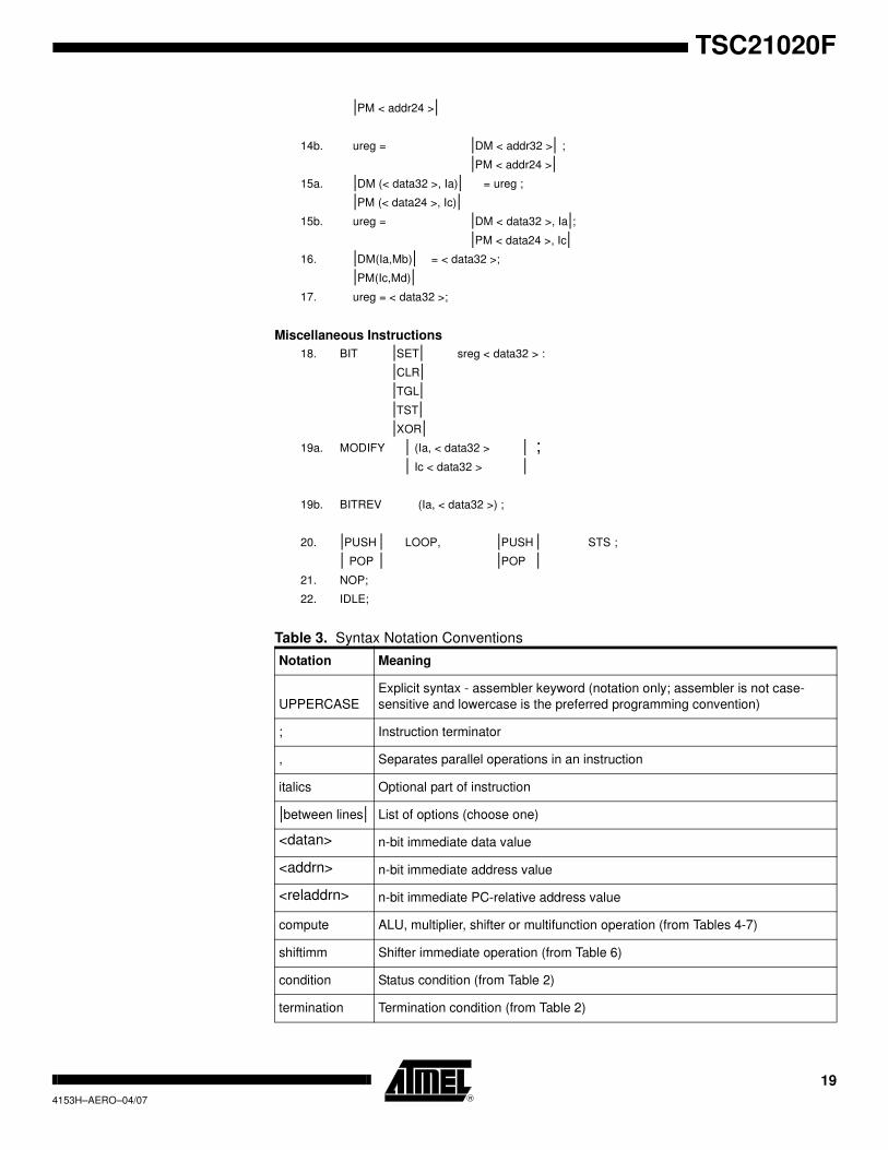
This section also contains several reference tables for using the instruction set.
• Table 3 describes the notation and abbreviations used.
• Table 4 lists all condition and termination code mnemonics.
• Table 5 lists all register mnemonics.
• Table 6 through 9 list the syntax for all compute (ALU, multiplier, shifter or
multifunction) operations.
• Table 10 lists interrupts and their vector addresses.
18
TSC21020F4153H–AERO–04/07
Compute and Move or Modify Instructions1. compute, |DM(Ia, Mb) = dreg1 | |PM(Ic, Md) = dreg2|
|dreg1= DM(Ia, Mb)| |dreg2 =PM5Ic, Md) |2. IF condition compute ;
3a. IF condition compute, |DM(Mb, Ia) | = ureg ;
|PM(Ic, Md) |3b. IF condition compute, |DM(Mb, Ia) | = ureg ;
|PM(Md, Ic) |
3c. IF condition compute, ureg = |DM(Ia, Mb) | ;
|PM(Ic, Md) |3d. IF condition compute, ureg = |DM(Mb, Ia) | ;
|PM(Md, Ic) |4a. IF condition compute, |DM(Ia, < data6 >)| = dreg ;
|PM(Ic, < data6 >)|4b. IF condition compute, |DM(Ia, < data6 >,Ia)| = dreg ;
|PM(Ic, < data6 >,Ic)|4c. IF condition compute, dreg = |DM(Mb, Ia) |
|PM(Md, Ic) |4d. IF condition compute, dreg = |DM(Ia, < data6 >,Ia)|;
|PM(Ic, < data6 >,Ic)|5. IF condition compute, ureg1 = ureg2;
6a. IF condition shiftimm, |DM(Ia, Mb) | = dreg ;
|PM(Ic, Md) |6b. IF condition shiftimm, |DM(Ia, Mb) | = dreg ;
|PM(Ic, Md) |7. IF condition compute, MODIFY |DM(Ia, Mb) | ;
|PM(Ic, Md) |
Program Flow Control Instructions
8. IF condition |JUMP| | < addr24 > | (| DB |);|CALL| |(PC, < reladdr24 >) | | LA |
|DB,LA|9. IF condition | JUMP| | < Md, Ic > | (| DB |);
| CALL| |(PC, < reladdr6 >)| | LA | |DB,LA|
11. IF condition |RTS| (| DB |), compute ; |RTI| | LA |
|DB,LA|12. LCNTR = | < data16 >| ,DO| < addr24 > | UNTIL LCE;
| ureg | |(PC, < reladdr24 >)| 13. DO| < addr24 > | UNTIL termination;
|(PC, < reladdr24 >)|
Note: DB = Delayed Branch
LA = Loop abort (pop loop PC stacks on branch)
Immediate Move Instructions
14a. |DM < addr32 >| = ureg ;
19
TSC21020F
4153H–AERO–04/07
|PM < addr24 >|
14b. ureg = |DM < addr32 >| ;
|PM < addr24 >|15a. |DM (< data32 >, Ia)| = ureg ;
|PM (< data24 >, Ic)|15b. ureg = |DM < data32 >, Ia|;
|PM < data24 >, Ic|16. |DM(Ia,Mb)| = < data32 >;
|PM(Ic,Md)|17. ureg = < data32 >;
Miscellaneous Instructions
18. BIT |SET| sreg < data32 > :
|CLR||TGL||TST||XOR|
19a. MODIFY | (Ia, < data32 > | ;| Ic < data32 > |
19b. BITREV (Ia, < data32 >) ;
20. |PUSH | LOOP, |PUSH | STS ;
| POP | |POP |21. NOP;
22. IDLE;
Table 3. Syntax Notation Conventions
Notation Meaning
UPPERCASE
Explicit syntax - assembler keyword (notation only; assembler is not case-
sensitive and lowercase is the preferred programming convention)
; Instruction terminator
, Separates parallel operations in an instruction
italics Optional part of instruction
|between lines| List of options (choose one)
<datan> n-bit immediate data value
<addrn> n-bit immediate address value
<reladdrn> n-bit immediate PC-relative address value
compute ALU, multiplier, shifter or multifunction operation (from Tables 4-7)
shiftimm Shifter immediate operation (from Table 6)
condition Status condition (from Table 2)
termination Termination condition (from Table 2)

20
TSC21020F4153H–AERO–04/07
ureg Universal register (from Table 3)
sreg System register (from Table 3)
dreg R15-R0, F15-F0; register file location
Ia I7-I0; DAG1 index register
Mb M7-M0; DAG1 modify register
Ic I15-I8; DAG2 index register
Md M15-M8; DAG2 modify register
Table 3. Syntax Notation Conventions
Notation Meaning
21
TSC21020F
4153H–AERO–04/07
Table 4. Condition and Termination Codes
Name Description
eq ALU equal to zero
ne ALU not equal to zero
ge ALU greater than or equal to zero
lt ALU less than zero
le ALU less than or equal to zero
gt ALU greater than zero
ac ALU carry
not ac Not ALU carry
av ALU overflow
not av Not ALU overflow
mv Multiplier overflow
not mv Not multiplier overflow
ms Multiplier sign
not ms Not multiplier sign
sv Shifter overflow
not sv Not shifter overflow
sz Shifter zero
not sz Not shifter zero
flag0_in Flag 0
not flag0_in Not Flag 0
flag1_in Flag 1
not flag1_in Not Flag 1
flag2_in Flag 2
not flag2_in Not Flag 2
flag3_in Flag 3
not flag3_in Not Flag 3
tf Bit test flag
not tf Not bit test flag
lce Loop counter expired (DO UNTIL)
not lce Loop counter not expired (IF)
forever Always False (DO UNTIL)
true Always True (IF)
Note: In a conditional instruction, the execution of the entire instruction is based on the speci-
fied condition.

22
TSC21020F4153H–AERO–04/07
Table 5. Universal Registers
Name Function
Register file
R15-R0 Register file locations
Program Sequencer
PC(1) Program counter; address of instruction currently executing
PCSTK Top of PC stack
PCSTKP PC stack pointer
FADDR(1) Fetch address
DADDR(1) Decode address
LADDR Loop termination address, code; top of loop address stack
CURLCNTR Current loop counter; top of loop count stack
LCNTR Loop count for next nested counter-controlled loop
Data Address Generators
I7-I0 DAG1 index registers
M7-M0 DAG1 modify registers
L7-L0 DAG1 length registers
B7-B0 DAG1 base registers
I15-I8 DAG2 index registers
M15-M8 DAG2 modify registers
L15-L8 DAG2 length registers
B15-B8 DAG2 base registers
Bus Exchange
PX1 PMD-DMD bus exchange 1 (16 bits)
PX2 PMD-DMD bus exchange 2 (32 bits)
PX 48-bit PX1 and PX2 combination
Timer
TPERIOD Timer period
TCOUNT Timer counter
Memory Interface
DMWAIT Wait state and page size control for data memory
DMBANK1 Data memory bank 1 upper boundary
DMBANK2 Data memory bank 2 upper boundary

23
TSC21020F
4153H–AERO–04/07
DMBANK3 Data memory bank 3 upper boundary
DMADR(1) Copy of last data memory address
PMWAIT Wait state and page size control for program memory
PMBANK1 Program memory bank 1 upper boundary
PMADR(1) Copy of last program memory address
System Register
MODE1
Mode control bits for bit-reverse, alternate registers, interrupt nesting and
enable, ALU saturation, floating-point rounding mode and boundary
MODE2
Mode control bits for interrupt sensitivity, cache disable and freeze, timer
enable, and I/O flag configuration
IRPTL Interrupt latch
IMASK Interrupt mask
IMASKP Interrupt mask pointer (for nesting)
ASTAT Arithmetic status flags, bit test, I/O flag values, and compare accumulator
STKY
Sticky arithmetic status flags, circular buffer overflow flags, stack status flags
(not sticky)
USTAT1 User status register 1
USTAT2 User status register 2
Note: 1. Read-only
Refer to User's Manual for bit-level definitions of each register.
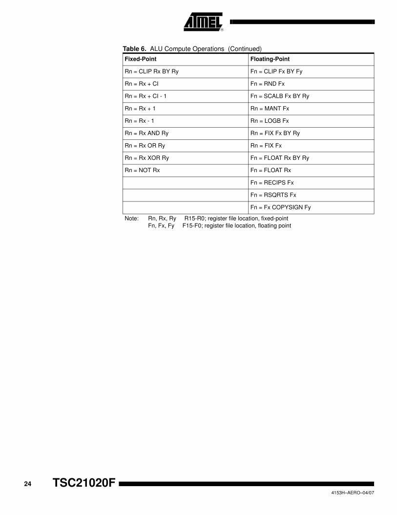
Table 6. ALU Compute Operations
Fixed-Point Floating-Point
Rn = Rx + Ry Fn = Fx + Fy
Rn = Rx - Ry Fn = Fx - Fy
Rn = Rx + Ry, Rm = Rx - Ry Fn = Fx + Fy, Fm = Fx - Fy
Rn = Rx + Ry + CI Fn = ABS (Fx + Fy)
Rn = Rx - Ry + CI - 1 Fn = ABS (Fx - Fy)
Rn = (Rx + Ry)/2 Fn = (Fx + Fy)/2
COMP(Rx, Ry) COMP(Fx, Fy)
Rn = -Rx Fn = -Fx
Rn = ABS Rx Fn = ABS Fx
Rn = PASS Rx Fn = PASS Fx
Rn = MIN(Rx, Ry) Fn = MIN(Fx, Fy)
Rn = MAX(Rx, Ry) Fn = MAX(Fx, Fy)
Table 5. Universal Registers (Continued)
Name Function
24
TSC21020F4153H–AERO–04/07
Rn = CLIP Rx BY Ry Fn = CLIP Fx BY Fy
Rn = Rx + CI Fn = RND Fx
Rn = Rx + CI - 1 Fn = SCALB Fx BY Ry
Rn = Rx + 1 Rn = MANT Fx
Rn = Rx - 1 Rn = LOGB Fx
Rn = Rx AND Ry Rn = FIX Fx BY Ry
Rn = Rx OR Ry Rn = FIX Fx
Rn = Rx XOR Ry Fn = FLOAT Rx BY Ry
Rn = NOT Rx Fn = FLOAT Rx
Fn = RECIPS Fx
Fn = RSQRTS Fx
Fn = Fx COPYSIGN Fy
Note: Rn, Rx, Ry R15-R0; register file location, fixed-point
Fn, Fx, Fy F15-F0; register file location, floating point
Table 6. ALU Compute Operations (Continued)
Fixed-Point Floating-Point

25
TSC21020F
4153H–AERO–04/07
Multiplier Compute
Operations
Rn, Rx, Ry R15-R0; register file location, fixed-point
Fn, Fx, Fy F15-F0; register file location, floating-point
MRxF MR2F, MR1F, MR0F; multiplier result accumulators, foreground
MRxB MR2B, MR1B, MR0B; multiplier result accumulators, background
(|x-input| |y-input| |data format|)| rounding |
S Signed input
U Unsigned input
I Integer input(s)
F Fractional input(s)
FR Fractional inputs, Rounded output
(SF) Default format for 1-input operations
(SSF) Default format for 2-input operations
RnMRF
MRB = Rx * Ry( S
US
UFIFR) Fn = Fx * Fy
Rn
Rn
MRF
MRB
=
=
=
=
MR F
MR B
MR F
MR B
+ Rx * Ry S
USUFIFR)
Rn
Rn
MR F
MRB
=
=
=
=
MR F
MR B
MR F
MR B
Rx * Ry ( SUS
UFIFR)
Rn
Rn
MRF
MRB
=
=
=
=
SAT M RF
SAT M RB
SAT M RF
SAT M RB
(SI)
(UI)
(SF)
(UF)
Rn
Rn
MR F
MRB
RN D MRF
RND MRB
RN D MRF
RND MRB
(SF)(UF)
MRFMRB = 0
MRxFMRxB
= Rn Rn = xFMRMRxB
26
TSC21020F4153H–AERO–04/07
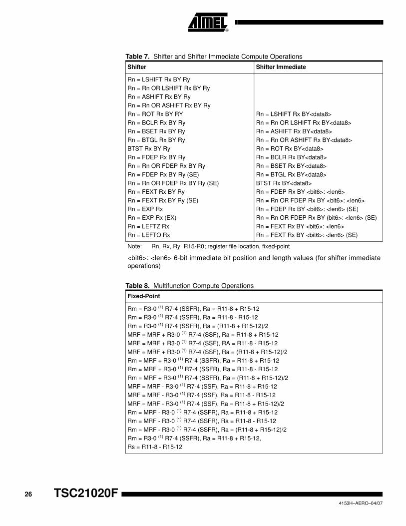
Table 7. Shifter and Shifter Immediate Compute Operations
Shifter Shifter Immediate
Rn = LSHIFT Rx BY Ry
Rn = Rn OR LSHIFT Rx BY Ry
Rn = ASHIFT Rx BY Ry
Rn = Rn OR ASHIFT Rx BY Ry
Rn = ROT Rx BY RY
Rn = BCLR Rx BY Ry
Rn = BSET Rx BY Ry
Rn = BTGL Rx BY Ry
BTST Rx BY Ry
Rn = FDEP Rx BY Ry
Rn = Rn OR FDEP Rx BY Ry
Rn = FDEP Rx BY Ry (SE)
Rn = Rn OR FDEP Rx BY Ry (SE)
Rn = FEXT Rx BY Ry
Rn = FEXT Rx BY Ry (SE)
Rn = EXP Rx
Rn = EXP Rx (EX)
Rn = LEFTZ Rx
Rn = LEFTO Rx
Rn = LSHIFT Rx BY<data8>
Rn = Rn OR LSHIFT Rx BY<data8>
Rn = ASHIFT Rx BY<data8>
Rn = Rn OR ASHIFT Rx BY<data8>
Rn = ROT Rx BY<data8>
Rn = BCLR Rx BY<data8>
Rn = BSET Rx BY<data8>
Rn = BTGL Rx BY<data8>
BTST Rx BY<data8>
Rn = FDEP Rx BY <bit6>: <len6>
Rn = Rn OR FDEP Rx BY <bit6>: <len6>
Rn = FDEP Rx BY <bit6>: <len6> (SE)
Rn = Rn OR FDEP Rx BY (bit6>: <len6> (SE)
Rn = FEXT Rx BY <bit6>: <len6>
Rn = FEXT Rx BY <bit6>: <len6> (SE)
Note: Rn, Rx, Ry R15-R0; register file location, fixed-point
<bit6>: <len6> 6-bit immediate bit position and length values (for shifter immediate
operations)
Table 8. Multifunction Compute Operations
Fixed-Point
Rm = R3-0 (1) R7-4 (SSFR), Ra = R11-8 + R15-12
Rm = R3-0 (1) R7-4 (SSFR), Ra = R11-8 - R15-12
Rm = R3-0 (1) R7-4 (SSFR), Ra = (R11-8 + R15-12)/2
MRF = MRF + R3-0 (1) R7-4 (SSF), Ra = R11-8 + R15-12
MRF = MRF + R3-0 (1) R7-4 (SSF), RA = R11-8 - R15-12
MRF = MRF + R3-0 (1) R7-4 (SSF), Ra = (R11-8 + R15-12)/2
Rm = MRF + R3-0 (1) R7-4 (SSFR), Ra = R11-8 + R15-12
Rm = MRF + R3-0 (1) R7-4 (SSFR), Ra = R11-8 - R15-12
Rm = MRF + R3-0 (1) R7-4 (SSFR), Ra = (R11-8 + R15-12)/2
MRF = MRF - R3-0 (1) R7-4 (SSF), Ra = R11-8 + R15-12
MRF = MRF - R3-0 (1) R7-4 (SSF), Ra = R11-8 - R15-12
MRF = MRF - R3-0 (1) R7-4 (SSF), Ra = R11-8 + R15-12)/2
Rm = MRF - R3-0 (1) R7-4 (SSFR), Ra = R11-8 + R15-12
Rm = MRF - R3-0 (1) R7-4 (SSFR), Ra = R11-8 - R15-12
Rm = MRF - R3-0 (1) R7-4 (SSFR), Ra = (R11-8 + R15-12)/2
Rm = R3-0 (1) R7-4 (SSFR), Ra = R11-8 + R15-12,
Rs = R11-8 - R15-12
27
TSC21020F
4153H–AERO–04/07
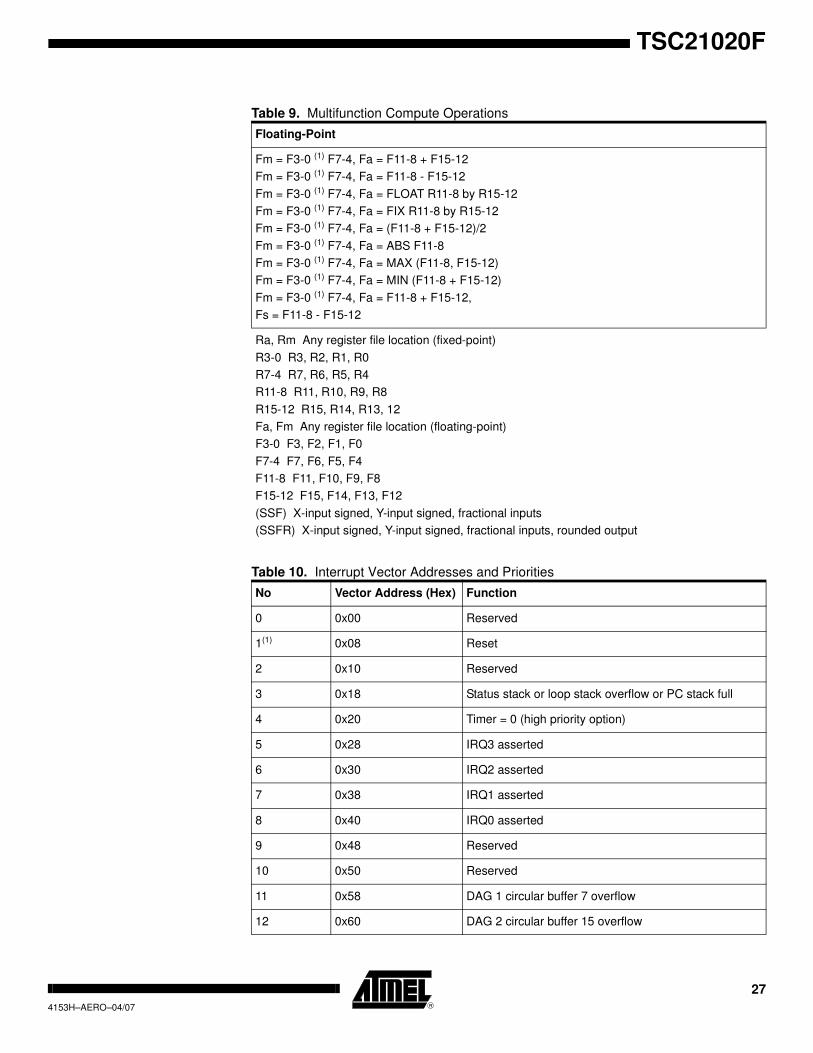
Table 9. Multifunction Compute Operations
Floating-Point
Fm = F3-0 (1) F7-4, Fa = F11-8 + F15-12
Fm = F3-0 (1) F7-4, Fa = F11-8 - F15-12
Fm = F3-0 (1) F7-4, Fa = FLOAT R11-8 by R15-12
Fm = F3-0 (1) F7-4, Fa = FIX R11-8 by R15-12
Fm = F3-0 (1) F7-4, Fa = (F11-8 + F15-12)/2
Fm = F3-0 (1) F7-4, Fa = ABS F11-8
Fm = F3-0 (1) F7-4, Fa = MAX (F11-8, F15-12)
Fm = F3-0 (1) F7-4, Fa = MIN (F11-8 + F15-12)
Fm = F3-0 (1) F7-4, Fa = F11-8 + F15-12,
Fs = F11-8 - F15-12
Ra, Rm Any register file location (fixed-point)
R3-0 R3, R2, R1, R0
R7-4 R7, R6, R5, R4
R11-8 R11, R10, R9, R8
R15-12 R15, R14, R13, 12
Fa, Fm Any register file location (floating-point)
F3-0 F3, F2, F1, F0
F7-4 F7, F6, F5, F4
F11-8 F11, F10, F9, F8
F15-12 F15, F14, F13, F12
(SSF) X-input signed, Y-input signed, fractional inputs
(SSFR) X-input signed, Y-input signed, fractional inputs, rounded output
Table 10. Interrupt Vector Addresses and Priorities
No Vector Address (Hex) Function
0 0x00 Reserved
1(1) 0x08 Reset
2 0x10 Reserved
3 0x18 Status stack or loop stack overflow or PC stack full
4 0x20 Timer = 0 (high priority option)
5 0x28 IRQ3 asserted
6 0x30 IRQ2 asserted
7 0x38 IRQ1 asserted
8 0x40 IRQ0 asserted
9 0x48 Reserved
10 0x50 Reserved
11 0x58 DAG 1 circular buffer 7 overflow
12 0x60 DAG 2 circular buffer 15 overflow
28
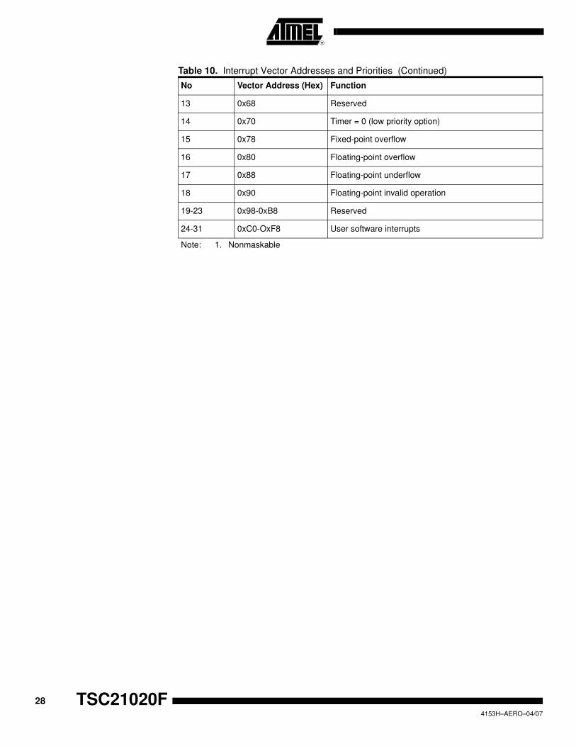
TSC21020F4153H–AERO–04/07
13 0x68 Reserved
14 0x70 Timer = 0 (low priority option)
15 0x78 Fixed-point overflow
16 0x80 Floating-point overflow
17 0x88 Floating-point underflow
18 0x90 Floating-point invalid operation
19-23 0x98-0xB8 Reserved
24-31 0xC0-OxF8 User software interrupts
Note: 1. Nonmaskable
Table 10. Interrupt Vector Addresses and Priorities (Continued)
No Vector Address (Hex) Function
29
TSC21020F
4153H–AERO–04/07
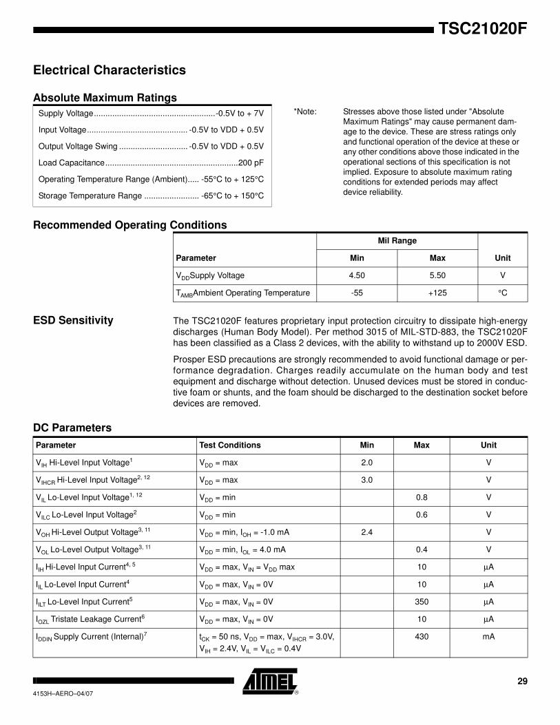
Electrical Characteristics
Absolute Maximum Ratings
Recommended Operating Conditions
ESD Sensitivity The TSC21020F features proprietary input protection circuitry to dissipate high-energy
discharges (Human Body Model). Per method 3015 of MIL-STD-883, the TSC21020F
has been classified as a Class 2 devices, with the ability to withstand up to 2000V ESD.
Prosper ESD precautions are strongly recommended to avoid functional damage or per-
formance degradation. Charges readily accumulate on the human body and test
equipment and discharge without detection. Unused devices must be stored in conduc-
tive foam or shunts, and the foam should be discharged to the destination socket before
devices are removed.
DC Parameters
Supply Voltage.....................................................-0.5V to + 7V
Input Voltage............................................ -0.5V to VDD + 0.5V
Output Voltage Swing .............................. -0.5V to VDD + 0.5V
Load Capacitance..........................................................200 pF
Operating Temperature Range (Ambient)..... -55°C to + 125°C
Storage Temperature Range ........................ -65°C to + 150°C
*Note: Stresses above those listed under "Absolute
Maximum Ratings" may cause permanent dam-
age to the device. These are stress ratings only
and functional operation of the device at these or
any other conditions above those indicated in the
operational sections of this specification is not
implied. Exposure to absolute maximum rating
conditions for extended periods may affect
device reliability.
Parameter
Mil Range
UnitMin Max
VDDSupply Voltage 4.50 5.50 V
TAMBAmbient Operating Temperature -55 +125 °C
Parameter Test Conditions Min Max Unit
VIH Hi-Level Input Voltage1 VDD = max 2.0 V
VIHCR Hi-Level Input Voltage2, 12 VDD = max 3.0 V
VIL Lo-Level Input Voltage1, 12 VDD = min 0.8 V
VILC Lo-Level Input Voltage2 VDD = min 0.6 V
VOH Hi-Level Output Voltage3, 11 VDD = min, IOH = -1.0 mA 2.4 V
VOL Lo-Level Output Voltage3, 11 VDD = min, IOL = 4.0 mA 0.4 V
IIH Hi-Level Input Current4, 5 VDD = max, VIN = VDD max 10 µA
IIL Lo-Level Input Current4 VDD = max, VIN = 0V 10 µA
IILT Lo-Level Input Current5 VDD = max, VIN = 0V 350 µA
IOZL Tristate Leakage Current6 VDD = max, VIN = 0V 10 µA
IDDIN Supply Current (Internal)7 tCK = 50 ns, VDD = max, VIHCR = 3.0V,
VIH = 2.4V, VIL = VILC = 0.4V
430 mA

30
TSC21020F4153H–AERO–04/07
AC Parameters See Figure 15 for voltage reference levels. Use the exact timing information given. Do
not attempt to derive parameters from the addition or subtraction of others. While addi-
tion or subtraction would yield meaningful results for an individual device, the values
given in this data sheet reflect statistical variations and worst cases. Consequently, you
cannot meaningfully add parameters to derive other specifications.
IDDIDLE Supply Current (Idle)8 VDD = max, VIN = 0V or VDD max 150 mA
CIN Input Capacitance9, 10 fIN = 1 MHz, TCASE = 255C, VIN = 2.5V 10 pF
Notes: 1. Applies to: PMD47-0, PMACK, PMTS, DMD39-0, DMACK, DMTS, IRQ3-0, FLAG3-0, BR, TMS, TDI.
2. Applies to: CLKIN, TCK.
3. Applies to: PMA23-0, PMD47-0, PMS1-0, PMRD, PMWR, PMPAGE, DMA31-0, DMD39-0, DMS3-0, DMRD, DMWR,
DMPAGE, FLAG3-0, TIMEXP, BG.
4. Applies to: PMACK, PMTS, DMACK, DMTS, IRQ3-0, BR, CLKIN, RESET, TCK.
5. Applies to: TMS, TDI, TRST.
6. Applies to: PMA23-0, PMD47-0, PMS1-0, PMRD, PMWR, PMPAGE, DMA31-0, DMD39-0, DMS3-0, DMRD, DMWR,
DMPAGE, FLAG3-0, TDO.
7. Applies to IVDD pins. At tCK = 50ns, IDDIN (typical) = 350 mA. See "Power Dissipation" for calculation of external (EVDD)
supply current for total supply current.
8. Applies to IVDD pins. Idle refers to TSC21020F state of operation during execution of the IDLE instruction.
9. Guaranteed but not tested.
10. Applies to all signal pins.
11. Although specified for TTL outputs, all TSC21020F outputs are CMOS-compatible and will drive to VDD and GND assuming
no dc loads.
12. Applies to RESET, TRST.
Parameter Test Conditions Min Max Unit
31
TSC21020F
4153H–AERO–04/07
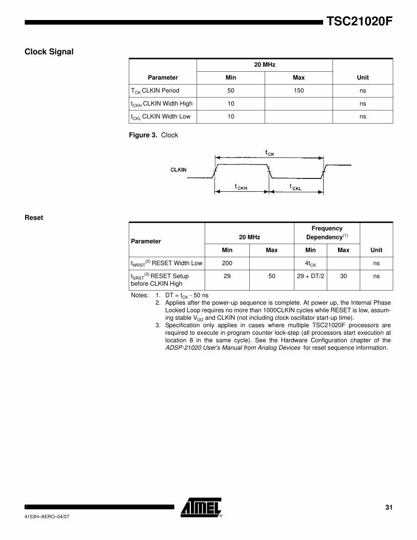
Clock Signal
Figure 3. Clock
Reset
Parameter
20 MHz
UnitMin Max
TCK CLKIN Period 50 150 ns
tCKH CLKIN Width High 10 ns
tCKL CLKIN Width Low 10 ns
Parameter20 MHz
Frequency
Dependency(1)
UnitMin Max Min Max
tWRST(2) RESET Width Low 200 4tCK ns
tSRST(3) RESET Setup
before CLKIN High
29 50 29 + DT/2 30 ns
Notes: 1. DT = tCK - 50 ns
2. Applies after the power-up sequence is complete. At power up, the Internal Phase
Locked Loop requires no more than 1000CLKIN cycles while RESET is low, assum-
ing stable VDD and CLKIN (not including clock oscillator start-up time).
3. Specification only applies in cases where multiple TSC21020F processors are
required to execute in program counter lock-step (all processors start execution at
location 8 in the same cycle). See the Hardware Configuration chapter of the
ADSP-21020 User's Manual from Analog Devices for reset sequence information.

32
TSC21020F4153H–AERO–04/07
Figure 4. Reset
Interrupts
Figure 5. Interrupts
Timer
Figure 6. TIMEXP
Parameter20 MHz
Frequency
Dependency(1) UnitMin
tSIR IRQ3-0 Setup before CLKIN High 38 38 + 3DT/4 ns
tHIR IRQ3-0 Hold after CLKIN High 0 ns
tIPW IRQ3-0 Pulse Width 55 tCK + 5 ns
Note: 1. DT = tCK - 50 ns
Meeting setup and hold guarantees interrupts will be latched in that cycle. Meeting
the pulse width is not necessary if the setup and hold is met. Likewise, meeting the
setup and hold is not necessary if the pulse width is met. See the Hardware Config-
uration chapter of the ADSP-21020 User's Manual from Analog Devices for interrupt
servicing information.
Parameter20 MHz
Frequency
Dependency(1) Unit
Max Min Max
tDTEX CLKIN High to TIMEXP 24 ns
Note: 1. DT = tCK - 50 ns
33
TSC21020F
4153H–AERO–04/07
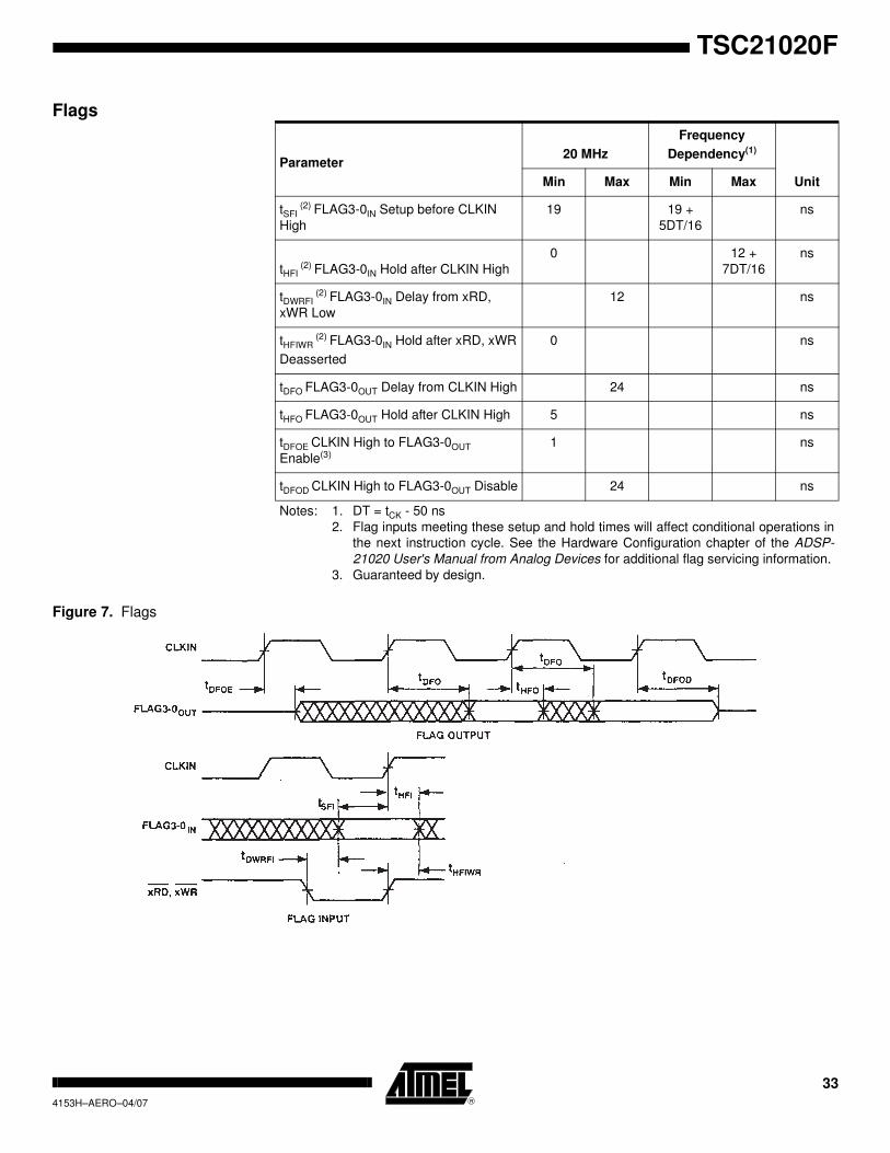
Flags
Figure 7. Flags
Parameter20 MHz
Frequency
Dependency(1)
UnitMin Max Min Max
tSFI (2) FLAG3-0IN Setup before CLKIN
High
19 19 +
5DT/16
ns
tHFI (2) FLAG3-0IN Hold after CLKIN High
0 12 +
7DT/16
ns
tDWRFI (2) FLAG3-0IN Delay from xRD,
xWR Low
12 ns
tHFIWR (2) FLAG3-0IN Hold after xRD, xWR
Deasserted
0 ns
tDFO FLAG3-0OUT Delay from CLKIN High 24 ns
tHFO FLAG3-0OUT Hold after CLKIN High 5 ns
tDFOE CLKIN High to FLAG3-0OUT
Enable(3)1 ns
tDFOD CLKIN High to FLAG3-0OUT Disable 24 ns
Notes: 1. DT = tCK - 50 ns
2. Flag inputs meeting these setup and hold times will affect conditional operations in
the next instruction cycle. See the Hardware Configuration chapter of the ADSP-
21020 User's Manual from Analog Devices for additional flag servicing information.
3. Guaranteed by design.

34
TSC21020F4153H–AERO–04/07
Bus Request/Bus Grant
Figure 8. Bus Request/Bus Grant
Parameter20 MHz
Frequency
Dependency(1) Unit
Min Max Min Max
tHBR BR Hold after CLKIN High 0 ns
tSBR BR Setup before CLKIN High 18 18+5DT/16 ns
tDMDBGL Memory Interface Disable
to BG Low(2)-2 ns
tDME CLKIN High to Memory
Interface Enable
25 25 + DT/2 ns
tDBGL CLKIN High to BG Low 22 ns
tDBGH CLKIN High to BG High 22 ns
Notes: 1. DT = tCK - 50 ns
Memory Interface = PMA23-0, PMD47-0, PMS1-0, PMRD, PMWR, PMPAGE,
DMA31-0, DMD39-0, DMS3-0, DMRD, DMWR, DMPAGE.
Buses are not granted until completion of current memory access.
See the Memory Interface chapter of the ADSP-21020 User's Manual from
Analog Devices for BG, BR cycle relationships.
2. Guaranteed by design.

35
TSC21020F
4153H–AERO–04/07
External Memory Three-State Control
Figure 9. External Memory Three-State Control
Parameter20 MHz
Frequency
Dependency(1)
UnitMin Max Min Max
tSTS XTS, Setup before CLKIN
High
14 50 14 + DT/4 tCK ns
tDADTS XTS Delay after
Address, Select
28 28 + 7DT/8 ns
tDSTS XTS, Delay after XRD,
XWR Low
16 16 + DT/2 ns
tDTSD Memory Interface
Disable before CLKIN High
0 DT/4 ns
tDTSAE XTS High to Address,
Select Enable
0 ns
Notes: 1. DT = tCK - 50 ns
XTS should only be asserted (low) during an active memory access cycle.
Memory Interface = PMA23-0, PMD47-0, PMS1-0, PMRD, PMWR, PMPAGE,
DMA31-0, DMD39-0, DMS3-0, DMRD, DMWR, DMPAGE.
Address = PMA23-0, DMA31-0, Select = PMS1-0, DMS3-0
x = PM or DM.

36
TSC21020F4153H–AERO–04/07
Memory Read
Parameter20 MHz
Frequency
Dependency(1)
Unit
Min Max Min Max
tDAD Address, Select to Data Valid 37 37 + DT ns
tDRLD xRD Low to Data Valid 24 24 + 5DT/8 ns
tHDA Data Hold from Address,
Select
0 ns
tHDRH Data Hold from xRD High -1 ns
tDAAK xACK Delay from Address 27 27 + 7DT/8 ns
tDRAK xACK Delay from xRD Low 15 15 + DT/2 ns
tSAK xACK Setup before CLKIN
High
14 14 + DT/4 ns
tHAK xACK Hold after CLKIN High 0 ns
tDARL Address, Select to xRD Low 8 8 + 3DT/8 ns
tDAP xPAGE Delay from Address,
Select
1 ns
tDCKRL CLKIN High to xRD Low 16 26 16 + DT/4 26 + DT/4 ns
tRW xRD Pulse Width
26 26 +
5DT/8
ns
tRWR xRD High to xRD, xWR Low
17 17 +
3DT/8
ns
Notes: 1. DT = tCK - 50 ns
2. x = PM or DM; Address = PMA23-0, DMA31-0; Data = PMD47-0, DMD39-0;
Select = PMS1-0, DMS3-0.

37
TSC21020F
4153H–AERO–04/07
Figure 10. Memory Read
Memory Write
Parameter20 MHz
Frequency
Dependency(1)
Unit
Min Max Min Max
tDAAK xACK Delay from
Address, Select
27 27 + 7DT/8 ns
tDWAK xACK Delay from xWR
Low
15 15 + DT/2 ns
tSAK xACK Setup before CLKIN
High
14 14 + DT/4 ns
tHAK xACK Hold after CLKIN
High
0 ns
tDAWH Address, Select to xWR
Deasserted
37 37 +
15DT/16
ns
tDAWL Address, Select to xWR
Low
11 11 + 3DT/8 ns
tWW xWR Pulse Width
26 26 +
9DT/16
ns
tDDWH Data Setup before xWR
High
23 23 + DT/2 ns
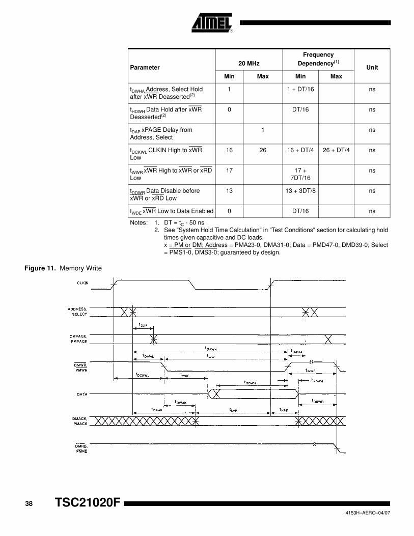
38
TSC21020F4153H–AERO–04/07
Figure 11. Memory Write
tDWHA Address, Select Hold
after xWR Deasserted(2)1 1 + DT/16 ns
tHDWH Data Hold after xWR
Deasserted(2)0 DT/16 ns
tDAP xPAGE Delay from
Address, Select
1 ns
tDCKWL CLKIN High to xWR
Low
16 26 16 + DT/4 26 + DT/4 ns
tWWR xWR High to xWR or xRD
Low
17 17 +
7DT/16
ns
tDDWR Data Disable before
xWR or xRD Low
13 13 + 3DT/8 ns
tWDE xWR Low to Data Enabled 0 DT/16 ns
Notes: 1. DT = tC - 50 ns
2. See "System Hold Time Calculation" in "Test Conditions" section for calculating hold
times given capacitive and DC loads.
x = PM or DM; Address = PMA23-0, DMA31-0; Data = PMD47-0, DMD39-0; Select
= PMS1-0, DMS3-0; guaranteed by design.
Parameter20 MHz
Frequency
Dependency(1)
Unit
Min Max Min Max
39
TSC21020F
4153H–AERO–04/07
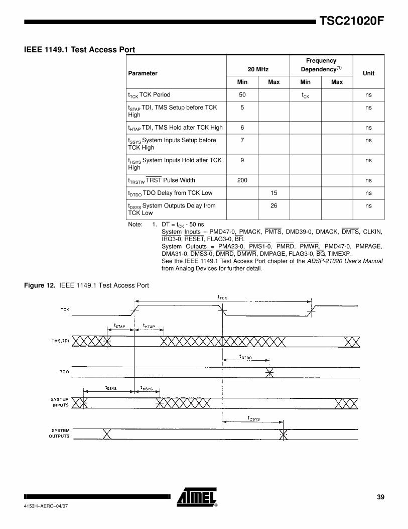
IEEE 1149.1 Test Access Port
Figure 12. IEEE 1149.1 Test Access Port
Parameter20 MHz
Frequency
Dependency(1)
Unit
Min Max Min Max
tTCK TCK Period 50 tCK ns
tSTAP TDI, TMS Setup before TCK
High
5 ns
tHTAP TDI, TMS Hold after TCK High 6 ns
tSSYS System Inputs Setup before
TCK High
7 ns
tHSYS System Inputs Hold after TCK
High
9 ns
tTRSTW TRST Pulse Width 200 ns
tDTDO TDO Delay from TCK Low 15 ns
tDSYS System Outputs Delay from
TCK Low
26 ns
Note: 1. DT = tCK - 50 ns
System Inputs = PMD47-0, PMACK, PMTS, DMD39-0, DMACK, DMTS, CLKIN,
IRQ3-0, RESET, FLAG3-0, BR.
System Outputs = PMA23-0, PMS1-0, PMRD, PMWR, PMD47-0, PMPAGE,
DMA31-0, DMS3-0, DMRD, DMWR, DMPAGE, FLAG3-0, BG, TIMEXP.
See the IEEE 1149.1 Test Access Port chapter of the ADSP-21020 User's Manual
from Analog Devices for further detail.

40
TSC21020F4153H–AERO–04/07
Figure 13. Output Enable/Disable
Test Conditions
Output Disable Time Output pins are considered to be disable when they stop driving, go into a high-imped-
ance state, and start to decay from their output high or low voltage. The time for the
voltage on the bus to decay by ∆V is dependent on the capacitive load, CL, and the load
current, IL. It can be approximated by the following equation:
The output disable time (tDIS) is the difference between tMEASURED and tDECAY as shown
in Figure 13. The time tMEASURED is the interval from when the reference signal switches
to when the output voltage decays ∆V from the measured output high or output low volt-
age. tDECAY is calculated with ∆V equal to 0.5V, and test loads CL and IL.
Output Enable Time Output pins are considered to be enabled when they have made a transition from a
high-impedance state to when they start driving. The output enable time (tENA) is the
interval from when a reference signal reaches a high or low voltage level to when the
output has reached a specified high or low trip point, as shown in the Output Enable
/Disable diagram. If multiple pins (such as the data bus) are enabled, the measurement
value is that of the first pin to start driving.
tDECAY
CL
V∆
IL
--------------=

41
TSC21020F
4153H–AERO–04/07
Figure 14. Equivalent Device Loading for AC Measurements (Includes all Fixtures)
Example System Hold Time Calculation
To determine the data output hold time in a particular system, first calculate tDECAY using
the above equation. Choose ∆V to be the difference between the TSC21020F's output
voltage and the input threshold for the device requiring the hold time. A typical ∆V will be
0.4V. CL is the total bus capacitance (per data line), and IL is the total leakage or three-
state current (per data line). The hold time will be tDECAY plus the minimum disable time
(i.e. tHDWD for the write cycle).
Figure 15. Voltage Reference Levels for AC Measurements (Except Output
Enable/Disable)
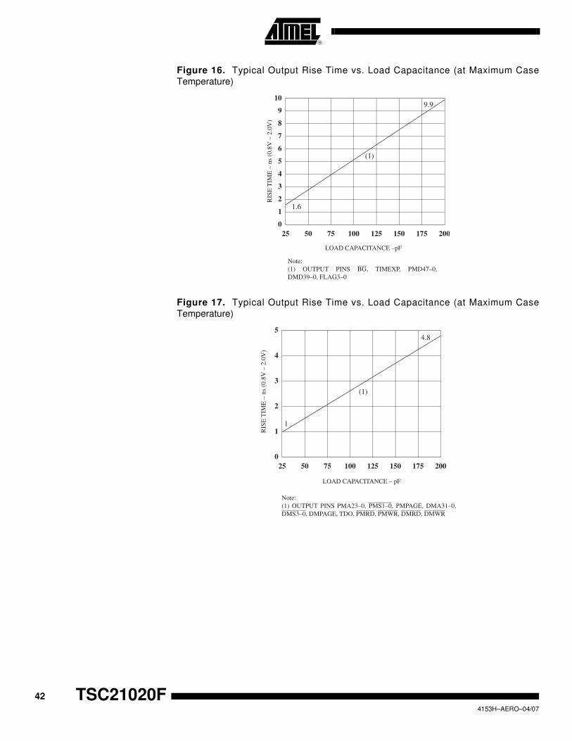
Capacitive Loading Output delays are based on standard capacitive loads: 100 pF on address, select, page
and strobe pins, and 50 pF on all others (see Figure 14). For different loads, these tim-
ing parameters should be derated. See the Hardware Configuration chapter of the
ADSP-21020 User's Manual from Analog Devices for further information on derating of
timing specifications.
Figures 16 and 17 show how the output rise time varies with capacitance. Figures 18
and 19 show how output delays vary with capacitance. Note that the graphs may not be
linear outside the ranges shown.
42
TSC21020F4153H–AERO–04/07
Figure 16. Typical Output Rise Time vs. Load Capacitance (at Maximum Case
Temperature)
Figure 17. Typical Output Rise Time vs. Load Capacitance (at Maximum Case
Temperature)
0
1
2
3
4
5
6
7
8
9
10
25 50 75 100 125 150 175 200
RIS
E T
IME
– n
s (0
.8V
– 2
.0V
)
LOAD CAPACITANCE – pF
Note:
(1) OUTPUT PINS BG, TIMEXP, PMD47– 0,
DMD39– 0, FLAG3– 0
9.9
(1)
1.6
0
1
2
3
4
5
25 50 75 100 125 150 175 200
RIS
E T
IME
– n
s (0
.8V
– 2
.0V
)
LOAD CAPACITANCE – pF
Note:
(1) OUTPUT PINS PMA23– 0, PMS1– 0, PMPAGE, DMA31– 0,
DMS3– 0, DMPAGE, TDO, PMRD, PMWR, DMRD, DMWR
4.8
(1)
1

43
TSC21020F
4153H–AERO–04/07
Figure 18. Typical Output Delay or Hold vs. Load Capacitance (at Maximum Case
Temperature)
Figure 19. Typical Output Delay or Hold vs. Load Capacitance (at Maximum Case
Temperature)
Power Dissipation Total power dissipation has two components: one due to internal circuitry and one due
to the switching of external output drivers.
Internal power dissipation is dependent on the instruction execution sequence and the
data values involved. Internal power dissipation is calculated in the following way:
PINT = IDDIN x VDD
The external component of total power dissipation is caused by the switching of output
pins. Its magnitude depends on:
1) the number of output pins that switch during each cycle(O),
2) the maximum frequency at which they can switch (f),
3) their load capacitance (C), and
– 2
0
2
4
6
8
10
12
25 50 75 100 125 150 175 200
OU
TP
UT
DE
LA
Y O
R H
OL
D –
ns
LOAD CAPACITANCE – pF
Note:
(1) OUTPUT PINS BG, TIMEXP, FLAG3– 0,
PMD47– 0, DMD39– 0
(1)
8.3
– 1.7
– 3
– 2
– 1
0
1
2
3
4
25 50 75 100 125 150 175 200
OU
TP
UT
DE
LA
Y O
R H
OL
D –
ns
LOAD CAPACITANCE – pF
Note:
(1) OUTPUT PINS PMA– 23, PMS1– 0, PMPAGE, DMA31– 0,
DMS3– 0, DMPAGE, TDO, PMRD, PMWR, DMRD, DMWR
– 2.2
(1)
2.8

44
TSC21020F4153H–AERO–04/07
4) their voltage swing (VDD).
It is calculated by:
PEXT = O x C x VDD2 x f
The load capacitance should include the processor's package capacitance (CIN). The
switching frequency includes driving the load high and then back low. Address and data
pins can drive high and low at a maximum rate of 1/(2tCK). The write strobes can switch
every cycle at a frequency of 1/tCK. Select pins switch at 1/(2tCK), but 2 DM and 2 PM
selects can switch on each cycle. If only one bank is accessed, no select line will switch.
For instance, the maximum power dissipation will be:
PINT Max = IDDINMax x VDDMax = 0,430 x 5,5 = 2,36W
PEXT Max = 0 x C x VDD Max2 x f
= 164 x 10-11 x 5.52 x 20.106 = 0.99W
Pmax = 3.4W
Power and Ground Guidelines
To achieve its fast cycle time, including instruction fetch, data access, and execution,
the TSC21020F is designed with high speed drivers on all output pins. Large peak cur-
rents may pass through a circuit board's ground and power lines, especially when many
output drivers are simultaneously charging or discharging their load capacitances.
These transient currents can cause disturbances on the power and ground lines. To
minimize these effects, the TSC21020F provides separate supply pins for its internal
logic (IGND and IVDD) and for its external drivers (EGND and EVDD).
All GND pins should have a low impedance path to ground. A ground plane is required
in TSC21020F systems to reduce this impedance, minimizing noise.
The EVDD and IVDD pins should be bypassed to the ground plane using approximately
14 high-frequency capacitors (0.1 µF ceramic). Keep each capacitor's lead and trace
length to the pins as short as possible. This low inductive path provides the TSC21020F
with the peak currents required when its output drivers switch. The capacitors' ground
leads should also be short and connect directly to the ground plane. This provides a low
impedance return path for the load capacitance of the TSC21020F's output drivers.
If a VDD plane is not used, the following recommendations apply. Traces from the + 5V
supply to the 10 EVDD pins should be designed to satisfy the minimum VDD specifica-
tion while carrying average dc currents of [IDDEX/10 x (number of EVDD pins per trace)].
IDDEX is the calculated external supply current. A similar calculation should be made for
the four IVDD pins using the IDDIN specification. The traces connecting +5V to the IVDD
pins should be separate from those connecting to the EVDD pins.
Pin Type # Pins % Switch xC xf xVDD2 PEXT
PMA
PMS
PMWR
PMD
DMA
DMS
DMWR
DMD
15
2
1
32
15
2
1
32
50
0
-
50
50
0
-
50
68 pF
68 pF
68 pF
18 pF
48 pF
48 pF
48 pF
18 pF
5 MHz
5 MHz
10 MHz
5 MHz
5 MHz
5 MHz
10 MHz
5 MHz
25V
25V
25V
25V
25V
25V
25V
25V
0.064W
0.000W
0.017W
0.036W
0.045W
0.000W
0.012W
0.036W
PEXT = 0.210W
45
TSC21020F
4153H–AERO–04/07
A low frequency bypass capacitor (20 µF tantalum) located near the junction of the
IVDD and EVDD traces is also recommended.
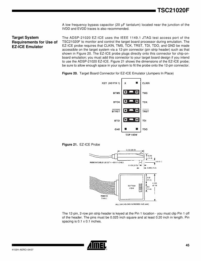
Target System Requirements for Use of EZ-ICE Emulator
The ADSP-21020 EZ-ICE uses the IEEE 1149.1 JTAG test access port of the
TSC21020F to monitor and control the target board processor during emulation. The
EZ-ICE probe requires that CLKIN, TMS, TCK, TRST, TDI, TDO, and GND be made
accessible on the target system via a 12-pin connector (pin strip header) such as that
shown in Figure 20. The EZ-ICE probe plugs directly onto this connector for chip-on-
board emulation; you must add this connector to your target board design if you intend
to use the ADSP-21020 EZ-ICE. Figure 21 shows the dimensions of the EZ-ICE probe;
be sure to allow enough space in your system to fit the probe onto the 12-pin connector.
Figure 20. Target Board Connector for EZ-ICE Emulator (Jumpers In Place)
Figure 21. EZ-ICE Probe
The 12-pin, 2-row pin strip header is keyed at the Pin 1 location - you must clip Pin 1 off
of the header. The pins must be 0.025 inch square and at least 0.20 inch in length. Pin
spacing is 0.1 x 0.1 inches.

46
TSC21020F4153H–AERO–04/07
The tip of the pins must be at least 0.10 inch higher than the tallest component under the
probe to allow clearance for the bottom of the probe. Pin strip headers are available
from vendors such as 3M, McKenzie, and Samtec.
The length of the traces between the EZ-ICE probe connector and the TSC21020F test
access port pins should be less than 1 inch. Note that the EZ-ICE probe adds two TTL
loads to the CLKIN pin of the TSC21020F.
The BMTS, BTCK, BTRST, and BTDI signals are provided so that the test access port
can also be used for board-level testing. When the connector is not being used for emu-
lation, place jumpers between the BXXX pins and the XXX pins as shown in Figure 20. If
you are not going to use the test access port for board test, tie BTRST to GND and tie or
pull up BTCK to VDD. The TRST pin must be asserted (pulsed low) after power up
(through BTRST on the connector) or held low for proper operation of the TSC21020F.
47
TSC21020F
4153H–AERO–04/07
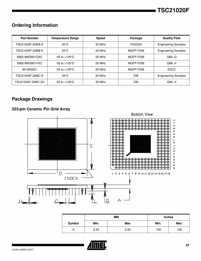
Ordering Information
Package Drawings
223-pin Ceramic Pin Grid Array
Part Number Temperature Range Speed Package Quality Flow
TSC21020F-20MA-E 25°C 20 MHz PGA223 Engineering Samples
TSC21020F-20MB-E 25°C 20 MHz MQFP-F256 Engineering Samples
5962-9953901QXC -55 to +125°C 20 MHz MQFP-F256 QML-Q
5962-9953901VXC -55 to +125°C 20 MHz MQFP-F256 QML-V
951200201 -55 to +125°C 20 MHz MQFP-F256 ESCC
TSC21020F-20MC-E 25°C 20 MHz DIE Engineering Samples
TSC21020F-20MC-SV -55 to +125°C 20 MHz DIE QML-V
Bottom View
Symbol
MM Inches
Min. Max Min. Max
A 2.54 3.30 .100 .130

48
TSC21020F4153H–AERO–04/07
256-pin MQFP-F Package Top View
C 2.54 BSC .100 BSC
D 46.74 47.75 1.840 1.880
E 46.74 47.75 1.840 1.880
H 0.41 0.51 0.16 0.20
L 3.05 3.56 .120 .140
Q 1.14 1.40 0.45 .055
Symbol
Mils MM
Min. Max Min. Max
A 0.095 0.125 2.41 3.18
C 0.004 0.008 0.10 0.20
D 2.095 2.195 53.23 55.74
D1 1.450 1.470 36.83 37.34
E 2.095 2.195 53.23 55.74
E1 1.450 1.470 36.83 37.34
e 0.020 BSC 0.508 BSC
f 0.006 0.010 0.15 0.25
A1 0.081 0.101 2.06 2.56
A2 0.002 0.014 0.05 0.36
L 0.323 0.362 8.20 9.20
N1 64 64

49
TSC21020F
4153H–AERO–04/07
N2 64 64

Printed on recycled paper.
©2007 Atmel Corporation. All rights reserved. Atmel®, logo and combinations thereof, and Everywhere You Are® are the trademarks or regis-
tered trademarks, of Atmel Corporation or its subsidiaries. Other terms and product names may be trademarks of others.
Disclaimer: The information in this document is provided in connection with Atmel products. No license, express or implied, by estoppel or otherwise,to anyintellectu-
alproperty right is granted by this document or in connection with the sale of Atmel products. EXCEPT AS SET FORTH IN ATMEL’S TERMS AND CONDI-TIONS OF
SALE LOCATED ON ATMEL’S WEB SITE, ATMEL ASSUMES NO LIABILITY WHATSOEVER AND DISCLAIMS ANY EXPRESS, IMPLIED OR STATUTORYWAR-
RANTY RELATING TO ITS PRODUCTS INCLUDING, BUT NOT LIMITED TO, THE IMPLIED WARRANTY OF MERCHANTABILITY, FITNESS FOR A PARTICU-
LARPURPOSE, OR NON-INFRINGEMENT. IN NO EVENT SHALL ATMEL BE LIABLE FOR ANY DIRECT, INDIRECT, CONSEQUENTIAL, PUNITIVE, SPECIAL
OR INCIDEN-TAL DAMAGES (INCLUDING, WITHOUT LIMITATION, DAMAGES FOR LOSS OF PROFITS, BUSINESS INTERRUPTION, OR LOSS OF INFORMA-
TION) ARISING OUTOF THE USE OR INABILITY TO USE THIS DOCUMENT, EVEN IF ATMEL HAS BEEN ADVISED OF THE POSSIBILITY OF SUCH DAM-
AGES. Atmel makes norepresentationsor warranties with respect to the accuracy or completeness of the contents of this document and reserves the right to make
changes to specificationsand product descriptions at any time without notice. Atmel does not make any commitment to update the information contained herein.
Unless specifically provided otherwise, Atmel products are not suitable for, and shall not be used in, automotive applications. Atmel’s products are not intended,
authorized, or warranted for useas components in applications intended to support or sustainlife.
Atmel Headquarters Atmel Operations
Corporate Headquarters2325 Orchard ParkwaySan Jose, CA 95131TEL 1(408) 441-0311FAX 1(408) 487-2600
EuropeAtmel SarlRoute des Arsenaux 41Case Postale 80CH-1705 FribourgSwitzerlandTEL (41) 26-426-5555FAX (41) 26-426-5500
AsiaRoom 1219Chinachem Golden Plaza77 Mody Road TsimhatsuiEast KowloonHong KongTEL (852) 2721-9778FAX (852) 2722-1369
Japan9F, Tonetsu Shinkawa Bldg.1-24-8 ShinkawaChuo-ku, Tokyo 104-0033JapanTEL (81) 3-3523-3551FAX (81) 3-3523-7581
Memory2325 Orchard ParkwaySan Jose, CA 95131TEL 1(408) 441-0311FAX 1(408) 436-4314
Microcontrollers2325 Orchard ParkwaySan Jose, CA 95131TEL 1(408) 441-0311FAX 1(408) 436-4314
La ChantrerieBP 7060244306 Nantes Cedex 3, FranceTEL (33) 2-40-18-18-18FAX (33) 2-40-18-19-60
ASIC/ASSP/Smart CardsZone Industrielle13106 Rousset Cedex, FranceTEL (33) 4-42-53-60-00FAX (33) 4-42-53-60-01
1150 East Cheyenne Mtn. Blvd.Colorado Springs, CO 80906TEL 1(719) 576-3300FAX 1(719) 540-1759
Scottish Enterprise Technology ParkMaxwell BuildingEast Kilbride G75 0QR, Scotland TEL (44) 1355-803-000FAX (44) 1355-242-743
RF/AutomotiveTheresienstrasse 2Postfach 353574025 Heilbronn, GermanyTEL (49) 71-31-67-0FAX (49) 71-31-67-2340
1150 East Cheyenne Mtn. Blvd.Colorado Springs, CO 80906TEL 1(719) 576-3300FAX 1(719) 540-1759
Biometrics/Imaging/Hi-Rel MPU/High Speed Converters/RF Data-com
Avenue de RochepleineBP 12338521 Saint-Egreve Cedex, FranceTEL (33) 4-76-58-30-00FAX (33) 4-76-58-34-80
Web Sitehttp://www.atmel.com
4153I–AERO–04/07 /xM