3-v to 5.5-v multichannel rs-232 line …€¢serial-mouse driveability •auto-powerdown feature to...
TRANSCRIPT

1FEATURES APPLICATIONS
1
2
3
4
5
6
7
8
9
10
11
12
13
14
28
27
26
25
24
23
22
21
20
19
18
17
16
15
C2+C2−
V−RIN1RIN2RIN3RIN4RIN5
DOUT1DOUT2DOUT3
DIN3DIN2DIN1
C1+V+VCC
GNDC1−FORCEONFORCEOFFINVALIDROUT2BROUT1ROUT2ROUT3ROUT4ROUT5
DB, DW, OR PW PACKAGE(TOP VIEW)
DESCRIPTION/ORDERING INFORMATION
MAX3243
www.ti.com ................................................................................................................................................ SLLS350M–APRIL 1999–REVISED SEPTEMBER 2008
3-V TO 5.5-V MULTICHANNEL RS-232 LINE DRIVER/RECEIVERWITH ±15-kV ESD (HBM) PROTECTION
• Battery-Powered Systems2• Single-Chip and Single-Supply Interfacefor IBM™ PC/AT™ Serial Port • PDAs
• Notebooks• RS-232 Bus-Pin ESD Protection Exceeds±15 kV Using Human-Body Model (HBM) • Laptops
• Palmtop PCs• D Meets or Exceeds the Requirements ofTIA/EIA-232-F and ITU v.28 Standards • Hand-Held Equipment
• Operates With 3-V to 5.5-V VCC Supply• Three Drivers and Five Receivers• Low Standby Current . . . 1 mA Typical• External Capacitors . . . 4 × 0.1 mF• Accepts 5-V Logic Input With 3.3-V Supply• Always-Active Noninverting Receiver
Output (ROUT2B)• Operating Speed
– MAX3243C, MAX3243I . . . 250 Kbit/s– MAX3243FC, MAX3243FI. . . 1000 Kbit/s
• Operating Temperature– MAX3243C, MAX3243FC . . . 0°C to 70°C– MAX3243I, MAX3243FI. . . –40°C to 85°C
• Serial-Mouse Driveability• Auto-Powerdown Feature to Disable Driver
Outputs When No Valid RS-232 Signal IsSensed
brk
brk
brk
The MAX3243 consists of three line drivers, five line receivers, and a dual charge-pump circuit with ±15-kV ESD(HBM) protection pin to pin (serial-port connection pins, including GND). The device meets the requirements ofTIA/EIA-232-F and provides the electrical interface between an asynchronous communication controller and theserial-port connector. This combination of drivers and receivers matches that needed for the typical serial portused in an IBM PC/AT, or compatible. The charge pump and four small external capacitors allow operation froma single 3-V to 5.5-V supply. In addition, the device includes an always-active noninverting output (ROUT2B),which allows applications using the ring indicator to transmit data while the device is powered down.
Flexible control options for power management are available when the serial port is inactive. Theauto-powerdown feature functions when FORCEON is low and FORCEOFF is high. During this mode ofoperation, if the device does not sense a valid RS-232 signal, the driver outputs are disabled. If FORCEOFF isset low, both drivers and receivers (except ROUT2B) are shut off, and the supply current is reduced to 1 µA.Disconnecting the serial port or turning off the peripheral drivers causes the auto-powerdown condition to occur.
1
Please be aware that an important notice concerning availability, standard warranty, and use in critical applications of TexasInstruments semiconductor products and disclaimers thereto appears at the end of this data sheet.
2IBM, PC/AT are trademarks of IBM.
PRODUCTION DATA information is current as of publication date. Copyright © 1999–2008, Texas Instruments IncorporatedProducts conform to specifications per the terms of the TexasInstruments standard warranty. Production processing does notnecessarily include testing of all parameters.

DESCRIPTION/ORDERING INFORMATION (CONTINUED)
FUNCTION TABLES
Each Driver (1)
MAX3243
SLLS350M–APRIL 1999–REVISED SEPTEMBER 2008................................................................................................................................................ www.ti.com
Auto-powerdown can be disabled when FORCEON and FORCEOFF are high and should be done when drivinga serial mouse. With auto-powerdown enabled, the device is activated automatically when a valid signal isapplied to any receiver input. The INVALID output is used to notify the user if an RS-232 signal is present at anyreceiver input. INVALID is high (valid data) if any receiver input voltage is greater than 2.7 V or less than –2.7 Vor has been between –0.3 V and 0.3 V for less than 30 µs. INVALID is low (invalid data) if all receiver inputvoltages are between –0.3 V and 0.3 V for more than 30 µs. Refer to Figure 5 for receiver input levels.
ORDERING INFORMATIONTA PACKAGE (1) (2) ORDERABLE PART NUMBER TOP-SIDE MARKING
MAX3243CDW MAX3243CTube of 20
MAX3243FCDW 75C3243SOIC – DW
MAX3243CDWR MAX3243CReel of 1000
MAX3243FCDWR 75C3243Tube of 50 MAX3243CDB
MAX3243C0°C TO 70°C SSOP – DB MAX3243CDBR
Reel of 2000MAX3243FCDB 75C3243MAX3243CPW MAX3243
Tube of 50MAX3243FCPW CA3243
TSSOP – PWMAX3243CPWR MAX3243
Reel of 2000MAX3243FCPWR CA3243MAX3243IDW MAX3243I
Tube of 50MAX3243FIDW 65C3243
SOIC – DWMAX3243IDWR MAX3243I
Reel of 2000MAX3243FIDWR 65C3243
Tube of 50 MAX3243IDBMAX3243I
–40°C TO 85°C SSOP – DB MAX3243IDBRReel of 2000
MAX3243FIDBR 65C3243MAX3243IPW MB3243I
Tube of 50MAX3243FIPW CB3243
TSSOP – PWMAX3243IPWR MB3243I
Reel of 2000MAX3243FIPWR CB3243
(1) Package drawings, thermal data, and symbolization are available at www.ti.com/packaging.(2) For the most current package and ordering information, see the Package Option Addendum at the end of this document, or see the TI
website at www.ti.com.
INPUTSOUTPUT DRIVER STATUSVALID RIN DOUTDIN FORCEON FORCEOFF RS-232 LEVEL
X X L X Z Powered offL H H X H Normal operation with
auto-powerdown disabledH H H X LL L H YES H Normal operation with
auto-powerdown enabledH L H YES LL L H NO Z Power off by
auto-powerdown featureH L H NO Z
(1) H = high level, L = low level, X = irrelevant, Z = high impedance
2 Submit Documentation Feedback Copyright © 1999–2008, Texas Instruments Incorporated
Product Folder Link(s): MAX3243

Each Receiver (1)
DIN3
DIN2
DIN1
DOUT3
DOUT2
DOUT1
Auto-powerdown INVALID
RIN1
RIN2
RIN3
RIN4
RIN5
FORCEOFF
FORCEON
ROUT1
ROUT2B
ROUT2
ROUT3
ROUT4
ROUT5
14
13
12
22
23
19
20
18
17
16
15
9
10
11
21
4
5
6
7
8
5 k
5 k
5 k
5 k
5 k
Ω
Ω
Ω
Ω
Ω
MAX3243
www.ti.com ................................................................................................................................................ SLLS350M–APRIL 1999–REVISED SEPTEMBER 2008
INPUTS OUTPUTSVALID RIN RECEIVER STATUSRIN1, ROUT1,RIN2 FORCEOFF RS-232 ROUT2B ROUT2RIN3–RIN5 ROUT3–5LEVEL
L X L X L Z Z Powered off whileROUT2B is activeH X L X H Z Z
L L H YES L H HL H H YES L L L Normal operation withH L H YES H H H auto-powerdown
disabled/enabledH H H YES H L LOpen Open H YES L H H
(1) H = high level, L = low level, X = irrelevant, Z = high impedance (off), Open = input disconnected or connected driver off
LOGIC DIAGRAM (POSITIVE LOGIC)
Copyright © 1999–2008, Texas Instruments Incorporated Submit Documentation Feedback 3
Product Folder Link(s): MAX3243

ABSOLUTE MAXIMUM RATINGS (1)
RECOMMENDED OPERATING CONDITIONS (1)
ELECTRICAL CHARACTERISTICS (1)
MAX3243
SLLS350M–APRIL 1999–REVISED SEPTEMBER 2008................................................................................................................................................ www.ti.com
over operating free-air temperature range (unless otherwise noted)
MIN MAX UNITVCC Supply voltage range (2) –0.3 6 VV+ Positive output supply voltage range (2) –0.3 7 VV– Negative output supply voltage range (2) 0.3 –7 VV+ – V– Supply voltage difference (2) 13 V
Driver (FORCEOFF, FORCEON) –0.3 6VI Input voltage range V
Receiver –25 25Driver –13.2 13.2
VO Output voltage range VReceiver (INVALID) –0.3 VCC + 0.3DB package 62
θJA Package thermal impedance (3) (4) DW package 46 °C/WPW package 62
TJ operating virutal junction temperature 150 °CTstg Storage temperature range –65 150 °C
(1) Stresses beyond those listed under "absolute maximum ratings" may cause permanent damage to the device. These are stress ratingsonly, and functional operation of the device at these or any other conditions beyond those indicated under "recommended operatingconditions" is not implied. Exposure to absolute-maximum-rated conditions for extended periods may affect device reliability.
(2) All voltages are with respect to network GND.(3) Maximum power dissipation is a function of TJ(max), θJA, and TA. The maximum allowable power dissipation at any allowable ambient
temperature is PD = (TJ(max) - TA)/θJA. Operating at the absolute maximum TJ of 150°C can affect reliability.(4) The package thermal impedance is calculated in accordance with JESD 51-7.
See Figure 6
MIN NOM MAX UNITVCC = 3.3 V 3 3.3 3.6
Supply voltage VVCC = 5 V 4.5 5 5.5VCC = 3.3 V 2DIN, FORCEOFF,VIH Driver and control high-level input voltage VFORCEON VCC = 5 V 2.4
VIL Driver and control low-level input voltage DIN, FORCEOFF, FORCEON 0.8 VVI Driver and control input voltage DIN, FORCEOFF, FORCEON 0 5.5 VVI Receiver input voltage –25 25 V
MAX3243C, MAX3243FC 0 70TA Operating free-air temperature °C
MAX3243I, MAX3243FI –40 85
(1) Test conditions are C1–C4 = 0.1 µF at VCC = 3.3 V ± 0.3 V; C1 = 0.047 µF, C2–C4 = 0.33 µF at VCC = 5 V ± 0.5 V.
over recommended ranges of supply voltage and operating free-air temperature (unless otherwise noted) (see Figure 6)
PARAMETER TEST CONDITIONS MIN TYP (2) MAX UNITII Input leakage current FORCEOFF, FORCEON ±0.01 ±1 µA
No load,Auto-powerdown disabled 0.3 1 mAFORCEOFF and FORCEON at VCC
Powered off No load, FORCEOFF at GND 1 10Supply currentICC No load, FORCEOFF at VCC,(TA = 25°C)µAFORCEON at GND,Auto-powerdown enabled 1 10All RIN are open or grounded,
All DIN are grounded
(1) Test conditions are C1–C4 = 0.1 µF at VCC = 3.3 V ± 0.3 V; C1 = 0.047 µF, C2–C4 = 0.33 µF at VCC = 5 V ± 0.5 V.(2) Stresses beyond those listed under "absolute maximum ratings" may cause permanent damage to the device. These are stress ratings
only, and functional operation of the device at these or any other conditions beyond those indicated under "recommended operatingconditions" is not implied. Exposure to absolute-maximum-rated conditions for extended periods may affect device reliability.
4 Submit Documentation Feedback Copyright © 1999–2008, Texas Instruments Incorporated
Product Folder Link(s): MAX3243

DRIVER SECTION
Electrical Characteristics (1)
Switching Characteristics (1)
Switching Characteristics (1)
MAX3243
www.ti.com ................................................................................................................................................ SLLS350M–APRIL 1999–REVISED SEPTEMBER 2008
over recommended ranges of supply voltage and operating free-air temperature (unless otherwise noted) (see Figure 6)
PARAMETER TEST CONDITIONS MIN TYP (2) MAX UNITVOH High-level output voltage All DOUT at RL = 3 kΩ to GND 5 5.4 VVOL Low-level output voltage All DOUT at RL = 3 kΩ to GND –5 –5.4 V
Output voltage DIN1 = DIN2 = GND, DIN3 = VCC, 3-kΩ to GND at DOUT3,VO ±5 V(mouse driveability) DOUT1 = DOUT2 = 2.5 mAIIH High-level input current VI = VCC ±0.01 ±1 µAIIL Low-level input current VI at GND ±0.01 ±1 µAVhys Input hysteresis ±1 V
VCC = 3.6 V, VO = 0 VIOS Short-circuit output current (3) ±35 ±60 mA
VCC = 5.5 V, VO = 0 Vro Output resistance VCC, V+, and V– = 0 V, VO = ±2 V 300 10M Ω
VO = ±12 V, VCC = 3 to 3.6 V ±25Ioff Output leakage current FORCEOFF = GND, µA
VO = ±10 V, VCC = 4.5 to 5.5 V ±25
(1) Test conditions are C1–C4 = 0.1 µF at VCC = 3.3 V ± 0.3 V; C1 = 0.047 µF, C2–C4 = 0.33 µF at VCC = 5 V ± 0.5 V.(2) All typical values are at VCC = 3.3 V or VCC = 5 V, and TA = 25°C.(3) Short-circuit durations should be controlled to prevent exceeding the device absolute power dissipation ratings, and not more than one
output should be shorted at a time.
over recommended ranges of supply voltage and operating free-air temperature (unless otherwise noted) (see Figure 6)MAX3243C, MAX3243I
PARAMETER TEST CONDITIONS MIN TYP (2) MAX UNITCL = 1000 pF, RL = 3 kΩMaximum data rate 150 250 kbit/sOne DOUT switching, See Figure 1
tsk(p) Pulse skew (3) CL = 150 pF to 2500 pF, RL = 3 kΩ to 7 kΩ, See Figure 3 100 nsCL = 150 pF to 1000 pF 6 30Slew rate, transition region VCC = 3.3 V,SR(tr) V/µs(see Figure 1) RL = 3 kΩ to 7 kΩ CL = 150 pF to 2500 pF 4 30
(1) Test conditions are C1–C4 = 0.1 µF at VCC = 3.3 V + 0.3 V; C1 = 0.047 µF, C2–C4 = 0.33 µF at VCC = 5 V ± 0.5 V.(2) All typical values are at VCC = 3.3 V or VCC = 5 V, and TA = 25°C.(3) Pulse skew is defined as |tPLH – tPHL| of each channel of the same device.
over recommended ranges of supply voltage and operating free-air temperature (unless otherwise noted) (see Figure 6)MAX3243FC, MAX3243FI
PARAMETER TEST CONDITIONS MIN TYP (2) MAX UNITCL = 1000 pF 250
Maximum data rate RL = 3 kΩ CL = 250 pF, VCC = 3 V to 4.5 V 1000 kbit/s(see Figure 1) One DOUT switching,CL = 1000 pF, VCC = 4.5 V to 4.5 V 1000
tsk(p) Pulse skew (3) CL = 150 pF to 2500 pF, RL = 3 kΩ to 7 kΩ, See Figure 2 25 nsSlew rate, transition
SR(tr) region CL = 150 pF to 1000 pF, RL = 3 kΩ to 7 kΩ, VCC = 3.3 V 18 150 V/µs(see Figure 1)
(1) Test conditions are C1–C4 = 0.1 µF at VCC = 3.3 V + 0.3 V; C1 = 0.047 µF, C2–C4 = 0.33 µF at VCC = 5 V ± 0.5 V.(2) All typical values are at VCC = 3.3 V or VCC = 5 V, and TA = 25°C.(3) Pulse skew is defined as |tPLH – tPHL| of each channel of the same device.
Copyright © 1999–2008, Texas Instruments Incorporated Submit Documentation Feedback 5
Product Folder Link(s): MAX3243

RECEIVER SECTION
Electrical Characteristics (1)
Switching Characteristics (1)
MAX3243
SLLS350M–APRIL 1999–REVISED SEPTEMBER 2008................................................................................................................................................ www.ti.com
over recommended ranges of supply voltage and operating free-air temperature (unless otherwise noted) (see Figure 6)
PARAMETER TEST CONDITIONS MIN TYP (2) MAX UNITVOH High-level output voltage IOH = –1 mA VCC – 0.6 VCC – 0.1 VVOL Low-level output voltage IOH = 1.6 mA 0.4 V
VCC = 3.3 V 1.6 2.4VIT+ Positive-going input threshold voltage V
VCC = 5 V 1.9 2.4VCC = 3.3 V 0.6 1.1
VIT– Negative-going input threshold voltage VVCC = 5 V 0.8 1.4
Vhys Input hysteresis (VIT+ – VIT– ) 0.5 VIoff Output leakage current (except ROUT2B) FORCEOFF = 0 V ±0.05 ±10 µAri Input resistance VI = ±3 V or ±25 V 3 5 7 kΩ
(1) Test conditions are C1–C4 = 0.1 µF at VCC = 3.3 V ± 0.3 V; C1 = 0.047 µF, C2–C4 = 0.33 µF at VCC = 5 V ± 0.5 V.(2) All typical values are at VCC = 3.3 V or VCC = 5 V, and TA = 25°C.
over recommended ranges of supply voltage and operating free-air temperature (unless otherwise noted)
PARAMETER TEST CONDITIONS TYP (2) UNITtPLH Propagation delay time, low- to high-level output CL = 150 pF, See Figure 3 150 nstPHL Propagation delay time, high- to low-level output 150 nsten Output enable time CL = 150 pF, RL = 3 kΩ, See Figure 4 200 nstdis Output disable time 200 nstsk(p) Puse skew (3) See Figure 3 50 ns
(1) Test conditions are C1–C4 = 0.1 µF at VCC = 3.3 V ± 0.3 V; C1 = 0.047 µF, C2–C4 = 0.33 µF at VCC = 5 V ± 0.5 V.(2) All typical values are at VCC = 3.3 V or VCC = 5 V, and TA = 25°C.(3) Pulse skew is defined as |tPLH - tPHL| of each channel of the same device.
6 Submit Documentation Feedback Copyright © 1999–2008, Texas Instruments Incorporated
Product Folder Link(s): MAX3243

AUTO-POWERDOWN SECTION
Electrical Characteristics
Switching Characteristics
MAX3243
www.ti.com ................................................................................................................................................ SLLS350M–APRIL 1999–REVISED SEPTEMBER 2008
over recommended ranges of supply voltage and operating free-air temperature (unless otherwise noted) (see Figure 5)
PARAMETER TEST CONDITIONS MIN MAX UNITReceiver input threshold FORCEON = GND,VIT+(valid) 2.7 Vfor INVALID high-level output voltage FORCEOFF = VCC
Receiver input threshold FORCEON = GND,VIT–(valid) –2.7 Vfor INVALID high-level output voltage FORCEOFF = VCC
Receiver input threshold FORCEON = GND,VT(invalid) –0.3 0.3 Vfor INVALID low-level output voltage FORCEOFF = VCC
IOH = -1 mA, FORCEON = GND,VOH INVALID high-level output voltage VCC – 0.6 VFORCEOFF = VCC
IOL = 1.6 mA, FORCEON = GND,VOL INVALID low-level output voltage 0.4 VFORCEOFF = VCC
over recommended ranges of supply voltage and operating free-air temperature (unless otherwise noted) (see Figure 5)
PARAMETER TEST CONDITIONS TYP (1) UNITtvalid Propagation delay time, low- to high-level output VCC = 5 V 1 µstinvalid Propagation delay time, high- to low-level output VCC = 5 V 30 µsten Supply enable time VCC = 5 V 100 µs
(1) All typical values are at VCC = 3.3 V or VCC = 5 V, and TA = 25°C.
Copyright © 1999–2008, Texas Instruments Incorporated Submit Documentation Feedback 7
Product Folder Link(s): MAX3243

PARAMETER MEASUREMENT INFORMATION
50 Ω
TEST CIRCUIT VOLTAGE WAVEFORMS
−3 V−3 V
3 V3 V
0 V
3 V
Output
Input
VOL
VOH
tTLH
Generator(see Note B)
RL
3 VFORCEOFF
RS-232Output
tTHLCL
(see Note A)
SR(tr) 6 VtTHL or t TLH
NOTES: A. CL includes probe and jig capacitance.B. The pulse generator has the following characteristics: PRR = 250 kbit/s (MAX3243C/I) and 1 Mbit/s (MAX3243FC/I),
ZO = 50 Ω, 50% duty cycle, tr ≤ 10 ns, tf ≤ 10 ns.
50 Ω
TEST CIRCUIT VOLTAGE WAVEFORMS
0 V
3 V
Output
Input
VOL
VOH
tPLH
Generator(see Note B)
RL
3 VFORCEOFF
RS-232Output
tPHLCL
(see Note A)
NOTES: A. CL includes probe and jig capacitance.B. The pulse generator has the following characteristics: PRR = 250 kbit/s (MAX3243C/I) and 1 Mbit/s (MAX3243FC/I),
ZO = 50 Ω, 50% duty cycle, tr ≤ 10 ns, tf ≤ 10 ns.
50% 50%
1.5 V 1.5 V
TEST CIRCUIT VOLTAGE WAVEFORMS
50 Ω
−3 V
3 V
Output
Input
VOL
VOH
tPHLGenerator(see Note B)
tPLH
Output
CL
(see Note A)
3 V or 0 VFORCEON
NOTES: A. CL includes probe and jig capacitance.B. The pulse generator has the following characteristics: ZO = 50 Ω, 50% duty cycle, tr ≤ 10 ns, tf ≤ 10 ns.
3 VFORCEOFF
1.5 V 1.5 V
50% 50%
MAX3243
SLLS350M–APRIL 1999–REVISED SEPTEMBER 2008................................................................................................................................................ www.ti.com
Figure 1. Driver Slew Rate
Figure 2. Driver Pulse Skew
Figure 3. Receiver Propagation Delay Times
8 Submit Documentation Feedback Copyright © 1999–2008, Texas Instruments Incorporated
Product Folder Link(s): MAX3243

TEST CIRCUIT
50 ΩGenerator
(see Note B)
3 V or 0 V
3 V or 0 VFORCEON
FORCEOFF
NOTES: A. CL includes probe and jig capacitance.B. The pulse generator has the following characteristics: ZO = 50 Ω, 50% duty cycle, tr ≤ 10 ns, tf ≤ 10 ns.C. tPLZ and tPHZ are the same as tdis.D. tPZL and tPZH are the same as ten.
RL
S1
VCC GND
CL(see Note A)
Output
VOLTAGE WAVEFORMS
Output
VOL
VOH
tPZH(S1 at GND)
3 V
0 V
0.3 V
Output
Input
0.3 V
1.5 V 1.5 V
50%
tPHZ(S1 at GND)
tPLZ(S1 at VCC)
50%
tPZL(S1 at VCC)
MAX3243
www.ti.com ................................................................................................................................................ SLLS350M–APRIL 1999–REVISED SEPTEMBER 2008
PARAMETER MEASUREMENT INFORMATION (continued)
Figure 4. Receiver Enable and Disable Times
Copyright © 1999–2008, Texas Instruments Incorporated Submit Documentation Feedback 9
Product Folder Link(s): MAX3243

TEST CIRCUIT VOLTAGE WAVEFORMS
50 Ω
3 V2.7 V
−2.7 V
INVALIDOutput
ReceiverInput
Generator(see Note B)
FORCEOFF
tvalid
ROUT
FORCEON
Auto-powerdown
INVALID
DOUT
0 V
0 V
−3 V
DIN
CL = 30 pF(see Note A)
VCC
0 VÎÎÎÎÎÎÎÎÎÎÎÎÎÎÎÎÎÎÎÎÎÎÎÎÎÎÎÎÎÎÎÎÎÎÎÎÎÎÎÎÎÎÎÎÎÎÎÎÎÎÎÎÎÎÎÎÎÎÎÎÎÎÎÎÎÎÎÎÎÎÎÎÎÎÎÎÎÎÎÎÎÎÎÎÎÎÎÎÎÎÎÎÎÎÎÎÎÎÎÎÎÎÎÎÎÎÎÎÎÎ2.7 V
−2.7 V
0.3 V
−0.3 V
0 V
Valid RS-232 Level, INV ALID High
Indeterminate
Indeterminate
If Signal Remains Within This RegionFor More Than 30 µs, INVALID Is Low (see Note C)
Valid RS-232 Level, INV ALID High
≈V+
0 V
≈V−
V+
VCC
ten
V−
NOTES: A. CL includes probe and jig capacitance.B. The pulse generator has the following characteristics: PRR = 5 kbit/s, ZO = 50 Ω, 50% duty cycle, tr ≤ 10 ns, tf ≤ 10 ns.C. Auto-powerdown disables drivers and reduces supply current to 1 µA.
50% VCC 50% VCC
2.7 V
−2.7 V
0.3 V
0.3 V
tinvalid
SupplyVoltages
MAX3243
SLLS350M–APRIL 1999–REVISED SEPTEMBER 2008................................................................................................................................................ www.ti.com
PARAMETER MEASUREMENT INFORMATION (continued)
Figure 5. INVALID Propagation Delay Times and Supply Enabling Time
10 Submit Documentation Feedback Copyright © 1999–2008, Texas Instruments Incorporated
Product Folder Link(s): MAX3243

APPLICATION INFORMATION
RIN4
DOUT2
DOUT3
ROUT1
FORCEOFF
RIN5
INVALID
ROUT2
DOUT1 ROUT2B
DIN3
DIN2
ROUT3
ROUT4
DIN1 ROUT5
C4+
−
+
−
C3(1)
VCC
C2+
C2− C1
C1+
GNDV−
C1−
FORCEON
C2+
−
CBYPASS= 0.1 µF
V+
+
−
+
−
RIN1
RIN2
RIN3
MAX3243
www.ti.com ................................................................................................................................................ SLLS350M–APRIL 1999–REVISED SEPTEMBER 2008
Figure 6. Typical Operating Circuit and Capacitor Values
Copyright © 1999–2008, Texas Instruments Incorporated Submit Documentation Feedback 11
Product Folder Link(s): MAX3243

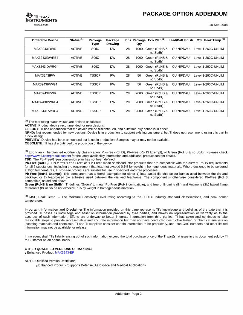
PACKAGING INFORMATION
Orderable Device Status (1) PackageType
PackageDrawing
Pins PackageQty
Eco Plan (2) Lead/Ball Finish MSL Peak Temp (3)
MAX3243CDB ACTIVE SSOP DB 28 50 Green (RoHS &no Sb/Br)
CU NIPDAU Level-1-260C-UNLIM
MAX3243CDBE4 ACTIVE SSOP DB 28 50 Green (RoHS &no Sb/Br)
CU NIPDAU Level-1-260C-UNLIM
MAX3243CDBG4 ACTIVE SSOP DB 28 50 Green (RoHS &no Sb/Br)
CU NIPDAU Level-1-260C-UNLIM
MAX3243CDBR ACTIVE SSOP DB 28 2000 Green (RoHS &no Sb/Br)
CU NIPDAU Level-1-260C-UNLIM
MAX3243CDBRE4 ACTIVE SSOP DB 28 2000 Green (RoHS &no Sb/Br)
CU NIPDAU Level-1-260C-UNLIM
MAX3243CDBRG4 ACTIVE SSOP DB 28 2000 Green (RoHS &no Sb/Br)
CU NIPDAU Level-1-260C-UNLIM
MAX3243CDW ACTIVE SOIC DW 28 20 Green (RoHS &no Sb/Br)
CU NIPDAU Level-1-260C-UNLIM
MAX3243CDWE4 ACTIVE SOIC DW 28 20 Green (RoHS &no Sb/Br)
CU NIPDAU Level-1-260C-UNLIM
MAX3243CDWG4 ACTIVE SOIC DW 28 20 Green (RoHS &no Sb/Br)
CU NIPDAU Level-1-260C-UNLIM
MAX3243CDWR ACTIVE SOIC DW 28 1000 Green (RoHS &no Sb/Br)
CU NIPDAU Level-1-260C-UNLIM
MAX3243CDWRG4 ACTIVE SOIC DW 28 1000 Green (RoHS &no Sb/Br)
CU NIPDAU Level-1-260C-UNLIM
MAX3243CPW ACTIVE TSSOP PW 28 50 Green (RoHS &no Sb/Br)
CU NIPDAU Level-1-260C-UNLIM
MAX3243CPWE4 ACTIVE TSSOP PW 28 50 Green (RoHS &no Sb/Br)
CU NIPDAU Level-1-260C-UNLIM
MAX3243CPWG4 ACTIVE TSSOP PW 28 50 Green (RoHS &no Sb/Br)
CU NIPDAU Level-1-260C-UNLIM
MAX3243CPWR ACTIVE TSSOP PW 28 2000 Green (RoHS &no Sb/Br)
CU NIPDAU Level-1-260C-UNLIM
MAX3243CPWRE4 ACTIVE TSSOP PW 28 2000 Green (RoHS &no Sb/Br)
CU NIPDAU Level-1-260C-UNLIM
MAX3243CPWRG4 ACTIVE TSSOP PW 28 2000 Green (RoHS &no Sb/Br)
CU NIPDAU Level-1-260C-UNLIM
MAX3243IDB ACTIVE SSOP DB 28 50 Green (RoHS &no Sb/Br)
CU NIPDAU Level-1-260C-UNLIM
MAX3243IDBE4 ACTIVE SSOP DB 28 50 Green (RoHS &no Sb/Br)
CU NIPDAU Level-1-260C-UNLIM
MAX3243IDBG4 ACTIVE SSOP DB 28 50 Green (RoHS &no Sb/Br)
CU NIPDAU Level-1-260C-UNLIM
MAX3243IDBR ACTIVE SSOP DB 28 2000 Green (RoHS &no Sb/Br)
CU NIPDAU Level-1-260C-UNLIM
MAX3243IDBRE4 ACTIVE SSOP DB 28 2000 Green (RoHS &no Sb/Br)
CU NIPDAU Level-1-260C-UNLIM
MAX3243IDBRG4 ACTIVE SSOP DB 28 2000 Green (RoHS &no Sb/Br)
CU NIPDAU Level-1-260C-UNLIM
MAX3243IDW ACTIVE SOIC DW 28 20 Green (RoHS &no Sb/Br)
CU NIPDAU Level-1-260C-UNLIM
MAX3243IDWG4 ACTIVE SOIC DW 28 20 Green (RoHS &no Sb/Br)
CU NIPDAU Level-1-260C-UNLIM
PACKAGE OPTION ADDENDUM
www.ti.com 18-Sep-2008
Addendum-Page 1
Orderable Device Status (1) PackageType
PackageDrawing
Pins PackageQty
Eco Plan (2) Lead/Ball Finish MSL Peak Temp (3)
MAX3243IDWR ACTIVE SOIC DW 28 1000 Green (RoHS &no Sb/Br)
CU NIPDAU Level-1-260C-UNLIM
MAX3243IDWRE4 ACTIVE SOIC DW 28 1000 Green (RoHS &no Sb/Br)
CU NIPDAU Level-1-260C-UNLIM
MAX3243IDWRG4 ACTIVE SOIC DW 28 1000 Green (RoHS &no Sb/Br)
CU NIPDAU Level-1-260C-UNLIM
MAX3243IPW ACTIVE TSSOP PW 28 50 Green (RoHS &no Sb/Br)
CU NIPDAU Level-1-260C-UNLIM
MAX3243IPWG4 ACTIVE TSSOP PW 28 50 Green (RoHS &no Sb/Br)
CU NIPDAU Level-1-260C-UNLIM
MAX3243IPWR ACTIVE TSSOP PW 28 2000 Green (RoHS &no Sb/Br)
CU NIPDAU Level-1-260C-UNLIM
MAX3243IPWRE4 ACTIVE TSSOP PW 28 2000 Green (RoHS &no Sb/Br)
CU NIPDAU Level-1-260C-UNLIM
MAX3243IPWRG4 ACTIVE TSSOP PW 28 2000 Green (RoHS &no Sb/Br)
CU NIPDAU Level-1-260C-UNLIM
(1) The marketing status values are defined as follows:ACTIVE: Product device recommended for new designs.LIFEBUY: TI has announced that the device will be discontinued, and a lifetime-buy period is in effect.NRND: Not recommended for new designs. Device is in production to support existing customers, but TI does not recommend using this part ina new design.PREVIEW: Device has been announced but is not in production. Samples may or may not be available.OBSOLETE: TI has discontinued the production of the device.
(2) Eco Plan - The planned eco-friendly classification: Pb-Free (RoHS), Pb-Free (RoHS Exempt), or Green (RoHS & no Sb/Br) - please checkhttp://www.ti.com/productcontent for the latest availability information and additional product content details.TBD: The Pb-Free/Green conversion plan has not been defined.Pb-Free (RoHS): TI's terms "Lead-Free" or "Pb-Free" mean semiconductor products that are compatible with the current RoHS requirementsfor all 6 substances, including the requirement that lead not exceed 0.1% by weight in homogeneous materials. Where designed to be solderedat high temperatures, TI Pb-Free products are suitable for use in specified lead-free processes.Pb-Free (RoHS Exempt): This component has a RoHS exemption for either 1) lead-based flip-chip solder bumps used between the die andpackage, or 2) lead-based die adhesive used between the die and leadframe. The component is otherwise considered Pb-Free (RoHScompatible) as defined above.Green (RoHS & no Sb/Br): TI defines "Green" to mean Pb-Free (RoHS compatible), and free of Bromine (Br) and Antimony (Sb) based flameretardants (Br or Sb do not exceed 0.1% by weight in homogeneous material)
(3) MSL, Peak Temp. -- The Moisture Sensitivity Level rating according to the JEDEC industry standard classifications, and peak soldertemperature.
Important Information and Disclaimer:The information provided on this page represents TI's knowledge and belief as of the date that it isprovided. TI bases its knowledge and belief on information provided by third parties, and makes no representation or warranty as to theaccuracy of such information. Efforts are underway to better integrate information from third parties. TI has taken and continues to takereasonable steps to provide representative and accurate information but may not have conducted destructive testing or chemical analysis onincoming materials and chemicals. TI and TI suppliers consider certain information to be proprietary, and thus CAS numbers and other limitedinformation may not be available for release.
In no event shall TI's liability arising out of such information exceed the total purchase price of the TI part(s) at issue in this document sold by TIto Customer on an annual basis.
OTHER QUALIFIED VERSIONS OF MAX3243 :
• Enhanced Product: MAX3243-EP
NOTE: Qualified Version Definitions:
• Enhanced Product - Supports Defense, Aerospace and Medical Applications
PACKAGE OPTION ADDENDUM
www.ti.com 18-Sep-2008
Addendum-Page 2

TAPE AND REEL INFORMATION
*All dimensions are nominal
Device PackageType
PackageDrawing
Pins SPQ ReelDiameter
(mm)
ReelWidth
W1 (mm)
A0 (mm) B0 (mm) K0 (mm) P1(mm)
W(mm)
Pin1Quadrant
MAX3243CDBR SSOP DB 28 2000 330.0 16.4 8.2 10.5 2.5 12.0 16.0 Q1
MAX3243CDWR SOIC DW 28 1000 330.0 32.4 11.35 18.67 3.1 16.0 32.0 Q1
MAX3243CPWR TSSOP PW 28 2000 330.0 16.4 6.9 10.2 1.8 12.0 16.0 Q1
MAX3243CPWR TSSOP PW 28 2000 330.0 16.4 7.1 10.4 1.6 12.0 16.0 Q1
MAX3243IDBR SSOP DB 28 2000 330.0 16.4 8.2 10.5 2.5 12.0 16.0 Q1
MAX3243IDWR SOIC DW 28 1000 330.0 32.4 11.35 18.67 3.1 16.0 32.0 Q1
MAX3243IPWR TSSOP PW 28 2000 330.0 16.4 7.1 10.4 1.6 12.0 16.0 Q1
MAX3243IPWR TSSOP PW 28 2000 330.0 16.4 6.9 10.2 1.8 12.0 16.0 Q1
PACKAGE MATERIALS INFORMATION
www.ti.com 18-Sep-2008
Pack Materials-Page 1

*All dimensions are nominal
Device Package Type Package Drawing Pins SPQ Length (mm) Width (mm) Height (mm)
MAX3243CDBR SSOP DB 28 2000 346.0 346.0 33.0
MAX3243CDWR SOIC DW 28 1000 346.0 346.0 49.0
MAX3243CPWR TSSOP PW 28 2000 346.0 346.0 33.0
MAX3243CPWR TSSOP PW 28 2000 346.0 346.0 33.0
MAX3243IDBR SSOP DB 28 2000 346.0 346.0 33.0
MAX3243IDWR SOIC DW 28 1000 346.0 346.0 49.0
MAX3243IPWR TSSOP PW 28 2000 346.0 346.0 33.0
MAX3243IPWR TSSOP PW 28 2000 346.0 346.0 33.0
PACKAGE MATERIALS INFORMATION
www.ti.com 18-Sep-2008
Pack Materials-Page 2
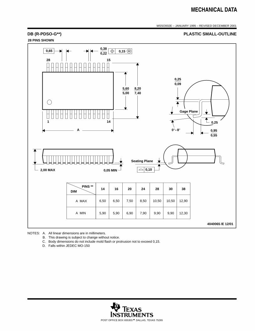
MECHANICAL DATA
MSSO002E – JANUARY 1995 – REVISED DECEMBER 2001
POST OFFICE BOX 655303 • DALLAS, TEXAS 75265
DB (R-PDSO-G**) PLASTIC SMALL-OUTLINE
4040065 /E 12/01
28 PINS SHOWN
Gage Plane
8,207,40
0,550,95
0,25
38
12,90
12,30
28
10,50
24
8,50
Seating Plane
9,907,90
30
10,50
9,90
0,38
5,605,00
15
0,22
14
A
28
1
2016
6,506,50
14
0,05 MIN
5,905,90
DIM
A MAX
A MIN
PINS **
2,00 MAX
6,90
7,50
0,65 M0,15
0°–8°
0,10
0,090,25
NOTES: A. All linear dimensions are in millimeters.B. This drawing is subject to change without notice.C. Body dimensions do not include mold flash or protrusion not to exceed 0,15.D. Falls within JEDEC MO-150

MECHANICAL DATA
MTSS001C – JANUARY 1995 – REVISED FEBRUARY 1999
POST OFFICE BOX 655303 • DALLAS, TEXAS 75265
PW (R-PDSO-G**) PLASTIC SMALL-OUTLINE PACKAGE14 PINS SHOWN
0,65 M0,10
0,10
0,25
0,500,75
0,15 NOM
Gage Plane
28
9,80
9,60
24
7,90
7,70
2016
6,60
6,40
4040064/F 01/97
0,30
6,606,20
8
0,19
4,304,50
7
0,15
14
A
1
1,20 MAX
14
5,10
4,90
8
3,10
2,90
A MAX
A MIN
DIMPINS **
0,05
4,90
5,10
Seating Plane
0°–8°
NOTES: A. All linear dimensions are in millimeters.B. This drawing is subject to change without notice.C. Body dimensions do not include mold flash or protrusion not to exceed 0,15.D. Falls within JEDEC MO-153


IMPORTANT NOTICETexas Instruments Incorporated and its subsidiaries (TI) reserve the right to make corrections, modifications, enhancements, improvements,and other changes to its products and services at any time and to discontinue any product or service without notice. Customers shouldobtain the latest relevant information before placing orders and should verify that such information is current and complete. All products aresold subject to TI’s terms and conditions of sale supplied at the time of order acknowledgment.TI warrants performance of its hardware products to the specifications applicable at the time of sale in accordance with TI’s standardwarranty. Testing and other quality control techniques are used to the extent TI deems necessary to support this warranty. Except wheremandated by government requirements, testing of all parameters of each product is not necessarily performed.TI assumes no liability for applications assistance or customer product design. Customers are responsible for their products andapplications using TI components. To minimize the risks associated with customer products and applications, customers should provideadequate design and operating safeguards.TI does not warrant or represent that any license, either express or implied, is granted under any TI patent right, copyright, mask work right,or other TI intellectual property right relating to any combination, machine, or process in which TI products or services are used. Informationpublished by TI regarding third-party products or services does not constitute a license from TI to use such products or services or awarranty or endorsement thereof. Use of such information may require a license from a third party under the patents or other intellectualproperty of the third party, or a license from TI under the patents or other intellectual property of TI.Reproduction of TI information in TI data books or data sheets is permissible only if reproduction is without alteration and is accompaniedby all associated warranties, conditions, limitations, and notices. Reproduction of this information with alteration is an unfair and deceptivebusiness practice. TI is not responsible or liable for such altered documentation. Information of third parties may be subject to additionalrestrictions.Resale of TI products or services with statements different from or beyond the parameters stated by TI for that product or service voids allexpress and any implied warranties for the associated TI product or service and is an unfair and deceptive business practice. TI is notresponsible or liable for any such statements.TI products are not authorized for use in safety-critical applications (such as life support) where a failure of the TI product would reasonablybe expected to cause severe personal injury or death, unless officers of the parties have executed an agreement specifically governingsuch use. Buyers represent that they have all necessary expertise in the safety and regulatory ramifications of their applications, andacknowledge and agree that they are solely responsible for all legal, regulatory and safety-related requirements concerning their productsand any use of TI products in such safety-critical applications, notwithstanding any applications-related information or support that may beprovided by TI. Further, Buyers must fully indemnify TI and its representatives against any damages arising out of the use of TI products insuch safety-critical applications.TI products are neither designed nor intended for use in military/aerospace applications or environments unless the TI products arespecifically designated by TI as military-grade or "enhanced plastic." Only products designated by TI as military-grade meet militaryspecifications. Buyers acknowledge and agree that any such use of TI products which TI has not designated as military-grade is solely atthe Buyer's risk, and that they are solely responsible for compliance with all legal and regulatory requirements in connection with such use.TI products are neither designed nor intended for use in automotive applications or environments unless the specific TI products aredesignated by TI as compliant with ISO/TS 16949 requirements. Buyers acknowledge and agree that, if they use any non-designatedproducts in automotive applications, TI will not be responsible for any failure to meet such requirements.Following are URLs where you can obtain information on other Texas Instruments products and application solutions:Products ApplicationsAmplifiers amplifier.ti.com Audio www.ti.com/audioData Converters dataconverter.ti.com Automotive www.ti.com/automotiveDSP dsp.ti.com Broadband www.ti.com/broadbandClocks and Timers www.ti.com/clocks Digital Control www.ti.com/digitalcontrolInterface interface.ti.com Medical www.ti.com/medicalLogic logic.ti.com Military www.ti.com/militaryPower Mgmt power.ti.com Optical Networking www.ti.com/opticalnetworkMicrocontrollers microcontroller.ti.com Security www.ti.com/securityRFID www.ti-rfid.com Telephony www.ti.com/telephonyRF/IF and ZigBee® Solutions www.ti.com/lprf Video & Imaging www.ti.com/video
Wireless www.ti.com/wireless
Mailing Address: Texas Instruments, Post Office Box 655303, Dallas, Texas 75265Copyright © 2008, Texas Instruments Incorporated