2dfun - 2d functional mx2/graphene hetero-structures · ieee 2001, d. esseni et al. ieee 2006,...
TRANSCRIPT

2DFUN - 2D FUNCTIONAL MX2/GRAPHENE HETERO-STRUCTURES
FLAG-ERA JTC 2015 PROJECT KICK-OFF APRIL 13, 2016, BUDAPEST, HUNGARY
MATTY CAYMAX, PROJECT COORDINATOR
www.2Dfun.eu

MATTY CAYMAX
2D MATERIALS – GRAPHENE AND BEYOND
2
VISION AND TIMELINE
Jari Kinaret, “Graphene Flagship”
presentation “ Working together to
combine scientific excellence and
technological impacts”, 2012

MATTY CAYMAX
WHY MX2 FOR TRANSISTOR
SCALING?
MX2: interesting properties for ultra-thin body devices
2D crystals with VdW bonding –no lattice mismatch issues
High DOS
Reasonable mobility, especially for ultra-thin channels
Low dielectric constant helps reducing short-channel effects (planar devices)
Wide band gap and wide choice of BGs allow BG engineering in TFET
Low density of dangling bonds on surface reduce defect density
3
MOSFET
1 10 10010
100
1000
10000
Mo
bilit
y [
cm
2/V
s]
Body Thickness [nm]
Sub-1nm Sub-10nm Bulk
Nature 2010, H. Ko et al.
IEDM 2013, A. Alian et al.
IEEE 2001, D. Esseni et al.
IEEE 2006, Tsutsui et al.
Nature Nanothech. 2010, Radisavljevic et al.Nano Lett. 2012,Wang et al.
InAs
Si
InGaAs
MoS2
TFET

MATTY CAYMAX
WHY GRAPHENE/MX2 HETERO-STRUCTURES?
4
Lee et al. ACS Nano DOI:
10.1021/acsnano.5b01341
Ohmic contacts between
MoS2 and Graphene
Challenge : long term
stability
2. Circuit scaling approach:
Electrolytic gating of a MoS2 flake shows ambipolar conduction
MoS2 is normally n-type
Smaller XOR can be built with 2 gate transistors
4 devices rather than 8 needed for same logic operation
Possible because of the ability to reconfigure the devices
3D scaling through stacking of devices possible
1. Contacts to MX2 are
bottleneck
Graphene/MX2
ohmic contacts
shown
Challenge is long-
term stability
Zhang et al. NanoLetters (2012)Graphene
L <100 nm
t <10 nm
Gateable contact to induce
ambipolarity N- or P-type

MATTY CAYMAX
CHALLENGES
Synthesis of high-quality 2D MX2 layers with controlled thickness on large wafer size (300mm) No reliable processes known/developed
No commercial reactors available
Growth of layers on saturated, passive 2D surfaces (graphene, MX2) Requires surface functionalization
Importance of interfaces: Interface between MoS2 and Gate dielectric: Effect on
mobility, hysteresis, reliability
Contact between MoS2 and graphene: Ohmic? Contact resistance?
Coping with high current densities?
Scaling potential?
MX2 MAKING AND DEVICE STRUCTURE
High-k dielectric
Dielectric
5

MATTY CAYMAX
2DFUN OBJECTIVES
Technological Objectives
1. Develop large-area deposition process for MX2 on graphene
1. Low-T sulfidation (plasma enhanced) of ALD-grown metal or metal oxide layers
2. Direct growth from gas phase (ALD, CVD) with M and X gas-phase precursors
2. Develop high-k dielectric growth process on MX2
Surface functionalization of graphene and MX2 for these growth processes
Scientific Objective:
1. Obtain fundamental insight in chemical structure and energy states spectrum at the high-
k/MX2 and MX2/graphene interfaces
6

MATTY CAYMAX 7
2DFUN PROJECT AND PROJECT LAY-OUT
WP2/T2.3
High-k/MX2/grapheneTLM, MOS cap
MOSFET
WP3
Physico-Chemical
Materials&Interfaces char
Electrical device
characterization
WP4
Graphene/MX2/high-k
Interfaces Spectroscopy and
Modeling
WP5 Project Management, dissemination & exploitation
WP2
High-k/MX2/graphene:T2.1 MX2 functionalization
T2.2High-k by ALD
WP1
MX2/graphene:1. Graphene
functionalization
2. MX2 by ALD and PE-
sulfurization
dielectric
High-k dielectric
MATTY CAYMAX
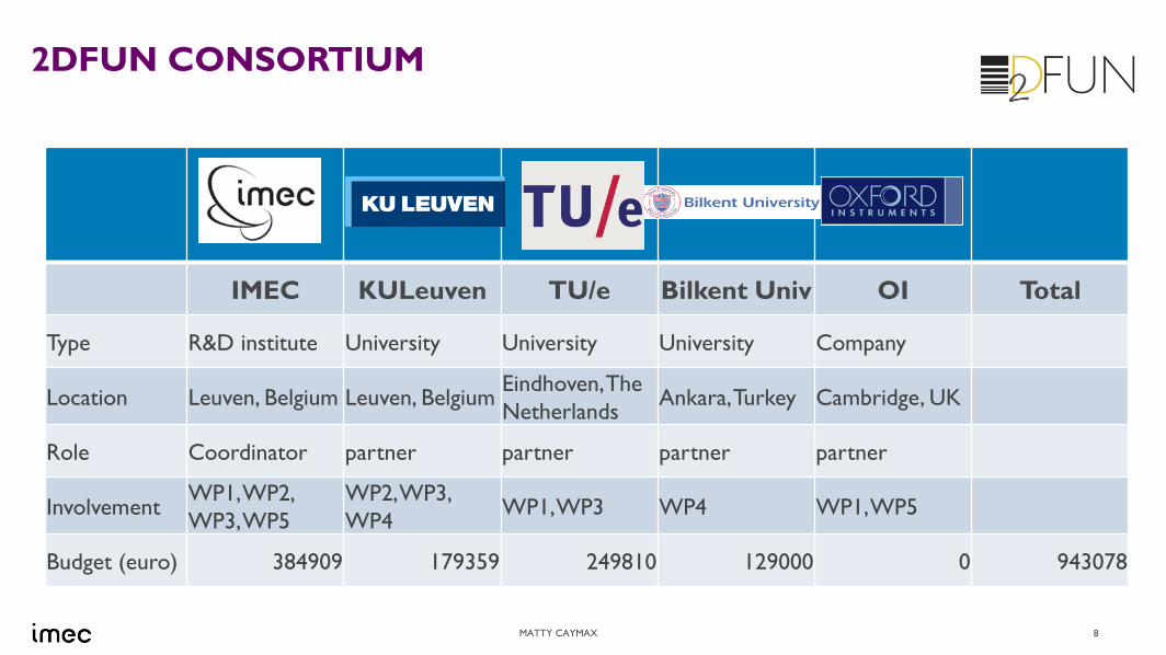
2DFUN CONSORTIUM
8
IMEC KULeuven TU/e Bilkent Univ OI Total
Type R&D institute University University University Company
Location Leuven, Belgium Leuven, BelgiumEindhoven, The
NetherlandsAnkara, Turkey Cambridge, UK
Role Coordinator partner partner partner partner
InvolvementWP1, WP2,
WP3, WP5
WP2, WP3,
WP4WP1, WP3 WP4 WP1, WP5
Budget (euro) 384909 179359 249810 129000 0 943078
MATTY CAYMAX
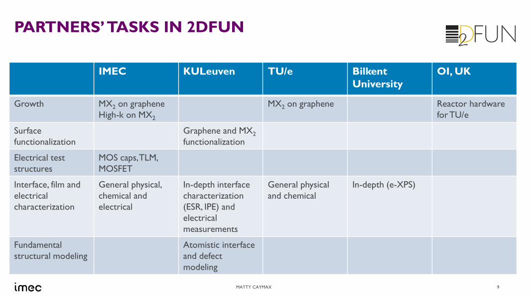
PARTNERS’ TASKS IN 2DFUN
IMEC KULeuven TU/e Bilkent
University
OI, UK
Growth MX2 on graphene
High-k on MX2
MX2 on graphene Reactor hardware
for TU/e
Surface
functionalization
Graphene and MX2
functionalization
Electrical test
structures
MOS caps, TLM,
MOSFET
Interface, film and
electrical
characterization
General physical,
chemical and
electrical
In-depth interface
characterization
(ESR, IPE) and
electrical
measurements
General physical
and chemical
In-depth (e-XPS)
Fundamental
structural modeling
Atomistic interface
and defect
modeling
9

MATTY CAYMAX
IMPACT
NRFO in Belgium:
VLAIO
Strong industrial link
via industrial partners:
ASM Belgium
AMAT Belgium
LAM Belgium
10
Large area
process high-k on
MX2
Low-T Plasma
Enhanced
Sulfidation
Electrical in-
depth
characterization
Ab-initio
modeling
Large area
process MX2 on
graphene
2D crystal
functionalization
Chemical-
structural
characterization
Electrical test-
structure and
device making
Film processing
Device integration

MATTY CAYMAX
MX2 LAYER SPECIFICATIONS TO BE REACHED
Requirements Target Measurement technique
Uniformity 100- 300mm Si wafer scale Spectroscopic ellipsometry
Number of layers Controlled between 1-5 Raman, RBS; For a single layer: M
content= 1.2E+15 at/cm2
Composition W/S = ½ Rutherford Backscattering
Spectroscopy
Impurity content < 1 at% Elastic Recoil Detection, XPS
Crystallinity Monocrystalline, basal plane parallel
to the substrate surface
Domain size > 50µm2
GI-X-Ray Diffraction, Transmission
Electron Microscopy, Atomic Force
Microscopy, Photoluminescence
mapping
Layer continuity Normalized substrate intensity < 1% TOFSIMS
Contact resistance < 400 ohm.µm I/V measurement on TLM
Mobility 20 cm2/Vs Split CV in MOSFETs
11

MATTY CAYMAX
EXPLOITABLE RESULTS
12
TARGETED INDUSTRIALLY VIABLE PROJECT OUTCOMES
Exploitable result TRL at
project
start
TRL
target
Comment
Process for
manufacturable
sulphurization of
transition metal layer
3 5 Advancing from known post-process sulphurization of coupons to in
situ (no vacuum break) sulphurization of 300mm wafers
Process for growth of
MX2 layer on an ‘inert’
layer such as graphene
2 3 Advancing from no prior demonstration to success on (coupons
distributed over) a 300mm wafer
Process for growth of
high-k dielectric on MX2
layer
2 4 Advancing from no prior demonstration to results on 200 and/or
300mm wafers
Manufacturing process
flow for a functional
MX2-based MOSFET
2 4 Advancing from results based on exfoliated layers to a lab-flow on
coupons
Process tool
specifications capable of
delivering the project
process advances
3 4 The project has only minor hardware developments, but will validate
the necessary features of process tools required to exploit these
methods

MATTY CAYMAX
DISSEMINATION OF RESULTS AND TRAINING
ACTIVITIES
Website hosted by imec: www.2Dfun.eu Public domain information only
Project description, consortium, members,...
Annual reports
Public deliverable reports
Partner publications, presentations...
Useful links
Presence on other websites FLAG-ERA website
Graphene Onboard Website of Graphene Flagship
Imec’s internal project website = restricted area for IWT SBO participants
Workshop(s) To be organized at/by imec as satellite event of imec PTW (April or October)
Publications & Conference presentations all partners
Papers & presentations posted on website
13

MATTY CAYMAX
INTERACTION WITH GRAPHENE FLAGSHIP
Complementarities WP3 - Enabling Materials
growth on large area substrates
in-depth fundamental understanding of the interfaces in 2D hetero-structures
WP8 - Photonics and Optoelectronics
direct bandgap in single layer MX2, as part of graphene/MX2 hetero-structures
WP9 - Flexible electronics
low-temperature growth techniques, without the need for transfer
WP10 - Wafer-Scale System Integration
CMOS compatible graphene processing modules for integration schemes which are scalable to sub 10nm dimensions on industrial wafer scale (300mm)
Foreseen interactions WP3 to provide various graphene samples to help benchmarking graphene/MX2 and MX2/high-k oxide stacks:
Graphene flakes for transfer onto Si substrate?
Graphene on Si substrate?
Natural or synthesized graphene?
WP3 to collaborate in the characterization of 2Dfun MX2/graphene samples
WP9 to look into possible use of the graphene/MX2/high k-oxide stacks for opto-electronic applications
14
MATTY CAYMAX
FIRST RESULTS
WP1&2 - KULeuven chemistry dpt, TU/e and imec: functionalization of graphene, high-growth on 2D materials
A suitable molecule for graphene functionalization was identified, and its thermal stability studied.
First Al2O3 layer growth on functionalized graphene by thermal ALD shown to result in nicely closed and smooth layers
WP1 – TU/e: MoS2 growth by thermal sulfidation of ALD-grown MoO3 shown, as first step towards full PE-sulfidation of same MoO3 layers
WP4 – KULeuven Physics dpt:
IPE study of WS2 and MoS2 on SiO2 shows that the valence band tops of both sulfides are very well aligned, hence the “Common anion” rule is valid for MX2 compounds
DFT calculations on a 1ML MoS2 film
show how the structures of S and Mo vacancies as well as S and Mo antisites in look like
Allow to calculate the g-factor of the same defects
