2d-nanolattices - cordis · 2017-04-20 · 2d nanolattices project to explore silicene as a new...
TRANSCRIPT
1
2D-NANOLATTICES FP7-ICT-2009-C (FET Open)
Highly anisotropic graphite-like semiconductor/dielectric
2D nanolattices
Deliverable D5.1
Dissemination and Use Plan
Report
Prepared by Dr. A. Dimoulas
Contributors: All
Preparation Date: 28/06/2013
Report version number: final
Classification: Public
Contract Start Date: 01/06/2011
Duration: 36 months
Project Coordinator: NCSR- D (Dr. A. Dimoulas)
Contractors: IMEC, KULeuven, CNR, CNRS, U. de Provence
Project funded by the European Community under the
“Future and Emerging Technologies” Programme
2
Table of Contents
Part A: Dissemination...................................................................................................................... 3
A.1 Publications in International Journals................................................................................... 4
A.2 Conferences and Invited Presentations................................................................................ 5
A.3 Workshop Conferences organization ................................................................................. 12
A.4 Press release ....................................................................................................................... 12
YOUR NEWS ...................................................................................................................... 12
Silicene: a new "fabric" for nanoelectronics made of the same raw material, silicon ...................................................................................................................................... 12
Technology News ...................................................................................................................... 15
2D Nanolattices project to explore Silicene as a new “fabric” for nanoelectronics .................... 15
A.5 Networking in the European Research Area....................................................................... 17
A.6 Web..................................................................................................................................... 17
Part B: Use of results..................................................................................................................... 19
B.1. Identification of exploitable results ................................................................................... 19
B.2 Plan for exploitation............................................................................................................ 19
3
This deliverable will be updated periodically as described in the Gantt chart in ANNEX I/DoW. Due to the short time elapsed from the start of the project, the first version of D5.1 contains very few actual dissemination actions, while most of the material presented here concerns plans for dissemination and use targeting the first 18 months.
Part A: Dissemination
A.1 Research Highlights
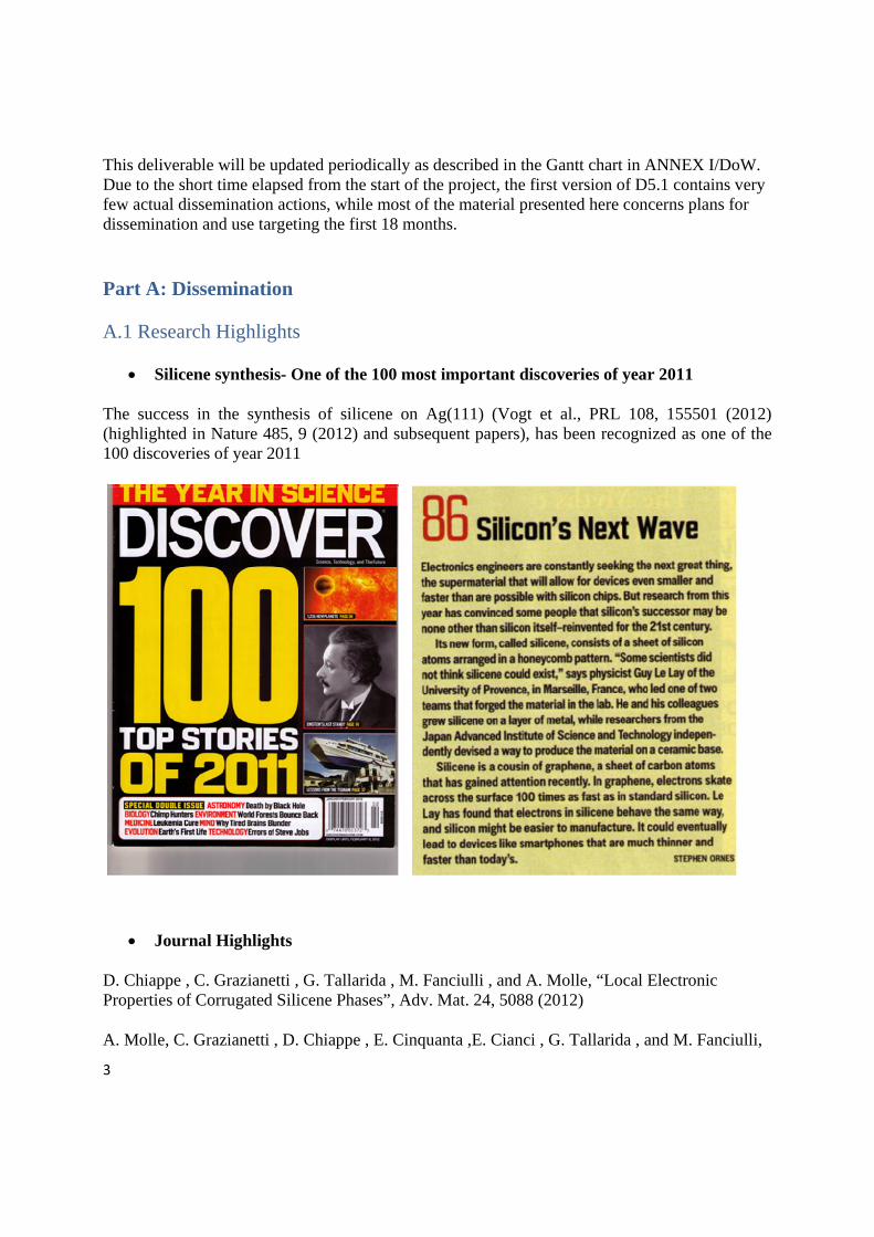
Silicene synthesis- One of the 100 most important discoveries of year 2011
The success in the synthesis of silicene on Ag(111) (Vogt et al., PRL 108, 155501 (2012) (highlighted in Nature 485, 9 (2012) and subsequent papers), has been recognized as one of the 100 discoveries of year 2011
Journal Highlights
D. Chiappe , C. Grazianetti , G. Tallarida , M. Fanciulli , and A. Molle, “Local Electronic Properties of Corrugated Silicene Phases”, Adv. Mat. 24, 5088 (2012)
A. Molle, C. Grazianetti , D. Chiappe , E. Cinquanta ,E. Cianci , G. Tallarida , and M. Fanciulli,
4
“Hindering the Oxidation of Silicene with Non-Reactive Encapsulation”, Adv. Funct. Mat. DOI: 10.1002/adfm.201300354
A.2 Publications in International Journals
We give below 2D-NANOLATTICES member publications or articles in preparation which are relevant to the 2D-NANOLATTICES research topics.
a) First reporting period
i) Already published/accepted
E. Scalise, M. Houssa, V.V. Afanas'ev and A. Stesmans, “Strain-induced semiconductor to metal transition in the two-dimensional honeycomb structure of MoS2”, Nano Research 5, 43 (2012). P. Vogt, P. de Padova, C. Quaresima, J. Avila, E. Franzeskakis, M. C. Asensio, A. Resta, B. Ealet and G. Le Lay, “Silicene: Compelling Experimental Evidence for Graphene like Two-Dimensional Silicon”, PRL 108, 155501 (2012).
b) Second reporting period
i) Planned/in preparation E. Golias, E. Xenogiannopoulou, D. Tsoutsou, P. Tsipas, S. A. Giamini, A. Dimoulas, “Surface electronic bands of sub-monolayer Ge on Ag(111)”, submitted to PRB. E. Golias, E. Xenogiannopoulou, D. Tsoutsou, P. Tsipas, S. A. Giamini, A. Dimoulas, “A lab-based ARPES investigation of silicene nanosheets grown on Ag(111)”, should be submitted to APL in August 2013. M. Houssa et al, 3 papers are planned to be submitted to Applied Surface Sciences (EMRS proceedings), one to Phys. Chem. Chem. Phys, one to J. New Phys.
ii) Already published/accepted E. Scalise, M. Houssa, G. Pourtois, V.V. Afanas’ev and A. Stesmans, “First-principles study of strained 2D MoS2”, Physica E, accepted 10 July 2012, in press. P. De Padova, P. Vogt, A. Resta, J. Avila, I. Razado-Colambo, C. Quaresima, C. Ottaviani, B. Olivieri, T., T. Hirahara, T. Shirai, S. Hasegawa, M. C. Asensio, and G. Le Lay, “Evidence of Dirac fermions in multilayer silicene”, Appl. Phys. Lett. 102, 163106 (2013) J. Avila, P. De Padova, S. Cho, I. Colambo, S. Lorcy, C. Quaresima, P. Vogt, A. Resta, G. Le Lay and M.-C. Asensio, J. Phys.: Condens. Matter 25 262001 (2013).

5
M. Houssa, B. van den Broek, E. Scalise, G. Pourtois, V. V. Afanas'ev and A. Stesmans , “An electric field tunable energy band gap at silicene/(0001) ZnS interfaces”, Phys. Chem. Chem. Phys. 15, 3702 (2013). A. Molle, C. Grazianetti, D. Chiappe, E. Cinquanta, E. Cianci, G. Tallarida and M. Fanciulli, “Hindering the Oxidation of Silicene with Non-Reactive Encapsulation”, Adv. Fun. Mater. published online: 9 April 2013. E. Scalise, M. Houssa, G Pourtois, B. van den Broek, V. Afanas’ev, and A Stesmans, “Vibrational properties of silicene and germanene”, Nano Research, 6, 19-28 (2013). P. De Padova, O. Kubo, B. Olivieri, C. Quaresima, T. Nakayama, M. Aono, and G. Le Lay, “Multilayer Silicene Nanoribbons”, Nano Lett., 12 (11), 5500 (2012). D. Chiappe, C. Grazianetti, G. Tallarida, M. Fanciulli, and A. Molle, “Local Electronic Properties of Corrugated Silicene Phases”, Adv. Mater. 24, 5088 (2012). D. Kaltsas, L. Tsetseris and A. Dimoulas, “Structural evolution of single-layer films during deposition of silicon on silver: a first-principles study”, J. Phys.: Condens. Matter 24, 442001 (2012). G. Le Lay, P. De Padova, A. Resta, T. Bruhn and P. Vogt, “Epitaxial silicene: can it be strongly strained?”, J. Phys. D: Appl. Phys. 45 392001 (2012)
c) Third reporting period To be completed in due time, at the end of third period
A.2 Conferences and Invited Presentations
1) First reporting period
Guy Le Lay: Invited presentation Japan-UK workshop on Graphene Synthesis and Characterisation for Applications Workshop , Windermere lake, UK, Nov. 15-18, www.lancs.ac.uk/depts/esqn/WindermereWorkshop/ “Silicene: Dirac fermions in atom-thin epitaxial honeycomb silicon Sheets”
Guy Le Lay: Oral presentation “ Silicene epitaxial sheets” with P. Vogt, P. De Padova, C. Quaresima, J. Avila, E. Frantzeskakis, M.C. Asensio,B. Ealet AVS 58th Int. Symposium, Nashville, Tn, USA, Oct. 30 – Nov. 4, 2011 Guy Le Lay, Oral presentation “Epitaxial silicene sheets” with P. Vogt, P. De Padova, C. Quaresima, J. Avila, E. Frantzeskakis, M.C. Asensio, NANOSMAT, Krakow, Poland, October 17-20, 2011
6
Patrick Vogt, oral presentation “Formation of 2D hexagonal silicon monolayers on Ag(111): a graphene-like structure” with P. De Padova, M. E. Davila, M. Cei, A. Pietsch, F. Hennies and G. Le Lay at the Int. Conf. on the Formation of Semiconductor Interfaces (ICFSI-13), Prague, Czech Republic, July 3-8, 2011
Patrick Vogt, oral presentation “Formation of 2D hexagonal silicon monolayers on Ag(111): a graphene-like structure” with P. De Padova, M. E. Davila, M. Cei, A. Pietsch, F. Hennies and G. Le Lay at the European Conference On Surface Science (ECOSS-28) Wroclaw, Poland Aug. 28-Sept. 2, 2011
Guy Le Lay, invited talk “Silicene and prospects for other graphene-like nano-lattices” at the Int. Conf. on the Formation of Semiconductor Interfaces (ICFSI-13), Prague, Czech Republic, July 3-8, 2011
Paola De Padova oral presentation “Electronic structure of honeycomb silicon sheets on silver (111)” with P. Vogt, C. Quaresima, B. Olivieri and G. Le Lay at the 11th International Conference on Atomically Controlled Surfaces, Interfaces and Nanostructures October 3-7, 2011 St. Petersburg, Russia
Patrick Vogt invited talk “Honeycomb 2D silicon monolayers on Ag(111): a possible formation of silicene” with P. De Padova and G. Le Lay at Optics of Surfaces and Interfaces (OSI-9) Akumal, Mexico, Sept. 19-23, 2011 M. Houssa, E. Scalise, K. Sankaran, G. Pourtois, V.V. Afanas'ev, and A. Stesmans, “Hydrogenated silicene and germanene: A first-principles study”, presented at the 7th International Conference on Si Epitaxy and Heterostructures (Leuven, September 2011). A. Molle, oral presentation “Electronic structure and chemical reactivity of atomically thin silicon nanosheets with hexagonal symmetry epitaxially grown on Ag(111) surfaces” with D. Chiappe, C. Grazianetti, G. Tallarida, M. Fanciulli at the E-MRS 2012 Spring Meeting, Strasbourg, France, 14th-18th May 2012
2) Second reporting period
Presented:
A. Dimoulas, oral presentation “Graphene-like two-dimensional silicon and germanium structures on silver” with E. Golias, D. Tsoutsou, D. Kaltsas, E. Xenogianopoulou, P. Tsipas, S. Giamini, and L. Tsetseris at the Fifth International Conference "Micro&Nano2012" on Micro -
7
Nanoelectronics, Nanotechnologies and MEMS, 7-10 October 2012, Aquis Arina Sand Hotel, Kokkini Hani, Heraklion, Greece
A. Dimoulas, oral presentation “Search for graphene-like silicon and germanium 2D lattices” with D. Tsoutsou, E. Golias, D. Kaltsas, L. Tsetseris, B. Ealet and G. Le Lay at GrapHEL Conference, 27-30 September 2012, Mykonos, Greece
D. Tsoutsou, oral presentation “Search for sp2 hybridized graphene-like silicon and germanium layers grown on metal substrates” E. Golias, E. Xenogiannopoulou, P. Tsipas, N. Kelaidis and A. Dimoulas at the XXVIII Panhellenic Conference on Solid State Physics and Materials Science, 23-26 September 2012, Patras, Greece
A. Dimoulas, oral presentation “Surface band topology of Ge on Ag(111)” with E. Golias , E. Xenogiannopoulou , D. Tsoutsou , P. Tsipas , S. Giamini at the APS March Meeting 2013, March 18–22, 2013; Baltimore, Maryland, USA
E. Xenogiannopoulou, oral presentation “Silicon and Germanium atomically thin layers grown on metallic single crystals” with E. Golias , D. Tsoutsou , P. Tsipas , S. Giamini at the EMRS 2013 Spring Meeting,May 27-31, Strasbourg France
P. Tsipas, oral presentation “Graphite-like AlN templates and Si and Ge overgrowth” with S. Kassavetis, D. Tsoutsou, E. Golias, S. A. Giamini, E. Xenogiannopoulou, and A. Dimoulas at the EMRS 2013 Spring Meeting,May 27-31, Strasbourg France
C. Grazianetti, poster presentation “Silicon In situ characterization of silicon nanosheets grown on Ag(111)” with D. Chiappe, G. Tallarida, M. Fanciulli, A. Molle at the International Conference on Nanoscience + Technology (ICN+T2012) - July 23-27, 2012, Paris, France
D. Chiappe, oral presentation “Silicene: a new crystalline form of silicon” with C. Grazianetti, G. Tallarida, M. Fanciulli, A. Molle, G. Le Lay at the International Conference on Nanoscience + Technology (ICN+T2012) - July 23-27, 2012, Paris, France
E. Cinquanta et al, oral presentation “Raman spectrum of epitaxial silicene” at the MRS 2013 Spring Meeting, April 2013, San Francisco (USA)
D. Chiappe et al, poster presentation “In situ characterization of epitaxial silicene” at the MRS 2013 Spring Meeting, April 2013, San Francisco (USA)
C. Grazianetti et al, oral presentation “Morphological and electronic properties of silicene grown on Ag(111)” at the E-MRS 2013 Spring Meeting, May 27-31, 2013, Strasbourg (France)
C. Grazianetti et al, oral presentation “Hindering Oxidation of Silicene with Non-Reactive Encapsulation” at the E-MRS 2013 Spring Meeting, May 27-31, 2013, Strasbourg (France)

8
M. Caymax invited, ”Si/O Nano-lattices for engineered charge carrier mobility”, with S. Jayachandrana, A. Delabie, R. Loo, W. Vandervorst, M. Heyns, at the 6th International WorkShop on New Group IV Semiconductor Nanoelectronics, February 22-23, 2013, Sendai, Japan.
M. Caymax invited, “Oxygen in Si Epitaxial Growth: from Interface Contamination to Si/O Superlattice Engineering” with S. Jayachandran, Lu Augustin, A. Delabie, R. Loo, A. Hikavyy, G. Pourtois, W. Vandervorst, M. Heyns at the JSPS Core-to-Core Seminar on ‘Atomically Controlled Processing for Ultralarge Scale Integration’, June 6, 2013, Fukuoka, Japan.
A. Delabie oral presentation, “Chemical vapor deposition processes for the fabrication of epitaxial Si-O superlattices”, S. Jayachandran, M. Caymax, R. Loo, J. Maggen, J. Meersschaut, H. Lenka, W. Vandervorst, M. Heyns at the 8th international conference on silicon epitaxy and heterostructures (ICSI-8), June 2-5, 2013, Fukuoka, Japan
M. Houssa invited, ‘’Theoretical study of silicene and germanene’’, with B. van den Broek, E. Scalise, G. Pourtois, V.V. Afanas’ev, and A. Stesmans at the 223rd ECS Meeting, May 12-17 2013, Toronto, Canada
M. Houssa invited, ‘’Theoretical apsects of grapheme like group IV semiconductors’’, with B. van den Broek, E. Scalise, B. Ealet, G. Pourtois, D. Chiappe, E. Cinquanta, C. Grazianetti, M. Fanciulli, A. Molle, V.V. Afanas’ev, and A. Stesmans at the E-MRS Spring Meeting, May 27-31 2013, Strasbourg, France.
B. van den Broek oral presentation, ‘’Functionalization of silicene and germanene by chemisorption: an ab-initio study’’, with E. Scalise, G. Pourtois, M. Houssa, V.V. Afanas’ev, and A. Stesmans at the E-MRS Spring Meeting, May 27-31 2013, Strasbourg, France.
E. Scalise oral presentation, ‘’Theoretical study of silicene on non-metallic substrates with an hexagonal layered structure’’, with M. Houssa, B. van den Broek, E. Cinquanta, D. Chiappe, A. Molle, G. Pourtois, V.V. Afanas’ev, and A. Stesmans at the E-MRS Spring Meeting, May 27-31 2013, Strasbourg, France.
G. Le Lay invited, “Beyond Graphene: Silicene and Germanene Novel Electronic Materials” 2012 Si, SiGe & Related Compounds: Materials, Processing and Devices Symposium, Honolulu, Hawaii Oct. 7-12, 2012.
G. Le Lay invited, “The Dawn of Silicene” International Winterschool on Electronic Properties of Novel Materials, Kirchberg/Tirol, Austria, March 02-09, 2013.
G. Le Lay invited, “Silicene and Germanene Graphene’s close Relatives” Train2 Nanoscience International Conference Barcelona, Spain, November 22, 2012.
9
G. Le Lay invited, “Silicene, the silicon cousin of graphene” International Conference on Superstripes, Erice, Italy, July 11-17, 2012.
G. Le Lay invited, “Silicene: graphene’s topologically non-trivial cousin”, Physics ans Chemistry of Semiconductor Interfaces PCSI-40, Waikoloa, Hawaii, USA, Jan. 20-24, 2013.
A. Resta invited, “From Silicene Discovery to Graphene-Like Epitaxial Germanium Sheets”, DARPA workshop on 2D material, Pont A Mousson, France, September24-27, 2012.
A. Resta invited, “From Silicene Discovery to Graphene-Like Epitaxial Germanium Sheets”, International Conference of Young Researchers on Advanced Materials, Singapore, July 1-6, 2012.
P. Vogt and CNRS collaborators invited, “Formation of 2D Silicene on Ag(111): growth mode, atomic arrangements and Dirac Fermions”, NanoSea 2012, 25-29 June 2012, S. Margherita di Pula, Sardinia, Italy.
P. Vogt and CNRS collaborators invited, “Formation of silicene and 2D Si sheets on Ag(111): growth mode, structural and electronic properties”, XXI International Materials Research Congress, August 12 - 17, 2012, Cancun, Mexico.
P. Vogt and CNRS collaborators invited, “Silicene: a novel two-dimensional electronic material beyond graphene”, ANM 2012, 4th International Conference on Advanced Nano Materials, Chennai, India, Oct. 17-19, 2012.
P. Vogt and CNRS collaborators invited “Single- and multi-layer silicene: growth mode, structural and electronic Properties”, NanoMa Symposium, Chemnitz, Germany, Jan. 17, 2013.
P. Vogt and CNRS collaborators invited “Watch-out graphene, here comes Silicene! From epitaxial growth toward technological applicability”, ULIS 2013, Warwick, GB, March 19-22, 2013.
P. Vogt and CNRS collaborators invited “Epitaxial silicene”, E-MRS Spring Meeting, Strasburg, France, May 27-31.
G. Le Lay oral, “Single Layer to Multilayer Silicene: First Synthetic Graphene/Graphite-Like Material”, Granada’12, Granada, Spain, September 9-13, 2012.
G. Le Lay oral, “From Silicene Discovery to Graphene-like Epitaxial Germanium Sheets”, International Conference on Nanoscience + Technology (ICN+T2012) - July 23-27, 2012, Paris, France.
10
G. Le Lay oral, “From Epitaxial Silicene Sheets to the Quest for Majorana Fermions”, International Conference on Superconductivity and Magnetism, Istanbul, Turkey, April 29 – May 4, 2012.
G. Le Lay oral, “Silicene and Germanene Graphene’s Topologically Non-Trivial Cousins”, SICC-7, Singapore, Dec. 16-19, 2012.
G. Le Lay oral, “Atomic and Electronic Structures of Silicene Grown on Ag(111)”, E-MRS Spring Meeting, Strasbourg, France, May 26-30, 2013.
G. Le Lay oral, “Single Layer to Multilayer Silicene: First Synthetic Graphene/Graphite-Like Material”, TechConnect World 2013, National Innovation Summit, National Harbor, Maryland, USA, May 12-16, 2013.
A. Resta oral, “Silicene: first Combined non-Contact Atomic Force Microscopy and Scanning Tunnelling Microscopy Observations”, Physics Boat 2013, June 4-6, 2013, Helsinki, Finland - Stockholm, Sweden.
A. Resta oral, “From Silicene Discovery to Graphene-Like Epitaxial Germanium Sheets”, ICESS, Saint Malo, France, 16th-21st September 2012.
P. Vogt and CNRS collaborators oral “Structural and electronic properties of silicene layers on Ag(111)”, European Conference On Surface Science September 3- 7, 2012, Edinburgh, GB.
P. Vogt and CNRS collaborators oral “Formation of Silicene and 2D Si Sheets on Ag(111): Growth mode, Structural and Electronic Properties”, AVS 59th International Symposium, Tampa, Florida, USA, Oct. 28- Nov. 2, 2012.
Planned:
A. Dimoulas invited, “Growth and characterization of silicene and germanene”, 44th IEEE Semiconductor Interface Specialists Conference (SISC), December 5-7, 2013, Arlington, VA, Washington, DC
A. Molle, et al invited, "Structural and Chemical stabilization of epitaxial silicene", FLATLANDS BEYOND GRAPHENE Workshop, June 18-21, 2013, Bremen (Germany)
C. Grazianetti, et al poster presentation, "Hindering Oxidation of Silicene with Non-Reactive Encapsulation", FLATLANDS BEYOND GRAPHENE Workshop, June 18-21, 2013, Bremen (Germany)
11
D. Chiappe et al invited, "Structural and Chemical stabilization of silicene", CC3DMR 2013 Conference, June 24-28, 2013, Jeju Islands (Korea)
A. Molle, et al invited, "Silicene, an Option for Future Electronics", AVS Meeting, October 28-31, 2013, Los Angeles (USA)
A. Molle, et al invited, "Structural and Chemical stabilization of epitaxila silicene", ECS Meeting 29-31, San Francisco (USA)
M. Houssa oral presentation, ‘’Interaction of germanene with (0001)ZnSe surfaces: a theoretical study’’ with B. van den Broek, E. Scalise, G. Pourtois, V.V. Afanas’ev, and A. Stesmans to be presented at the 224 ECS Meeting, October 27-November 1 2013, San Francisco, USA.
G. Le Lay plenary invited, “"Silicene, the First Synthetic Graphene-like Material", 14th International Conference on the Formation of Semiconductor Interfaces, Gyeongju, Korea, June 30-July 5, 2013.
G. Le Lay plenary invited, 12th International Conference on Atomically Controlled Surfaces, Interfaces and Nanostructures, in conjunction with 21st International Colloquium on Scanning Probe Microscopy, November 4 - 8, 2013, Tsukuba International Congress Center, Tsukuba, Japan.
G. Le Lay invited, “Atomic resolution Imaging and Dirac Fermionics of Silicene Sheets”, The 1st WPI Workshop on Materials Science - The 10th France-Japan Workshop on Nanomaterials-Kyoto, Japan, June 6-9, 2013.
G. Le Lay invited, “Growth and properties of epitaxial single and multi-layer silicene”, The 19th American Conference on Crystal Growth and Epitaxy, July 21 - 26, 2013, Keystone, Colorado.
3) Third reporting period
To be completed in due time, at the end of third period
12
A.3 Workshop Conferences organization
1) First reporting period Planned: Following a proposal by Alessandro Molle of CNR, a symposium proposal for the EMRS 2013 in Strasbourg has been submitted. The symposium titled “The route to post CMOS devices: from high mobility channels to graphene-like 2D nanosheets” will emphasize 2D lattice structures like MoSe2, hexagonal BN, hexagonal Si and Ge, layered structures like Bi2Se3 and Bi2Te3 all with electronic structure and physical properties similar to graphene. The latter will also be included as one of the subtopics. As such, the symposium will be relevant to the 2D-NANOLATTICES themes and it will provide an opportunity to disseminate project results and enhance its visibility. 2D NANOLATTICES members, A. Molle (CNR), leading organizer, G. Le Lay (U.de Provence/CNRS) and A. Dimoulas (NCSRD) are in the organizing committee. Prof. Max Lemme (KTH) from the graphene community has been invited to participate in the committee. 2D-NANOLATTICES will sponsor the symposium from the coordinator’s management funds.
2) Second reporting period Organized: 2D-NANOLATTICES at the E-MRS 2013 Spring Meeting The EC - Future and Emerging Technologies project "2D-NANOLATTICES" sponsors the Symposium I: "Route to post-Si CMOS devices: from high mobility channels to graphene-like 2D nanosheets" at the E-MRS 2013 Spring Meeting. For more information please visit the Symposium I webpage.
Symposium Organizers: Alessandro Molle, CNR-IMM Laboratorio MDM Athanasios Dimoulas, NCSR DEMOKRITOS Guy Le Lay, CNRS-CINaM and Université de Provence Max Lemme, KTH Royal Institute of Technology,
A.4 Press release
We have published two press releases:
Press Release #1: Nanotechweb
http://nanotechweb.org/cws/article/yournews/46230
YOUR NEWS Jun 9, 2011
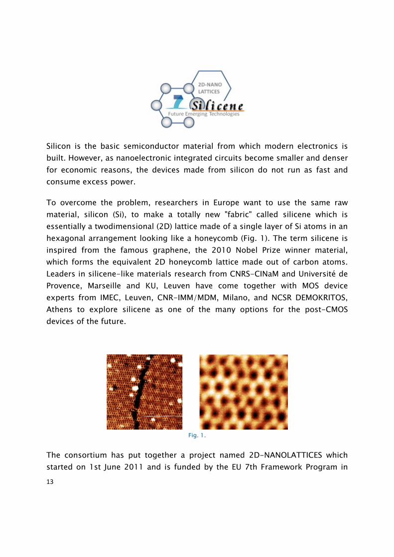
Silicene: a new "fabric" for nanoelectronics made of the same raw material, silicon
13
Silicon is the basic semiconductor material from which modern electronics is built. However, as nanoelectronic integrated circuits become smaller and denser for economic reasons, the devices made from silicon do not run as fast and consume excess power.
To overcome the problem, researchers in Europe want to use the same raw material, silicon (Si), to make a totally new "fabric" called silicene which is essentially a twodimensional (2D) lattice made of a single layer of Si atoms in an hexagonal arrangement looking like a honeycomb (Fig. 1). The term silicene is inspired from the famous graphene, the 2010 Nobel Prize winner material, which forms the equivalent 2D honeycomb lattice made out of carbon atoms. Leaders in silicene-like materials research from CNRS-CINaM and Université de Provence, Marseille and KU, Leuven have come together with MOS device experts from IMEC, Leuven, CNR-IMM/MDM, Milano, and NCSR DEMOKRITOS, Athens to explore silicene as one of the many options for the post-CMOS devices of the future.
Fig. 1.
The consortium has put together a project named 2D-NANOLATTICES which started on 1st June 2011 and is funded by the EU 7th Framework Program in

14
Future and Emerging Technologies (FET). Coordinated by NCSR DEMOKRITOS, the team aims at showing in three years from now that it is possible to engineer silicene and that this new 2D Si allotrope has better properties than conventional bulk Si for field effect electronic devices.
Fig. 2.
The task is difficult because silicene, which does not exist in Nature, is not as easy to form as graphene for reasons which may be related to the larger Si atom size and the specifics of its electronic structure. However, it seems that silicene-like material can be engineered if suitable metal substrates are used. As many of us, humans, silicene has an intimate relation with silver (Ag). Professor Guy Le Lay, a 2DNANOLATTICES consortium member and his coworkers, have obtained strong evidence of silicene-like monolayer sheets grown on single crystalline Ag (see Fig. 1), although it is not certain yet whether these layers form true silicene equivalent to graphene. One of the goals of the project is to unambiguously prove the existence of silicene and understand why Ag and possibly other metals are so “friendly” to it. On the other hand, metal substrates are not suitable for devices because they screen the electric fields and nullify field effects which are at the heart of the operation of present day electronic devices. Therefore, in 2DNANOLATTICES we will look for alternative substrates and capping layers with insulating properties to encapsulate silicene (Fig. 2). These insulating materials made for example from aluminum nitride are designed to be very similar to silicene in the way atoms bond to each other to form layered structures. Moreover, they will be bonded to silicene with weak van der Waals forces so that they can offer a “safe shelter” to silicene (Fig. 2) allowing electric charge to flow fast and undistracted in the plane as in the case of graphene.
15
The consortium members believe that the work in 2D-NANOLATTICES is not merely a replication of graphene properties with silicon instead of carbon atoms. The project goes beyond that exploring a number of other potential 2D nanolattices and their combinations to show that 2D materials beyond graphene can be created with potentially new properties for useful devices. The 2D world of nanolattices offers not only high speed but also a natural confinement of electronic transport in just one monolayer of lattice atoms, facilitating its manipulation in a very efficient way. This could make 2D nanolattices the ideal materials base for the future electronic devices offering high speed and low power /energy operation at the same time, the “holy grail” of nanoelectronics.
Source: Dr. Athanasios Dimoulas, 2D-NANOLATTICES project coordinator National Center for Scientific Research DEMOKRITOS Institute of Materials Science Patriarchou Grigoriou & Neapoleos 153 10, Athens, Greece Tel: +30 210 6503340 Fax: +30 210 6503377 e-mail: [email protected]
Press release #2: EE Times Europe http://www.electronics-eetimes.com/en/search.html?query=2D-NANOLATTICES
Technology News
2D Nanolattices project to explore Silicene as a new “fabric” for nanoelectronics
June 10, 2011 | Julien Happich | 222907789
16
Silicon is the basic semiconductor material from which modern electronics is
built. However, the same raw material could be used to build a totally new “fabric” called silicene,
essentially a two‐dimensional lattice made of a single layer of Si atoms arranged in a hexagonal
pattern very much like the atoms of carbon in graphene.
At a research stage, a two-dimensional, atom-thin silicon layer on a dense silver surface Ag(111) has been demonstrated at PCSI 2011, San Diego. The silicene layer exhibited a honeycomb arrangement like in graphene from which the new fabric's name has been inspired. Leaders in silicene-like materials research from CNRS-CINaM and Université de Provence, Marseille and KU Leuven have come together with MOS device experts from IMEC, Leuven, CNR-IMM/MDM, Agrate near Milano, and NCSR Demokritos, Athens to explore silicene as one of the future materials of electronics beyond CMOS devices.
The consortium has put together a project named 2D-Nanolattices, which started on the 1st of June 2011, funded by the EU 7th Framework Program in Future and Emerging Technologies (FET). Coordinated by NCSR Demokritos, the initial goal of this project is to examine the electronic properties of 2D Si lattices for field effect electronic devices and demonstrate the feasibility of silicene-based devices.
From the current state of research, it seems that silicene-like material can be engineered if suitable metal substrates are used such as silver. Yet, it is not sure whether these layers form a true silicene equivalent to graphene. One of the goals of the project is to unambiguously prove the existence of silicene and understand why Ag and possibly other metals are so “friendly” to it.
To circumvent the screening properties of metal substrates which nullify field effects, the 2D-Nanolattices project will look at alternative substrates and capping layers with insulating properties to encapsulate silicene. These insulating materials made for example from aluminum nitride are designed to be very similar to silicene in the way atoms bond to each other to form layered structures. Moreover, they will be bonded to silicene with weak van der Waals forces so that they can offer a “safe shelter” to silicone allowing electric charge to flow fast and undistracted in the plane as in the case of graphene.
The consortium members believe that the work in 2D-Nanolattices is not merely a replication of graphene properties with silicon instead of carbon atoms. The project goes beyond that exploring a number of other potential 2D nanolattices and their combinations to show that 2D materials beyond graphene can be created with potentially new properties for useful devices.
17
The 2D world of nanolattices offers not only high speed but also a natural confinement of electronic transport in just one monolayer of lattice atoms, facilitating its manipulation in a very efficient way. This could make 2D nanolattices the ideal materials base for the future electronic devices offering high speed and low power /energy operation at the same time.
A.5 Networking in the European Research Area
1) FET Flagship initiatives Our intentions have been sketched already in ANNEX I / PART B section 3.1.2, p. 47. Two FET Flagship consortia which have been approved for the preparatory phase, namely Guardian Angels and Graphene are of interest to our 2D-NANOLATTICES consortium. Definite and detailed plans cannot be made at this stage because these FET Flagships will not get final approval (if successful) until after the launching of the FP8 program. However at this point 2D-NANOLATTICES members could contribute to the success of these projects by proposing research topics which could be of mutual interest. This way, 2D-NANOLATTICES will have the chance in three years from now to channel research results into a bigger platform for more effective dissemination, better visibility and better exploitation opportunities. The coordinator has also established contacts with the coordinator of the Graphene Flagship. The initial consortium is in the finalization stage. Expansion of this Flagship consortium at this stage is not foreseen but a budget will be reserved so that potential expansion through competitive calls after the 1st project year becomes possible. Nevertheless, we are free to suggest to the Flagship management that topics relevant to our project could also be included to the Flagship workplan. We will decide about that in our first management meeting of 2D NANOLATTICES which will be held in Marseille in January 2011. 2) Other projects: ERC /IDEAS The project coordinator, Dr. Dimoulas has been awarded an ERC/IDEAS 2011 Advanced Grant SMARTGATE in PE7-Systems and Communication Engineering, which is relevant to the 2D-NANOLATTICES research topics. The project titled “Smart gates for the ‘green’ transistor” will start 1st January 2012 and will investigate graphene and a class of layered materials (Bi2Se3, Bi2Te3) known as topological insulators with surface electronic properties similar to those of graphene. We believe that the two projects have no overlap, rather they are complementary and as such they will benefit one from the other, adding value to the research of new layered 2D materials. Dr. Dimoulas will make any effort to link the two projects.
A.6 Web
18
The 2D-NANOLATTICES website http://www.2dnanolattices.eu is under construction by professionals in order to have an attractive design and user friendly dynamic webpages for easy maintenance and updates. The projects fact sheets presented in the CORDIS official site will be linked to the 2D-NANOLATTICES website.
The website is divided in two main areas, namely the public area and the restricted access area. In the first, the R&D community will be informed about the summary, the objectives of the project, which may change in the course of time as a result of the moving state of the art and the progress made worldwide. In addition, the results highlights in the form of publications, conference presentations, public (non-confidential) deliverable reports and press releases will inform the interested parties about the progress of 2D-NANOLATTICES. The first batch of information, regarding mainly conferences, has been posted. A first (home) page is designed to attract interested readers showing the project at-a-glance, presenting a brief statement about the vision, showing the news and events and finally informing the reader about networking activities in FET research area.
In the restricted access area, only the members of 2D-NANOLATTICES have the privilege to enter using a password. They will be able to exchange data in an interactive way using a standard protocol (FTP). Each one of the partners is able to upload, download, edit, save and remove files by an easy-to-use- copy and paste procedure. A pre-print depository for the publication in process will be formed. It is proposed that the project officer will also have access to this restricted area.
19
Part B: Use of results
B.1. Identification of exploitable results
There are no results yet considered as exploitable.
B.2 Plan for exploitation
For most of the academic partners, the main route for exploitation is the filing of patents on the generated foreground according to the consortium agreement and the general rules of the EC. However, partners who have tighter links with industry such as IMEC and CNR may develop in due time more concrete and well-defined exploitation plans depending on the progress in the project and the exploitable results. At present, the plans for use are based on the description already found in ANNEX I/PART B section 3.2.2., p. 49-51.