28/36/48/64/80-pin, 16-bit digital signal controllers...
TRANSCRIPT

dsPIC33CK256MP508 FAMILY28/36/48/64/80-Pin, 16-Bit Digital Signal Controllers
with High-Resolution PWM and CAN Flexible Data (CAN FD)
Operating Conditions• 3.0V to 3.6V, -40°C to +125°C, DC to 100 MIPS• 3.0V to 3.6V, -40°C to +150°C, DC to 70 MIPS
Core: 16-Bit dsPIC33CK CPU• 32-256 Kbytes of Program Flash with ECC and
8-24K RAM• Fast 6-Cycle Divide• LiveUpdate• Code Efficient (C and Assembly) Architecture• 40-Bit Wide Accumulators• Single-Cycle (MAC/MPY) with Dual Data Fetch• Single-Cycle, Mixed-Sign MUL Plus
Hardware Divide• 32-Bit Multiply Support• Four Sets of Interrupt Context Saving Registers
which Include Accumulator and STATUS for Fast Interrupt Handling
• Zero Overhead Looping• RAM Memory Built-In Self-Test (MBIST)
Clock Management• Internal Oscillator• Programmable PLLs and Oscillator Clock Sources• Reference Clock Output• Fail-Safe Clock Monitor (FSCM)• Fast Wake-up and Start-up• Backup Internal Oscillator
Power Management• Low-Power Management Modes (Sleep,
Idle, Doze)• Integrated Power-on Reset and Brown-out Reset
High-Speed PWM• 8 PWM Pairs• Up to 250 ps PWM Resolution• Dead Time for Rising and Falling Edges• Dead-Time Compensation• Clock Chopping for High-Frequency Operation• PWM Support for:
- DC/DC, AC/DC, inverters, PFC, lighting- BLDC, PMSM, ACIM, SRM motors
• Fault and Current Limit Inputs• Flexible Trigger Configuration for ADC Triggering
Timers/Output Compare/Input Capture• One General Purpose Timer • Peripheral Trigger Generator (PTG):
- Up to 15 trigger sources to other peripheral modules
- CPU independent state machine-based instruction sequencer
• Nine MCCP/SCCP modules which Include Timer, Capture/Compare and PWM:- 1 MCCP- 8 SCCPs- 16 or 32-bit time base- 16 or 32-bit capture- 4-deep capture buffer
• Fully Asynchronous Operation, Available in Sleep Modes
2017-2019 Microchip Technology Inc. DS70005349G-page 1

dsPIC33CK256MP508 FAMILY
Advanced Analog Features• High-Speed ADC module:
- 12-bit with two dedicated SAR ADC cores and one shared SAR ADC core
- Configurable resolution (up to 12-bit) for each ADC core
- Up to 3.5 Msps conversion rate per channel at 12-bit resolution
- Up to 24 input channels- Dedicated result buffer for each analog channel- Flexible and independent ADC trigger sources- Four digital comparators- Four oversampling filters for increased resolution
• Up to Three Analog Comparators:- 15 ns analog comparator
• Up to Three Op Amps• Three 12-Bit DACs:
- Hardware slope compensation
Communication Interfaces• Three Protocol UARTs with Automated Protocol
Handling Support for:- LIN 2.2- DMX- IrDA®
• Three 4-Wire SPI/I2S modules• CAN Flexible Data (FD) module• Three I2C modules with SMBus Support• PPS to Allow Function Remap• Programmable Cyclic Redundancy Check (CRC)• Two SENT modules• Parallel Master Port (PMP)
Direct Memory Access (DMA)• Four DMA Channels
Debugger Development Support• In-Circuit and In-Application Programming and
Debugging• Three Complex, Five Simple Breakpoints• IEEE 1149.2 Compatible (JTAG) Boundary Scan• Trace Buffer and Run-Time Watch
Safety Features• Clock Monitor System with Backup Oscillator• DMT (Deadman Timer) • ECC (Error Correcting Code)• WDT (Watchdog Timer)• CodeGuard™ Security• CRC (Cyclic Redundancy Check)• ICSP™ Write Inhibit• RAM Memory Built-In Self-Test (MBIST)• Two-Speed Start-up• Fail-Safe Clock Monitoring (FSCM)• Backup FRC (BFRC)• Capless Internal Voltage Regulator• Virtual Pins for Redundancy and Monitoring
Qualification and Class B Support• AEC-Q100 REV-H (Grade 1: -40°C to +125°C)
Compliant• AEC-Q100 REV-H (Grade 0: -40°C to +150°C)
Compliant• Class B Safety Library, IEC 60730
DS70005349G-page 2 2017-2019 Microchip Technology Inc.

2017-2019 M
icrochip Technology Inc.D
S70005349G-page 3
dsPIC33C
K256M
P508 FAM
ILY
dsTh owing pages show their pinout diagrams.
TA
CR
C
PWM
Out
puts
Ana
log
Com
para
tors
12-B
it D
AC
Op
Am
p
PMP
REF
O C
lock
ds 1 8 3 3 3 1 1ds 1 8 3 3 3 1 1ds 1 8 3 3 3 0 1ds 1 6 3 3 3 0 1ds 1 4 3 3 2 0 1ds 1 8 3 3 3 1 1ds 1 8 3 3 3 1 1ds 1 8 3 3 3 0 1ds 1 6 3 3 3 0 1ds 1 4 3 3 2 0 1ds 1 8 3 3 3 1 1ds 1 8 3 3 3 1 1ds 1 8 3 3 3 0 1ds 1 6 3 3 3 0 1ds 1 4 3 3 2 0 1ds 1 8 3 3 3 1 1ds 1 8 3 3 3 0 1ds 1 6 3 3 3 0 1ds 1 4 3 3 2 0 1
PIC33CK256MP508 PRODUCT FAMILIESe device names, pin counts, memory sizes and peripheral availability of each device are listed in Table 1 and Table 2. The foll
BLE 1: dsPIC33CK256MP508 FAMILY WITH CAN FD
ProductPi
ns
Flas
h
Dat
a R
AM
AD
C M
odul
e
AD
C C
hann
els
Tim
ers
MC
CP/
SCC
P
CA
N F
D
DM
A C
hann
els
SEN
T
UA
RT
SPI
I2 C QEI
CLC
PTG
PIC33CK256MP508 80 256K 24K 3 24 1 1/8 1 4 2 3 3 3 2 4 1PIC33CK256MP506 64 256K 24K 3 20 1 1/8 1 4 2 3 3 3 2 4 1PIC33CK256MP505 48 256K 24K 3 19 1 1/8 1 4 2 3 3 3 2 4 1PIC33CK256MP503 36 256K 24K 3 16 1 1/8 1 4 2 3 3 3 2 4 1PIC33CK256MP502 28 256K 24K 3 12 1 1/8 1 4 2 3 3 3 2 4 1PIC33CK128MP508 80 128K 16K 3 24 1 1/8 1 4 2 3 3 3 2 4 1PIC33CK128MP506 64 128K 16K 3 20 1 1/8 1 4 2 3 3 3 2 4 1PIC33CK128MP505 48 128K 16K 3 19 1 1/8 1 4 2 3 3 3 2 4 1PIC33CK128MP503 36 128K 16K 3 16 1 1/8 1 4 2 3 3 3 2 4 1PIC33CK128MP502 28 128K 16K 3 12 1 1/8 1 4 2 3 3 3 2 4 1PIC33CK64MP508 80 64K 8K 3 24 1 1/8 1 4 2 3 3 3 2 4 1PIC33CK64MP506 64 64K 8K 3 20 1 1/8 1 4 2 3 3 3 2 4 1PIC33CK64MP505 48 64K 8K 3 19 1 1/8 1 4 2 3 3 3 2 4 1PIC33CK64MP503 36 64K 8K 3 16 1 1/8 1 4 2 3 3 3 2 4 1PIC33CK64MP502 28 64K 8K 3 12 1 1/8 1 4 2 3 3 3 2 4 1PIC33CK32MP506 64 32K 8K 3 20 1 1/8 1 4 2 3 3 3 2 4 1PIC33CK32MP505 48 32K 8K 3 19 1 1/8 1 4 2 3 3 3 2 4 1PIC33CK32MP503 36 32K 8K 3 16 1 1/8 1 4 2 3 3 3 2 4 1PIC33CK32MP502 28 32K 8K 3 12 1 1/8 1 4 2 3 3 3 2 4 1

dsPIC33C
K256M
P508 FAM
ILY
DS70005349G
-page 4
2017-2019 Microchip Technology Inc.
CR
C
PWM
Out
puts
Ana
log
Com
para
tors
12-B
it D
AC
Op
Am
p
PMP
REF
O C
lock
8 3 3 3 1 18 3 3 3 1 18 3 3 3 0 16 3 3 3 0 14 3 3 2 0 18 3 3 3 1 18 3 3 3 1 18 3 3 3 0 16 3 3 3 0 14 3 3 2 0 18 3 3 3 1 18 3 3 3 1 18 3 3 3 0 16 3 3 3 0 14 3 3 2 0 18 3 3 3 1 18 3 3 3 0 16 3 3 3 0 14 3 3 2 0 1
TABLE 2: dsPIC33CK256MP508 FAMILY WITHOUT CAN FD
Product
Pins
Flas
h
Dat
a R
AM
AD
C M
odul
e
AD
C C
hann
els
Tim
ers
MC
CP/
SCC
P
CA
N F
D
DM
A C
hann
els
SEN
T
UA
RT
SPI
I2 C QEI
CLC
PTG
dsPIC33CK256MP208 80 256K 24K 3 24 1 1/8 0 4 2 3 3 3 2 4 1 1dsPIC33CK256MP206 64 256K 24K 3 20 1 1/8 0 4 2 3 3 3 2 4 1 1dsPIC33CK256MP205 48 256K 24K 3 19 1 1/8 0 4 2 3 3 3 2 4 1 1dsPIC33CK256MP203 36 256K 24K 3 16 1 1/8 0 4 2 3 3 3 2 4 1 1dsPIC33CK256MP202 28 256K 24K 3 12 1 1/8 0 4 2 3 3 3 2 4 1 1dsPIC33CK128MP208 80 128K 16K 3 24 1 1/8 0 4 2 3 3 3 2 4 1 1dsPIC33CK128MP206 64 128K 16K 3 20 1 1/8 0 4 2 3 3 3 2 4 1 1dsPIC33CK128MP205 48 128K 16K 3 19 1 1/8 0 4 2 3 3 3 2 4 1 1dsPIC33CK128MP203 36 128K 16K 3 16 1 1/8 0 4 2 3 3 3 2 4 1 1dsPIC33CK128MP202 28 128K 16K 3 12 1 1/8 0 4 2 3 3 3 2 4 1 1dsPIC33CK64MP208 80 64K 8K 3 24 1 1/8 0 4 2 3 3 3 2 4 1 1dsPIC33CK64MP206 64 64K 8K 3 20 1 1/8 0 4 2 3 3 3 2 4 1 1dsPIC33CK64MP205 48 64K 8K 3 19 1 1/8 0 4 2 3 3 3 2 4 1 1dsPIC33CK64MP203 36 64K 8K 3 16 1 1/8 0 4 2 3 3 3 2 4 1 1dsPIC33CK64MP202 28 64K 8K 3 12 1 1/8 0 4 2 3 3 3 2 4 1 1dsPIC33CK32MP206 64 32K 8K 3 20 1 1/8 0 4 2 3 3 3 2 4 1 1dsPIC33CK32MP205 48 32K 8K 3 19 1 1/8 0 4 2 3 3 3 2 4 1 1dsPIC33CK32MP203 36 32K 8K 3 16 1 1/8 0 4 2 3 3 3 2 4 1 1dsPIC33CK32MP202 28 32K 8K 3 12 1 1/8 0 4 2 3 3 3 2 4 1 1

dsPIC33CK256MP508 FAMILY
Pin Diagrams
28-Pin SSOP
RA1
VSS
RB4
RA2RA3
RA0MCLR
RA4
RB6
RB3RB2
VSSRB1RB0 VDD
RB7
RB9RB8
VDDAVSS
AVDD
1234567891011121314
2827262524232221201918171615
RB15RB14RB13RB12
RB10RB11
RB5
dsPI
C33
CK
XXXM
P502
dsPI
C33
CK
XXXM
P202
Note: Shaded pins are up to 5 VDC tolerant.
TABLE 3: 28-PIN SSOP(1)
Pin # Function Pin # Function
1 OA1IN-/ANA1/RA1 15 PGC3/RP38/SCL2/RB6
2 OA1IN+/AN9/RA2 16 TDO/AN2/CMP3A/RP39/SDA3/RB7
3 DACOUT1/AN3/CMP1C/RA3 17 PGD1/AN10/RP40/SCL1/RB8
4 AN4/CMP3B/IBIAS3/RA4 18 PGC1/AN11/RP41/SDA1/RB9
5 AVDD 19 VSS
6 AVSS 20 VDD
7 VDD 21 TMS/RP42/PWM3H/RB10(2)
8 VSS 22 TCK/RP43/PWM3L/RB11
9 OSCI/CLKI/AN5/RP32/RB0 23 TDI/RP44/PWM2H/RB12
10 OSCO/CLKO/AN6/RP33/RB1(3) 24 RP45/PWM2L/RB13
11 OA2OUT/AN1/AN7/ANA0/CMP1D/CMP2D/CMP3D/RP34/SCL3/INT0/RB2
25 RP46/PWM1H/RB14
12 PGD2/OA2IN-/AN8/RP35/RB3 26 RP47/PWM1L/RB15
13 PGC2/OA2IN+/RP36/RB4 27 MCLR
14 PGD3/RP37/SDA2/RB5 28 OA1OUT/AN0/CMP1A/IBIAS0/RA0
Note 1: RPn represents remappable peripheral functions.2: A pull-up resistor is connected to this pin during programming.3: This pin is toggled during programming.
2017-2019 Microchip Technology Inc. DS70005349G-page 5

dsPIC33CK256MP508 FAMILY
Pin Diagrams (Continued)
28 27 26 25 24 23 22
8 9 10 11 12 13 14
318171615
45
7
12 20
19
6
21
AVDD
MCLRRA0RA1RA2RA3
RB8RB7RB6RB5RB4RB3RB2
RB14RB15
dsPIC33CKXXXMP502dsPIC33CKXXXMP202
RA4
AVSS
VDD
VSS
RB0
RB1
RB9
VSS
VDD
RB1
0R
B11
RB1
2R
B13
Note 1: Shaded pins are up to 5 VDC tolerant.2: The large center pad on the bottom of the package may be left floating or connected to VSS. The four-corner
anchor pads are internally connected to the large bottom pad, and therefore, must be connected to the same net as the large center pad.
28-Pin UQFN(1,2)28-Pin UQFN(1,2)
TABLE 4: 28-PIN UQFN(1)
Pin # Function Pin # Function
1 RP46/PWM1H/RB14 15 OA2OUT/AN1/AN7/ANA0/CMP1D/CMP2D/CMP3D/RP34/SCL3/INT0/RB2
2 RP47/PWM1L/RB15 16 PGD2/OA2IN-/AN8/RP35/RB3
3 MCLR 17 PGC2/OA2IN+/RP36/RB4
4 OA1OUT/AN0/CMP1A/IBIAS0/RA0 18 PGD3/RP37/SDA2/RB5
5 OA1IN-/ANA1/RA1 19 PGC3/RP38/SCL2/RB6
6 OA1IN+/AN9/RA2 20 TDO/AN2/CMP3A/RP39/SDA3/RB7
7 DACOUT1/AN3/CMP1C/RA3 21 PGD1/AN10/RP40/SCL1/RB8
8 AN4/CMP3B/IBIAS3/RA4 22 PGC1/AN11/RP41/SDA1/RB9
9 AVDD 23 VSS
10 AVSS 24 VDD
11 VDD 25 TMS/RP42/PWM3H/RB10(2)
12 VSS 26 TCK/RP43/PWM3L/RB11
13 OSCI/CLKI/AN5/RP32/RB0 27 TDI/RP44/PWM2H/RB12
14 OSCO/CLKO/AN6/RP33/RB1(3) 28 RP45/PWM2L/RB13
Note 1: RPn represents remappable peripheral functions.2: A pull-up resistor is connected to this pin during programming.3: This pin is toggled during programming.
DS70005349G-page 6 2017-2019 Microchip Technology Inc.

dsPIC33CK256MP508 FAMILY
Pin Diagrams (Continued)
36 35 34 33 32 31 30
10 11 12 13 14 15 16
3
22
21
20
19
4
5
7
1
2
24
23
6
25
8
917 18
26
272829
dsPIC33CKXXXMP503dsPIC33CKXXXMP203
RB14RB15
MCLRRC0RA0RA1RA2RA3RA4
AVD
D
AVSS
RC
1R
C2
VDD
VSS
RC
3R
B0
RB2RB3RB4VSS
VDD
RB5RB6RB7RB8
RB9
RC
4R
C5
V SS
VDD
RB1
0R
B11
RB1
2R
B13
RB1
Note 1: Shaded pins are up to 5 VDC tolerant.2: The large center pad on the bottom of the package may be left floating or connected to VSS. The four-corner
anchor pads are internally connected to the large bottom pad, and therefore, must be connected to the same net as the large center pad.
36-Pin UQFN(1,2)
TABLE 5: 36-PIN UQFN(1)
Pin # Function Pin # Function
1 RP46/PWM1H/RB14 19 OA2OUT/AN1/AN7/ANA0/CMP1D/CMP2D/CMP3D/RP34/SCL3/INT0/RB2
2 RP47/PWM1L/RB15 20 PGD2/OA2IN-/AN8/RP35/RB3
3 MCLR 21 PGC2/OA2IN+/RP36/RB4
4 AN12/ANN0/RP48/RC0 22 VSS
5 OA1OUT/AN0/CMP1A/IBIAS0/RA0 23 VDD
6 OA1IN-/ANA1/RA1 24 PGD3/RP37/PWM6L/SDA2/RB5
7 OA1IN+/AN9/RA2 25 PGC3/RP38/PWM6H/SCL2/RB6
8 DACOUT1/AN3/CMP1C/RA3 26 TDO/AN2/CMP3A/RP39/SDA3/RB7
9 OA3OUT/AN4/CMP3B/IBIAS3/RA4 27 PGD1/AN10/RP40/SCL1/RB8
10 AVDD 28 PGC1/AN11/RP41/SDA1/RB9
11 AVSS 29 RP52/PWM5H/ASDA2/RC4
12 OA3IN-/AN13/CMP1B/ISRC0/RP49/RC1 30 RP53/PWM5L/ASCL2/RC5
13 OA3IN+/AN14/CMP2B/ISRC1/RP50/RC2 31 VSS
14 VDD 32 VDD
15 VSS 33 TMS/RP42/PWM3H/RB10(2)
16 AN15/CMP2A/IBIAS2/RP51/RC3 34 TCK/RP43/PWM3L/RB11
17 OSCI/CLKI/AN5/RP32/RB0 35 TDI/RP44/PWM2H/RB12
18 OSCO/CLKO/AN6/RP33/RB1(3) 36 RP45/PWM2L/RB13
Note 1: RPn represents remappable peripheral functions.2: A pull-up resistor is connected to this pin during programming.3: This pin is toggled during programming.
2017-2019 Microchip Technology Inc. DS70005349G-page 7

dsPIC33CK256MP508 FAMILY
Pin Diagrams (Continued)
46 45 44 43 42 41 40 39 38
13 14 15 16 17 18 19 20 21 22
3
32
31
30
29
28
27
26
25
4
5
7
8
9
10
11
1
234
33
6
23
35
3747
1224
36
48
MCLR
dsPIC33CKXXXMP505dsPIC33CKXXXMP205
RB14RB15RC12RC13
RD13RC0RA0RA1RA2RA3RA4
AVD
D
AVSS
RC
1R
C2
RC
6VD
D
VSS
RC
3R
B0R
B1R
D10
RC
7
RB2RB3RB4RC8RC9RD8VSS
VDD
RB5RB6RB7RB8
RB9
RC
4R
C5
RC
10R
C11
V SS
VDD
RD
1R
B10
RB1
1R
B12
RB1
3
Note 1: Shaded pins are up to 5 VDC tolerant.2: The large center pad on the bottom of the package may be left floating or connected to VSS. The four-corner
anchor pads are internally connected to the large bottom pad, and therefore, must be connected to the same net as the large center pad.
48-Pin TQFP, UQFN(1,2)
DS70005349G-page 8 2017-2019 Microchip Technology Inc.

dsPIC33CK256MP508 FAMILY
TABLE 6: 48-PIN TQFP, UQFN(1)
Pin # Function Pin # Function
1 RP46/PWM1H/RB14 25 OA2OUT/AN1/AN7/ANA0/CMP1D/CMP2D/CMP3D/RP34/SCL3/INT0/RB2
2 RP47/PWM1L/RB15 26 PGD2/OA2IN-/AN8/RP35/RB3
3 RP60/PWM8H/RC12 27 PGC2/OA2IN+/RP36/RB4
4 RP61/PWM8L/RC13 28 RP56/ASDA1/SCK2/RC8
5 MCLR 29 RP57/ASCL1/SDI2/RC9
6 ANN2/RP77/RD13 30 RP72/SDO2/PCI19/RD8
7 AN12/ANN0/RP48/RC0 31 VSS
8 OA1OUT/AN0/CMP1A/IBIAS0/RA0 32 VDD
9 OA1IN-/ANA1/RA1 33 PGD3/RP37/PWM6L/SDA2/RB5
10 OA1IN+/AN9/RA2 34 PGC3/RP38/PWM6H/SCL2/RB6
11 DACOUT1/AN3/CMP1C/RA3 35 TDO/AN2/CMP3A/RP39/SDA3/RB7
12 OA3OUT/AN4/CMP3B/IBIAS3/RA4 36 PGD1/AN10/RP40/SCL1/RB8
13 AVDD 37 PGC1/AN11/RP41/SDA1/RB9
14 AVSS 38 RP52/PWM5H/ASDA2/RC4
15 OA3IN-/AN13/CMP1B/ISRC0/RP49/RC1 39 RP53/PWM5L/ASCL2/RC5
16 OA3IN+/AN14/CMP2B/ISRC1/RP50/RC2 40 RP58/PWM7H/RC10
17 AN17/ANN1/IBIAS1/RP54/RC6 41 RP59/PWM7L/RC11
18 VDD 42 VSS
19 VSS 43 VDD
20 AN15/CMP2A/IBIAS2/RP51/RC3 44 RP65/PWM4H/RD1
21 OSCI/CLKI/AN5/RP32/RB0 45 TMS/RP42/PWM3H/RB10(2)
22 OSCO/CLKO/AN6/RP33/RB1(3) 46 TCK/RP43/PWM3L/RB11
23 AN18/CMP3C/ISRC3/RP74/RD10 47 TDI/RP44/PWM2H/RB12
24 AN16/ISRC2/RP55/RC7 48 RP45/PWM2L/RB13
Note 1: RPn represents remappable peripheral functions.2: A pull-up resistor is connected to this pin during programming.3: This pin is toggled during programming.
2017-2019 Microchip Technology Inc. DS70005349G-page 9

dsPIC33CK256MP508 FAMILY
Pin Diagrams (Continued)
RB14RB15RC12RC13
MCLR
RC0RA0RA1RA2
RC14RC15
RD15VSSVDD
RD14RD13
64-Pin TQFP, QFN
2345678910111213141516
4847
22
44
24 25 26 27 28 29 30 31 32
1
4645
23
4342414039
63 62 61 5960 58 57 56 5455 53 52 51 4950
3837
34
3635
33
17 19 20 211864
RA4
AVD
DAV
SS
RC
1R
D12
RA3
RC
2R
C6
V DD
VSS
RC
3R
B0R
B1R
D11
RD
10R
C7
RB2RB3RB4RC8RC9RD9RD8VssVDDRD7RD6RD5RB5RB6RB7RB8
RB9
RC
4R
C5
RC
10R
C11
RD
4R
D3
V SS
VDD
RD
2R
D1
RD
0R
B10
RB1
1R
B12
RB1
3
dsPIC33CKXXXMP506dsPIC33CKXXXMP206
Note: Shaded pins are up to 5 VDC tolerant.
DS70005349G-page 10 2017-2019 Microchip Technology Inc.

dsPIC33CK256MP508 FAMILY
TABLE 7: 64-PIN TQFP, QFN(1)
Pin # Function Pin # Function
1 RP46/PWM1H/PMD5/RB14 33 OA2OUT/AN1/AN7/ANA0/CMP1D/CMP2D/CMP3D/RP34/SCL3/INT0/RB2
2 RP47/PWM1L/PMD6/RB15 34 PGD2/OA2IN-/AN8/RP35/RB3
3 RP60/PWM8H/PMD7/RC12 35 PGC2/OA2IN+/RP36/RB4
4 RP61/PWM8L/PMA5/RC13 36 RP56/ASDA1/SCK2/RC8
5 RP62/PWM6H/PMA4/RC14 37 RP57/ASCL1/SDI2/RC9
6 RP63/PWM6L/PMA3/RC15 38 RP73/PCI20/RD9
7 MCLR 39 RP72/SDO2/PCI19/RD8
8 RP79/PCI22/PMA2/RD15 40 VSS
9 VSS 41 VDD
10 VDD 42 RP71/PMD15/RD7
11 RP78/PCI21/RD14 43 RP70/PMD14/RD6
12 ANN2/RP77/RD13 44 RP69/PMA15/PMCS2/RD5
13 AN12/ANN0/RP48/RC0 45 PGD3/RP37/SDA2/PMA14/PMCS1/PSCS/RB5
14 OA1OUT/AN0/CMP1A/IBIAS0/RA0 46 PGC3/RP38/SCL2/RB6
15 OA1IN-/ANA1/RA1 47 TDO/AN2/CMP3A/RP39/SDA3/RB7
16 OA1IN+/AN9/PMA6/RA2 48 PGD1/AN10/RP40/SCL1/RB8
17 DACOUT1/AN3/CMP1C/RA3 49 PGC1/AN11/RP41/SDA1/RB9
18 OA3OUT/AN4/CMP3B/IBIAS3/RA4 50 RP52/PWM5H/ASDA2/RC4
19 AVDD 51 RP53/PWM5L/ASCL2/PMWR/PMENB/PSWR/RC5
20 AVss 52 RP58/PWM7H/PMRD/PMWR/PSRD/RC10
21 RP76/RD12 53 RP59/PWM7L/RC11
22 OA3IN-/AN13/CMP1B/ISRC0/RP49/PMA7/RC1 54 RP68/ASDA3/RD4
23 OA3IN+/AN14/CMP2B/ISRC1/RP50/PMD13/PMA13/RC2 55 RP67/ASCL3/RD3
24 AN17/ANN1/IBIAS1/RP54/PMD12/PMA12/RC6 56 VSS
25 VDD 57 VDD
26 VSS 58 RP66/RD2
27 AN15/CMP2A/IBIAS2/RP51/PMD11/PMA11/RC3 59 RP65/PWM4H/RD1
28 OSCI/CLKI/AN5/RP32/PMD10/PMA10/RB0 60 RP64/PWM4L/PMD0/RD0
29 OSCO/CLKO/AN6/RP33/PMA1/PMALH/PSA1/RB1(3) 61 TMS/RP42/PWM3H/PMD1/RB10(2)
30 AN19/CMP2C/RP75/PMA0/PMALL/PSA0/RD11 62 TCK/RP43/PWM3L/PMD2/RB11
31 AN18/CMP3C/ISRC3/RP74/PMD9/PMA9/RD10 63 TDI/RP44/PWM2H/PMD3/RB12
32 AN16/ISRC2/RP55/PMD8/PMA8/RC7 64 RP45/PWM2L/PMD4/RB13
Note 1: RPn represents remappable peripheral functions.2: A pull-up resistor is connected to this pin during programming.3: This pin is toggled during programming.
2017-2019 Microchip Technology Inc. DS70005349G-page 11

dsPIC33CK256MP508 FAMILY
Pin Diagrams (Continued)
80-Pin TQFP
80 79 78 77 76 75 74 73 72 71 70 69 68 67 66 651 602 593 584 575 566 557 548 539 5210 5111 5012 4913 4814 4715 4616 45
21 22 23 24 25 26 27 28 29 30 31 32 33 34 35 36
17181920
37 38 39 40
44434241
64 63 62 61
dsPIC33CKXXXMP508dsPIC33CKXXXMP208
RB14RE0
RB15RE1
RC12RC13RC14RC15MCLR
RA2RE3RA1RE2
RD15VSS
RA0RC0
RD13RD14
VDD
RA3
RE4
RA4
RE5
AVD
DAV
SSR
D12
RC
1R
C2
RC
6VD
DVS
SR
C3
RB0
RB1
RD
11R
E6R
D10
RE7
RC
7
RB2RE8RB3RE9RB4RC8RC9RD9RD8VSSVDDRD7RD6RD5RB5RB6RE10RB7RE11RB8
RB9
RE1
2R
C4
RE1
3R
C5
RC
10R
C11
RD
4R
D3
VSS
VDD
RD
2R
D1
RD
0R
B10
RB1
1R
E14
RB1
2R
E15
RB1
3
Note: Shaded pins are up to 5 VDC tolerant.
DS70005349G-page 12 2017-2019 Microchip Technology Inc.

dsPIC33CK256MP508 FAMILY
TABLE 8: 80-PIN TQFP(1)
Pin # Function Pin # Function
1 RP46/PWM1H/PMD5/RB14 41 OA2OUT/AN1/AN7/ANA0/CMP1D/CMP2D/CMP3D/RP34/SCL3/INT0/RB2
2 AN20/RE0 42 RE8
3 RP47/PWM1L/PMD6/RB15 43 PGD2/OA2IN-/AN8/RP35/RB3
4 AN21/RE1 44 RE9
5 RP60/PWM8H/PMD7/RC12 45 PGC2/OA2IN+/RP36/RB4
6 RP61/PWM8L/PMA5/RC13 46 RP56/ASDA1/SCK2/RC8
7 RP62/PWM6H/PMA4/RC14 47 RP57/ASCL1/SDI2/RC9
8 RP63/PWM6L/PMA3/RC15 48 RP73/PCI20/RD9
9 MCLR 49 RP72/SDO2/PCI19/RD8
10 RP79/PCI22/PMA2/RD15 50 VSS
11 VSS 51 VDD
12 VDD 52 RP71/PMD15/RD7
13 RP78/PCI21/RD14 53 RP70/PMD14/RD6
14 ANN2/RP77/RD13 54 RP69/PMA15/PMCS2/RD5
15 AN12/ANN0/RP48/RC0 55 PGD3/RP37/SDA2/PMA14/PMCS1/PSCS/RB5
16 OA1OUT/AN0/CMP1A/IBIAS0/RA0 56 PGC3/RP38/SCL2/RB6
17 AN22/RE2 57 RE10
18 OA1IN-/ANA1/RA1 58 TDO/AN2/CMP3A/RP39/SDA3/RB7
19 AN23/RE3 59 RE11
20 OA1IN+/AN9/PMA6/RA2 60 PGD1/AN10/RP40/SCL1/RB8
21 DACOUT1/AN3/CMP1C/RA3 61 PGC1/AN11/RP41/SDA1/RB9
22 RE4 62 RE12
23 OA3OUT/AN4/CMP3B/IBIAS3/RA4 63 RP52/PWM5H/ASDA2/RC4
24 RE5 64 RE13
25 AVDD 65 RP53/PWM5L/ASCL2/PMWR/PMENB/PSWR/RC5
26 AVss 66 RP58/PWM7H/PMRD/PMWR/PSRD/RC10
27 RP76/RD12 67 RP59/PWM7L/RC11
28 OA3IN-/AN13/CMP1B/ISRC0/RP49/PMA7/RC1 68 RP68/ASDA3/RD4
29 OA3IN+/AN14/CMP2B/ISRC1/RP50/PMD13/PMA13/RC2 69 RP67/ASCL3/RD3
30 AN17/ANN1/IBIAS1/RP54/PMD12/PMA12/RC6 70 VSS
31 VDD 71 VDD
32 VSS 72 RP66/RD2
33 AN15/CMP2A/IBIAS2/RP51/PMD11/PMA11/RC3 73 RP65/PWM4H/RD1
34 OSCI/CLKI/AN5/RP32/PMD10/PMA10/RB0 74 RP64/PWM4L/PMD0/RD0
35 OSCO/CLKO/AN6/RP33/PMA1/PMALH/PSA1/RB1(3) 75 TMS/RP42/PWM3H/PMD1/RB10(2)
36 AN19/CMP2C/RP75/PMA0/PMALL/PSA0/RD11 76 TCK/RP43/PWM3L/PMD2/RB11
37 RE6 77 RE14
38 AN18/CMP3C/ISRC3/RP74/PMD9/PMA9/RD10 78 TDI/RP44/PWM2H/PMD3/RB12
39 RE7 79 RE15
40 AN16/ISRC2/RP55/PMD8/PMA8/RC7 80 RP45/PWM2L/PMD4/RB13
Note 1: RPn represents remappable peripheral functions.2: A pull-up resistor is connected to this pin during programming.3: This pin is toggled during programming.
2017-2019 Microchip Technology Inc. DS70005349G-page 13

dsPIC33CK256MP508 FAMILY
Table of Contents1.0 Device Overview ........................................................................................................................................................................ 172.0 Guidelines for Getting Started with 16-Bit Digital Signal Controllers.......................................................................................... 233.0 CPU............................................................................................................................................................................................ 294.0 Memory Organization ................................................................................................................................................................. 415.0 Flash Program Memory.............................................................................................................................................................. 796.0 Resets ........................................................................................................................................................................................ 957.0 Interrupt Controller ..................................................................................................................................................................... 998.0 I/O Ports ................................................................................................................................................................................... 1199.0 Oscillator with High-Frequency PLL ......................................................................................................................................... 18310.0 Direct Memory Access (DMA) Controller ................................................................................................................................. 20911.0 Controller Area Network (CAN FD) Module ............................................................................................................................. 21912.0 High-Resolution PWM with Fine Edge Placement ................................................................................................................... 26313.0 High-Speed, 12-Bit Analog-to-Digital Converter (ADC)............................................................................................................ 29914.0 High-Speed Analog Comparator with Slope Compensation DAC............................................................................................ 32915.0 Quadrature Encoder Interface (QEI) ........................................................................................................................................ 34116.0 Universal Asynchronous Receiver Transmitter (UART) ........................................................................................................... 36117.0 Serial Peripheral Interface (SPI)............................................................................................................................................... 38318.0 Inter-Integrated Circuit (I2C) ..................................................................................................................................................... 40119.0 Parallel Master Port (PMP)....................................................................................................................................................... 41120.0 Single-Edge Nibble Transmission (SENT) ............................................................................................................................... 42521.0 Timer1 ...................................................................................................................................................................................... 43522.0 Capture/Compare/PWM/Timer Modules (SCCP/MCCP) ......................................................................................................... 43923.0 Configurable Logic Cell (CLC).................................................................................................................................................. 45324.0 Peripheral Trigger Generator (PTG)......................................................................................................................................... 46525.0 32-Bit Programmable Cyclic Redundancy Check (CRC) Generator ....................................................................................... 48126.0 Current Bias Generator (CBG) ................................................................................................................................................. 48527.0 Operational Amplifier ................................................................................................................................................................ 48928.0 Deadman Timer (DMT) ........................................................................................................................................................... 49329.0 Power-Saving Features............................................................................................................................................................ 50130.0 Special Features ...................................................................................................................................................................... 51331.0 Instruction Set Summary .......................................................................................................................................................... 53932.0 Development Support............................................................................................................................................................... 54933.0 Electrical Characteristics .......................................................................................................................................................... 55134.0 High-Temperature Electrical Characteristics............................................................................................................................ 58735.0 Packaging Information.............................................................................................................................................................. 597Appendix A: Revision History............................................................................................................................................................. 623Index ................................................................................................................................................................................................. 627The Microchip Website....................................................................................................................................................................... 635Customer Change Notification Service .............................................................................................................................................. 635Customer Support .............................................................................................................................................................................. 635Product Identification System............................................................................................................................................................. 637
DS70005349G-page 14 2017-2019 Microchip Technology Inc.

dsPIC33CK256MP508 FAMILY
TO OUR VALUED CUSTOMERSIt is our intention to provide our valued customers with the best documentation possible to ensure successful use of your Microchipproducts. To this end, we will continue to improve our publications to better suit your needs. Our publications will be refined andenhanced as new volumes and updates are introduced. If you have any questions or comments regarding this publication, please contact the Marketing Communications Department viaE-mail at [email protected]. We welcome your feedback.
Most Current Data SheetTo obtain the most up-to-date version of this data sheet, please register at our Worldwide Website at:
http://www.microchip.comYou can determine the version of a data sheet by examining its literature number found on the bottom outside corner of any page.The last character of the literature number is the version number, (e.g., DS30000000A is version A of document DS30000000).
ErrataAn errata sheet, describing minor operational differences from the data sheet and recommended workarounds, may exist for currentdevices. As device/documentation issues become known to us, we will publish an errata sheet. The errata will specify the revisionof silicon and revision of document to which it applies.To determine if an errata sheet exists for a particular device, please check with one of the following:• Microchip’s Worldwide Website; http://www.microchip.com• Your local Microchip sales office (see last page)When contacting a sales office, please specify which device, revision of silicon and data sheet (include literature number) you areusing.
Customer Notification SystemRegister on our website at www.microchip.com to receive the most current information on all of our products.
2017-2019 Microchip Technology Inc. DS70005349G-page 15

dsPIC33CK256MP508 FAMILY
Referenced SourcesThis device data sheet is based on the followingindividual chapters of the “dsPIC33/PIC24 FamilyReference Manual”. These documents should beconsidered as the general reference for the operationof a particular module or device feature.
• “Introduction” (www.microchip.com/DS70573)• “Enhanced CPU” (www.microchip.com/DS70005158)• “dsPIC33/PIC24 Program Memory” (www.microchip.com/DS70000613)• “Data Memory” (www.microchip.com/DS70595)• “Dual Partition Flash Program Memory” (www.microchip.com/DS70005156)• “Flash Programming” (www.microchip.com/DS70609)• “Reset” (www.microchip.com/DS70602)• “Interrupts” (www.microchip.com/DS70000600)• “I/O Ports with Edge Detect” (www.microchip.com/DS70005322)• “Oscillator Module with High-Speed PLL” (www.microchip.com/DS70005255)• “Direct Memory Access Controller (DMA)” (www.microchip.com/DS39742)• “CAN Flexible Data-Rate (FD) Protocol Module” (www.microchip.com/DS70005340)• “High-Resolution PWM with Fine Edge Placement” (www.microchip.com/DS70005320)• “12-Bit High-Speed, Multiple SARs A/D Converter (ADC)” (www.microchip.com/DS70005213)• “High-Speed Analog Comparator Module with Slope Compensation DAC” (www.microchip.com/DS70005280)• “Quadrature Encoder Interface (QEI)” (www.microchip.com/DS70000601)• “Multiprotocol Universal Asynchronous Receiver Transmitter (UART) Module” (www.microchip.com/DS70005288)• “Serial Peripheral Interface (SPI) with Audio Codec Support” (www.microchip.com/DS70005136)• “Inter-Integrated Circuit (I2C)” (www.microchip.com/DS70000195)• “Parallel Master Port (PMP)” (www.microchip.com/DS70005344)• “Single-Edge Nibble Transmission (SENT) Module” (www.microchip.com/DS70005145)• “Timer1 Module” (www.microchip.com/DS70005279)• “Capture/Compare/PWM/Timer (MCCP and SCCP)” (www.microchip.com/DS30003035)• “Configurable Logic Cell (CLC)” (www.microchip.com/DS70005298)• “Peripheral Trigger Generator (PTG)” (www.microchip.com/DS70000669)• “32-Bit Programmable Cyclic Redundancy Check (CRC)” (www.microchip.com/DS30009729)• “Current Bias Generator (CBG)” (www.microchip.com/DS70005253)• “Deadman Timer” (www.microchip.com/DS70005155)• “Watchdog Timer and Power-Saving Modes” (www.microchip.com/DS70615)• “CodeGuard™ Intermediate Security” (www.microchip.com/DS70005182)• “Dual Watchdog Timer” (www.microchip.com/DS70005250)• “Programming and Diagnostics” (www.microchip.com/DS70608)
Note 1: To access the documents listed below,browse to the documentation section of thedsPIC33CK256MP508 product page of theMicrochip website (www.microchip.com) orselect a family reference manual sectionfrom the following list.In addition to parameters, features andother documentation, the resulting pageprovides links to the related familyreference manual sections.
DS70005349G-page 16 2017-2019 Microchip Technology Inc.

dsPIC33CK256MP508 FAMILY
1.0 DEVICE OVERVIEW This document contains device-specific informationfor the dsPIC33CK256MP508 Digital Signal Controller(DSC) devices.dsPIC33CK256MP508 devices contain extensiveDigital Signal Processor (DSP) functionality with ahigh-performance, 16-bit MCU architecture.Figure 1-1 shows a general block diagram of the coreand peripheral modules of the dsPIC33CK256MP508family. Table 1-1 lists the functions of the various pinsshown in the pinout diagrams.
FIGURE 1-1: dsPIC33CK256MP508 FAMILY BLOCK DIAGRAM(1)
Note 1: This data sheet summarizes the featuresof the dsPIC33CK256MP508 family ofdevices. It is not intended to be a com-prehensive resource. To complement theinformation in this data sheet, refer tothe related section of the “dsPIC33/PIC24 Family Reference Manual”,which is available from the Microchipwebsite (www.microchip.com).
2: Some registers and associated bitsdescribed in this section may not be avail-able on all devices. Refer to Section 4.0“Memory Organization” in this datasheet for device-specific register and bitinformation.
Note 1: The numbers in the parentheses are the number of instantiations of the module indicated.2: Not all I/O pins or features are implemented on all device pinout configurations.3: Some peripheral I/Os are only accessible through Peripheral Pin Select (PPS).4: 28-lead devices have only two op amp instances.
PORTA(2)
Power-upTimer
OscillatorStart-up
OSC1/CLKI
MCLR
VDD, VSS
UART (3)
TimingGeneration
I2C (3)ADC (1)
DAC/
DMA (4) SCCP (9)
AVDD, AVSS
SPI/I2S
WatchdogTimer
POR/BOR
Timer1
RemappablePins(3)
QEI (2)
CPU
Refer to Figure 3-1 for CPU diagram details.16
16
PORTB(2)
PORTC(2)
PORTD(2)
Ports
Peripheral Modules
Timer
CRC (1) HR PWM(8) Comparator
SENT (2)
PTG (1)
CAN FDPORTE(2)
CLC (4)
WDT/
(1)
DMT (3) (3)(1)
PMP (1)
OP AMP(3)(4)
2017-2019 Microchip Technology Inc. DS70005349G-page 17

dsPIC33CK256MP508 FAMILY
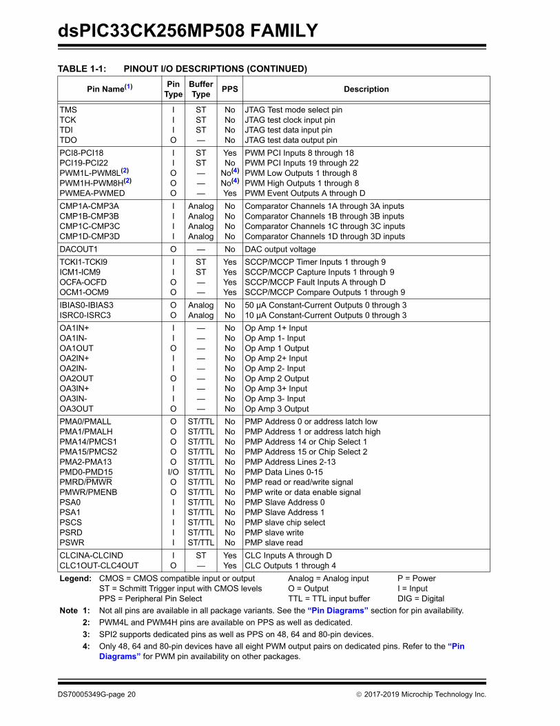
TABLE 1-1: PINOUT I/O DESCRIPTIONS
Pin Name(1) PinType
BufferType PPS Description
AN0-AN23ANA0-ANA1ANN0-ANN2
III
AnalogAnalogAnalog
NoNoNo
Analog input channelsAnalog alternate inputsAnalog negative inputs
ADTRG31 I ST Yes ADC Trigger Input 31CLKI
CLKO
I
O
ST/CMOS
—
No
No
External Clock (EC) source input. Always associated with OSCI pin function.Oscillator crystal output. Connects to crystal or resonator in Crystal Oscillator mode. Optionally functions as CLKO in RC and EC modes. Always associated with OSCO pin function.
OSCI
OSCO
I
I/O
ST/CMOS
—
No
No
Oscillator crystal input. ST buffer when configured in RC mode; CMOS otherwise.Oscillator crystal output. Connects to crystal or resonator in Crystal Oscillator mode. Optionally functions as CLKO in RC and EC modes.
REFCLKOREFOI
OI
—ST
YesYes
Reference clock outputReference clock input
INT0INT1INT2INT3
IIII
STSTSTST
NoYesYesYes
External Interrupt 0External Interrupt 1External Interrupt 2External Interrupt 3
IOCA[4:0]IOCB[15:0]IOCC[15:0]IOCD[15:0]IOCE[15:0]
IIIII
STSTSTSTST
NoNoNoNoNo
Interrupt-on-Change input for PORTAInterrupt-on-Change input for PORTBInterrupt-on-Change input for PORTCInterrupt-on-Change input for PORTDInterrupt-on-Change input for PORTE
RP32-RP71 I/O ST Yes Remappable I/O portsRA0-RA4 I/O ST No PORTA is a bidirectional I/O portRB0-RB15 I/O ST No PORTB is a bidirectional I/O portRC0-RC15 I/O ST No PORTC is a bidirectional I/O portRD0-RD15 I/O ST No PORTD is a bidirectional I/O portRE0-RE15 I/O ST No PORTE is a bidirectional I/O portT1CK I ST Yes Timer1 external clock inputCAN1RXCAN1TX
IO
ST—
YesYes
CAN1 receive inputCAN1 transmit output
U1CTSU1RTSU1RXU1TXU1DSRU1DTR
IOIOIO
ST—ST—ST—
YesYesYesYesYesYes
UART1 Clear-to-SendUART1 Request-to-SendUART1 receiveUART1 transmitUART1 Data-Set-ReadyUART1 Data-Terminal-Ready
Legend: CMOS = CMOS compatible input or output Analog = Analog input P = PowerST = Schmitt Trigger input with CMOS levels O = Output I = Input PPS = Peripheral Pin Select TTL = TTL input buffer DIG = Digital
Note 1: Not all pins are available in all package variants. See the “Pin Diagrams” section for pin availability.2: PWM4L and PWM4H pins are available on PPS as well as dedicated.3: SPI2 supports dedicated pins as well as PPS on 48, 64 and 80-pin devices.4: Only 48, 64 and 80-pin devices have all eight PWM output pairs on dedicated pins. Refer to the “Pin
Diagrams” for PWM pin availability on other packages.
DS70005349G-page 18 2017-2019 Microchip Technology Inc.

dsPIC33CK256MP508 FAMILY
U2CTSU2RTSU2RXU2TXU2DSRU2DTR
IOIOIO
ST—ST—ST—
YesYesYesYesYesYes
UART2 Clear-to-SendUART2 Request-to-SendUART2 receiveUART2 transmitUART2 Data-Set-ReadyUART2 Data-Terminal-Ready
U3CTSU3RTSU3RXU3TXU3DSRU3DTR
IOIOIO
ST—ST—ST—
YesYesYesYesYesYes
UART3 Clear-to-SendUART3 Request-to-SendUART3 receiveUART3 transmitUART3 Data-Set-ReadyUART3 Data-Terminal-Ready
SCK1SDI1SDO1SS1
I/OIO
I/O
STST—ST
YesYesYesYes
Synchronous serial clock input/output for SPI1SPI1 data inSPI1 data outSPI1 slave synchronization or frame pulse I/O
SCK2SDI2SDO2SS2
I/OIO
I/O
STST—ST
Yes(3)
Yes(3)
Yes(3)
Yes(3)
Synchronous serial clock input/output for SPI2SPI2 data inSPI2 data outSPI2 slave synchronization or frame pulse I/O
SCK3SDI3SDO3SS3
I/OIO
I/O
STST—ST
YesYesYesYes
Synchronous serial clock input/output for SPI3SPI3 data inSPI3 data outSPI3 slave synchronization or frame pulse I/O
SCL1SDA1ASCL1ASDA1
I/OI/OI/OI/O
STSTSTST
NoNoNoNo
Synchronous serial clock input/output for I2C1Synchronous serial data input/output for I2C1Alternate synchronous serial clock input/output for I2C1Alternate synchronous serial data input/output for I2C1
SCL2SDA2ASCL2ASDA2
I/OI/OI/OI/O
STSTSTST
NoNoNoNo
Synchronous serial clock input/output for I2C2Synchronous serial data input/output for I2C2Alternate synchronous serial clock input/output for I2C2Alternate synchronous serial data input/output for I2C2
SCL3SDA3ASCL3ASDA3
I/OI/OI/OI/O
STSTSTST
NoNoNoNo
Synchronous serial clock input/output for I2C3Synchronous serial data input/output for I2C3Alternate synchronous serial clock input/output for I2C3Alternate synchronous serial data input/output for I2C3
QEIA1-QEIA2QEIB1-QEIB2QEINDX1-QEINDX2QEIHOM1-QEIHOM2QEICMP1-QEICMP2
IIIIO
STSTSTST—
YesYesYesYesYes
QEI Inputs A1 and A2QEI Inputs B1 and B2QEI Index Inputs 1 and 2QEI Home Inputs 1 and 2QEI Comparator Outputs 1 and 2
SENT1-SENT2SENT1OUT-SENT2OUT
IO
ST—
YesYes
SENT1 and SENT2 inputsSENT1 and SENT2 outputs
TABLE 1-1: PINOUT I/O DESCRIPTIONS (CONTINUED)
Pin Name(1) PinType
BufferType PPS Description
Legend: CMOS = CMOS compatible input or output Analog = Analog input P = PowerST = Schmitt Trigger input with CMOS levels O = Output I = Input PPS = Peripheral Pin Select TTL = TTL input buffer DIG = Digital
Note 1: Not all pins are available in all package variants. See the “Pin Diagrams” section for pin availability.2: PWM4L and PWM4H pins are available on PPS as well as dedicated.3: SPI2 supports dedicated pins as well as PPS on 48, 64 and 80-pin devices.4: Only 48, 64 and 80-pin devices have all eight PWM output pairs on dedicated pins. Refer to the “Pin
Diagrams” for PWM pin availability on other packages.
2017-2019 Microchip Technology Inc. DS70005349G-page 19
dsPIC33CK256MP508 FAMILY
TMSTCKTDITDO
IIIO
STSTST—
NoNoNoNo
JTAG Test mode select pinJTAG test clock input pinJTAG test data input pinJTAG test data output pin
PCI8-PCI18PCI19-PCI22PWM1L-PWM8L(2)
PWM1H-PWM8H(2)
PWMEA-PWMED
IIOOO
STST———
YesNo
No(4)
No(4)
Yes
PWM PCI Inputs 8 through 18PWM PCI Inputs 19 through 22PWM Low Outputs 1 through 8PWM High Outputs 1 through 8PWM Event Outputs A through D
CMP1A-CMP3ACMP1B-CMP3BCMP1C-CMP3CCMP1D-CMP3D
IIII
AnalogAnalogAnalogAnalog
NoNoNoNo
Comparator Channels 1A through 3A inputsComparator Channels 1B through 3B inputsComparator Channels 1C through 3C inputsComparator Channels 1D through 3D inputs
DACOUT1 O — No DAC output voltageTCKI1-TCKI9ICM1-ICM9OCFA-OCFDOCM1-OCM9
IIOO
STST——
YesYesYesYes
SCCP/MCCP Timer Inputs 1 through 9SCCP/MCCP Capture Inputs 1 through 9SCCP/MCCP Fault Inputs A through DSCCP/MCCP Compare Outputs 1 through 9
IBIAS0-IBIAS3ISRC0-ISRC3
OO
AnalogAnalog
NoNo
50 µA Constant-Current Outputs 0 through 310 µA Constant-Current Outputs 0 through 3
OA1IN+OA1IN-OA1OUTOA2IN+OA2IN-OA2OUTOA3IN+OA3IN-OA3OUT
IIOIIOIIO
—————————
NoNoNoNoNoNoNoNoNo
Op Amp 1+ InputOp Amp 1- InputOp Amp 1 OutputOp Amp 2+ InputOp Amp 2- InputOp Amp 2 OutputOp Amp 3+ InputOp Amp 3- InputOp Amp 3 Output
PMA0/PMALLPMA1/PMALHPMA14/PMCS1PMA15/PMCS2PMA2-PMA13PMD0-PMD15PMRD/PMWRPMWR/PMENBPSA0PSA1PSCSPSRDPSWR
OOOOO
I/OOOIIIII
ST/TTLST/TTLST/TTLST/TTLST/TTLST/TTLST/TTLST/TTLST/TTLST/TTLST/TTLST/TTLST/TTL
NoNoNoNoNoNoNoNoNoNoNoNoNo
PMP Address 0 or address latch lowPMP Address 1 or address latch highPMP Address 14 or Chip Select 1PMP Address 15 or Chip Select 2PMP Address Lines 2-13PMP Data Lines 0-15PMP read or read/write signalPMP write or data enable signalPMP Slave Address 0PMP Slave Address 1PMP slave chip selectPMP slave writePMP slave read
CLCINA-CLCINDCLC1OUT-CLC4OUT
IO
ST—
YesYes
CLC Inputs A through DCLC Outputs 1 through 4
TABLE 1-1: PINOUT I/O DESCRIPTIONS (CONTINUED)
Pin Name(1) PinType
BufferType PPS Description
Legend: CMOS = CMOS compatible input or output Analog = Analog input P = PowerST = Schmitt Trigger input with CMOS levels O = Output I = Input PPS = Peripheral Pin Select TTL = TTL input buffer DIG = Digital
Note 1: Not all pins are available in all package variants. See the “Pin Diagrams” section for pin availability.2: PWM4L and PWM4H pins are available on PPS as well as dedicated.3: SPI2 supports dedicated pins as well as PPS on 48, 64 and 80-pin devices.4: Only 48, 64 and 80-pin devices have all eight PWM output pairs on dedicated pins. Refer to the “Pin
Diagrams” for PWM pin availability on other packages.
DS70005349G-page 20 2017-2019 Microchip Technology Inc.

dsPIC33CK256MP508 FAMILY
PGD1PGC1
PGD2PGC2
PGD3PGC3
I/OI
I/OI
I/OI
STST
STST
STST
NoNo
NoNo
NoNo
Data I/O pin for Programming/Debugging Communication Channel 1Clock input pin for Programming/Debugging Communication Channel 1Data I/O pin for Programming/Debugging Communication Channel 2Clock input pin for Programming/Debugging Communication Channel 2Data I/O pin for Programming/Debugging Communication Channel 3Clock input pin for Programming/Debugging Communication Channel 3
MCLR I/P ST No Master Clear (Reset) input. This pin is an active-low Reset to the device.
AVDD P P No Positive supply for analog modules. This pin must be connected at all times.
AVSS P P No Ground reference for analog modules. This pin must be connected at all times.
VDD P — No Positive supply for peripheral logic and I/O pinsVSS P — No Ground reference for logic and I/O pins
TABLE 1-1: PINOUT I/O DESCRIPTIONS (CONTINUED)
Pin Name(1) PinType
BufferType PPS Description
Legend: CMOS = CMOS compatible input or output Analog = Analog input P = PowerST = Schmitt Trigger input with CMOS levels O = Output I = Input PPS = Peripheral Pin Select TTL = TTL input buffer DIG = Digital
Note 1: Not all pins are available in all package variants. See the “Pin Diagrams” section for pin availability.2: PWM4L and PWM4H pins are available on PPS as well as dedicated.3: SPI2 supports dedicated pins as well as PPS on 48, 64 and 80-pin devices.4: Only 48, 64 and 80-pin devices have all eight PWM output pairs on dedicated pins. Refer to the “Pin
Diagrams” for PWM pin availability on other packages.
2017-2019 Microchip Technology Inc. DS70005349G-page 21

dsPIC33CK256MP508 FAMILY
NOTES:
DS70005349G-page 22 2017-2019 Microchip Technology Inc.

dsPIC33CK256MP508 FAMILY
2.0 GUIDELINES FOR GETTING STARTED WITH 16-BIT DIGITAL SIGNAL CONTROLLERS
2.1 Basic Connection RequirementsGetting started with the family devices of thedsPIC33CK256MP508 requires attention to a minimalset of device pin connections before proceeding withdevelopment. The following is a list of pin names whichmust always be connected:• All VDD and VSS pins
(see Section 2.2 “Decoupling Capacitors”)• All AVDD and AVSS pins
regardless if ADC module is not used (see Section 2.2 “Decoupling Capacitors”)
• MCLR pin (see Section 2.3 “Master Clear (MCLR) Pin”)
• PGCx/PGDx pinsused for In-Circuit Serial Programming™ (ICSP™) and debugging purposes (see Section 2.4 “ICSP Pins”)
• OSCI and OSCO pins when an external oscillator source is used (see Section 2.5 “External Oscillator Pins”)
2.2 Decoupling CapacitorsThe use of decoupling capacitors on every pair ofpower supply pins, such as VDD, VSS, AVDD andAVSS is required. Consider the following criteria when using decouplingcapacitors:• Value and type of capacitor: Recommendation
of 0.1 µF (100 nF), 10-20V. This capacitor should be a low-ESR and have resonance frequency in the range of 20 MHz and higher. It is recommended to use ceramic capacitors.
• Placement on the printed circuit board: The decoupling capacitors should be placed as close to the pins as possible. It is recommended to place the capacitors on the same side of the board as the device. If space is constricted, the capacitor can be placed on another layer on the PCB using a via; however, ensure that the trace length from the pin to the capacitor is within one-quarter inch (6 mm) in length.
• Handling high-frequency noise: If the board is experiencing high-frequency noise, above tens of MHz, add a second ceramic-type capacitor in parallel to the above described decoupling capacitor. The value of the second capacitor can be in the range of 0.01 µF to 0.001 µF. Place this second capacitor next to the primary decoupling capacitor. In high-speed circuit designs, consider implementing a decade pair of capacitances as close to the power and ground pins as possible. For example, 0.1 µF in parallel with 0.001 µF.
• Maximizing performance: On the board layout from the power supply circuit, run the power and return traces to the decoupling capacitors first, and then to the device pins. This ensures that the decoupling capacitors are first in the power chain. Equally important is to keep the trace length between the capacitor and the power pins to a minimum, thereby reducing PCB track inductance.
2017-2019 Microchip Technology Inc. DS70005349G-page 23

dsPIC33CK256MP508 FAMILY
FIGURE 2-1: RECOMMENDED MINIMUM CONNECTION
2.2.1 BULK CAPACITORSOn boards with power traces running longer than sixinches in length, it is suggested to use a bulk capacitorfor integrated circuits, including DSCs, to supply a localpower source. The value of the bulk capacitor shouldbe determined based on the trace resistance thatconnects the power supply source to the device andthe maximum current drawn by the device in theapplication. In other words, select the bulk capacitor sothat it meets the acceptable voltage sag at the device.Typical values range from 4.7 µF to 47 µF.
2.3 Master Clear (MCLR) PinThe MCLR pin provides two specific devicefunctions: • Device Reset• Device Programming and Debugging. During device programming and debugging, theresistance and capacitance that can be added to thepin must be considered. Device programmers anddebuggers drive the MCLR pin. Consequently,specific voltage levels (VIH and VIL) and fast signaltransitions must not be adversely affected. Therefore,specific values of R and C will need to be adjustedbased on the application and PCB requirements.For example, as shown in Figure 2-2, it isrecommended that the capacitor, C, be isolated fromthe MCLR pin during programming and debuggingoperations.Place the components, as shown in Figure 2-2,within one-quarter inch (6 mm) from the MCLR pin.
FIGURE 2-2: EXAMPLE OF MCLR PIN CONNECTIONS
Note 1: As an option, instead of a hard-wired connection, an inductor (L1) can be substituted between VDD and AVDD to improve ADC noise rejection. The inductor impedance should be less than 1 and the inductor capacity greater than 10 mA.
Where:
f FCNV2--------------=
f 12 LC
-----------------------=
L 12f C
---------------------- 2
=
(i.e., ADC Conversion Rate/2)
dsPIC33VD
D
VSS
VDD
VSS
VSS
VDD
AVD
D
AVSS
VDD
VSS
0.1 µFCeramic
0.1 µFCeramic
0.1 µFCeramic
0.1 µFCeramic
C
R
VDD
MCLR
0.1 µFCeramic
L1(1)
R1
C
R1(2)R(1)
VDD
MCLR
dsPIC33JP
Note 1: R 10 k is recommended. A suggested starting value is 10 k. Ensure that the MCLR pin VIH and VIL specifications are met.
2: R1 470 will limit any current flowing into MCLR from the external capacitor, C, in the event of MCLR pin breakdown due to Electrostatic Discharge (ESD) or Electrical Overstress (EOS). Ensure that the MCLR pin VIH and VIL specifications are met.
DS70005349G-page 24 2017-2019 Microchip Technology Inc.

dsPIC33CK256MP508 FAMILY
2.4 ICSP PinsThe PGCx and PGDx pins are used for ICSP anddebugging purposes. It is recommended to keep thetrace length between the ICSP connector and the ICSPpins on the device as short as possible. If the ICSP con-nector is expected to experience an ESD event, aseries resistor is recommended, with the value in therange of a few tens of Ohms, not to exceed 100 Ohms. Pull-up resistors, series diodes and capacitors on thePGCx and PGDx pins are not recommended as theywill interfere with the programmer/debugger communi-cations to the device. If such discrete components arean application requirement, they should be removedfrom the circuit during programming and debugging.Alternatively, refer to the AC/DC characteristics andtiming requirements information in the respectivedevice Flash programming specification for informationon capacitive loading limits and pin Voltage Input High(VIH) and Voltage Input Low (VIL) requirements.Ensure that the “Communication Channel Select” (i.e.,PGCx/PGDx pins) programmed into the devicematches the physical connections for the ICSP to theprogrammer/debugger.For more information regarding Microchip’s programmersand debuggers, refer to Section 32.0 “DevelopmentSupport”.
2.5 External Oscillator PinsMany DSCs have options for at least two oscillators: ahigh-frequency Primary Oscillator (POSC) and alow-frequency Secondary Oscillator (SOSC). For details,see Section 9.4 “Primary Oscillator (POSC)”. The oscillator circuit should be placed on the sameside of the board as the device. Also, place the oscil-lator circuit close to the respective oscillator pins, notexceeding one-half inch (12 mm) distance betweenthem. The load capacitors should be placed next tothe oscillator itself, on the same side of the board.Use a grounded copper pour around the oscillatorcircuit to isolate them from surrounding circuits. Thegrounded copper pour should be routed directly to theMCU ground. Do not run any signal traces or powertraces inside the ground pour. Also, if using atwo-sided board, avoid any traces on the other side ofthe board where the crystal is placed. A suggestedlayout is shown in Figure 2-3.
FIGURE 2-3: SUGGESTED PLACEMENT OF THE OSCILLATOR CIRCUIT
Main Oscillator
Guard Ring
Guard Trace
Oscillator Pins
2017-2019 Microchip Technology Inc. DS70005349G-page 25

dsPIC33CK256MP508 FAMILY
2.6 Oscillator Value Conditions on Device Start-up
If the PLL of the target device is enabled andconfigured for the device start-up oscillator, themaximum oscillator source frequency must be limitedto a certain frequency (see Section 9.0 “Oscillatorwith High-Frequency PLL”) to comply with devicePLL start-up conditions. This means that if the externaloscillator frequency is outside this range, the applica-tion must start up in the FRC mode first. The defaultPLL settings after a POR with an oscillator frequencyoutside this range will violate the device operatingspeed.Once the device powers up, the application firmwarecan initialize the PLL SFRs, CLKDIV and PLLFBD, to asuitable value, and then perform a clock switch to theOscillator + PLL clock source. Note that clock switchingmust be enabled in the device Configuration Word.
2.7 Unused I/OsUnused I/O pins should be configured as outputs anddriven to a logic low state.Alternatively, connect a 1k to 10k resistor between VSSand unused pins, and drive the output to logic low.
2.8 Targeted Applications• Power Factor Correction (PFC):
- Interleaved PFC- Critical Conduction PFC- Bridgeless PFC
• DC/DC Converters:- Buck, Boost, Forward, Flyback, Push-Pull- Half/Full-Bridge- Phase-Shift Full-Bridge- Resonant Converters
• DC/AC:- Half/Full-Bridge Inverter- Resonant Inverter
• Motor Control- BLDC- PMSM- SR- ACIM
Examples of typical application connections are shownin Figure 2-4 through Figure 2-6.
FIGURE 2-4: INTERLEAVED PFC
VAC
VOUT+
ADC Channel PWM ADCPWM
|VAC|
k4 k3
FET
dsPIC33CK256MP508
Driver
VOUT-
ADC Channel
ADCChannel Channel
ADCChannel
k2
FETDriver
k1
DS70005349G-page 26 2017-2019 Microchip Technology Inc.

dsPIC33CK256MP508 FAMILY
FIGURE 2-5: PHASE-SHIFTED FULL-BRIDGE CONVERTER
VIN+
VIN-
S1
Gate 4Gate 2
Gate 3Gate 1
AnalogGround
VOUT+
VOUT-
k2FET
Driver
k1
FETDriver
FETDriver
Gate 1
Gate 2
S1 Gate 3
Gate 4
S3
S3
Gate 6
Gate 5
Gat
e 6Gate 5
dsPIC33CK256MP508
PWM
PWM ADCChannel
PWM ADCChannel
2017-2019 Microchip Technology Inc. DS70005349G-page 27

dsPIC33CK256MP508 FAMILY
FIGURE 2-6: OFF-LINE UPS
ADC
ADC
ADC
ADC
ADC
PWM PWMPWM
dsPIC33CK256MP508
PWM PWM PWM
FETDriver k2 k1
FETDriver
FETDriver
FETDriver
FETDriver k4 k5
VBAT
GND
+VOUT+
VOUT-
Full-Bridge InverterPush-Pull ConverterVDC
GND
FETDriver
ADC PWM
k3
k6
orAnalog Comp.
Battery Charger
+
FETDriver
DS70005349G-page 28 2017-2019 Microchip Technology Inc.

dsPIC33CK256MP508 FAMILY
3.0 CPU
The dsPIC33CK256MP508 family CPU has a 16-bit(data) modified Harvard architecture with an enhancedinstruction set, including significant support for DigitalSignal Processing (DSP). The CPU has a 24-bit instruc-tion word with a variable length opcode field. TheProgram Counter (PC) is 23 bits wide and addresses upto 4M x 24 bits of user program memory space. An instruction prefetch mechanism helps maintainthroughput and provides predictable execution. Mostinstructions execute in a single-cycle effective execu-tion rate, with the exception of instructions that changethe program flow, the double-word move (MOV.D)instruction, PSV accesses and the table instructions.Overhead-free program loop constructs are supportedusing the DO and REPEAT instructions, both of whichare interruptible at any point.
3.1 RegistersThe dsPIC33CK256MP508 devices have sixteen, 16-bitWorking registers in the programmer’s model. Each ofthe Working registers can act as a Data, Address orAddress Offset register. The 16th Working register(W15) operates as a Software Stack Pointer forinterrupts and calls.In addition, the dsPIC33CK256MP508 devices includefour Alternate Working register sets, which consist of W0through W14. The Alternate Working registers can bemade persistent to help reduce the saving and restoringof register content during Interrupt Service Routines(ISRs). The Alternate Working registers can be assignedto a specific Interrupt Priority Level (IPL1 through IPL6) byconfiguring the CTXTx[2:0] bits in the FALTREG Configu-ration register. The Alternate Working registers can alsobe accessed manually by using the CTXTSWP instruction.The CCTXI[2:0] and MCTXI[2:0] bits in the CTXTSTATregister can be used to identify the current, and mostrecent, manually selected Working register sets.
3.2 Instruction SetThe instruction set for dsPIC33CK256MP508 deviceshas two classes of instructions: the MCU class ofinstructions and the DSP class of instructions. Thesetwo instruction classes are seamlessly integrated into thearchitecture and execute from a single execution unit.The instruction set includes many addressing modes andwas designed for optimum C compiler efficiency.
3.3 Data Space AddressingThe base Data Space can be addressed as up to4K words or 8 Kbytes, and is split into two blocks,referred to as X and Y data memory. Each memory blockhas its own independent Address Generation Unit(AGU). The MCU class of instructions operates solelythrough the X memory AGU, which accesses the entirememory map as one linear Data Space. Certain DSPinstructions operate through the X and Y AGUs to sup-port dual operand reads, which splits the data addressspace into two parts. The X and Y Data Space boundaryis device-specific.The upper 32 Kbytes of the Data Space memory mapcan optionally be mapped into Program Space (PS) atany 16K program word boundary. The program-to-DataSpace mapping feature, known as Program SpaceVisibility (PSV), lets any instruction access ProgramSpace as if it were Data Space. Refer to “DataMemory” (DS70595) in the “dsPIC33/PIC24 FamilyReference Manual” for more details on PSV and tableaccesses.On dsPIC33CK256MP508 family devices, overhead-free circular buffers (Modulo Addressing) aresupported in both X and Y address spaces. TheModulo Addressing removes the software boundarychecking overhead for DSP algorithms. The X AGUCircular Addressing can be used with any of the MCUclass of instructions. The X AGU also supports Bit-Reversed Addressing to greatly simplify input or outputdata re-ordering for radix-2 FFT algorithms.
3.4 Addressing ModesThe CPU supports these addressing modes:• Inherent (no operand)• Relative• Literal• Memory Direct• Register Direct• Register IndirectEach instruction is associated with a predefinedaddressing mode group, depending upon its functionalrequirements. As many as six addressing modes aresupported for each instruction.
Note 1: This data sheet summarizes the featuresof the dsPIC33CK256MP508 family ofdevices. It is not intended to be a compre-hensive reference source. To complementthe information in this data sheet, refer to“Enhanced CPU” (www.microchip.com/DS70005158) in the “dsPIC33/PIC24Family Reference Manual”.
2: Some registers and associated bitsdescribed in this section may not beavailable on all devices. Refer toSection 4.0 “Memory Organization” inthis data sheet for device-specific registerand bit information.
2017-2019 Microchip Technology Inc. DS70005349G-page 29

dsPIC33CK256MP508 FAMILY
FIGURE 3-1: dsPIC33CK256MP508 FAMILY CPU BLOCK DIAGRAM
InstructionDecode and
Control
16PCL
16
Program Counter
16-Bit ALU
24
24
24
24
X Data Bus
PCU16
16 16
DivideSupport
EngineDSP
RO
M L
atch
16
Y Data Bus
EA MUX
X RAGUX WAGU
Y AGU
16
24
16
16
16
16
16
16
16
8
InterruptController
PSV and TableData AccessControl Block
StackControlLogic
LoopControlLogic
Data LatchData Latch
Y DataRAM
X DataRAM
AddressLatch
AddressLatch
16
Data Latch
16
16
16
X Address Bus
Y Ad
dres
s Bu
s
24
Lite
ral D
ata
Program Memory
Address Latch
Power, Resetand Oscillator
Control Signalsto Various Blocks
Ports
PeripheralModules
Modules
PCH
IR
16-BitWorking Register Arrays
DS70005349G-page 30 2017-2019 Microchip Technology Inc.

dsPIC33CK256MP508 FAMILY
3.4.1 PROGRAMMER’S MODELThe programmer’s model for the dsPIC33CK256MP508family is shown in Figure 3-2. All registers in theprogrammer’s model are memory-mapped and can bemanipulated directly by instructions. Table 3-1 lists adescription of each register.
In addition to the registers contained in the programmer’smodel, the dsPIC33CK256MP508 devices containcontrol registers for Modulo Addressing, Bit-ReversedAddressing and interrupts. These registers are describedin subsequent sections of this document.All registers associated with the programmer’s modelare memory-mapped, as shown in Figure 3-2.
TABLE 3-1: PROGRAMMER’S MODEL REGISTER DESCRIPTIONSRegister(s) Name Description
W0 through W15(1) Working Register ArrayW0 through W14(1) Alternate Working Register Array 1W0 through W14(1) Alternate Working Register Array 2W0 through W14(1) Alternate Working Register Array 3W0 through W14(1) Alternate Working Register Array 4ACCA, ACCB 40-Bit DSP Accumulators (Additional 4 Alternate Accumulators)PC 23-Bit Program CounterSR ALU and DSP Engine STATUS RegisterSPLIM Stack Pointer Limit Value RegisterTBLPAG Table Memory Page Address RegisterDSRPAG Extended Data Space (EDS) Read Page RegisterRCOUNT REPEAT Loop Counter RegisterDCOUNT DO Loop Counter RegisterDOSTARTH, DOSTARTL(2) DO Loop Start Address Register (High and Low)DOENDH, DOENDL DO Loop End Address Register (High and Low)CORCON Contains DSP Engine, DO Loop Control and Trap Status bitsNote 1: Memory-mapped W0 through W14 represent the value of the register in the currently active CPU context.
2: The DOSTARTH and DOSTARTL registers are read-only.
2017-2019 Microchip Technology Inc. DS70005349G-page 31

dsPIC33CK256MP508 FAMILY
FIGURE 3-2: PROGRAMMER’S MODEL
N OV Z C
TBLPAG
PC23 PC0
7 0
D0D15
Program Counter
Data Table Page Address
STATUS Register
Working/AddressRegisters
DSP OperandRegisters
W0 (WREG)W1W2W3
W4W5W6W7W8W9
W10W11W12W13
Frame Pointer/W14Stack Pointer/W15
DSP AddressRegisters
AD39 AD0AD31
DSPAccumulators(1)
ACCA
ACCB
DSRPAG9 0
RA
0
OA OB SA SB
RCOUNT15 0
REPEAT Loop Counter
DCOUNT15 0
DO Loop Counter and Stack
DOSTART23 0
DO Loop Start Address and Stack
0
DOEND DO Loop End Address and Stack
IPL2 IPL1
SPLIM Stack Pointer Limit
AD15
23 0
SRLIPL0
PUSH.S and POP.S Shadows
Nested DO Stack
0
0
OAB SAB
X Data Space Read Page Address
DA DC
0
0
0
0
CORCON15 0
CPU Core Control Register
W0-W3
D15 D0
W0W1W2W3W4
W13W14
W12W11W10W9
W5W6W7W8
W0W1W2W3W4
W13W14
W12
W9
W5W6W7W8
W10W11
D0
AlternateWorking/AddressRegisters
D15
D15D15
D0
D0
W0 W0W1 W1W2 W2W3 W3W4 W4W5 W5W6 W6W7 W7W8 W8W9 W9W10 W10W11 W11W12 W12W13 W13W14 W14
AD39 AD31 AD15 AD0AD39 AD31 AD15 AD0
AD39 AD31 AD15 AD0AD39 AD31 AD15 AD0
DS70005349G-page 32 2017-2019 Microchip Technology Inc.
dsPIC33CK256MP508 FAMILY
3.4.2 CPU RESOURCESMany useful resources are provided on the main prod-uct page of the Microchip website for the devices listedin this data sheet. This product page contains the latestupdates and additional information.
3.4.2.1 Key Resources• “Enhanced CPU” (DS70005158) in the
“dsPIC33/PIC24 Family Reference Manual”• Code Samples• Application Notes• Software Libraries• Webinars• All related “dsPIC33/PIC24 Family Reference
Manual” Sections• Development Tools
2017-2019 Microchip Technology Inc. DS70005349G-page 33

dsPIC33CK256MP508 FAMILY
3.4.3 CPU CONTROL REGISTERS
REGISTER 3-1: SR: CPU STATUS REGISTER
R/W-0 R/W-0 R/W-0 R/W-0 R/C-0 R/C-0 R-0 R/W-0OA OB SA(3) SB(3) OAB SAB DA DC
bit 15 bit 8
R/W-0(2) R/W-0(2) R/W-0(2) R-0 R/W-0 R/W-0 R/W-0 R/W-0IPL2(1) IPL1(1) IPL0(1) RA N OV Z C
bit 7 bit 0
Legend: C = Clearable bitR = Readable bit W = Writable bit U = Unimplemented bit, read as ‘0’-n = Value at POR ‘1’= Bit is set ‘0’ = Bit is cleared x = Bit is unknown
bit 15 OA: Accumulator A Overflow Status bit1 = Accumulator A has overflowed0 = Accumulator A has not overflowed
bit 14 OB: Accumulator B Overflow Status bit1 = Accumulator B has overflowed0 = Accumulator B has not overflowed
bit 13 SA: Accumulator A Saturation ‘Sticky’ Status bit(3)
1 = Accumulator A is saturated or has been saturated at some time0 = Accumulator A is not saturated
bit 12 SB: Accumulator B Saturation ‘Sticky’ Status bit(3)
1 = Accumulator B is saturated or has been saturated at some time0 = Accumulator B is not saturated
bit 11 OAB: OA || OB Combined Accumulator Overflow Status bit1 = Accumulator A or B has overflowed0 = Neither Accumulator A or B has overflowed
bit 10 SAB: SA || SB Combined Accumulator ‘Sticky’ Status bit1 = Accumulator A or B is saturated or has been saturated at some time0 = Neither Accumulator A or B is saturated
bit 9 DA: DO Loop Active bit1 = DO loop is in progress0 = DO loop is not in progress
bit 8 DC: MCU ALU Half Carry/Borrow bit1 = A carry-out from the 4th low-order bit (for byte-sized data) or 8th low-order bit (for word-sized data)
of the result occurred0 = No carry-out from the 4th low-order bit (for byte-sized data) or 8th low-order bit (for word-sized
data) of the result occurred
Note 1: The IPL[2:0] bits are concatenated with the IPL[3] bit (CORCON[3]) to form the CPU Interrupt Priority Level. The value in parentheses indicates the IPL, if IPL[3] = 1. User interrupts are disabled when IPL[3] = 1.
2: The IPL[2:0] Status bits are read-only when the NSTDIS bit (INTCON1[15]) = 1.3: A data write to the SR register can modify the SA and SB bits by either a data write to SA and SB or by
clearing the SAB bit. To avoid a possible SA or SB bit write race condition, the SA and SB bits should not be modified using bit operations.
DS70005349G-page 34 2017-2019 Microchip Technology Inc.

dsPIC33CK256MP508 FAMILY
bit 7-5 IPL[2:0]: CPU Interrupt Priority Level Status bits(1,2)
111 = CPU Interrupt Priority Level is 7 (15); user interrupts are disabled110 = CPU Interrupt Priority Level is 6 (14)101 = CPU Interrupt Priority Level is 5 (13)100 = CPU Interrupt Priority Level is 4 (12)011 = CPU Interrupt Priority Level is 3 (11)010 = CPU Interrupt Priority Level is 2 (10)001 = CPU Interrupt Priority Level is 1 (9)000 = CPU Interrupt Priority Level is 0 (8)
bit 4 RA: REPEAT Loop Active bit1 = REPEAT loop is in progress0 = REPEAT loop is not in progress
bit 3 N: MCU ALU Negative bit1 = Result was negative0 = Result was non-negative (zero or positive)
bit 2 OV: MCU ALU Overflow bitThis bit is used for signed arithmetic (two’s complement). It indicates an overflow of the magnitude thatcauses the sign bit to change state. 1 = Overflow occurred for signed arithmetic (in this arithmetic operation)0 = No overflow occurred
bit 1 Z: MCU ALU Zero bit1 = An operation that affects the Z bit has set it at some time in the past0 = The most recent operation that affects the Z bit has cleared it (i.e., a non-zero result)
bit 0 C: MCU ALU Carry/Borrow bit1 = A carry-out from the Most Significant bit of the result occurred0 = No carry-out from the Most Significant bit of the result occurred
REGISTER 3-1: SR: CPU STATUS REGISTER (CONTINUED)
Note 1: The IPL[2:0] bits are concatenated with the IPL[3] bit (CORCON[3]) to form the CPU Interrupt Priority Level. The value in parentheses indicates the IPL, if IPL[3] = 1. User interrupts are disabled when IPL[3] = 1.
2: The IPL[2:0] Status bits are read-only when the NSTDIS bit (INTCON1[15]) = 1.3: A data write to the SR register can modify the SA and SB bits by either a data write to SA and SB or by
clearing the SAB bit. To avoid a possible SA or SB bit write race condition, the SA and SB bits should not be modified using bit operations.
2017-2019 Microchip Technology Inc. DS70005349G-page 35

dsPIC33CK256MP508 FAMILY
REGISTER 3-2: CORCON: CORE CONTROL REGISTER
R/W-0 U-0 R/W-0 R/W-0 R/W-0 R-0 R-0 R-0VAR — US1 US0 EDT(1) DL2 DL1 DL0
bit 15 bit 8
R/W-0 R/W-0 R/W-1 R/W-0 R/C-0 R-0 R/W-0 R/W-0SATA SATB SATDW ACCSAT IPL3(2) SFA RND IF
bit 7 bit 0
Legend: C = Clearable bitR = Readable bit W = Writable bit U = Unimplemented bit, read as ‘0’-n = Value at POR ‘1’ = Bit is set ‘0’ = Bit is cleared x = Bit is unknown
bit 15 VAR: Variable Exception Processing Latency Control bit1 = Variable exception processing latency is enabled0 = Fixed exception processing latency is enabled
bit 14 Unimplemented: Read as ‘0’bit 13-12 US[1:0]: DSP Multiply Unsigned/Signed Control bits
11 = Reserved10 = DSP engine multiplies are mixed sign01 = DSP engine multiplies are unsigned 00 = DSP engine multiplies are signed
bit 11 EDT: Early DO Loop Termination Control bit(1)
1 = Terminates executing DO loop at the end of the current loop iteration0 = No effect
bit 10-8 DL[2:0]: DO Loop Nesting Level Status bits111 = Seven DO loops are active...001 = One DO loop is active000 = Zero DO loops are active
bit 7 SATA: ACCA Saturation Enable bit1 = Accumulator A saturation is enabled0 = Accumulator A saturation is disabled
bit 6 SATB: ACCB Saturation Enable bit1 = Accumulator B saturation is enabled0 = Accumulator B saturation is disabled
bit 5 SATDW: Data Space Write from DSP Engine Saturation Enable bit1 = Data Space write saturation is enabled0 = Data Space write saturation is disabled
bit 4 ACCSAT: Accumulator Saturation Mode Select bit1 = 9.31 saturation (super saturation)0 = 1.31 saturation (normal saturation)
bit 3 IPL3: CPU Interrupt Priority Level Status bit 3(2)
1 = CPU Interrupt Priority Level is greater than 70 = CPU Interrupt Priority Level is 7 or less
Note 1: This bit is always read as ‘0’.2: The IPL3 bit is concatenated with the IPL[2:0] bits (SR[7:5]) to form the CPU Interrupt Priority Level.
DS70005349G-page 36 2017-2019 Microchip Technology Inc.

dsPIC33CK256MP508 FAMILY
bit 2 SFA: Stack Frame Active Status bit1 = Stack frame is active; W14 and W15 address 0x0000 to 0xFFFF, regardless of DSRPAG0 = Stack frame is not active; W14 and W15 address the base Data Space
bit 1 RND: Rounding Mode Select bit1 = Biased (conventional) rounding is enabled0 = Unbiased (convergent) rounding is enabled
bit 0 IF: Integer or Fractional Multiplier Mode Select bit1 = Integer mode is enabled for DSP multiply0 = Fractional mode is enabled for DSP multiply
REGISTER 3-2: CORCON: CORE CONTROL REGISTER (CONTINUED)
Note 1: This bit is always read as ‘0’.2: The IPL3 bit is concatenated with the IPL[2:0] bits (SR[7:5]) to form the CPU Interrupt Priority Level.
REGISTER 3-3: MSTRPR: EDS BUS MASTER PRIORITY CONTROL REGISTER
U-0 U-0 U-0 U-0 U-0 U-0 U-0 U-0— — — — — — — —
bit 15 bit 8
U-0 U-0 R/W-0 R/W-0 U-0 U-0 U-0 R/W-0— — DMAPR CANPR — — — NVMPR
bit 7 bit 0
Legend:R = Readable bit W = Writable bit U = Unimplemented bit, read as ‘0’-n = Value at POR ‘1’ = Bit is set ‘0’ = Bit is cleared x = Bit is unknown
bit 15-6 Unimplemented: Read as ‘0’bit 5 DMAPR: Modify DMA Controller Bus Master Priority Relative to CPU bit
1 = Raises DMA Controller bus Master priority to above that of the CPU0 = No change to DMA Controller bus Master priority
bit 4 CANPR: Modify CAN1 Bus Master Priority Relative to CPU bit1 = Raises CAN1 bus Master priority to above that of the CPU0 = No change to CAN1 bus Master priority
bit 3-1 Unimplemented: Read as ‘0’bit 0 NVMPR: Modify NVM Controller Bus Master Priority Relative to CPU bit
1 = Raises NVM Controller bus Master priority to above that of the CPU0 = No change to NVM Controller bus Master priority
2017-2019 Microchip Technology Inc. DS70005349G-page 37

dsPIC33CK256MP508 FAMILY
REGISTER 3-4: CTXTSTAT: CPU W REGISTER CONTEXT STATUS REGISTER
U-0 U-0 U-0 U-0 U-0 R-0 R-0 R-0— — — — — CCTXI2 CCTXI1 CCTXI0
bit 15 bit 8
U-0 U-0 U-0 U-0 U-0 R-0 R-0 R-0— — — — — MCTXI2 MCTXI1 MCTXI0
bit 7 bit 0
Legend:R = Readable bit W = Writable bit U = Unimplemented bit, read as ‘0’-n = Value at POR ‘1’ = Bit is set ‘0’ = Bit is cleared x = Bit is unknown
bit 15-11 Unimplemented: Read as ‘0’bit 10-8 CCTXI[2:0]: Current (W Register) Context Identifier bits
111 = Reserved•••100 = Alternate Working Register Set 4 is currently in use011 = Alternate Working Register Set 3 is currently in use010 = Alternate Working Register Set 2 is currently in use 001 = Alternate Working Register Set 1 is currently in use 000 = Default register set is currently in use
bit 7-3 Unimplemented: Read as ‘0’bit 2-0 MCTXI[2:0]: Manual (W Register) Context Identifier bits
111 = Reserved•••100 = Alternate Working Register Set 4 was most recently manually selected011 = Alternate Working Register Set 3 was most recently manually selected010 = Alternate Working Register Set 2 was most recently manually selected001 = Alternate Working Register Set 1 was most recently manually selected000 = Default register set was most recently manually selected
DS70005349G-page 38 2017-2019 Microchip Technology Inc.

dsPIC33CK256MP508 FAMILY
3.4.4 ARITHMETIC LOGIC UNIT (ALU)The dsPIC33CK256MP508 family ALU is 16 bits wideand is capable of addition, subtraction, bit shifts and logicoperations. Unless otherwise mentioned, arithmeticoperations are two’s complement in nature. Dependingon the operation, the ALU can affect the values of theCarry (C), Zero (Z), Negative (N), Overflow (OV) andDigit Carry (DC) Status bits in the SR register. The Cand DC Status bits operate as Borrow and Digit Borrowbits, respectively, for subtraction operations. The ALU can perform 8-bit or 16-bit operations,depending on the mode of the instruction that is used.Data for the ALU operation can come from the Wregister array or data memory, depending on theaddressing mode of the instruction. Likewise, outputdata from the ALU can be written to the W register arrayor a data memory location.Refer to the “16-Bit MCU and DSC Programmer’sReference Manual” (DS70000157) for information onthe SR bits affected by each instruction.The core CPU incorporates hardware support for bothmultiplication and division. This includes a dedicatedhardware multiplier and support hardware for 16-bitdivisor division.
3.4.4.1 MultiplierUsing the high-speed, 17-bit x 17-bit multiplier, the ALUsupports unsigned, signed or mixed-sign operation inseveral MCU multiplication modes:• 16-bit x 16-bit signed• 16-bit x 16-bit unsigned• 16-bit signed x 5-bit (literal) unsigned• 16-bit signed x 16-bit unsigned• 16-bit unsigned x 5-bit (literal) unsigned• 16-bit unsigned x 16-bit signed• 8-bit unsigned x 8-bit unsigned
3.4.4.2 DividerThe divide block supports 32-bit/16-bit and 16-bit/16-bitsigned and unsigned integer divide operations with thefollowing data sizes:• 32-bit signed/16-bit signed divide• 32-bit unsigned/16-bit unsigned divide• 16-bit signed/16-bit signed divide• 16-bit unsigned/16-bit unsigned divideThe 16-bit signed and unsigned DIV instructions canspecify any W register for both the 16-bit divisor (Wn)and any W register (aligned) pair (W(m + 1):Wm) forthe 32-bit dividend. The divide algorithm takes onecycle per bit of divisor, so both 32-bit/16-bit and 16-bit/16-bit instructions take the same number of cycles toexecute. There are additional instructions: DIV2 andDIVF2. Divide instructions will complete in six cycles.
3.4.5 DSP ENGINEThe DSP engine consists of a high-speed 17-bit x 17-bitmultiplier, a 40-bit barrel shifter and a 40-bit adder/subtracter (with two target accumulators, round andsaturation logic).The DSP engine can also perform inherent accumulator-to-accumulator operations that require no additionaldata. These instructions are, ADD, SUB, NEG, MIN andMAX.The DSP engine has options selected through bits inthe CPU Core Control register (CORCON), as listedbelow:• Fractional or integer DSP multiply (IF)• Signed, unsigned or mixed-sign DSP multiply
(USx)• Conventional or convergent rounding (RND)• Automatic saturation on/off for ACCA (SATA)• Automatic saturation on/off for ACCB (SATB)• Automatic saturation on/off for writes to data
memory (SATDW)• Accumulator Saturation mode selection
(ACCSAT)
TABLE 3-2: DSP INSTRUCTIONS SUMMARY
Instruction Algebraic Operation
ACC Write-Back
CLR A = 0 YesED A = (x – y)2 NoEDAC A = A + (x – y)2 NoMAC A = A + (x • y) YesMAC A = A + x2 NoMOVSAC No change in A YesMPY A = x • y NoMPY A = x2 NoMPY.N A = – x • y NoMSC A = A – x • y Yes
2017-2019 Microchip Technology Inc. DS70005349G-page 39

dsPIC33CK256MP508 FAMILY
NOTES:
DS70005349G-page 40 2017-2019 Microchip Technology Inc.

dsPIC33CK256MP508 FAMILY
4.0 MEMORY ORGANIZATION
The dsPIC33CK256MP508 family architecture featuresseparate program and data memory spaces, andbuses. This architecture also allows the direct accessof program memory from the Data Space (DS) duringcode execution.
4.1 Program Address SpaceThe program address memory space of thedsPIC33CK256MP508 family devices is 4M instructions.The space is addressable by a 24-bit value derived eitherfrom the 23-bit PC during program execution, or fromtable operation or Data Space remapping, as describedin Section 4.4.5 “Interfacing Program and DataMemory Spaces”. User application access to the program memory spaceis restricted to the lower half of the address range(0x000000 to 0x7FFFFF). The exception is the use ofTBLRD operations, which use TBLPAG[7] to permitaccess to calibration data and Device ID sections of theconfiguration memory space. The program memory maps for dsPIC33CK256MP508devices are shown in Figure 4-1 through Figure 4-5.
FIGURE 4-1: PROGRAM MEMORY MAP FOR dsPIC33CKXXXMP50X/20X DEVICES(1)
Note: This data sheet summarizes the featuresof the dsPIC33CK256MP508 family ofdevices. It is not intended to be a compre-hensive reference source. To complementthe information in this data sheet, referto “dsPIC33/PIC24 Program Memory”(www.microchip.com/DS70000613) in the“dsPIC33/PIC24 Family ReferenceManual”.
0x000000
Code Memory
0x800000
DEVID
0xFEFFFE0xFF0000
0xFFFFFE
Unimplemented(Read ‘0’s)
Reserved
0x7FFFFE
Con
figur
atio
n M
emor
y Sp
ace
Use
r Mem
ory
Spac
e
Device Configuration
0x0XXX000x0XXXFE
Reserved0xFF0002
Note 1: Memory areas are not shown to scale.2: Calibration data area must be maintained during programming.3: Calibration data area includes UDID, ICSP™ Write Inhibit and FBOOT registers locations.
0xFF0004
Executive Code Memory
0x8018000x8017FE
OTP Memory
0xF9FFFE0xFA00000xFA00020xFA0004
Write Latches
Reserved
0x801700
0x800FFE0x801000
0x8016FE
0x0XXXFE0x0XXX00 See Figure 4-2 through
Figure 4-5 for details.
CalibrationData(2,3)
2017-2019 Microchip Technology Inc. DS70005349G-page 41

dsPIC33CK256MP508 FAMILY
FIGURE 4-2: PROGRAM MEMORY MAP FOR dsPIC33CK256MP50/20X DEVICES(1)
FIGURE 4-3: PROGRAM MEMORY MAP FOR dsPIC33CK128MP50X/20X DEVICES(1)
0x000000
User
0x02BF000x02BEFE
Program
Unimplemented(Read ‘0’s)
Inac
tive
Parti
tion
Activ
e Pa
rtitio
n
Device Configuration
0x02C0000x02BFFE
0x7FFFFE
Note 1: Memory areas are not shown to scale.
Single Partition Dual Partition
Memory
0x000000User
0x0160000x015FFE
Program
Unimplemented(Read ‘0’s)
Inac
tive
Parti
tion
Activ
e Pa
rtitio
n
Device Configuration
0x400000
0x7FFFFE
Memory
UserProgramMemory
Unimplemented(Read ‘0’s)
Device Configuration
0x015EFE0x015F00
0x415F000x415EFE
0x4160000x415FFE
0x000000
User
0x015F000x015EFE
Program
Unimplemented(Read ‘0’s)
Inac
tive
Parti
tion
Activ
e Pa
rtitio
n
Device Configuration
0x0160000x015FFE
0x7FFFFE
Note 1: Memory areas are not shown to scale.
Single Partition Dual Partition
Memory
0x000000User
0x00B0000x00AFFE
Program
Unimplemented(Read ‘0’s)
Inac
tive
Parti
tion
Activ
e Pa
rtitio
n
Device Configuration
0x400000
0x7FFFFE
Memory
UserProgramMemory
Unimplemented(Read ‘0’s)
Device Configuration
0x00AEFE0x00AF00
0x40AF000x40AEFE
0x40B0000x40AFFE
DS70005349G-page 42 2017-2019 Microchip Technology Inc.

dsPIC33CK256MP508 FAMILY
FIGURE 4-4: PROGRAM MEMORY MAP FOR dsPIC33CK64MP50X/20X DEVICES(1)
FIGURE 4-5: PROGRAM MEMORY MAP FOR dsPIC33CK32MP50X/20X DEVICES(1)
0x000000
User
0x00AF000x00AEFE
Program
Unimplemented(Read ‘0’s)
Inac
tive
Parti
tion
Activ
e Pa
rtitio
n
Device Configuration
0x00B0000x00AFFE
0x7FFFFE
Note 1: Memory areas are not shown to scale.
Single Partition Dual Partition
Memory
0x000000User
0x0058000x0057FE
Program
Unimplemented(Read ‘0’s)
Inac
tive
Parti
tion
Activ
e Pa
rtitio
n
Device Configuration
0x400000
0x7FFFFE
Memory
UserProgramMemory
Unimplemented(Read ‘0’s)
Device Configuration
0x0056FE0x005700
0x4057000x4056FE
0x4058000x4057FE
0x000000
User
0x005F000x005EFE
Program
Unimplemented(Read ‘0’s)
Inac
tive
Parti
tion
Activ
e Pa
rtitio
n
Device Configuration
0x0060000x005FFE
0x7FFFFE
Note 1: Memory areas are not shown to scale.
Single Partition Dual Partition
Memory
0x000000User
0x0030000x002FFE
Program
Unimplemented(Read ‘0’s)
Inac
tive
Parti
tion
Activ
e Pa
rtitio
n
Device Configuration
0x400000
0x7FFFFE
Memory
UserProgramMemory
Unimplemented(Read ‘0’s)
Device Configuration
0x002EFE0x002F00
0x402F000x402EFE
0x4030000x402FFE
2017-2019 Microchip Technology Inc. DS70005349G-page 43

dsPIC33CK256MP508 FAMILY
4.1.1 PROGRAM MEMORY ORGANIZATION
The program memory space is organized in word-addressable blocks. Although it is treated as 24 bitswide, it is more appropriate to think of each address ofthe program memory as a lower and upper word, withthe upper byte of the upper word being unimplemented.The lower word always has an even address, while theupper word has an odd address (Figure 4-6). Program memory addresses are always word-alignedon the lower word, and addresses are incremented ordecremented, by two, during code execution. Thisarrangement provides compatibility with data memoryspace addressing and makes data in the programmemory space accessible.
4.1.2 INTERRUPT AND TRAP VECTORSAll dsPIC33CK256MP508 family devices reserve theaddresses between 0x000000 and 0x000200 for hard-coded program execution vectors. A hardware Resetvector is provided to redirect code execution from thedefault value of the PC on device Reset to the actualstart of code. A GOTO instruction is programmed by theuser application at address, 0x000000, of Flashmemory, with the actual address for the start of code ataddress, 0x000002, of Flash memory.A more detailed discussion of the Interrupt VectorTables (IVTs) is provided in Section 7.0 “InterruptController”.
FIGURE 4-6: PROGRAM MEMORY ORGANIZATION
0816
PC Address
0x0000000x0000020x0000040x000006
230000000000000000
0000000000000000
Program Memory‘Phantom’ Byte
(read as ‘0’)
least significant wordmost significant word
Instruction Width
0x0000010x0000030x0000050x000007
mswAddress (lsw Address)
DS70005349G-page 44 2017-2019 Microchip Technology Inc.

dsPIC33CK256MP508 FAMILY
4.1.3 UNIQUE DEVICE IDENTIFIER (UDID)
All dsPIC33CK256MP508 family devices are individu-ally encoded during final manufacturing with a UniqueDevice Identifier or UDID. The UDID cannot be erasedby a bulk erase command or any other user-accessiblemeans. This feature allows for manufacturing trace-ability of Microchip Technology devices in applicationswhere this is a requirement. It may also be used by theapplication manufacturer for any number of things thatmay require unique identification, such as:• Tracking the device• Unique serial number• Unique security keyThe UDID comprises five 24-bit program words. Whentaken together, these fields form a unique 120-bitidentifier.The UDID is stored in five read-only locations, locatedbetween 0x801200 and 0x801208 in the device config-uration space. Table 4-1 lists the addresses of theIdentifier Words and shows their contents.
4.2 Data Address SpaceThe dsPIC33CK256MP508 family CPU has a separate16-bit wide data memory space. The Data Space isaccessed using separate Address Generation Units(AGUs) for read and write operations. The datamemory maps are shown in Figure 4-7, Figure 4-8 andFigure 4-9.All Effective Addresses (EAs) in the data memory spaceare 16 bits wide and point to bytes within the DataSpace. This arrangement gives a base Data Spaceaddress range of 64 Kbytes or 32K words.The lower half of the data memory space (i.e., whenEA[15] = 0) is used for implemented memoryaddresses, while the upper half (EA[15] = 1) isreserved for the Program Space Visibility (PSV).The dsPIC33CK256MP508 family devices implementup to 16 Kbytes of data memory. If an EA points to alocation outside of this area, an all-zero word or byte isreturned.
4.2.1 DATA SPACE WIDTHThe data memory space is organized in byte-addressable, 16-bit wide blocks. Data are aligned indata memory and registers as 16-bit words, but all DataSpace EAs resolve to bytes. The Least SignificantBytes (LSBs) of each word have even addresses, whilethe Most Significant Bytes (MSBs) have oddaddresses.
4.2.2 DATA MEMORY ORGANIZATION AND ALIGNMENT
To maintain backward compatibility with PIC® MCUdevices and improve Data Space memory usageefficiency, the dsPIC33CK256MP508 family instructionset supports both word and byte operations. As aconsequence of byte accessibility, all Effective Addresscalculations are internally scaled to step through word-aligned memory. For example, the core recognizes thatPost-Modified Register Indirect Addressing mode[Ws++] results in a value of Ws + 1 for byte operationsand Ws + 2 for word operations. A data byte read, reads the complete word thatcontains the byte, using the LSb of any EA to determinewhich byte to select. The selected byte is placed ontothe LSB of the data path. That is, data memory andregisters are organized as two parallel, byte-wideentities with shared (word) address decode, butseparate write lines. Data byte writes only write to thecorresponding side of the array or register that matchesthe byte address. All word accesses must be aligned to an even address.Misaligned word data fetches are not supported, socare must be taken when mixing byte and wordoperations, or translating from 8-bit MCU code. If amisaligned read or write is attempted, an address errortrap is generated. If the error occurred on a read, theinstruction underway is completed. If the error occurredon a write, the instruction is executed but the write doesnot occur. In either case, a trap is then executed,allowing the system and/or user application to examinethe machine state prior to execution of the addressFault.All byte loads into any W register are loaded into theLSB; the MSB is not modified.A Sign-Extend (SE) instruction is provided to allow userapplications to translate 8-bit signed data to 16-bitsigned values. Alternatively, for 16-bit unsigned data,user applications can clear the MSB of any W registerby executing a Zero-Extend (ZE) instruction on theappropriate address.
TABLE 4-1: UDID ADDRESSESUDID Address Description
UDID1 0x801200 UDID Word 1UDID2 0x801202 UDID Word 2UDID3 0x801204 UDID Word 3UDID4 0x801206 UDID Word 4UDID5 0x801208 UDID Word 5
2017-2019 Microchip Technology Inc. DS70005349G-page 45

dsPIC33CK256MP508 FAMILY
4.2.3 SFR SPACEThe first four Kbytes of the Near Data Space, from0x0000 to 0x0FFF, is primarily occupied by SpecialFunction Registers (SFRs). These are used by thedsPIC33CK256MP508 family core and peripheralmodules for controlling the operation of the device. SFRs are distributed among the modules that theycontrol and are generally grouped together by module.Much of the SFR space contains unused addresses;these are read as ‘0’.
4.2.4 NEAR DATA SPACE The 8-Kbyte area, between 0x0000 and 0x1FFF, isreferred to as the Near Data Space. Locations in thisspace are directly addressable through a 13-bit absoluteaddress field within all memory direct instructions. Addi-tionally, the whole Data Space is addressable using MOVinstructions, which support Memory Direct Addressingmode with a 16-bit address field, or by using IndirectAddressing mode using a Working register as anAddress Pointer.
Note: The actual set of peripheral features andinterrupts varies by the device. Refer to thecorresponding device tables and pinoutdiagrams for device-specific information.
DS70005349G-page 46 2017-2019 Microchip Technology Inc.

dsPIC33CK256MP508 FAMILY
FIGURE 4-7: DATA MEMORY MAP FOR dsPIC33CK256MPX0X DEVICES
0x0000
0x0FFE
0xFFFE
LSBAddress16 Bits
LSBMSB
MSBAddress
0x0001
0x0FFF
0xFFFF
OptionallyMappedinto ProgramMemory
0x1001
4-KbyteSFR Space
24-KbyteSRAM Space
Data SpaceNear8-Kbyte
SFR Space
X Data RAM (X) (8K)
X DataUnimplemented (X)
0x80000x8001
Note: Memory areas are not shown to scale.
Y Data RAM (Y) (8K)
0x4FFF 0x4FFE0x5001 0x5000
0x6FFF 0x6FFE0x7001 0x7000
0x2000
2017-2019 Microchip Technology Inc. DS70005349G-page 47

dsPIC33CK256MP508 FAMILY
FIGURE 4-8: DATA MEMORY MAP FOR dsPIC33CK128MPX0X DEVICES
0x0000
0x0FFE
0xFFFE
LSBAddress16 Bits
LSBMSB
MSBAddress
0x0001
0x0FFF
0xFFFF
OptionallyMappedinto ProgramMemory
0x1001
4-KbyteSFR Space
16-KbyteSRAM Space
Data SpaceNear8-Kbyte
SFR Space
X Data RAM (X) (8K)
X DataUnimplemented (X)
0x80000x8001
Note: Memory areas are not shown to scale.
Y Data RAM (Y) (8K)
0x2FFF 0x2FFE0x3001 0x3000
0x4FFF 0x4FFE0x5001 0x5000
0x2000
DS70005349G-page 48 2017-2019 Microchip Technology Inc.

dsPIC33CK256MP508 FAMILY
FIGURE 4-9: DATA MEMORY MAP FOR dsPIC33CK64MPX0X AND dsPIC33CK32MPX0X DEVICES
0x0000
0x0FFE
0xFFFE
LSBAddress16 Bits
LSBMSB
MSBAddress
0x0001
0x0FFF
0xFFFF
OptionallyMappedinto ProgramMemory
0x1001
4-KbyteSFR Space
8-KbyteSRAM Space
Data SpaceNear8-Kbyte
SFR Space
X Data RAM (X) (8K)
X DataUnimplemented (X)
0x80000x8001
Note: Memory areas are not shown to scale.
Y Data RAM (Y) (8K)
0x1FFF 0x1FFE0x2001 0x2000
0x2FFF 0x2FFE0x3001 0x3000
0x2000
2017-2019 Microchip Technology Inc. DS70005349G-page 49

dsPIC33CK256MP508 FAMILY
4.2.5 X AND Y DATA SPACESThe dsPIC33CK256MP508 family core has two DataSpaces, X and Y. These Data Spaces can be consideredeither separate (for some DSP instructions) or as oneunified linear address range (for MCU instructions). TheData Spaces are accessed using two Address Genera-tion Units (AGUs) and separate data paths. This featureallows certain instructions to concurrently fetch twowords from RAM, thereby enabling efficient execution ofDSP algorithms, such as Finite Impulse Response (FIR)filtering and Fast Fourier Transform (FFT).The X Data Space is used by all instructions andsupports all addressing modes. X Data Space hasseparate read and write data buses. The X read databus is the read data path for all instructions that viewData Space as combined X and Y address space. It isalso the X data prefetch path for the dual operand DSPinstructions (MAC class). The Y Data Space is used in concert with the X DataSpace by the MAC class of instructions (CLR, ED,EDAC, MAC, MOVSAC, MPY, MPY.N and MSC) to providetwo concurrent data read paths. Both the X and Y Data Spaces support Modulo Address-ing mode for all instructions, subject to addressing moderestrictions. Bit-Reversed Addressing mode is onlysupported for writes to X Data Space. All data memory writes, including in DSP instructions,view Data Space as combined X and Y address space.The boundary between the X and Y Data Spaces isdevice-dependent and is not user-programmable.
4.2.6 BIST OVERVIEWThe dsPIC33CK256MP508 family features a datamemory Built-In Self-Test (BIST) that has the option tobe run at start-up or run time. The memory test checksthat all memory locations are functional and provides apass/fail status of the RAM that can be used by soft-ware to take action if needed. If a failure is reported, thespecific location(s) are not identified.The MBISTCON register (Register 4-1) contains controland status bits for BIST operation. The MBISTDONE bit(MBISTCON[7]) indicates if a BIST was run since thelast Reset and the MBISTSTAT bit (MBISTCON[4])provides the pass fail result.
4.2.7 BIST AT START-UPThe BIST can be configured to automatically run on aPOR type Reset, as shown in Figure 4-10. By default,when BISTDIS (FPOR[6]) = 1, the BIST is disabled andwill not be part of device start-up. If the BISTDIS bit iscleared during device programming, the BIST will runafter all Configuration registers have been loaded andbefore code execution begins. BIST will always run onFRC+PLL with PLL settings resulting in a 125 MHzclock rate.
FIGURE 4-10: BIST FLOWCHART
4.2.8 BIST AT RUN TIMEA BIST test can be requested to run on subsequentdevice Resets at any time. A BIST will corrupt all of the RAM contents, including theStack Pointer, and requires a subsequent Reset. Thesystem should be prepared for a Reset before a BIST isperformed. The BIST is invoked by setting the MBISTENbit (MBISTCON[0]) and executing a Reset. TheMBISTCON register is protected against accidentalwrites and requires an unlock sequence prior to writing.Only one bit can be set per unlock sequence. Theprocedure for a run-time BIST is as follows:1. Execute the unlock sequence by consecutively
writing 0x55 and 0xAA to the NVMKEY register.2. Write 0x0001 to the MBISTCON SFR.3. Execute a software RESET command.4. Verify a Software Reset has occurred by reading
SWR (RCON[6]) (optional).5. Verify that the MBISTDONE bit is set.6. Take action depending on test result indicated
by MBISTSTAT.
POR
BIST
BISTDIS(FPOR[6])
Code Execution
1
0
DS70005349G-page 50 2017-2019 Microchip Technology Inc.

dsPIC33CK256MP508 FAMILY
4.2.8.1 Fault SimulationA mechanism is available to simulate a BIST failure toallow testing of Fault handling software. When theFLTINJ bit is set during a run-time BIST, theMBISTSTAT bit will be set regardless of the test result.The procedure for a BIST Fault simulation is as follows:
1. Execute the unlock sequence by consecutivelywriting 0x55 and 0xAA to the NVMKEY register.
2. Set the MBISTEN bit (MBISTCON[0]).3. Execute 2nd unlock sequence by consecutively
writing 0x55 and 0xAA to the NVMKEY register.4. Set the FLTINJ bit (MBISTCON[8]).5. Execute a software RESET command.6. Verify the MBISTDONE, MBSITSTAT and FLTINJ
bits are all set.
REGISTER 4-1: MBISTCON: MBIST CONTROL REGISTER
U-0 U-0 U-0 U-0 U-0 U-0 U-0 R/W-0(1)
— — — — — — — FLTINJbit 15 bit 8
R/W/HS-0 U-0 U-0 R-0 U-0 U-0 U-0 R/W/HC-0MBISTDONE(1) — — MBISTSTAT — — — MBISTEN(2)
bit 7 bit 0
Legend: HS = Hardware Settable bit HC = Hardware Clearable bitR = Readable bit W = Writable bit U = Unimplemented bit, read as ‘0’-n = Value at POR ‘1’ = Bit is set ‘0’ = Bit is cleared x = Bit is unknown
bit 15-9 Unimplemented: Read as ‘0’bit 8 FLTINJ: MBIST Fault Inject Control bit(1)
1 = The MBIST test will complete and sets MBISTSTAT = 1, simulating an SRAM test failure0 = The MBIST test will execute normally
bit 7 MBISTDONE: MBIST Done Status bit(1)
1 = An MBIST operation has been executed0 = No MBIST operation has occurred on the last Reset sequence
bit 6-5 Unimplemented: Read as ‘0’bit 4 MBISTSTAT: MBIST Status bit
1 = The last MBIST failed0 = The last MBIST passed; all memory may not have been tested
bit 3-1 Unimplemented: Read as ‘0’bit 0 MBISTEN: MBIST Enable bit(2)
1 = MBIST test is armed; an MBIST test will execute at the next device Reset0 = MBIST test is disarmed
Note 1: HW resets only on a true POR Reset.2: This bit will self-clear when the MBIST test is complete.
2017-2019 Microchip Technology Inc. DS70005349G-page 51

dsPIC33CK256MP508 FAMILY
4.3 Memory ResourcesMany useful resources are provided on the mainproduct page of the Microchip website for the deviceslisted in this data sheet. This product page contains thelatest updates and additional information.
4.3.1 KEY RESOURCES• “Enhanced CPU” (DS70005158) in the
“dsPIC33/PIC24 Family Reference Manual”• Code Samples• Application Notes• Software Libraries
• Webinars• All Related “dsPIC33/PIC24 Family Reference
Manual” Sections• Development Tools
4.4 SFR MapsThe following tables show the dsPIC33CK256MP508family SFR names, addresses and Reset values.These tables contain all registers applicable to thedsPIC33CK256MP508 family. Not all registers arepresent on all device variants. Refer to Table 1 andTable 2 for peripheral availability. Table 8-1 details portavailability for the different package options.
TABLE 4-2: SFR BLOCK 000h Register Address All Resets Register Address All Resets Register Address All Resets
Core XMODSRT 048 xxxxxxxxxxxxxxx0 CRCWREG0 000 0000000000000000 XMODEND 04A xxxxxxxxxxxxxxx1 CRCCONL 0B0 --000000010000--WREG1 002 0000000000000000 YMODSRT 04C xxxxxxxxxxxxxxx0 CRCCONH 0B2 ---00000---00000WREG2 004 0000000000000000 YMODEND 04E xxxxxxxxxxxxxxx1 CRCXORL 0B4 000000000000000-WREG3 006 0000000000000000 XBREV 050 xxxxxxxxxxxxxxxx CRCXORH 0B6 0000000000000000WREG4 008 0000000000000000 DISICNT 052 -xxxxxxxxxxxxx00 CRCDATL 0B8 0000000000000000WREG5 00A 0000000000000000 TBLPAG 054 --------00000000 CRCDATH 0BA 0000000000000000WREG6 00C 0000000000000000 YPAG 056 --------00000001 CRCWDATL 0BC 0000000000000000WREG7 00E 0000000000000000 MSTRPR 058 ----------00---0 CRCWDATH 0BE 0000000000000000WREG8 010 0000000000000000 CTXTSTAT 05A -----000-----000 CLCWREG9 012 0000000000000000 DMTCON 05C ---------------- CLC1CONL 0C0 --0-00--000--000WREG10 014 0000000000000000 DMTPRECLR 060 xxxxxxxx-------- CLC1CONH 0C2 ------------0000WREG11 016 0000000000000000 DMTCLR 064 --------xxxxxxxx CLC1SEL 0C4 0000-000-000-000WREG12 018 0000000000000000 DMTSTAT 068 --------xxx----x CLC1GLSL 0C8 0000000000000000WREG13 01A 0000000000000000 DMTCNTL 06C xxxxxxxxxxxxxxxx CLC1GLSH 0CA 0000000000000000WREG14 01C 0000000000000000 DMTCNTH 06E xxxxxxxxxxxxxxxx CLC2CONL 0CC --0-00--000--000WREG15 01E 0001000000000000 DMTHOLDREG 070 xxxxxxxxxxxxxxxx CLC2CONH 0CE ------------0000
SPLIM 020 xxxxxxxxxxxxxxxx DMTPSCNTL 074 xxxxxxxxxxxxxxxx CLC2SELL 0D0 0000-000-000-000ACCAL 022 xxxxxxxxxxxxxxxx DMTPSCNTH 076 xxxxxxxxxxxxxxxx CLC2GLSL 0D4 0000000000000000ACCAH 024 xxxxxxxxxxxxxxxx DMTPSINTVL 078 xxxxxxxxxxxxxxxx CLC2GLSH 0D6 0000000000000000ACCAU 026 xxxxxxxxxxxxxxxx DMTPSINTVH 07A xxxxxxxxxxxxxxxx CLC3CONL 0D8 --0-00--000--000ACCBL 028 xxxxxxxxxxxxxxxx SENT CLC3CONH 0DA ------------0000ACCBH 02A xxxxxxxxxxxxxxxx SENT1CON1 080 --0-000000-0-000 CLC3SELL 0DC 0000-000-000-000ACCBU 02C xxxxxxxxxxxxxxxx SENT1CON2 084 0000000000000000 CLC3GLSL 0E0 0000000000000000
PCL 02E 0000000000000000 SENT1CON3 088 0000000000000000 CLC3GLSH 0E2 0000000000000000PCH 030 --------00000000 SENT1STAT 08C --------00000000 CLC4CONL 0E4 --0-00--000--000
DSRPAG 032 ------0000000001 SENT1SYNC 090 0000000000000000 CLC4CONH 0E6 ------------0000DSWPAG 034 -------000000001 SENT1DATL 094 0000000000000000 CLC4SELL 0E8 0000-000-000-000RCOUNT 036 xxxxxxxxxxxxxxxx SENT1DATH 096 0000000000000000 CLC4GLSL 0EC 0000000000000000DCOUNT 038 xxxxxxxxxxxxxxxx SENT2CON1 098 --0-000000-0-000 CLC4GLSH 0EE 0000000000000000
DOSTARTL 03A xxxxxxxxxxxxxxx0 SENT2CON2 09C 0000000000000000 ECCDOSTARTH 03C ---------xxxxxxx SENT2CON3 0A0 0000000000000000 ECCCONL 0F0 ---------------0
DOENDL 03E xxxxxxxxxxxxxxx0 SENT2STAT 0A4 --------00000000 ECCCONH 0F2 0000000000000000DOENDH 040 ---------xxxxxxx SENT2SYNC 0A8 0000000000000000 ECCADDRL 0F4 0000000000000000
SR 042 0000000000000000 SENT2DATL 0AC 0000000000000000 ECCADDRH 0F6 0000000000000000CORCON 044 --xx000000100000 SENT2DATH 0AE 0000000000000000 ECCSTATL 0F8 0000000000000000MODCON 046 0--0000000000000 ECCSTATH 0FA ------0000000000
Legend: x = unknown or indeterminate value; “-” = unimplemented bits. Address values are in hexadecimal. Reset values are in binary.
DS70005349G-page 52 2017-2019 Microchip Technology Inc.

dsPIC33CK256MP508 FAMILY
TABLE 4-3: SFR BLOCK 100h Register Address All Resets Register Address All Resets Register Address All Resets
Timers INDX1HLD 16A 0000000000000000 INDX2HLD 19E 0000000000000000T1CON 100 --0000000-00-00- QEI1GECL/
QEI1ICL16C 0000000000000000 QEI2GECL/
QEI2ICL1A0 0000000000000000
TMR1 104 0000000000000000 QEI1GECH/QEI1ICH
16E 0000000000000000 QEI2GECH/QEI2ICH
1A2 0000000000000000
PR1 108 0000000000000000 QEI1LECL 170 0000000000000000 QEI2LECL 1A4 0000000000000000QEI QEI1LECH 172 0000000000000000 QEI2LECH 1A6 0000000000000000
QEI1CON 140 --000000-0000000 QEI2CON 174 --000000-0000000 PMPQEI1IOC 144 000000000000xxxx QEI2IOC 178 000000000000xxxx PMCON 1A8 --00000000000-00
QEI1IOCH 146 ---------------0 QEI2IOCH 17A ---------------0 PMCONH 1AA --------0-----0-QEI1STAT 148 --00000000000000 QEI2STAT 17C --00000000000000 PMMODE 1AC 0000000000000000
POS1CNTL 14C 0000000000000000 POS2CNTL 180 0000000000000000 PMADDR 1B0 0000000000000000POS1CNTH 14E 0000000000000000 POS2CNTH 182 0000000000000000 PMDOUT1 1B4 0000000000000000POS1HLD 152 0000000000000000 POS2HLD 186 0000000000000000 PMDOUT2 1B6 0000000000000000VEL1CNT 154 0000000000000000 VEL2CNT 188 0000000000000000 PMDIN1 1B8 0000000000000000
VEL1CNTH 156 0000000000000000 VEL2CNTH 18A 0000000000000000 PMDIN2 1BA 0000000000000000VEL1HLD 15A 0000000000000000 VEL2HLD 18E 0000000000000000 PMAEN 1BC 0000000000000000INT1TMRL 15C 0000000000000000 INT2TMRL 190 0000000000000000 PMSTAT 1C0 00--000010--1111INT1TMRH 15E 0000000000000000 INT2TMRH 192 0000000000000000 PMWADDR 1C4 0000000000000000INT1HLDL 160 0000000000000000 INT2HLDL 194 0000000000000000 PMRADDR 1C8 0000000000000000INT1HLDH 162 0000000000000000 INT2HLDH 196 0000000000000000 PMRDIN 1CC 0000000000000000
INDX1CNTL 164 0000000000000000 INDX2CNTL 198 0000000000000000INDX1CNTH 166 0000000000000000 INDX2CNTH 19A 0000000000000000Legend: x = unknown or indeterminate value; “-” = unimplemented bits. Address values are in hexadecimal. Reset values are in binary.
2017-2019 Microchip Technology Inc. DS70005349G-page 53

dsPIC33CK256MP508 FAMILY
TABLE 4-4: SFR BLOCK 200h Register Address All Resets Register Address All Resets Register Address All Resets
I2C1 and I2C2 U1SCCON 258 ----------00000- SPI1IMSKH 2C2 --0000000-000000I2C1CONL 200 --01000000000000 U1SCINT 25A --00-000--00-000 SPI1URDTL 2C4 0000000000000000I2C1CONH 202 ---------0000000 U1INT 25C --------00---0-- SPI1URDTH 2C6 0000000000000000I2C1STAT 204 000--00000000000 U2MODE 260 --000-0000000000 SPI2CON1L 2C8 --00000000000000I2C1ADD 208 ------0000000000 U2MODEH 262 00---00000000000 SPI2CON1H 2CA 0000000000000000I2C1MSK 20C ------0000000000 U2STA 264 0000000010000000 SPI2CON2L 2CC -----------00000I2C1BRG 210 0000000000000000 U2STAH 266 0000-00000101110 SPI2CON2H 2CE ----------------I2C1TRN 214 --------11111111 U2BRG 268 0000000000000000 SPI2STATL 2D0 ---00--0001-1-00I2C1RCV 218 --------00000000 U2BRGH 26A ------------0000 SPI2STATH 2D2 --000000--000000
I2C2CONL 21C --01000000000000 U2RXREG 26C --------xxxxxxxx SPI2BUFL 2D4 0000000000000000I2C2CONH 21E ---------0000000 U2TXREG 270 --------xxxxxxxx SPI2BUFH 2D6 0000000000000000I2C2STAT 220 000--00000000000 U2P1 274 -------000000000 SPI2BRGL 2D8 ---xxxxxxxxxxxxxI2C2ADD 224 ------0000000000 U2P2 276 -------000000000 SPI2BRGH 2DA ----------------I2C2MSK 228 ------0000000000 U2P3 278 0000000000000000 SPI2IMSKL 2DC ---00--0000-0-00I2C2BRG 22C 0000000000000000 U2P3H 27A --------00000000 SPI2IMSKH 2DE --0000000-000000I2C2TRN 230 --------11111111 U2TXCHK 27C --------00000000 SPI2URDTL 2E0 0000000000000000I2C2RCV 234 --------00000000 U2RXCHK 27E --------00000000 SPI2URDTH 2E2 0000000000000000
UART1 and UART2 U2SCCON 280 ----------00000- SPI3CON1L 2E4 --00000000000000U1MODE 238 --000-0000000000 U2SCINT 282 --00-000--00-000 SPI3CON1H 2E6 0000000000000000
U1MODEH 23A 00---00000000000 U2INT 284 --------00---0-- SPI3CON2L 2E8 -----------00000U1STA 23C 0000000010000000 SPI SPI3CON2H 2EA ----------------
U1STAH 23E 0000-00000101110 SPI1CON1L 2AC --00000000000000 SPI3STATL 2EC ---00--0001-1-00U1BRG 240 0000000000000000 SPI1CON1H 2AE 0000000000000000 SPI3STATH 2EE --000000--000000
U1BRGH 242 ------------0000 SPI1CON2L 2B0 -----------00000 SPI3BUFL 2F0 0000000000000000U1RXREG 244 --------xxxxxxxx SPI1CON2H 2B2 ---------------- SPI3BUFH 2F2 0000000000000000U1TXREG 248 --------xxxxxxxx SPI1STATL 2B4 ---00--0001-1-00 SPI3BRGL 2F4 ---xxxxxxxxxxxxx
U1P1 24C -------000000000 SPI1STATH 2B6 --000000--000000 SPI3BRGH 2F6 ----------------U1P2 24E -------000000000 SPI1BUFL 2B8 0000000000000000 SPI3IMSKL 2F8 ---00--0000-0-00U1P3 250 0000000000000000 SPI1BUFH 2BA 0000000000000000 SPI3IMSKH 2FA --0000000-000000
U1P3H 252 --------00000000 SPI1BRGL 2BC ---xxxxxxxxxxxxx SPI3URDTL 2FC 0000000000000000U1TXCHK 254 --------00000000 SPI1BRGH 2BE ---------------- SPI3URDTH 2F3 0000000000000000U1RXCHK 256 --------00000000 SPI1IMSKL 2C0 ---00--0000-0-00
Legend: x = unknown or indeterminate value; “-” = unimplemented bits. Address values are in hexadecimal. Reset values are in binary.
DS70005349G-page 54 2017-2019 Microchip Technology Inc.

dsPIC33CK256MP508 FAMILY
TABLE 4-5: SFR BLOCK 300hRegister Address All Resets Register Address All Resets Register Address All Resets
High-Speed PWM PG1TRIGA 354 0000000000000000 PG3CLPCIH 3AA 0000-00000000000PCLKCON 300 00-----0--00--00 PG1TRIGB 356 0000000000000000 PG3FFPCIL 3AC 0000000000000000
FSCL 302 0000000000000000 PG1TRIGC 358 0000000000000000 PG3FFPCIH 3AE 0000-00000000000FSMINPER 304 0000000000000000 PG1DTL 35A --00000000000000 PG3SPCIL 3B0 0000000000000000MPHASE 306 0000000000000000 PG1DTH 35C --00000000000000 PG3SPCIH 3B2 0000-00000000000
MDC 308 0000000000000000 PG1CAP 35E 0000000000000000 PG3LEBL 3B4 0000000000000000MPER 30A 0000000000000000 PG2CONL 360 -----0000--00000 PG3LEBH 3B6 -----000----0000LFSR 30C 0000000000000000 PG2CONH 362 000-000000--0000 PG3PHASE 3B8 0000000000000000
CMBTRIGL 30E --------00000000 PG2STAT 364 0000000000000000 PG3DC 3BA 0000000000000000CMBTRIGH 310 --------00000000 PG2IOCONL 366 0000000000000000 PG3DCA 3BC --------00000000LOGCONA 312 000000000000-000 PG2IOCONH 368 0000---0--000000 PG3PER 3BE 0000000000000000LOGCONB 314 000000000000-000 PG2EVTL 36A 00000000---00000 PG3TRIGA 3C0 0000000000000000LOGCONC 316 000000000000-000 PG2EVTH 36C 0000--0000000000 PG3TRIGB 3C2 0000000000000000LOGCOND 318 000000000000-000 PG2FPCIL 36E 0000000000000000 PG3TRIGC 3C4 0000000000000000LOGCONE 31A 000000000000-000 PG2FPCIH 370 0000-00000000000 PG3DTL 3C6 --00000000000000LOGCONF 31C 000000000000-000 PG2CLPCIL 372 0000000000000000 PG3DTH 3C8 --00000000000000PWMEVTA 31E 0000----0000-000 PG2CLPCIH 374 0000-00000000000 PG3CAP 3CA 0000000000000000PWMEVTB 320 0000----0000-000 PG2FFPCIL 376 0000000000000000 PG4CONL 3CC -----0000--00000PWMEVTC 322 0000----0000-000 PG2FFPCIH 378 0000-00000000000 PG4CONH 3CE 000-000000--0000PWMEVTD 324 0000----0000-000 PG2SPCIL 37A 0000000000000000 PG4STAT 3D0 0000000000000000PWMEVTE 326 0000----0000-000 PG2SPCIH 37C 0000-00000000000 PG4IOCONL 3D2 0000000000000000PWMEVTF 328 0000----0000-000 PG2LEBL 37E 0000000000000000 PG4IOCONH 3D4 0000---0--000000PG1CONL 32A -----0000--00000 PG2LEBH 380 -----000----0000 PG4EVTL 3D6 00000000---00000PG1CONH 32C 000-000000--0000 PG2PHASE 382 0000000000000000 PG4EVTH 3D8 0000--0000000000PG1STAT 32E 0000000000000000 PG2DC 384 0000000000000000 PG4FPCIL 3DA 0000000000000000
PG1IOCONL 330 0000000000000000 PG2DCA 386 --------00000000 PG4FPCIH 3DC 0000-00000000000PG1IOCONH 332 0000---0--000000 PG2PER 388 0000000000000000 PG4CLPCIL 3DE 0000000000000000
PG1EVTL 334 00000000---00000 PG2TRIGA 38A 0000000000000000 PG4CLPCIH 3E0 0000-00000000000PG1EVTH 336 0000--0000000000 PG2TRIGB 38C 0000000000000000 PG4FFPCIL 3E2 0000000000000000PG1FPCIL 338 0000000000000000 PG2TRIGC 38E 0000000000000000 PG4FFPCIH 3E4 0000-00000000000PG1FPCIH 33A 0000-00000000000 PG2DTL 390 --00000000000000 PG4SPCIL 3E6 0000000000000000PG1CLPCIL 33C 0000000000000000 PG2DTH 392 --00000000000000 PG4SPCIH 3E8 0000-00000000000PG1CLPCIH 33E 0000-00000000000 PG2CAP 394 0000000000000000 PG4LEBL 3EA 0000000000000000PG1FFPCIL 340 0000000000000000 PG3CONL 396 -----0000--00000 PG4LEBH 3EC -----000----0000PG1FFPCIH 342 0000-00000000000 PG3CONH 398 000-000000--0000 PG4PHASE 3EE 0000000000000000PG1SPCIL 344 0000000000000000 PG3STAT 39A 0000000000000000 PG4DC 3F0 0000000000000000PG1SPCIH 346 0000-00000000000 PG3IOCONL 39C 0000000000000000 PG4DCA 3F2 --------00000000PG1LEBL 348 0000000000000000 PG3IOCONH 39E 0000---0--000000 PG4PER 3F4 0000000000000000PG1LEBH 34A -----000----0000 PG3EVTL 3A0 00000000---00000 PG4TRIGA 3F6 0000000000000000
PG1PHASE 34C 0000000000000000 PG3EVTH 3A2 0000--0000000000 PG4TRIGB 3F8 0000000000000000PG1DC 34E 0000000000000000 PG3FPCIL 3A4 0000000000000000 PG4TRIGC 3FA 0000000000000000
PG1DCA 350 --------00000000 PG3FPCIH 3A6 0000-00000000000 PG4DTL 3FC --00000000000000PG1PER 352 0000000000000000 PG3CLPCIL 3A8 0000000000000000 PG4DTH 3FE --00000000000000
Legend: x = unknown or indeterminate value; “-” = unimplemented bits. Address values are in hexadecimal. Reset values are in binary.
2017-2019 Microchip Technology Inc. DS70005349G-page 55

dsPIC33CK256MP508 FAMILY
TABLE 4-6: SFR BLOCK 400hRegister Address All Resets Register Address All Resets Register Address All Resets
High-Speed PWM (Continued) PG6FPCIH 448 0000-00000000000 PG7DC 492 0000000000000000PG4CAP 400 0000000000000000 PG6CLPCIL 44A 0000000000000000 PG7DCA 494 --------00000000
PG5CONL 402 -----0000--00000 PG6CLPCIH 44C 0000-00000000000 PG7PER 496 0000000000000000PG5CONH 404 000-000000--0000 PG6FFPCIL 44E 0000000000000000 PG7TRIGA 498 0000000000000000PG5STAT 406 0000000000000000 PG6FFPCIH 450 0000-00000000000 PG7TRIGB 49A 0000000000000000
PG5IOCONL 408 0000000000000000 PG6SPCIL 452 0000000000000000 PG7TRIGC 49C 0000000000000000PG5IOCONH 40A 0000---0--000000 PG6SPCIH 454 0000-00000000000 PG7DTL 49E --00000000000000
PG5EVTL 40C 00000000---00000 PG6LEBL 456 0000000000000000 PG7DTH 4A0 --00000000000000PG5EVTH 40E 0000--0000000000 PG6LEBH 458 -----000----0000 PG7CAP 4A2 0000000000000000PG5FPCIL 410 0000000000000000 PG6PHASE 45A 0000000000000000 PG8CONL 4A4 -----0000--00000PG5FPCIH 412 0000-00000000000 PG6DC 45C 0000000000000000 PG8CONH 4A6 000-000000--0000PG5CLPCIL 414 0000000000000000 PG6DCA 45E --------00000000 PG8STAT 4A8 0000000000000000PG5CLPCIH 416 0000-00000000000 PG6PER 460 0000000000000000 PG8IOCONL 4AA 0000000000000000PG5FFPCIL 418 0000000000000000 PG6TRIGA 462 0000000000000000 PG8IOCONH 4AC 0000---0--000000PG5FFPCIH 41A 0000-00000000000 PG6TRIGB 464 0000000000000000 PG8EVTL 4AE 00000000---00000PG5SPCIL 41C 0000000000000000 PG6TRIGC 466 0000000000000000 PG8EVTH 4B0 0000--0000000000PG5SPCIH 41E 0000-00000000000 PG6DTL 468 --00000000000000 PG8FPCIL 4B2 0000000000000000PG5LEBL 420 0000000000000000 PG6DTH 46A --00000000000000 PG8FPCIH 4B4 0000-00000000000PG5LEBH 422 -----000----0000 PG6CAP 46C 0000000000000000 PG8CLPCIL 4B6 0000000000000000
PG5PHASE 424 0000000000000000 PG7CONL 46E -----0000--00000 PG8CLPCIH 4B8 0000-00000000000PG5DC 426 0000000000000000 PG7CONH 470 000-000000--0000 PG8FFPCIL 4BA 0000000000000000
PG5DCA 428 --------00000000 PG7STAT 472 0000000000000000 PG8FFPCIH 4BC 0000-00000000000PG5PER 42A 0000000000000000 PG7IOCONL 474 0000000000000000 PG8SPCIL 4BE 0000000000000000
PG5TRIGA 42C 0000000000000000 PG7IOCONH 476 0000---0--000000 PG8SPCIH 4C0 0000-00000000000PG5TRIGB 42E 0000000000000000 PG7EVTL 478 00000000---00000 PG8LEBL 4C2 0000000000000000PG5TRIGC 430 0000000000000000 PG7EVTH 47A 0000--0000000000 PG8LEBH 4C4 -----000----0000
PG5DTL 432 --00000000000000 PG7FPCIL 47C 0000000000000000 PG8PHASE 4C6 0000000000000000PG5DTH 434 --00000000000000 PG7FPCIH 47E 0000-00000000000 PG8DC 4C8 0000000000000000PG5CAP 436 0000000000000000 PG7CLPCIL 480 0000000000000000 PG8DCA 4CA --------00000000
PG6CONL 438 -----0000--00000 PG7CLPCIH 482 0000-00000000000 PG8PER 4CC 0000000000000000PG6CONH 43A 000-000000--0000 PG7FFPCIL 484 0000000000000000 PG8TRIGA 4CE 0000000000000000PG6STAT 43C 0000000000000000 PG7FFPCIH 486 0000-00000000000 PG8TRIGB 4D0 0000000000000000
PG6IOCONL 43E 0000000000000000 PG7SPCIL 488 0000000000000000 PG8TRIGC 4D2 0000000000000000PG6IOCONH 440 0000---0--000000 PG7SPCIH 48A 0000-00000000000 PG8DTL 4D4 --00000000000000
PG6EVTL 442 00000000---00000 PG7LEBL 48C 0000000000000000 PG8DTH 4D6 --00000000000000PG6EVTH 444 0000--0000000000 PG7LEBH 48E -----000----0000 PG8CAP 4D8 0000000000000000PG6FPCIL 446 0000000000000000 PG7PHASE 490 0000000000000000
Legend: x = unknown or indeterminate value; “-” = unimplemented bits. Address values are in hexadecimal. Reset values are in binary.
DS70005349G-page 56 2017-2019 Microchip Technology Inc.

dsPIC33CK256MP508 FAMILY
TABLE 4-7: SFR BLOCK 500h Register Address All Resets Register Address All Resets Register Address All Resets
CAN C1TSCONL 5D4 ------0000000000 C1RXOVIFH 5EA 0000000000000000C1CONL 5C0 --00011101100000 C1TSCONH 5D6 -------------000 C1TXATIFL 5EC 0000000000000000C1CONH 5C2 0000010010011000 C1VECL 5D8 ---00000-1000000 C1TXATIFH 5EE 0000000000000000
C1NBTCFGL 5C4 00001111-0001111 C1VECH 5DA 11000000-1000000 C1TXREQL 5F0 0000000000000000C1NBTCFGH 5C6 0000000000111110 C1INTL 5DC 000000-----00000 C1TXREQH 5F2 0000000000000000C1DBTCFGL 5C8 ----0011----0011 C1INTH 5DE 000000-----00000 C1TRECL 5F4 0000000000000000C1DBTCFGH 5CA 00000000---01110 C1RXIFL 5E0 0000000000000000 C1TRECH 5F6 ----------100000
C1TDCL 5CC 00010000--000000 C1RXIFH 5E2 0000000000000000 C1BDIAG0L 5F8 0000000000000000C1TDCH 5CE ------00------10 C1TXIFL 5E4 000000000000000- C1BDIAG0H 5FA 0000000000000000C1TBCL 5D0 0000000000000000 C1TXIFH 5E6 0000000000000000 C1BDIAG1L 5FC 0000000000000000C1TBCH 5D2 0000000000000000 C1RXOVIFL 5E8 000000000000000- C1BDIAG1H 5FE 00000-000-000000
Legend: x = unknown or indeterminate value; “-” = unimplemented bits. Address values are in hexadecimal. Reset values are in binary.
2017-2019 Microchip Technology Inc. DS70005349G-page 57

dsPIC33CK256MP508 FAMILY
TABLE 4-8: SFR BLOCK 600h Register Address All Resets Register Address All Resets Register Address All Resets
CAN (Continued) C1FIFOSTA6 65C ---0000000000000 C1FLTOBJ6L 6B0 0000000000000000C1TEFCONL 600 -----1-0--0-0000 C1FIFOUA6L 660 xxxxxxxxxxxxxxxx C1FLTOBJ6H 6B2 0000000000000000C1TEFCONH 602 ---00000-------- C1FIFOUA6H 662 xxxxxxxxxxxxxxxx C1MASK6L 6B4 0000000000000000C1TEFSTA 604 ------------0000 C1FIFOCON7L 664 -----100x0000000 C1MASK6H 6B6 0000000000000000C1TEFUAL 608 xxxxxxxxxxxxxxxx C1FIFOCON7H 666 00000000-1100000 C1FLTOBJ7L 7B8 0000000000000000C1TEFUAH 60A xxxxxxxxxxxxxxxx C1FIFOSTA7 668 ---0000000000000 C1FLTOBJ7H 6BA 0000000000000000C1FIFOBAL 60C 0000000000000000 C1FIFOUA7L 66C xxxxxxxxxxxxxxxx C1MASK7L 6BC 0000000000000000C1FIFOBAH 60E 0000000000000000 C1FIFOUA7H 66E xxxxxxxxxxxxxxxx C1MASK7H 6BE 0000000000000000C1TXQCONL 610 -----100x0000000 C1FLTCON0L 670 ---000000--00000 C1FLTOBJ8L 6C0 0000000000000000C1TXQCONH 612 00000000-1100000 C1FLTCON0H 672 ---000000--00000 C1FLTOBJ8H 6C2 0000000000000000C1TXQSTA 614 ---000000000-0-0 C1FLTCON1L 674 ---000000--00000 C1MASK8L 6C4 0000000000000000C1TXQUAL 618 xxxxxxxxxxxxxxxx C1FLTCON1H 676 ---000000--00000 C1MASK8H 6C6 0000000000000000C1TXQUAH 61A xxxxxxxxxxxxxxxx C1FLTCON2L 678 ---000000--00000 C1FLTOBJ9L 6C8 0000000000000000
C1FIFOCON1L 61C -----100x0000000 C1FLTCON2H 67A ---000000--00000 C1FLTOBJ9H 6CA 0000000000000000C1FIFOCON1H 61E 00000000-1100000 C1FLTCON3L 67C ---000000--00000 C1MASK9L 6CC 0000000000000000C1FIFOSTA1 620 ---0000000000000 C1FLTCON3H 67E ---000000--00000 C1MASK9H 6CE 0000000000000000C1FIFOUA1L 624 xxxxxxxxxxxxxxxx C1FLTOBJ0L 680 0000000000000000 C1FLTOBJ10L 6D0 0000000000000000C1FIFOUA1H 626 xxxxxxxxxxxxxxxx C1FLTOBJ0H 682 0000000000000000 C1FLTOBJ10H 6D2 0000000000000000
C1FIFOCON2L 628 -----100x0000000 C1MASK0L 684 0000000000000000 C1MASK10L 6D4 0000000000000000C1FIFOCON2H 62A 00000000-1100000 C1MASK0H 686 0000000000000000 C1MASK10H 6D6 0000000000000000C1FIFOSTA2 62C ---0000000000000 C1FLTOBJ1L 688 0000000000000000 C1FLTOBJ11L 6D8 0000000000000000C1FIFOUA2L 630 xxxxxxxxxxxxxxxx C1FLTOBJ1H 68A 0000000000000000 C1FLTOBJ11H 6DA 0000000000000000C1FIFOUA2H 632 xxxxxxxxxxxxxxxx C1MASK1L 68C 0000000000000000 C1MASK11L 6DC 0000000000000000
C1FIFOCON3L 634 -----100x0000000 C1MASK1H 68E 0000000000000000 C1MASK11H 6DE 0000000000000000C1FIFOCON3H 636 00000000-1100000 C1FLTOBJ2L 690 0000000000000000 C1FLTOBJ12L 6E0 0000000000000000C1FIFOSTA3 638 ---0000000000000 C1FLTOBJ2H 692 0000000000000000 C1FLTOBJ12H 6E2 0000000000000000C1FIFOUA3L 63C xxxxxxxxxxxxxxxx C1MASK2L 694 0000000000000000 C1MASK12L 6E4 0000000000000000C1FIFOUA3H 63E xxxxxxxxxxxxxxxx C1MASK2H 696 0000000000000000 C1MASK12H 6E6 0000000000000000
C1FIFOCON4L 640 -----100x0000000 C1FLTOBJ3L 698 0000000000000000 C1FLTOBJ13L 6E8 0000000000000000C1FIFOCON4H 642 00000000-1100000 C1FLTOBJ3H 69A 0000000000000000 C1FLTOBJ13H 6EA 0000000000000000C1FIFOSTA4 644 ---0000000000000 C1MASK3L 69C 0000000000000000 C1MASK13L 6EC 0000000000000000C1FIFOUA4L 648 xxxxxxxxxxxxxxxx C1MASK3H 69C 0000000000000000 C1MASK13H 6EE 0000000000000000C1FIFOUA4H 64A xxxxxxxxxxxxxxxx C1FLTOBJ4L 6A0 0000000000000000 C1FLTOBJ14L 6F0 0000000000000000
C1FIFOCON5L 64C -----100x0000000 C1FLTOBJ4H 6A2 0000000000000000 C1FLTOBJ14H 6F2 0000000000000000C1FIFOCON5H 64E 00000000-1100000 C1MASK4L 6A4 0000000000000000 C1MASK14L 6F4 0000000000000000C1FIFOSTA5 650 ---0000000000000 C1MASK4H 6A6 0000000000000000 C1MASK14H 6F6 0000000000000000C1FIFOUA5L 654 xxxxxxxxxxxxxxxx C1FLTOBJ5L 6A8 0000000000000000 C1FLTOBJ15L 6F8 0000000000000000C1FIFOUA5H 656 xxxxxxxxxxxxxxxx C1FLTOBJ5H 6AA 0000000000000000 C1FLTOBJ15H 6FA 0000000000000000
C1FIFOCON6L 658 -----100x0000000 C1MASK5L 6AC 0000000000000000 C1MASK15L 6FC 0000000000000000C1FIFOCON6H 65A 00000000-1100000 C1MASK5H 6AE 0000000000000000 C1MASK15H 6FE 0000000000000000Legend: x = unknown or indeterminate value; “-” = unimplemented bits. Address values are in hexadecimal. Reset values are in binary.
DS70005349G-page 58 2017-2019 Microchip Technology Inc.

dsPIC33CK256MP508 FAMILY
TABLE 4-9: SFR BLOCK 800h Register Address All Resets Register Address All Resets Register Address All Resets
Interrupts IPC3 846 -100-100-100-100 IPC35 886 -100-100--------IFS0 800 0000000000-00000 IPC4 848 -100-100-100-100 IPC36 888 -------------100IFS1 802 000000000-000000 IPC5 84A -100-----100-100 IPC37 88A -----100-100----IFS2 804 00000-00-0000--- IPC6 84C -100-100-100-100 IPC38 88C ---------100-100IFS3 806 00000000-0-00000 IPC7 84E -100-100-100-100 IPC40 890 ---------100-100IFS4 808 0000000000000-00 IPC8 850 -100-100-------- IPC42 894 -100-100-100-100IFS5 80A 000000000000000- IPC9 852 -----100-100-100 IPC43 896 -100-100-100-100IFS6 80C 0000000000000000 IPC10 854 -100-----100-100 IPC44 898 -100-100-100-100IFS7 80E 0000000000000000 IPC11 856 -100-100-100-100 IPC45 89A -----100-100-100IFS8 810 00-------------0 IPC12 858 -100-100-100-100 IPC47 89E -100-100-100----IFS9 812 ------00-00----0 IPC13 85A -----100-----100 IPC48 8A0 -100-100-100-100IFS10 814 00000000------00 IPC14 85C -100-100-100-100 INTCON1 8C0 0000000000-0000-IFS11 816 000------0000000 IPC15 85E -100-100-100---- INTCON2 8C2 000----0----0000IFS12 818 ------------0000 IPC16 860 -100-----100-100 INTCON3 8C4 ------00---0---0IEC0 820 0000000000-00000 IPC17 862 -100-100-100-100 INTCON4 8C6 --------------00IEC1 822 000000000-000000 IPC18 864 -100-100-100-100 INTTREG 8C8 000-0000-0000000IEC2 824 00000-00-0000--- IPC19 866 -100-100-100-100 FlashIEC3 826 00000000-0-00000 IPC20 868 -100-100-100---- NVMCON 8D0 00000000----0000IEC4 828 0000000000000-00 IPC21 86A -100-100-100-100 NVMADR 8D2 0000000000000000IEC5 82A 000000000000000- IPC22 86C -100-100-100-100 NVMADRU 8D4 --------00000000IEC6 82C 0000000000000000 IPC23 86E -100-100-100-100 NVMKEY 8D6 --------00000000IEC7 82E 0000000000000000 IPC24 870 -100-100-100-100 NVMSRCADRL 8D8 0000000000000000IEC8 830 0--------------0 IPC25 872 -100-100-100-100 NVMSRCADRH 8DA --------00000000IEC9 832 ------00-00----0 IPC26 874 -100-100-100-100 CBG
IEC10 834 00000000------00 IPC27 876 -100-100-100-100 AMPCON1L 8DC -------------000IEC11 836 000------0000000 IPC28 878 -100-100-100-100 AMPCON1H 8DE -------------000IEC12 838 ------------0000 IPC29 87A -100-100-100-100 BIASCON 8F0 ------------0000IPC0 840 -100-100-100-100 IPC30 87C -100-100-100-100 IBIASCON0L 8F4 --000000--000000IPC1 842 -100-100-----100 IPC31 87E -100-100-100-100 IBIASCON0H 8F6 --000000--000000IPC2 844 -100-100-100-100 IPC32 880 -------------100
Legend: x = unknown or indeterminate value; “-” = unimplemented bits. Address values are in hexadecimal. Reset values are in binary.
2017-2019 Microchip Technology Inc. DS70005349G-page 59

dsPIC33CK256MP508 FAMILY
TABLE 4-10: SFR BLOCK 900h Register Address All Resets Register Address All Resets Register Address All Resets
PTG CCP1CON2L 954 00-0----00000000 CCP3TMRH 9AA 0000000000000000PTGCST 900 --00-00000x---00 CCP1CON2H 956 -------100-00000 CCP3PRL 9AC 1111111111111111PTGCON 902 000000000000-000 CCP1CON3H 95A 0000------0-00-- CCP3PRH 9AE 1111111111111111PTGBTE 904 xxxxxxxxxxxxxxxx CCP1STATL 95C -----0--00xx0000 CCP3RAL 9B0 0000000000000000
PTGBTEH 906 0000000000000000 CCP1TMRL 960 0000000000000000 CCP3RBL 9B4 0000000000000000PTGHOLD 908 0000000000000000 CCP1TMRH 962 0000000000000000 CCP3BUFL 9B8 0000000000000000PTGT0LIM 90C 0000000000000000 CCP1PRL 964 1111111111111111 CCP3BUFH 9BA 0000000000000000PTGT1LIM 910 0000000000000000 CCP1PRH 966 1111111111111111 CCP4CON1L 9BC --00000000000000PTGSDLIM 914 0000000000000000 CCP1RAL 968 0000000000000000 CCP4CON1H 9BE 00--000000000000PTGC0LIM 918 0000000000000000 CCP1RBL 96C 0000000000000000 CCP4CON2L 9C0 00-0----00000000PTGC1LIM 91C 0000000000000000 CCP1BUFL 970 0000000000000000 CCP4CON2H 9C2 -------100-00000PTGADJ 920 0000000000000000 CCP1BUFH 972 0000000000000000 CCP4CON3H 9C6 0000------0-00--PTGL0 924 0000000000000000 CCP2CON1L 974 --00000000000000 CCP4STATL 9C8 -----0--00xx0000
PTGQPTR 928 -----------00000 CCP2CON1H 976 00--000000000000 CCP4TMRL 9CC 0000000000000000PTGQUE0 930 xxxxxxxxxxxxxxxx CCP2CON2L 978 00-0----00000000 CCP4TMRH 9CE 0000000000000000PTGQUE1 932 xxxxxxxxxxxxxxxx CCP2CON2H 97A 0------100-00000 CCP4PRL 9D0 1111111111111111PTGQUE2 934 xxxxxxxxxxxxxxxx CCP2CON3H 97E 0000------0-00-- CCP4PRH 9D2 1111111111111111PTGQUE3 936 xxxxxxxxxxxxxxxx CCP2STATL 980 -----0--00xx0000 CCP4RAL 9D4 0000000000000000PTGQUE4 938 xxxxxxxxxxxxxxxx CCP2TMRL 984 0000000000000000 CCP4RBL 9D8 0000000000000000PTGQUE5 93A xxxxxxxxxxxxxxxx CCP2TMRH 986 0000000000000000 CCP4BUFL 9DC 0000000000000000PTGQUE6 93C xxxxxxxxxxxxxxxx CCP2PRL 988 1111111111111111 CCP4BUFH 9DE 0000000000000000PTGQUE7 93E xxxxxxxxxxxxxxxx CCP2PRH 98A 1111111111111111 CCP5CON1L 9E0 --00000000000000PTGQUE8 940 xxxxxxxxxxxxxxxx CCP2RAL 98C 0000000000000000 CCP5CON1H 9E2 00--000000000000PTGQUE9 942 xxxxxxxxxxxxxxxx CCP2RBL 990 0000000000000000 CCP5CON2L 9E4 00-0----00000000PTGQUE10 944 xxxxxxxxxxxxxxxx CCP2BUFL 994 0000000000000000 CCP5CON2H 9E6 -------100-00000PTGQUE11 946 xxxxxxxxxxxxxxxx CCP2BUFH 996 0000000000000000 CCP5CON3H 9EA 0000------0-00--PTGQUE12 948 xxxxxxxxxxxxxxxx CCP3CON1L 998 --00000000000000 CCP5STATL 9EC -----0--00xx0000PTGQUE13 94A xxxxxxxxxxxxxxxx CCP3CON1H 99A 00--000000000000 CCP5TMRL 9F0 0000000000000000PTGQUE14 94C xxxxxxxxxxxxxxxx CCP3CON2L 99C 00-0----00000000 CCP5TMRH 9F2 0000000000000000PTGQUE15 94E xxxxxxxxxxxxxxxx CCP3CON2H 99E -------100-00000 CCP5PRL 9F4 1111111111111111
CCP CCP3CON3H 9A2 0000------0-00-- CCP5PRH 9F6 1111111111111111CCP1CON1L 950 --00000000000000 CCP3STATL 9A4 -----0--00xx0000 CCP5RAL 9F8 0000000000000000CCP1CON1H 952 00--000000000000 CCP3TMRL 9A8 0000000000000000 CCP5RBL 9FC 0000000000000000CCP1CON2L 954 00-0----00000000Legend: x = unknown or indeterminate value; “-” = unimplemented bits. Address values are in hexadecimal. Reset values are in binary.
DS70005349G-page 60 2017-2019 Microchip Technology Inc.

dsPIC33CK256MP508 FAMILY
TABLE 4-11: SFR BLOCK A00h Register Address All Resets Register Address All Resets Register Address All Resets
CCP (Continued) CCP7BUFL A48 0000000000000000 CCP9BUFL A90 0000000000000000CCP5BUFL A00 0000000000000000 CCP7BUFH A4A 0000000000000000 CCP9BUFH A92 0000000000000000CCP5BUFH A02 0000000000000000 CCP8CON1L A4C --00000000000000 DMA
CCP6CON1L A04 --00000000000000 CCP8CON1H A4E 00--000000000000 DMACON ABC --0------------0CCP6CON1H A06 00--000000000000 CCP8CON2L A50 00-0----00000000 DMABUF ABE 0000000000000000CCP6CON2L A08 00-0----00000000 CCP8CON2H A52 0------100-00000 DMAL AC0 0000000000000000CCP6CON2H A0A -------100-00000 CCP8CON3H A56 0000------0-00-- DMAH AC2 0000000000000000CCP6CON3H A0E 0000------0-00-- CCP8STATL A58 -----0--00xx0000 DMACH0 AC4 -----00000000000CCP6STATL A10 -----0--00xx0000 CCP8TMRL A5C 0000000000000000 DMAINT0 AC6 --00000000000--0CCP6TMRL A14 0000000000000000 CCP8TMRH A5E 0000000000000000 DMASRC0 AC8 0000000000000000CCP6TMRH A16 0000000000000000 CCP8PRL A60 1111111111111111 DMADST0 ACA 0000000000000000CCP6PRL A18 1111111111111111 CCP8PRH A62 1111111111111111 DMACNT0 ACC 0000000000000001CCP6PRH A1A 1111111111111111 CCP8RAL A64 0000000000000000 DMACH1 ACE -----00000000000CCP6RAL A1C 0000000000000000 CCP8RBL A68 0000000000000000 DMAINT1 AD0 --00000000000--0CCP6RBL A20 0000000000000000 CCP8BUFL A6C 0000000000000000 DMASRC1 AD2 0000000000000000
CCP6BUFL A24 0000000000000000 CCP8BUFH A6E 0000000000000000 DMADST1 AD4 0000000000000000CCP6BUFH A26 0000000000000000 CCP9CON1L A70 --00000000000000 DMACNT1 AD6 0000000000000001
CCP7CON1L A28 --00000000000000 CCP9CON1H A72 00--000000000000 DMACH2 AD8 -----00000000000CCP7CON1H A2A 00--000000000000 CCP9CON2L A74 00-0----00000000 DMAINT2 ADA --00000000000--0CCP7CON2L A2C 00-0----00000000 CCP9CON2H A76 --00000100-00000 DMASRC2 ADC 0000000000000000CCP7CON2H A2E -------100-00000 CCP9CON3L A78 ----------000000 DMADST2 ADE 0000000000000000CCP7CON3H A32 0000------0-00-- CCP9CON3H A7A 0000-000--000000 DMACNT2 AE0 0000000000000001CCP7STATL A34 -----0--00xx0000 CCP9STATL A7C -----0--00xx0000 DMACH3 AE2 -----00000000000CCP7TMRL A38 0000000000000000 CCP9TMRL A80 0000000000000000 DMAINT3 AE4 --00000000000--0CCP7TMRH A3A 0000000000000000 CCP9TMRH A82 0000000000000000 DMASRC3 AE6 0000000000000000CCP7PRL A3C 1111111111111111 CCP9PRL A84 1111111111111111 DMADST3 AE8 0000000000000000CCP7PRH A3E 1111111111111111 CCP9PRH A86 1111111111111111 DMACNT3 AEA 0000000000000001CCP7RAL A40 0000000000000000 CCP9RAL A88 0000000000000000CCP7RBL A44 0000000000000000 CCP9RBL A8C 0000000000000000
Legend: x = unknown or indeterminate value; “-” = unimplemented bits. Address values are in hexadecimal. Reset values are in binary.
2017-2019 Microchip Technology Inc. DS70005349G-page 61

dsPIC33CK256MP508 FAMILY
TABLE 4-12: SFR BLOCK B00h Register Address All Resets Register Address All Resets Register Address All Resets
ADC ADCMP1LO B44 0000000000000000 ADTRIG2H B8A 0000000000000000ADCON1L B00 000-00000----000 ADCMP1HI B46 0000000000000000 ADTRIG3L B8C 0000000000000000ADCON1H B02 --------011----- ADCMP2ENL B48 0000000000000000 ADTRIG3H B8E 0000000000000000ADCON2L B04 00-0000000000000 ADCMP2ENH B4A ------0000000000 ADTRIG4L B90 0000000000000000ADCON2H B06 00-0000000000000 ADCMP2LO B4C 0000000000000000 ADTRIG4H B92 0000000000000000ADCON3L B08 0000000000000000 ADCMP2HI B4E 0000000000000000 ADTRIG5L B94 0000000000000000ADCON3H B0A 000000000-----xx ADCMP3ENL B50 0000000000000000 ADTRIG5H B96 0000000000000000ADCON4L B0C ------000-----xx ADCMP3ENH B52 ------0000000000 ADTRIG6L B98 0000000000000000ADCON4H B0E 00----------0000 ADCMP3LO B54 0000000000000000 ADCMP0CON BA0 0000000000000000ADMOD0L B10 0000000000000000 ADCMP3HI B56 0000000000000000 ADCMP1CON BA4 0000000000000000ADMOD0H B12 0000000000000000 ADFL0DAT B68 0000000000000000 ADCMP2CON BA8 0000000000000000ADMOD1L B14 0000000000000000 ADFL0CON B6A xxx0000000000000 ADCMP3CON BAC 0000000000000000ADMOD1H B16 ------------0000 ADFL1DAT B6C 0000000000000000 ADLVLTRGL BD0 0000000000000000
ADIEL B20 xxxxxxxxxxxxxxxx ADFL1CON B6E xxx0000000000000 ADLVLTRGH BD2 ------xxxxxxxxxxADIEH B22 ------xxxxxxxxxx ADFL2DAT B70 0000000000000000 ADCORE0L BD4 0000000000000000
ADSTATL B30 0000000000000000 ADFL2CON B72 xxx0000000000000 ADCORE0H BD6 0000001100000000ADSTATH B32 ------0000000000 ADFL3DAT B74 0000000000000000 ADCORE1L BD8 0000000000000000
ADCMP0ENL B38 0000000000000000 ADFL3CON B76 xxx0000000000000 ADCORE1H BDA 0000001100000000ADCMP0ENH B3A ------0000000000 ADTRIG0L B80 0000000000000000 ADEIEL BF0 xxxxxxxxxxxxxxxxADCMP0LO B3C 0000000000000000 ADTRIG0H B82 0000000000000000 ADEIEH BF2 ------xxxxxxxxxxADCMP0HI B3E 0000000000000000 ADTRIG1L B84 0000000000000000 ADEISTATL BF8 xxxxxxxxxxxxxxxx
ADCMP1ENL B40 0000000000000000 ADTRIG1H B86 0000000000000000 ADEISTATH BFA ------xxxxxxxxxxADCMP1ENH B42 ------0000000000 ADTRIG2L B88 0000000000000000Legend: x = unknown or indeterminate value; “-” = unimplemented bits. Address values are in hexadecimal. Reset values are in binary.
DS70005349G-page 62 2017-2019 Microchip Technology Inc.

dsPIC33CK256MP508 FAMILY
TABLE 4-13: SFR BLOCK C00h Register Address All Resets Register Address All Resets Register Address All Resets
ADC (Continued) ADCBUF16 C2C 0000000000000000 SLP1CONH C92 ----000---------ADCON5L C00 --------0------- ADCBUF17 C2E 0000000000000000 SLP1DAT C94 0000000000000000ADCON5H C02 ----xxxx0------- ADCBUF18 C30 0000000000000000 DAC2CONL C98 000--000x0000000ADCBUF0 C0C 0000000000000000 ADCBUF19 C32 0000000000000000 DAC2CONH C9A ------0000000000ADCBUF1 C0E 0000000000000000 ADCBUF20 C34 0000000000000000 DAC2DATL C9C 0000000000000000ADCBUF2 C10 0000000000000000 ADCBUF21 C36 0000000000000000 DAC2DATH C9E 0000000000000000ADCBUF3 C12 0000000000000000 ADCBUF22 C38 0000000000000000 SLP2CONL CA0 0000000000000000ADCBUF4 C14 0000000000000000 ADCBUF23 C3A 0000000000000000 SLP2CONH CA2 ----000---------ADCBUF5 C16 0000000000000000 ADCBUF24 C3C 0000000000000000 SLP2DAT CA4 0000000000000000ADCBUF6 C18 0000000000000000 ADCBUF25 C3E 0000000000000000 DAC3CONL CA8 000--000x0000000ADCBUF7 C1A 0000000000000000 DAC DAC3CONH CAA ------0000000000ADCBUF8 C1C 0000000000000000 DACCTRL1L C80 --0-----0000-000 DAC3DATL CAC 0000000000000000ADCBUF9 C1E 0000000000000000 DACCTRL2L C84 ------0001010101 DAC3DATH CAE 0000000000000000ADCBUF10 C20 0000000000000000 DACCTRL2H C86 ------0010001010 SLP3CONL CB0 0000000000000000ADCBUF11 C22 0000000000000000 DAC1CONL C88 000--000x0000000 SLP3CONH CB2 ----000---------ADCBUF12 C24 0000000000000000 DAC1CONH C8A ------0000000000 SLP3DAT CB4 0000000000000000ADCBUF13 C26 0000000000000000 DAC1DATL C8C 0000000000000000 VREGCON CFC ----------000000ADCBUF14 C28 0000000000000000 DAC1DATH C8E 0000000000000000ADCBUF15 C2A 0000000000000000 SLP1CONL C90 0000000000000000
Legend: x = unknown or indeterminate value; “-” = unimplemented bits. Address values are in hexadecimal. Reset values are in binary.
2017-2019 Microchip Technology Inc. DS70005349G-page 63

dsPIC33CK256MP508 FAMILY
TABLE 4-14: SFR BLOCK D00h Register Address All Resets Register Address All Resets Register Address All Resets
PPS RPINR21 D2E 1111111111111111 RPOR4 D88 --000000--000000RPCON D00 ----0----------- RPINR22 D30 1111111111111111 RPOR5 D8A --000000--000000RPINR0 D04 11111111-------- RPINR23 D32 --------11111111 RPOR6 D8C --000000--000000RPINR1 D06 1111111111111111 RPINR26 D38 --------11111111 RPOR7 D8E --000000--000000RPINR2 D08 11111111-------- RPINR27 D3A 1111111111111111 RPOR8 D90 --000000--000000RPINR3 D0A 1111111111111111 RPINR29 D3E 1111111111111111 RPOR9 D92 --000000--000000RPINR4 D0C 1111111111111111 RPINR30 D40 --------11111111 RPOR10 D94 --000000--000000RPINR5 D0E 1111111111111111 RPINR32 D44 11111111-------- RPOR11 D96 --000000--000000RPINR6 D10 1111111111111111 RPINR33 D46 --------11111111 RPOR12 D98 --000000--000000RPINR7 D12 1111111111111111 RPINR37 D4E 1111111111111111 RPOR13 D9A --000000--000000RPINR8 D14 1111111111111111 RPINR38 D50 --------11111111 RPOR14 D9C --000000--000000RPINR9 D16 1111111111111111 RPINR42 D58 1111111111111111 RPOR15 D9E --000000--000000RPINR10 D18 1111111111111111 RPINR43 D5A 1111111111111111 RPOR16 DA0 --000000--000000RPINR11 D1A 1111111111111111 RPINR44 D5C 1111111111111111 RPOR17 DA2 --000000--000000RPINR12 D1C 1111111111111111 RPINR45 D5E 1111111111111111 RPOR18 DA4 --000000--000000RPINR13 D1E 1111111111111111 RPINR46 D60 1111111111111111 RPOR19 DA6 --000000--000000RPINR14 D20 1111111111111111 RPINR47 D62 1111111111111111 RPOR20 DA8 --000000--000000RPINR15 D22 1111111111111111 RPINR48 D64 1111111111111111 RPOR21 DAA --000000--000000RPINR16 D24 1111111111111111 RPINR49 D66 --------11111111 RPOR22 DAC --000000--000000RPINR17 D26 1111111111111111 RPOR0 D80 --000000--000000 RPOR23 DAE --000000--000000RPINR18 D28 1111111111111111 RPOR1 D82 --000000--000000 RPOR24 DB0 --000000--000000RPINR19 D2A 1111111111111111 RPOR2 D84 --000000--000000 RPOR25 DB2 --000000--000000RPINR20 D2C 1111111111111111 RPOR3 D86 --000000--000000 RPOR26 DB4 --000000--000000
Legend: x = unknown or indeterminate value; “-” = unimplemented bits. Address values are in hexadecimal. Reset values are in binary.
DS70005349G-page 64 2017-2019 Microchip Technology Inc.

dsPIC33CK256MP508 FAMILY
TABLE 4-15: SFR BLOCK E00h Register Address All Resets Register Address All Resets Register Address All Resets
I/O Ports CNEN0B E2C 0000000000000000 CNPUD E5E 0000000000000000ANSELA E00 -----------11111 CNSTATB E2E 0000000000000000 CNPDD E60 0000000000000000TRISA E02 -----------11111 CNEN1B E30 0000000000000000 CNCOND E62 ----0-----------PORTA E04 -----------xxxxx CNFB E32 0000000000000000 CNEN0D E64 0000000000000000LATA E06 -----------xxxxx ANSELC E38 --------11--1111 CNSTATD E66 0000000000000000ODCA E08 -----------00000 TRISC E3A 1111111111111111 CNEN1D E68 0000000000000000
CNPUA E0A -----------00000 PORTC E3C xxxxxxxxxxxxxxxx CNFD E6A 0000000000000000CNPDA E0C -----------00000 LATC E3E xxxxxxxxxxxxxxxx ANSELE E70 ------------1111
CNCONA E0E ----0----------- ODCC E40 0000000000000000 TRISE E72 1111111111111111CNEN0A E10 -----------00000 CNPUC E42 0000000000000000 PORTE E74 xxxxxxxxxxxxxxxxCNSTATA E12 -----------00000 CNPDC E44 0000000000000000 LATE E76 xxxxxxxxxxxxxxxxCNEN1A E14 -----------00000 CNCONC E46 ----0----------- ODCE E78 0000000000000000
CNFA E16 -----------00000 CNEN0C E48 0000000000000000 CNPUE E7A 0000000000000000ANSELB E1C ------111--11111 CNSTATC E4A 0000000000000000 CNPDE E7C 0000000000000000TRISB E1E 1111111111111111 CNEN1C E4C 0000000000000000 CNCONE E7E ----0-----------PORTB E20 xxxxxxxxxxxxxxxx CNFC E4E 0000000000000000 CNEN0E E80 0000000000000000LATB E22 xxxxxxxxxxxxxxxx ANSELD E54 --1-11---------- CNSTATE E82 0000000000000000ODCB E24 0000000000000000 TRISD E56 1111111111111111 CNEN1E E84 0000000000000000
CNPUB E26 0000000000000000 PORTD E58 xxxxxxxxxxxxxxxx CNFE E86 0000000000000000CNPDB E28 0000000000000000 LATD E5A xxxxxxxxxxxxxxxx Memory BIST
CNCONB E2A ----0----------- ODCD E5C 0000000000000000 MBISTCON EFC -------00--0---1Legend: x = unknown or indeterminate value; “-” = unimplemented bits. Address values are in hexadecimal. Reset values are in binary.
2017-2019 Microchip Technology Inc. DS70005349G-page 65

dsPIC33CK256MP508 FAMILY
TABLE 4-16: SFR BLOCK F00h Register Address All Resets Register Address All Resets Register Address All Resets
UART3 I2C3TRN F70 --------11111111 WDTCONH FB6 0000000000000000U3MODE F00 --000-0000000000 I2C3RCV F74 --------00000000 REFO
U3MODEH F02 00---00000000000 Reset and Oscillator REFOCONL FB8 --000-00----0000U3STA F04 0000000010000000 RCON F80 xx----x01x0xxxxx REFOCONH FBA 0000000000000000
U3STAH F06 0000-00000101110 OSCCON F84 0000-yyy0-0-0--0 REFOTRIMH FBE 000000000-------U3BRG F08 0000000000000000 CLKDIV F86 00110000--000001 Processor
U3BRGH F0A ------------0000 PLLFBD F88 ----000010010110 PCTRAPL FC0 xxxxxxxxxxxxxxxxU3RXREG F0C --------xxxxxxxx PLLDIV F8A ------00-001-001 PCTRAPH FC2 --------xxxxxxxxU3TXREG F10 --------xxxxxxxx OSCTUN F8C ----------000000 FEXL FC4 xxxxxxxxxxxxxxxx
U3P1 F14 -------000000000 ACLKCON1 F8E 00-----0--000001 FEXH FC6 --------xxxxxxxxU3P2 F16 -------000000000 APLLFBD1 F90 ----000010010110 FEX2L FC8 xxxxxxxxxxxxxxxxU3P3 F18 0000000000000000 APLLDIV1 F92 ------00-001-001 FEX2H FCA --------xxxxxxxx
U3P3H F1A --------00000000 CANCLKCON F9A 0---0000-0000000 VISI FCC xxxxxxxxxxxxxxxxU3TXCHK F1C --------00000000 DCOTUN F9C --000000--000000 DPCL FCE xxxxxxxxxxxxxxxxU3RXCHK F1E --------00000000 DCOCON F9E --0-xxxx-------- DPCH FD0 --------xxxxxxxxU3SCCON F20 ----------00000- PMD APPO FD2 xxxxxxxxxxxxxxxxU3SCINT F22 --00-000--00-000 PMD1 FA4 ----000-00000-00 APPI FD4 xxxxxxxxxxxxxxxx
U3INT F24 --------00---0-- PMD2 FA6 -------000000000 APPS FD6 -----------xxxxxI2C3 PMD3 FA8 -------00-0-000- STROUTL FD8 xxxxxxxxxxxxxxxx
I2C3CONL F5C --01000000000000 PMD4 FAA ------------0--- STROUTH FDA xxxxxxxxxxxxxxxxI2C3CONH F5E ---------0000000 PMD6 FAE ----0000-------- STROVCNT FDC xxxxxxxxxxxxxxxxI2C3 STAT F60 000--00000000000 PMD7 FB0 -----000----0--- JDATAL FFA 0000000000000000I2C3ADD F64 ------0000000000 PMD8 FB2 --000--0--00000- JDATAH FFC 0000000000000000I2C3MSK F68 ------0000000000 WDTI2C3BRG F6C 0000000000000000 WDTCONL FB4 ---0000000000000
Legend: x = unknown or indeterminate value; “-” =unimplemented bits; y = value set by Configuration bits. Address values are in hexadecimal. Reset values are in binary.
DS70005349G-page 66 2017-2019 Microchip Technology Inc.

dsPIC33CK256MP508 FAMILY
4.4.1 PAGED MEMORY SCHEMEThe dsPIC33CK256MP508 architecture extends theavailable Data Space through a paging scheme,which allows the available Data Space to beaccessed using MOV instructions in a linear fashionfor pre- and post-modified Effective Addresses (EAs).The upper half of the base Data Space address isused in conjunction with the Data Space Read Page(DSRPAG) register to form the Program SpaceVisibility (PSV) address. The Data Space Read Page (DSRPAG) register islocated in the SFR space. Construction of thePSV address is shown in Figure 4-11. WhenDSRPAG[9] = 1 and the base address bit,EA[15] = 1, the DSRPAG[8:0] bits are concate-nated onto EA[14:0] to form the 24-bit PSV readaddress.
The paged memory scheme provides access tomultiple 32-Kbyte windows in the PSV memory. TheData Space Read Page (DSRPAG) register, in combi-nation with the upper half of the Data Space address,can provide up to 8 Mbytes of PSV address space. Thepaged data memory space is shown in Figure 4-12.The Program Space (PS) can be accessed with aDSRPAG of 0x200 or greater. Only reads from PS aresupported using the DSRPAG.
FIGURE 4-11: PROGRAM SPACE VISIBILITY (PSV) READ ADDRESS GENERATION
1
DSRPAG[8:0]
9 Bits
EA
15 Bits
Select
Byte24-Bit PSV EASelect
EA(DSRPAG = don’t care)
No EDS Access
Select16-Bit DS EAByte
EA[15] = 0
DSRPAG
1
EA[15]
Note: DS read access when DSRPAG = 0x000 will force an address error trap.
= 1DSRPAG[9]
GeneratePSV Address
0
2017-2019 Microchip Technology Inc. DS70005349G-page 67

dsPIC33C
K256M
P508 FAM
ILY
DS70005349G
-page 68
2017-2019 Microchip Technology Inc.
Table Address Space(TBLPAG[7:0])
0x0000(TBLPAG = 0x00)
0xFFFF
DS_Addr[15:0]
lsw UsingTBLRDL/TBLWTL,
MSB UsingTBLRDH/TBLWTH
0x0000(TBLPAG = 0x7F)
0xFFFF
lsw UsingTBLRDL/TBLWTL,
MSB UsingTBLRDH/TBLWTH
)
FIGURE 4-12: PAGED DATA MEMORY SPACE
Program Memory
0x0000SFR Registers
0x0FFF0x1000
Up to 24-Kbyte
0x6FFF
Local Data Space
32-KbytePSV Window
0xFFFF
0x7000
Program Space
0x00_0000
0x7F_FFFF
(lsw – [15:0])
0x0000(DSRPAG = 0x200)
PSVProgramMemory
(DSRPAG = 0x2FF)
(DSRPAG = 0x300)
(DSRPAG = 0x3FF)
0x7FFF
0x0000
0x7FFF0x0000
0x7FFF
0x0000
0x7FFF
DS_Addr[14:0]
DS_Addr[15:0]
(lsw)
PSVProgramMemory(MSB)
Program Memory
0x00_0000
0x7F_FFFF
(MSB – [23:16])
(Instruction & Data
No Writes Allowed
No Writes Allowed
No Writes Allowed
No Writes Allowed
RAM
0x7FFF0x8000
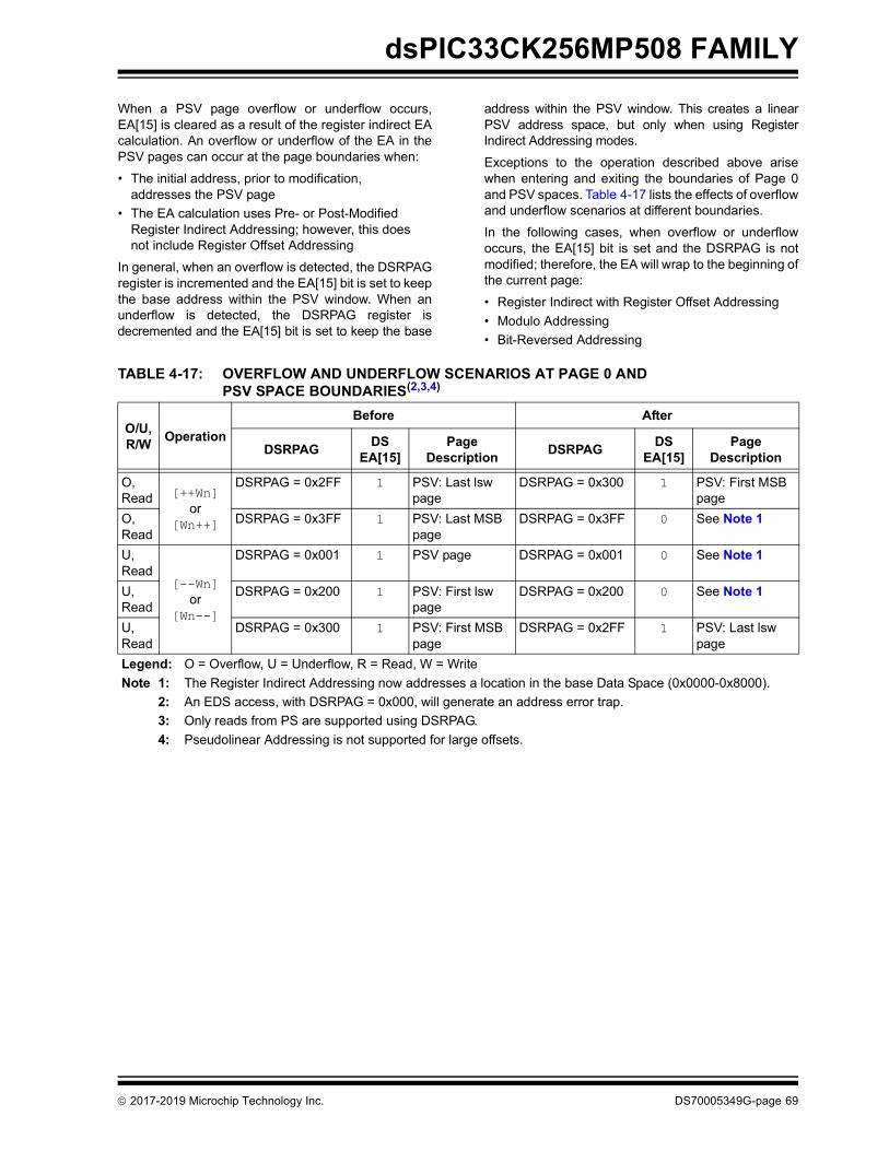
dsPIC33CK256MP508 FAMILY
When a PSV page overflow or underflow occurs,EA[15] is cleared as a result of the register indirect EAcalculation. An overflow or underflow of the EA in thePSV pages can occur at the page boundaries when:• The initial address, prior to modification,
addresses the PSV page• The EA calculation uses Pre- or Post-Modified
Register Indirect Addressing; however, this does not include Register Offset Addressing
In general, when an overflow is detected, the DSRPAGregister is incremented and the EA[15] bit is set to keepthe base address within the PSV window. When anunderflow is detected, the DSRPAG register isdecremented and the EA[15] bit is set to keep the base
address within the PSV window. This creates a linearPSV address space, but only when using RegisterIndirect Addressing modes.Exceptions to the operation described above arisewhen entering and exiting the boundaries of Page 0and PSV spaces. Table 4-17 lists the effects of overflowand underflow scenarios at different boundaries.In the following cases, when overflow or underflowoccurs, the EA[15] bit is set and the DSRPAG is notmodified; therefore, the EA will wrap to the beginning ofthe current page:• Register Indirect with Register Offset Addressing• Modulo Addressing• Bit-Reversed Addressing
TABLE 4-17: OVERFLOW AND UNDERFLOW SCENARIOS AT PAGE 0 AND PSV SPACE BOUNDARIES(2,3,4)
O/U, R/W Operation
Before After
DSRPAG DSEA[15]
Page Description DSRPAG DS
EA[15]Page
Description
O,Read [++Wn]
or[Wn++]
DSRPAG = 0x2FF 1 PSV: Last lsw page
DSRPAG = 0x300 1 PSV: First MSB page
O,Read
DSRPAG = 0x3FF 1 PSV: Last MSB page
DSRPAG = 0x3FF 0 See Note 1
U,Read
[--Wn]or
[Wn--]
DSRPAG = 0x001 1 PSV page DSRPAG = 0x001 0 See Note 1
U,Read
DSRPAG = 0x200 1 PSV: First lsw page
DSRPAG = 0x200 0 See Note 1
U,Read
DSRPAG = 0x300 1 PSV: First MSB page
DSRPAG = 0x2FF 1 PSV: Last lsw page
Legend: O = Overflow, U = Underflow, R = Read, W = WriteNote 1: The Register Indirect Addressing now addresses a location in the base Data Space (0x0000-0x8000).
2: An EDS access, with DSRPAG = 0x000, will generate an address error trap.3: Only reads from PS are supported using DSRPAG.4: Pseudolinear Addressing is not supported for large offsets.
2017-2019 Microchip Technology Inc. DS70005349G-page 69

dsPIC33CK256MP508 FAMILY
4.4.1.1 Extended X Data Space The lower portion of the base address space range,between 0x0000 and 0x7FFF, is always accessible,regardless of the contents of the Data Space ReadPage register. It is indirectly addressable through theregister indirect instructions. It can be regarded asbeing located in the default EDS Page 0 (i.e., EDSaddress range of 0x000000 to 0x007FFF with the baseaddress bit, EA[15] = 0, for this address range). How-ever, Page 0 cannot be accessed through the upper32 Kbytes, 0x8000 to 0xFFFF, of base Data Space incombination with DSRPAG = 0x00. Consequently,DSRPAG is initialized to 0x001 at Reset.
The remaining PSV pages are only accessible usingthe DSRPAG register in combination with the upper32 Kbytes, 0x8000 to 0xFFFF, of the base address,where the base address bit, EA[15] = 1.
4.4.1.2 Software StackThe W15 register serves as a dedicated SoftwareStack Pointer (SSP), and is automatically modified byexception processing, subroutine calls and returns;however, W15 can be referenced by any instruction inthe same manner as all other W registers. This simpli-fies reading, writing and manipulating the Stack Pointer(for example, creating stack frames).
W15 is initialized to 0x1000 during all Resets. Thisaddress ensures that the SSP points to valid RAM in alldsPIC33CK256MP508 devices and permits stack avail-ability for non-maskable trap exceptions. These canoccur before the SSP is initialized by the user software.You can reprogram the SSP during initialization to anylocation within Data Space.The Software Stack Pointer always points to the firstavailable free word and fills the software stack,working from lower toward higher addresses.Figure 4-13 illustrates how it pre-decrements for astack pop (read) and post-increments for a stack push(writes).
When the PC is pushed onto the stack, PC[15:0] arepushed onto the first available stack word, thenPC[22:16] are pushed into the second available stacklocation. For a PC push during any CALL instruction,the MSB of the PC is zero-extended before the push,as shown in Figure 4-13. During exception processing,the MSB of the PC is concatenated with the lower eightbits of the CPU STATUS Register, SR. This allows thecontents of SRL to be preserved automatically duringinterrupt processing.
FIGURE 4-13: CALL STACK FRAME
Note 1: DSRPAG should not be used to accessPage 0. An EDS access with DSRPAGset to 0x000 will generate an addresserror trap.
2: Clearing the DSRPAG in software has noeffect.
Note: To protect against misaligned stackaccesses, W15[0] is fixed to ‘0’ by thehardware.
Note 1: To maintain system Stack Pointer (W15)coherency, W15 is never subject to(EDS) paging, and is therefore, restrictedto an address range of 0x0000 to0xFFFF. The same applies to the W14when used as a Stack Frame Pointer(SFA = 1).
2: As the stack can be placed in, and canaccess X and Y spaces, care must betaken regarding its use, particularly withregard to local automatic variables in a Cdevelopment environment
<Free Word>
PC[15:1]b‘000000000’
015
W15 (before CALL)
W15 (after CALL)
Stac
k G
row
s To
war
dH
ighe
r Add
ress
0x0000
PC[22:16]
CALL SUBR
DS70005349G-page 70 2017-2019 Microchip Technology Inc.

dsPIC33CK256MP508 FAMILY
4.4.2 INSTRUCTION ADDRESSING MODES
The addressing modes shown in Table 4-18 form thebasis of the addressing modes optimized to support thespecific features of individual instructions. Theaddressing modes provided in the MAC class ofinstructions differ from those in the other instructiontypes.
4.4.2.1 File Register InstructionsMost file register instructions use a 13-bit address field(f) to directly address data present in the first8192 bytes of data memory (Near Data Space). Mostfile register instructions employ a Working register, W0,which is denoted as WREG in these instructions. Thedestination is typically either the same file register orWREG (with the exception of the MUL instruction),which writes the result to a register or register pair. TheMOV instruction allows additional flexibility and canaccess the entire Data Space.
4.4.2.2 MCU InstructionsThe three-operand MCU instructions are of the form:Operand 3 = Operand 1 <function> Operand 2where Operand 1 is always a Working register (that is,the addressing mode can only be Register Direct),which is referred to as Wb. Operand 2 can be a Wregister fetched from data memory or a 5-bit literal. Theresult location can either be a W register or a datamemory location. The following addressing modes aresupported by MCU instructions:• Register Direct• Register Indirect• Register Indirect Post-Modified• Register Indirect Pre-Modified• 5-Bit or 10-Bit Literal
TABLE 4-18: FUNDAMENTAL ADDRESSING MODES SUPPORTED
Note: Not all instructions support all theaddressing modes given above. Individ-ual instructions can support differentsubsets of these addressing modes.
Addressing Mode Description
File Register Direct The address of the file register is specified explicitly.Register Direct The contents of a register are accessed directly.Register Indirect The contents of Wn form the Effective Address (EA).Register Indirect Post-Modified The contents of Wn form the EA. Wn is post-modified (incremented
or decremented) by a constant value.Register Indirect Pre-Modified Wn is pre-modified (incremented or decremented) by a signed constant value
to form the EA.Register Indirect with Register Offset (Register Indexed)
The sum of Wn and Wb forms the EA.
Register Indirect with Literal Offset The sum of Wn and a literal forms the EA.
2017-2019 Microchip Technology Inc. DS70005349G-page 71

dsPIC33CK256MP508 FAMILY
4.4.2.3 Move and Accumulator InstructionsMove instructions, and the DSP accumulator class ofinstructions, provide a greater degree of addressingflexibility than other instructions. In addition to theaddressing modes supported by most MCU instructions,move and accumulator instructions also supportRegister Indirect with Register Offset Addressing mode,also referred to as Register Indexed mode.
In summary, the following addressing modes aresupported by move and accumulator instructions:• Register Direct• Register Indirect• Register Indirect Post-Modified• Register Indirect Pre-Modified• Register Indirect with Register Offset (Indexed)• Register Indirect with Literal Offset• 8-Bit Literal• 16-Bit Literal
4.4.2.4 MAC InstructionsThe dual source operand DSP instructions (CLR, ED,EDAC, MAC, MPY, MPY.N, MOVSAC and MSC), also referredto as MAC instructions, use a simplified set of addressingmodes to allow the user application to effectivelymanipulate the Data Pointers through register indirecttables.The two-source operand prefetch registers must bemembers of the set {W8, W9, W10, W11}. For datareads, W8 and W9 are always directed to the X RAGU,and W10 and W11 are always directed to the Y AGU.The Effective Addresses generated (before and aftermodification) must therefore, be valid addresses withinX Data Space for W8 and W9, and Y Data Space forW10 and W11.
In summary, the following addressing modes aresupported by the MAC class of instructions:• Register Indirect• Register Indirect Post-Modified by 2• Register Indirect Post-Modified by 4• Register Indirect Post-Modified by 6• Register Indirect with Register Offset (Indexed)
4.4.2.5 Other InstructionsBesides the addressing modes outlined previously,some instructions use literal constants of various sizes.For example, BRA (branch) instructions use 16-bitsigned literals to specify the branch destination directly,whereas the DISI instruction uses a 14-bit unsignedliteral field. In some instructions, such as ULNK, thesource of an operand or result is implied by the opcodeitself. Certain operations, such as a NOP, do not haveany operands.
Note: For the MOV instructions, the addressingmode specified in the instruction can differfor the source and destination EA. How-ever, the 4-bit Wb (Register Offset) field isshared by both source and destination (buttypically only used by one).
Note: Not all instructions support all theaddressing modes given above. Individualinstructions may support different subsetsof these addressing modes.
Note: Register Indirect with Register OffsetAddressing mode is available only for W9(in X space) and W11 (in Y space).
DS70005349G-page 72 2017-2019 Microchip Technology Inc.

dsPIC33CK256MP508 FAMILY
4.4.3 MODULO ADDRESSING Modulo Addressing mode is a method of providing anautomated means to support circular data buffers usinghardware. The objective is to remove the need forsoftware to perform data address boundary checkswhen executing tightly looped code, as is typical inmany DSP algorithms.Modulo Addressing can operate in either Data orProgram Space (since the Data Pointer mechanism isessentially the same for both). One circular buffer can besupported in each of the X (which also provides the point-ers into Program Space) and Y Data Spaces. ModuloAddressing can operate on any W Register Pointer. How-ever, it is not advisable to use W14 or W15 for ModuloAddressing since these two registers are used as theStack Frame Pointer and Stack Pointer, respectively. In general, any particular circular buffer can be config-ured to operate in only one direction, as there are certainrestrictions on the buffer start address (for incrementingbuffers) or end address (for decrementing buffers),based upon the direction of the buffer. The only exception to the usage restrictions is forbuffers that have a power-of-two length. As thesebuffers satisfy the start and end address criteria, theycan operate in a Bidirectional mode (that is, addressboundary checks are performed on both the lower andupper address boundaries).
4.4.3.1 Start and End AddressThe Modulo Addressing scheme requires that astarting and ending address be specified and loadedinto the 16-bit Modulo Buffer Address registers:XMODSRT, XMODEND, YMODSRT and YMODEND(see Table 4-2).
The length of a circular buffer is not directly specified. It isdetermined by the difference between the correspondingstart and end addresses. The maximum possible length ofthe circular buffer is 32K words (64 Kbytes).
4.4.3.2 W Address Register SelectionThe Modulo and Bit-Reversed Addressing Controlregister, MODCON[15:0], contains enable flags, as wellas a W register field to specify the W Address registers.The XWM and YWM fields select the registers thatoperate with Modulo Addressing:• If XWM = 1111, X RAGU and X WAGU Modulo
Addressing is disabled• If YWM = 1111, Y AGU Modulo Addressing is
disabledThe X Address Space Pointer W (XWM) register, towhich Modulo Addressing is to be applied, is stored inMODCON[3:0] (see Table 4.2). Modulo Addressing isenabled for X Data Space when XWM is set to anyvalue other than ‘1111’ and the XMODEN bit is set(MODCON[15]).The Y Address Space Pointer W (YWM) register, towhich Modulo Addressing is to be applied, is stored inMODCON[7:4]. Modulo Addressing is enabled forY Data Space when YWM is set to any value other than‘1111’ and the YMODEN bit (MODCON[14]) is set.
FIGURE 4-14: MODULO ADDRESSING OPERATION EXAMPLE
Note: Y space Modulo Addressing EA calcula-tions assume word-sized data (LSb ofevery EA is always clear).
0x1100
0x1163
Start Addr = 0x1100End Addr = 0x1163Length = 0x0032 words
ByteAddress
MOV #0x1100, W0MOV W0, XMODSRT ;set modulo start addressMOV #0x1163, W0MOV W0, MODEND ;set modulo end addressMOV #0x8001, W0MOV W0, MODCON ;enable W1, X AGU for modulo
MOV #0x0000, W0 ;W0 holds buffer fill value
MOV #0x1110, W1 ;point W1 to buffer
DO AGAIN, #0x31 ;fill the 50 buffer locationsMOV W0, [W1++] ;fill the next locationAGAIN: INC W0, W0 ;increment the fill value
2017-2019 Microchip Technology Inc. DS70005349G-page 73

dsPIC33CK256MP508 FAMILY
4.4.3.3 Modulo Addressing ApplicabilityModulo Addressing can be applied to the EffectiveAddress (EA) calculation associated with any Wregister. Address boundaries check for addressesequal to:• The upper boundary addresses for incrementing
buffers• The lower boundary addresses for decrementing
buffersIt is important to realize that the address boundariescheck for addresses less than, or greater than, theupper (for incrementing buffers) and lower (for decre-menting buffers) boundary addresses (not just equalto). Address changes can, therefore, jump beyondboundaries and still be adjusted correctly.
4.4.4 BIT-REVERSED ADDRESSINGBit-Reversed Addressing mode is intended to simplifydata reordering for radix-2 FFT algorithms. It issupported by the X AGU for data writes only.The modifier, which can be a constant value or registercontents, is regarded as having its bit order reversed.The address source and destination are kept in normalorder. Thus, the only operand requiring reversal is themodifier.
4.4.4.1 Bit-Reversed Addressing Implementation
Bit-Reversed Addressing mode is enabled in any ofthese situations:• BWMx bits (W register selection) in the MODCON
register are any value other than ‘1111’ (the stack cannot be accessed using Bit-Reversed Addressing)
• The BREN bit is set in the XBREV register• The addressing mode used is Register Indirect
with Pre-Increment or Post-IncrementIf the length of a bit-reversed buffer is M = 2N bytes,the last ‘N’ bits of the data buffer start address mustbe zeros. XB[14:0] is the Bit-Reversed Addressing modifier, or‘pivot point’, which is typically a constant. In the case ofan FFT computation, its value is equal to half of the FFTdata buffer size.
When enabled, Bit-Reversed Addressing is executedonly for Register Indirect with Pre-Increment or Post-Increment Addressing and word-sized data writes. Itdoes not function for any other addressing mode or forbyte-sized data and normal addresses are generatedinstead. When Bit-Reversed Addressing is active, theW Address Pointer is always added to the addressmodifier (XB) and the offset associated with theRegister Indirect Addressing mode is ignored. In addi-tion, as word-sized data are a requirement, the LSb ofthe EA is ignored (and always clear).
If Bit-Reversed Addressing has already been enabledby setting the BREN (XBREV[15]) bit, a write to theXBREV register should not be immediately followed byan indirect read operation using the W register that hasbeen designated as the Bit-Reversed Pointer.
Note: The modulo corrected Effective Addressis written back to the register only whenPre-Modify or Post-Modify Addressingmode is used to compute the EffectiveAddress. When an address offset (such as[W7 + W2]) is used, Modulo Addressingcorrection is performed, but the contents ofthe register remain unchanged.
Note: All bit-reversed EA calculations assumeword-sized data (LSb of every EA isalways clear). The XB value is scaledaccordingly to generate compatible (byte)addresses.
Note: Modulo Addressing and Bit-ReversedAddressing can be enabled simultaneouslyusing the same W register, but Bit-Reversed Addressing operation will alwaystake precedence for data writes whenenabled.
DS70005349G-page 74 2017-2019 Microchip Technology Inc.

dsPIC33CK256MP508 FAMILY
FIGURE 4-15: BIT-REVERSED ADDRESSING EXAMPLE
TABLE 4-19: BIT-REVERSED ADDRESSING SEQUENCE (16-ENTRY)Normal Address Bit-Reversed Address
A3 A2 A1 A0 Decimal A3 A2 A1 A0 Decimal
0 0 0 0 0 0 0 0 0 00 0 0 1 1 1 0 0 0 80 0 1 0 2 0 1 0 0 40 0 1 1 3 1 1 0 0 120 1 0 0 4 0 0 1 0 20 1 0 1 5 1 0 1 0 100 1 1 0 6 0 1 1 0 60 1 1 1 7 1 1 1 0 141 0 0 0 8 0 0 0 1 11 0 0 1 9 1 0 0 1 91 0 1 0 10 0 1 0 1 51 0 1 1 11 1 1 0 1 131 1 0 0 12 0 0 1 1 31 1 0 1 13 1 0 1 1 111 1 1 0 14 0 1 1 1 71 1 1 1 15 1 1 1 1 15
b3 b2 b1 0
b2 b3 b4 0
Bit Locations Swapped Left-to-RightAround Center of Binary Value
Bit-Reversed Address
XB = 0x0008 for a 16-Word Bit-Reversed Buffer
b7 b6 b5 b1
b7 b6 b5 b4b11 b10 b9 b8
b11 b10 b9 b8
b15 b14 b13 b12
b15 b14 b13 b12
Sequential Address
Pivot Point
2017-2019 Microchip Technology Inc. DS70005349G-page 75

dsPIC33CK256MP508 FAMILY
4.4.5 INTERFACING PROGRAM AND DATA MEMORY SPACES
The dsPIC33CK256MP508 family architecture uses a24-bit wide Program Space (PS) and a 16-bit wide DataSpace (DS). The architecture is also a modifiedHarvard scheme, meaning that data can also bepresent in the Program Space. To use this data suc-cessfully, it must be accessed in a way that preservesthe alignment of information in both spaces.Aside from normal execution, the architecture ofthe dsPIC33CK256MP508 family devices providestwo methods by which Program Space can beaccessed during operation: • Using table instructions to access individual bytes
or words anywhere in the Program Space• Remapping a portion of the Program Space into
the Data Space (Program Space Visibility)
Table instructions allow an application to read or writeto small areas of the program memory. This capabilitymakes the method ideal for accessing data tables thatneed to be updated periodically. It also allows accessto all bytes of the program word. The remappingmethod allows an application to access a large block ofdata on a read-only basis, which is ideal for look-upsfrom a large table of static data. The application canonly access the least significant word of the programword.
TABLE 4-20: PROGRAM SPACE ADDRESS CONSTRUCTION
FIGURE 4-16: DATA ACCESS FROM PROGRAM SPACE ADDRESS GENERATION
Access Type AccessSpace
Program Space Address[23] [22:16] [15] [14:1] [0]
Instruction Access(Code Execution)
User 0 PC[22:1] 00xxx xxxx xxxx xxxx xxxx xxx0
TBLRD/TBLWT(Byte/Word Read/Write)
User TBLPAG[7:0] Data EA[15:0]0xxx xxxx xxxx xxxx xxxx xxxx
Configuration TBLPAG[7:0] Data EA[15:0]1xxx xxxx xxxx xxxx xxxx xxxx
0Program Counter
23 Bits
Program Counter(1)
TBLPAG
8 Bits
EA
16 Bits
Byte Select
0
1/0
User/Configuration
Table Operations(2)
Space Select
24 Bits
1/0
Note 1: The Least Significant bit (LSb) of Program Space addresses is always fixed as ‘0’ to maintain word alignment of data in the Program and Data Spaces.
2: Table operations are not required to be word-aligned. Table Read operations are permitted in the configuration memory space.
DS70005349G-page 76 2017-2019 Microchip Technology Inc.

dsPIC33CK256MP508 FAMILY
4.4.5.1 Data Access from Program Memory Using Table Instructions
The TBLRDL and TBLWTL instructions offer a directmethod of reading or writing the lower word of anyaddress within the Program Space without goingthrough Data Space. The TBLRDH and TBLWTHinstructions are the only method to read or write theupper 8 bits of a Program Space word as data.The PC is incremented by two for each successive24-bit program word. This allows program memoryaddresses to directly map to Data Space addresses.Program memory can thus be regarded as two 16-bitwide word address spaces, residing side by side, eachwith the same address range. TBLRDL and TBLWTLaccess the space that contains the least significantdata word. TBLRDH and TBLWTH access the space thatcontains the upper data byte. Two table instructions are provided to move byte orword-sized (16-bit) data to and from Program Space.Both function as either byte or word operations.• TBLRDL (Table Read Low):
- In Word mode, this instruction maps the lower word of the Program Space location (P[15:0]) to a data address (D[15:0])
- In Byte mode, either the upper or lower byte of the lower program word is mapped to the lower byte of a data address. The upper byte is selected when Byte Select is ‘1’; the lower byte is selected when it is ‘0’.
• TBLRDH (Table Read High):- In Word mode, this instruction maps the entire
upper word of a program address (P[23:16]) to a data address. The ‘phantom’ byte (D[15:8]) is always ‘0’.
- In Byte mode, this instruction maps the upper or lower byte of the program word to D[7:0] of the data address in the TBLRDL instruction. The data are always ‘0’ when the upper ‘phantom’ byte is selected (Byte Select = 1).
In a similar fashion, two table instructions, TBLWTHand TBLWTL, are used to write individual bytes orwords to a Program Space address. The details oftheir operation are explained in Section 5.0 “FlashProgram Memory”.For all table operations, the area of program memoryspace to be accessed is determined by the Table Pageregister (TBLPAG). TBLPAG covers the entire programmemory space of the device, including user applicationand configuration spaces. When TBLPAG[7] = 0, thetable page is located in the user memory space. WhenTBLPAG[7] = 1, the page is located in configurationspace.
FIGURE 4-17: ACCESSING PROGRAM MEMORY WITH TABLE INSTRUCTIONS
0816230000000000000000
0000000000000000
‘Phantom’ Byte
TBLRDH.B (Wn[0] = 0)
TBLRDL.W
TBLRDL.B (Wn[0] = 1)TBLRDL.B (Wn[0] = 0)
23 15 0
TBLPAG02
0x000000
0x800000
0x020000
0x030000
Program Space
The address for the table operation is determined by the data EAwithin the page defined by the TBLPAG register. Only read operations are shown; write operations are also valid inthe user memory area.
2017-2019 Microchip Technology Inc. DS70005349G-page 77

dsPIC33CK256MP508 FAMILY
NOTES:
DS70005349G-page 78 2017-2019 Microchip Technology Inc.

dsPIC33CK256MP508 FAMILY
5.0 FLASH PROGRAM MEMORY
The dsPIC33CK256MP508 family devices containinternal Flash program memory for storing andexecuting application code. The memory is readable,writable and erasable during normal operation over theentire VDD range.Flash memory can be programmed in three ways:• In-Circuit Serial Programming™ (ICSP™)
programming capability• Enhanced In-Circuit Serial Programming
(Enhanced ICSP)• Run-Time Self-Programming (RTSP)ICSP allows for a dsPIC33CK256MP508 family deviceto be serially programmed while in the end applicationcircuit. This is done with a Programming Clock and Pro-gramming Data (PGCx/PGDx) line, and three otherlines for power (VDD), ground (VSS) and Master Clear(MCLR). This allows customers to manufacture boardswith unprogrammed devices and then program the
device just before shipping the product. This alsoallows the most recent firmware or a custom firmwareto be programmed.Enhanced In-Circuit Serial Programming uses anon-board bootloader, known as the Program Executive,to manage the programming process. Using an SPI dataframe format, the Program Executive can erase,program and verify program memory. For more informa-tion on Enhanced ICSP, see the device programmingspecification.RTSP is accomplished using TBLRD (Table Read) andTBLWT (Table Write) instructions. With RTSP, the userapplication can write program memory data, twoinstruction words or a row at a time, and erase aprogram memory page.
5.1 Table Instructions and Flash Programming
Regardless of the method used, all programming ofFlash memory is done with the Table Read and TableWrite instructions. These allow direct read and writeaccess to the program memory space from the datamemory while the device is in normal operating mode.The 24-bit target address in the program memory isformed using bits[7:0] of the TBLPAG register and theEffective Address (EA) from a W register, specified inthe table instruction, as shown in Figure 5-1. TheTBLRDL and TBLWTL instructions are used to read orwrite to bits[15:0] of program memory. TBLRDL andTBLWTL can access program memory in both Wordand Byte modes. The TBLRDH and TBLWTHinstructions are used to read or write to bits[23:16] ofprogram memory. TBLRDH and TBLWTH can alsoaccess program memory in Word or Byte mode.
FIGURE 5-1: ADDRESSING FOR TABLE REGISTERS
Note 1: This data sheet summarizes the features ofthe dsPIC33CK256MP508 family of devices.It is not intended to be a comprehensivereference source. To complement theinformation in this data sheet, refer to“Dual Partition Flash Program Memory”(www.microchip.com/DS70005156) in the“dsPIC33/PIC24 Family ReferenceManual”).
2: Some registers and associated bitsdescribed in this section may not beavailable on all devices.
0Program Counter
24 Bits
Program Counter
TBLPAG Reg
8 Bits
Working Reg EA
16 Bits
Byte24-Bit EA
0
1/0
Select
UsingTable Instruction
Using
User/ConfigurationSpace Select
2017-2019 Microchip Technology Inc. DS70005349G-page 79

dsPIC33CK256MP508 FAMILY
5.2 RTSP OperationThe dsPIC33CK256MP508 family Flash programmemory array is organized into rows of 128 instructionsor 384 bytes. RTSP allows the user application to erase asingle page (eight rows or 1024 instructions) of memoryat a time and to program one row at a time. It is possibleto program two instructions at a time as well.The page erase and single row write blocks areedge-aligned, from the beginning of programmemory, on boundaries of 3072 bytes and 384 bytes,respectively. Table 33-18 in Section 33.0 “Electri-cal Characteristics” lists the typical erase andprogramming times.Row programming is performed by loading 384 bytesinto data memory and then loading the address of thefirst byte in that row into the NVMSRCADRL/H register.Once the write has been initiated, the device willautomatically load the write latches, and increment theNVMSRCADRL/H and the NVMADR(U) registers untilall bytes have been programmed. The RPDF bit(NVMCON[9]) selects the format of the stored data inRAM to be either compressed or uncompressed. SeeFigure 5-2 for data formatting. Compressed data helpto reduce the amount of required RAM by using theupper byte of the second word for the MSB of thesecond instruction. The basic sequence for RTSP word programming is touse the TBLWTL and TBLWTH instructions to load two ofthe 24-bit instructions into the write latches found inconfiguration memory space. Refer to Figure 4-1through Figure 4-5 for write latch addresses. Program-ming is performed by unlocking and setting the controlbits in the NVMCON register as follows:1. Write 0x55 to NVMKEY.2. Write 0xAA to NVMKEY.3. Set the WR bit (NVMCON[15]) as a single
operation.
All erase and program operations may optionally usethe NVM interrupt to signal the successful completionof the operation. For example, when performing Flashwrite operations on the Inactive Partition in DualPartition mode, where the CPU remains running, it isnecessary to wait for the NVM interrupt beforeprogramming the next block of Flash program memory.
FIGURE 5-2: UNCOMPRESSED/COMPRESSED FORMAT
Note: MPLAB® XC16 provides a built-in Clanguage function for unlocking andmodifying the NVMCON register:__builtin_write_NVM()For more information, see the “MPLAB®
XC16 C Compiler User’s Guide”(DS50002071).
MSB10x00
LSW2
LSW1
Incr
easi
ngAd
dres
s
0715Even ByteAddress
MSB20x00
MSB1MSB2
LSW2
LSW1
Incr
easi
ngAd
dres
s
0715Even ByteAddress
UNCOMPRESSED FORMAT (RPDF = 0)
COMPRESSED FORMAT (RPDF = 1)
DS70005349G-page 80 2017-2019 Microchip Technology Inc.

dsPIC33CK256MP508 FAMILY
5.3 Programming OperationsA complete programming sequence is necessary forprogramming or erasing the internal Flash in RTSPmode. The processor stalls (waits) until the pro-gramming operation is finished. Setting the WR bit(NVMCON[15]) starts the operation and the WR bit isautomatically cleared when the operation is finished.
5.3.1 PROGRAMMING ALGORITHM FOR FLASH PROGRAM MEMORY
Programmers can program two adjacent words(24 bits x 2) of Program Flash Memory at a time onevery other word address boundary (0x000002,
0x000006, 0x00000A, etc.). To do this, it is necessary toerase the page that contains the desired address of thelocation the user wants to change. For protection againstaccidental operations, the write initiate sequence forNVMKEY must be used to allow any erase or programoperation to proceed. After the programming commandhas been executed, the user application must wait forthe programming time until programming is complete.The two instructions following the start of theprogramming sequence should be NOPs. Refer toExample 5-1 for Flash read and write operations.
EXAMPLE 5-1: FLASH WRITE/READ/////////Flash write //////////////////////////Sample code for writing 0x123456 to address locations 0x10000 / 10002NVMCON = 0x4001;TBLPAG = 0xFA; // write latch upper addressNVMADR = 0x0000; // set target write address of general segmentNVMADRU = 0x0001;__builtin_tblwtl(0, 0x3456); // load write latches__builtin_tblwth (0,0x12);
__builtin_tblwtl(2, 0x3456); // load write latches__builtin_tblwth (2,0x12);
asm volatile ("disi #5");__builtin_write_NVM();while(_WR == 1 ) ;////////////Flash Read/////////////////Sample code to read the Flash content of address 0x10000// readDataL/ readDataH variables need to definedTBLPAG = 0x0001;readDataL = __builtin_tblrdl(0x0000);readDataH = __builtin_tblrdh(0x0000);
2017-2019 Microchip Technology Inc. DS70005349G-page 81

dsPIC33CK256MP508 FAMILY
5.3.2 ERROR CORRECTING CODE (ECC)In order to improve program memory performance anddurability, these devices include Error Correcting Code(ECC) functionality as an integral part of the Flashmemory controller. ECC can determine the presence ofsingle bit errors in program data, including which bit isin error, and correct the data automatically without userintervention. ECC cannot be disabled. When data are written to program memory, ECCgenerates a 7-bit Hamming code parity value for everytwo (24-bit) instruction words. The data are stored inblocks of 48 data bits and 7 parity bits; parity data arenot memory-mapped and are inaccessible. When thedata are read back, the ECC calculates the parity onthem and compares them to the previously storedparity value. If a parity mismatch occurs, there are twopossible outcomes:• Single bit error has occurred and has been
automatically corrected on read-back. • Double-bit error has occurred and the read data
are not changed.Single bit error occurrence can be identified by thestate of the ECCSBEIF (IFS0[13]) bit. An interrupt canbe generated when the corresponding interrupt enablebit is set, ECCSBEIE (IEC0[13]). The ECCSTATLregister contains the parity information for single biterrors. The SECOUT[7:0] bits field contains theexpected calculated SEC parity and the SECIN[7:0]bits contain the actual value from a Flash read opera-tion. The SECSYNDx bits (ECCSTATH[7:0]) indicatethe bit position of the single bit error within the 48-bitpair of instruction words. When no error is present,SECINx equals SECOUTx and SECSYNDx is zero.Double-bit errors result in a generic hard trap. TheECCDBE bit (INTCON4[1]) will be set to identify thesource of the hard trap. If no Interrupt Service Routineis implemented for the hard trap, a device Reset willalso occur. The ECCSTATH register contains double-bit error status information. The DEDOUT bit is theexpected calculated DED parity and DEDIN is theactual value from a Flash read operation. When noerror is present, DEDIN equals DEDOUT.
5.3.3 ECC FAULT INJECTIONTo test Fault handling, an EEC error can be generated.Both single and double-bit errors can be generated inboth the read and write data paths. Read path Faultinjection first reads the Flash data and then modifiesthem prior to entering the ECC logic. Write path Faultinjection modifies the actual data prior to them beingwritten into the target Flash and will cause an EEC erroron a subsequent Flash read. The following procedureis used to inject a Fault:1. Load the Flash target address into the
ECCADDR register. 2. Select 1st Fault bit determined by FLT1PTRx
(ECCCONH[7:0]). The target bit is inverted tocreate the Fault.
3. If a double Fault is desired, select the 2nd Fault bitdetermined by FLT2PTRx (ECCCONH[15:8]);otherwise, set to all ‘1’s.
4. Write 0x55 to NVMKEY.5. Write 0xAA to NVMKEY.6. Set the FLTINJ bit (ECCCONL[0]) in a single
operation to enable the ECC Fault injectionlogic.
7. Perform a read or write to the Flash targetaddress.
DS70005349G-page 82 2017-2019 Microchip Technology Inc.

dsPIC33CK256MP508 FAMILY
5.4 ICSP™ Write InhibitICSP Write Inhibit is an access restriction feature that,when activated, restricts all of Flash memory. Once acti-vated, ICSP Write Inhibit permanently prevents ICSPFlash programming and erase operations, and cannotbe deactivated. This feature is intended to preventalteration of Flash memory contents, with behaviorsimilar to One-Time-Programmable (OTP) devices.RTSP, including erase and programming operations, isnot restricted when ICSP Write Inhibit is activated;however, code to perform these actions must be pro-grammed into the device before ICSP Write Inhibit isactivated. This allows for a bootloader-type applicationto alter Flash contents with ICSP Write Inhibit activated.Entry into ICSP and Enhanced ICSP modes is notaffected by ICSP Write Inhibit. In these modes, it willcontinue to be possible to read configuration memoryspace and any user memory space regions which arenot code protected. With ICSP writes inhibited, anattempt to set WR (NVMCON[15]) = 1 will maintainWR = 0, and instead, set WRERR (NVMCON[13]) = 1.All Enhanced ICSP erase and programming commandswill have no effect with self-checked programmingcommands returning a FAIL response opcode (PASS ifthe destination already exactly matched the requestedprogramming data).Once ICSP Write Inhibit is activated, it is not possible fora device executing in Debug mode to erase/write Flash,nor can a debug tool switch the device to Productionmode. ICSP Write Inhibit should therefore only beactivated on devices programmed for production.The JTAG port, when enabled, can be used to mapICSP signals to JTAG I/O pins. All Flash erase/programming operations initiated via the JTAG port willtherefore also be blocked after activating ICSP WriteInhibit.
5.4.1 ACTIVATING ICSP™ WRITE INHIBIT
ICSP Write Inhibit is activated by executing a pair ofNVMCON double-word programming commands to savetwo 16-bit activation values in the configuration memoryspace. The target NVM addresses and values requiredfor activation are shown in Table 5-1. Once bothaddresses contain their activation values, ICSP WriteInhibit will take permanent effect on the next deviceReset. Neither address can be reset, erased or otherwisemodified, through any means, after being successfullyprogrammed, even if one of the addresses has not beenprogrammed.
Only the lower 16 data bits stored at the activationaddresses are evaluated; the upper 8 bits and second24-bit word written by the double-word programming(NVMOP[3:0]) should be written as ‘0’s. The addressescan be programmed in any order and also during sepa-rate ICSP/Enhanced ICSP/RTSP sessions, but anyattempt to program an incorrect 16-bit value or use a rowprogramming operation to program the values will beaborted without altering the existing data.
TABLE 5-1: ICSP™ WRITE INHIBIT ACTIVATION ADDRESSES AND DATA
Caution: It is not possible to deactivate ICSPWrite Inhibit.
Configuration Memory Address
ICSP™ Write Inhibit Activation
Value
Write Lock 1 0x801034 0x006D63Write Lock 2 0x801038 0x006870
2017-2019 Microchip Technology Inc. DS70005349G-page 83

dsPIC33CK256MP508 FAMILY
5.5 Dual Partition Flash ConfigurationFor dsPIC33CK256MP508 devices operating in DualPartition Flash Program Memory modes, the InactivePartition can be erased and programmed without stall-ing the processor. The same programming algorithmsare used for programming and erasing the Flash in theInactive Partition, as described in Section 5.2 “RTSPOperation”. On top of the page erase option, the entireFlash memory of the Inactive Partition can be erasedby configuring the NVMOP[3:0] bits in the NVMCONregister.
5.5.1 FLASH PARTITION SWAPPINGThe Boot Sequence Number is used for determiningthe Active Partition at start-up and is encoded withinthe FBTSEQ Configuration register bits. Unlike mostConfiguration registers, which only utilize the lower16 bits of the program memory, FBTSEQ is a 24-bitConfiguration Word. The Boot Sequence Number(BSEQ) is a 12-bit value and is stored in FBTSEQtwice. The true value is stored in bits, FBTSEQ[11:0],and its complement is stored in bits, FBTSEQ[23:12].At device Reset, the sequence numbers are read andthe partition with the lowest sequence numberbecomes the Active Partition. If one of the BootSequence Numbers is invalid, the device will select thepartition with the valid Boot Sequence Number, ordefault to Partition 1 if both sequence numbers areinvalid. See Section 30.0 “Special Features” for moreinformation. The BOOTSWP instruction provides an alternativemeans of swapping the Active and Inactive Partitions(soft swap) without the need for a device Reset. TheBOOTSWP must always be followed by a GOTO instruc-tion. The BOOTSWP instruction swaps the Active andInactive Partitions, and the PC vectors to the locationspecified by the GOTO instruction in the newly ActivePartition.It is important to note that interrupts should temporarilybe disabled while performing the soft swap sequenceand that after the partition swap, all peripherals andinterrupts which were enabled remain enabled. Addi-tionally, the RAM and stack will maintain state after theswitch. As a result, it is recommended that applicationsusing soft swaps jump to a routine that will reinitializethe device in order to ensure the firmware runs asexpected. The Configuration registers will have noeffect during a soft swap.
For robustness of operation, in order to execute theBOOTSWP instruction, it is necessary to execute theNVM unlocking sequence as follows:1. Write 0x55 to NVMKEY.2. Write 0xAA to NVMKEY.3. Execute the BOOTSWP instruction.If the unlocking sequence is not performed, theBOOTSWP instruction will be executed as a forced NOPand a GOTO instruction, following the BOOTSWP instruc-tion, will be executed, causing the PC to jump to thatlocation in the current operating partition. The SFTSWP and P2ACTIV bits in the NVMCONregister are used to determine a successful swap of theActive and Inactive Partitions, as well as which partitionis active. After the BOOTSWP and GOTO instructions, theSFTSWP bit should be polled to verify the partitionswap has occurred and then cleared for the next panelswap event.
5.5.2 DUAL PARTITION MODESWhile operating in Dual Partition mode, thedsPIC33CK256MP508 family devices have the optionfor both partitions to have their own defined securitysegments, as shown in Figure 30-4. Alternatively, thedevice can operate in Protected Dual Partition mode,where Partition 1 becomes permanently erase/write-protected. Protected Dual Partition mode allows for a“Factory Default” mode, which provides a fail-safebackup image to be stored in Partition 1.dsPIC33CK256MP508 family devices can also operatein Privileged Dual Partition mode, where additionalsecurity protections are implemented to allow for pro-tection of intellectual property when multiple partieshave software within the device. In Privileged Dual Par-tition mode, both partitions place additional restrictionson the FBSLIM register. These prevent changes to thesize of the Boot Segment and General Segment,ensuring that neither segment will be altered.
Note 1: The application software to be loadedinto the Inactive Partition will have theaddress of the Active Partition. Thebootloader firmware will need to offsetthe address by 0x400000 in order to writeto the Inactive Partition.
DS70005349G-page 84 2017-2019 Microchip Technology Inc.
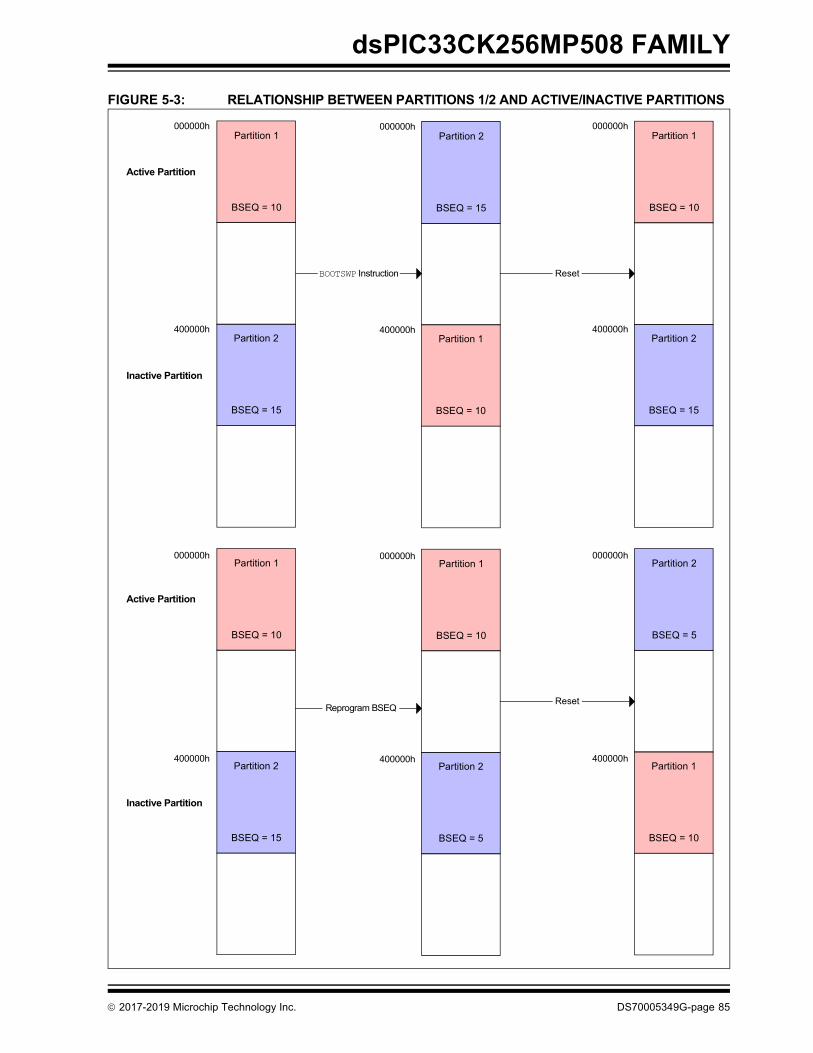
dsPIC33CK256MP508 FAMILY
FIGURE 5-3: RELATIONSHIP BETWEEN PARTITIONS 1/2 AND ACTIVE/INACTIVE PARTITIONS
Active Partition
Active Partition
Inactive Partition
Inactive Partition
Partition 1
BSEQ = 10
Partition 2
BSEQ = 15
Partition 2
BSEQ = 15
Partition 1
BSEQ = 10
Partition 1
BSEQ = 10
Partition 2
BSEQ = 15
Partition 1
BSEQ = 10
Partition 2
BSEQ = 15
Partition 1
BSEQ = 10
Partition 2
BSEQ = 5
Partition 2
BSEQ = 5
Partition 1
BSEQ = 10
000000h
400000h
000000h
400000h
000000h
400000h
000000h
400000h
000000h
400000h
000000h
400000h
ResetBOOTSWP Instruction
Reprogram BSEQReset
2017-2019 Microchip Technology Inc. DS70005349G-page 85

dsPIC33CK256MP508 FAMILY
5.5.3 PROGRAM FLASH MEMORY CONTROL REGISTERS
Five SFRs are used to write and erase the ProgramFlash Memory: NVMCON, NVMKEY, NVMADR,NVMADRU and NVMSRCADRL/H.The NVMCON register (Register 5-1) selects theoperation to be performed (page erase, word/rowprogram, Inactive Partition erase) and initiates theprogram or erase cycle. NVMKEY (Register 5-4) is a write-only register that isused for write protection. To start a programming or erasesequence, the user application must consecutively write0x55 and 0xAA to the NVMKEY register.
There are two NVM Address registers: NVMADRU andNVMADR. These two registers, when concatenated,form the 24-bit Effective Address (EA) of the selectedword/row for programming operations, or the selectedpage for erase operations. The NVMADRU register isused to hold the upper eight bits of the EA, while theNVMADR register is used to hold the lower 16 bits ofthe EA.For row programming operation, data to be written toProgram Flash Memory are written into data memoryspace (RAM) at an address defined by theNVMSRCADRL/H register (location of first element inrow programming data).
DS70005349G-page 86 2017-2019 Microchip Technology Inc.

dsPIC33CK256MP508 FAMILY
REGISTER 5-1: NVMCON: NONVOLATILE MEMORY (NVM) CONTROL REGISTER
R/SO-0(1) R/W-0(1) R/W-0(1) R/W-0 R/C-0 R-0 R/W-0 R/C-0WR WREN WRERR NVMSIDL(2) SFTSWP P2ACTIV RPDF URERR
bit 15 bit 8
U-0 U-0 U-0 U-0 R/W-0(1) R/W-0(1) R/W-0(1) R/W-0(1)
— — — — NVMOP3(3,4) NVMOP2(3,4) NVMOP1(3,4) NVMOP0(3,4)
bit 7 bit 0
Legend: C = Clearable bit SO = Settable Only bitR = Readable bit W = Writable bit U = Unimplemented bit, read as ‘0’-n = Value at POR ‘1’ = Bit is set ‘0’ = Bit is cleared x = Bit is unknown
bit 15 WR: Write Control bit(1)
1 = Initiates a Flash memory program or erase operation; the operation is self-timed and the bit iscleared by hardware once the operation is complete
0 = Program or erase operation is complete and inactivebit 14 WREN: Write Enable bit(1)
1 = Enables Flash program/erase operations0 = Inhibits Flash program/erase operations
bit 13 WRERR: Write Sequence Error Flag bit(1)
1 = An improper program or erase sequence attempt, or termination has occurred (bit is set automaticallyon any set attempt of the WR bit)
0 = The program or erase operation completed normallybit 12 NVMSIDL: NVM Stop in Idle Control bit(2)
1 = Flash voltage regulator goes into Standby mode during Idle mode0 = Flash voltage regulator is active during Idle mode
bit 11 SFTSWP: Partition Soft Swap Status bit1 = Partitions have been successfully swapped using the BOOTSWP instruction (soft swap)0 = Awaiting successful partition swap using the BOOTSWP instruction or a device Reset will determine
the Active Partition based on the FBTSEQ registerbit 10 P2ACTIV: Partition 2 Active Status bit
1 = Partition 2 Flash is mapped into the active region0 = Partition 1 Flash is mapped into the active region
bit 9 RPDF: Row Programming Data Format bit1 = Row data to be stored in RAM are in compressed format0 = Row data to be stored in RAM are in uncompressed format
bit 8 URERR: Row Programming Data Underrun Error bit1 = Indicates row programming operation has been terminated0 = No data underrun error is detected
bit 7-4 Unimplemented: Read as ‘0’
Note 1: These bits can only be reset on a POR.2: If this bit is set, there will be minimal power savings (IIDLE), and upon exiting Idle mode, there is a delay
(TVREG) before Flash memory becomes operational.3: All other combinations of NVMOP[3:0] are unimplemented.4: Execution of the PWRSAV instruction is ignored while any of the NVM operations are in progress.5: Two adjacent words on a 4-word boundary are programmed during execution of this operation.
2017-2019 Microchip Technology Inc. DS70005349G-page 87

dsPIC33CK256MP508 FAMILY
bit 3-0 NVMOP[3:0]: NVM Operation Select bits(1,3,4)
1111 = Reserved1110 = User memory bulk erase operation1101 = Reserved1100 = Reserved1011 = Reserved1010 = Reserved1001 = Reserved1000 = Boot mode (FBOOT) double-word program operation0111 = Reserved0101 = Reserved0100 = Inactive Partition memory erase operation0011 = Memory page erase operation0010 = Memory row program operation0001 = Memory double-word operation(5)
0000 = Reserved
REGISTER 5-1: NVMCON: NONVOLATILE MEMORY (NVM) CONTROL REGISTER (CONTINUED)
Note 1: These bits can only be reset on a POR.2: If this bit is set, there will be minimal power savings (IIDLE), and upon exiting Idle mode, there is a delay
(TVREG) before Flash memory becomes operational.3: All other combinations of NVMOP[3:0] are unimplemented.4: Execution of the PWRSAV instruction is ignored while any of the NVM operations are in progress.5: Two adjacent words on a 4-word boundary are programmed during execution of this operation.
DS70005349G-page 88 2017-2019 Microchip Technology Inc.

dsPIC33CK256MP508 FAMILY
REGISTER 5-2: NVMADR: NONVOLATILE MEMORY LOWER ADDRESS REGISTER
R/W-x R/W-x R/W-x R/W-x R/W-x R/W-x R/W-x R/W-xNVMADR[15:8]
bit 15 bit 8
R/W-x R/W-x R/W-x R/W-x R/W-x R/W-x R/W-x R/W-xNVMADR[7:0]
bit 7 bit 0
Legend:R = Readable bit W = Writable bit U = Unimplemented bit, read as ‘0’-n = Value at POR ‘1’ = Bit is set ‘0’ = Bit is cleared x = Bit is unknown
bit 15-0 NVMADR[15:0]: Nonvolatile Memory Lower Write Address bitsSelects the lower 16 bits of the location to program or erase in Program Flash Memory. This registermay be read or written to by the user application.
REGISTER 5-3: NVMADRU: NONVOLATILE MEMORY UPPER ADDRESS REGISTER
U-0 U-0 U-0 U-0 U-0 U-0 U-0 U-0— — — — — — — —
bit 15 bit 8
R/W-x R/W-x R/W-x R/W-x R/W-x R/W-x R/W-x R/W-xNVMADRU[23:16]
bit 7 bit 0
Legend:R = Readable bit W = Writable bit U = Unimplemented bit, read as ‘0’-n = Value at POR ‘1’ = Bit is set ‘0’ = Bit is cleared x = Bit is unknown
bit 15-8 Unimplemented: Read as ‘0’bit 7-0 NVMADRU[23:16]: Nonvolatile Memory Upper Write Address bits
Selects the upper eight bits of the location to program or erase in Program Flash Memory. This registermay be read or written to by the user application.
2017-2019 Microchip Technology Inc. DS70005349G-page 89

dsPIC33CK256MP508 FAMILY
REGISTER 5-4: NVMKEY: NONVOLATILE MEMORY KEY REGISTER
U-0 U-0 U-0 U-0 U-0 U-0 U-0 U-0— — — — — — — —
bit 15 bit 8
W-0 W-0 W-0 W-0 W-0 W-0 W-0 W-0NVMKEY[7:0]
bit 7 bit 0
Legend:R = Readable bit W = Writable bit U = Unimplemented bit, read as ‘0’-n = Value at POR ‘1’ = Bit is set ‘0’ = Bit is cleared x = Bit is unknown
bit 15-8 Unimplemented: Read as ‘0’bit 7-0 NVMKEY[7:0]: NVM Key Register bits (write-only)
DS70005349G-page 90 2017-2019 Microchip Technology Inc.

dsPIC33CK256MP508 FAMILY
REGISTER 5-5: NVMSRCADRL: NVM SOURCE DATA ADDRESS REGISTER LOW
R/W-0 R/W-0 R/W-0 R/W-0 R/W-0 R/W-0 R/W-0 R/W-0NVMSRCADR[15:8]
bit 15 bit 8
R/W-0 R/W-0 R/W-0 R/W-0 R/W-0 R/W-0 R/W-0 R/W-0NVMSRCADR[7:0]
bit 7 bit 0
Legend:R = Readable bit W = Writable bit U = Unimplemented bit, read as ‘0’-n = Value at POR ‘1’ = Bit is set ‘0’ = Bit is cleared x = Bit is unknown
bit 15-0 NVMSRCADR[15:0]: NVM Source Data Address bitsThe RAM address of the data to be programmed into Flash when the NVMOP[3:0] bits are set to row programming.
REGISTER 5-6: NVMSRCADRH: NVM SOURCE DATA ADDRESS REGISTER HIGH
U-0 U-0 U-0 U-0 U-0 U-0 U-0 U-0— — — — — — — —
bit 15 bit 8
R/W-0 R/W-0 R/W-0 R/W-0 R/W-0 R/W-0 R/W-0 R/W-0NVMSRCADR[23:16]
bit 7 bit 0
Legend:R = Readable bit W = Writable bit U = Unimplemented bit, read as ‘0’-n = Value at POR ‘1’ = Bit is set ‘0’ = Bit is cleared x = Bit is unknown
bit 15-8 Unimplemented: Read as ‘0’bit 7-0 NVMSRCADR[23:16]: NVM Source Data Address bits
The RAM address of the data to be programmed into Flash when the NVMOP[3:0] bits are set to row programming.
2017-2019 Microchip Technology Inc. DS70005349G-page 91

dsPIC33CK256MP508 FAMILY
5.5.4 ECC CONTROL REGISTERS
REGISTER 5-7: ECCCONL: ECC FAULT INJECTION CONFIGURATION REGISTER LOW
U-0 U-0 U-0 U-0 U-0 U-0 U-0 U-0— — — — — — — —
bit 15 bit 8
U-0 U-0 U-0 U-0 U-0 U-0 U-0 R/W-0— — — — — — — FLTINJ
bit 7 bit 0
Legend:R = Readable bit W = Writable bit U = Unimplemented bit, read as ‘0’-n = Value at POR ‘1’ = Bit is set ‘0’ = Bit is cleared x = Bit is unknown
bit 15-1 Unimplemented: Read as ‘0’bit 0 FLTINJ: Fault Injection Sequence Enable bit
1 = Enabled0 = Disabled
REGISTER 5-8: ECCCONH: ECC FAULT INJECTION CONFIGURATION REGISTER HIGH
R/W-0 R/W-0 R/W-0 R/W-0 R/W-0 R/W-0 R/W-0 R/W-0FLT2PTR[7:0]
bit 15 bit 8
R/W-0 R/W-0 R/W-0 R/W-0 R/W-0 R/W-0 R/W-0 R/W-0FLT1PTR[7:0]
bit 7 bit 0
Legend:R = Readable bit W = Writable bit U = Unimplemented bit, read as ‘0’-n = Value at POR ‘1’ = Bit is set ‘0’ = Bit is cleared x = Bit is unknown
bit 15-8 FLT2PTR[7:0]: ECC Fault Injection Bit Pointer 2 bits11111111-00111000 = No Fault injection occurs00110111 = Fault injection (bit inversion) occurs on bit 55 of ECC bit order•••00000001 = Fault injection (bit inversion) occurs on bit 1 of ECC bit order00000000 = Fault injection (bit inversion) occurs on bit 0 of ECC bit order
bit 0 FLT1PTR[7:0]: ECC Fault Injection Bit Pointer 1 bits11111111-00111000 = No Fault injection occurs00110111 = Fault injection occurs on bit 55 of ECC bit order•••00000001 = Fault injection occurs on bit 1 of ECC bit order00000000 = Fault injection occurs on bit 0 of ECC bit order
DS70005349G-page 92 2017-2019 Microchip Technology Inc.

dsPIC33CK256MP508 FAMILY
REGISTER 5-9: ECCADDRL: ECC FAULT INJECT ADDRESS COMPARE REGISTER LOW
R/W-0 R/W-0 R/W-0 R/W-0 R/W-0 R/W-0 R/W-0 R/W-0ECCADDR[15:8]
bit 15 bit 8
R/W-0 R/W-0 R/W-0 R/W-0 R/W-0 R/W-0 R/W-0 R/W-0ECCADDR[7:0]
bit 7 bit 0
Legend:R = Readable bit W = Writable bit U = Unimplemented bit, read as ‘0’-n = Value at POR ‘1’ = Bit is set ‘0’ = Bit is cleared x = Bit is unknown
bit 15-0 ECCADDR[15:0]: ECC Fault Injection NVM Address Match Compare bits
REGISTER 5-10: ECCADDRH: ECC FAULT INJECT ADDRESS COMPARE REGISTER HIGH
U-0 U-0 U-0 U-0 U-0 U-0 U-0 U-0— — — — — — — —
bit 15 bit 8
R/W-0 R/W-0 R/W-0 R/W-0 R/W-0 R/W-0 R/W-0 R/W-0ECCADDR[23:16]
bit 7 bit 0
Legend:R = Readable bit W = Writable bit U = Unimplemented bit, read as ‘0’-n = Value at POR ‘1’ = Bit is set ‘0’ = Bit is cleared x = Bit is unknown
bit 15-8 Unimplemented: Read as ‘0’bit 7-0 ECCADDR[23:16]: ECC Fault Injection NVM Address Match Compare bits
2017-2019 Microchip Technology Inc. DS70005349G-page 93

dsPIC33CK256MP508 FAMILY
REGISTER 5-11: ECCSTATL: ECC SYSTEM STATUS DISPLAY REGISTER LOW
R-0 R-0 R-0 R-0 R-0 R-0 R-0 R-0SECOUT[7:0]
bit 15 bit 8
R-0 R-0 R-0 R-0 R-0 R-0 R-0 R-0SECIN[7:0]
bit 7 bit 0
Legend:R = Readable bit W = Writable bit U = Unimplemented bit, read as ‘0’-n = Value at POR ‘1’ = Bit is set ‘0’ = Bit is cleared x = Bit is unknown
bit 15-8 SECOUT[7:0]: Calculated Single Error Correction Parity Value bitsbit 7-0 SECIN[7:0]: Read Single Error Correction Parity Value bits
SECIN[7:0] bits are the actual parity value of a Flash read operation.
REGISTER 5-12: ECCSTATH: ECC SYSTEM STATUS DISPLAY REGISTER HIGH
U-0 U-0 U-0 U-0 U-0 U-0 R-0 R-0— — — — — — DEDOUT DEDIN
bit 15 bit 8
R-0 R-0 R-0 R-0 R-0 R-0 R-0 R-0SECSYND[7:0]
bit 7 bit 0
Legend:R = Readable bit W = Writable bit U = Unimplemented bit, read as ‘0’-n = Value at POR ‘1’ = Bit is set ‘0’ = Bit is cleared x = Bit is unknown
bit 15-10 Unimplemented: Read as ‘0’bit 9 DEDOUT: Calculated Dual Bit Error Detection Parity bitbit 8 DEDIN: Read Dual Bit Error Detection Parity bit
DEDIN is the actual parity value of a Flash read operation.bit 7-0 SECSYND[7:0]: Calculated ECC Syndrome Value bits
Indicates the bit location that contains the error.
DS70005349G-page 94 2017-2019 Microchip Technology Inc.

dsPIC33CK256MP508 FAMILY
6.0 RESETS
The Reset module combines all Reset sources andcontrols the device Master Reset Signal, SYSRST. Thefollowing is a list of device Reset sources:• POR: Power-on Reset • BOR: Brown-out Reset• MCLR: Master Clear Pin Reset• SWR: RESET Instruction• WDTO: Watchdog Timer Time-out Reset• CM: Configuration Mismatch Reset • TRAPR: Trap Conflict Reset• IOPUWR: Illegal Condition Device Reset
- Illegal Opcode Reset- Uninitialized W Register Reset- Security Reset
A simplified block diagram of the Reset module isshown in Figure 6-1.
Any active source of Reset will make the SYSRSTsignal active. On system Reset, some of the registersassociated with the CPU and peripherals are forced toa known Reset state, and some are unaffected.
All types of device Reset set a corresponding status bitin the RCON register to indicate the type of Reset (seeRegister 6-1).A POR clears all the bits, except for the BOR and PORbits (RCON[1:0]) that are set. The user application canset or clear any bit, at any time, during code execution.The RCON bits only serve as status bits. Setting aparticular Reset status bit in software does not cause adevice Reset to occur. The RCON register also has other bits associated withthe Watchdog Timer and device power-saving states.The function of these bits is discussed in other sectionsof this data sheet.
For all Resets, the default clock source is determinedby the FNOSC[2:0] bits in the FOSCSEL Configurationregister. The value of the FNOSCx bits is loaded intothe NOSC[2:0] (OSCCON[10:8]) bits on Reset, whichin turn, initializes the system clock.
FIGURE 6-1: RESET SYSTEM BLOCK DIAGRAM
Note 1: This data sheet summarizes the featuresof the dsPIC33CK256MP508 family ofdevices. It is not intended to be acomprehensive reference source. To com-plement the information in this data sheet,refer to “Reset” (www.microchip.com/DS70602) in the “dsPIC33/PIC24 FamilyReference Manual”.
2: Some registers and associated bitsdescribed in this section may not beavailable on all devices.
Note: Refer to the specific peripheral sectionor Section 4.0 “Memory Organization”of this data sheet for register Reset states.
Note: The status bits in the RCON registershould be cleared after they are read sothat the next RCON register value after adevice Reset is meaningful.
MCLR
VDD
BOR
Sleep or Idle
RESET Instruction
WDTModule
Glitch Filter
Trap ConflictIllegal Opcode
Uninitialized W Register
SYSRST
VDD RiseDetect
POR
Configuration MismatchSecurity Reset
InternalRegulator
2017-2019 Microchip Technology Inc. DS70005349G-page 95

dsPIC33CK256MP508 FAMILY
6.1 Reset ResourcesMany useful resources are provided on the mainproduct page of the Microchip website for the deviceslisted in this data sheet. This product page contains thelatest updates and additional information.
6.1.1 KEY RESOURCES• “Reset” (DS70602) in the “dsPIC33/PIC24 Family
Reference Manual”• Code Samples• Application Notes• Software Libraries• Webinars• All Related “dsPIC33/PIC24 Family Reference
Manual” Sections• Development Tools
DS70005349G-page 96 2017-2019 Microchip Technology Inc.

dsPIC33CK256MP508 FAMILY
REGISTER 6-1: RCON: RESET CONTROL REGISTER(1)
R/W-0 R/W-0 U-0 U-0 U-0 U-0 R/W-0 R/W-0TRAPR IOPUWR — — — — CM VREGS
bit 15 bit 8
R/W-1 R/W-0 r-0 R/W-0 R/W-0 R/W-0 R/W-1 R/W-1EXTR SWR — WDTO SLEEP IDLE BOR POR
bit 7 bit 0
Legend: r = Reserved bitR = Readable bit W = Writable bit U = Unimplemented bit, read as ‘0’-n = Value at POR ‘1’ = Bit is set ‘0’ = Bit is cleared x = Bit is unknown
bit 15 TRAPR: Trap Reset Flag bit1 = A Trap Conflict Reset has occurred0 = A Trap Conflict Reset has not occurred
bit 14 IOPUWR: Illegal Opcode or Uninitialized W Register Access Reset Flag bit1 = An illegal opcode detection, an illegal address mode or Uninitialized W register used as an
Address Pointer caused a Reset0 = An illegal opcode or Uninitialized W Register Reset has not occurred
bit 13-10 Unimplemented: Read as ‘0’bit 9 CM: Configuration Mismatch Flag bit
1 = A Configuration Mismatch Reset has occurred.0 = A Configuration Mismatch Reset has not occurred
bit 8 VREGS: Voltage Regulator Standby During Sleep bit1 = Voltage regulator is active during Sleep0 = Voltage regulator goes into Standby mode during Sleep
bit 7 EXTR: External Reset (MCLR) Pin bit1 = A Master Clear (pin) Reset has occurred0 = A Master Clear (pin) Reset has not occurred
bit 6 SWR: Software RESET (Instruction) Flag bit1 = A RESET instruction has been executed0 = A RESET instruction has not been executed
bit 5 Reserved: Read as ‘0’bit 4 WDTO: Watchdog Timer Time-out Flag bit
1 = WDT time-out has occurred0 = WDT time-out has not occurred
bit 3 SLEEP: Wake-up from Sleep Flag bit1 = Device has been in Sleep mode0 = Device has not been in Sleep mode
bit 2 IDLE: Wake-up from Idle Flag bit1 = Device has been in Idle mode0 = Device has not been in Idle mode
bit 1 BOR: Brown-out Reset Flag bit1 = A Brown-out Reset has occurred0 = A Brown-out Reset has not occurred
Note 1: All of the Reset status bits can be set or cleared in software. Setting one of these bits in software does not cause a device Reset.
2017-2019 Microchip Technology Inc. DS70005349G-page 97

dsPIC33CK256MP508 FAMILY
bit 0 POR: Power-on Reset Flag bit1 = A Power-on Reset has occurred0 = A Power-on Reset has not occurred
REGISTER 6-1: RCON: RESET CONTROL REGISTER(1) (CONTINUED)
Note 1: All of the Reset status bits can be set or cleared in software. Setting one of these bits in software does not cause a device Reset.
DS70005349G-page 98 2017-2019 Microchip Technology Inc.

dsPIC33CK256MP508 FAMILY
7.0 INTERRUPT CONTROLLER
The dsPIC33CK256MP508 family interrupt controllerreduces the numerous peripheral interrupt requestsignals to a single interrupt request signal to thedsPIC33CK256MP508 family CPU. The interrupt controller has the following features:• Six Processor Exceptions and Software Traps• Seven User-Selectable Priority Levels• Interrupt Vector Table (IVT) with a Unique Vector
for each Interrupt or Exception Source• Fixed Priority within a Specified User Priority Level• Fixed Interrupt Entry and Return Latencies• Alternate Interrupt Vector Table (AIVT) for Debug
Support
7.1 Interrupt Vector TableThe dsPIC33CK256MP508 family Interrupt VectorTable (IVT), shown in Figure 7-1, resides in programmemory, starting at location, 000004h. The IVT containssix non-maskable trap vectors and up to 246 sources ofinterrupts. In general, each interrupt source has its ownvector. Each interrupt vector contains a 24-bit wideaddress. The value programmed into each interruptvector location is the starting address of the associatedInterrupt Service Routine (ISR).Interrupt vectors are prioritized in terms of their naturalpriority. This priority is linked to their position in thevector table. Lower addresses generally have a highernatural priority. For example, the interrupt associatedwith Vector 0 takes priority over interrupts at any othervector address.
7.1.1 ALTERNATE INTERRUPT VECTOR TABLE
The Alternate Interrupt Vector Table (AIVT), shown inFigure 7-2, is available only when the Boot Segment(BS) is defined and the AIVT has been enabled. Toenable the Alternate Interrupt Vector Table, the Config-uration bit, AIVTDIS in the FSEC register, must beprogrammed and the AIVTEN bit must be set(INTCON2[8] = 1). When the AIVT is enabled, all inter-rupt and exception processes use the alternate vectorsinstead of the default vectors. The AIVT begins at thestart of the last page of the Boot Segment, defined byBSLIM[12:0]. The second half of the page is no longerusable space. The Boot Segment must be at least twopages to enable the AIVT.
The AIVT supports debugging by providing a means toswitch between an application and a support environ-ment without requiring the interrupt vectors to bereprogrammed. This feature also enables switchingbetween applications for evaluation of differentsoftware algorithms at run time.
7.2 Reset SequenceA device Reset is not a true exception because theinterrupt controller is not involved in the Reset process.The dsPIC33CK256MP508 family devices clear theirregisters in response to a Reset, which forces the PCto zero. The device then begins program execution atlocation, 0x000000. A GOTO instruction at the Resetaddress can redirect program execution to theappropriate start-up routine.
Note 1: This data sheet summarizes the featuresof the dsPIC33CK256MP508 family ofdevices. It is not intended to be acomprehensive reference source. To com-plement the information in this data sheet,refer to “Interrupts” (www.microchip.com/DS70000600) in the “dsPIC33/PIC24Family Reference Manual”.
2: Some registers and associated bitsdescribed in this section may not beavailable on all devices.
Note: Although the Boot Segment must beenabled in order to enable the AIVT,application code does not need to bepresent inside of the Boot Segment. TheAIVT (and IVT) will inherit the BootSegment code protection.
Note: Any unimplemented or unused vectorlocations in the IVT should be pro-grammed with the address of a defaultinterrupt handler routine that contains aRESET instruction.
2017-2019 Microchip Technology Inc. DS70005349G-page 99

dsPIC33CK256MP508 FAMILY
FIGURE 7-1: dsPIC33CK256MP508 FAMILY INTERRUPT VECTOR TABLE
IVT
Dec
reas
ing
Nat
ural
Ord
er P
riorit
y Reset – GOTO Instruction 0x000000Reset – GOTO Address 0x000002
Oscillator Fail Trap Vector 0x000004Address Error Trap Vector 0x000006Generic Hard Trap Vector 0x000008Stack Error Trap Vector 0x00000AMath Error Trap Vector 0x00000C
Reserved 0x00000EGeneric Soft Trap Vector 0x000010
Reserved 0x000012Interrupt Vector 0 0x000014Interrupt Vector 1 0x000016
: :: :: :
Interrupt Vector 52 0x00007CInterrupt Vector 53 0x00007EInterrupt Vector 54 0x000080
: :: :: :
Interrupt Vector 116 0x0000FCInterrupt Vector 117 0x0000FEInterrupt Vector 118 0x000100Interrupt Vector 119 0x000102Interrupt Vector 120 0x000104
: :: :: :
Interrupt Vector 244 0x0001FCInterrupt Vector 245 0x0001FESTART OF CODE 0x000200
See Table 7-2 for Interrupt Vector Details
Note: In Dual Partition modes, each partition has a dedicated Interrupt Vector Table.
DS70005349G-page 100 2017-2019 Microchip Technology Inc.

dsPIC33CK256MP508 FAMILY
FIGURE 7-2: dsPIC33CK256MP508 ALTERNATE INTERRUPT VECTOR TABLE(2)
Note 1: The address depends on the size of the Boot Segment defined by BSLIM[12:0]: [(BSLIM[12:0] – 1) x 0x800] + Offset.
2: In Dual Partition modes, each partition has a dedicated Alternate Interrupt Vector Table (if enabled).
AIVT
Dec
reas
ing
Nat
ural
Ord
er P
riorit
y Reserved BSLIM[12:0](1) + 0x000000Reserved BSLIM[12:0](1) + 0x000002
Oscillator Fail Trap Vector BSLIM[12:0](1) + 0x000004Address Error Trap Vector BSLIM[12:0](1) + 0x000006Generic Hard Trap Vector BSLIM[12:0](1) + 0x000008Stack Error Trap Vector BSLIM[12:0](1) + 0x00000AMath Error Trap Vector BSLIM[12:0](1) + 0x00000C
Reserved BSLIM[12:0](1) + 0x00000EGeneric Soft Trap Vector BSLIM[12:0](1) + 0x000010
Reserved BSLIM[12:0](1) + 0x000012Interrupt Vector 0 BSLIM[12:0](1) + 0x000014Interrupt Vector 1 BSLIM[12:0](1) + 0x000016
: :: :: :
Interrupt Vector 52 BSLIM[12:0](1) + 0x00007CInterrupt Vector 53 BSLIM[12:0](1) + 0x00007EInterrupt Vector 54 BSLIM[12:0](1) + 0x000080
: :: :: :
Interrupt Vector 116 BSLIM[12:0](1) + 0x0000FCInterrupt Vector 117 BSLIM[12:0](1) + 0x0000FEInterrupt Vector 118 BSLIM[12:0](1) + 0x000100Interrupt Vector 119 BSLIM[12:0](1) + 0x000102Interrupt Vector 120 BSLIM[12:0](1) + 0x000104
: :: :: :
Interrupt Vector 244 BSLIM[12:0](1) + 0x0001FCInterrupt Vector 245 BSLIM[12:0](1) + 0x0001FE
See Table 7-2 for Interrupt Vector Details
2017-2019 Microchip Technology Inc. DS70005349G-page 101

dsPIC33CK256MP508 FAMILY
TABLE 7-1: TRAP VECTOR DETAILS
Trap Description MPLAB® XC16 Trap ISR Name Vector # IVT
AddressTrap Bit Location
PriorityInterrupt Flag Type Enable
Oscillator Failure _OscillatorFail 0 0x000004 INTCON1[1] — — 15Address Error _AddressError 1 0x000006 INTCON1[3] — — 14ECC Double-Bit Error _HardTrapError 2 0x000008 INTCON4[1] — — 13Software Generated Trap _HardTrapError 2 0x000008 INTCON4[0] — INTCON2[13] 13Stack Error _StackError 3 0x00000A INTCON1[2] — — 12Overflow Accumulator A _MathError 4 0x00000C INTCON1[4] INTCON1[14] INTCON1[10] 11Overflow Accumulator B _MathError 4 0x00000C INTCON1[4] INTCON1[13] INTCON1[9] 11Catastrophic Overflow Accumulator A _MathError 4 0x00000C INTCON1[4] INTCON1[12] INTCON1[8] 11Catastrophic Overflow Accumulator B _MathError 4 0x00000C INTCON1[4] INTCON1[11] INTCON1[8] 11Shift Accumulator Error _MathError 4 0x00000C INTCON1[4] INTCON1[7] INTCON1[8] 11Divide-by-Zero Error _MathError 4 0x00000C INTCON1[4] INTCON1[6] INTCON1[8] 11Reserved Reserved 5 0x00000E — — — —CAN Address Error _SoftTrapError 6 0x000010 INTCON3[9] — — 9NVM Address Error _SoftTrapError 6 0x000010 INTCON3[8] 9DO Stack Overflow _SoftTrapError 6 0x000010 INTCON3[4] — — 9APLL Loss of Lock _SoftTrapError 6 0x000010 INTCON3[0] — — 9Reserved Reserved 7 0x000012 — — — —
DS70005349G-page 102 2017-2019 Microchip Technology Inc.

dsPIC33CK256MP508 FAMILY
TABLE 7-2: INTERRUPT VECTOR DETAILS
Interrupt Source MPLAB® XC16 ISR Name
Vector #
IRQ # IVT Address
Interrupt Bit Location
Flag Enable Priority
External Interrupt 0 _INT0Interrupt 8 0 0x000014 IFS0[0] IEC0[0] IPC0[2:0]Timer1 _T1Interrupt 9 1 0x000016 IFS0[1] IEC0[1] IPC0[6:4]Change Notice Interrupt A _CNAInterrupt 10 2 0x000018 IFS0[2] IEC0[2] IPC0[10:8]Change Notice Interrupt B _CNBInterrupt 11 3 0x00001A IFS0[3] IEC0[3] IPC0[14:12]DMA Channel 0 _DMA0Interrupt 12 4 0x00001C IFS0[4] IEC0[4] IPC1[2:0]Reserved Reserved 13 5 0x00001E — — —Input Capture/Output Compare 1 _CCP1Interrupt 14 6 0x000020 IFS0[6] IEC0[6] IPC1[10:8]CCP1 Timer _CCT1Interrupt 15 7 0x000022 IFS0[7] IEC0[7] IPC1[14:12]DMA Channel 1 _DMA1Interrupt 16 8 0x000024 IFS0[8] IEC0[8] IPC2[2:0]SPI1 Receiver _SPI1RXInterrupt 17 9 0x000026 IFS0[9] IEC0[9] IPC2[6:4]SPI1 Transmitter _SPI1TXInterrupt 18 10 0x000028 IFS0[10] IEC0[10] IPC2[10:8]UART1 Receiver _U1RXInterrupt 19 11 0x00002A IFS0[11] IEC0[11] IPC2[14:12]UART1 Transmitter _U1TXInterrupt 20 12 0x00002C IFS0[12] IEC0[12] IPC3[2:0]ECC Single Bit Error _ECCSBEInterrupt 21 13 0x00002E IFS0[13] IEC0[13] IPC3[6:4]NVM Write Complete _NVMInterrupt 22 14 0x000030 IFS0[14] IEC0[14] IPC3[10:8]External Interrupt 1 _INT1Interrupt 23 15 0x000032 IFS0[15] IEC0[15] IPC3[14:12]I2C1 Slave Event _SI2C1Interrupt 24 16 0x000034 IFS1[0] IEC1[0] IPC4[2:0]I2C1 Master Event _MI2C1Interrupt 25 17 0x000036 IFS1[1] IEC1[1] IPC4[6:4]DMA Channel 2 _DMA2Interrupt 26 18 0x000038 IFS1[2] IEC1[2] IPC4[10:8]Change Notice Interrupt C(2) _CNCInterrupt 27 19 0x00003A IFS1[3] IEC1[3] IPC4[14:12]External Interrupt 2 _INT2Interrupt 28 20 0x00003C IFS1[4] IEC1[4] IPC5[2:0]DMA Channel 3 _DMA3Interrupt 29 21 0x00003E IFS1[5] IEC1[5] IPC5[6:4]Reserved Reserved 30 22 0x000040 — — —Input Capture/Output Compare 2 _CCP2Interrupt 31 23 0x000042 IFS1[7] IEC1[7] IPC5[14:12]CCP2 Timer _CCT2Interrupt 32 24 0x000044 IFS1[8] IEC1[8] IPC6[2:0]CAN1 Combined Error(3) _CAN1Interrupt 33 25 0x000046 IFS1[9] IEC1[9] IPC6[6:4]External Interrupt 3 _INT3Interrupt 34 26 0x000048 IFS1[10] IEC1[10] IPC6[10:8]UART2 Receiver _U2RXInterrupt 35 27 0x00004A IFS1[11] IEC1[11] IPC6[14:12]UART2 Transmitter _U2TXInterrupt 36 28 0x00004C IFS1[12] IEC1[12] IPC7[2:0]SPI2 Receiver _SPI2RXInterrupt 37 29 0x00004E IFS1[13] IEC1[13] IPC7[6:4]SPI2 Transmitter _SPI2TXInterrupt 38 30 0x000050 IFS1[14] IEC1[14] IPC7[10:8]CAN1 RX Data Ready(3) _C1RXInterrupt 39 31 0x000052 IFS1[15] IEC1[15] IPC7[14:12]Reserved Reserved 40-42 32-34 0x000054-0x000058 — — —Input Capture/Output Compare 3 _CCP3Interrupt 43 35 0x00005A IFS2[3] IEC2[3] IPC8[14:12]CCP3 Timer _CCT3Interrupt 44 36 0x00005C IFS2[4] IEC2[4] IPC9[2:0]I2C2 Slave Event _SI2C2Interrupt 45 37 0x00005E IFS2[5] IEC2[5] IPC9[6:4]I2C2 Master Event _MI2C2Interrupt 46 38 0x000060 IFS2[6] IEC2[6] IPC9[10:8]Reserved Reserved 47 39 0x000062 — — —Input Capture/Output Compare 4 _CCP4Interrupt 48 40 0x000064 IFS2[8] IEC2[8] IPC10[2:0]CCP4 Timer _CCT4Interrupt 49 41 0x000066 IFS2[9] IEC2[9] IPC10[6:4]Reserved Reserved 50 42 0x000068 — — —Note 1: Availability dependent on number of supported ADC channels. Refer to Table 1 and Table 2 for ADC channel availability on
device variants.2: Availability dependent on supported I/O ports. Refer to Table 8-1 for availability on device variants.3: Availability dependent on supported peripherals, refer to Table 1 and Table 2.
2017-2019 Microchip Technology Inc. DS70005349G-page 103

dsPIC33CK256MP508 FAMILY
Input Capture/Output Compare 5 _CCP5Interrupt 51 43 0x00006A IFS2[11] IEC2[11] IPC10[14:12]CCP5 Timer _CCT5Interrupt 52 44 0x00006C IFS2[12] IEC2[12] IPC11[2:0]Deadman Timer _DMTInterrupt 53 45 0x00006E IFS2[13] IEC2[13] IPC11[6:4]Input Capture/Output Compare 6 _CCP6Interrupt 54 46 0x000070 IFS2[14] IEC2[14] IPC11[10:8]CCP6 Timer _CCT6Interrupt 55 47 0x000072 IFS2[15] IEC2[15] IPC11[14:12]QEI Position Counter Compare _QEI1Interrupt 56 48 0x000074 IFS3[0] IEC3[0] IPC12[2:0]UART1 Error _U1EInterrupt 57 49 0x000076 IFS3[1] IEC3[1] IPC12[6:4]UART2 Error _U2EInterrupt 58 50 0x000078 IFS3[2] IEC3[2] IPC12[10:8]CRC Generator _CRCInterrupt 59 51 0x00007A IFS3[3] IEC3[3] IPC12[14:12]CAN1 TX Data Request(3) _C1TXInterrupt 60 52 0x00007C IFS3[4] IEC3[4] IPC13[2:0]Reserved Reserved 61 53 0x00007E — — —QEI Position Counter Compare _QEI2Interrupt 62 54 0x000080 IFS3[6] IEC3[6] IPC13[10:8]Reserved Reserved 63 55 0x000082 — — —UART3 Error _U3EInterrupt 64 56 0x000084 IFS3[8] IEC3[8] IPC14[2:0]UART3 Receiver _U3RXInterrupt 65 57 0x000086 IFS3[9] IEC3[9] IPC14[6:4]UART3 Transmitter _U3TXInterrupt 66 58 0x000088 IFS3[10] IEC3[10] IPC14[10:8]SPI3 Receiver _SPI3RXInterrupt 67 59 0x00008A IFS3[11] IEC3[11] IPC14[14:12]SPI3 Transmitter _SPI3TXInterrupt 68 60 0x00008C IFS3[12] IEC3[12] IPC15[2:0]In-Circuit Debugger _ICDInterrupt 69 61 0x00008E IFS3[13] IEC3[13] IPC15[6:4]JTAG Programming _JTAGInterrupt 70 62 0x000090 IFS3[14] IEC3[14] IPC15[10:8]PTG Step _PTGSTEPInterrupt 71 63 0x000092 IFS3[15] IEC3[15] IPC15[14:12]I2C1 Bus Collision _I2C1BCInterrupt 72 64 0x000094 IFS4[0] IEC4[0] IPC16[2:0]I2C2 Bus Collision _I2C2BCInterrupt 73 65 0x000096 IFS4[1] IEC4[1] IPC16[6:4]Reserved Reserved 74 66 0x000098 — — —PWM Generator 1 _PWM1Interrupt 75 67 0x00009A IFS4[3] IEC4[3] IPC16[14:12]PWM Generator 2 _PWM2Interrupt 76 68 0x00009C IFS4[4] IEC4[4] IPC17[2:0]PWM Generator 3 _PWM3Interrupt 77 69 0x00009E IFS4[5] IEC4[5] IPC17[6:4]PWM Generator 4 _PWM4Interrupt 78 70 0x0000A0 IFS4[6] IEC4[6] IPC17[10:8]PWM Generator 5 _PWM5Interrupt 79 71 0x0000A2 IFS4[7] IEC4[7] IPC17[14:12]PWM Generator 6 _PWM6Interrupt 80 72 0x0000A4 IFS4[8] IEC4[8] IPC18[2:0]PWM Generator 7 _PWM7Interrupt 81 73 0x0000A6 IFS4[9] IEC4[9] IPC18[6:4]PWM Generator 8 _PWM8Interrupt 82 74 0x0000A8 IFS4[10] IEC4[10] IPC18[10:8]Change Notice D(2) _CNDInterrupt 83 75 0x0000AA IFS4[11] IEC4[11] IPC18[14:12]Change Notice E(2) _CNEInterrupt 84 76 0x0000AC IFS4[12] IEC4[12] IPC19[2:0]Comparator 1 _CMP1Interrupt 85 77 0x0000AE IFS4[13] IEC4[13] IPC19[6:4]Comparator 2 _CMP2Interrupt 86 78 0x0000B0 IFS4[14] IEC4[14] IPC19[10:8]Comparator 3 _CMP3Interrupt 87 79 0x0000B2 IFS4[15] IEC4[15] IPC19[14:12]Reserved Reserved 88 80 0x0000B4 — — —PTG Watchdog Timer Time-out _PTGWDTInterrupt 89 81 0x0000B6 IFS5[1] IEC5[1] IPC20[6:4]PTG Trigger 0 _PTG0Interrupt 90 82 0x0000B8 IFS5[2] IEC5[2] IPC20[10:8]PTG Trigger 1 _PTG1Interrupt 91 83 0x0000BA IFS5[3] IEC5[3] IPC20[14:12]PTG Trigger 2 _PTG2Interrupt 92 84 0x0000BC IFS5[4] IEC5[4] IPC21[2:0]PTG Trigger 3 _PTG3Interrupt 93 85 0x0000BE IFS5[5] IEC5[6] IPC21[6:4]
TABLE 7-2: INTERRUPT VECTOR DETAILS (CONTINUED)
Interrupt Source MPLAB® XC16 ISR Name
Vector #
IRQ # IVT Address
Interrupt Bit Location
Flag Enable Priority
Note 1: Availability dependent on number of supported ADC channels. Refer to Table 1 and Table 2 for ADC channel availability on device variants.
2: Availability dependent on supported I/O ports. Refer to Table 8-1 for availability on device variants.3: Availability dependent on supported peripherals, refer to Table 1 and Table 2.
DS70005349G-page 104 2017-2019 Microchip Technology Inc.

dsPIC33CK256MP508 FAMILY
SENT1 TX/RX _SENT1Interrupt 94 86 0x0000C0 IFS5[6] IEC5[6] IPC21[10:8]SENT1 Error _SENT1EInterrupt 95 87 0x0000C2 IFS5[7] IEC5[7] IPC21[14:12]SENT2 TX/RX _SENT2Interrupt 96 88 0x0000C4 IFS5[8] IEC5[8] IPC22[2:0]SENT2 Error _SENT2EInterrupt 97 89 0x0000C6 IFS5[9] IEC5[9] IPC22[6:4]ADC Global Interrupt _ADCInterrupt 98 90 0x0000C8 IFS5[10] IEC5[10] IPC22[10:8]ADC AN0 Interrupt _ADCAN0Interrupt 99 91 0x0000CA IFS5[11] IEC5[11] IPC22[14:12] ADC AN1 Interrupt _ADCAN1Interrupt 100 92 0x0000CC IFS5[12] IEC5[12] IPC23[2:0]ADC AN2 Interrupt _ADCAN2Interrupt 101 93 0x0000CE IFS5[13] IEC5[13] IPC23[6:4]ADC AN3 Interrupt _ADCAN3Interrupt 102 94 0x0000D0 IFS5[14] IEC5[14] IPC23[10:8]ADC AN4 Interrupt _ADCAN4Interrupt 103 95 0x0000D2 IFS5[15] IEC5[15] IPC23[14:12]ADC AN5 Interrupt _ADCAN5Interrupt 104 96 0x0000D4 IFS6[0] IEC6[0] IPC24[2:0]ADC AN6 Interrupt _ADCAN6Interrupt 105 97 0x0000D6 IFS6[1] IEC6[1] IPC24[6:4]ADC AN7 Interrupt _ADCAN7Interrupt 106 98 0x0000D8 IFS6[2] IEC6[2] IPC24[10:8]ADC AN8 Interrupt _ADCAN8Interrupt 107 99 0x0000DA IFS6[3] IEC6[3] IPC24[14:12]ADC AN9 Interrupt _ADCAN9Interrupt 108 100 0x0000DC IFS6[4] IEC6[4] IPC25[2:0]ADC AN10 Interrupt _ADCAN10Interrupt 109 101 0x0000DE IFS6[5] IEC6[5] IPC25[6:4]ADC AN11 Interrupt _ADCAN11Interrupt 110 102 0x0000E0 IFS6[6] IEC6[6] IPC25[10:8]ADC AN12 Interrupt(1) _ADCAN12Interrupt 111 103 0x0000E2 IFS6[7] IEC6[7] IPC25[14:12]ADC AN13 Interrupt(1) _ADCAN13Interrupt 112 104 0x0000E4 IFS6[8] IEC6[8] IPC26[2:0]ADC AN14 Interrupt(1) _ADCAN14Interrupt 113 105 0x0000E6 IFS6[9] IEC6[9] IPC26[6:4]ADC AN15 Interrupt(1) _ADCAN15Interrupt 114 106 0x0000E8 IFS6[10] IEC6[10] IPC26[10:8]ADC AN16 Interrupt(1) _ADCAN16Interrupt 115 107 0x0000EA IFS6[11] IEC6[11] IPC26[14:12]ADC AN17 Interrupt(1) _ADCAN17Interrupt 116 108 0x0000EC IFS6[12] IEC6[12] IPC27[2:0] ADC AN18 Interrupt(1) _ADCAN18Interrupt 117 109 0x0000EE IFS6[13] IEC6[13] IPC27[6:4]ADC AN19 Interrupt(1) _ADCAN19Interrupt 118 110 0x0000F0 IFS6[14] IEC6[14] IPC27[10:8]ADC AN20 Interrupt(1) _ADCAN20Interrupt 119 111 0x0000F2 IFS6[15] IEC6[15] IPC27[14:12]ADC AN21 Interrupt(1) _ADCAN21Interrupt 120 112 0x0000F4 IFS7[0] IEC7[0] IPC28[2:0]ADC AN22 Interrupt(1) _ADCAN22Interrupt 121 113 0x0000F6 IFS7[1] IEC7[1] IPC28[6:4]ADC AN23 Interrupt(1) _ADCAN23Interrupt 122 114 0x0000F8 IFS7[2] IEC7[2] IPC28[10:8]ADC Fault _ADFLTInterrupt 123 115 0x0000FA IFS7[3] IEC7[3] IPC28[14:12]ADC Digital Comparator 0 _ADCMP0Interrupt 124 116 0x0000FC IFS7[4] IEC7[4] IPC29[2:0]ADC Digital Comparator 1 _ADCMP1Interrupt 125 117 0x0000FE IFS7[5] IEC7[5] IPC29[6:4]ADC Digital Comparator 2 _ADCMP2Interrupt 126 118 0x000100 IFS7[6] IEC7[6] IPC29[10:8]ADC Digital Comparator 3 _ADCMP3Interrupt 127 119 0x000102 IFS7[7] IEC7[7] IPC29[14:12]ADC Oversample Filter 0 _ADFLTR0Interrupt 128 120 0x000104 IFS7[8] IEC7[8] IPC30[2:0]ADC Oversample Filter 1 _ADFLTR1Interrupt 129 121 0x000106 IFS7[9] IEC7[9] IPC30[6:4]ADC Oversample Filter 2 _ADFLTR2Interrupt 130 122 0x000108 IFS7[10] IEC7[10] IPC30[10:8]ADC Oversample Filter 3 _ADFLTR3Interrupt 131 123 0x00010A IFS7[11] IEC7[11] IPC30[14:12]CLC1 Positive Edge _CLC1PInterrupt 132 124 0x00010C IFS7[12] IEC7[12] IPC31[2:0]CLC2 Positive Edge _CLC2PInterrupt 133 125 0x00010E IFS7[13] IEC7[13] IPC31[6:4]SPI1 Error _SPI1GInterrupt 134 126 0x000110 IFS7[14] IEC7[14] IPC31[10:8]SPI2 Error _SPI2GInterrupt 135 127 0x000112 IFS7[15] IEC7[15] IPC31[14:12]SPI3 Error _SPI3GInterrupt 136 128 0x000114 IFS8[0] IEC8[0] IPC32[2:0]
TABLE 7-2: INTERRUPT VECTOR DETAILS (CONTINUED)
Interrupt Source MPLAB® XC16 ISR Name
Vector #
IRQ # IVT Address
Interrupt Bit Location
Flag Enable Priority
Note 1: Availability dependent on number of supported ADC channels. Refer to Table 1 and Table 2 for ADC channel availability on device variants.
2: Availability dependent on supported I/O ports. Refer to Table 8-1 for availability on device variants.3: Availability dependent on supported peripherals, refer to Table 1 and Table 2.
2017-2019 Microchip Technology Inc. DS70005349G-page 105

dsPIC33CK256MP508 FAMILY
Reserved Reserved 137-149 129-141 0x000116-0x00012E — — —I2C3 Slave Event _SI2C3Interrupt 150 142 0x000130 IFS8[14] IEC8[14] IPC35[10:8]I2C3 Master Event _MI2C3Interrupt 151 143 0x000132 IFS8[15] IEC8[15] IPC35[14:12]I2C3 Bus Collision _I2C3BCInterrupt 152 144 0x000134 IFS9[0] IEC9[0] IPC36[2:0]Reserved Reserved 153-156 145-148 0x000136-0x00013C — — —Input Capture/Output Compare 7 _CCP7Interrupt 157 149 0x00013E IFS9[5] IEC9[5] IPC37[6:4]CCP7 Timer _CCT7Interrupt 158 150 0x000140 IFS9[6] IEC9[6] IPC37[10:8]Reserved Reserved 159 151 0x000142 — — —Input Capture/Output Compare 8 _CCP8Interrupt 160 152 0x000144 IFS9[8] IEC9[8] IPC38[2:0]CCP8 Timer _CCT8Interrupt 161 153 0x000146 IFS9[9] IEC9[9] IPC38[6:4]Reserved Reserved 162-176 154-168 0x000148-0x000164 — — —PWM Event A _PEVTAInterrupt 177 169 0x000166 IFS10[9] IEC10[9] IPC42[6:4]PWM Event B _PEVTBInterrupt 178 170 0x000168 IFS10[10] IEC10[10] IPC42[10:8]PWM Event C _PEVTCInterrupt 179 171 0x00016A IFS10[11] IEC10[11] IPC42[14:12]PWM Event D _PEVTDInterrupt 180 172 0x00016C IFS10[12] IEC10[12] IPC43[2:0]PWM Event E _PEVTEInterrupt 181 173 0x00016E IFS10[13] IEC10[13] IPC43[6:4]PWM Event F _PEVTFInterrupt 182 174 0x000170 IFS10[14] IEC10[14] IPC43[10:8]CLC3 Positive Edge _CLC3PInterrupt 183 175 0x000172 IFS10[15] IEC10[15] IPC43[14:12]CLC4 Positive Edge _CLC4PInterrupt 184 176 0x000174 IFS11[0] IEC11[0] IPC44[2:0]CLC1 Negative Edge _CLC1NInterrupt 185 177 0x000176 IFS11[1] IEC11[1] IPC44[6:4]CLC2 Negative Edge _CLC2NInterrupt 186 178 0x000178 IFS11[2] IEC11[2] IPC44[10:8]CLC3 Negative Edge _CLC3NInterrupt 187 179 0x00017A IFS11[3] IEC11[3] IPC44[14:]12]CLC4 Negative Edge _CLC4NInterrupt 188 180 0x00017C IFS11[4] IEC11[4] IPC45[2:0]Input Capture/Output Compare 9 _CCP9Interrupt 189 181 0x00017E IFS11[5] IEC11[5] IPC45[6:4]CCP9 Timer _CCT9Interrupt 190 182 0x000180 IFS11[6] IEC11[6] IPC45[10:8]Reserved Reserved 191-196 183-188 0x00182-0x0018C — — —UART1 Event _U1EVTInterrupt 197 189 0x00018E IFS11[13] IF2C11[13] IPC47[6:4]UART2 Event _U2EVTInterrupt 198 190 0x000190 IFS11[14] IF2C11[14] IPC47[12:8]UART3 Event _U3EVTInterrupt 199 191 0x000192 IFS11[15] IF2C11[15] IPC47[14:12]AN24 Done _ADCAN24Interrupt 200 192 0x000194 IFS12[0] IEC12[0] IPC48[2:0]AN25 Done _ADCAN25Interrupt 201 193 0x000196 IFS12[1] IEC12[1] IPC48[6:4]PMP Event(3) _PMPInterrupt 202 194 0x000198 IFS12[2] IEC12[2] IPC48[10:8]PMP Error Event(3) _PMPEInterrupt 203 195 0x00019A IFS12[3] IEC12[3] IPC48[14:12]
TABLE 7-2: INTERRUPT VECTOR DETAILS (CONTINUED)
Interrupt Source MPLAB® XC16 ISR Name
Vector #
IRQ # IVT Address
Interrupt Bit Location
Flag Enable Priority
Note 1: Availability dependent on number of supported ADC channels. Refer to Table 1 and Table 2 for ADC channel availability on device variants.
2: Availability dependent on supported I/O ports. Refer to Table 8-1 for availability on device variants.3: Availability dependent on supported peripherals, refer to Table 1 and Table 2.
DS70005349G-page 106 2017-2019 Microchip Technology Inc.

2017-2019 M
icrochip Technology Inc.D
S70005349G-page 107
dsPIC33C
K256M
P508 FAM
ILY
TARe 4 Bit 3 Bit 2 Bit 1 Bit 0
IFS 0IF CNBIF CNAIF T1IF INT0IF
IFS IF CNCIF DMA2IF MI2C1IF SI2C1IF
IFS IF CCP3IF — — —
IFS IF CRCIF U2EIF U1EIF QEI1IF
IFS 2IF PWM1IF — I2C2BCIF I2C1BCIF
IFS IF PTG1IF PTG0IF PTGWDTIF —
IFS 9IF ADCAN8IF ADCAN7IF ADCAN6IF ADCAN5IF
IFS P0IF ADFLTIF ADCAN23IF ADCAN22IF ADCAN21IF
IFS — — — SPI3GIF
IFS — — — I2C3BCIF
IFS — — — —
IFS NIF CLC3NIF CLC2NIF CLC1NIF CLC4PIF
IFS PMPEIF PMPIF ADCAN25IF ADCAN24IF
Le
TARe it 4 Bit 3 Bit 2 Bit 1 Bit 0
IEC A0IE CNBIE CNAIE T1IE INT0IE
IEC 2IE CNCIE DMA2IE MI2C1IE SI2C1IE
IEC T3IE CCP3IE — — —
IEC TXIE CRCIE U2EIE U1EIE QEI1IE
IEC M2IE PWM1IE — I2C2BCIE I2C1BCIE
IEC 2IE PTG1IE PTG0IE PTGWDTIE —
IEC AN9IE ADCAN8IE ADCAN7IE ADCAN6IE ADCAN5IE
IEC MP0IE ADFLTIE ADCAN23IE ADCAN22IE ADCAN21IE
IEC — — — SPI3GIE
IEC — — — I2C3BCIE
IEC — — — —
IEC 4NIE CLC3NIE CLC2NIE CLC1NIE CLC4PIE
IEC PMPEIE PMPIE ADCAN25IE ADCAN24IE
Le
BLE 7-3: INTERRUPT FLAG REGISTERSgister Address Bit 15 Bit14 Bit 13 Bit 12 Bit 11 Bit 10 Bit 9 Bit 8 Bit 7 Bit 6 Bit 5 Bit
0 800h INT1IF NVMIF ECCSBEIF U1TXIF U1RXIF SPI1TXIF SPI1RXIF DMA1IF CCT1IF CCP1IF — DMA
1 802h C1RXIF SPI2TXIF SPI2RXIF U2TXIF U2RXIF INT3IF C1IF CCT2IF CCP2IF — DMA3IF INT2
2 804h CCT6IF CCP6IF DMTIF CCT5IF CCP5IF — CCT4IF CCP4IF — MI2C2IF SI2C2IF CCT3
3 806h PTGSTEPIF JTAGIF ICDIF SPI3TXIF SPI3RXIF U3TXIF U3RXIF U3EIF — QEI2IF — C1TX
4 808h CMP3IF CMP2IF CMP1IF CNEIF CNDIF PWM8IF PWM7IF PWM6IF PWM5IF PWM4IF PWM3IF PWM
5 80Ah ADCAN4IF ADCAN3IF ADCAN2IF ADCAN1IF ADCAN0IF ADCIF SENT2EIF SENT2IF SENT1EIF SENT1IF PTG3IF PTG2
6 80Ch ADCAN20IF ADCAN19IF ADCAN18IF ADCAN17IF ADCAN16IF ADCAN15IF ADCAN14IF ADCAN13IF ADCAN12IF ADCAN11IF ADCAN10IF ADCAN
7 80Eh SPI2GIF SPI1GIF CLC2PIF CLC1PIF ADFLTR3IF ADFLTR2IF ADFLTR1IF ADFLTR0IF ADCMP3IF ADCMP2IF ADCMP1IF ADCM
8 810h MI2C3IF SI2C3IF — — — — — — — — — —
9 812h — — — — — — CCT8IF CCP8IF — CCT7IF CCP7IF —
10 814h CLC3PIF PEVTFIF PEVTEIF PEVTDIF PEVTCIF PEVTBIF PEVTAIF ADFIFOIF — — — —
11 816h U3EVTIF U2EVTIF U1EVTIF — — — — — — CCT9IF CCP9IF CLC4
12 818h — — — — — — — — — — — —
gend: — = Unimplemented.
BLE 7-4: INTERRUPT ENABLE REGISTERSgister Address Bit 15 Bit14 Bit 13 Bit 12 Bit 11 Bit 10 Bit 9 Bit 8 Bit 7 Bit 6 Bit 5 B
0 820h INT1IE NVMIE ECCSBEIE U1TXIE U1RXIE SPI1TXIE SPI1RXIE DMA1IE CCT1IE CCP1IE — DM
1 822h C1RXIE SPI2TXIE SPI2RXIE U2TXIE U2RXIE INT3IE C1IE CCT2IE CCP2IE — DMA3IE INT
2 824h CCT6IE CCP6IE DMTIE CCT5IE CCP5IE — CCT4IE CCP4IE — MI2C2IE SI2C2IE CC
3 826h PTGSTEPIE JTAGIE ICDIE SPI3TXIE SPI3RXIE U3TXIE U3RXIE U3EIE — QEI2IE — C1
4 828h CMP3IE CMP2IE CMP1IE CNEIE CNDIE PWM8IE PWM7IE PWM6IE PWM5IE PWM4IE PWM3IE PW
5 82Ah ADCAN4IE ADCAN3IE ADCAN2IE ADCAN1IE ADCAN0IE ADCIE SENT2EIE SENT2IE SENT1EIE SENT1IE PTG3IE PTG
6 82Ch ADCAN20IE ADCAN19IE ADCAN18IE ADCAN17IE ADCAN16IE ADCAN15IE ADCAN14IE ADCAN13IE ADCAN12IE ADCAN11IE ADCAN10IE ADC
7 82Eh SPI2GIE SPI1GIE CLC2PIE CLC1PIE ADFLTR3IE ADFLTR2IE ADFLTR1IE ADFLTR0IE ADCMP3IE ADCMP2IE ADCMP1IE ADC
8 830h MI2C3IE SI2C3IE — — — — — — — — — —
9 832h — — — — — — CCT8IE CCP8IE — CCT7IE CCP7IE —
10 834h CLC3PIE PEVTFIE PEVTEIE PEVTDIE PEVTCIE PEVTBIE PEVTAIE ADFIFOIE — — — —
11 836h U3EVTIE U2EVTIE U1EVTIE — — — — — — CCT9IE CCP9IE CLC
12 838h — — — — — — — — — — — —
gend: — = Unimplemented.

dsPIC33C
K256M
P508 FAM
ILY
DS70005349G
-page 108
2017-2019 Microchip Technology Inc.
Bit 4 Bit 3 Bit 2 Bit 1 Bit 0
1IP0 — INT0IP2 INT0IP1 INT0IP0
— — DMA0IP2 DMA0IP1 DMA0IP0
1RXIP0 — DMA1IP2 DMA1IP1 DMA1IP0
SBEIP0 — U1TXIP2 U1TXIP1 U1TXIP0
C1IP0 — SI2C1IP2 SI2C1IP1 SI2C1IP0
A3IP20 — INT2IP2 INT2IP1 INT2IP0
1IP0 — CCT2IP2 CCT2IP1 CCT2IP0
2RXIP0 — U2TXIP2 U2TXIP1 U2TXIP0
— — — — —
C2IP0 — CCT3IP2 CCT3IP1 CCT3IP0
T4IP0 — CCP4IP2 CCP4IP1 CCP4IP0
TIP0 — CCT5IP2 CCT5IP1 CCT5IP0
1EIP0 — QEI1IP2 QEI1IP1 QEI1IP0
— — C1TXIP2 C1TXIP1 C1TXIP0
RXIP0 — U3EIP2 U3EIP1 U3EIP0
DIP0 — SPI3TXIP2 SPI3TXIP1 SPI3TXIP0
2BCIP0 — I2C1BCIP2 I2C1BCIP1 I2C1BCIP0
M3IP0 — PWM2IP2 PWM2IP1 PWM2IP0
M7IP0 — PWM6IP2 PWM6IP1 PWM6IP0
P1IP0 — CNEIP2 CNEIP1 CNEIP0
WDTIP0 — — — —
G3IP0 — PTG2IP2 PTG2IP1 PTG2IP0
T2EIP0 — SENT2IP2 SENT2IP1 SENT2IP0
AN2IP0 — ADCAN1IP2 ADCAN1IP1 ADCAN1IP0
AN6IP0 — ADCAN5IP2 ADCAN5IP1 ADCAN5IP0
AN10IP0 — ADCAN9IP2 ADCAN9IP1 ADCAN9IP0
AN14IP0 — ADCAN13IP2 ADCAN13IP1 ADCAN13IP0
AN18IP0 — ADCAN17IP2 ADCAN17IP1 ADCAN17IP0
AN22IP0 — ADCAN21IP2 ADCAN21IP1 ADCAN21IP0
MP1IP0 — ADCMP0IP2 ADCMP0IP1 ADCMP0IP0
LTR1IP0 — ADFLTR0IP2 ADFLTR0IP1 ADFLTR0IP0
C2PIP0 — CLC1PIP2 CLC1PIP1 CLC1PIP0
— — SPI3GIP2 SPI3GIP1 SPI3GIP0
— — — — —
— — — — —
TABLE 7-5: INTERRUPT PRIORITY REGISTERSRegister Address Bit 15 Bit14 Bit 13 Bit 12 Bit 11 Bit 10 Bit 9 Bit 8 Bit 7 Bit 6 Bit 5
IPC0 840h — CNBIP2 CNBIP1 CNBIP0 — CNAIP2 CNAIP1 CNAIP0 — T1IP2 T1IP1 T
IPC1 842h — CCT1IP2 CCT1IP1 CCT1IP0 — CCP1IP2 CCP1IP1 CCP1IP0 — — —
IPC2 844h — U1RXIP2 U1RXIP1 U1RXIP0 — SPI1TXIP2 SPI1TXIP1 SPI1TXIP0 — SPI1RXIP2 SPI1RXIP1 SPI
IPC3 846h — INT1IP2 INT1IP1 INT1IP0 — NVMIP2 NVMIP1 NVMIP0 — ECCSBEIP2 ECCSBEIP1 ECC
IPC4 848h — CNCIP2 CNCIP1 CNCIP0 — DMA2IP2 DMA2IP1 DMA2IP0 — MI2C1IP2 MI2C1IP1 MI2
IPC5 84Ah — CCP2IP2 CCP2IP1 CCP2IP0 — — — — — DMA3IP2 DMA3IP1 DM
IPC6 84Ch — U2RXIP2 U2RXIP1 U2RXIP0 — INT3IP2 INT3IP1 INT3IP0 — C1IP2 C1IP1 C
IPC7 84Eh — C1RXIP2 C1RXIP1 C1RXIP0 — SPI2TXIP2 SPI2TXIP1 SPI2TXIP0 — SPI2RXIP2 SPI2RXIP1 SPI
IPC8 850h — CCP3IP2 CCP3IP1 CCP3IP0 — — — — — — —
IPC9 852h — — — — — MI2C2IP2 MI2C2IP1 MI2C2IP0 — SI2C2IP2 SI2C2IP1 SI2
IPC10 854h — CCP5IP2 CCP5IP1 CCP5IP0 — — — — — CCT4IP2 CCT4IP1 CC
IPC11 856h — CCT6IP2 CCT6IP1 CCT6IP0 — CCP6IP2 CCP6IP1 CCP6IP0 — DMTIP2 DMTIP1 DM
IPC12 858h — CRCIP2 CRCIP1 CRCIP0 — U2EIP2 U2EIP1 U2EIP0 — U1EIP2 U1EIP1 U
IPC13 85Ah — — — — — QEI2IP2 QEI2IP1 QEI2IP0 — — —
IPC14 85Ch — SPI3RXIP2 SPI3RXIP1 SPI3RXIP0 — U3TXIP2 U3TXIP1 U3TXIP1 — U3RXIP2 U3RXIP1 U3
IPC15 85Eh — PTGSTEPIP2 PTGSTEPIP1 PTGSTEPIP0 — JTAGIP2 JTAGIP1 JTAGIP0 — ICDIP2 ICDIP1 IC
IPC16 860h — PWM1IP2 PWM1IP1 PWM1IP0 — — — — — I2C2BCIP2 I2C2BCIP1 I2C
IPC17 862h — PWM5IP2 PWM5IP1 PWM5IP0 — PWM4IP2 PWM4IP1 PWM4IP0 — PWM3IP2 PWM3IP1 PW
IPC18 864h — CNDIP2 CNDIP1 CNDIP0 — PWM8IP2 PWM8IP1 PWM8IP0 — PWM7IP2 PWM7IP1 PW
IPC19 866h — CMP3IP2 CMP3IP1 CMP3IP0 — CMP2IP2 CMP2IP1 CMP2IP0 — CMP1IP2 CMP1IP1 CM
IPC20 868h — PTG1IP2 PTG1IP1 PTG1IP0 — PTG0IP2 PTG0IP1 PTG0IP0 — PTGWDTIP2 PTGWDTIP1 PTG
IPC21 86Ah — SENT1EIP2 SENT1EIP1 SENT1EIP0 — SENT1IP2 SENT1IP1 SENT1IP0 — PTG3IP2 PTG3IP1 PT
IPC22 86Ch — ADCAN0IP2 ADCAN0IP1 ADCAN0IP0 — ADCIP2 ADCIP1 ADCIP0 — SENT2EIP2 SENT2EIP1 SEN
IPC23 86Eh — ADCAN4IP2 ADCAN4IP1 ADCAN4IP0 — ADCAN3IP2 ADCAN3IP1 ADCAN3IP0 — ADCAN2IP2 ADCAN2IP1 ADC
IPC24 870h — ADCAN8IP2 ADCAN8IP1 ADCAN8IP0 — ADCAN7IP2 ADCAN7IP1 ADCAN7IP0 — ADCAN6IP2 ADCAN6IP1 ADC
IPC25 872h — ADCAN12IP2 ADCAN12IP1 ADCAN12IP0 — ADCAN11IP2 ADCAN11IP1 ADCAN11IP0 — ADCAN10IP2 ADCAN10IP1 ADC
IPC26 874h — ADCAN16IP2 ADCAN16IP2 ADCAN16IP2 — ADCAN15IP2 ADCAN15IP1 ADCAN15IP0 — ADCAN14IP2 ADCAN14IP1 ADC
IPC27 876h — ADCAN20IP2 ADCAN20IP1 ADCAN20IP0 — ADCAN19IP2 ADCAN19IP1 ADCAN19IP0 — ADCAN18IP2 ADCAN18IP1 ADC
IPC28 878h — ADFLTIP2 ADFLTIP1 ADFLTIP0 — ADCAN23IP2 ADCAN23IP1 ADCAN22IP0 — ADCAN22IP2 ADCAN22IP1 ADC
IPC29 87Ah — ADCMP3IP2 ADCMP3IP1 ADCMP3IP0 — ADCMP2IP2 ADCMP2IP1 ADCMP2IP0 — ADCMP1IP2 ADCMP1IP1 ADC
IPC30 87Ch — ADFLTR3IP2 ADFLTR3IP1 ADFLTR3IP0 — ADFLTR2IP2 ADFLTR2IP1 ADFLTR2IP0 — ADFLTR1IP2 ADFLTR1IP1 ADF
IPC31 87Eh — SPI2GIP0 SPI2GIP1 SPI2GIP0 — SPI1GIP2 SPI1GIP1 SPI1GIP0 — CLC2PIP2 CLC2PIP1 CL
IPC32 880h — — — — — — — — — — —
IPC33 882h — — — — — — — — — — —
IPC34 884h — — — — — — — — — — —
Legend: — = Unimplemented.

2017-2019 M
icrochip Technology Inc.D
S70005349G-page 109
dsPIC33C
K256M
P508 FAM
ILY
IPC — — — —
IPC — I2C3BCIP2 I2C3BCIP1 I2C3BCIP0
IPC — — — —
IPC — CCP8IP2 CCP8IP1 CCP8IP0
IPC — — — —
IPC — — — —
IPC — — — —
IPC — ADFIFOIP2 ADFIFOIP1 ADFIFOIP0
IPC — PEVTDIP2 PEVTDIP1 PEVTDIP0
IPC — CLC4PIP2 CLC4PIP1 CLC4PIP0
IPC — CLC4NIP2 CLC4NIP1 CLC4NIP0
IPC — — — —
IPC — — — —
IPC 0 ADCAN24IP2 ADCAN24IP1 ADCAN24IP0
TARe Bit 3 Bit 2 Bit 1 Bit 0
Le
35 886h — MI2C3IP2 MI2C3IP1 MI2C3IP1 — SI2C3IP2 SI2C3IP1 SI2C3IP0 — — — —
36 888h — — — — — — — — — — — —
37 88Ah — — — — — CCT7IP2 CCT7IP1 CCT7IP0 — CCP7IP2 CCP7IP1 CCP7IP0
38 88Ch — — — — — — — — — CCT8IP2 CCT8IP1 CCT8IP0
39 88Eh — — — — — — — — — — — —
40 890h — — — — — — — — — — — —
41 892h — — — — — — — — — — — —
42 894h — PEVTCIP2 PEVTCIP1 PEVTCIP0 — PEVTBIP2 PEVTBIP1 PEVTBIP0 — PEVTAIP2 PEVTAIP1 PEVTAIP0
43 896h — CLC3PIP2 CLC3PIP1 CLC3PIP0 — PEVTFIP2 PEVTFIP1 PEVTFIP0 — PEVTEIP2 PEVTEIP1 PEVTEIP0
44 898h — CLC3NIP2 CLC3NIP1 CLC3NIP0 — CLC2NIP2 CLC2NIP1 CLC2NIP0 — CLC1NIP2 CLC1NIP1 CLC1NIP0
45 89Ah — — — — — CCT9IP2 CCT9IP1 CCT9IP0 — CCP9IP2 CCP9IP1 CCP9IP0
46 89Ch — — — — — — — — — — — —
47 89Eh — U3EVTIP2 U3EVTIP1 U3EVTIP0 — U2EVTIP2 U2EVTIP1 U2EVTIP0 — U1EVTIP2 U1EVTIP1 U1EVTIP0
48 900h — PMPEIP2 PMPEIP1 PMPEIP0 PMPIP2 PMPIP1 PMPIP0 ADCAN25IP2 ADCAN25IP1 ADCAN25IP
BLE 7-5: INTERRUPT PRIORITY REGISTERS (CONTINUED)gister Address Bit 15 Bit14 Bit 13 Bit 12 Bit 11 Bit 10 Bit 9 Bit 8 Bit 7 Bit 6 Bit 5 Bit 4
gend: — = Unimplemented.

dsPIC33CK256MP508 FAMILY
7.3 Interrupt ResourcesMany useful resources are provided on the main prod-uct page of the Microchip website for the devices listedin this data sheet. This product page contains the latestupdates and additional information.
7.3.1 KEY RESOURCES• “Interrupts” (DS70000600) in the “dsPIC33/
PIC24 Family Reference Manual”• Code Samples• Application Notes• Software Libraries• Webinars• All Related “dsPIC33/PIC24 Family Reference
Manual” Sections• Development Tools
7.4 Interrupt Control and Status Registers
The dsPIC33CK256MP508 family devices implementthe following registers for the interrupt controller: • INTCON1 • INTCON2 • INTCON3• INTCON4• INTTREG
7.4.1 INTCON1 THROUGH INTCON4Global interrupt control functions are controlled fromINTCON1, INTCON2, INTCON3 and INTCON4.INTCON1 contains the Interrupt Nesting Disable bit(NSTDIS), as well as the control and status flags for theprocessor trap sources. The INTCON2 register controls external interruptrequest signal behavior, contains the Global InterruptEnable bit (GIE) and the Alternate Interrupt Vector TableEnable bit (AIVTEN).INTCON3 contains the status flags for the AuxiliaryPLL and DO stack overflow status trap sources.The INTCON4 register contains the SoftwareGenerated Hard Trap Status bit (SGHT).
7.4.2 IFSxThe IFSx registers maintain all of the interrupt requestflags. Each source of interrupt has a status bit, which isset by the respective peripherals or external signal andis cleared via software.
7.4.3 IECxThe IECx registers maintain all of the interrupt enablebits. These control bits are used to individually enableinterrupts from the peripherals or external signals.
7.4.4 IPCxThe IPCx registers are used to set the Interrupt PriorityLevel (IPL) for each source of interrupt. Each userinterrupt source can be assigned to one of sevenpriority levels.
7.4.5 INTTREGThe INTTREG register contains the associatedinterrupt vector number and the new CPU InterruptPriority Level, which are latched into the VectorNumber (VECNUM[7:0]) and Interrupt Level bits(ILR[3:0]) fields in the INTTREG register. The newInterrupt Priority Level is the priority of the pendinginterrupt. The interrupt sources are assigned to the IFSx, IECxand IPCx registers in the same sequence as they arelisted in Table 7-2. For example, INT0 (ExternalInterrupt 0) is shown as having Vector Number 8 and anatural order priority of 0. Thus, the INT0IF bit is foundin IFS0[0], the INT0IE bit in IEC0[0] and the INT0IP[2:0]bits in the first position of IPC0 (IPC0[2:0]).
7.4.6 STATUS/CONTROL REGISTERSAlthough these registers are not specifically part of theinterrupt control hardware, two of the CPU Controlregisters contain bits that control interrupt functionality.For more information on these registers, refer to“Enhanced CPU” (DS70005158) in the “dsPIC33/PIC24 Family Reference Manual”.• The CPU STATUS Register, SR, contains the
IPL[2:0] bits (SR[7:5]). These bits indicate the current CPU Interrupt Priority Level. The user software can change the current CPU Interrupt Priority Level by writing to the IPLx bits.
• The CORCON register contains the IPL3 bit, which together with IPL[2:0], also indicates the current CPU priority level. IPL3 is a read-only bit so that trap events cannot be masked by the user software.
All Interrupt registers are described in Register 7-3through Register 7-7 in the following pages.
DS70005349G-page 110 2017-2019 Microchip Technology Inc.

dsPIC33CK256MP508 FAMILY
REGISTER 7-1: SR: CPU STATUS REGISTER(1)
R/W-0 R/W-0 R/W-0 R/W-0 R/C-0 R/C-0 R-0 R/W-0OA OB SA SB OAB SAB DA DC
bit 15 bit 8
R/W-0(3) R/W-0(3) R/W-0(3) R-0 R/W-0 R/W-0 R/W-0 R/W-0IPL2(2) IPL1(2) IPL0(2) RA N OV Z C
bit 7 bit 0
Legend: C = Clearable bitR = Readable bit W = Writable bit U = Unimplemented bit, read as ‘0’-n = Value at POR ‘1’= Bit is set ‘0’ = Bit is cleared x = Bit is unknown
bit 7-5 IPL[2:0]: CPU Interrupt Priority Level Status bits(2,3)
111 = CPU Interrupt Priority Level is 7 (15); user interrupts are disabled 110 = CPU Interrupt Priority Level is 6 (14)101 = CPU Interrupt Priority Level is 5 (13)100 = CPU Interrupt Priority Level is 4 (12)011 = CPU Interrupt Priority Level is 3 (11)010 = CPU Interrupt Priority Level is 2 (10)001 = CPU Interrupt Priority Level is 1 (9)000 = CPU Interrupt Priority Level is 0 (8)
Note 1: For complete register details, see Register 3-1.2: The IPL[2:0] bits are concatenated with the IPL[3] bit (CORCON[3]) to form the CPU Interrupt Priority
Level. The value in parentheses indicates the IPL, if IPL[3] = 1. User interrupts are disabled when IPL[3] = 1.
3: The IPL[2:0] Status bits are read-only when the NSTDIS bit (INTCON1[15]) = 1.
2017-2019 Microchip Technology Inc. DS70005349G-page 111

dsPIC33CK256MP508 FAMILY
REGISTER 7-2: CORCON: CORE CONTROL REGISTER(1)
R/W-0 U-0 R/W-0 R/W-0 R/W-0 R-0 R-0 R-0VAR — US1 US0 EDT DL2 DL1 DL0
bit 15 bit 8
R/W-0 R/W-0 R/W-1 R/W-0 R/C-0 R-0 R/W-0 R/W-0SATA SATB SATDW ACCSAT IPL3(2) SFA RND IF
bit 7 bit 0
Legend: C = Clearable bitR = Readable bit W = Writable bit U = Unimplemented bit, read as ‘0’-n = Value at POR ‘1’= Bit is set ‘0’ = Bit is cleared x = Bit is unknown
bit 15 VAR: Variable Exception Processing Latency Control bit1 = Variable exception processing latency is enabled0 = Fixed exception processing latency is enabled
bit 3 IPL3: CPU Interrupt Priority Level Status bit 3(2)
1 = CPU Interrupt Priority Level is greater than 70 = CPU Interrupt Priority Level is 7 or less
Note 1: For complete register details, see Register 3-2.2: The IPL3 bit is concatenated with the IPL[2:0] bits (SR[7:5]) to form the CPU Interrupt Priority Level.
DS70005349G-page 112 2017-2019 Microchip Technology Inc.
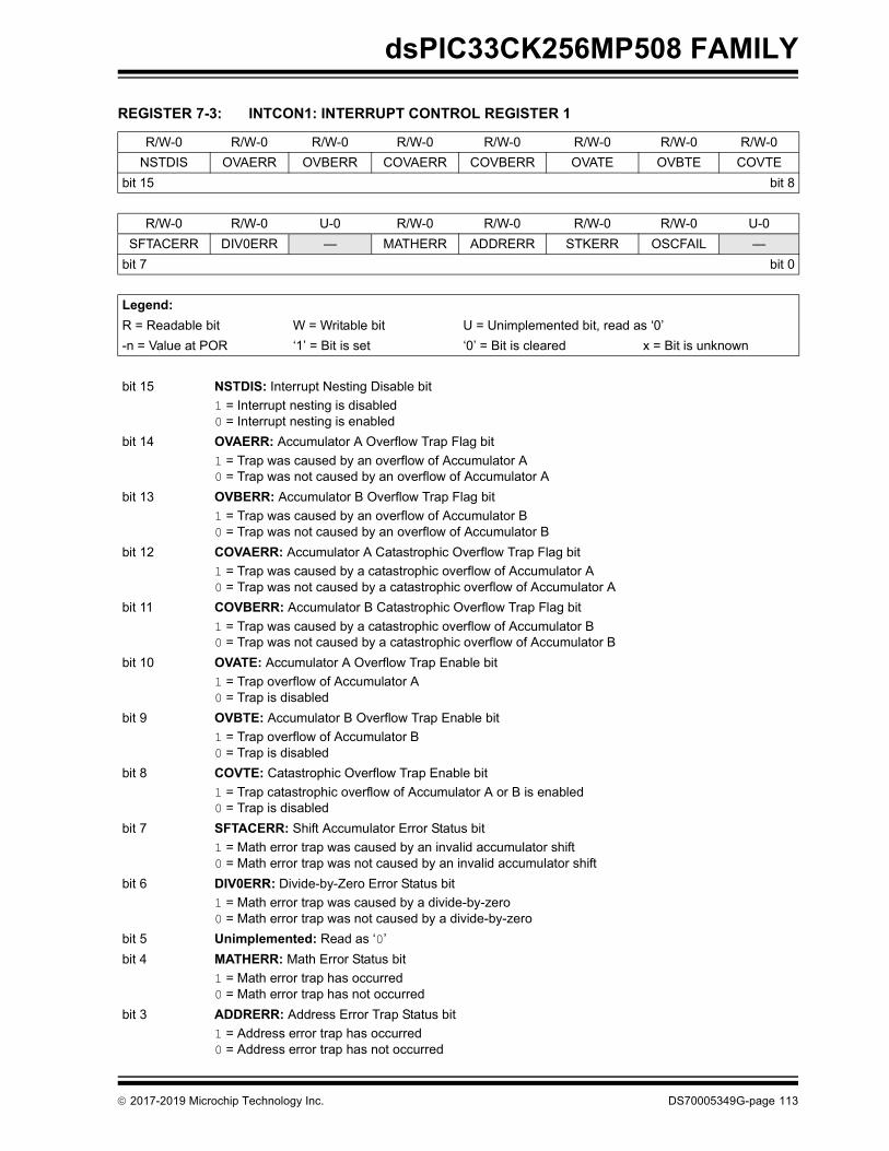
dsPIC33CK256MP508 FAMILY
REGISTER 7-3: INTCON1: INTERRUPT CONTROL REGISTER 1
R/W-0 R/W-0 R/W-0 R/W-0 R/W-0 R/W-0 R/W-0 R/W-0NSTDIS OVAERR OVBERR COVAERR COVBERR OVATE OVBTE COVTE
bit 15 bit 8
R/W-0 R/W-0 U-0 R/W-0 R/W-0 R/W-0 R/W-0 U-0SFTACERR DIV0ERR — MATHERR ADDRERR STKERR OSCFAIL —
bit 7 bit 0
Legend:R = Readable bit W = Writable bit U = Unimplemented bit, read as ‘0’-n = Value at POR ‘1’ = Bit is set ‘0’ = Bit is cleared x = Bit is unknown
bit 15 NSTDIS: Interrupt Nesting Disable bit1 = Interrupt nesting is disabled0 = Interrupt nesting is enabled
bit 14 OVAERR: Accumulator A Overflow Trap Flag bit1 = Trap was caused by an overflow of Accumulator A0 = Trap was not caused by an overflow of Accumulator A
bit 13 OVBERR: Accumulator B Overflow Trap Flag bit1 = Trap was caused by an overflow of Accumulator B0 = Trap was not caused by an overflow of Accumulator B
bit 12 COVAERR: Accumulator A Catastrophic Overflow Trap Flag bit1 = Trap was caused by a catastrophic overflow of Accumulator A0 = Trap was not caused by a catastrophic overflow of Accumulator A
bit 11 COVBERR: Accumulator B Catastrophic Overflow Trap Flag bit1 = Trap was caused by a catastrophic overflow of Accumulator B0 = Trap was not caused by a catastrophic overflow of Accumulator B
bit 10 OVATE: Accumulator A Overflow Trap Enable bit1 = Trap overflow of Accumulator A0 = Trap is disabled
bit 9 OVBTE: Accumulator B Overflow Trap Enable bit1 = Trap overflow of Accumulator B0 = Trap is disabled
bit 8 COVTE: Catastrophic Overflow Trap Enable bit1 = Trap catastrophic overflow of Accumulator A or B is enabled0 = Trap is disabled
bit 7 SFTACERR: Shift Accumulator Error Status bit1 = Math error trap was caused by an invalid accumulator shift0 = Math error trap was not caused by an invalid accumulator shift
bit 6 DIV0ERR: Divide-by-Zero Error Status bit1 = Math error trap was caused by a divide-by-zero0 = Math error trap was not caused by a divide-by-zero
bit 5 Unimplemented: Read as ‘0’bit 4 MATHERR: Math Error Status bit
1 = Math error trap has occurred0 = Math error trap has not occurred
bit 3 ADDRERR: Address Error Trap Status bit1 = Address error trap has occurred0 = Address error trap has not occurred
2017-2019 Microchip Technology Inc. DS70005349G-page 113

dsPIC33CK256MP508 FAMILY
bit 2 STKERR: Stack Error Trap Status bit1 = Stack error trap has occurred0 = Stack error trap has not occurred
bit 1 OSCFAIL: Oscillator Failure Trap Status bit1 = Oscillator failure trap has occurred0 = Oscillator failure trap has not occurred
bit 0 Unimplemented: Read as ‘0’
REGISTER 7-3: INTCON1: INTERRUPT CONTROL REGISTER 1 (CONTINUED)
DS70005349G-page 114 2017-2019 Microchip Technology Inc.

dsPIC33CK256MP508 FAMILY
REGISTER 7-4: INTCON2: INTERRUPT CONTROL REGISTER 2
R/W-1 R/W-0 R/W-0 U-0 U-0 U-0 U-0 R/W-0GIE DISI SWTRAP — — — — AIVTEN
bit 15 bit 8
U-0 U-0 U-0 U-0 R/W-0 R/W-0 R/W-0 R/W-0— — — — INT3EP INT2EP INT1EP INT0EP
bit 7 bit 0
Legend:R = Readable bit W = Writable bit U = Unimplemented bit, read as ‘0’-n = Value at POR ‘1’ = Bit is set ‘0’ = Bit is cleared x = Bit is unknown
bit 15 GIE: Global Interrupt Enable bit1 = Interrupts and associated IE bits are enabled 0 = Interrupts are disabled, but traps are still enabled
bit 14 DISI: DISI Instruction Status bit1 = DISI instruction is active0 = DISI instruction is not active
bit 13 SWTRAP: Software Trap Status bit1 = Software trap is enabled0 = Software trap is disabled
bit 12-9 Unimplemented: Read as ‘0’bit 8 AIVTEN: Alternate Interrupt Vector Table Enable bit
1 = Uses Alternate Interrupt Vector Table0 = Uses standard Interrupt Vector Table
bit 7-4 Unimplemented: Read as ‘0’bit 3 INT3EP: External Interrupt 3 Edge Detect Polarity Select bit
1 = Interrupt on negative edge 0 = Interrupt on positive edge
bit 2 INT2EP: External Interrupt 2 Edge Detect Polarity Select bit1 = Interrupt on negative edge 0 = Interrupt on positive edge
bit 1 INT1EP: External Interrupt 1 Edge Detect Polarity Select bit1 = Interrupt on negative edge 0 = Interrupt on positive edge
bit 0 INT0EP: External Interrupt 0 Edge Detect Polarity Select bit1 = Interrupt on negative edge 0 = Interrupt on positive edge
2017-2019 Microchip Technology Inc. DS70005349G-page 115

dsPIC33CK256MP508 FAMILY
REGISTER 7-5: INTCON3: INTERRUPT CONTROL REGISTER 3
U-0 U-0 U-0 U-0 U-0 U-0 R/W-0 R/W-0— — — — — — CAN(1) NAE
bit 15 bit 8
U-0 U-0 R/W-0 R/W-0 U-0 U-0 U-0 R/W-0— — DAE DOOVR — — — APLL
bit 7 bit 0
Legend:R = Readable bit W = Writable bit U = Unimplemented bit, read as ‘0’-n = Value at POR ‘1’ = Bit is set ‘0’ = Bit is cleared x = Bit is unknown
bit 15-10 Unimplemented: Read as ‘0’bit 9 CAN: CAN Address Error Soft Trap Status bit(1)
1 = CAN address error soft trap has occurred0 = CAN address error soft trap has not occurred
bit 8 NAE: NVM Address Error Soft Trap Status bit1 = NVM address error soft trap has occurred0 = NVM address error soft trap has not occurred
bit 7-6 Unimplemented: Read as ‘0’bit 5 DAE: DMA Address Error (Soft) Trap Status bit
1 = DMA address error trap has occurred0 = Trap has not occurred
bit 4 DOOVR: DO Stack Overflow Soft Trap Status bit1 = DO stack overflow soft trap has occurred0 = DO stack overflow soft trap has not occurred
bit 3-1 Unimplemented: Read as ‘0’bit 0 APLL: Auxiliary PLL Loss of Lock Soft Trap Status bit
1 = APLL lock soft trap has occurred0 = APLL lock soft trap has not occurred
Note 1: The CAN peripheral is not available on all devices. Refer to Table 1 and Table 2 for availability.
DS70005349G-page 116 2017-2019 Microchip Technology Inc.

dsPIC33CK256MP508 FAMILY
REGISTER 7-6: INTCON4: INTERRUPT CONTROL REGISTER 4
U-0 U-0 U-0 U-0 U-0 U-0 U-0 U-0— — — — — — — —
bit 15 bit 8
U-0 U-0 U-0 U-0 U-0 U-0 R/W-0 R/W-0— — — — — — ECCDBE SGHT
bit 7 bit 0
Legend:R = Readable bit W = Writable bit U = Unimplemented bit, read as ‘0’-n = Value at POR ‘1’ = Bit is set ‘0’ = Bit is cleared x = Bit is unknown
bit 15-2 Unimplemented: Read as ‘0’bit 1 ECCDBE: ECC Double-Bit Error Trap bit
1 = ECC double-bit error trap has occurred0 = ECC double-bit error trap has not occurred
bit 0 SGHT: Software Generated Hard Trap Status bit1 = Software generated hard trap has occurred0 = Software generated hard trap has not occurred
2017-2019 Microchip Technology Inc. DS70005349G-page 117

dsPIC33CK256MP508 FAMILY
REGISTER 7-7: INTTREG: INTERRUPT CONTROL AND STATUS REGISTER
U-0 U-0 R-0 U-0 R-0 R-0 R-0 R-0— — VHOLD — ILR3 ILR2 ILR1 ILR0
bit 15 bit 8
R-0 R-0 R-0 R-0 R-0 R-0 R-0 R-0VECNUM7 VECNUM6 VECNUM5 VECNUM4 VECNUM3 VECNUM2 VECNUM1 VECNUM0
bit 7 bit 0
Legend:R = Readable bit W = Writable bit U = Unimplemented bit, read as ‘0’-n = Value at POR ‘1’ = Bit is set ‘0’ = Bit is cleared x = Bit is unknown
bit 15-14 Unimplemented: Read as ‘0’bit 13 VHOLD: Vector Number Capture Enable bit
1 = VECNUM[7:0] bits read current value of vector number encoding tree (i.e., highest priority pendinginterrupt)
0 = Vector number latched into VECNUM[7:0] at Interrupt Acknowledge and retained until next IACKbit 12 Unimplemented: Read as ‘0’bit 11-8 ILR[3:0]: New CPU Interrupt Priority Level bits
1111 = CPU Interrupt Priority Level is 15...0001 = CPU Interrupt Priority Level is 10000 = CPU Interrupt Priority Level is 0
bit 7-0 VECNUM[7:0]: Vector Number of Pending Interrupt bits11111111 = 255, Reserved; do not use...00001001 = 9, IC1 – Input Capture 100001000 = 8, INT0 – External Interrupt 000000111 = 7, Reserved; do not use00000110 = 6, Generic soft trap00000101 = 5, Reserved; do not use00000100 = 4, Math error trap00000011 = 3, Stack error trap00000010 = 2, Generic hard trap00000001 = 1, Address error trap00000000 = 0, Oscillator fail trap
DS70005349G-page 118 2017-2019 Microchip Technology Inc.

dsPIC33CK256MP508 FAMILY
8.0 I/O PORTS
Many of the device pins are shared among the peripher-als and the Parallel I/O ports. All I/O input ports featureSchmitt Trigger inputs for improved noise immunity. ThePORT registers are located in the SFR.Some of the key features of the I/O ports are:• Individual Output Pin Open-Drain Enable/Disable• Individual Input Pin Weak Pull-up and Pull-Down• Monitor Selective Inputs and Generate Interrupt
when Change in Pin State is Detected• Operation during Sleep and Idle modes
8.1 Parallel I/O (PIO) PortsAll port pins have 12 registers directly associated withtheir operation as digital I/Os. The Data Directionregister (TRISx) determines whether the pin is an inputor an output. If the data direction bit is a ‘1’, then the pinis an input.All port pins are defined as inputs after a Reset. Readsfrom the latch (LATx), read the latch. Writes to the latch,write the latch. Reads from the port (PORTx), read theport pins, while writes to the port pins, write the latch. Anybit and its associated data and control registers that arenot valid for a particular device are disabled. This meansthe corresponding LATx and TRISx registers, and theport pin are read as zeros.When a pin is shared with another peripheral or func-tion that is defined as an input only, it is neverthelessregarded as a dedicated port because there is noother competing source of outputs. Table 8-1 showsthe pin availability. Table 8-2 shows the 5V inputtolerant pins across this device.
Note 1: This data sheet summarizes the featuresof the dsPIC33CK256MP508 family ofdevices. It is not intended to be a compre-hensive reference source. To complementthe information in this data sheet, referto “I/O Ports with Edge Detect”(www.microchip.com/DS70005322) in the“dsPIC33/PIC24 Family ReferenceManual”.
2: Some registers and associated bitsdescribed in this section may not beavailable on all devices.
2017-2019 Microchip Technology Inc. DS70005349G-page 119

dsPIC33CK256MP508 FAMILY
TABLE 8-1: PIN AND ANSELx AVAILABILITYDevice Rx15 Rx14 Rx13 Rx12 Rx11 Rx10 Rx9 Rx8 Rx7 Rx6 Rx5 Rx4 Rx3 Rx2 Rx1 Rx0
PORTAdsPIC33XXXMP508/208 — — — — — — — — — — — X X X X XdsPIC33XXXMP506/206 — — — — — — — — — — — X X X X XdsPIC33XXXMP504/204 — — — — — — — — — — — X X X X XdsPIC33XXXMP503/203 — — — — — — — — — — — X X X X XdsPIC33XXXMP502/202 — — — — — — — — — — — X X X X X
ANSELA — — — — — — — — — — — X X X X XPORTB
dsPIC33XXXMP508/208 X X X X X X X X X X X X X X X XdsPIC33XXXMP506/206 X X X X X X X X X X X X X X X XdsPIC33XXXMP504/204 X X X X X X X X X X X X X X X XdsPIC33XXXMP503/203 X X X X X X X X X X X X X X X XdsPIC33XXXMP502/202 X X X X X X X X X X X X X X X X
ANSELB — — — — — — X X X — — X X X X XPORTC
dsPIC33XXXMP508/208 X X X X X X X X X X X X X X X XdsPIC33XXXMP506/206 X X X X X X X X X X X X X X X XdsPIC33XXXMP504/204 — — X X X X X X X X X X X X X XdsPIC33XXXMP503/203 — — — — — — — — — — X X X X X XdsPIC33XXXMP502/202 — — — — — — — — — — — — — — — —
ANSELC — — — — — — — — X X — — X X X XPORTD
dsPIC33XXXMP508/208 X X X X X X X X X X X X X X X XdsPIC33XXXMP506/206 X X X X X X X X X X X X X X X XdsPIC33XXXMP504/204 — — X — — X — X — — — — — — X —dsPIC33XXXMP503/203 — — — — — — — — — — — — — — — —dsPIC33XXXMP502/202 — — — — — — — — — — — — — — — —
ANSELD — — X — X X — — — — — — — — — —PORTE
dsPIC33XXXMP508/208 X X X X X X X X X X X X X X X XdsPIC33XXXMP506/206 — — — — — — — — — — — — — — — —dsPIC33XXXMP504/204 — — — — — — — — — — — — — — — —dsPIC33XXXMP503/203 — — — — — — — — — — — — — — — —dsPIC33XXXMP502/202 — — — — — — — — — — — — — — — —
ANSELE — — — — — — — — — — — X X X X X
TABLE 8-2: 5V INPUT TOLERANT PORTSPORTA — — — — — — — — — — — RA4 RA3 RA2 RA1 RA0PORTB RB15 RB14 RB13 RB12 RB11 RB10 RB9 RB8 RB7 RB6 RB5 RB4 RB3 RB2 RB1 RB0PORTC RC15 RC14 RC13 RC12 RC11 RC10 RC9 RC8 RC7 RC6 RC5 RC4 RC3 RC2 RC1 RC0PORTD RD15 RD14 RD13 RD12 RD11 RD10 RD9 RD8 RD7 RD6 RD5 RD4 RD3 RD2 RD1 RD0PORTE RE15 RE14 RE13 RE12 RE11 RE10 RE9 RE8 RE7 RE6 RE5 RE4 RE3 RE2 RE1 RE0
Legend: Shaded pins are up to 5.5 VDC input tolerant.
DS70005349G-page 120 2017-2019 Microchip Technology Inc.

dsPIC33CK256MP508 FAMILY
FIGURE 8-1: BLOCK DIAGRAM OF A TYPICAL SHARED PORT STRUCTURE
QD
CK
WR LATx +
TRISx Latch
I/O Pin
WR PORTx
Data Bus
QD
CK
Data Latch
Read PORTx
Read TRISx
WR TRISx
Peripheral Output DataOutput Enable
Peripheral Input Data
I/O
Peripheral Module
Peripheral Output Enable
PIO Module
Output Multiplexers
Output Data
Input Data
Peripheral Module Enable
Read LATx
1
0
10
2017-2019 Microchip Technology Inc. DS70005349G-page 121

dsPIC33CK256MP508 FAMILY
8.1.1 OPEN-DRAIN CONFIGURATIONIn addition to the PORTx, LATx and TRISx registersfor data control, port pins can also be individuallyconfigured for either digital or open-drain output. Thisis controlled by the Open-Drain Enable for PORTxregister, ODCx, associated with each port. Setting anyof the bits configures the corresponding pin to act asan open-drain output. The open-drain feature allows the generation ofoutputs, other than VDD, by using external pull-up resis-tors. The maximum open-drain voltage allowed on anypin is the same as the maximum VIH specification forthat particular pin.
8.2 Configuring Analog and Digital Port Pins
The ANSELx registers control the operation of theanalog port pins. The port pins that are to function asanalog inputs or outputs must have their correspondingANSELx and TRISx bits set. In order to use port pins forI/O functionality with digital modules, such as timers,UARTs, etc., the corresponding ANSELx bit must becleared.The ANSELx registers have a default value of 0xFFFF;therefore, all pins that share analog functions areanalog (not digital) by default.Pins with analog functions affected by the ANSELxregisters are listed with a buffer type of analog in thePinout I/O Descriptions (see Table 1-1).If the TRISx bit is cleared (output) while the ANSELx bitis set, the digital output level (VOH or VOL) is convertedby an analog peripheral, such as the ADC module orcomparator module.
When the PORTx register is read, all pins configured asanalog input channels are read as cleared (a low level).Pins configured as digital inputs do not convert ananalog input. Analog levels on any pin, defined as adigital input (including the ANx pins), can cause theinput buffer to consume current that exceeds thedevice specifications.
8.2.1 I/O PORT WRITE/READ TIMINGOne instruction cycle is required between a portdirection change or port write operation and a readoperation of the same port. Typically, this instructionwould be a NOP.
8.3 PORT Control RegistersThe following registers are in the PORT module:• Register 8-1: ANSELx (one per port) • Register 8-2: TRISx (one per port)• Register 8-3: PORTx (one per port)• Register 8-4: LATx (one per port)• Register 8-5: ODCx (one per port)• Register 8-6: CNPUx (one per port)• Register 8-7: CNPDx (one per port)• Register 8-8: CNCONx (one per port – optional)• Register 8-9: CNEN0x (one per port)• Register 8-10: CNSTATx (one per port – optional)• Register 8-11: CNEN1x (one per port)• Register 8-12: CNFx (one per port)
REGISTER 8-1: ANSELx: ANALOG SELECT FOR PORTx REGISTER
R/W-1 R/W-1 R/W-1 R/W-1 R/W-1 R/W-1 R/W-1 R/W-1ANSELx[15:8]
bit 15 bit 8
R/W-1 R/W-1 R/W-1 R/W-1 R/W-1 R/W-1 R/W-1 R/W-1ANSELx[7:0]
bit 7 bit 0
Legend:R = Readable bit W = Writable bit U = Unimplemented bit, read as ‘0’-n = Value at POR ‘1’ = Bit is set ‘0’ = Bit is cleared x = Bit is unknown
bit 15-0 ANSELx[15:0]: Analog Select for PORTx bits1 = Analog input is enabled and digital input is disabled on the PORTx[n] pin0 = Analog input is disabled and digital input is enabled on the PORTx[n] pin
DS70005349G-page 122 2017-2019 Microchip Technology Inc.

dsPIC33CK256MP508 FAMILY
REGISTER 8-2: TRISx: OUTPUT ENABLE FOR PORTx REGISTER
R/W-1 R/W-1 R/W-1 R/W-1 R/W-1 R/W-1 R/W-1 R/W-1TRISx[15:8]
bit 15 bit 8
R/W-1 R/W-1 R/W-1 R/W-1 R/W-1 R/W-1 R/W-1 R/W-1TRISx[7:0]
bit 7 bit 0
Legend:R = Readable bit W = Writable bit U = Unimplemented bit, read as ‘0’-n = Value at POR ‘1’ = Bit is set ‘0’ = Bit is cleared x = Bit is unknown
bit 15-0 TRISx[15:0]: Output Enable for PORTx bits1 = LATx[n] is not driven on the PORTx[n] pin0 = LATx[n] is driven on the PORTx[n] pin
REGISTER 8-3: PORTx: INPUT DATA FOR PORTx REGISTER
R/W-1 R/W-1 R/W-1 R/W-1 R/W-1 R/W-1 R/W-1 R/W-1PORTx[15:8]
bit 15 bit 8
R/W-1 R/W-1 R/W-1 R/W-1 R/W-1 R/W-1 R/W-1 R/W-1PORTx[7:0]
bit 7 bit 0
Legend:R = Readable bit W = Writable bit U = Unimplemented bit, read as ‘0’-n = Value at POR ‘1’ = Bit is set ‘0’ = Bit is cleared x = Bit is unknown
bit 15-0 PORTx[15:0]: PORTx Data Input Value bits
2017-2019 Microchip Technology Inc. DS70005349G-page 123

dsPIC33CK256MP508 FAMILY
REGISTER 8-4: LATx: OUTPUT DATA FOR PORTx REGISTER
R/W-x R/W-x R/W-x R/W-x R/W-x R/W-x R/W-x R/W-xLATx[15:8]
bit 15 bit 8
R/W-x R/W-x R/W-x R/W-x R/W-x R/W-x R/W-x R/W-xLATx[7:0]
bit 7 bit 0
Legend:R = Readable bit W = Writable bit U = Unimplemented bit, read as ‘0’-n = Value at POR ‘1’ = Bit is set ‘0’ = Bit is cleared x = Bit is unknown
bit 15-0 LATx[15:0]: PORTx Data Output Value bits
REGISTER 8-5: ODCx: OPEN-DRAIN ENABLE FOR PORTx REGISTER
R/W-0 R/W-0 R/W-0 R/W-0 R/W-0 R/W-0 R/W-0 R/W-0ODCx[15:8]
bit 15 bit 8
R/W-0 R/W-0 R/W-0 R/W-0 R/W-0 R/W-0 R/W-0 R/W-0ODCx[7:0]
bit 7 bit 0
Legend:R = Readable bit W = Writable bit U = Unimplemented bit, read as ‘0’-n = Value at POR ‘1’ = Bit is set ‘0’ = Bit is cleared x = Bit is unknown
bit 15-0 ODCx[15:0]: PORTx Open-Drain Enable bits1 = Open-drain is enabled on the PORTx pin0 = Open-drain is disabled on the PORTx pin
DS70005349G-page 124 2017-2019 Microchip Technology Inc.

dsPIC33CK256MP508 FAMILY
REGISTER 8-6: CNPUx: CHANGE NOTIFICATION PULL-UP ENABLE FOR PORTx REGISTER
R/W-0 R/W-0 R/W-0 R/W-0 R/W-0 R/W-0 R/W-0 R/W-0CNPUx[15:8]
bit 15 bit 8
R/W-0 R/W-0 R/W-0 R/W-0 R/W-0 R/W-0 R/W-0 R/W-0CNPUx[7:0]
bit 7 bit 0
Legend:R = Readable bit W = Writable bit U = Unimplemented bit, read as ‘0’-n = Value at POR ‘1’ = Bit is set ‘0’ = Bit is cleared x = Bit is unknown
bit 15-0 CNPUx[15:0]: Change Notification Pull-up Enable for PORTx bits1 = The pull-up for PORTx[n] is enabled – takes precedence over the pull-down selection0 = The pull-up for PORTx[n] is disabled
REGISTER 8-7: CNPDx: CHANGE NOTIFICATION PULL-DOWN ENABLE FOR PORTx REGISTER
R/W-0 R/W-0 R/W-0 R/W-0 R/W-0 R/W-0 R/W-0 R/W-0CNPDx[15:8]
bit 15 bit 8
R/W-0 R/W-0 R/W-0 R/W-0 R/W-0 R/W-0 R/W-0 R/W-0CNPDx[7:0]
bit 7 bit 0
Legend:R = Readable bit W = Writable bit U = Unimplemented bit, read as ‘0’-n = Value at POR ‘1’ = Bit is set ‘0’ = Bit is cleared x = Bit is unknown
bit 15-0 CNPDx[15:0]: Change Notification Pull-Down Enable for PORTx bits1 = The pull-down for PORTx[n] is enabled (if the pull-up for PORTx[n] is not enabled)0 = The pull-down for PORTx[n] is disabled
2017-2019 Microchip Technology Inc. DS70005349G-page 125

dsPIC33CK256MP508 FAMILY
REGISTER 8-8: CNCONx: CHANGE NOTIFICATION CONTROL FOR PORTx REGISTER
R/W-0 U-0 U-0 U-0 R/W-0 U-0 U-0 U-0ON — — — CNSTYLE — — —
bit 15 bit 8
U-0 U-0 U-0 U-0 U-0 U-0 U-0 U-0— — — — — — — —
bit 7 bit 0
Legend:R = Readable bit W = Writable bit U = Unimplemented bit, read as ‘0’-n = Value at POR ‘1’ = Bit is set ‘0’ = Bit is cleared x = Bit is unknown
bit 15 ON: Change Notification (CN) Control for PORTx On bit1 = CN is enabled0 = CN is disabled
bit 14-12 Unimplemented: Read as ‘0’bit 11 CNSTYLE: Change Notification Style Selection bit
1 = Edge style (detects edge transitions, CNFx[15:0] bits are used for a Change Notification event) 0 = Mismatch style (detects change from last port read, CNSTATx[15:0] bits are used for a Change
Notification event) bit 10-0 Unimplemented: Read as ‘0’
REGISTER 8-9: CNEN0x: CHANGE NOTIFICATION INTERRUPT ENABLE FOR PORTx REGISTER
R/W-0 R/W-0 R/W-0 R/W-0 R/W-0 R/W-0 R/W-0 R/W-0CNEN0x[15:8]
bit 15 bit 8
R/W-0 R/W-0 R/W-0 R/W-0 R/W-0 R/W-0 R/W-0 R/W-0CNEN0x[7:0]
bit 7 bit 0
Legend:R = Readable bit W = Writable bit U = Unimplemented bit, read as ‘0’-n = Value at POR ‘1’ = Bit is set ‘0’ = Bit is cleared x = Bit is unknown
bit 15-0 CNEN0x[15:0]: Change Notification Interrupt Enable for PORTx bits1 = Interrupt-on-change (from the last read value) is enabled for PORTx[n]0 = Interrupt-on-change is disabled for PORTx[n]
DS70005349G-page 126 2017-2019 Microchip Technology Inc.

dsPIC33CK256MP508 FAMILY
REGISTER 8-10: CNSTATx: CHANGE NOTIFICATION STATUS FOR PORTx REGISTER
R-0 R-0 R-0 R-0 R-0 R-0 R-0 R-0CNSTATx[15:8]
bit 15 bit 8
R-0 R-0 R-0 R-0 R-0 R-0 R-0 R-0CNSTATx[7:0]
bit 7 bit 0
Legend:R = Readable bit W = Writable bit U = Unimplemented bit, read as ‘0’-n = Value at POR ‘1’ = Bit is set ‘0’ = Bit is cleared x = Bit is unknown
bit 15-0 CNSTATx[15:0]: Change Notification Status for PORTx bitsWhen CNSTYLE (CNCONx[11]) = 0:1 = Change occurred on PORTx[n] since last read of PORTx[n]0 = Change did not occur on PORTx[n] since last read of PORTx[n]
REGISTER 8-11: CNEN1x: CHANGE NOTIFICATION EDGE SELECT FOR PORTx REGISTER
R/W-0 R/W-0 R/W-0 R/W-0 R/W-0 R/W-0 R/W-0 R/W-0CNEN1x[15:8]
bit 15 bit 8
R/W-0 R/W-0 R/W-0 R/W-0 R/W-0 R/W-0 R/W-0 R/W-0CNEN1x[7:0]
bit 7 bit 0
Legend:R = Readable bit W = Writable bit U = Unimplemented bit, read as ‘0’-n = Value at POR ‘1’ = Bit is set ‘0’ = Bit is cleared x = Bit is unknown
bit 15-0 CNEN1x[15:0]: Change Notification Edge Select for PORTx bits
2017-2019 Microchip Technology Inc. DS70005349G-page 127

dsPIC33CK256MP508 FAMILY
REGISTER 8-12: CNFx: CHANGE NOTIFICATION INTERRUPT FLAG FOR PORTx REGISTER
R/W-0 R/W-0 R/W-0 R/W-0 R/W-0 R/W-0 R/W-0 R/W-0CNFx[15:8]
bit 15 bit 8
R/W-0 R/W-0 R/W-0 R/W-0 R/W-0 R/W-0 R/W-0 R/W-0CNFx[7:0]
bit 7 bit 0
Legend:R = Readable bit W = Writable bit U = Unimplemented bit, read as ‘0’-n = Value at POR ‘1’ = Bit is set ‘0’ = Bit is cleared x = Bit is unknown
bit 15-0 CNFx[15:0]: Change Notification Interrupt Flag for PORTx bitsWhen CNSTYLE (CNCONx[11]) = 1:1 = An enabled edge event occurred on the PORTx[n] pin0 = An enabled edge event did not occur on the PORTx[n] pin
DS70005349G-page 128 2017-2019 Microchip Technology Inc.

dsPIC33CK256MP508 FAMILY
8.4 Input Change Notification (ICN)The Input Change Notification function of the I/O portsallows the dsPIC33CK256MP508 family devices to gen-erate interrupt requests to the processor in response toa Change-of-State (COS) on selected input pins. Thisfeature can detect input Change-of-States, even inSleep mode, when the clocks are disabled. Every I/Oport pin can be selected (enabled) for generating aninterrupt request on a Change-of-State. Five controlregisters are associated with the Change Notification(CN) functionality of each I/O port. To enable theChange Notification feature for the port, the ON bit(CNCONx[15]) must be set.The CNEN0x and CNEN1x registers contain the CNinterrupt enable control bits for each of the input pins.The setting of these bits enables a CN interrupt for thecorresponding pins. Also, these bits, in combinationwith the CNSTYLE bit (CNCONx[11]), define a type oftransition when the interrupt is generated. Possible CNevent options are listed in Table 8-3.
The CNSTATx register indicates whether a changeoccurred on the corresponding pin since the last readof the PORTx bit. In addition to the CNSTATx register,the CNFx register is implemented for each port. Thisregister contains flags for Change Notification events.These flags are set if the valid transition edge, selectedin the CNEN0x and CNEN1x registers, is detected.CNFx stores the occurrence of the event. CNFx bitsmust be cleared in software to get the next ChangeNotification interrupt. The CN interrupt is generatedonly for the I/Os configured as inputs (correspondingTRISx bits must be set).
8.5 Peripheral Pin Select (PPS)A major challenge in general purpose devices isproviding the largest possible set of peripheral features,while minimizing the conflict of features on I/O pins.The challenge is even greater on low pin count devices.In an application where more than one peripheralneeds to be assigned to a single pin, inconvenientwork arounds in application code, or a completeredesign, may be the only option.Peripheral Pin Select configuration provides an alter-native to these choices by enabling peripheral setselection and placement on a wide range of I/O pins.By increasing the pinout options available on a particu-lar device, users can better tailor the device to theirentire application, rather than trimming the applicationto fit the device.The Peripheral Pin Select configuration featureoperates over a fixed subset of digital I/O pins. Usersmay independently map the input and/or output of mostdigital peripherals to any one of these I/O pins. Hard-ware safeguards are included that prevent accidentalor spurious changes to the peripheral mapping once ithas been established.
8.5.1 AVAILABLE PINSThe number of available pins is dependent on the par-ticular device and its pin count. Pins that support thePeripheral Pin Select feature include the label, “RPn”,in their full pin designation, where “n” is the remappablepin number. “RP” is used to designate pins that supportboth remappable input and output functions.
8.5.2 AVAILABLE PERIPHERALSThe peripherals managed by the Peripheral Pin Selectare all digital only peripherals. These include generalserial communications (UART and SPI), general pur-pose timer clock inputs, timer-related peripherals (inputcapture and output compare) and interrupt-on-changeinputs.In comparison, some digital only peripheral modulesare never included in the Peripheral Pin Select feature.This is because the peripheral’s function requiresspecial I/O circuitry on a specific port and cannot beeasily connected to multiple pins. One exampleincludes I2C modules. A similar requirement excludesall modules with analog inputs, such as the A/DConverter (ADC)A key difference between remappable and non-remappable peripherals is that remappable peripheralsare not associated with a default I/O pin. The peripheralmust always be assigned to a specific I/O pin before itcan be used. In contrast, non-remappable peripheralsare always available on a default pin, assuming that theperipheral is active and not conflicting with anotherperipheral.
TABLE 8-3: CHANGE NOTIFICATION EVENT OPTIONS
CNSTYLE Bit (CNCONx[11])
CNEN1x Bit
CNEN0x Bit
Change Notification Event Description
0 Does not matter
0 Disabled
0 Does not matter
1 Detects a mismatch between the last read state and the current state of the pin
1 0 0 Disabled
1 0 1 Detects a positive transition only (from ‘0’ to ‘1’)
1 1 0 Detects a negative transition only (from ‘1’ to ‘0’)
1 1 1 Detects both positive and negative transitions
Note: Pull-ups and pull-downs on Input ChangeNotification pins should always bedisabled when the port pin is configuredas a digital output.
2017-2019 Microchip Technology Inc. DS70005349G-page 129

dsPIC33CK256MP508 FAMILY
When a remappable peripheral is active on a given I/Opin, it takes priority over all other digital I/Os and digitalcommunication peripherals associated with the pin.Priority is given regardless of the type of peripheral thatis mapped. Remappable peripherals never take priorityover any analog functions associated with the pin.
8.5.3 CONTROLLING CONFIGURATION CHANGES
Because peripheral mapping can be changed during runtime, some restrictions on peripheral remapping areneeded to prevent accidental configuration changes. ThedsPIC33CK256MP508 devices have implemented thecontrol register lock sequence.
8.5.3.1 Control Register LockUnder normal operation, writes to the RPINRx andRPORx registers are not allowed. Attempted writes willappear to execute normally, but the contents of theregisters will remain unchanged. To change these reg-isters, they must be unlocked in hardware. The registerlock is controlled by the IOLOCK bit (RPCON[11]).Setting IOLOCK prevents writes to the control registers;clearing IOLOCK allows writes. To set or clear IOLOCK,the NVMKEY unlock sequence must be executed:1. Write 0x55 to NVMKEY.2. Write 0xAA to NVMKEY.3. Clear (or set) IOLOCK as a single operation.IOLOCK remains in one state until changed. Thisallows all of the Peripheral Pin Selects to be configuredwith a single unlock sequence, followed by an updateto all of the control registers. Then, IOLOCK can be setwith a second lock sequence.
8.5.4 CONSIDERATIONS FOR PERIPHERAL PIN SELECTION
The ability to control Peripheral Pin Selection intro-duces several considerations into application designthat most users would never think of otherwise. This isparticularly true for several common peripherals, whichare only available as remappable peripherals.The main consideration is that the Peripheral PinSelects are not available on default pins in the device’sdefault (Reset) state. More specifically, because allRPINRx registers reset to ‘1’s and RPORx registersreset to ‘0’s, this means all PPS inputs are tied to VSS,while all PPS outputs are disconnected. This meansthat before any other application code is executed, theuser must initialize the device with the proper periph-eral configuration. Because the IOLOCK bit resets inthe unlocked state, it is not necessary to execute theunlock sequence after the device has come out ofReset. For application safety, however, it is alwaysbetter to set IOLOCK and lock the configuration afterwriting to the control registers.
The NVMKEY unlock sequence must be executed as anAssembly language routine. If the bulk of the applicationis written in C, or another high-level language, the unlocksequence should be performed by writing in-line assem-bly or by using the __builtin_write_RPCON(value)function provided by the compiler.Choosing the configuration requires a review of allPeripheral Pin Selects and their pin assignments, par-ticularly those that will not be used in the application. Inall cases, unused pin-selectable peripherals should bedisabled completely. Unused peripherals should havetheir inputs assigned to an unused RPn pin function.I/O pins with unused RPn functions should be configuredwith the null peripheral output.
8.5.5 INPUT MAPPINGThe inputs of the Peripheral Pin Select options aremapped on the basis of the peripheral. That is, a controlregister associated with a peripheral dictates the pin itwill be mapped to. The RPINRx registers are used toconfigure peripheral input mapping. Each register con-tains sets of 8-bit fields, with each set associated withone of the remappable peripherals. Programming agiven peripheral’s bit field with an appropriate 8-bitindex value maps the RPn pin with the correspondingvalue, or internal signal, to that peripheral. See Table 8-4for a list of available inputs.For example, Figure 8-2 illustrates remappable pinselection for the U1RX input. Example 8-1 provides aconfiguration for bidirectional communication with flowcontrol using UART1. The following input and outputfunctions are used:• Input Functions: U1RX, U1CTS• Output Functions: U1TX, U1RTS
Note: MPLAB® XC16 provides a built-in Clanguage function for unlocking andmodifying the RPCON register:__builtin_write_RPCON(value);For more information, see the “MPLAB®
XC16 C Compiler User’s Guide”(DS50002071).
DS70005349G-page 130 2017-2019 Microchip Technology Inc.

dsPIC33CK256MP508 FAMILY
EXAMPLE 8-1: CONFIGURING UART1 INPUT AND OUTPUT FUNCTIONS
FIGURE 8-2: REMAPPABLE INPUT FOR U1RX
//*******************************************// Unlock Registers//*****************************************__builtin_write_RPCON(0x0000);//*****************************************// Configure Input Functions (See Table 8-5)// Assign U1Rx To Pin RP35//***************************_U1RXR = 35;// Assign U1CTS To Pin RP36//***************************_U1CTSR = 36;//*****************************************// Configure Output Functions (See Table 8-7)//*****************************************// Assign U1Tx To Pin RP37//***************************_RP37 = 1;//***************************// Assign U1RTS To Pin RP38//***************************_RP38 = 2;//*****************************************// Lock Registers//*****************************************__builtin_write_RPCON(0x0800);
VSS
CMP1
RP32
0
1
32U1RX Input
U1RXR[7:0]
to Peripheral
RP181n
Note: For input only, Peripheral Pin Select functionality does not have priority over TRISx settings. Therefore, when configuring an RPn pin for input, the corresponding bit in the TRISx register must also be configured for input (set to ‘1’).Physical connection to a pin can be made through RP32 through RP71. There are internal signals and virtual pins that can be connected to an input. Table 8-4 shows the details of the input assignment.
2017-2019 Microchip Technology Inc. DS70005349G-page 131

dsPIC33CK256MP508 FAMILY
TABLE 8-4: REMAPPABLE PIN INPUTS RPINRx[15:8] or
RPINRx[7:0] Function Available on Ports
0 VSS Internal1 Comparator 1 Internal 2 Comparator 2 Internal 3 Comparator 3 Internal
4-5 RP4-RP5 Reserved6 PTG Trigger 26 Internal 7 PTG Trigger 27 Internal
8-10 RP8-RP10 Reserved11 PWM Event Out C Internal 12 PWM Event Out D Internal 13 PWM Event Out E Internal
14-31 RP14-RP31 Reserved32 RP32 Port Pin RB033 RP33 Port Pin RB134 RP34 Port Pin RB235 RP35 Port Pin RB336 RP36 Port Pin RB437 RP37 Port Pin RB538 RP38 Port Pin RB639 RP39 Port Pin RB740 RP40 Port Pin RB841 RP41 Port Pin RB942 RP42 Port Pin RB1043 RP43 Port Pin RB1144 RP44 Port Pin RB1245 RP45 Port Pin RB1346 RP46 Port Pin RB1447 RP47 Port Pin RB1548 RP48 Port Pin RC049 RP49 Port Pin RC150 RP50 Port Pin RC251 RP51 Port Pin RC352 RP52 Port Pin RC453 RP53 Port Pin RC554 RP54 Port Pin RC655 RP55 Port Pin RC756 RP56 Port Pin RC857 RP57 Port Pin RC958 RP58 Port Pin RC1059 RP59 Port Pin RC1160 RP60 Port Pin RC1261 RP61 Port Pin RC1362 RP62 Port Pin RC14
DS70005349G-page 132 2017-2019 Microchip Technology Inc.

dsPIC33CK256MP508 FAMILY
8.5.6 VIRTUAL CONNECTIONSThe dsPIC33CK256MP508 devices support six virtualRPn pins (RP176-RP181), which are identical infunctionality to all other RPn pins, with the exception ofpinouts. These six pins are internal to the devices andare not connected to a physical device pin.
These pins provide a simple way for inter-peripheralconnection without utilizing a physical pin. Forexample, the output of the analog comparator can beconnected to RP176 and the PWM Fault input can beconfigured for RP176 as well. This configuration allowsthe analog comparator to trigger PWM Faults withoutthe use of an actual physical pin on the device.
63 RP63 Port Pin RC1564 RP64 Port Pin RD065 RP65 Port Pin RD166 RP66 Port Pin RD267 RP67 Port Pin RD368 RP68 Port Pin RD469 RP69 Port Pin RD570 RP70 Port Pin RD671 RP71 Port Pin RD772 RP72 Port Pin RD873 RP73 Port Pin RD974 RP74 Port Pin RD1075 RP75 Port Pin RD1176 RP76 Port Pin RD1277 RP77 Port Pin RD1378 RP78 Port Pin RD1479 RP79 Port Pin RD15
80-163 RP80-RP163 Reserved164 pwm_req_on[3] Internal165 pwm_req_off[3] Internal166 pwm_req_on[2] Internal167 pwm_req_off[2] Internal168 pwm_req_on[1] Internal169 pwm_req_off[1] Internal
170-175 RP170-RP175 Reserved176 RP176 Virtual RPV0177 RP177 Virtual RPV1178 RP178 Virtual RPV2179 RP179 Virtual RPV3180 RP180 Virtual RPV4181 RP181 Virtual RPV5
TABLE 8-4: REMAPPABLE PIN INPUTS (CONTINUED) RPINRx[15:8] or
RPINRx[7:0] Function Available on Ports
2017-2019 Microchip Technology Inc. DS70005349G-page 133
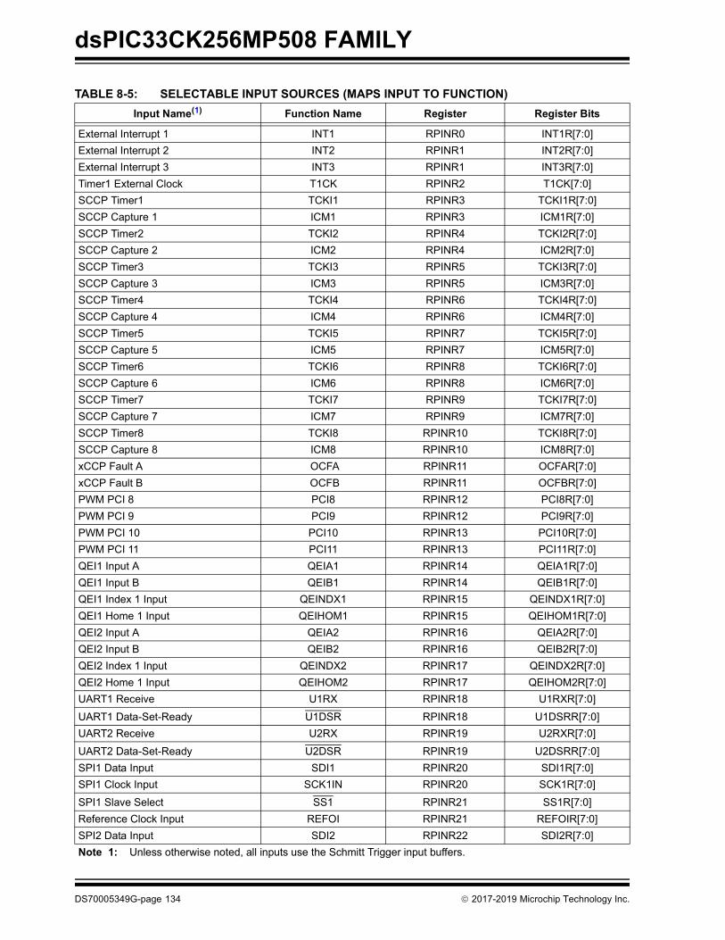
dsPIC33CK256MP508 FAMILY
TABLE 8-5: SELECTABLE INPUT SOURCES (MAPS INPUT TO FUNCTION)Input Name(1) Function Name Register Register Bits
External Interrupt 1 INT1 RPINR0 INT1R[7:0]External Interrupt 2 INT2 RPINR1 INT2R[7:0]External Interrupt 3 INT3 RPINR1 INT3R[7:0]Timer1 External Clock T1CK RPINR2 T1CK[7:0]SCCP Timer1 TCKI1 RPINR3 TCKI1R[7:0]SCCP Capture 1 ICM1 RPINR3 ICM1R[7:0]SCCP Timer2 TCKI2 RPINR4 TCKI2R[7:0]SCCP Capture 2 ICM2 RPINR4 ICM2R[7:0]SCCP Timer3 TCKI3 RPINR5 TCKI3R[7:0]SCCP Capture 3 ICM3 RPINR5 ICM3R[7:0]SCCP Timer4 TCKI4 RPINR6 TCKI4R[7:0]SCCP Capture 4 ICM4 RPINR6 ICM4R[7:0]SCCP Timer5 TCKI5 RPINR7 TCKI5R[7:0]SCCP Capture 5 ICM5 RPINR7 ICM5R[7:0]SCCP Timer6 TCKI6 RPINR8 TCKI6R[7:0]SCCP Capture 6 ICM6 RPINR8 ICM6R[7:0]SCCP Timer7 TCKI7 RPINR9 TCKI7R[7:0]SCCP Capture 7 ICM7 RPINR9 ICM7R[7:0]SCCP Timer8 TCKI8 RPINR10 TCKI8R[7:0]SCCP Capture 8 ICM8 RPINR10 ICM8R[7:0]xCCP Fault A OCFA RPINR11 OCFAR[7:0]xCCP Fault B OCFB RPINR11 OCFBR[7:0]PWM PCI 8 PCI8 RPINR12 PCI8R[7:0]PWM PCI 9 PCI9 RPINR12 PCI9R[7:0]PWM PCI 10 PCI10 RPINR13 PCI10R[7:0]PWM PCI 11 PCI11 RPINR13 PCI11R[7:0]QEI1 Input A QEIA1 RPINR14 QEIA1R[7:0]QEI1 Input B QEIB1 RPINR14 QEIB1R[7:0]QEI1 Index 1 Input QEINDX1 RPINR15 QEINDX1R[7:0]QEI1 Home 1 Input QEIHOM1 RPINR15 QEIHOM1R[7:0]QEI2 Input A QEIA2 RPINR16 QEIA2R[7:0]QEI2 Input B QEIB2 RPINR16 QEIB2R[7:0]QEI2 Index 1 Input QEINDX2 RPINR17 QEINDX2R[7:0]QEI2 Home 1 Input QEIHOM2 RPINR17 QEIHOM2R[7:0]UART1 Receive U1RX RPINR18 U1RXR[7:0]UART1 Data-Set-Ready U1DSR RPINR18 U1DSRR[7:0]UART2 Receive U2RX RPINR19 U2RXR[7:0]UART2 Data-Set-Ready U2DSR RPINR19 U2DSRR[7:0]SPI1 Data Input SDI1 RPINR20 SDI1R[7:0]SPI1 Clock Input SCK1IN RPINR20 SCK1R[7:0]SPI1 Slave Select SS1 RPINR21 SS1R[7:0]Reference Clock Input REFOI RPINR21 REFOIR[7:0]SPI2 Data Input SDI2 RPINR22 SDI2R[7:0]Note 1: Unless otherwise noted, all inputs use the Schmitt Trigger input buffers.
DS70005349G-page 134 2017-2019 Microchip Technology Inc.

dsPIC33CK256MP508 FAMILY
SPI2 Clock Input SCK2IN RPINR22 SCK2R[7:0]SPI2 Slave Select SS2 RPINR23 SS2R[7:0]CAN1 Input CAN1RX RPINR26 CAN1RXR[7:0]UART3 Receive U3RX RPINR27 U3RXR[7:0]UART3 Data-Set-Ready U3DSR RPINR27 U3DSRR[7:0]SPI3 Data Input SDI3 RPINR29 SDI3R[7:0]SPI3 Clock Input SCK3IN RPINR29 SCK3R[7:0]SPI3 Slave Select SS3 RPINR30 SS3R[7:0]MCCP Timer9 TCKI9 RPINR32 TCKI9R[7:0]MCCP Capture 9 ICM9 RPINR33 ICM9R[7:0]xCCP Fault C OCFC RPINR37 OCFCR[7:0]PWM Input 17 PCI17 RPINR37 PCI17R[7:0]PWM Input 18 PCI18 RPINR38 PCI18R[7:0]PWM Input 12 PCI12 RPINR42 PCI12R[7:0]PWM Input 13 PCI13 RPINR42 PCI13R[7:0]PWM Input 14 PCI14 RPINR43 PCI14R[7:0]PWM Input 15 PCI15 RPINR43 PCI15R[7:0]PWM Input 16 PCI16 RPINR44 PCI16R[7:0]SENT1 Input SENT1 RPINR44 SENT1R[7:0]SENT2 Input SENT2 RPINR45 SENT2R[7:0]CLC Input A CLCINA RPINR45 CLCINAR[7:0]CLC Input B CLCINB RPINR46 CLCINBR[7:0]CLC Input C CLCINC RPINR46 CLCINCR[7:0]CLC Input D CLCIND RPINR47 CLCINDR[7:0]ADC Trigger Input (ADTRIG31) ADCTRG RPINR47 ADCTRGR[7:0]xCCP Fault D OCFD RPINR48 OCFDR[7:0]UART1 Clear-to-Send U1CTS RPINR48 U1CTSR[7:0]UART2 Clear-to-Send U2CTS RPINR49 U2CTSR[7:0]UART3 Clear-to-Send U3CTS RPINR49 U3CTSR[7:0]
TABLE 8-5: SELECTABLE INPUT SOURCES (MAPS INPUT TO FUNCTION) (CONTINUED)Input Name(1) Function Name Register Register Bits
Note 1: Unless otherwise noted, all inputs use the Schmitt Trigger input buffers.
2017-2019 Microchip Technology Inc. DS70005349G-page 135

dsPIC33CK256MP508 FAMILY
8.5.7 OUTPUT MAPPINGIn contrast to inputs, the outputs of the Peripheral PinSelect options are mapped on the basis of the pin. Inthis case, a control register associated with a particularpin dictates the peripheral output to be mapped. TheRPORx registers are used to control output mapping.Each register contains sets of 6-bit fields, with each setassociated with one RPn pin (see Register 8-54through Register 8-80). The value of the bit field corre-sponds to one of the peripherals and that peripheral’soutput is mapped to the pin (see Table 8-7 andFigure 8-3).A null output is associated with the output registerReset value of ‘0’. This is done to ensure that remap-pable outputs remain disconnected from all output pinsby default.
FIGURE 8-3: MULTIPLEXING REMAPPABLE OUTPUTS FOR RPn
8.5.8 MAPPING LIMITATIONSThe control schema of the peripheral select pins is notlimited to a small range of fixed peripheral configura-tions. There are no mutual or hardware-enforcedlockouts between any of the peripheral mapping SFRs.Literally, any combination of peripheral mappings,across any or all of the RPn pins, is possible. Thisincludes both many-to-one and one-to-many mappingsof peripheral inputs, and outputs to pins. While suchmappings may be technically possible from a configu-ration point of view, they may not be supportable froman electrical point of view (see Table 8-6).
Note 1: There are six virtual output ports whichare not connected to any I/O ports(RP176-RP181). These virtual ports canbe accessed by RPOR20, RPOR21 andRPOR22.
RPnR[5:0]
0
54
1
Default
U1TX Output
SDO2 Output 2
PWM4L Output53PWM4H Output
Output Data
RP170-RP181(Internal Virtual
RP32-RP71(Physical Pins)
Output Ports)
DS70005349G-page 136 2017-2019 Microchip Technology Inc.

dsPIC33CK256MP508 FAMILY
TABLE 8-6: REMAPPABLE OUTPUT PIN REGISTERSRegister RP Pin I/O Port
RPOR0[5:0] RP32 Port Pin RB0RPOR0[13:8] RP33 Port Pin RB1RPOR1[5:0] RP34 Port Pin RB2RPOR1[13:8] RP35 Port Pin RB3RPOR2[5:0] RP36 Port Pin RB4RPOR2[13:8] RP37 Port Pin RB5RPOR3[5:0] RP38 Port Pin RB6RPOR3[13:8] RP39 Port Pin RB7RPOR4[5:0] RP40 Port Pin RB8RPOR4[13:8] RP41 Port Pin RB9RPOR5[5:0] RP42 Port Pin RB10RPOR5[13:8] RP43 Port Pin RB11RPOR6[5:0] RP44 Port Pin RB12RPOR6[13:8] RP45 Port Pin RB13RPOR7[5:0] RP46 Port Pin RB14RPOR7[13:8] RP47 Port Pin RB15RPOR8[5:0](1) RP48 Port Pin RC0RPOR8[13:8](1) RP49 Port Pin RC1RPOR9[5:0](1) RP50 Port Pin RC2RPOR9[13:8](1) RP51 Port Pin RC3RPOR10[5:0](1) RP52 Port Pin RC4RPOR10[13:8](1) RP53 Port Pin RC5RPOR11[5:0](1) RP54 Port Pin RC6RPOR11[13:8](1) RP55 Port Pin RC7RPOR12[5:0](1) RP56 Port Pin RC8RPOR12[13:8](1) RP57 Port Pin RC9RPOR13[5:0](1) RP58 Port Pin RC10RPOR13[13:8](1) RP59 Port Pin RC11RPOR14[5:0](1) RP60 Port Pin RC12RPOR14[13:8](1) RP61 Port Pin RC13RPOR15[5:0](1) RP62 Port Pin RC14RPOR15[13:8](1) RP63 Port Pin RC15RPOR16[5:0](1) RP64 Port Pin RD0RPOR16[13:8](1) RP65 Port Pin RD1RPOR17[5:0](1) RP66 Port Pin RD2RPOR17[13:8](1) RP67 Port Pin RD3RPOR18[5:0](1) RP68 Port Pin RD4RPOR18[13:8](1) RP69 Port Pin RD5RPOR19[5:0](1) RP70 Port Pin RD6RPOR19[13:8](1) RP71 Port Pin RD7RPOR20[5:0](1) RP72 Port Pin RD8RPOR20[13:8](1) RP73 Port Pin RD9RPOR21[5:0](1) RP74 Port Pin D10Note 1: Availability is dependent on supported I/O ports. Refer to Table 8-1 for availability on device variants.
2017-2019 Microchip Technology Inc. DS70005349G-page 137

dsPIC33CK256MP508 FAMILY
RPOR21[13:8](1) RP75 Port Pin RD11RPOR22[5:0](1) RP76 Port Pin RD12RPOR22[13:8](1) RP77 Port Pin RD13RPOR23[5:0](1) RP78 Port Pin RD14RPOR23[13:8](1) RP79 Port Pin RD15
RP80-RP175 ReservedRPOR24[5:0] RP176 Virtual Pin RPV0RPOR24[13:8] RP177 Virtual Pin RPV1RPOR25[5:0] RP178 Virtual Pin RPV2RPOR25[13:8] RP179 Virtual Pin RPV3RPOR26[5:0] RP180 Virtual Pin RPV4RPOR26[13:8] RP181 Virtual Pin RPV5
TABLE 8-6: REMAPPABLE OUTPUT PIN REGISTERS (CONTINUED)Register RP Pin I/O Port
Note 1: Availability is dependent on supported I/O ports. Refer to Table 8-1 for availability on device variants.
DS70005349G-page 138 2017-2019 Microchip Technology Inc.

dsPIC33CK256MP508 FAMILY
TABLE 8-7: OUTPUT SELECTION FOR REMAPPABLE PINS (RPn)Function RPnR[5:0] Output Name
Default PORT 0 RPn tied to Default PinU1TX 1 RPn tied to UART1 TransmitU1RTS 2 RPn tied to UART1 Request-to-SendU2TX 3 RPn tied to UART2 TransmitU2RTS 4 RPn tied to UART2 Request-to-SendSDO1 5 RPn tied to SPI1 Data OutputSCK1 6 RPn tied to SPI1 Clock OutputSS1 7 RPn tied to SPI1 Slave SelectSDO2 8 RPn tied to SPI2 Data OutputSCK2 9 RPn tied to SPI2 Clock OutputSS2 10 RPn tied to SPI2 Slave SelectSDO3 11 RPn tied to SPI3 Data OutputSCK3 12 RPn tied to SPI3 Clock OutputSS3 13 RPn tied to SPI3 Slave SelectREFCLKO 14 RPn tied to Reference Clock OutputOCM1 15 RPn tied to SCCP1 Output OCM2 16 RPn tied to SCCP2 Output OCM3 17 RPn tied to SCCP3 Output OCM4 18 RPn tied to SCCP4 Output OCM5 19 RPn tied to SCCP5 Output OCM6 20 RPn tied to SCCP6 Output CAN1TX 21 RPn tied to CAN1 Transmit CMP1 23 RPn tied to Comparator 1 Output CMP2 24 RPn tied to Comparator 2 Output CMP3 25 RPn tied to Comparator 3 Output U3TX 27 RPn tied to UART3 TransmitU3RTS 28 RPn tied to UART3 Request-to-SendPWM4H 34 RPn tied to PWM4H Output PWM4L 35 RPn tied to PWM4L Output PWMEA 36 RPn tied to PWM Event A Output PWMEB 37 RPn tied to PWM Event B Output QEICMP1 38 RPn tied to QEI1 Comparator OutputQEICMP2 39 RPn tied to QEI2 Comparator OutputCLC1OUT 40 RPn tied to CLC1 Output CLC2OUT 41 RPn tied to CLC2 Output OCM7 42 RPn tied to SCCP7 Output OCM8 43 RPn tied to SCCP8 Output PWMEC 44 RPn tied to PWM Event C Output PWMED 45 RPn tied to PWM Event D Output PTGTRG24 46 PTG Trigger Output 24PTGTRG25 47 PTG Trigger Output 25SENT1OUT 48 RPn tied to SENT1 Output SENT2OUT 49 RPn tied to SENT2 Output
2017-2019 Microchip Technology Inc. DS70005349G-page 139

dsPIC33CK256MP508 FAMILY
MCCP9A 50 RPn tied to MCCP9 Output AMCCP9B 51 RPn tied to MCCP9 Output BMCCP9C 52 RPn tied to MCCP9 Output CMCCP9D 53 RPn tied to MCCP9 Output DMCCP9E 54 RPn tied to MCCP9 Output EMCCP9F 55 RPn tied to MCCP9 Output FCLC3OUT 59 RPn tied to CLC4 OutputCLC4OUT 60 RPn tied to CLC4 OutputU1DTR 61 RPn tied to UART1 DTRU2DTR 62 RPn tied to UART2 DTRU3DTR 63 RPn tied to UART3 DTR
TABLE 8-7: OUTPUT SELECTION FOR REMAPPABLE PINS (RPn) (CONTINUED)Function RPnR[5:0] Output Name
DS70005349G-page 140 2017-2019 Microchip Technology Inc.

dsPIC33CK256MP508 FAMILY
8.5.9 I/O HELPFUL TIPS1. In some cases, certain pins, as defined in
Table 33-15 under “Injection Current”, have inter-nal protection diodes to VDD and VSS. The term,“Injection Current”, is also referred to as “ClampCurrent”. On designated pins, with sufficient exter-nal current-limiting precautions by the user, I/O pininput voltages are allowed to be greater or lesserthan the data sheet absolute maximum ratings,with respect to the VSS and VDD supplies. Notethat when the user application forward biaseseither of the high or low-side internal input clampdiodes, that the resulting current being injectedinto the device that is clamped internally by theVDD and VSS power rails, may affect the ADCaccuracy by four to six counts.
2. I/O pins that are shared with any analog input pin(i.e., ANx) are always analog pins, by default, afterany Reset. Consequently, configuring a pin as ananalog input pin automatically disables the digitalinput pin buffer and any attempt to read the digitalinput level by reading PORTx or LATx will alwaysreturn a ‘0’, regardless of the digital logic level onthe pin. To use a pin as a digital I/O pin on a sharedANx pin, the user application needs to configure theAnalog Select for PORTx registers in the I/O portsmodule (i.e., ANSELx) by setting the appropriate bitthat corresponds to that I/O port pin to a ‘0’.
3. Most I/O pins have multiple functions. Referring tothe device pin diagrams in this data sheet, the prior-ities of the functions allocated to any pins areindicated by reading the pin name, from left-to-right.The left most function name takes precedence overany function to its right in the naming convention.For example: AN16/T2CK/T7CK/RC1; this indi-cates that AN16 is the highest priority in thisexample and will supersede all other functions to itsright in the list. Those other functions to its right,even if enabled, would not work as long as anyother function to its left was enabled. This ruleapplies to all of the functions listed for a given pin.
4. Each pin has an internal weak pull-up resistor andpull-down resistor that can be configured using theCNPUx and CNPDx registers, respectively. Theseresistors eliminate the need for external resistorsin certain applications. The internal pull-up is up to~(VDD – 0.8), not VDD. This value is still above theminimum VIH of CMOS and TTL devices.
5. When driving LEDs directly, the I/O pin can sourceor sink more current than what is specified in theVOH/IOH and VOL/IOL DC characteristics specifica-tion. The respective IOH and IOL current rating onlyapplies to maintaining the corresponding output ator above the VOH, and at or below the VOL levels.However, for LEDs, unlike digital inputs of an exter-nally connected device, they are not governed bythe same minimum VIH/VIL levels. An I/O pin outputcan safely sink or source any current less than thatlisted in the Absolute Maximum Ratings inSection 33.0 “Electrical Characteristics” of thisdata sheet. For example:
VOH = 2.4v @ IOH = -8 mA and VDD = 3.3VThe maximum output current sourced by any 8 mA I/O pin = 12 mA.LED source current < 12 mA is technically permitted.
Note: Although it is not possible to use a digitalinput pin when its analog function isenabled, it is possible to use the digital I/Ooutput function, TRISx = 0x0, while theanalog function is also enabled. However,this is not recommended, particularly if theanalog input is connected to an externalanalog voltage source, which wouldcreate signal contention between theanalog signal and the output pin driver.
2017-2019 Microchip Technology Inc. DS70005349G-page 141

dsPIC33CK256MP508 FAMILY
6. The Peripheral Pin Select (PPS) pin mapping rulesare as follows:a) Only one “output” function can be active on a
given pin at any time, regardless if it is adedicated or remappable function (one pin,one output).
b) It is possible to assign a “remappable output”function to multiple pins and externally short ortie them together for increased current drive.
c) If any “dedicated output” function is enabledon a pin, it will take precedence over anyremappable “output” function.
d) If any “dedicated digital” (input or output) func-tion is enabled on a pin, any number of “input”remappable functions can be mapped to thesame pin.
e) If any “dedicated analog” function(s) areenabled on a given pin, “digital input(s)” of anykind will all be disabled, although a single “dig-ital output”, at the user’s cautionary discretion,can be enabled and active as long as there isno signal contention with an external analoginput signal. For example, it is possible for theADC to convert the digital output logic level, orto toggle a digital output on a comparator orADC input, provided there is no externalanalog input, such as for a built-in self-test.
f) Any number of “input” remappable functionscan be mapped to the same pin(s) at the sametime, including to any pin with a single outputfrom either a dedicated or remappable “output”.
g) The TRISx registers control only the digital I/Ooutput buffer. Any other dedicated or remap-pable active “output” will automatically overridethe TRISx setting. The TRISx register does notcontrol the digital logic “input” buffer. Remap-pable digital “inputs” do not automaticallyoverride TRISx settings, which means that theTRISx bit must be set to input for pins with onlyremappable input function(s) assigned.
h) All analog pins are enabled by default after anyReset and the corresponding digital input bufferon the pin has been disabled. Only the AnalogSelect for PORTx (ANSELx) registers controlthe digital input buffer, not the TRISx register.The user must disable the analog function on apin using the Analog Select for PORTx regis-ters in order to use any “digital input(s)” on acorresponding pin, no exceptions.
8.5.10 I/O PORTS RESOURCESMany useful resources are provided on the main prod-uct page of the Microchip website for the devices listedin this data sheet. This product page contains the latestupdates and additional information.
8.5.10.1 Key Resources• “I/O Ports with Edge Detect” (DS70005322) in
the “dsPIC33/PIC24 Family Reference Manual” • Code Samples• Application Notes• Software Libraries• Webinars• All Related “dsPIC33/PIC24 Family Reference
Manual” Sections• Development Tools
DS70005349G-page 142 2017-2019 Microchip Technology Inc.

2017-2019 M
icrochip Technology Inc.D
S70005349G-page 143
dsPIC33C
K256M
P508 FAM
ILY
TAR Bit 3 Bit 2 Bit 1 Bit 0
AN ANSELA[4:0]TR TRISA[4:0]PO RA[4:0]LA LATA[4:0]O ODCA[4:0]CN CNPUA[4:0]CN CNPDA[4:0]CN — — — —CN CNEN0A[4:0]CN CNSTATA[4:0]CN CNEN1A[4:0]CN CNFA[4:0]
TAR 4 Bit 3 Bit 2 Bit 1 Bit 0
AN ANSELB[4:0]TRPOLAOCNCNCN — — — —CNCNCNCN
BLE 8-8: PORTA REGISTER SUMMARYegister Bit 15 Bit 14 Bit 13 Bit 12 Bit 11 Bit 10 Bit 9 Bit 8 Bit 7 Bit 6 Bit 5 Bit 4
SELA — — — — — — — — — — —ISA — — — — — — — — — — —RTA — — — — — — — — — — —
TA — — — — — — — — — — —DCA — — — — — — — — — — —
PUA — — — — — — — — — — —PDA — — — — — — — — — — —CONA ON — — — CNSTYLE — — — — — — —EN0A — — — — — — — — — — —STATA — — — — — — — — — — —EN1A — — — — — — — — — — —FA — — — — — — — — — — —
BLE 8-9: PORTB REGISTER SUMMARYegister Bit 15 Bit 14 Bit 13 Bit 12 Bit 11 Bit 10 Bit 9 Bit 8 Bit 7 Bit 6 Bit 5 Bit
SELB — — — — — — ANSELB[9:7] — —ISB TRISB[15:0]RTB RB[15:0]
TB LATB[15:0]DCB ODCB[15:0]
PUB CNPUB[15:0]PDB CNPDB[15:0]CONB ON — — — CNSTYLE — — — — — — —EN0B CNEN0[15:0]STATB CNSTATB[15:0]EN1B CNEN1B[15:0]FB CNFB[15:0]

dsPIC33C
K256M
P508 FAM
ILY
DS70005349G
-page 144
2017-2019 Microchip Technology Inc.
it 4 Bit 3 Bit 2 Bit 1 Bit 0
— ANSELC[3:0]
— — — — —
Bit 4 Bit 3 Bit 2 Bit 1 Bit 0
— — — — —
— — — — —
TABLE 8-10: PORTC REGISTER SUMMARYRegister Bit 15 Bit 14 Bit 13 Bit 12 Bit 11 Bit 10 Bit 9 Bit 8 Bit 7 Bit 6 Bit 5 B
ANSELC — — — — — — — — ANSELC[7:6] —TRISC TRISC[15:0]PORTC RC[15:0]LATC LATC[15:0]ODCC ODCC[15:0]CNPUC CNPUC[15:0]CNPDC CNPDC[15:0]CNCONC ON — — — CNSTYLE — — — — — —CNEN0C CNEN0C[15:0]CNSTATC CNSTATC[15:0]CNEN1C CNEN1C[15:0]CNFC CNFC[15:0]
TABLE 8-11: PORTD REGISTER SUMMARYRegister Bit 15 Bit 14 Bit 13 Bit 12 Bit 11 Bit 10 Bit 9 Bit 8 Bit 7 Bit 6 Bit 5
ANSELD — — ANSELD[13] — ANSELD[11:10] — — — — —TRISD TRISD[15:0]PORTD RD[15:0]LATD LATD[15:0]ODCD ODCD[15:0]CNPUD CNPUD[15:0]CNPDD CNPDD[15:0]CNCOND ON — — — CNSTYLE — — — — — —CNEN0D CNEN0D[15:0]CNSTATD CNSTATD[15:0]CNEN1D CNEN1D[15:0]CNFD CNFD[15:0]

2017-2019 M
icrochip Technology Inc.D
S70005349G-page 145
dsPIC33C
K256M
P508 FAM
ILY
TAR 4 Bit 3 Bit 2 Bit 1 Bit 0
AN — — — —TRPOLAOCNCNCN — — — —CNCNCNCN
BLE 8-12: PORTE REGISTER SUMMARYegister Bit 15 Bit 14 Bit 13 Bit 12 Bit 11 Bit 10 Bit 9 Bit 8 Bit 7 Bit 6 Bit 5 Bit
SLE — — — — — — — — — — — —ISE TRISE[15:0]RTE RE[15:0]
TE LATE[15:0]DCE ODCE[15:0]
PUE CNPUE[15:0]PDE CNPDE[15:0]CONE ON — — — CNSTYLE — — — — — — —EN0E CNEN0E[15:0]STATE CNSTATE[15:0]EN1E CNEN1E[15:0]FE CNFE[15:0]

dsPIC33CK256MP508 FAMILY
8.5.11 PERIPHERAL PIN SELECT REGISTERS
REGISTER 8-13: RPCON: PERIPHERAL REMAPPING CONFIGURATION REGISTER(1)
U-0 U-0 U-0 U-0 R/W-0 U-0 U-0 U-0— — — — IOLOCK — — —
bit 15 bit 8
U-0 U-0 U-0 U-0 U-0 U-0 U-0 U-0— — — — — — — —
bit 7 bit 0
Legend:R = Readable bit W = Writable bit U = Unimplemented bit, read as ‘0’-n = Value at POR ‘1’ = Bit is set ‘0’ = Bit is cleared x = Bit is unknown
bit 15-12 Unimplemented: Read as ‘0’ bit 11 IOLOCK: Peripheral Remapping Register Lock bit
1 = All Peripheral Remapping registers are locked and cannot be written0 = All Peripheral Remapping registers are unlocked and can be written
bit 10-0 Unimplemented: Read as ‘0’
Note 1: Writing to this register needs an unlock sequence (see Section 8.5.3 “Controlling Configuration Changes”).
REGISTER 8-14: RPINR0: PERIPHERAL PIN SELECT INPUT REGISTER
R/W-0 R/W-0 R/W-0 R/W-0 R/W-0 R/W-0 R/W-0 R/W-0INT1R7 INT1R6 INT1R5 INT1R4 INT1R3 INT1R2 INT1R1 INT1R0
bit 15 bit 8
U-0 U-0 U-0 U-0 U-0 U-0 U-0 U-0— — — — — — — —
bit 7 bit 0
Legend:R = Readable bit W = Writable bit U = Unimplemented bit, read as ‘0’-n = Value at POR ‘1’ = Bit is set ‘0’ = Bit is cleared x = Bit is unknown
bit 15-8 INT1R[7:0]: Assign External Interrupt 1 (INT1) to the Corresponding RPn Pin bitsSee Table 8-4.
bit 7-0 Unimplemented: Read as ‘0’
DS70005349G-page 146 2017-2019 Microchip Technology Inc.

dsPIC33CK256MP508 FAMILY
REGISTER 8-15: RPINR1: PERIPHERAL PIN SELECT INPUT REGISTER 1
R/W-0 R/W-0 R/W-0 R/W-0 R/W-0 R/W-0 R/W-0 R/W-0INT3R7 INT3R6 INT3R5 INT3R4 INT3R3 INT3R2 INT3R1 INT3R0
bit 15 bit 8
R/W-0 R/W-0 R/W-0 R/W-0 R/W-0 R/W-0 R/W-0 R/W-0INT2R7 INT2R6 INT2R5 INT2R4 INT2R3 INT2R2 INT2R1 INT2R0
bit 7 bit 0
Legend:R = Readable bit W = Writable bit U = Unimplemented bit, read as ‘0’-n = Value at POR ‘1’ = Bit is set ‘0’ = Bit is cleared x = Bit is unknown
bit 15-8 INT3R[7:0]: Assign External Interrupt 3 (INT3) to the Corresponding RPn Pin bitsSee Table 8-4.
bit 7-0 INT2R[7:0]: Assign External Interrupt 2 (INT2) to the Corresponding RPn Pin bitsSee Table 8-4.
REGISTER 8-16: RPINR2: PERIPHERAL PIN SELECT INPUT REGISTER 2
R/W-0 R/W-0 R/W-0 R/W-0 R/W-0 R/W-0 R/W-0 R/W-0T1CKR7 T1CKR6 T1CKR5 T1CKR4 T1CKR3 T1CKR2 T1CKR1 T1CKR0
bit 15 bit 8
U-0 U-0 U-0 U-0 U-0 U-0 U-0 U-0— — — — — — — —
bit 7 bit 0
Legend:R = Readable bit W = Writable bit U = Unimplemented bit, read as ‘0’-n = Value at POR ‘1’ = Bit is set ‘0’ = Bit is cleared x = Bit is unknown
bit 15-8 T1CKR[7:0]: Assign Timer1 External Clock (T1CK) to the Corresponding RPn Pin bitsSee Table 8-4.
bit 7-0 Unimplemented: Read as ‘0’
2017-2019 Microchip Technology Inc. DS70005349G-page 147

dsPIC33CK256MP508 FAMILY
REGISTER 8-17: RPINR3: PERIPHERAL PIN SELECT INPUT REGISTER 3
R/W-0 R/W-0 R/W-0 R/W-0 R/W-0 R/W-0 R/W-0 R/W-0ICM1R7 ICM1R6 ICM1R5 ICM1R4 ICM1R3 ICM1R2 ICM1R1 ICM1R0
bit 15 bit 8
R/W-0 R/W-0 R/W-0 R/W-0 R/W-0 R/W-0 R/W-0 R/W-0TCKI1R7 TCKI1R6 TCKI1R5 TCKI1R4 TCKI1R3 TCKI1R2 TCKI1R1 TCKI1R0
bit 7 bit 0
Legend:R = Readable bit W = Writable bit U = Unimplemented bit, read as ‘0’-n = Value at POR ‘1’ = Bit is set ‘0’ = Bit is cleared x = Bit is unknown
bit 15-8 ICM1R[7:0]: Assign SCCP Capture 1 (ICM1) Input to the Corresponding RPn Pin bitsSee Table 8-4.
bit 7-0 TCKI1[7:0]: Assign SCCP Timer1 (TCKI1) Input to the Corresponding RPn Pin bitsSee Table 8-4.
REGISTER 8-18: RPINR4: PERIPHERAL PIN SELECT INPUT REGISTER 4
R/W-0 R/W-0 R/W-0 R/W-0 R/W-0 R/W-0 R/W-0 R/W-0ICM2R7 ICM2R6 ICM2R5 ICM2R4 ICM2R3 ICM2R2 ICM2R1 ICM2R0
bit 15 bit 8
R/W-0 R/W-0 R/W-0 R/W-0 R/W-0 R/W-0 R/W-0 R/W-0TCKI2R7 TCKI2R6 TCKI2R5 TCKI2R4 TCKI2R3 TCKI2R2 TCKI2R1 TCKI2R0
bit 7 bit 0
Legend:R = Readable bit W = Writable bit U = Unimplemented bit, read as ‘0’-n = Value at POR ‘1’ = Bit is set ‘0’ = Bit is cleared x = Bit is unknown
bit 15-8 ICM2R[7:0]: Assign SCCP Capture 2 (ICM2) Input to the Corresponding RPn Pin bitsSee Table 8-4.
bit 7-0 TCKI2R[7:0]: Assign SCCP Timer2 (TCKI2) Input to the Corresponding RPn Pin bitsSee Table 8-4.
DS70005349G-page 148 2017-2019 Microchip Technology Inc.

dsPIC33CK256MP508 FAMILY
REGISTER 8-19: RPINR5: PERIPHERAL PIN SELECT INPUT REGISTER 5
R/W-0 R/W-0 R/W-0 R/W-0 R/W-0 R/W-0 R/W-0 R/W-0ICM3R7 ICM3R6 ICM3R5 ICM3R4 ICM3R3 ICM3R2 ICM3R1 ICM3R0
bit 15 bit 8
R/W-0 R/W-0 R/W-0 R/W-0 R/W-0 R/W-0 R/W-0 R/W-0TCKI3R7 TCKI3R6 TCKI3R5 TCKI3R4 TCKI3R3 TCKI3R2 TCKI3R1 TCKI3R0
bit 7 bit 0
Legend:R = Readable bit W = Writable bit U = Unimplemented bit, read as ‘0’-n = Value at POR ‘1’ = Bit is set ‘0’ = Bit is cleared x = Bit is unknown
bit 15-8 ICM3R[7:0]: Assign SCCP Capture 3 (ICM3) Input to the Corresponding RPn Pin bitsSee Table 8-4.
bit 7-0 TCKI3R[7:0]: Assign SCCP Timer3 (TCKI3) Input to the Corresponding RPn Pin bitsSee Table 8-4.
REGISTER 8-20: RPINR6: PERIPHERAL PIN SELECT INPUT REGISTER 6
R/W-0 R/W-0 R/W-0 R/W-0 R/W-0 R/W-0 R/W-0 R/W-0ICM4R7 ICM4R6 ICM4R5 ICM4R4 ICM4R3 ICM4R2 ICM4R1 ICM4R0
bit 15 bit 8
R/W-0 R/W-0 R/W-0 R/W-0 R/W-0 R/W-0 R/W-0 R/W-0TCKI4R7 TCKI4R6 TCKI4R5 TCKI4R4 TCKI4R3 TCKI4R2 TCKI4R1 TCKI4R0
bit 7 bit 0
Legend:R = Readable bit W = Writable bit U = Unimplemented bit, read as ‘0’-n = Value at POR ‘1’ = Bit is set ‘0’ = Bit is cleared x = Bit is unknown
bit 15-8 ICM4R[7:0]: Assign SCCP Capture 4 (ICM4) Input to the Corresponding RPn Pin bitsSee Table 8-4.
bit 7-0 TCKI4R[7:0]: Assign SCCP Timer4 (TCKI4) Input to the Corresponding RPn Pin bitsSee Table 8-4.
2017-2019 Microchip Technology Inc. DS70005349G-page 149

dsPIC33CK256MP508 FAMILY
REGISTER 8-21: RPINR7: PERIPHERAL PIN SELECT INPUT REGISTER 7
R/W-0 R/W-0 R/W-0 R/W-0 R/W-0 R/W-0 R/W-0 R/W-0ICM5R7 ICM5R6 ICM5R5 ICM5R4 ICM5R3 ICM5R2 ICM5R1 ICM5R0
bit 15 bit 8
R/W-0 R/W-0 R/W-0 R/W-0 R/W-0 R/W-0 R/W-0 R/W-0TCKI5R7 TCKI5R6 TCKI5R5 TCKI5R4 TCKI5R3 TCKI5R2 TCKI5R1 TCKI5R0
bit 7 bit 0
Legend:R = Readable bit W = Writable bit U = Unimplemented bit, read as ‘0’-n = Value at POR ‘1’ = Bit is set ‘0’ = Bit is cleared x = Bit is unknown
bit 15-8 ICM5R[7:0]: Assign SCCP Capture 5 (ICM5) Input to the Corresponding RPn Pin bitsSee Table 8-4.
bit 7-0 TCKI5R[7:0]: Assign SCCP Timer5 (TCKI5) Input to the Corresponding RPn Pin bitsSee Table 8-4.
REGISTER 8-22: RPINR8: PERIPHERAL PIN SELECT INPUT REGISTER 8
R/W-0 R/W-0 R/W-0 R/W-0 R/W-0 R/W-0 R/W-0 R/W-0ICM6R7 ICM6R6 ICM6R5 ICM6R4 ICM6R3 ICM6R2 ICM6R1 ICM6R0
bit 15 bit 8
R/W-0 R/W-0 R/W-0 R/W-0 R/W-0 R/W-0 R/W-0 R/W-0TCKI6R7 TCKI6R6 TCKI6R5 TCKI6R4 TCKI6R3 TCKI6R2 TCKI6R1 TCKI6R0
bit 7 bit 0
Legend:R = Readable bit W = Writable bit U = Unimplemented bit, read as ‘0’-n = Value at POR ‘1’ = Bit is set ‘0’ = Bit is cleared x = Bit is unknown
bit 15-8 ICM6R[7:0]: Assign SCCP Capture 6 (ICM6) Input to the Corresponding RPn Pin bitsSee Table 8-4.
bit 7-0 TCKI6R[7:0]: Assign SCCP Timer6 (TCKI6) Input to the Corresponding RPn Pin bitsSee Table 8-4.
DS70005349G-page 150 2017-2019 Microchip Technology Inc.

dsPIC33CK256MP508 FAMILY
REGISTER 8-23: RPINR9: PERIPHERAL PIN SELECT INPUT REGISTER 9
R/W-0 R/W-0 R/W-0 R/W-0 R/W-0 R/W-0 R/W-0 R/W-0ICM7R7 ICM7R6 ICM7R5 ICM7R4 ICM7R3 ICM7R2 ICM7R1 ICM7R0
bit 15 bit 8
R/W-0 R/W-0 R/W-0 R/W-0 R/W-0 R/W-0 R/W-0 R/W-0TCKI7R7 TCKI7R6 TCKI7R5 TCKI7R4 TCKI7R3 TCKI7R2 TCKI7R1 TCKI7R0
bit 7 bit 0
Legend:R = Readable bit W = Writable bit U = Unimplemented bit, read as ‘0’-n = Value at POR ‘1’ = Bit is set ‘0’ = Bit is cleared x = Bit is unknown
bit 15-8 ICM7R[7:0]: Assign SCCP Capture 7 (ICM7) Input to the Corresponding RPn Pin bitsSee Table 8-4.
bit 7-0 TCKI7R[7:0]: Assign SCCP Timer7 (TCKI7) Input to the Corresponding RPn Pin bitsSee Table 8-4.
REGISTER 8-24: RPINR10: PERIPHERAL PIN SELECT INPUT REGISTER 10
R/W-0 R/W-0 R/W-0 R/W-0 R/W-0 R/W-0 R/W-0 R/W-0ICM8R7 ICM8R6 ICM8R5 ICM8R4 ICM8R3 ICM8R2 ICM8R1 ICM8R0
bit 15 bit 8
R/W-0 R/W-0 R/W-0 R/W-0 R/W-0 R/W-0 R/W-0 R/W-0TCKI8R7 TCKI8R6 TCKI8R5 TCKI8R4 TCKI8R3 TCKI8R2 TCKI8R1 TCKI8R0
bit 7 bit 0
Legend:R = Readable bit W = Writable bit U = Unimplemented bit, read as ‘0’-n = Value at POR ‘1’ = Bit is set ‘0’ = Bit is cleared x = Bit is unknown
bit 15-8 ICM8R[7:0]: Assign SCCP Capture 8 (ICM8) Input to the Corresponding RPn Pin bitsSee Table 8-4.
bit 7-0 TCKI8R[7:0]: Assign SCCP Timer8 (TCKI8) Input to the Corresponding RPn Pin bitsSee Table 8-4.
2017-2019 Microchip Technology Inc. DS70005349G-page 151

dsPIC33CK256MP508 FAMILY
REGISTER 8-25: RPINR11: PERIPHERAL PIN SELECT INPUT REGISTER 11
R/W-0 R/W-0 R/W-0 R/W-0 R/W-0 R/W-0 R/W-0 R/W-0OCFBR7 OCFBR6 OCFBR5 OCFBR4 OCFBR3 OCFBR2 OCFBR1 OCFBR0
bit 15 bit 8
R/W-0 R/W-0 R/W-0 R/W-0 R/W-0 R/W-0 R/W-0 R/W-0OCFAR7 OCFAR6 OCFAR5 OCFAR4 OCFAR3 OCFAR2 OCFAR1 OCFAR0
bit 7 bit 0
Legend:R = Readable bit W = Writable bit U = Unimplemented bit, read as ‘0’-n = Value at POR ‘1’ = Bit is set ‘0’ = Bit is cleared x = Bit is unknown
bit 15-8 OCFBR[7:0]: Assign SCCP Fault B (OCFB) Input to the Corresponding RPn Pin bitsSee Table 8-4.
bit 7-0 OCFAR[7:0]: Assign SCCP Fault A (OCFA) Input to the Corresponding RPn Pin bitsSee Table 8-4.
REGISTER 8-26: RPINR12: PERIPHERAL PIN SELECT INPUT REGISTER 12
R/W-0 R/W-0 R/W-0 R/W-0 R/W-0 R/W-0 R/W-0 R/W-0PCI9R7 PCI9R6 PCI9R5 PCI9R4 PCI9R3 PCI9R2 PCI9R1 PCI9R0
bit 15 bit 8
R/W-0 R/W-0 R/W-0 R/W-0 R/W-0 R/W-0 R/W-0 R/W-0PCI8R7 PCI8R6 PCI8R5 PCI8R4 PCI8R3 PCI8R2 PCI8R1 PCI8R0
bit 7 bit 0
Legend:R = Readable bit W = Writable bit U = Unimplemented bit, read as ‘0’-n = Value at POR ‘1’ = Bit is set ‘0’ = Bit is cleared x = Bit is unknown
bit 15-8 PCI9R[7:0]: Assign PWM Input 9 (PCI9) to the Corresponding RPn Pin bitsSee Table 8-4.
bit 7-0 PCI8R[7:0]: Assign PWM Input 8 (PCI8) to the Corresponding RPn Pin bitsSee Table 8-4.
DS70005349G-page 152 2017-2019 Microchip Technology Inc.

dsPIC33CK256MP508 FAMILY
REGISTER 8-27: RPINR13: PERIPHERAL PIN SELECT INPUT REGISTER 13
R/W-0 R/W-0 R/W-0 R/W-0 R/W-0 R/W-0 R/W-0 R/W-0PCI11R7 PCI11R6 PCI11R5 PCI11R4 PCI11R3 PCI11R2 PCI11R1 PCI11R0
bit 15 bit 8
R/W-0 R/W-0 R/W-0 R/W-0 R/W-0 R/W-0 R/W-0 R/W-0PCI10R7 PCI10R6 PCI10R5 PCI10R4 PCI10R3 PCI10R2 PCI10R1 PCI10R0
bit 7 bit 0
Legend:R = Readable bit W = Writable bit U = Unimplemented bit, read as ‘0’-n = Value at POR ‘1’ = Bit is set ‘0’ = Bit is cleared x = Bit is unknown
bit 15-8 PCI11R[7:0]: Assign PWM Input 11 (PCI11) to the Corresponding RPn Pin bitsSee Table 8-4.
bit 7-0 PCI10R[7:0]: Assign PWM Input 10 (PCI10) to the Corresponding RPn Pin bitsSee Table 8-4.
REGISTER 8-28: RPINR14: PERIPHERAL PIN SELECT INPUT REGISTER 14
R/W-0 R/W-0 R/W-0 R/W-0 R/W-0 R/W-0 R/W-0 R/W-0QEIB1R7 QEIB1R6 QEIB1R5 QEIB1R4 QEIB1R3 QEIB1R2 QEIB1R1 QEIB1R0
bit 15 bit 8
R/W-0 R/W-0 R/W-0 R/W-0 R/W-0 R/W-0 R/W-0 R/W-0QEIA1R7 QEIA1R6 QEIA1R5 QEIA1R4 QEIA1R3 QEIA1R2 QEIA1R1 QEIA1R0
bit 7 bit 0
Legend:R = Readable bit W = Writable bit U = Unimplemented bit, read as ‘0’-n = Value at POR ‘1’ = Bit is set ‘0’ = Bit is cleared x = Bit is unknown
bit 15-8 QEIB1R[7:0]: Assign QEI1 Input B (QEIB1) to the Corresponding RPn Pin bitsSee Table 8-4.
bit 7-0 QEIA1R[7:0]: Assign QEI1 Input A (QEIA1) to the Corresponding RPn Pin bitsSee Table 8-4.
2017-2019 Microchip Technology Inc. DS70005349G-page 153

dsPIC33CK256MP508 FAMILY
REGISTER 8-29: RPINR15: PERIPHERAL PIN SELECT INPUT REGISTER 15
R/W-0 R/W-0 R/W-0 R/W-0 R/W-0 R/W-0 R/W-0 R/W-0QEIHOM1R7 QEIHOM1R6 QEIHOM1R5 QEIHOM1R4 QEIHOM1R3 QEIHOM1R2 QEIHOM1R1 QEIHOM1R0
bit 15 bit 8
R/W-0 R/W-0 R/W-0 R/W-0 R/W-0 R/W-0 R/W-0 R/W-0QEINDX1R7 QEINDX1R6 QEINDX1R5 QEINDX1R4 QEINDX1R3 QEINDX1R2 QEINDX1R1 QEINDX1R0
bit 7 bit 0
Legend:R = Readable bit W = Writable bit U = Unimplemented bit, read as ‘0’-n = Value at POR ‘1’ = Bit is set ‘0’ = Bit is cleared x = Bit is unknown
bit 15-8 QEIHOM1R[7:0]: Assign QEI Home 1 Input (QEIHOM1) to the Corresponding RPn Pin bitsSee Table 8-4.
bit 7-0 QEINDX1R[7:0]: Assign QEI Index 1 Input (QEINDX1) to the Corresponding RPn Pin bitsSee Table 8-4.
REGISTER 8-30: RPINR16: PERIPHERAL PIN SELECT INPUT REGISTER 16
R/W-0 R/W-0 R/W-0 R/W-0 R/W-0 R/W-0 R/W-0 R/W-0QEIB2R7 QEIB2R6 QEIB2R5 QEIB2R4 QEIB2R3 QEIB2R2 QEIB2R1 QEIB2R0
bit 15 bit 8
R/W-0 R/W-0 R/W-0 R/W-0 R/W-0 R/W-0 R/W-0 R/W-0QEIA2R7 QEIA2R6 QEIA2R5 QEIA2R4 QEIA2R3 QEIA2R2 QEIA2R1 QEIA2R0
bit 7 bit 0
Legend:R = Readable bit W = Writable bit U = Unimplemented bit, read as ‘0’-n = Value at POR ‘1’ = Bit is set ‘0’ = Bit is cleared x = Bit is unknown
bit 15-8 QEIB2R[7:0]: Assign QEI2 Input B (QEIB2) to the Corresponding RPn Pin bitsSee Table 8-4.
bit 7-0 QEIA2R[7:0]: Assign QEI2 Input A (QEIA2) to the Corresponding RPn Pin bitsSee Table 8-4.
DS70005349G-page 154 2017-2019 Microchip Technology Inc.

dsPIC33CK256MP508 FAMILY
REGISTER 8-31: RPINR17: PERIPHERAL PIN SELECT INPUT REGISTER 17
R/W-0 R/W-0 R/W-0 R/W-0 R/W-0 R/W-0 R/W-0 R/W-0QEIHOM2R7 QEIHOM2R6 QEIHOM2R5 QEIHOM2R4 QEIHOM2R3 QEIHOM2R2 QEIHOM2R1 QEIHOM2R0
bit 15 bit 8
R/W-0 R/W-0 R/W-0 R/W-0 R/W-0 R/W-0 R/W-0 R/W-0QEINDX2R7 QEINDX2R6 QEINDX2R5 QEINDX2R4 QEINDX2R3 QEINDX2R2 QEINDX2R1 QEINDX2R0
bit 7 bit 0
Legend:R = Readable bit W = Writable bit U = Unimplemented bit, read as ‘0’-n = Value at POR ‘1’ = Bit is set ‘0’ = Bit is cleared x = Bit is unknown
bit 15-8 QEIHOM2R[7:0]: Assign QEI Home 2 Input (QEIHOM2) to the Corresponding RPn Pin bitsSee Table 8-4.
bit 7-0 QEINDX2R[7:0]: Assign QEI Index 2 Input (QEINDX2) to the Corresponding RPn Pin bitsSee Table 8-4.
REGISTER 8-32: RPINR18: PERIPHERAL PIN SELECT INPUT REGISTER 18
R/W-0 R/W-0 R/W-0 R/W-0 R/W-0 R/W-0 R/W-0 R/W-0U1DSRR7 U1DSRR6 U1DSRR5 U1DSRR4 U1DSRR3 U1DSRR2 U1DSRR1 U1DSRR0
bit 15 bit 8
R/W-0 R/W-0 R/W-0 R/W-0 R/W-0 R/W-0 R/W-0 R/W-0U1RXR7 U1RXR6 U1RXR5 U1RXR4 U1RXR3 U1RXR2 U1RXR1 U1RXR0
bit 7 bit 0
Legend:R = Readable bit W = Writable bit U = Unimplemented bit, read as ‘0’-n = Value at POR ‘1’ = Bit is set ‘0’ = Bit is cleared x = Bit is unknown
bit 15-8 U1DSRR[7:0]: Assign UART1 Data-Set-Ready (U1DSR) to the Corresponding RPn Pin bitsSee Table 8-4.
bit 7-0 U1RXR[7:0]: Assign UART1 Receive (U1RX) to the Corresponding RPn Pin bitsSee Table 8-4.
2017-2019 Microchip Technology Inc. DS70005349G-page 155

dsPIC33CK256MP508 FAMILY
REGISTER 8-33: RPINR19: PERIPHERAL PIN SELECT INPUT REGISTER 19
R/W-0 R/W-0 R/W-0 R/W-0 R/W-0 R/W-0 R/W-0 R/W-0U2DSRR7 U2DSRR6 U2DSRR5 U2DSRR4 U2DSRR3 U2DSRR2 U2DSRR1 U2DSRR0
bit 15 bit 8
R/W-0 R/W-0 R/W-0 R/W-0 R/W-0 R/W-0 R/W-0 R/W-0U2RXR7 U2RXR6 U2RXR5 U2RXR4 U2RXR3 U2RXR2 U2RXR1 U2RXR0
bit 7 bit 0
Legend:R = Readable bit W = Writable bit U = Unimplemented bit, read as ‘0’-n = Value at POR ‘1’ = Bit is set ‘0’ = Bit is cleared x = Bit is unknown
bit 15-8 U2DSRR[7:0]: Assign UART2 Data-Set-Ready (U2DSR) to the Corresponding RPn Pin bitsSee Table 8-4.
bit 7-0 U2RXR[7:0]: Assign UART2 Receive (U2RX) to the Corresponding RPn Pin bitsSee Table 8-4.
REGISTER 8-34: RPINR20: PERIPHERAL PIN SELECT INPUT REGISTER 20
R/W-0 R/W-0 R/W-0 R/W-0 R/W-0 R/W-0 R/W-0 R/W-0SCK1R7 SCK1R6 SCK1R5 SCK1R4 SCK1R3 SCK1R2 SCK1R1 SCK1R0
bit 15 bit 8
R/W-0 R/W-0 R/W-0 R/W-0 R/W-0 R/W-0 R/W-0 R/W-0SDI1R7 SDI1R6 SDI1R5 SDI1R4 SDI1R3 SDI1R2 SDI1R1 SDI1R0
bit 7 bit 0
Legend:R = Readable bit W = Writable bit U = Unimplemented bit, read as ‘0’-n = Value at POR ‘1’ = Bit is set ‘0’ = Bit is cleared x = Bit is unknown
bit 15-8 SCK1R[7:0]: Assign SPI1 Clock Input (SCK1IN) to the Corresponding RPn Pin bitsSee Table 8-4.
bit 7-0 SDI1R[7:0]: Assign SPI1 Data Input (SDI1) to the Corresponding RPn Pin bitsSee Table 8-4.
DS70005349G-page 156 2017-2019 Microchip Technology Inc.

dsPIC33CK256MP508 FAMILY
REGISTER 8-35: RPINR21: PERIPHERAL PIN SELECT INPUT REGISTER 21
R/W-0 R/W-0 R/W-0 R/W-0 R/W-0 R/W-0 R/W-0 R/W-0REFOIR7 REFOIR6 REFOIR5 REFOIR4 REFOIR3 REFOIR2 REFOIR1 REFOIR0
bit 15 bit 8
R/W-0 R/W-0 R/W-0 R/W-0 R/W-0 R/W-0 R/W-0 R/W-0SS1R7 SS1R6 SS1R5 SS1R4 SS1R3 SS1R2 SS1R1 SS1R0
bit 7 bit 0
Legend:R = Readable bit W = Writable bit U = Unimplemented bit, read as ‘0’-n = Value at POR ‘1’ = Bit is set ‘0’ = Bit is cleared x = Bit is unknown
bit 15-8 REFOIR[7:0]: Assign Reference Clock Input (REFOI) to the Corresponding RPn Pin bitsSee Table 8-4.
bit 7-0 SS1R[7:0]: Assign SPI1 Slave Select (SS1) to the Corresponding RPn Pin bitsSee Table 8-4.
REGISTER 8-36: RPINR22: PERIPHERAL PIN SELECT INPUT REGISTER 22
R/W-0 R/W-0 R/W-0 R/W-0 R/W-0 R/W-0 R/W-0 R/W-0SCK2R7 SCK2R6 SCK2R5 SCK2R4 SCK2R3 SCK2R2 SCK2R1 SCK2R0
bit 15 bit 8
R/W-0 R/W-0 R/W-0 R/W-0 R/W-0 R/W-0 R/W-0 R/W-0SDI2R7 SDI2R6 SDI2R5 SDI2R4 SDI2R3 SDI2R2 SDI2R1 SDI2R0
bit 7 bit 0
Legend:R = Readable bit W = Writable bit U = Unimplemented bit, read as ‘0’-n = Value at POR ‘1’ = Bit is set ‘0’ = Bit is cleared x = Bit is unknown
bit 15-8 SCK2R[7:0]: Assign SPI2 Clock Input (SCK2IN) to the Corresponding RPn Pin bitsSee Table 8-4.
bit 7-0 SDI2R[7:0]: Assign SPI2 Data Input (SDI2) to the Corresponding RPn Pin bitsSee Table 8-4.
2017-2019 Microchip Technology Inc. DS70005349G-page 157

dsPIC33CK256MP508 FAMILY
REGISTER 8-37: RPINR23: PERIPHERAL PIN SELECT INPUT REGISTER 23
U-0 U-0 U-0 U-0 U-0 U-0 U-0 U-0— — — — — — — —
bit 15 bit 8
R/W-0 R/W-0 R/W-0 R/W-0 R/W-0 R/W-0 R/W-0 R/W-0SS2R7 SS2R6 SS2R5 SS2R4 SS2R3 SS2R2 SS2R1 SS2R0
bit 7 bit 0
Legend:R = Readable bit W = Writable bit U = Unimplemented bit, read as ‘0’-n = Value at POR ‘1’ = Bit is set ‘0’ = Bit is cleared x = Bit is unknown
bit 15-8 Unimplemented: Read as ‘0’bit 7-0 SS2R[7:0]: Assign SPI2 Slave Select (SS2) to the Corresponding RPn Pin bits
See Table 8-4.
REGISTER 8-38: RPINR26: PERIPHERAL PIN SELECT INPUT REGISTER 26
U-0 U-0 U-0 U-0 U-0 U-0 U-0 U-0— — — — — — — —
bit 15 bit 8
R/W-0 R/W-0 R/W-0 R/W-0 R/W-0 R/W-0 R/W-0 R/W-0CAN1RXR7 CAN1RXR6 CAN1RXR5 CAN1RXR4 CAN1RXR3 CAN1RXR2 CAN1RXR1 CAN1RXR0
bit 7 bit 0
Legend:R = Readable bit W = Writable bit U = Unimplemented bit, read as ‘0’-n = Value at POR ‘1’ = Bit is set ‘0’ = Bit is cleared x = Bit is unknown
bit 15-8 Unimplemented: Read as ‘0’ bit 7-0 CAN1RXR[7:0]: Assign CAN1 Input (CAN1RX) to the Corresponding RPn Pin bits
See Table 8-4.
DS70005349G-page 158 2017-2019 Microchip Technology Inc.

dsPIC33CK256MP508 FAMILY
REGISTER 8-39: RPINR27: PERIPHERAL PIN SELECT INPUT REGISTER 27
R/W-0 R/W-0 R/W-0 R/W-0 R/W-0 R/W-0 R/W-0 R/W-0U3DSRR7 U3DSRR6 U3DSRR5 U3DSRR4 U3DSRR3 U3DSRR2 U3DSRR1 U3DSRR0
bit 15 bit 8
R/W-0 R/W-0 R/W-0 R/W-0 R/W-0 R/W-0 R/W-0 R/W-0U3RXR7 U3RXR6 U3RXR5 U3RXR4 U3RXR3 U3RXR2 U3RXR1 U3RXR0
bit 7 bit 0
Legend:R = Readable bit W = Writable bit U = Unimplemented bit, read as ‘0’-n = Value at POR ‘1’ = Bit is set ‘0’ = Bit is cleared x = Bit is unknown
bit 15-8 U3DSRR[7:0]: Assign UART3 Data-Set-Ready (U3DSR) to the Corresponding RPn Pin bitsSee Table 8-4.
bit 7-0 U3RXR[7:0]: Assign UART3 Receive (U3RX) to the Corresponding RPn Pin bitsSee Table 8-4.
REGISTER 8-40: RPINR29: PERIPHERAL PIN SELECT INPUT REGISTER 29
R/W-0 R/W-0 R/W-0 R/W-0 R/W-0 R/W-0 R/W-0 R/W-0SCK3R7 SCK3R6 SCK3R5 SCK3R4 SCK3R3 SCK3R2 SCK3R1 SCK3R0
bit 15 bit 8
R/W-0 R/W-0 R/W-0 R/W-0 R/W-0 R/W-0 R/W-0 R/W-0SDI3R7 SDI3R6 SDI3R5 SDI3R4 SDI3R3 SDI3R2 SDI3R1 SDI3R0
bit 7 bit 0
Legend:R = Readable bit W = Writable bit U = Unimplemented bit, read as ‘0’-n = Value at POR ‘1’ = Bit is set ‘0’ = Bit is cleared x = Bit is unknown
bit 15-8 SCK3R[7:0]: Assign SPI3 Clock Input (SCK3IN) to the Corresponding RPn Pin bitsSee Table 8-4.
bit 7-0 SDI3R[7:0]: Assign SPI3 Data Input (SDI3) to the Corresponding RPn Pin bitsSee Table 8-4.
2017-2019 Microchip Technology Inc. DS70005349G-page 159

dsPIC33CK256MP508 FAMILY
REGISTER 8-41: RPINR30: PERIPHERAL PIN SELECT INPUT REGISTER 30
U-0 U-0 U-0 U-0 U-0 U-0 U-0 U-0— — — — — — — —
bit 15 bit 8
R/W-0 R/W-0 R/W-0 R/W-0 R/W-0 R/W-0 R/W-0 R/W-0SS3R7 SS3R6 SS3R5 SS3R4 SS3R3 SS3R2 SS3R1 SS3R0
bit 7 bit 0
Legend:R = Readable bit W = Writable bit U = Unimplemented bit, read as ‘0’-n = Value at POR ‘1’ = Bit is set ‘0’ = Bit is cleared x = Bit is unknown
bit 15-8 Unimplemented: Read as ‘0’ bit 7-0 SS3R[7:0]: Assign SPI3 Slave Select (SS2) to the Corresponding RPn Pin bits
See Table 8-4.
REGISTER 8-42: RPINR32: PERIPHERAL PIN SELECT INPUT REGISTER 32
R/W-0 R/W-0 R/W-0 R/W-0 R/W-0 R/W-0 R/W-0 R/W-0TCKI9R7 TCKI9R6 TCKI9R5 TCKI9R4 TCKI9R3 TCKI9R2 TCKI9R1 TCKI9R0
bit 15 bit 8
U-0 U-0 U-0 U-0 U-0 U-0 U-0 U-0— — — — — — — —
bit 7 bit 0
Legend:R = Readable bit W = Writable bit U = Unimplemented bit, read as ‘0’-n = Value at POR ‘1’ = Bit is set ‘0’ = Bit is cleared x = Bit is unknown
bit 15-8 TCKI9R[7:0]: Assign MCCP Timer9 Input (TCKI9) to the Corresponding RPn Pin bitsSee Table 8-4.
bit 7-0 Unimplemented: Read as ‘0’
DS70005349G-page 160 2017-2019 Microchip Technology Inc.

dsPIC33CK256MP508 FAMILY
REGISTER 8-43: RPINR33: PERIPHERAL PIN SELECT INPUT REGISTER 33
U-0 U-0 U-0 U-0 U-0 U-0 U-0 U-0— — — — — — — —
bit 15 bit 8
R/W-0 R/W-0 R/W-0 R/W-0 R/W-0 R/W-0 R/W-0 R/W-0ICM9R7 ICM9R6 ICM9R5 ICM9R4 ICM9R3 ICM9R2 ICM9R1 ICM9R0
bit 7 bit 0
Legend:R = Readable bit W = Writable bit U = Unimplemented bit, read as ‘0’-n = Value at POR ‘1’ = Bit is set ‘0’ = Bit is cleared x = Bit is unknown
bit 15-8 Unimplemented: Read as ‘0’bit 7-0 ICM9R[7:0]: Assign MCCP Capture 9 Input (ICM9) to the Corresponding RPn Pin bits
See Table 8-4.
REGISTER 8-44: RPINR37: PERIPHERAL PIN SELECT INPUT REGISTER 37
R/W-0 R/W-0 R/W-0 R/W-0 R/W-0 R/W-0 R/W-0 R/W-0PCI17R7 PCI17R6 PCI17R5 PCI17R4 PCI17R3 PCI17R2 PCI17R1 PCI17R0
bit 15 bit 8
R/W-0 R/W-0 R/W-0 R/W-0 R/W-0 R/W-0 R/W-0 R/W-0OCFCR7 OCFCR6 OCFCR5 OCFCR4 OCFCR3 OCFCR2 OCFCR1 OCFCR0
bit 7 bit 0
Legend:R = Readable bit W = Writable bit U = Unimplemented bit, read as ‘0’-n = Value at POR ‘1’ = Bit is set ‘0’ = Bit is cleared x = Bit is unknown
bit 15-8 PCI17R[7:0]: Assign PWM Input 17 (PCI17) to the Corresponding RPn Pin bitsSee Table 8-4.
bit 7-0 OCFCR[7:0]: Assign xCCP Fault C (OCFC) to the Corresponding RPn Pin bitsSee Table 8-4.
2017-2019 Microchip Technology Inc. DS70005349G-page 161

dsPIC33CK256MP508 FAMILY
REGISTER 8-45: RPINR38: PERIPHERAL PIN SELECT INPUT REGISTER 38
U-0 U-0 U-0 U-0 U-0 U-0 U-0 U-0— — — — — — — —
bit 15 bit 8
R/W-0 R/W-0 R/W-0 R/W-0 R/W-0 R/W-0 R/W-0 R/W-0PCI18R7 PCI18R6 PCI18R5 PCI18R4 PCI18R3 PCI18R2 PCI18R1 PCI18R0
bit 7 bit 0
Legend:R = Readable bit W = Writable bit U = Unimplemented bit, read as ‘0’-n = Value at POR ‘1’ = Bit is set ‘0’ = Bit is cleared x = Bit is unknown
bit 15-8 Unimplemented: Read as ‘0’ bit 7-0 PCI17R[7:0]: Assign PWM Input 17 (PCI17) to the Corresponding RPn Pin bits
See Table 8-4.
REGISTER 8-46: RPINR42: PERIPHERAL PIN SELECT INPUT REGISTER 42
R/W-0 R/W-0 R/W-0 R/W-0 R/W-0 R/W-0 R/W-0 R/W-0PCI13R7 PCI13R6 PCI13R5 PCI13R4 PCI13R3 PCI13R2 PCI13R1 PCI13R0
bit 15 bit 8
R/W-0 R/W-0 R/W-0 R/W-0 R/W-0 R/W-0 R/W-0 R/W-0PCI12R7 PCI12R6 PCI12R5 PCI12R4 PCI12R3 PCI12R2 PCI12R1 PCI12R0
bit 7 bit 0
Legend:R = Readable bit W = Writable bit U = Unimplemented bit, read as ‘0’-n = Value at POR ‘1’ = Bit is set ‘0’ = Bit is cleared x = Bit is unknown
bit 15-8 PCI13R[7:0]: Assign PWM Input 13 (PCI13) to the Corresponding RPn Pin bitsSee Table 8-4.
bit 7-0 PCI12R[7:0]: Assign PWM Input 12 (PCI12) to the Corresponding RPn Pin bitsSee Table 8-4.
DS70005349G-page 162 2017-2019 Microchip Technology Inc.

dsPIC33CK256MP508 FAMILY
REGISTER 8-47: RPINR43: PERIPHERAL PIN SELECT INPUT REGISTER 43
R/W-0 R/W-0 R/W-0 R/W-0 R/W-0 R/W-0 R/W-0 R/W-0PCI15R7 PCI15R6 PCI15R5 PCI15R4 PCI15R3 PCI15R2 PCI15R1 PCI15R0
bit 15 bit 8
R/W-0 R/W-0 R/W-0 R/W-0 R/W-0 R/W-0 R/W-0 R/W-0PCI14R7 PCI14R6 PCI14R5 PCI14R4 PCI14R3 PCI14R2 PCI14R1 PCI14R0
bit 7 bit 0
Legend:R = Readable bit W = Writable bit U = Unimplemented bit, read as ‘0’-n = Value at POR ‘1’ = Bit is set ‘0’ = Bit is cleared x = Bit is unknown
bit 15-8 PCI15R[7:0]: Assign PWM Input 15 (PCI15) to the Corresponding RPn Pin bitsSee Table 8-4.
bit 7-0 PCI14R[7:0]: Assign PWM Input 14 (PCI14) to the Corresponding RPn Pin bitsSee Table 8-4.
REGISTER 8-48: RPINR44: PERIPHERAL PIN SELECT INPUT REGISTER 44
R/W-0 R/W-0 R/W-0 R/W-0 R/W-0 R/W-0 R/W-0 R/W-0SENT1R7 SENT1R6 SENT1R5 SENT1R4 SENT1R3 SENT1R2 SENT1R1 SENT1R0
bit 15 bit 8
R/W-0 R/W-0 R/W-0 R/W-0 R/W-0 R/W-0 R/W-0 R/W-0PCI16R7 PCI16R6 PCI16R5 PCI16R4 PCI16R3 PCI16R2 PCI16R1 PCI16R0
bit 7 bit 0
Legend:R = Readable bit W = Writable bit U = Unimplemented bit, read as ‘0’-n = Value at POR ‘1’ = Bit is set ‘0’ = Bit is cleared x = Bit is unknown
bit 15-8 SENT1R[7:0]: Assign SENT1 Input (SENT1) to the Corresponding RPn Pin bitsSee Table 8-4.
bit 7-0 PCI16[7:0]: Assign PWM Input 16 (PCI16) to the Corresponding RPn Pin bitsSee Table 8-4.
2017-2019 Microchip Technology Inc. DS70005349G-page 163

dsPIC33CK256MP508 FAMILY
REGISTER 8-49: RPINR45: PERIPHERAL PIN SELECT INPUT REGISTER 45
R/W-0 R/W-0 R/W-0 R/W-0 R/W-0 R/W-0 R/W-0 R/W-0CLCINAR7 CLCINAR6 CLCINAR5 CLCINAR4 CLCINAR3 CLCINAR2 CLCINAR1 CLCINAR0
bit 15 bit 8
R/W-0 R/W-0 R/W-0 R/W-0 R/W-0 R/W-0 R/W-0 R/W-0SENT2R7 SENT2R6 SENT2R5 SENT2R4 SENT2R3 SENT2R2 SENT2R1 SENT2R0
bit 7 bit 0
Legend:R = Readable bit W = Writable bit U = Unimplemented bit, read as ‘0’-n = Value at POR ‘1’ = Bit is set ‘0’ = Bit is cleared x = Bit is unknown
bit 15-8 CLCINAR[7:0]: Assign CLC Input A (CLCINA) to the Corresponding RPn Pin bitsSee Table 8-4.
bit 7-0 SENT2R[7:0]: Assign SENT2 Input (SENT2) to the Corresponding RPn Pin bitsSee Table 8-4.
REGISTER 8-50: RPINR46: PERIPHERAL PIN SELECT INPUT REGISTER 46
R/W-0 R/W-0 R/W-0 R/W-0 R/W-0 R/W-0 R/W-0 R/W-0CLCINCR7 CLCINCR6 CLCINCR5 CLCINCR4 CLCINCR3 CLCINCR2 CLCINCR1 CLCINCR0
bit 15 bit 8
R/W-0 R/W-0 R/W-0 R/W-0 R/W-0 R/W-0 R/W-0 R/W-0CLCINBR7 CLCINBR6 CLCINBR5 CLCINBR4 CLCINBR3 CLCINBR2 CLCINBR1 CLCINBR0
bit 7 bit 0
Legend:R = Readable bit W = Writable bit U = Unimplemented bit, read as ‘0’-n = Value at POR ‘1’ = Bit is set ‘0’ = Bit is cleared x = Bit is unknown
bit 15-8 CLCINCR[7:0]: Assign CLC Input C (CLCINC) to the Corresponding RPn Pin bitsSee Table 8-4.
bit 7-0 CLCINBR[7:0]: Assign CLC Input B (CLCINB) to the Corresponding RPn Pin bitsSee Table 8-4.
DS70005349G-page 164 2017-2019 Microchip Technology Inc.

dsPIC33CK256MP508 FAMILY
REGISTER 8-51: RPINR47: PERIPHERAL PIN SELECT INPUT REGISTER 47
R/W-0 R/W-0 R/W-0 R/W-0 R/W-0 R/W-0 R/W-0 R/W-0ADCTRGR7 ADCTRGR6 ADCTRGR5 ADCTRGR4 ADCTRGR3 ADCTRGR2 ADCTRGR1 ADCTRGR0
bit 15 bit 8
R/W-0 R/W-0 R/W-0 R/W-0 R/W-0 R/W-0 R/W-0 R/W-0CLCINDR7 CLCINDR6 CLCINDR5 CLCINDR4 CLCINDR3 CLCINDR2 CLCINDR1 CLCINDR0
bit 7 bit 0
Legend:R = Readable bit W = Writable bit U = Unimplemented bit, read as ‘0’-n = Value at POR ‘1’ = Bit is set ‘0’ = Bit is cleared x = Bit is unknown
bit 15-8 ADCTRGR[7:0]: Assign ADC Trigger Input (ADCTRG) to the Corresponding RPn Pin bitsSee Table 8-4.
bit 7-0 CLCINDR[7:0]: Assign CLC Input D (CLCIND) to the Corresponding RPn Pin bitsSee Table 8-4.
REGISTER 8-52: RPINR48: PERIPHERAL PIN SELECT INPUT REGISTER 48
R/W-0 R/W-0 R/W-0 R/W-0 R/W-0 R/W-0 R/W-0 R/W-0U1CTSR7 U1CTSR6 U1CTSR5 U1CTSR4 U1CTSR3 U1CTSR2 U1CTSR1 U1CTSR0
bit 15 bit 8
R/W-0 R/W-0 R/W-0 R/W-0 R/W-0 R/W-0 R/W-0 R/W-0OCFDR7 OCFDR6 OCFDR5 OCFDR4 OCFDR3 OCFDR2 OCFDR1 OCFDR0
bit 7 bit 0
Legend:R = Readable bit W = Writable bit U = Unimplemented bit, read as ‘0’-n = Value at POR ‘1’ = Bit is set ‘0’ = Bit is cleared x = Bit is unknown
bit 15-8 U1CTSR[7:0]: Assign UART1 Clear-to-Send (U1CTS) to the Corresponding RPn Pin bitsSee Table 8-4.
bit 7-0 OCFDR[7:0]: Assign xCCP Fault D (OCFD) to the Corresponding RPn Pin bitsSee Table 8-4.
2017-2019 Microchip Technology Inc. DS70005349G-page 165

dsPIC33CK256MP508 FAMILY
REGISTER 8-53: RPINR49: PERIPHERAL PIN SELECT INPUT REGISTER 49
R/W-0 R/W-0 R/W-0 R/W-0 R/W-0 R/W-0 R/W-0 R/W-0U3CTSR7 U3CTSR6 U3CTSR5 U3CTSR4 U3CTSR3 U3CTSR2 U3CTSR1 U3CTSR0
bit 15 bit 8
R/W-0 R/W-0 R/W-0 R/W-0 R/W-0 R/W-0 R/W-0 R/W-0U2CTSR7 U2CTSR6 U2CTSR5 U2CTSR4 U2CTSR3 U2CTSR2 U2CTSR1 U2CTSR0
bit 7 bit 0
Legend:R = Readable bit W = Writable bit U = Unimplemented bit, read as ‘0’-n = Value at POR ‘1’ = Bit is set ‘0’ = Bit is cleared x = Bit is unknown
bit 15-8 U3CTSR[7:0]: Assign UART3 Clear-to-Send (U3CTS) to the Corresponding RPn Pin bitsSee Table 8-4.
bit 7-0 U2CTSR[7:0]: Assign UART2 Clear-to-Send (U2CTS) to the Corresponding RPn Pin bitsSee Table 8-4.
DS70005349G-page 166 2017-2019 Microchip Technology Inc.

dsPIC33CK256MP508 FAMILY
REGISTER 8-54: RPOR0: PERIPHERAL PIN SELECT OUTPUT REGISTER 0
U-0 U-0 R/W-0 R/W-0 R/W-0 R/W-0 R/W-0 R/W-0— — RP33R5 RP33R4 RP33R3 RP33R2 RP33R1 RP33R0
bit 15 bit 8
U-0 U-0 R/W-0 R/W-0 R/W-0 R/W-0 R/W-0 R/W-0— — RP32R5 RP32R4 RP32R3 RP32R2 RP32R1 RP32R0
bit 7 bit 0
Legend:R = Readable bit W = Writable bit U = Unimplemented bit, read as ‘0’-n = Value at POR ‘1’ = Bit is set ‘0’ = Bit is cleared x = Bit is unknown
bit 15-14 Unimplemented: Read as ‘0’ bit 13-8 RP33R[5:0]: Peripheral Output Function is Assigned to RP33 Output Pin bits
(see Table 8-7 for peripheral function numbers)bit 7-6 Unimplemented: Read as ‘0’ bit 5-0 RP32R[5:0]: Peripheral Output Function is Assigned to RP32 Output Pin bits
(see Table 8-7 for peripheral function numbers)
REGISTER 8-55: RPOR1: PERIPHERAL PIN SELECT OUTPUT REGISTER 1
U-0 U-0 R/W-0 R/W-0 R/W-0 R/W-0 R/W-0 R/W-0— — RP35R5 RP35R4 RP35R3 RP35R2 RP35R1 RP35R0
bit 15 bit 8
U-0 U-0 R/W-0 R/W-0 R/W-0 R/W-0 R/W-0 R/W-0— — RP34R5 RP34R4 RP34R3 RP34R2 RP34R1 RP34R0
bit 7 bit 0
Legend:R = Readable bit W = Writable bit U = Unimplemented bit, read as ‘0’-n = Value at POR ‘1’ = Bit is set ‘0’ = Bit is cleared x = Bit is unknown
bit 15-14 Unimplemented: Read as ‘0’ bit 13-8 RP35R[5:0]: Peripheral Output Function is Assigned to RP35 Output Pin bits
(see Table 8-7 for peripheral function numbers)bit 7-6 Unimplemented: Read as ‘0’ bit 5-0 RP34R[5:0]: Peripheral Output Function is Assigned to RP34 Output Pin bits
(see Table 8-7 for peripheral function numbers)
2017-2019 Microchip Technology Inc. DS70005349G-page 167

dsPIC33CK256MP508 FAMILY
REGISTER 8-56: RPOR2: PERIPHERAL PIN SELECT OUTPUT REGISTER 2
U-0 U-0 R/W-0 R/W-0 R/W-0 R/W-0 R/W-0 R/W-0— — RP37R5 RP37R4 RP37R3 RP37R2 RP37R1 RP37R0
bit 15 bit 8
U-0 U-0 R/W-0 R/W-0 R/W-0 R/W-0 R/W-0 R/W-0— — RP36R5 RP36R4 RP36R3 RP36R2 RP36R1 RP36R0
bit 7 bit 0
Legend:R = Readable bit W = Writable bit U = Unimplemented bit, read as ‘0’-n = Value at POR ‘1’ = Bit is set ‘0’ = Bit is cleared x = Bit is unknown
bit 15-14 Unimplemented: Read as ‘0’ bit 13-8 RP37R[5:0]: Peripheral Output Function is Assigned to RP37 Output Pin bits
(see Table 8-7 for peripheral function numbers)bit 7-6 Unimplemented: Read as ‘0’ bit 5-0 RP36R[5:0]: Peripheral Output Function is Assigned to RP36 Output Pin bits
(see Table 8-7 for peripheral function numbers)
REGISTER 8-57: RPOR3: PERIPHERAL PIN SELECT OUTPUT REGISTER 3
U-0 U-0 R/W-0 R/W-0 R/W-0 R/W-0 R/W-0 R/W-0— — RP39R5 RP39R4 RP39R3 RP39R2 RP39R1 RP39R0
bit 15 bit 8
U-0 U-0 R/W-0 R/W-0 R/W-0 R/W-0 R/W-0 R/W-0— — RP38R5 RP38R5 RP38R5 RP38R5 RP38R5 RP38R5
bit 7 bit 0
Legend:R = Readable bit W = Writable bit U = Unimplemented bit, read as ‘0’-n = Value at POR ‘1’ = Bit is set ‘0’ = Bit is cleared x = Bit is unknown
bit 15-14 Unimplemented: Read as ‘0’ bit 13-8 RP39R[5:0]: Peripheral Output Function is Assigned to RP39 Output Pin bits
(see Table 8-7 for peripheral function numbers)bit 7-6 Unimplemented: Read as ‘0’ bit 5-0 RP38R[5:0]: Peripheral Output Function is Assigned to RP38 Output Pin bits
(see Table 8-7 for peripheral function numbers)
DS70005349G-page 168 2017-2019 Microchip Technology Inc.

dsPIC33CK256MP508 FAMILY
REGISTER 8-58: RPOR4: PERIPHERAL PIN SELECT OUTPUT REGISTER 4
U-0 U-0 R/W-0 R/W-0 R/W-0 R/W-0 R/W-0 R/W-0— — RP41R5 RP41R4 RP41R3 RP41R2 RP41R1 RP41R0
bit 15 bit 8
U-0 U-0 R/W-0 R/W-0 R/W-0 R/W-0 R/W-0 R/W-0— — RP40R5 RP40R4 RP40R3 RP40R2 RP40R1 RP40R0
bit 7 bit 0
Legend:R = Readable bit W = Writable bit U = Unimplemented bit, read as ‘0’-n = Value at POR ‘1’ = Bit is set ‘0’ = Bit is cleared x = Bit is unknown
bit 15-14 Unimplemented: Read as ‘0’ bit 13-8 RP41R[5:0]: Peripheral Output Function is Assigned to RP41 Output Pin bits
(see Table 8-7 for peripheral function numbers)bit 7-6 Unimplemented: Read as ‘0’ bit 5-0 RP40R[5:0]: Peripheral Output Function is Assigned to RP40 Output Pin bits
(see Table 8-7 for peripheral function numbers)
REGISTER 8-59: RPOR5: PERIPHERAL PIN SELECT OUTPUT REGISTER 5
U-0 U-0 R/W-0 R/W-0 R/W-0 R/W-0 R/W-0 R/W-0— — RP43R5 RP43R4 RP43R3 RP43R2 RP43R1 RP43R0
bit 15 bit 8
U-0 U-0 R/W-0 R/W-0 R/W-0 R/W-0 R/W-0 R/W-0— — RP42R5 RP42R4 RP42R3 RP42R2 RP42R1 RP42R0
bit 7 bit 0
Legend:R = Readable bit W = Writable bit U = Unimplemented bit, read as ‘0’-n = Value at POR ‘1’ = Bit is set ‘0’ = Bit is cleared x = Bit is unknown
bit 15-14 Unimplemented: Read as ‘0’ bit 13-8 RP43R[5:0]: Peripheral Output Function is Assigned to RP43 Output Pin bits
(see Table 8-7 for peripheral function numbers)bit 7-6 Unimplemented: Read as ‘0’ bit 5-0 RP42R[5:0]: Peripheral Output Function is Assigned to RP42 Output Pin bits
(see Table 8-7 for peripheral function numbers)
2017-2019 Microchip Technology Inc. DS70005349G-page 169

dsPIC33CK256MP508 FAMILY
REGISTER 8-60: RPOR6: PERIPHERAL PIN SELECT OUTPUT REGISTER 6
U-0 U-0 R/W-0 R/W-0 R/W-0 R/W-0 R/W-0 R/W-0— — RP45R5 RP45R4 RP45R3 RP45R2 RP45R1 RP45R0
bit 15 bit 8
U-0 U-0 R/W-0 R/W-0 R/W-0 R/W-0 R/W-0 R/W-0— — RP44R5 RP44R4 RP44R3 RP44R2 RP44R1 RP44R0
bit 7 bit 0
Legend:R = Readable bit W = Writable bit U = Unimplemented bit, read as ‘0’-n = Value at POR ‘1’ = Bit is set ‘0’ = Bit is cleared x = Bit is unknown
bit 15-14 Unimplemented: Read as ‘0’ bit 13-8 RP45R[5:0]: Peripheral Output Function is Assigned to RP45 Output Pin bits
(see Table 8-7 for peripheral function numbers)bit 7-6 Unimplemented: Read as ‘0’ bit 5-0 RP44R[5:0]: Peripheral Output Function is Assigned to RP44 Output Pin bits
(see Table 8-7 for peripheral function numbers)
REGISTER 8-61: RPOR7: PERIPHERAL PIN SELECT OUTPUT REGISTER 7
U-0 U-0 R/W-0 R/W-0 R/W-0 R/W-0 R/W-0 R/W-0— — RP47R5 RP47R4 RP47R3 RP47R2 RP47R1 RP47R0
bit 15 bit 8
U-0 U-0 R/W-0 R/W-0 R/W-0 R/W-0 R/W-0 R/W-0— — RP46R5 RP46R4 RP46R3 RP46R2 RP46R1 RP46R0
bit 7 bit 0
Legend:R = Readable bit W = Writable bit U = Unimplemented bit, read as ‘0’-n = Value at POR ‘1’ = Bit is set ‘0’ = Bit is cleared x = Bit is unknown
bit 15-14 Unimplemented: Read as ‘0’ bit 13-8 RP47R[5:0]: Peripheral Output Function is Assigned to RP47 Output Pin bits
(see Table 8-7 for peripheral function numbers)bit 7-6 Unimplemented: Read as ‘0’ bit 5-0 RP46R[5:0]: Peripheral Output Function is Assigned to RP46 Output Pin bits
(see Table 8-7 for peripheral function numbers)
DS70005349G-page 170 2017-2019 Microchip Technology Inc.

dsPIC33CK256MP508 FAMILY
REGISTER 8-62: RPOR8: PERIPHERAL PIN SELECT OUTPUT REGISTER 8
U-0 U-0 R/W-0 R/W-0 R/W-0 R/W-0 R/W-0 R/W-0— — RP49R5 RP49R4 RP49R3 RP49R2 RP49R1 RP49R0
bit 15 bit 8
U-0 U-0 R/W-0 R/W-0 R/W-0 R/W-0 R/W-0 R/W-0— — RP48R5 RP48R4 RP48R3 RP48R2 RP48R1 RP48R0
bit 7 bit 0
Legend:R = Readable bit W = Writable bit U = Unimplemented bit, read as ‘0’-n = Value at POR ‘1’ = Bit is set ‘0’ = Bit is cleared x = Bit is unknown
bit 15-14 Unimplemented: Read as ‘0’ bit 13-8 RP49R[5:0]: Peripheral Output Function is Assigned to RP49 Output Pin bits
(see Table 8-7 for peripheral function numbers)bit 7-6 Unimplemented: Read as ‘0’ bit 5-0 RP48R[5:0]: Peripheral Output Function is Assigned to RP48 Output Pin bits
(see Table 8-7 for peripheral function numbers)
REGISTER 8-63: RPOR9: PERIPHERAL PIN SELECT OUTPUT REGISTER 9
U-0 U-0 R/W-0 R/W-0 R/W-0 R/W-0 R/W-0 R/W-0— — RP51R5 RP51R4 RP51R3 RP51R2 RP51R1 RP51R0
bit 15 bit 8
U-0 U-0 R/W-0 R/W-0 R/W-0 R/W-0 R/W-0 R/W-0— — RP50R5 RP50R4 RP50R3 RP50R2 RP50R1 RP50R0
bit 7 bit 0
Legend:R = Readable bit W = Writable bit U = Unimplemented bit, read as ‘0’-n = Value at POR ‘1’ = Bit is set ‘0’ = Bit is cleared x = Bit is unknown
bit 15-14 Unimplemented: Read as ‘0’ bit 13-8 RP51R[5:0]: Peripheral Output Function is Assigned to RP51 Output Pin bits
(see Table 8-7 for peripheral function numbers)bit 7-6 Unimplemented: Read as ‘0’ bit 5-0 RP50R[5:0]: Peripheral Output Function is Assigned to RP50 Output Pin bits
(see Table 8-7 for peripheral function numbers)
2017-2019 Microchip Technology Inc. DS70005349G-page 171

dsPIC33CK256MP508 FAMILY
REGISTER 8-64: RPOR10: PERIPHERAL PIN SELECT OUTPUT REGISTER 10
U-0 U-0 R/W-0 R/W-0 R/W-0 R/W-0 R/W-0 R/W-0— — RP53R5 RP53R4 RP53R3 RP53R2 RP53R1 RP53R0
bit 15 bit 8
U-0 U-0 R/W-0 R/W-0 R/W-0 R/W-0 R/W-0 R/W-0— — RP52R5 RP52R4 RP52R3 RP52R2 RP52R1 RP52R0
bit 7 bit 0
Legend:R = Readable bit W = Writable bit U = Unimplemented bit, read as ‘0’-n = Value at POR ‘1’ = Bit is set ‘0’ = Bit is cleared x = Bit is unknown
bit 15-14 Unimplemented: Read as ‘0’ bit 13-8 RP53[5:0]: Peripheral Output Function is Assigned to RP53 Output Pin bits
(see Table 8-7 for peripheral function numbers)bit 7-6 Unimplemented: Read as ‘0’ bit 5-0 RP52R[5:0]: Peripheral Output Function is Assigned to RP52 Output Pin bits
(see Table 8-7 for peripheral function numbers)
REGISTER 8-65: RPOR11: PERIPHERAL PIN SELECT OUTPUT REGISTER 11
U-0 U-0 R/W-0 R/W-0 R/W-0 R/W-0 R/W-0 R/W-0— — RP55R5 RP55R4 RP55R3 RP55R2 RP55R1 RP55R0
bit 15 bit 8
U-0 U-0 R/W-0 R/W-0 R/W-0 R/W-0 R/W-0 R/W-0— — RP54R5 RP54R4 RP54R3 RP54R2 RP54R1 RP54R0
bit 7 bit 0
Legend:R = Readable bit W = Writable bit U = Unimplemented bit, read as ‘0’-n = Value at POR ‘1’ = Bit is set ‘0’ = Bit is cleared x = Bit is unknown
bit 15-14 Unimplemented: Read as ‘0’ bit 13-8 RP55R[5:0]: Peripheral Output Function is Assigned to RP55 Output Pin bits
(see Table 8-7 for peripheral function numbers)bit 7-6 Unimplemented: Read as ‘0’ bit 5-0 RP54R[5:0]: Peripheral Output Function is Assigned to RP54 Output Pin bits
(see Table 8-7 for peripheral function numbers)
DS70005349G-page 172 2017-2019 Microchip Technology Inc.

dsPIC33CK256MP508 FAMILY
REGISTER 8-66: RPOR12: PERIPHERAL PIN SELECT OUTPUT REGISTER 12
U-0 U-0 R/W-0 R/W-0 R/W-0 R/W-0 R/W-0 R/W-0— — RP57R5 RP57R4 RP57R3 RP57R2 RP57R1 RP57R0
bit 15 bit 8
U-0 U-0 R/W-0 R/W-0 R/W-0 R/W-0 R/W-0 R/W-0— — RP56R5 RP56R4 RP56R3 RP56R2 RP56R1 RP56R0
bit 7 bit 0
Legend:R = Readable bit W = Writable bit U = Unimplemented bit, read as ‘0’-n = Value at POR ‘1’ = Bit is set ‘0’ = Bit is cleared x = Bit is unknown
bit 15-14 Unimplemented: Read as ‘0’ bit 13-8 RP57R[5:0]: Peripheral Output Function is Assigned to RP57 Output Pin bits
(see Table 8-7 for peripheral function numbers)bit 7-6 Unimplemented: Read as ‘0’ bit 5-0 RP56R[5:0]: Peripheral Output Function is Assigned to RP56 Output Pin bits
(see Table 8-7 for peripheral function numbers)
REGISTER 8-67: RPOR13: PERIPHERAL PIN SELECT OUTPUT REGISTER 13
U-0 U-0 R/W-0 R/W-0 R/W-0 R/W-0 R/W-0 R/W-0— — RP59R5 RP59R4 RP59R3 RP59R2 RP59R1 RP59R0
bit 15 bit 8
U-0 U-0 R/W-0 R/W-0 R/W-0 R/W-0 R/W-0 R/W-0— — RP58R5 RP58R4 RP58R3 RP58R2 RP58R1 RP58R0
bit 7 bit 0
Legend:R = Readable bit W = Writable bit U = Unimplemented bit, read as ‘0’-n = Value at POR ‘1’ = Bit is set ‘0’ = Bit is cleared x = Bit is unknown
bit 15-14 Unimplemented: Read as ‘0’ bit 13-8 RP59R[5:0]: Peripheral Output Function is Assigned to RP59 Output Pin bits
(see Table 8-7 for peripheral function numbers)bit 7-6 Unimplemented: Read as ‘0’ bit 5-0 RP58R[5:0]: Peripheral Output Function is Assigned to RP58 Output Pin bits
(see Table 8-7 for peripheral function numbers)
2017-2019 Microchip Technology Inc. DS70005349G-page 173

dsPIC33CK256MP508 FAMILY
REGISTER 8-68: RPOR14: PERIPHERAL PIN SELECT OUTPUT REGISTER 14
U-0 U-0 R/W-0 R/W-0 R/W-0 R/W-0 R/W-0 R/W-0— — RP61R5 RP61R4 RP61R3 RP61R2 RP61R1 RP61R0
bit 15 bit 8
U-0 U-0 R/W-0 R/W-0 R/W-0 R/W-0 R/W-0 R/W-0— — RP60R5 RP60R4 RP60R3 RP60R2 RP60R1 RP60R0
bit 7 bit 0
Legend:R = Readable bit W = Writable bit U = Unimplemented bit, read as ‘0’-n = Value at POR ‘1’ = Bit is set ‘0’ = Bit is cleared x = Bit is unknown
bit 15-14 Unimplemented: Read as ‘0’ bit 13-8 RP61R[5:0]: Peripheral Output Function is Assigned to RP61 Output Pin bits
(see Table 8-7 for peripheral function numbers)bit 7-6 Unimplemented: Read as ‘0’ bit 5-0 RP60R[5:0]: Peripheral Output Function is Assigned to RP60 Output Pin bits
(see Table 8-7 for peripheral function numbers)
REGISTER 8-69: RPOR15: PERIPHERAL PIN SELECT OUTPUT REGISTER 15
U-0 U-0 R/W-0 R/W-0 R/W-0 R/W-0 R/W-0 R/W-0— — RP63R5 RP63R4 RP63R3 RP63R2 RP63R1 RP63R0
bit 15 bit 8
U-0 U-0 R/W-0 R/W-0 R/W-0 R/W-0 R/W-0 R/W-0— — RP62R5 RP62R4 RP62R3 RP62R2 RP62R1 RP62R0
bit 7 bit 0
Legend:R = Readable bit W = Writable bit U = Unimplemented bit, read as ‘0’-n = Value at POR ‘1’ = Bit is set ‘0’ = Bit is cleared x = Bit is unknown
bit 15-14 Unimplemented: Read as ‘0’ bit 13-8 RP63R[5:0]: Peripheral Output Function is Assigned to RP63 Output Pin bits
(see Table 8-7 for peripheral function numbers)bit 7-6 Unimplemented: Read as ‘0’ bit 5-0 RP62R[5:0]: Peripheral Output Function is Assigned to RP62 Output Pin bits
(see Table 8-7 for peripheral function numbers)
DS70005349G-page 174 2017-2019 Microchip Technology Inc.

dsPIC33CK256MP508 FAMILY
REGISTER 8-70: RPOR16: PERIPHERAL PIN SELECT OUTPUT REGISTER 16
U-0 U-0 R/W-0 R/W-0 R/W-0 R/W-0 R/W-0 R/W-0— — RP65R5 RP65R4 RP65R3 RP65R2 RP65R1 RP65R0
bit 15 bit 8
U-0 U-0 R/W-0 R/W-0 R/W-0 R/W-0 R/W-0 R/W-0— — RP64R5 RP64R4 RP64R3 RP64R2 RP64R1 RP64R0
bit 7 bit 0
Legend:R = Readable bit W = Writable bit U = Unimplemented bit, read as ‘0’-n = Value at POR ‘1’ = Bit is set ‘0’ = Bit is cleared x = Bit is unknown
bit 15-14 Unimplemented: Read as ‘0’ bit 13-8 RP65R[5:0]: Peripheral Output Function is Assigned to RP65 Output Pin bits
(see Table 8-7 for peripheral function numbers)bit 7-6 Unimplemented: Read as ‘0’ bit 5-0 RP64R[5:0]: Peripheral Output Function is Assigned to RP64 Output Pin bits
(see Table 8-7 for peripheral function numbers)
REGISTER 8-71: RPOR17: PERIPHERAL PIN SELECT OUTPUT REGISTER 17
U-0 U-0 R/W-0 R/W-0 R/W-0 R/W-0 R/W-0 R/W-0— — RP67R5 RP67R4 RP67R3 RP67R2 RP67R1 RP67R0
bit 15 bit 8
U-0 U-0 R/W-0 R/W-0 R/W-0 R/W-0 R/W-0 R/W-0— — RP66R5 RP66R4 RP66R3 RP66R2 RP66R1 RP66R0
bit 7 bit 0
Legend:R = Readable bit W = Writable bit U = Unimplemented bit, read as ‘0’-n = Value at POR ‘1’ = Bit is set ‘0’ = Bit is cleared x = Bit is unknown
bit 15-14 Unimplemented: Read as ‘0’ bit 13-8 RP67R[5:0]: Peripheral Output Function is Assigned to RP67 Output Pin bits
(see Table 8-7 for peripheral function numbers)bit 7-6 Unimplemented: Read as ‘0’ bit 5-0 RP66R[5:0]: Peripheral Output Function is Assigned to RP66 Output Pin bits
(see Table 8-7 for peripheral function numbers)
2017-2019 Microchip Technology Inc. DS70005349G-page 175
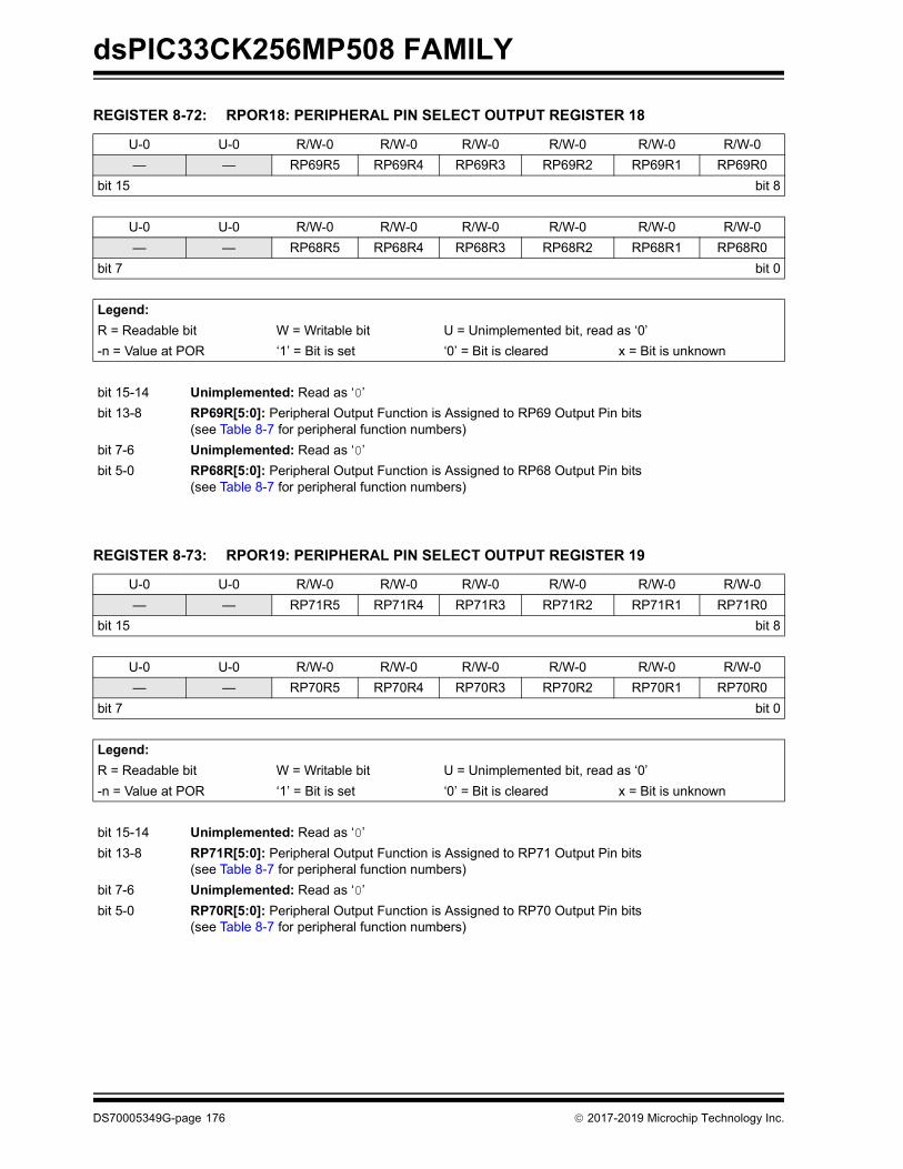
dsPIC33CK256MP508 FAMILY
REGISTER 8-72: RPOR18: PERIPHERAL PIN SELECT OUTPUT REGISTER 18
U-0 U-0 R/W-0 R/W-0 R/W-0 R/W-0 R/W-0 R/W-0— — RP69R5 RP69R4 RP69R3 RP69R2 RP69R1 RP69R0
bit 15 bit 8
U-0 U-0 R/W-0 R/W-0 R/W-0 R/W-0 R/W-0 R/W-0— — RP68R5 RP68R4 RP68R3 RP68R2 RP68R1 RP68R0
bit 7 bit 0
Legend:R = Readable bit W = Writable bit U = Unimplemented bit, read as ‘0’-n = Value at POR ‘1’ = Bit is set ‘0’ = Bit is cleared x = Bit is unknown
bit 15-14 Unimplemented: Read as ‘0’ bit 13-8 RP69R[5:0]: Peripheral Output Function is Assigned to RP69 Output Pin bits
(see Table 8-7 for peripheral function numbers)bit 7-6 Unimplemented: Read as ‘0’ bit 5-0 RP68R[5:0]: Peripheral Output Function is Assigned to RP68 Output Pin bits
(see Table 8-7 for peripheral function numbers)
REGISTER 8-73: RPOR19: PERIPHERAL PIN SELECT OUTPUT REGISTER 19
U-0 U-0 R/W-0 R/W-0 R/W-0 R/W-0 R/W-0 R/W-0— — RP71R5 RP71R4 RP71R3 RP71R2 RP71R1 RP71R0
bit 15 bit 8
U-0 U-0 R/W-0 R/W-0 R/W-0 R/W-0 R/W-0 R/W-0— — RP70R5 RP70R4 RP70R3 RP70R2 RP70R1 RP70R0
bit 7 bit 0
Legend:R = Readable bit W = Writable bit U = Unimplemented bit, read as ‘0’-n = Value at POR ‘1’ = Bit is set ‘0’ = Bit is cleared x = Bit is unknown
bit 15-14 Unimplemented: Read as ‘0’ bit 13-8 RP71R[5:0]: Peripheral Output Function is Assigned to RP71 Output Pin bits
(see Table 8-7 for peripheral function numbers)bit 7-6 Unimplemented: Read as ‘0’ bit 5-0 RP70R[5:0]: Peripheral Output Function is Assigned to RP70 Output Pin bits
(see Table 8-7 for peripheral function numbers)
DS70005349G-page 176 2017-2019 Microchip Technology Inc.

dsPIC33CK256MP508 FAMILY
REGISTER 8-74: RPOR20: PERIPHERAL PIN SELECT OUTPUT REGISTER 20
U-0 U-0 R/W-0 R/W-0 R/W-0 R/W-0 R/W-0 R/W-0— — RP73R5 RP73R4 RP73R3 RP73R2 RP73R1 RP73R0
bit 15 bit 8
U-0 U-0 R/W-0 R/W-0 R/W-0 R/W-0 R/W-0 R/W-0— — RP72R5 RP72R4 RP72R3 RP72R2 RP72R1 RP72R0
bit 7 bit 0
Legend:R = Readable bit W = Writable bit U = Unimplemented bit, read as ‘0’-n = Value at POR ‘1’ = Bit is set ‘0’ = Bit is cleared x = Bit is unknown
bit 15-14 Unimplemented: Read as ‘0’ bit 13-8 RP73R[5:0]: Peripheral Output Function is Assigned to RP73 Output Pin bits
(see Table 8-7 for peripheral function numbers)bit 7-6 Unimplemented: Read as ‘0’ bit 5-0 RP72R[5:0]: Peripheral Output Function is Assigned to RP72 Output Pin bits
(see Table 8-7 for peripheral function numbers)
REGISTER 8-75: RPOR21: PERIPHERAL PIN SELECT OUTPUT REGISTER 21
U-0 U-0 R/W-0 R/W-0 R/W-0 R/W-0 R/W-0 R/W-0— — RP75R5 RP75R4 RP75R3 RP75R2 RP75R1 RP75R0
bit 15 bit 8
U-0 U-0 R/W-0 R/W-0 R/W-0 R/W-0 R/W-0 R/W-0— — RP74R5 RP74R4 RP74R3 RP74R2 RP74R1 RP74R0
bit 7 bit 0
Legend:R = Readable bit W = Writable bit U = Unimplemented bit, read as ‘0’-n = Value at POR ‘1’ = Bit is set ‘0’ = Bit is cleared x = Bit is unknown
bit 15-14 Unimplemented: Read as ‘0’ bit 13-8 RP75R[5:0]: Peripheral Output Function is Assigned to RP75 Output Pin bits
(see Table 8-7 for peripheral function numbers)bit 7-6 Unimplemented: Read as ‘0’ bit 5-0 RP74R[5:0]: Peripheral Output Function is Assigned to RP74 Output Pin bits
(see Table 8-7 for peripheral function numbers)
2017-2019 Microchip Technology Inc. DS70005349G-page 177

dsPIC33CK256MP508 FAMILY
REGISTER 8-76: RPOR22: PERIPHERAL PIN SELECT OUTPUT REGISTER 22
U-0 U-0 R/W-0 R/W-0 R/W-0 R/W-0 R/W-0 R/W-0— — RP77R5 RP77R4 RP77R3 RP77R2 RP77R1 RP77R0
bit 15 bit 8
U-0 U-0 R/W-0 R/W-0 R/W-0 R/W-0 R/W-0 R/W-0— — RP76R5 RP76R4 RP76R3 RP76R2 RP76R1 RP76R0
bit 7 bit 0
Legend:R = Readable bit W = Writable bit U = Unimplemented bit, read as ‘0’-n = Value at POR ‘1’ = Bit is set ‘0’ = Bit is cleared x = Bit is unknown
bit 15-14 Unimplemented: Read as ‘0’ bit 13-8 RP77R[5:0]: Peripheral Output Function is Assigned to RP77 Output Pin bits
(see Table 8-7 for peripheral function numbers)bit 7-6 Unimplemented: Read as ‘0’ bit 5-0 RP76R[5:0]: Peripheral Output Function is Assigned to RP76 Output Pin bits
(see Table 8-7 for peripheral function numbers)
REGISTER 8-77: RPOR23: PERIPHERAL PIN SELECT OUTPUT REGISTER 23
U-0 U-0 R/W-0 R/W-0 R/W-0 R/W-0 R/W-0 R/W-0— — RP79R5 RP79R4 RP79R3 RP79R2 RP79R1 RP79R0
bit 15 bit 8
U-0 U-0 R/W-0 R/W-0 R/W-0 R/W-0 R/W-0 R/W-0— — RP78R5 RP78R4 RP78R3 RP78R2 RP78R1 RP78R0
bit 7 bit 0
Legend:R = Readable bit W = Writable bit U = Unimplemented bit, read as ‘0’-n = Value at POR ‘1’ = Bit is set ‘0’ = Bit is cleared x = Bit is unknown
bit 15-14 Unimplemented: Read as ‘0’ bit 13-8 RP79R[5:0]: Peripheral Output Function is Assigned to RP79 Output Pin bits
(see Table 8-7 for peripheral function numbers)bit 7-6 Unimplemented: Read as ‘0’ bit 5-0 RP78R[5:0]: Peripheral Output Function is Assigned to RP78 Output Pin bits
(see Table 8-7 for peripheral function numbers)
DS70005349G-page 178 2017-2019 Microchip Technology Inc.

dsPIC33CK256MP508 FAMILY
REGISTER 8-78: RPOR24: PERIPHERAL PIN SELECT OUTPUT REGISTER 24
U-0 U-0 R/W-0 R/W-0 R/W-0 R/W-0 R/W-0 R/W-0— — RP177R5(1) RP177R4(1) RP177R3(1) RP177R2(1) RP177R1(1) RP177R0(1)
bit 15 bit 8
U-0 U-0 R/W-0 R/W-0 R/W-0 R/W-0 R/W-0 R/W-0— — RP176R5(1) RP176R4(1) RP176R3(1) RP176R2(1) RP176R1(1) RP176R0(1)
bit 7 bit 0
Legend:R = Readable bit W = Writable bit U = Unimplemented bit, read as ‘0’-n = Value at POR ‘1’ = Bit is set ‘0’ = Bit is cleared x = Bit is unknown
bit 15-14 Unimplemented: Read as ‘0’ bit 13-8 RP177R[5:0]: Peripheral Output Function is Assigned to RP177 Output Pin bits(1)
(see Table 8-7 for peripheral function numbers)bit 7-6 Unimplemented: Read as ‘0’ bit 5-0 RP176R[5:0]: Peripheral Output Function is Assigned to RP176 Output Pin bits(1)
(see Table 8-7 for peripheral function numbers)
Note 1: These are virtual output ports.
REGISTER 8-79: RPOR25: PERIPHERAL PIN SELECT OUTPUT REGISTER 25
U-0 U-0 R/W-0 R/W-0 R/W-0 R/W-0 R/W-0 R/W-0— — RP179R5(1) RP179R4(1) RP179R3(1) RP179R2(1) RP179R1(1) RP179R0(1)
bit 15 bit 8
U-0 U-0 R/W-0 R/W-0 R/W-0 R/W-0 R/W-0 R/W-0— — RP178R5(1) RP178R4(1) RP178R3(1) RP178R2(1) RP178R1(1) RP178R0(1)
bit 7 bit 0
Legend:R = Readable bit W = Writable bit U = Unimplemented bit, read as ‘0’-n = Value at POR ‘1’ = Bit is set ‘0’ = Bit is cleared x = Bit is unknown
bit 15-14 Unimplemented: Read as ‘0’ bit 13-8 RP179R[5:0]: Peripheral Output Function is Assigned to RP179 Output Pin bits(1)
(see Table 8-7 for peripheral function numbers)bit 7-6 Unimplemented: Read as ‘0’ bit 5-0 RP178R[5:0]: Peripheral Output Function is Assigned to RP178 Output Pin bits(1)
(see Table 8-7 for peripheral function numbers)
Note 1: These are virtual output ports.
2017-2019 Microchip Technology Inc. DS70005349G-page 179

dsPIC33CK256MP508 FAMILY
REGISTER 8-80: RPOR26: PERIPHERAL PIN SELECT OUTPUT REGISTER 26
U-0 U-0 R/W-0 R/W-0 R/W-0 R/W-0 R/W-0 R/W-0— — RP181R5(1) RP181R4(1) RP181R3(1) RP181R2(1) RP181R1(1) RP181R0(1)
bit 15 bit 8
U-0 U-0 R/W-0 R/W-0 R/W-0 R/W-0 R/W-0 R/W-0— — RP180R5(1) RP180R4(1) RP180R3(1) RP180R2(1) RP180R1(1) RP180R0(1)
bit 7 bit 0
Legend:R = Readable bit W = Writable bit U = Unimplemented bit, read as ‘0’-n = Value at POR ‘1’ = Bit is set ‘0’ = Bit is cleared x = Bit is unknown
bit 15-14 Unimplemented: Read as ‘0’ bit 13-8 RP181R[5:0]: Peripheral Output Function is Assigned to RP181 Output Pin bits
(see Table 8-7 for peripheral function numbers)bit 7-6 Unimplemented: Read as ‘0’ bit 5-0 RP180R[5:0]: Peripheral Output Function is Assigned to RP180 Output Pin bits
(see Table 8-7 for peripheral function numbers)
Note 1: These are virtual output ports.
DS70005349G-page 180 2017-2019 Microchip Technology Inc.

2017-2019 M
icrochip Technology Inc.D
S70005349G-page 181
dsPIC33C
K256M
P508 FAM
ILY
TARe Bit 3 Bit 2 Bit 1 Bit 0
RP — — — —RP — — — —RP INT2R3 INT2R2 INT2R1 INT2R0RP — — — —RP TCKI1R3 TCKI1R2 TCKI1R1 TCKI1R0RP TCKI2R3 TCKI2R2 TCKI2R1 TCKI2R0RP TCKI3R3 TCKI3R2 TCKI3R1 TCKI3R0RP TCKI4R3 TCKI4R2 TCKI4R1 TCKI4R0RP TCKI5R3 TCKI5R2 TCKI5R1 TCKI5R0RP TCKI6R3 TCKI6R2 TCKI6R1 TCKI6R0RP TCKI7R3 TCKI7R2 TCKI7R1 TCKI7R0RP TCKI8R3 TCKI8R2 TCKI8R1 TCKI8R0RP OCFAR3 OCFAR2 OCFAR1 OCFAR0RP PCI8R3 PCI8R2 PCI8R1 PCI8R0RP PCI10R3 PCI10R2 PCI10R1 PCI10R0RP QEIA1R3 QEIA1R2 QEIA1R1 QEIA1R0RP 4 QEINDX1R3 QEINDX1R2 QEINDX1R1 QEINDX1R0RP QEIA2R3 QEIA2R2 QEIA2R1 QEIA2R0RP 4 QEINDX2R3 QEINDX2R2 QEINDX2R1 QEINDX2R0RP U1RXR3 U1RXR2 U1RXR1 U1RXR0RP U2RXR3 U2RXR2 U2RXR1 U2RXR0RP SDI1R3 SDI1R2 SDI1R1 SDI1R0RP SS1R3 SS1R2 SS1R1 SS1R0RP SDI2R3 SDI2R2 SDI2R1 SDI2R0RP SS2R3 SS2R2 SS2R1 SS2R0RP 4 CAN1RXR3 CAN1RXR2 CAN1RXR1 CAN1RXR0RP U3RXR3 U3RXR2 U3RXR1 U3RXR0RP SDI3R3 SDI3R2 SDI3R1 SDI3R0RP SS3R3 SS3R2 SS3R1 SS3R0RP — — — —RP ICM9R3 ICM9R2 ICM9R1 ICM9R0RP OCFCR3 OCFCR2 OCFCR1 OCFCR0RP PCI18R3 PCI18R2 PCI18R1 PCI18R0RP PCI12R3 PCI12R2 PCI12R1 PCI12R0RP PCI14R3 PCI14R2 PCI14R1 PCI14R0RP PCI16R3 PCI16R2 PCI16R1 PCI16R0RP SENT2R3 SENT2R2 SENT2R1 SENT2R0RP 4 CLCINBR3 CLCINBR2 CLCINBR1 CLCINBR0RP 4 CLCINDR3 CLCINDR2 CLCINDR1 CLCINDR0RP OCFDR3 OCFDR2 OCFDR1 OCFDR0RP U2CTSR3 U2CTSR2 U2CTSR1 U2CTSR0
BLE 8-13: PPS INPUT CONTROL REGISTERSgister Bit 15 Bit 14 Bit 13 Bit 12 Bit 11 Bit 10 Bit 9 Bit 8 Bit 7 Bit 6 Bit 5 Bit 4
CON — — — — IOLOCK — — — — — — —INR0 INT1R7 INT1R6 INT1R5 INT1R4 INT1R3 INT1R2 INT1R1 INT1R0 — — — —INR1 INT3R7 INT3R6 INT3R5 INT3R4 INT3R3 INT3R2 INT3R1 INT3R0 INT2R7 INT2R6 INT2R5 INT2R4INR2 T1CKR7 T1CKR6 T1CKR5 T1CKR4 T1CKR3 T1CKR2 T1CKR1 T1CKR0 — — — —INR3 ICM1R7 ICM1R6 ICM1R5 ICM1R4 ICM1R3 ICM1R2 ICM1R1 ICM1R0 TCKI1R7 TCKI1R6 TCKI1R5 TCKI1R4INR4 ICM2R7 ICM2R6 ICM2R5 ICM2R4 ICM2R3 ICM2R2 ICM2R1 ICM2R0 TCKI2R7 TCKI2R6 TCKI2R5 TCKI2R4INR5 ICM3R7 ICM3R6 ICM3R5 ICM3R4 ICM3R3 ICM3R2 ICM3R1 ICM3R0 TCKI3R7 TCKI3R6 TCKI3R5 TCKI3R4INR6 ICM4R7 ICM4R6 ICM4R5 ICM4R4 ICM4R3 ICM4R2 ICM4R1 ICM4R0 TCKI4R7 TCKI4R TCKI4R5 TCKI4R4INR7 ICM5R7 ICM5R6 ICM5R5 ICM5R4 ICM5R3 ICM5R2 ICM5R1 ICM5R0 TCKI5R7 TCKI5R6 TCKI5R5 TCKI5R4INR8 ICM6R7 ICM6R6 ICM6R5 ICM6R4 ICM6R3 ICM6R2 ICM6R1 ICM6R0 TCKI6R7 TCKI6R6 TCKI6R5 TCKI6R4INR9 ICM7R7 ICM7R6 ICM7R5 ICM7R4 ICM7R3 ICM7R2 ICM7R1 ICM7R0 TCKI7R7 TCKI7R6 TCKI7R5 TCKI7R4INR10 ICM8R7 ICM8R6 ICM8R5 ICM8R4 ICM8R3 ICM8R2 ICM8R1 ICM8R0 TCKI8R7 TCKI8R6 TCKI8R5 TCKI8R4INR11 OCFBR7 OCFBR6 OCFBR5 OCFBR4 OCFBR3 OCFBR2 OCFBR1 OCFBR0 OCFAR7 OCFAR6 OCFAR5 OCFAR4INR12 PCI9R7 PCI9R6 PCI9R5 PCI9R4 PCI9R3 PCI9R2 PCI9R1 PCI9R0 PCI8R7 PCI8R6 PCI8R5 PCI8R4INR13 PCI11R7 PCI11R6 PCI11R5 PCI11R4 PCI11R3 PCI11R2 PCI11R1 PCI11R0 PCI10R7 PCI10R6 PCI10R5 PCI10R4INR14 QEIB1R7 QEIB1R6 QEIB1R5 QEIB1R4 QEIB1R3 QEIB1R2 QEIB1R1 QEIB1R0 QEIA1R7 QEIA1R6 QEIA1R5 QEIA1R4INR15 QEIHOM1R7 QEIHOM1R6 QEIHOM1R5 QEIHOM1R4 QEIHOM1R3 QEIHOM1R2 QEIHOM1R1 QEIHOM1R0 QEINDX1R7 QEINDX1R6 QEINDX1R5 QEINDX1RINR16 QEIB2R7 QEIB2R6 QEIB2R5 QEIB2R4 QEIB2R3 QEIB2R2 QEIB2R1 QEIB2R0 QEIA2R7 QEIA2R6 QEIA2R5 QEIA2R4INR17 QEIHOM2R7 QEIHOM2R6 QEIHOM2R5 QEIHOM2R4 QEIHOM2R3 QEIHOM2R2 QEIHOM2R1 QEIHOM2R0 QEINDX2R7 QEINDX2R6 QEINDX2R5 QEINDX2RINR18 U1DSRR7 U1DSRR6 U1DSRR5 U1DSRR4 U1DSRR3 U1DSRR2 U1DSRR1 U1DSRR0 U1RXR7 U1RXR6 U1RXR5 U1RXR4INR19 U2DSRR7 U2DSRR6 U2DSRR5 U2DSRR4 U2DSRR3 U2DSRR2 U2DSRR1 U2DSRR0 U2RXR7 U2RXR6 U2RXR5 U2RXR4INR20 SCK1R7 SCK1R6 SCK1R5 SCK1R4 SCK1R3 SCK1R2 SCK1R1 SCK1R0 SDI1R7 SDI1R6 SDI1R5 SDI1R4INR21 REFOIR7 REFOIR6 REFOIR5 REFOIR4 REFOIR3 REFOIR2 REFOIR1 REFOIR0 SS1R7 SS1R6 SS1R5 SS1R4INR22 SCK2R7 SCK2R6 SCK2R5 SCK2R4 SCK2R3 SCK2R2 SCK2R1 SCK2R0 SDI2R7 SDI2R6 SDI2R5 SDI2R4INR23 — — — — — — — — SS2R7 SS2R6 SS2R5 SS2R4INR26 — — — — — — — — CAN1RXR7 CAN1RXR6 CAN1RXR5 CAN1RXRINR27 U3DSRR7 U3DSRR6 U3DSRR5 U3DSRR4 U3DSRR3 U3DSRR2 U3DSRR1 U3DSRR0 U3RXR7 U3RXR6 U3RXR5 U3RXR4INR29 SCK3R7 SCK3R6 SCK3R5 SCK3R4 SCK3R3 SCK3R2 SCK3R1 SCK3R0 SDI3R7 SDI3R6 SDI3R5 SDI3R4INR30 — — — — — — — — SS3R7 SS3R6 SS3R5 SS3R4INR32 TCKI9R7 TCKI9R6 TCKI9R5 TCKI9R4 TCKI9R3 TCKI9R2 TCKI9R1 TCKI9R0 — — — —INR33 — — — — — — — — ICM9R7 ICM9R6 ICM9R5 ICM9R4INR37 PCI17R7 PCI17R6 PCI17R5 PCI17R4 PCI17R3 PCI17R2 PCI17R1 PCI17R0 OCFCR7 OCFCR6 OCFCR5 OCFCR4INR38 — — — — — — — — PCI18R7 PCI18R6 PCI18R5 PCI18R4INR42 PCI13R7 PCI13R6 PCI13R5 PCI13R4 PCI13R3 PCI13R2 PCI13R1 PCI13R0 PCI12R7 PCI12R6 PCI12R5 PCI12R4INR43 PCI15R7 PCI15R6 PCI15R5 PCI15R4 PCI15R3 PCI15R2 PCI15R1 PCI15R0 PCI14R7 PCI14R6 PCI14R5 PCI14R4INR44 SENT1R7 SENT1R6 SENT1R5 SENT1R4 SENT1R3 SENT1R2 SENT1R1 SENT1R0 PCI16R7 PCI16R6 PCI16R5 PCI16R4INR45 CLCINAR7 CLCINAR6 CLCINAR5 CLCINAR4 CLCINAR3 CLCINAR2 CLCINAR1 CLCINAR0 SENT2R7 SENT2R6 SENT2R5 SENT2R4INR46 CLCINCR7 CLCINCR6 CLCINCR5 CLCINCR4 CLCINCR3 CLCINCR2 CLCINCR1 CLCINCR0 CLCINBR7 CLCINBR6 CLCINBR5 CLCINBRINR47 ADCTRGR7 ADCTRGR6 ADCTRGR5 ADCTRGR4 ADCTRGR3 ADCTRGR2 ADCTRGR1 ADCTRGR0 CLCINDR7 CLCINDR6 CLCINDR5 CLCINDRINR48 U1CTSR7 U1CTSR6 U1CTSR5 U1CTSR4 U1CTSR3 U1CTSR2 U1CTSR1 U1CTSR0 OCFDR7 OCFDR6 OCFDR5 OCFDR4INR49 U3CTSR7 U3CTSR6 U3CTSR5 U3CTSR4 U3CTSR3 U3CTSR2 U3CTSR1 U3CTSR0 U2CTSR7 U2CTSR6 U2CTSR5 U2CTSR4

dsPIC33C
K256M
P508 FAM
ILY
DS70005349G
-page 182
2017-2019 Microchip Technology Inc.
it 4 Bit 3 Bit 2 Bit 1 Bit 0
32R4 RP32R3 RP32R2 RP32R1 RP32R0
34R4 RP34R3 RP34R2 RP34R1 RP34R0
36R4 RP36R3 RP36R2 RP36R1 RP36R0
38R4 RP38R3 RP38R2 RP38R1 RP38R0
40R4 RP40R3 RP40R2 RP40R1 RP40R0
42R4 RP42R3 RP42R2 RP42R1 RP42R0
44R4 RP44R3 RP44R2 RP44R1 RP44R0
46R4 RP46R3 RP46R2 RP46R1 RP46R0
48R4 RP48R3 RP48R2 RP48R1 RP48R0
50R4 RP50R3 RP50R2 RP50R1 RP50R0
52R4 RP52R3 RP52R2 RP52R1 RP52R0
54R4 RP54R3 RP54R2 RP54R1 RP54R0
56R4 RP56R3 RP56R2 RP56R1 RP56R0
58R4 RP58R3 RP58R2 RP58R1 RP58R0
60R4 RP60R3 RP60R2 RP60R1 RP60R0
62R4 RP62R3 RP62R2 RP62R1 RP62R0
64R4 RP64R3 RP64R2 RP64R1 RP64R0
66R4 RP66R3 RP66R2 RP66R1 RP66R0
68R4 RP68R3 RP68R2 RP68R1 RP68R0
70R4 RP70R3 RP70R2 RP70R1 RP70R0
72R4 RP72R3 RP72R2 RP72R1 RP72R0
74R4 RP74R3 RP74R2 RP74R1 RP74R0
76R4 RP76R3 RP76R2 RP76R1 RP76R0
78R4 RP78R3 RP78R2 RP78R1 RP78R0
176R4 RP176R3 RP176R2 RP176R1 RP176R0
178R4 RP178R3 RP178R2 RP178R1 RP178R0
180R4 RP180R3 RP180R2 RP180R1 RP180R0
TABLE 8-14: PPS OUTPUT CONTROL REGISTERSRegister Bit 15 Bit 14 Bit 13 Bit 12 Bit 11 Bit 10 Bit 9 Bit 8 Bit 7 Bit 6 Bit 5 B
RPOR0 — — RP33R5 RP33R4 RP33R3 RP33R2 RP33R1 RP33R0 — — RP32R5 RP
RPOR1 — — RP35R5 RP35R4 RP35R3 RP35R2 RP35R1 RP35R0 — — RP34R5 RP
RPOR2 — — RP37R5 RP37R4 RP37R3 RP37R2 RP37R1 RP37R0 — — RP36R5 RP
RPOR3 — — RP39R5 RP39R4 RP39R3 RP39R2 RP39R1 RP39R0 — — RP38R5 RP
RPOR4 — — RP41R5 RP41R4 RP41R3 RP41R2 RP41R1 RP41R0 — — RP40R5 RP
RPOR5 — — RP43R5 RP43R4 RP43R3 RP43R2 RP43R1 RP43R0 — — RP42R5 RP
RPOR6 — — RP45R5 RP45R4 RP45R3 RP45R2 RP45R1 RP45R0 — — RP44R5 RP
RPOR7 — — RP47R5 RP47R4 RP47R3 RP47R2 RP47R1 RP47R0 — — RP46R5 RP
RPOR8(1) — — RP49R5 RP49R4 RP49R3 RP49R2 RP49R1 RP49R0 — — RP48R5 RP
RPOR9(1) — — RP51R5 RP51R4 RP51R3 RP51R2 RP51R1 RP51R0 — — RP50R5 RP
RPOR10(1) — — RP53R5 RP53R4 RP53R3 RP53R2 RP53R1 RP53R0 — — RP52R5 RP
RPOR11(1) — — RP55R5 RP55R4 RP55R3 RP55R2 RP55R1 RP55R0 — — RP54R5 RP
RPOR12(1) — — RP57R5 RP57R4 RP57R3 RP57R2 RP57R1 RP57R0 — — RP56R5 RP
RPOR13(1) — — RP59R5 RP59R4 RP59R3 RP59R2 RP59R1 RP59R0 — — RP58R5 RP
RPOR14(1) — — RP61R5 RP61R4 RP61R3 RP61R2 RP61R1 RP61R0 — — RP60R5 RP
RPOR15(1) — — RP63R5 RP63R4 RP63R3 RP63R2 RP63R1 RP63R0 — — RP62R5 RP
RPOR16(1) — — RP65R5 RP65R4 RP65R3 RP65R2 RP65R1 RP65R0 — — RP64R5 RP
RPOR17(1) — — RP67R5 RP67R4 RP67R3 RP67R2 RP67R1 RP67R0 — — RP66R5 RP
RPOR18(1) — — RP69R5 RP69R4 RP69R3 RP69R2 RP69R1 RP69R0 — — RP68R5 RP
RPOR19(1) — — RP71R5 RP71R4 RP71R3 RP71R2 RP71R1 RP71R0 — — RP70R5 RP
RPOR20(1) — — RP73R5 RP73R4 RP73R3 RP73R2 RP73R1 RP73R0 — — RP72R5 RP
RPOR21(1) — — RP75R5 RP75R4 RP75R3 RP75R2 RP75R1 RP75R0 — — RP74R5 RP
RPOR22(1) — — RP77R5 RP77R4 RP77R3 RP77R2 RP77R1 RP77R0 — — RP76R5 RP
RPOR23(1) — — RP79R5 RP79R4 RP79R3 RP79R2 RP79R1 RP79R0 — — RP78R5 RP
RPOR24 — — RP177R5 RP177R4 RP177R3 RP177R2 RP177R1 RP177R0 — — RP176R5 RP
RPOR25 — — RP179R5 RP179R4 RP179R3 RP179R2 RP179R1 RP179R0 — — RP178R5 RP
RPOR26 — — RP181R5 RP181R4 RP181R3 RP181R2 RP181R1 RP181R0 — — RP180R5 RP
Note 1: Availability is dependent on supported I/O ports. Refer to Table 8-1 and Table 8-6 for availability on device variants.

dsPIC33CK256MP508 FAMILY
9.0 OSCILLATOR WITH HIGH-FREQUENCY PLL
The dsPIC33CK256MP508 family oscillator withhigh-frequency PLL includes these characteristics:• On-Chip Phase-Locked Loop (PLL) to Boost
Internal Operating Frequency on Select Internal and External Oscillator Sources
• Auxiliary PLL (APLL) Clock Generator to Boost Operating Frequency for Peripherals
• Doze mode for System Power Savings
• Scalable Reference Clock Output (REFCLKO) • On-the-Fly Clock Switching between Various
Clock Sources• Fail-Safe Clock Monitoring (FSCM) that Detects
Clock Failure and Permits Safe Application Recovery or Shutdown
A block diagram of the dsPIC33CK256MP508 oscillatorsystem is shown in Figure 9-1.
FIGURE 9-1: dsPIC33CK256MP508 CORE CLOCK SOURCES BLOCK DIAGRAM
Note 1: This data sheet summarizes the featuresof the dsPIC33CK256MP508 family ofdevices. It is not intended to be a compre-hensive reference source. To complementthe information in this data sheet, refer to“Oscillator Module with High-SpeedPLL” (www.microchip.com/DS70005255)in the “dsPIC33/PIC24 Family ReferenceManual”.
BFRCCLK
FRCCLK
POSCCLK
LPRCCLKFRC
8 MHz
POSC
LPRC32 kHz
OSCO
OSCI
TUN[5:0]
FCY
FP
FOSC
VCO Outputs
APLL and
REFCLKO
AVCO Outputs
Core ClockSelection and
PLL/DIVSubsystem
BFRC8 MHz
2017-2019 Microchip Technology Inc. DS70005349G-page 183

dsPIC33CK256MP508 FAMILY
FIGURE 9-2: dsPIC33CK256MP508 CORE OSCILLATOR SUBSYSTEM
Note 1: See Figure 9-3 for details of the PLL module.2: See Figure 9-3 for the source of FVCO.3: See Figure 9-3 for the source of AVCO.4: XTPLL, HSPLL, ECPLL, FRCPLL (FPLLO).5: Clock option for PWM.6: Clock option for ADC.7: Clock option for DAC.
FRCCLK
POSCCLK
S1
S3PLL(1)
REFCLKO
DO
ZE FCY
FRC
DIV
N
FRCDIVN
RODIV[14:0]
÷ N
ROSEL[3:0]
REFIFVCO/4BFRCLPRC
FRCPOSC
FPFOSC
POSCCLK
FRC
FRCSEL
APLL AFPLLO(5,7)
AFVCO(3)
Auxiliary PLL
S6 FNOSC[2:0]NOSC[2:0]
S2
S1/S3
S0
S7
S6
S5
FOSC
DOZE[2:0]
FP
ResetClock Clock
SwitchFail
FRCDIV[2:0]
FRCCLK
FVCO(2)
POSCCLK
FPLLO/2(4)
FRCCLK
BFRCCLK
LPRCCLK
FVCO
FVCODIV
VCODIV[1:0]
FVCO/2(7)
FVCO/3FVCO/4(6)
AVCODivider
AFVCO
AFVCODIV(6)
AVCODIV[1:0]
AFVCO/2(5,7)
AFVCO/3AFVCO/4
÷ 2
No ClockFVCO
FPLLOFVCO/2FVCO/3FVCO/4
AFVCOAFVCO/2AFVCO/3AFVCO/4
÷ N FCAN
CANCLKSEL[3:0]
CANDIV[6:0]
CAN Clock Generation
AFPLLO
÷ 2
FPLLO(5,7)
VCODivider
DS70005349G-page 184 2017-2019 Microchip Technology Inc.

dsPIC33CK256MP508 FAMILY
9.1 Primary PLLThe Primary Oscillator and internal FRC Oscillatorsources can optionally use an on-chip PLL to obtainhigher operating speeds. Figure 9-3 illustrates a blockdiagram of the PLL module.
For PLL operation, the following requirements must bemet at all times without exception:• The PLL Input Frequency (FPLLI) must be in the
range of 8 MHz to 64 MHz• The PFD Input Frequency (FPFD) must be in the
range of 8 MHz to (FVCO/16) MHzThe VCO Output Frequency (FVCO) must be in therange of 400 MHz to 1600 MHz
FIGURE 9-3: PLL AND VCO DETAIL
DIV1-8
PFD LockDetect
DIV1-7
DIV1-7
FeedbackDivider16-200
VCODivider
FVCO
FVCO
FVCODIVPLLFBDIV[7:0]
PLLPRE[3:0]POST1DIV[2:0]
POST2DIV[2:0]
FPLLO(1,3)
PLL Ready(LOCK)
FRCCLK(4)
POSCCLK
Note 1: Clock option for PWM.2: Clock option for ADC.3: Clock option for DAC.4: PLL source is always FRC unless FNOSC is the Primary Oscillator with PLL.
S1
S3
VCODIV[1:0]
FVCO/2(3)
FVCO/3FVCO/4(2)
VCO
2017-2019 Microchip Technology Inc. DS70005349G-page 185

dsPIC33CK256MP508 FAMILY
Equation 9-1 provides the relationship between thePLL Input Frequency (FPLLI) and VCO OutputFrequency (FVCO).
EQUATION 9-1: FVCO CALCULATION
Equation 9-2 provides the relationship between the PLLInput Frequency (FPLLI) and PLL Output Frequency(FPLLO).
EQUATION 9-2: FPLLO CALCULATION
EXAMPLE 9-1: CODE EXAMPLE FOR USING PRIMARY PLL WITH 8 MHz INTERNAL FRC
FVCO = FPLLI = FPLLI PLLFBDIV[7:0]PLLPRE[3:0]
MN1
Note: The PLL Phase Detector Input Divider Select (PLLPREx) bits and the PLL Feedback Divider (PLLFBDIVx)bits should not be changed when operating in PLL mode. Therefore, the user must start in either a non-PLL mode or clock switch to a non-PLL mode (e.g., internal FRC Oscillator) to make any necessarychanges and then clock switch to the desired PLL mode.It is not permitted to directly clock switch from one PLL clock source to a different PLL clock source. Theuser would need to transition between PLL clock sources with a clock switch to a non-PLL clock source.
Where:M = PLLFBDIV[7:0] N1 = PLLPRE[3:0]N2 = POST1DIV[2:0]N3 = POST2DIV[2:0]
FPLLO = FPLLI = FPLLI PLLFBDIV[7:0]PLLPRE[3:0] POST1DIV[2:0]POST2DIV[2:0]
MN1 N2N3
//code example for 50 MIPS system clock using 8MHz FRC// Select FRC on POR#pragma config FNOSC = FRC // Oscillator Source Selection (Internal Fast RC (FRC))#pragma config IESO = OFF // Enable Clock Switching#pragma config FCKSM = CSECMDint main(){// Configure PLL prescaler, both PLL postscalers, and PLL feedback dividerCLKDIVbits.PLLPRE = 1; // N1=1PLLFBDbits.PLLFBDIV = 125; // M = 125PLLDIVbits.POST1DIV = 5; // N2=5PLLDIVbits.POST2DIV = 1; // N3=1// Initiate Clock Switch to FRC with PLL (NOSC=0b001)__builtin_write_OSCCONH(0x01);__builtin_write_OSCCONL(OSCCON | 0x01);// Wait for Clock switch to occurwhile (OSCCONbits.OSWEN!= 0);}
DS70005349G-page 186 2017-2019 Microchip Technology Inc.

dsPIC33CK256MP508 FAMILY
9.2 Auxiliary PLLThe dsPIC33CK256MP508 device family implementsan Auxiliary PLL (APLL) module, which is used togenerate various peripheral clock sources independentof the system clock. Figure 9-4 shows a block diagramof the APLL module.
For APLL operation, the following requirements mustbe met at all times without exception:• The APLL Input Frequency (AFPLLI) must be in
the range of 8 MHz to 64 MHz• The APFD Input Frequency (AFPFD) must be in
the range of 8 MHz to (AFVCO/16) MHz• The AVCO Output Frequency (AFVCO) must be in
the range of 400 MHz to 1600 MHz
FIGURE 9-4: APLL AND VCO DETAIL
DIV1-8 APFD Lock
Detect AVCO DIV1-7
DIV1-7
FeedbackDivider16-200
FRCSEL AFVCO
APLLFBDIV[7:0]
APLLPRE[3:0]
APOST1DIV[2:0]APOST2DIV[2:0]APLL Ready
(APLLCLK)
FRCCLK
POSCCLK
Note 1: Clock option for PWM.2: Clock option for ADC.3: Clock option for DAC.
AVCODivider
AFVCO
AFVCODIV(2)
AVCODIV[1:0]
AFVCO/2(1,3)
AFVCO/3AFVCO/4
0
1
AFPLLO(1,3)
APLLEN
2017-2019 Microchip Technology Inc. DS70005349G-page 187

dsPIC33CK256MP508 FAMILY
Equation 9-3 provides the relationship between theAPLL Input Frequency (AFPLLI) and the AVCO OutputFrequency (AFVCO).
EQUATION 9-3: AFVCO CALCULATION
Equation 9-4 provides the relationship between theAPLL Input Frequency (AFPLLI) and APLL OutputFrequency (AFPLLO).
EQUATION 9-4: AFPLLO CALCULATION
EXAMPLE 9-2: CODE EXAMPLE FOR USING AUXILIARY PLL WITH THE INTERNAL FRC OSCILLATOR
AFVCO = AFPLLI = AFPLLI APLLFBDIV[7:0]APLLPRE[3:0]
MN1
Note: Even with the APLLEN bit set, another peripheral must generate a clock request before the APLL will start.
Where:M = APLLFBDIV[7:0] N1 = APLLPRE[3:0] N2 = APOST1DIV[2:0] N3 = APOST2DIV[2:0]
AFPLLO = AFPLLI = AFPLLI APLLFBDIV[7:0]APLLPRE[3:0] POST1DIV[2:0]POST2DIV[2:0]
MN1 N2N3
//code example for AFVCO = 1 GHz and AFPLLO = 500 MHz using 8 MHz internal FRC// Configure the source clock for the APLLACLKCON1bits.FRCSEL = 1; // Select internal FRC as the clock source// Configure the APLL prescaler, APLL feedback divider, and both APLL postscalers.ACLKCON1bits.APLLPRE = 1; // N1 = 1APLLFBD1bits.APLLFBDIV = 125; // M = 125APLLDIV1bits.APOST1DIV = 2; // N2 = 2APLLDIV1bits.APOST2DIV = 1; // N3 = 1// Enable APLLACLKCON1bits.APLLEN = 1;
DS70005349G-page 188 2017-2019 Microchip Technology Inc.

dsPIC33CK256MP508 FAMILY
9.3 CPU ClockingThe dsPIC33CK256MP508 devices can be configured touse any of the following clock configurations:• Primary Oscillator (POSC) on the OSCI and
OSCO pins• Internal Fast RC Oscillator (FRC) with optional
clock divider • Internal Low-Power RC Oscillator (LPRC)• Primary Oscillator with PLL (ECPLL, HSPLL, XTPLL)• Internal Fast RC Oscillator with PLL (FRCPLL)• Backup Internal Fast RC Oscillator (BFRC)
The system clock source is divided by two to producethe internal instruction cycle clock. In this document,the instruction cycle clock is denoted by FCY. Thetiming diagram in Figure 9-5 illustrates the relationshipbetween the system clock (FOSC), the instruction cycleclock (FCY) and the Program Counter (PC).The internal instruction cycle clock (FCY) can beoutput on the OSCO I/O pin if the Primary Oscillatormode (POSCMD[1:0]) is not configured as HS/XT. Formore information, see Section 9.0 “Oscillator withHigh-Frequency PLL”.
FIGURE 9-5: CLOCK AND INSTRUCTION CYCLE TIMING
PC + 2 PC + 4
Fetch INST (PC)
Execute INST (PC – 2) Fetch INST (PC + 2)
Execute INST (PC) Fetch INST (PC + 4)
Execute INST (PC + 2)
TCY
FOSC
FCY
PC PC
2017-2019 Microchip Technology Inc. DS70005349G-page 189

dsPIC33CK256MP508 FAMILY
9.4 Primary Oscillator (POSC)The dsPIC33CK256MP508 family devices feature aPrimary Oscillator (POSC) and it is available on theOSCI and OSCO pins. This connection enables anexternal crystal (or ceramic resonator) to provide theclock to the device. The Primary Oscillator providesthree modes of operation:• Medium Speed Oscillator (XT Mode):
The XT mode is a Medium Gain, Medium Frequency mode used to work with crystal frequencies of 3.5 MHz to 10 MHz.
• High-Speed Oscillator (HS Mode):The HS mode is a High-Gain, High-Frequency mode used to work with crystal frequencies of 10 MHz to 32 MHz.
• External Clock Source Operation (EC Mode):If the on-chip oscillator is not used, the EC mode allows the internal oscillator to be bypassed. The device clocks are generated from an external source (0 MHz to up to 64 MHz) and input on the OSCI pin.
Example 9-3 illustrates code for using the PLL(50 MIPS) with the Primary Oscillator.
EXAMPLE 9-3: CODE EXAMPLE FOR USING PLL (50 MIPS) WITH PRIMARY OSCILLATOR (POSC)//code example for 50 MIPS system clock using POSC with 10 MHz external crystal
// Select FRC on POR#pragma config FNOSC = FRC // Oscillator Source Selection (Internal Fast RC (FRC))#pragma config IESO = OFF /// Enable Clock Switching and Configure POSC in XT mode#pragma config POSCMD = XT #pragma config FCKSM = CSECMD
int main(){
// Configure PLL prescaler, both PLL postscalers, and PLL feedback dividerCLKDIVbits.PLLPRE = 1; // N1=1PLLFBDbits.PLLFBDIV = 100; // M = 100 PLLDIVbits.POST1DIV = 5; // N2=5PLLDIVbits.POST2DIV = 1; // N3=1
// Initiate Clock Switch to Primary Oscillator with PLL (NOSC=0b011)__builtin_write_OSCCONH(0x03);__builtin_write_OSCCONL(OSCCON | 0x01);
// Wait for Clock switch to occurwhile (OSCCONbits.OSWEN!= 0);
// Wait for PLL to lockwhile (OSCCONbits.LOCK!= 1);
}
DS70005349G-page 190 2017-2019 Microchip Technology Inc.

dsPIC33CK256MP508 FAMILY
9.5 Internal Fast RC (FRC) OscillatorThe dsPIC33CK256MP508 family devices contain oneinstance of the internal Fast RC (FRC) Oscillator and itprovides a nominal 8 MHz clock without requiring anexternal crystal or ceramic resonator, which results insystem cost savings for applications that do not requirea precise clock reference.The application software can tune the frequency ofthe oscillator using the FRC Oscillator Tuning bits(TUN[5:0]) in the FRC Oscillator Tuning register(OSCTUN[5:0]).
9.6 Low-Power RC (LPRC) OscillatorThe dsPIC33CK256MP508 family devices contain oneinstance of the Low-Power RC (LPRC) Oscillator and itprovides a nominal clock frequency of 32 kHz, and isthe clock source for the Power-up Timer (PWRT),Watchdog Timer (WDT) and Fail-Safe Clock Monitor(FSCM) circuits in the clock subsystem.The LPRC Oscillator is the clock source for the PWRT,WDT and FSCM. The LPRC Oscillator is enabled atpower-on.The LPRC Oscillator remains enabled under theseconditions:• The FSCM is enabled• The WDT is enabled• The LPRC Oscillator is selected as the system clock
If none of these conditions is true, the LPRC Oscillatorshuts off after the PWRT expires. The LPRC Oscillatoris shut off in Sleep mode.
9.7 Backup Internal Fast RC (BFRC) Oscillator
The oscillator block provides a stable reference clocksource for the Fail-Safe Clock Monitor (FSCM). WhenFSCM is enabled in the FCKSM[1:0] Configuration bits(FOSC[7:6]), it constantly monitors the main clocksource against a reference signal from the 8 MHzBackup Internal Fast RC (BFRC) Oscillator. In case ofa clock failure, the Fail-Safe Clock Monitor switches theclock to the BFRC Oscillator, allowing for continuedlow-speed operation or a safe application shutdown.
9.8 Reference Clock OutputIn addition to the CLKO output (FOSC/2), thedsPIC33CK256MP508 family devices can be configuredto provide a reference clock output signal to a port pin.This feature is available in all oscillator configurationsand allows the user to select a greater range of clock sub-multiples to drive external devices in the application.CLKO is enabled by Configuration bit, OSCIOFNC, andis independent of the REFCLKO reference clock.REFCLKO is mappable to any I/O pin that has mappedoutput capability. Refer to Table 8-7 for more information.The Reference Clock Output module block diagram isshown in Figure 9-6.
FIGURE 9-6: REFERENCE CLOCK GENERATOR
REFCLKO (PPS)
ROOUT
To SPI,RODIV[14:0]
REFCLKI (PPS) PinFVCO/4BFRCLPRC
Primary OscillatorPeripheral Clock (FP)
ROSEL[3:0]
CCP, CLCSystem Clock (FOSC)
FRC
10000110010101000011001000010000
ROTRIM[8:0]
Divider
2017-2019 Microchip Technology Inc. DS70005349G-page 191

dsPIC33CK256MP508 FAMILY
This reference clock output is controlled by theREFOCONL and REFOCONH registers. Setting theROEN bit (REFOCONL[15]) makes the clock signalavailable on the REFCLKO pin. The RODIV[14:0]bits (REFOCONH[14:0]) and ROTRIM[8:0] bits(REFOTRIM[15:7]) enable the selection of differentclock divider options. The formula for determining thefinal frequency output is shown in Equation 9-5. TheROSWEN bit (REFOCONL[9]) indicates that the clockdivider has been successfully switched. In order toswitch the REFCLKO divider, the user should ensurethat this bit reads as ‘0’. Write the updated values to theRODIV[14:0] or ROTRIM[8:0] bits, set the ROSWEN bitand then wait until it is cleared before assuming that theREFCLKO clock is valid.
EQUATION 9-5: CALCULATING FREQUENCY OUTPUT
The ROSEL[3:0] bits (REFOCONL[3:0]) determinewhich clock source is used for the reference clock out-put. The ROSLP bit (REFOCONL[11]) determines if thereference source is available on REFCLKO when thedevice is in Sleep mode.To use the reference clock output in Sleep mode, boththe ROSLP bit must be set and the clock selected by theROSEL[3:0] bits must be enabled for operation duringSleep mode, if possible. Clearing the ROSEL[3:0] bitsallows the reference output frequency to change, as thesystem clock changes, during any clock switches. TheROOUT bit enables/disables the reference clock outputon the REFCLKO pin.The ROACTIV bit (REFOCONL[8]) indicates that themodule is active; it can be cleared by disabling themodule (setting ROEN to ‘0’). The user must notchange the reference clock source, or adjust the dividerwhen the ROACTIV bit indicates that the module isactive. To avoid glitches, the user should not disablethe module until the ROACTIV bit is ‘1’.
Where: FREFOUT = Output FrequencyFREFIN = Input FrequencyWhen RODIV[14:0] = 0, the output clock isthe same as the input clock.
FREFOUT =FREFIN
2 • (RODIV[14:0] + ROTRIM[8:0]/512)
DS70005349G-page 192 2017-2019 Microchip Technology Inc.

dsPIC33CK256MP508 FAMILY
9.9 Oscillator ConfigurationThe oscillator system has both Configuration registersand SFRs to configure, control and monitor the system.The FOSCSEL and FOSC Configuration registers(Register 30-4 and Register 30-5, respectively) areused for initial setup.
Table 9-1 lists the configuration settings that select thedevice’s oscillator source and operating mode at aPower-on Reset (POR).
9.10 OSCCON Unlock SequenceThe OSCCON register is protected against unintendedwrites through a lock mechanism. The upper and lowerbytes of OSCCON have their own unlock sequence,and both must be used when writing to both bytes of theregister.Before OSCCON can be written to, the following unlocksequence must be used:1. Execute the unlock sequence for the OSCCON
high byte.In two back-to-back instructions:• Write 0x78 to OSCCON[15:8]• Write 0x9A to OSCCON[15:8]
2. In the instruction immediately following theunlock sequence, the OSCCON[10:8] bits canbe modified.
3. Execute the unlock sequence for the OSCCONlow byte.In two back-to-back instructions:• Write 0x46 to OSCCON[7:0]• Write 0x57 to OSCCON[7:0]
4. In the instruction immediately following theunlock sequence, the OSCCON[7:0] bits can bemodified.
TABLE 9-1: CONFIGURATION BIT VALUES FOR CLOCK SELECTIONOscillator
Source Oscillator Mode FNOSC[2:0]Value
POSCMD[1:0]Value Notes
S0 Fast RC Oscillator (FRC) 000 xx 1S1 Fast RC Oscillator with PLL (FRCPLL) 001 xx 1S2 Primary Oscillator (EC) 010 00 1S2 Primary Oscillator (XT) 010 01S2 Primary Oscillator (HS) 010 10S3 Primary Oscillator with PLL (ECPLL) 011 00 1S3 Primary Oscillator with PLL (XTPLL) 011 01S3 Primary Oscillator with PLL (HSPLL) 011 10S4 Reserved 100 xxS5 Low-Power RC Oscillator (LPRC) 101 xx 1S6 Backup FRC (BFRC) 110 xx 1S7 Fast RC Oscillator with ÷ N Divider
(FRCDIVN)111 xx 1, 2
Note 1: The OSCO pin function is determined by the OSCIOFNC Configuration bit.2: This is the default oscillator mode for an unprogrammed (erased) device.
Note: MPLAB® XC16 provides built-in C languagefunction for unlocking the OSCCON register:__builtin_write_OSCCONH(value)__builtin_write_OSCCONL(OSCCON | value)For more information, see the “MPLAB® XC16C Compiler User’s Guide” (DS50002071).
2017-2019 Microchip Technology Inc. DS70005349G-page 193

dsPIC33CK256MP508 FAMILY
9.11 Oscillator Control Registers
REGISTER 9-1: OSCCON: OSCILLATOR CONTROL REGISTER(1)
U-0 R-0 R-0 R-0 U-0 R/W-y R/W-y R/W-y— COSC2 COSC1 COSC0 — NOSC2(2) NOSC1(2) NOSC0(2)
bit 15 bit 8
R/W-0 U-0 R-0 U-0 R/W-0 U-0 U-0 R/W-0CLKLOCK — LOCK — CF(3) — — OSWEN
bit 7 bit 0
Legend: y = Value set from Configuration bits on PORR = Readable bit W = Writable bit U = Unimplemented bit, read as ‘0’-n = Value at POR ‘1’ = Bit is set ‘0’ = Bit is cleared x = Bit is unknown
bit 15 Unimplemented: Read as ‘0’bit 14-12 COSC[2:0]: Current Oscillator Selection bits (read-only)
111 = Fast RC Oscillator (FRC) with Divide-by-n (FRCDIVN)110 = Backup FRC (BFRC)101 = Low-Power RC Oscillator (LPRC)100 = Reserved – default to FRC011 = Primary Oscillator (XT, HS, EC) with PLL (XTPLL, HSPLL, ECPLL)010 = Primary Oscillator (XT, HS, EC)001 = Fast RC Oscillator (FRC) with PLL (FRCPLL) 000 = Fast RC Oscillator (FRC)
bit 11 Unimplemented: Read as ‘0’bit 10-8 NOSC[2:0]: New Oscillator Selection bits(2)
111 = Fast RC Oscillator (FRC) with Divide-by-n (FRCDIVN)110 = Backup FRC (BFRC)101 = Low-Power RC Oscillator (LPRC)100 = Reserved – default to FRC011 = Primary Oscillator (XT, HS, EC) with PLL (XTPLL, HSPLL, ECPLL)010 = Primary Oscillator (XT, HS, EC)001 = Fast RC Oscillator (FRC) with PLL (FRCPLL)000 = Fast RC Oscillator (FRC)
bit 7 CLKLOCK: Clock Lock Enable bit 1 = If (FCKSM0 = 1), then clock and PLL configurations are locked; if (FCKSM0 = 0), then clock and
PLL configurations may be modified0 = Clock and PLL selections are not locked, configurations may be modified
bit 6 Unimplemented: Read as ‘0’bit 5 LOCK: PLL Lock Status bit (read-only)
1 = Indicates that PLL is in lock or PLL start-up timer is satisfied0 = Indicates that PLL is out of lock, start-up timer is in progress or PLL is disabled
bit 4 Unimplemented: Read as ‘0’
Note 1: Writes to this register require an unlock sequence (see Section 9.10 “OSCCON Unlock Sequence”). 2: Direct clock switches between any Primary Oscillator mode with PLL and FRCPLL mode are not permit-
ted. This applies to clock switches in either direction. In these instances, the application must switch to FRC mode as a transitional clock source between the two PLL modes.
3: This bit should only be cleared in software. Setting the bit in software (= 1) will have the same effect as an actual oscillator failure and will trigger an oscillator failure trap.
DS70005349G-page 194 2017-2019 Microchip Technology Inc.

dsPIC33CK256MP508 FAMILY
bit 3 CF: Clock Fail Detect bit(3)
1 = FSCM has detected a clock failure0 = FSCM has not detected a clock failure
bit 2-1 Unimplemented: Read as ‘0’bit 0 OSWEN: Oscillator Switch Enable bit
1 = Requests oscillator switch to the selection specified by the NOSC[2:0] bits0 = Oscillator switch is complete
REGISTER 9-1: OSCCON: OSCILLATOR CONTROL REGISTER(1) (CONTINUED)
Note 1: Writes to this register require an unlock sequence (see Section 9.10 “OSCCON Unlock Sequence”). 2: Direct clock switches between any Primary Oscillator mode with PLL and FRCPLL mode are not permit-
ted. This applies to clock switches in either direction. In these instances, the application must switch to FRC mode as a transitional clock source between the two PLL modes.
3: This bit should only be cleared in software. Setting the bit in software (= 1) will have the same effect as an actual oscillator failure and will trigger an oscillator failure trap.
2017-2019 Microchip Technology Inc. DS70005349G-page 195

dsPIC33CK256MP508 FAMILY
REGISTER 9-2: CLKDIV: CLOCK DIVIDER REGISTER
R/W-0 R/W-0 R/W-1 R/W-1 R/W-0 R/W-0 R/W-0 R/W-0ROI DOZE2(1) DOZE1(1) DOZE0(1) DOZEN(2,3) FRCDIV2 FRCDIV1 FRCDIV0
bit 15 bit 8
U-0 U-0 r-0 r-0 R/W-0 R/W-0 R/W-0 R/W-1— — — — PLLPRE[3:0](4)
bit 7 bit 0
Legend: r = Reserved bitR = Readable bit W = Writable bit U = Unimplemented bit, read as ‘0’-n = Value at POR ‘1’ = Bit is set ‘0’ = Bit is cleared x = Bit is unknown
bit 15 ROI: Recover on Interrupt bit1 = Interrupts will clear the DOZEN bit and the processor clock, and the peripheral clock ratio is set to 1:10 = Interrupts have no effect on the DOZEN bit
bit 14-12 DOZE[2:0]: Processor Clock Reduction Select bits(1) 111 = FP divided by 128110 = FP divided by 64101 = FP divided by 32100 = FP divided by 16011 = FP divided by 8 (default)010 = FP divided by 4001 = FP divided by 2000 = FP divided by 1
bit 11 DOZEN: Doze Mode Enable bit(2,3)
1 = DOZE[2:0] field specifies the ratio between the peripheral clocks and the processor clocks0 = Processor clock and peripheral clock ratio is forced to 1:1
bit 10-8 FRCDIV[2:0]: Internal Fast RC Oscillator Postscaler bits111 = FRC divided by 256110 = FRC divided by 64101 = FRC divided by 32100 = FRC divided by 16011 = FRC divided by 8010 = FRC divided by 4001 = FRC divided by 2000 = FRC divided by 1 (default)
bit 7-6 Unimplemented: Read as ‘0’bit 5-4 Reserved: Read as ‘0’
Note 1: The DOZE[2:0] bits can only be written to when the DOZEN bit is clear. If DOZEN = 1, any writes to DOZE[2:0] are ignored.
2: This bit is cleared when the ROI bit is set and an interrupt occurs.3: The DOZEN bit cannot be set if DOZE[2:0] = 000. If DOZE[2:0] = 000, any attempt by user software to set
the DOZEN bit is ignored.4: PLLPRE[3:0] may be updated while the PLL is operating, but the VCO may overshoot.
DS70005349G-page 196 2017-2019 Microchip Technology Inc.

dsPIC33CK256MP508 FAMILY
bit 3-0 PLLPRE[3:0]: PLL Phase Detector Input Divider Select bits (also denoted as ‘N1’, PLL prescaler)(4) 11111 = Reserved...1001 = Reserved1000 = Input divided by 80111 = Input divided by 70110 = Input divided by 60101 = Input divided by 50100 = Input divided by 40011 = Input divided by 30010 = Input divided by 20001 = Input divided by 1 (power-on default selection)0000 = Reserved
REGISTER 9-2: CLKDIV: CLOCK DIVIDER REGISTER (CONTINUED)
Note 1: The DOZE[2:0] bits can only be written to when the DOZEN bit is clear. If DOZEN = 1, any writes to DOZE[2:0] are ignored.
2: This bit is cleared when the ROI bit is set and an interrupt occurs.3: The DOZEN bit cannot be set if DOZE[2:0] = 000. If DOZE[2:0] = 000, any attempt by user software to set
the DOZEN bit is ignored.4: PLLPRE[3:0] may be updated while the PLL is operating, but the VCO may overshoot.
2017-2019 Microchip Technology Inc. DS70005349G-page 197

dsPIC33CK256MP508 FAMILY
REGISTER 9-3: PLLFBD: PLL FEEDBACK DIVIDER REGISTER
U-0 U-0 U-0 U-0 r-0 r-0 r-0 r-0— — — — — — — —
bit 15 bit 8
R/W-1 R/W-0 R/W-0 R/W-1 R/W-0 R/W-1 R/W-1 R/W-0PLLFBDIV[7:0]
bit 7 bit 0
Legend: r = Reserved bitR = Readable bit W = Writable bit U = Unimplemented bit, read as ‘0’-n = Value at POR ‘1’ = Bit is set ‘0’ = Bit is cleared x = Bit is unknown
bit 15-12 Unimplemented: Read as ‘0’bit 11-8 Reserved: Maintain as ‘0’bit 7-0 PLLFBDIV[7:0]: PLL Feedback Divider bits (also denoted as ‘M’, PLL multiplier)
11111111 = Reserved...11001000 = 200 Maximum(1)
...10010110 = 150 (default)...00010000 = 16 Minimum(1)
...00000010 = Reserved00000001 = Reserved00000000 = Reserved
Note 1: The allowed range is 16-200 (decimal). The rest of the values are reserved and should be avoided. The power on the default feedback divider is 150 (decimal) with an 8 MHz FRC input clock. The VCO frequency is 1.2 GHz.
DS70005349G-page 198 2017-2019 Microchip Technology Inc.

dsPIC33CK256MP508 FAMILY
REGISTER 9-4: OSCTUN: FRC OSCILLATOR TUNING REGISTER
U-0 U-0 U-0 U-0 U-0 U-0 U-0 U-0— — — — — — — —
bit 15 bit 8
U-0 U-0 R/W-0 R/W-0 R/W-0 R/W-0 R/W-0 R/W-0— — TUN[5:0]
bit 7 bit 0
Legend:R = Readable bit W = Writable bit U = Unimplemented bit, read as ‘0’-n = Value at POR ‘1’ = Bit is set ‘0’ = Bit is cleared x = Bit is unknown
bit 15-6 Unimplemented: Read as ‘0’bit 5-0 TUN[5:0]: FRC Oscillator Tuning bits
011111 = Maximum frequency deviation of 1.45% (MHz)011110 = Center frequency + 1.40% (MHz)...000001 = Center frequency + 0.047% (MHz)000000 = Center frequency (8.00 MHz nominal)111111 = Center frequency – 0.047% (MHz)...100001 = Center frequency – 1.45% (MHz)100000 = Minimum frequency deviation of -1.50% (MHz)
2017-2019 Microchip Technology Inc. DS70005349G-page 199

dsPIC33CK256MP508 FAMILY
REGISTER 9-5: PLLDIV: PLL OUTPUT DIVIDER REGISTER
U-0 U-0 U-0 U-0 U-0 U-0 R/W-0 R/W-0— — — — — — VCODIV[1:0]
bit 15 bit 8
U-0 R/W-1 R/W-0 R/W-0 U-0 R/W-0 R/W-0 R/W-1— POST1DIV[2:0](1,2) — POST2DIV[2:0](1,2)
bit 7 bit 0
Legend:R = Readable bit W = Writable bit U = Unimplemented bit, read as ‘0’-n = Value at POR ‘1’ = Bit is set ‘0’ = Bit is cleared x = Bit is unknown
bit 15-10 Unimplemented: Read as ‘0’bit 9-8 VCODIV[1:0]: PLL VCO Output Divider Select bits
11 = FVCO10 = FVCO/201 = FVCO/300 = FVCO/4
bit 7 Unimplemented: Read as ‘0’bit 6-4 POST1DIV[2:0]: PLL Output Divider #1 Ratio bits(1,2)
POST1DIV[2:0] can have a valid value, from 1 to 7 (POST1DIVx value should be greater than or equal to the POST2DIVx value). The POST1DIVx divider is designed to operate at higher clock rates than the POST2DIVx divider.
bit 3 Unimplemented: Read as ‘0’bit 2-0 POST2DIV[2:0]: PLL Output Divider #2 Ratio bits(1,2)
POST2DIV[2:0] can have a valid value, from 1 to 7 (POST2DIVx value should be less than or equal tothe POST1DIVx value). The POST1DIVx divider is designed to operate at higher clock rates than thePOST2DIVx divider.
Note 1: The POST1DIVx and POST2DIVx divider values must not be changed while the PLL is operating.2: The default values for POST1DIVx and POST2DIVx are 4 and 1, respectively, yielding a 150 MHz system
source clock.
DS70005349G-page 200 2017-2019 Microchip Technology Inc.

dsPIC33CK256MP508 FAMILY
REGISTER 9-6: ACLKCON1: AUXILIARY CLOCK CONTROL REGISTER
R/W-0 R/W-0 U-0 U-0 U-0 U-0 U-0 R/W-0APLLEN(1) APLLCK — — — — — FRCSEL
bit 15 bit 8
U-0 U-0 r-0 r-0 R/W-0 R/W-0 R/W-0 R/W-1— — — — APLLPRE[3:0]
bit 7 bit 0
Legend: r = Reserved bitR = Readable bit W = Writable bit U = Unimplemented bit, read as ‘0’-n = Value at POR ‘1’ = Bit is set ‘0’ = Bit is cleared x = Bit is unknown
bit 15 APLLEN: Auxiliary PLL Enable/Bypass select bit(1)
1 = AFPLLO is connected to the APLL post-divider output (bypass disabled)0 = AFPLLO is connected to the APLL input clock (bypass enabled)
bit 14 APLLCK: APLL Phase-Locked State Status bit1 = Auxiliary PLL is in lock0 = Auxiliary PLL is not in lock
bit 13-9 Unimplemented: Read as ‘0’bit 8 FRCSEL: FRC Clock Source Select bit
1 = FRC is the clock source for APLL 0 = Primary Oscillator is the clock source for APLL
bit 7-6 Unimplemented: Read as ‘0’bit 5-4 Reserved: Maintain as ‘0’bit 3-0 APLLPRE[3:0]: Auxiliary PLL Phase Detector Input Divider bits
1111 = Reserved...1001 = Reserved1000 = Input divided by 80111 = Input divided by 70110 = Input divided by 60101 = Input divided by 50100 = Input divided by 40011 = Input divided by 30010 = Input divided by 20001 = Input divided by 1 (power-on default selection)0000 = Reserved
Note 1: Even with the APLLEN bit set, another peripheral must generate a clock request before the APLL will start.
2017-2019 Microchip Technology Inc. DS70005349G-page 201

dsPIC33CK256MP508 FAMILY
REGISTER 9-7: APLLFBD1: APLL FEEDBACK DIVIDER REGISTER
U-0 U-0 U-0 U-0 r-0 r-0 r-0 r-0— — — — — — — —
bit 15 bit 8
R/W-1 R/W-0 R/W-0 R/W-1 R/W-0 R/W-1 R/W-1 R/W-0APLLFBDIV[7:0]
bit 7 bit 0
Legend: r = Reserved bitR = Readable bit W = Writable bit U = Unimplemented bit, read as ‘0’-n = Value at POR ‘1’ = Bit is set ‘0’ = Bit is cleared x = Bit is unknown
bit 15-12 Unimplemented: Read as ‘0’bit 11-8 Reserved: Maintain as ‘0’bit 7-0 APLLFBDIV[7:0]: APLL Feedback Divider bits
11111111 = Reserved...11001000 = 200 maximum(1)
...10010110 = 150 (default)...00010000 = 16 minimum(1)
...00000010 = Reserved00000001 = Reserved00000000 = Reserved
Note 1: The allowed range is 16-200 (decimal). The rest of the values are reserved and should be avoided. The power-on default feedback divider is 150 (decimal) with an 8 MHz FRC input clock; the VCO frequency is 1.2 GHz.
DS70005349G-page 202 2017-2019 Microchip Technology Inc.

dsPIC33CK256MP508 FAMILY
REGISTER 9-8: APLLDIV1: APLL OUTPUT DIVIDER REGISTER
U-0 U-0 U-0 U-0 U-0 U-0 R/W-0 R/W-0— — — — — — AVCODIV[1:0]
bit 15 bit 8
U-0 R/W-1 R/W-0 R/W-0 U-0 R/W-0 R/W-0 R/W-1— APOST1DIV[2:0](1,2) — APOST2DIV[2:0](1,2)
bit 7 bit 0
Legend:R = Readable bit W = Writable bit U = Unimplemented bit, read as ‘0’-n = Value at POR ‘1’ = Bit is set ‘0’ = Bit is cleared x = Bit is unknown
bit 15-10 Unimplemented: Read as ‘0’bit 9-8 AVCODIV[1:0]: APLL VCO Output Divider Select bits
11 = AFVCO10 = AFVCO/201 = AFVCO/300 = AFVCO/4
bit 7 Unimplemented: Read as ‘0’bit 6-4 APOST1DIV[2:0]: APLL Output Divider #1 Ratio bits(1,2)
APOST1DIV[2:0] can have a valid value, from 1 to 7 (the APOST1DIVx value should be greater thanor equal to the APOST2DIVx value). The APOST1DIVx divider is designed to operate at higher clockrates than the APOST2DIVx divider.
bit 3 Unimplemented: Read as ‘0’bit 2-0 APOST2DIV[2:0]: APLL Output Divider #2 Ratio bits(1,2)
APOST2DIV[2:0] can have a valid value, from 1 to 7 (the APOST2DIVx value should be less than orequal to the APOST1DIVx value). The APOST1DIVx divider is designed to operate at higher clockrates than the APOST2DIVx divider.
Note 1: The APOST1DIVx and APOST2DIVx values must not be changed while the PLL is operating.2: The default values for APOST1DIVx and APOST2DIVx are 4 and 1, respectively, yielding a 150 MHz
system source clock.
2017-2019 Microchip Technology Inc. DS70005349G-page 203

dsPIC33CK256MP508 FAMILY
REGISTER 9-9: CANCLKCON: CAN CLOCK CONTROL REGISTER
R/W-0 U-0 U-0 U-0 R/W-0 R/W-0 R/W-0 R/W-0CANCLKEN — — — CANCLKSEL[3:0](1)
bit 15 bit 8
U-0 R/W-0 R/W-0 R/W-0 R/W-0 R/W-0 R/W-0 R/W-0— CANCLKDIV[6:0](2,3)
bit 7 bit 0
Legend:R = Readable bit W = Writable bit U = Unimplemented bit, read as ‘0’-n = Value at POR ‘1’ = Bit is set ‘0’ = Bit is cleared x = Bit is unknown
bit 15 CANCLKEN: Enables the CAN Clock Generator bit1 = CAN clock generation circuitry is enabled0 = CAN clock generation circuitry is disabled
bit 14-12 Unimplemented: Read as ‘0’ bit 11-8 CANCLKSEL[3:0]: CAN Clock Source Select bits(1)
1011-1111 = Reserved (no clock selected)1010 = AFVCO/41001 = AFVCO/31000 = AFVCO/20111 = AFVCO0110 = AFPLLO0101 = FVCO/40100 = FVCO/30011 = FVCO/20010 = FPLLO0001 = FVCO0000 = 0 (no clock selected)
bit 7 Unimplemented: Read as ‘0’ bit 6-0 CANCLKDIV[6:0]: CAN Clock Divider Select bits(2,3)
1111111 = Divide-by-128...0000010 = Divide-by-30000001 = Divide-by-20000000 = Divide-by-1
Note 1: The user must ensure the input clock source is 640 MHz or less. Operation with input reference frequency above 640 MHz will result in unpredictable behavior.
2: The CANCLKDIVx divider value must not be changed during CAN module operation.3: The user must ensure the maximum clock output frequency of the divider is 80 MHz or less.
DS70005349G-page 204 2017-2019 Microchip Technology Inc.

dsPIC33CK256MP508 FAMILY
REGISTER 9-10: REFOCONL: REFERENCE CLOCK CONTROL LOW REGISTER
R/W-0 U-0 R/W-0 R/W-0 R/W-0 U-0 HC/R/W-0 HSC/R-0ROEN — ROSIDL ROOUT ROSLP — ROSWEN ROACTIV
bit 15 bit 8
U-0 U-0 U-0 U-0 R/W-0 R/W-0 R/W-0 R/W-0 — — — — ROSEL[3:0]
bit 7 bit 0
Legend: HC = Hardware Clearable bit HSC = Hardware Settable/Clearable bitR = Readable bit W = Writable bit U = Unimplemented bit, read as ‘0’-n = Value at POR ‘1’ = Bit is set ‘0’ = Bit is cleared x = Bit is unknown
bit 15 ROEN: Reference Clock Enable bit1 = Reference Oscillator is enabled on the REFCLKO pin0 = Reference Oscillator is disabled
bit 14 Unimplemented: Read as ‘0’bit 13 ROSIDL: Reference Clock Stop in Idle bit
1 = Reference Oscillator continues to run in Idle mode0 = Reference Oscillator is disabled in Idle mode
bit 12 ROOUT: Reference Clock Output Enable bit1 = Reference clock external output is enabled and available on the REFCLKO pin0 = Reference clock external output is disabled
bit 11 ROSLP: Reference Clock Stop in Sleep bit1 = Reference Oscillator continues to run in Sleep modes0 = Reference Oscillator is disabled in Sleep modes
bit 10 Unimplemented: Read as ‘0’bit 9 ROSWEN: Reference Clock Switch Request and Status bit
1 = Clock divider change (requested by changes to RODIVx) is requested or is in progress (set insoftware, cleared by hardware upon completion)
0 = Clock divider change has completed or is not pendingbit 8 ROACTIV: Reference Clock Status bit
1 = Reference clock is active; do not change clock source0 = Reference clock is stopped; clock source and configuration may be safely changed
bit 7-4 Unimplemented: Read as ‘0’bit 3-0 ROSEL[3:0]: Reference Clock Source Select bits
1111 = Reserved... = Reserved1000 = Reserved0111 = REFI pin0110 = FVCO/40101 = BFRC0100 = LPRC0011 = FRC0010 = Primary Oscillator0001 = Peripheral clock (FP)0000 = System clock (FOSC)
2017-2019 Microchip Technology Inc. DS70005349G-page 205

dsPIC33CK256MP508 FAMILY
REGISTER 9-11: REFOCONH: REFERENCE CLOCK CONTROL HIGH REGISTER
U-0 R/W-0 R/W-0 R/W-0 R/W-0 R/W-0 R/W-0 R/W-0 — RODIV[14:8]
bit 15 bit 8
R/W-0 R/W-0 R/W-0 R/W-0 R/W-0 R/W-0 R/W-0 R/W-0 RODIV[7:0]
bit 7 bit 0
Legend:R = Readable bit W = Writable bit U = Unimplemented bit, read as ‘0’-n = Value at POR ‘1’ = Bit is set ‘0’ = Bit is cleared x = Bit is unknown
bit 15 Unimplemented: Read as ‘0’bit 14-0 RODIV[14:0]: Reference Clock Integer Divider Select bits
Divider for the selected input clock source is two times the selected value.111 1111 1111 1111 = Base clock value divided by 65,534 (2 * 7FFFh)111 1111 1111 1110 = Base clock value divided by 65,532 (2 * 7FFEh)111 1111 1111 1101 = Base clock value divided by 65,530 (2 * 7FFDh)...000 0000 0000 0010 = Base clock value divided by 4 (2 * 2)000 0000 0000 0001 = Base clock value divided by 2 (2 * 1)000 0000 0000 0000 = Base clock value
DS70005349G-page 206 2017-2019 Microchip Technology Inc.

dsPIC33CK256MP508 FAMILY
REGISTER 9-12: REFOTRIMH: REFERENCE OSCILLATOR TRIM REGISTER
R/W-0 R/W-0 R/W-0 R/W-0 R/W-0 R/W-0 R/W-0 R/W-0 ROTRIM[8:1]
bit 15 bit 8
R/W-0 U-0 U-0 U-0 U-0 U-0 U-0 U-0 ROTRIM0 — — — — — — —
bit 7 bit 0
Legend:R = Readable bit W = Writable bit U = Unimplemented bit, read as ‘0’-n = Value at POR ‘1’ = Bit is set ‘0’ = Bit is cleared x = Bit is unknown
bit 15-7 ROTRIM[8:0]: REFO Trim bitsThese bits provide a fractional additive to the RODIV[14:0] value for the 1/2 period of the REFO clock.000000000 = 0/512 (0.0 divisor added to the RODIV[14:0] value)000000001 = 1/512 (0.001953125 divisor added to the RODIV[14:0] value)000000010 = 2/512 (0.00390625 divisor added to the RODIV[14:0] value)...100000000 = 256/512 (0.5000 divisor added to the RODIV[14:0] value)...111111110 = 510/512 (0.99609375 divisor added to the RODIV[14:0] value)111111111 = 511/512 (0.998046875 divisor added to the RODIV[14:0] value)
bit 6-0 Unimplemented: Read as ‘0’
2017-2019 Microchip Technology Inc. DS70005349G-page 207

dsPIC33CK256MP508 FAMILY
NOTES:
DS70005349G-page 208 2017-2019 Microchip Technology Inc.

dsPIC33CK256MP508 FAMILY
10.0 DIRECT MEMORY ACCESS (DMA) CONTROLLER
The Direct Memory Access (DMA) Controller isdesigned to service high data throughput peripheralsoperating on the SFR bus, allowing them to accessdata memory directly and alleviating the need forCPU-intensive management. By allowing thesedata-intensive peripherals to share their own data path,the main data bus is also deloaded, resulting inadditional power savings.The DMA Controller functions both as a peripheral anda direct extension of the CPU. It is located on themicrocontroller data bus, between the CPU andDMA-enabled peripherals, with direct access to SRAM.This partitions the SFR bus into two buses, allowing theDMA Controller access to the DMA-capable peripheralslocated on the new DMA SFR bus. The controller servesas a Master device on the DMA SFR bus, controllingdata flow from DMA-capable peripherals.
The controller also monitors CPU instruction process-ing directly, allowing it to be aware of when the CPUrequires access to peripherals on the DMA bus andautomatically relinquishing control to the CPU asneeded. This increases the effective bandwidth forhandling data without DMA operations, causing aprocessor Stall. This makes the controller essentiallytransparent to the user.The DMA Controller has these features:• Four Independently Programmable Channels• Concurrent Operation with the CPU (no DMA
caused Wait states)• DMA Bus Arbitration• Five Programmable Address modes• Four Programmable Transfer modes• Four Flexible Internal Data Transfer modes• Byte or Word Support for Data Transfer• 16-Bit Source and Destination Address Register
for each Channel, Dynamically Updated and Reloadable
• 16-Bit Transaction Count Register, Dynamically Updated and Reloadable
• Upper and Lower Address Limit Registers• Counter Half-Full Level Interrupt• Software Triggered Transfer• Null Write mode for Symmetric Buffer OperationsA simplified block diagram of the DMA Controller isshown if Figure 10-1.
Note 1: This data sheet summarizes the features ofthis group of dsPIC33 devices. It is notintended to be a comprehensive referencesource. For more information, refer to“Direct Memory Access Controller(DMA)” (www.microchip.com/DS39742) inthe “dsPIC33/PIC24 Family ReferenceManual”.
2017-2019 Microchip Technology Inc. DS70005349G-page 209

dsPIC33CK256MP508 FAMILY
FIGURE 10-1: DMA FUNCTIONAL BLOCK DIAGRAM
To I/O Ports To DMA-EnabledPeripheralsand Peripherals
DMACH0DMAINT0DMASRC0DMADST0DMACNT0
DMACH1DMAINT1DMASRC1DMADST1DMACNT1
DMACH2DMAINT2DMASRC2DMADST2DMACNT2
DMACH3DMAINT3DMASRC3DMADST3DMACNT3
DMACONDMAHDMAL
DMABUF
Channel 0 Channel 1 Channel 2 Channel 3
Data RAMAddress Generation
Data RAM
DataBus
CPU Execution Monitoring
ControlLogic
DS70005349G-page 210 2017-2019 Microchip Technology Inc.

dsPIC33CK256MP508 FAMILY
10.1 Summary of DMA OperationsThe DMA Controller is capable of moving data betweenaddresses according to a number of different para-meters. Each of these parameters can be independentlyconfigured for any transaction. In addition, any or all ofthe DMA channels can independently perform a differenttransaction at the same time. Transactions are classifiedby these parameters:• Source and destination (SFRs and data RAM)• Data size (byte or word)• Trigger source• Transfer mode (One-Shot, Repeated or
Continuous)• Addressing modes (Fixed Address or
Address Blocks with or without Address Increment/Decrement)
In addition, the DMA Controller provides channel priorityarbitration for all channels.
10.1.1 SOURCE AND DESTINATIONUsing the DMA Controller, data may be moved betweenany two addresses in the Data Space. The SFR space(0000h to 0FFFh) or the data RAM space (1000h to4FFFh) can serve as either the source or the destination.Data can be moved between these areas in eitherdirection or between addresses in either area. The fourdifferent combinations are shown in Figure 10-2.If it is necessary to protect areas of data RAM, the DMAController allows the user to set upper and lower addressboundaries for operations in the Data Space above theSFR space. The boundaries are set by the DMAH andDMAL Limit registers. If a DMA channel attempts anoperation outside of the address boundaries, thetransaction is terminated and an interrupt is generated.
10.1.2 DATA SIZEThe DMA Controller can handle both 8-bit and 16-bittransactions. Size is user-selectable using the SIZE bit(DMACHn[1]). By default, each channel is configuredfor word-size transactions. When byte-size transac-tions are chosen, the LSB of the source and/ordestination address determines if the data representthe upper or lower byte of the data RAM location.
10.1.3 TRIGGER SOURCEThe DMA Controller can use 82 of the device’s interruptsources to initiate a transaction. The DMA triggersources occur in reverse order from their naturalinterrupt priority and are shown in Table 10-1.
Since the source and destination addresses for anytransaction can be programmed independently of thetrigger source, the DMA Controller can use any triggerto perform an operation on any peripheral. This alsoallows DMA channels to be cascaded to perform morecomplex transfer operations.
10.1.4 TRANSFER MODEThe DMA Controller supports four types of datatransfers, based on the volume of data to be moved foreach trigger.• One-Shot: A single transaction occurs for each
trigger.• Continuous: A series of back-to-back transactions
occur for each trigger; the number of transactions is determined by the DMACNTn transaction counter.
• Repeated One-Shot: A single transaction is per-formed repeatedly, once per trigger, until the DMA channel is disabled.
• Repeated Continuous: A series of transactions are performed repeatedly, one cycle per trigger, until the DMA channel is disabled.
All transfer modes allow the option to have the sourceand destination addresses, and counter value,automatically reloaded after the completion of atransaction.
10.1.5 ADDRESSING MODESThe DMA Controller also supports transfers betweensingle addresses or address ranges. The four basicoptions are:• Fixed-to-Fixed: Between two constant addresses• Fixed-to-Block: From a constant source address
to a range of destination addresses• Block-to-Fixed: From a range of source addresses
to a single, constant destination address• Block-to-Block: From a range of source
addresses to a range of destination addressesThe option to select auto-increment or auto-decrementof source and/or destination addresses is available forBlock Addressing modes.In addition to the four basic modes, the DMA Controlleralso supports Peripheral Indirect Addressing (PIA)mode, where the source or destination address is gen-erated jointly by the DMA Controller and a PIA-capableperipheral. When enabled, the DMA channel providesa base source and/or destination address, while theperipheral provides a fixed range offset address.
2017-2019 Microchip Technology Inc. DS70005349G-page 211

dsPIC33CK256MP508 FAMILY
FIGURE 10-2: TYPES OF DMA DATA TRANSFERS
SFR Area
Data RAM
DMA RAM Area
SFR Area
Data RAM
DMA RAM Area
SFR Area
Data RAM
SFR Area
Data RAM
0FFFh1000h
DMASRCn
DMADSTn
DMA RAM AreaDMAL
DMAH
0FFFh1000h
DMASRCn
DMADSTn
DMAL
DMAH
0FFFh1000h
DMASRCn
DMADSTn
0FFFh1000h
DMASRCn
DMADSTn
DMAL
DMAH
Peripheral to Memory Memory to Peripheral
Peripheral to Peripheral Memory to Memory
Note: Relative sizes of memory areas are not shown to scale.
DS70005349G-page 212 2017-2019 Microchip Technology Inc.

dsPIC33CK256MP508 FAMILY
10.1.6 CHANNEL PRIORITYEach DMA channel functions independently of theothers, but also competes with the others for access tothe data and DMA buses. When access collisionsoccur, the DMA Controller arbitrates between thechannels using a user-selectable priority scheme. Twoschemes are available:• Round Robin: When two or more channels collide,
the lower numbered channel receives priority on the first collision. On subsequent collisions, the higher numbered channels each receive priority based on their channel number.
• Fixed: When two or more channels collide, the lowest numbered channel always receives priority, regardless of past history; however, any channel being actively processed is not available for an immediate retrigger. If a higher priority channel is continually requesting service, it will be scheduled for service after the next lower priority channel with a pending request.
10.2 Typical SetupTo set up a DMA channel for a basic data transfer:1. Enable the DMA Controller (DMAEN = 1) and
select an appropriate channel priority schemeby setting or clearing PRSSEL.
2. Program DMAH and DMAL with appropriateupper and lower address boundaries for dataRAM operations.
3. Select the DMA channel to be used and disableits operation (CHEN = 0).
4. Program the appropriate source and destinationaddresses for the transaction into the channel’sDMASRCn and DMADSTn registers. For PIAmode addressing, use the base address value.
5. Program the DMACNTn register for the numberof triggers per transfer (One-Shot or Continuousmodes) or the number of words (bytes) to betransferred (Repeated modes).
6. Set or clear the SIZE bit to select the data size.7. Program the TRMODE[1:0] bits to select the
Data Transfer mode.8. Program the SAMODE[1:0] and DAMODE[1:0]
bits to select the addressing mode.9. Enable the DMA channel by setting CHEN.10. Enable the trigger source interrupt.
10.3 Peripheral Module DisableThe channels of the DMA Controller can be individuallypowered down using the Peripheral Module Disable(PMD) registers.
10.4 RegistersThe DMA Controller uses a number of registers to con-trol its operation. The number of registers depends onthe number of channels implemented for a particulardevice. There are always four module-level registers (onecontrol and three buffer/address):• DMACON: DMA Engine Control Register
(Register 10-1)• DMAH and DMAL: DMA High and Low Address
Limit Registers• DMABUF: DMA Transfer Data BufferEach of the DMA channels implements five registers(two control and three buffer/address):• DMACHn: DMA Channel n Control Register
(Register 10-2)• DMAINTn: DMA Channel n Interrupt Register
(Register 10-3)• DMASRCn: DMA Data Source Address for
Channel n Register• DMADSTn: DMA Data Destination Address for
Channel n Register• DMACNTn: DMA Transaction Counter for
Channel n RegisterFor dsPIC33CK256MP508 devices, there are a total of34 registers.
2017-2019 Microchip Technology Inc. DS70005349G-page 213

dsPIC33CK256MP508 FAMILY
REGISTER 10-1: DMACON: DMA ENGINE CONTROL REGISTER
R/W-0 U-0 U-0 U-0 U-0 U-0 U-0 U-0DMAEN — — — — — — —
bit 15 bit 8
U-0 U-0 U-0 U-0 U-0 U-0 U-0 R/W-0— — — — — — — PRSSEL
bit 7 bit 0
Legend:R = Readable bit W = Writable bit U = Unimplemented bit, read as ‘0’-n = Value at POR ‘1’ = Bit is set ‘0’ = Bit is cleared x = Bit is unknown
bit 15 DMAEN: DMA Module Enable bit1 = Enables module0 = Disables module and terminates all active DMA operation(s)
bit 14-1 Unimplemented: Read as ‘0’bit 0 PRSSEL: Channel Priority Scheme Selection bit
1 = Round robin scheme0 = Fixed priority scheme
DS70005349G-page 214 2017-2019 Microchip Technology Inc.

dsPIC33CK256MP508 FAMILY
REGISTER 10-2: DMACHn: DMA CHANNEL n CONTROL REGISTER
U-0 U-0 U-0 r-0 U-0 R/W-0 R/W-0 R/W-0— — — — — NULLW RELOAD(1) CHREQ(3)
bit 15 bit 8
R/W-0 R/W-0 R/W-0 R/W-0 R/W-0 R/W-0 R/W-0 R/W-0SAMODE1 SAMODE0 DAMODE1 DAMODE0 TRMODE1 TRMODE0 SIZE CHEN
bit 7 bit 0
Legend: r = Reserved bitR = Readable bit W = Writable bit U = Unimplemented bit, read as ‘0’-n = Value at POR ‘1’ = Bit is set ‘0’ = Bit is cleared x = Bit is unknown
bit 15-13 Unimplemented: Read as ‘0’bit 12 Reserved: Maintain as ‘0’bit 11 Unimplemented: Read as ‘0’bit 10 NULLW: Null Write Mode bit
1 = A dummy write is initiated to DMASRCn for every write to DMADSTn0 = No dummy write is initiated
bit 9 RELOAD: Address and Count Reload bit(1)
1 = DMASRCn, DMADSTn and DMACNTn registers are reloaded to their previous values upon thestart of the next operation
0 = DMASRCn, DMADSTn and DMACNTn are not reloaded on the start of the next operation(2)
bit 8 CHREQ: DMA Channel Software Request bit(3)
1 = A DMA request is initiated by software; automatically cleared upon completion of a DMA transfer0 = No DMA request is pending
bit 7-6 SAMODE[1:0]: Source Address Mode Selection bits11 = DMASRCn is used in Peripheral Indirect Addressing and remains unchanged10 = DMASRCn is decremented based on the SIZE bit after a transfer completion01 = DMASRCn is incremented based on the SIZE bit after a transfer completion00 = DMASRCn remains unchanged after a transfer completion
bit 5-4 DAMODE[1:0]: Destination Address Mode Selection bits11 = DMADSTn is used in Peripheral Indirect Addressing and remains unchanged10 = DMADSTn is decremented based on the SIZE bit after a transfer completion01 = DMADSTn is incremented based on the SIZE bit after a transfer completion00 = DMADSTn remains unchanged after a transfer completion
bit 3-2 TRMODE[1:0]: Transfer Mode Selection bits11 = Repeated Continuous10 = Continuous01 = Repeated One-Shot00 = One-Shot
bit 1 SIZE: Data Size Selection bit1 = Byte (8-bit)0 = Word (16-bit)
bit 0 CHEN: DMA Channel Enable bit1 = The corresponding channel is enabled0 = The corresponding channel is disabled
Note 1: Only the original DMACNTn is required to be stored to recover the original DMASRCn and DMADSTn values.2: DMACNTn will always be reloaded in Repeated mode transfers, regardless of the state of the RELOAD bit.3: The number of transfers executed while CHREQ is set depends on the configuration of TRMODE[1:0].
2017-2019 Microchip Technology Inc. DS70005349G-page 215

dsPIC33CK256MP508 FAMILY
REGISTER 10-3: DMAINTn: DMA CHANNEL n INTERRUPT REGISTER
R-0 R/W-0 R/W-0 R/W-0 R/W-0 R/W-0 R/W-0 R/W-0DBUFWF(1) CHSEL6 CHSEL5 CHSEL4 CHSEL3 CHSEL2 CHSEL1 CHSEL0
bit 15 bit 8
R/W-0 R/W-0 R/W-0 R/W-0 R/W-0 U-0 U-0 R/W-0HIGHIF(1,2) LOWIF(1,2) DONEIF(1) HALFIF(1) OVRUNIF(1) — — HALFEN
bit 7 bit 0
Legend:R = Readable bit W = Writable bit U = Unimplemented bit, read as ‘0’-n = Value at POR ‘1’ = Bit is set ‘0’ = Bit is cleared x = Bit is unknown
bit 15 DBUFWF: DMA Buffered Data Write Flag bit(1)
1 = The content of the DMA buffer has not been written to the location specified in DMADSTn orDMASRCn in Null Write mode
0 = The content of the DMA buffer has been written to the location specified in DMADSTn orDMASRCn in Null Write mode
bit 14-8 CHSEL[6:0]: DMA Channel Trigger Selection bitsSee Table 10-1 for a complete list.
bit 7 HIGHIF: DMA High Address Limit Interrupt Flag bit(1,2)
1 = The DMA channel has attempted to access an address higher than DMAH or the upper limit of thedata RAM space
0 = The DMA channel has not invoked the high address limit interruptbit 6 LOWIF: DMA Low Address Limit Interrupt Flag bit(1,2)
1 = The DMA channel has attempted to access the DMA SFR address lower than DMAL, but abovethe SFR range (07FFh)
0 = The DMA channel has not invoked the low address limit interruptbit 5 DONEIF: DMA Complete Operation Interrupt Flag bit(1)
If CHEN = 1:1 = The previous DMA session has ended with completion0 = The current DMA session has not yet completedIf CHEN = 0:1 = The previous DMA session has ended with completion0 = The previous DMA session has ended without completion
bit 4 HALFIF: DMA 50% Watermark Level Interrupt Flag bit(1)
1 = DMACNTn has reached the halfway point to 0000h0 = DMACNTn has not reached the halfway point
bit 3 OVRUNIF: DMA Channel Overrun Flag bit(1)
1 = The DMA channel is triggered while it is still completing the operation based on the previous trigger0 = The overrun condition has not occurred
bit 2-1 Unimplemented: Read as ‘0’bit 0 HALFEN: Halfway Completion Watermark bit
1 = Interrupts are invoked when DMACNTn has reached its halfway point and at completion0 = An interrupt is invoked only at the completion of the transfer
Note 1: Setting these flags in software does not generate an interrupt.2: Testing for address limit violations (DMASRCn or DMADSTn is either greater than DMAH or less than
DMAL) is NOT done before the actual access.
DS70005349G-page 216 2017-2019 Microchip Technology Inc.

dsPIC33CK256MP508 FAMILY
TABLE 10-1: DMA CHANNEL TRIGGER SOURCES CHSEL[6:0] Trigger (Interrupt) CHSEL[6:0] Trigger (Interrupt) CHSEL[6:0] Trigger (Interrupt)
00h INT0 – External Interrupt 0 23h PWM Generator 8 44h CLC1 Positive Edge Interrupt01h SCCP1 Interrupt 24h PWM Event C 45h CLC2 Positive Edge Interrupt02h SPI1 Receiver 25h SENT1 TX/RX 46h SPI1 – Fault Interrupt03h SPI1 Transmitter 26h SENT2 TX/RX 47h SPI2 – Fault Interrupt04h UART1 Receiver 27h ADC1 Group Convert Done 48h
(Reserved, do not use)05h UART1 Transmitter 28h ADC Done AN0 ...06h ECC Single Bit Error 29h ADC Done AN1 56h07h NVM Write Complete 2Ah ADC Done AN2 57h PWM Event D08h INT1 – External Interrupt 1 2Bh ADC Done AN3 58h PWM Event E09h SI2C1 – I2C1 Slave Event 2Ch ADC Done AN4 59h PWM Event F0Ah MI2C1 – I2C1 Master Event 2Dh ADC Done AN5 5Ah (Reserved, do not use)0Bh INT2 – External Interrupt 2 2Eh ADC Done AN6 5Bh (Reserved, do not use)0Ch SCCP2 Interrupt 2Fh ADC Done AN7 5Ch SCCP7 Interrupt0Dh INT3 – External Interrupt 3 30h ADC Done AN8 5Dh SCCP8 Interrupt0Eh UART2 Receiver 31h ADC Done AN9 5Eh (Reserved, do not use)0Fh UART2 Transmitter 32h ADC Done AN10 5Fh (Reserved, do not use)10h SPI2 Receiver 33h ADC Done AN11 60h CLC3 Positive Edge Interrupt11h SPI2 Transmitter 34h ADC Done AN12 61h CLC4 Positive Edge Interrupt12h SCCP3 Interrupt 35h ADC Done AN13 62h SPI3 Receiver13h SI2C2 – I2C2 Slave Event 36h ADC Done AN14 63h SPI3 Transmitter14h MI2C2 – I2C1 Master Event 37h ADC Done AN15 64h SI2C3 – I2C3 Slave Event15h SCCP4 Interrupt 38h ADC Done AN16 65h MI2C3 – I2C3 Master Event16h SCCP5 Interrupt 39h ADC Done AN17 66h SPI3 Fault17h SCCP6 Interrupt 3Ah ADC Done AN18 67h MCCP918h CRC Generator Interrupt 3Bh ADC Done AN19 68h UART3 Receiver19h PWM Event A 3Ch ADC Done AN20 69h UART3 Transmitter1Ah (Reserved, do not use) 3Dh ADC Done AN21 6Ah ADC Done AN241Bh PWM Event B 3Eh ADC Done AN22 6Bh ADC Done AN251Ch PWM Generator 1 3Fh ADC Done AN23 6Ch PMP Event1Dh PWM Generator 2 40h AD1FLTR1 – Oversample Filter 1 6Dh PMP Error Event1Eh PWM Generator 3 41h AD1FLTR2 – Oversample Filter 2 6Eh
(Reserved, do not use)1Fh PWM Generator 4 42h AD1FLTR3 – Oversample Filter 3 ...20h PWM Generator 5 43h AD1FLTR4 – Oversample Filter 4 7Fh21h PWM Generator 622h PWM Generator 7
2017-2019 Microchip Technology Inc. DS70005349G-page 217

dsPIC33CK256MP508 FAMILY
NOTES:
DS70005349G-page 218 2017-2019 Microchip Technology Inc.

dsPIC33CK256MP508 FAMILY
11.0 CONTROLLER AREA NETWORK (CAN FD) MODULE
11.1 FeaturesThe CAN FD module has the following features:General• Nominal (Arbitration) Bit Rate up to 1 Mbps• Data Bit Rate up to 8 Mbps• CAN FD Controller modes:
- Mixed CAN 2.0B and CAN FD mode- CAN 2.0B mode
• Conforms to ISO11898-1:2015Message FIFOs• Seven FIFOs, Configurable as Transmit or
Receive FIFOs• One Transmit Queue (TXQ)• Transmit Event FIFO (TEF) with 32-Bit TimestampMessage Transmission• Message Transmission Prioritization:
- Based on priority bit field, and/or- Message with lowest ID gets transmitted first
using the TXQ• Programmable Automatic Retransmission
Attempts: Unlimited, Three Attempts or Disabled
Message Reception• 16 Flexible Filter and Mask Objects.• Each Object can be Configured to Filter either:
- Standard ID + first 18 data bits or- Extended ID
• 32-Bit Timestamp.• The CAN FD Bit Stream Processor (BSP)
Implements the Medium Access Control of the CAN FD Protocol Described in ISO11898-1:2015. It serializes and deserializes the bit stream, encodes and decodes the CAN FD frames, manages the medium access, Acknowledges frames, and detects and signals errors.
• The TX Handler Prioritizes the Messages that are Requested for Transmission by the Transmit FIFOs. It uses the RAM interface to fetch the transmit data from RAM and provides them to the BSP for transmission.
• The BSP provides Received Messages to the RX Handler. The RX handler uses acceptance filters to filter out messages that shall be stored in the Receive FIFOs. It uses the RAM interface to store received data into RAM.
• Each FIFO can be Configured either as a Transmit or Receive FIFO. The FIFO control keeps track of the FIFO head and tail, and calcu-lates the user address. In a TX FIFO, the user address points to the address in RAM where the data for the next transmit message shall be stored. In an RX FIFO, the user address points to the address in RAM where the data of the next receive message shall be read. The user notifies the FIFO that a message was written to or read from RAM by incrementing the head/tail of the FIFO.
• The Transmit Queue (TXQ) is a Special Transmit FIFO that Transmits the Messages based on the ID of the Messages Stored in the Queue.
• The Transmit Event FIFO (TEF) Stores the Message IDs of the Transmitted Messages.
• A Free-Running Time Base Counter is used to Timestamp Received Messages. Messages in the TEF can also be timestamped.
• The CAN FD Controller module Generates Inter-rupts when New Messages are Received or when Messages were Transmitted Successfully.
Figure 11-1 shows the CAN FD system block diagram.
Note 1: This data sheet summarizes the featuresof the dsPIC33CK256MP508 family ofdevices. It is not intended to be acomprehensive reference source. Formore information, refer to “CAN FlexibleData-Rate (FD) Protocol Module”(www.microchip.com/DS70005340) in the“dsPIC33/PIC24 Family ReferenceManual”.
2: Not all device variants include the CAN FDperipheral. Refer to Table 1 and Table 2 foravailability.
2017-2019 Microchip Technology Inc. DS70005349G-page 219

dsPIC33CK256MP508 FAMILY
FIGURE 11-1: CAN FD MODULE BLOCK DIAGRAM
TX Handler
TX Prioritization
RX Handler
Filter and Masks
Timestamping
Interrupt Control
Error Handling Diagnostics
C1TX
C1RX
Device RAM
TEF
MessageObject 0
MessageObject 31
•••
TXQ
MessageObject 0
MessageObject 31
•••
FIFO 0
MessageObject 0
MessageObject 31
•••
FIFO 7
MessageObject 0
MessageObject 31
•••
• • •
DS70005349G-page 220 2017-2019 Microchip Technology Inc.

dsPIC33CK256MP508 FAMILY
11.2 Can Control Registers REGISTER 11-1: C1CONH: CAN CONTROL REGISTER HIGH
R/W-0 R/W-0 R/W-0 R/W-0 S/HC-0 R/W-1 R/W-0 R/W-0TXBWS3 TXBWS2 TXBWS1 TXBWS0 ABAT REQOP2 REQOP1 REQOP0
bit 15 bit 8
R-1 R-0 R-0 R/W-1 R/W-1 R/W-0 R/W-0 R/W-0OPMOD2 OPMOD1 OPMOD0 TXQEN(1) STEF(1) SERRLOM(1) ESIGM(1) RTXAT(1)
bit 7 bit 0
Legend: S = Settable bit HC = Hardware Clearable bitR = Readable bit W = Writable bit U = Unimplemented bit, read as ‘0’-n = Value at POR ‘1’ = Bit is set ‘0’ = Bit is cleared x = Bit is unknown
bit 15-12 TXBWS[3:0]: Transmit Bandwidth Sharing bits1111-1100 = 40961011 = 20481010 = 10241001 = 5121000 = 2560111 = 1280110 = 640101 = 320100 = 160011 = 80010 = 40001 = 20000 = No delay
bit 11 ABAT: Abort All Pending Transmissions bit1 = Signals all transmit buffers to abort transmission0 = Module will clear this bit when all transmissions are aborted
bit 10-8 REQOP[2:0]: Request Operation Mode bits111 = Sets Restricted Operation mode110 = Sets Normal CAN 2.0 mode; error frames on CAN FD frames101 = Sets External Loopback mode100 = Sets Configuration mode011 = Sets Listen Only mode010 = Sets Internal Loopback mode001 = Sets Disable mode000 = Sets Normal CAN FD mode; supports mixing of full CAN FD and classic CAN 2.0 frames
bit 7-5 OPMOD[2:0]: Operation Mode Status bits111 = Module is in Restricted Operation mode110 = Module is in Normal CAN 2.0 mode; error frames on CAN FD frames101 = Module is in External Loopback mode100 = Module is in Configuration mode011 = Module is in Listen Only mode010 = Module is in Internal Loopback mode001 = Module is in Disable mode000 = Module is in Normal CAN FD mode; supports mixing of full CAN FD and classic CAN 2.0 frames
Note 1: These bits can only be modified in Configuration mode (OPMOD[2:0] = 100).
2017-2019 Microchip Technology Inc. DS70005349G-page 221

dsPIC33CK256MP508 FAMILY
bit 4 TXQEN: Enable Transmit Queue bit(1)
1 = Enables Transmit Message Queue (TXQ) and reserves space in RAM0 = Does not reserve space in RAM for TXQ
bit 3 STEF: Store in Transmit Event FIFO bit(1)
1 = Saves transmitted messages in TEF0 = Does not save transmitted messages in TEF
bit 2 SERRLOM: Transition to Listen Only Mode on System Error bit(1)
1 = Transitions to Listen Only mode0 = Transitions to Restricted Operation mode
bit 1 ESIGM: Transmit ESI in Gateway Mode bit(1)
1 = ESI is transmitted as recessive when ESI of the message is high or CAN controller is error passive0 = ESI reflects error status of CAN controller
bit 0 RTXAT: Restrict Retransmission Attempts bit(1)
1 = Restricted retransmission attempts, uses TXAT[1:0] bits (C1TXQCONH[6:5])0 = Unlimited number of retransmission attempts, TXAT[1:0] bits will be ignored
REGISTER 11-1: C1CONH: CAN CONTROL REGISTER HIGH (CONTINUED)
Note 1: These bits can only be modified in Configuration mode (OPMOD[2:0] = 100).
DS70005349G-page 222 2017-2019 Microchip Technology Inc.

dsPIC33CK256MP508 FAMILY
REGISTER 11-2: C1CONL: CAN CONTROL REGISTER LOW
R/W-0 U-0 R/W-0 R/W-0 R/W-0 R/W-1 R/W-1 R/W-1CON — SIDL BRSDIS BUSY WFT1 WFT0 WAKFIL(1)
bit 15 bit 8
R/W-0 R/W-1 R/W-1 R/W-0 R/W-0 R/W-0 R/W-0 R/W-0CLKSEL(1) PXEDIS(1) ISOCRCEN(1) DNCNT4 DNCNT3 DNCNT2 DNCNT1 DNCNT0
bit 7 bit 0
Legend:R = Readable bit W = Writable bit U = Unimplemented bit, read as ‘0’-n = Value at POR ‘1’ = Bit is set ‘0’ = Bit is cleared x = Bit is unknown
bit 15 CON: CAN Enable bit1 = CAN module is enabled0 = CAN module is disabled
bit 14 Unimplemented: Read as ‘0’bit 13 SIDL: CAN Stop in Idle Control bit
1 = Stops module operation in Idle mode0 = Does not stop module operation in Idle mode
bit 12 BRSDIS: Bit Rate Switching (BRS) Disable bit1 = Bit Rate Switching is disabled, regardless of BRS in the transmit message object0 = Bit Rate Switching depends on BRS in the transmit message object
bit 11 BUSY: CAN Module is Busy bit1 = The CAN module is active0 = The CAN module is inactive
bit 10-9 WFT[1:0]: Selectable Wake-up Filter Time bits11 = T11FILTER10 = T10FILTER01 = T01FILTER00 = T00FILTER
bit 8 WAKFIL: Enable CAN Bus Line Wake-up Filter bit(1)
1 = Uses CAN bus line filter for wake-up0 = CAN bus line filter is not used for wake-up
bit 7 CLKSEL: Module Clock Source Select bit(1)
1 = Auxiliary clock is active when module is enabled0 = CAN clock is not active when module is enabled
bit 6 PXEDIS: Protocol Exception Event Detection Disabled bit(1)
A recessive “reserved bit” following a recessive FDF bit is called a Protocol Exception.1 = Protocol Exception is treated as a form error0 = If a Protocol Exception is detected, CAN will enter the bus integrating state
bit 5 ISOCRCEN: Enable ISO CRC in CAN FD Frames bit(1)
1 = Includes stuff bit count in CRC field and uses non-zero CRC initialization vector0 = Does not include stuff bit count in CRC field and uses CRC initialization vector with all zeros
bit 4-0 DNCNT[4:0]: DeviceNet™ Filter Bit Number bits10011-11111 = Invalid selection (compares up to 18 bits of data with EID)10010 = Compares up to Data Byte 2, bit 6 with EID17...00001 = Compares up to Data Byte 0, bit 7 with EID000000 = Does not compare data bytes
Note 1: These bits can only be modified in Configuration mode (OPMOD[2:0] = 100).
2017-2019 Microchip Technology Inc. DS70005349G-page 223

dsPIC33CK256MP508 FAMILY
REGISTER 11-3: C1NBTCFGH: CAN NOMINAL BIT TIME CONFIGURATION REGISTER HIGH(1)
R/W-0 R/W-0 R/W-0 R/W-0 R/W-0 R/W-0 R/W-0 R/W-0BRP[7:0]
bit 15 bit 8
R/W-0 R/W-0 R/W-1 R/W-1 R/W-1 R/W-1 R/W-0 R/W-0TSEG1[7:0]
bit 7 bit 0
Legend:R = Readable bit W = Writable bit U = Unimplemented bit, read as ‘0’-n = Value at POR ‘1’ = Bit is set ‘0’ = Bit is cleared x = Bit is unknown
bit 15-8 BRP[7:0]: Baud Rate Prescaler bits1111 1111 = TQ = 256/FSYS...0000 0000 = TQ = 1/FSYS
bit 7-0 TSEG1[7:0]: Time Segment 1 bits (Propagation Segment + Phase Segment 1)1111 1111 = Length is 256 x TQ...0000 0000 = Length is 1 x TQ
Note 1: These bits can only be modified in Configuration mode (OPMOD[2:0] = 100).
REGISTER 11-4: C1NBTCFGL: CAN NOMINAL BIT TIME CONFIGURATION REGISTER LOW(1)
U-0 R/W-0 R/W-0 R/W-0 R/W-1 R/W-1 R/W-1 R/W-1— TSEG2[6:0]
bit 15 bit 8
U-0 R/W-0 R/W-0 R/W-0 R/W-1 R/W-1 R/W-1 R/W-1— SJW[6:0]
bit 7 bit 0
Legend:R = Readable bit W = Writable bit U = Unimplemented bit, read as ‘0’-n = Value at POR ‘1’ = Bit is set ‘0’ = Bit is cleared x = Bit is unknown
bit 15 Unimplemented: Read as ‘0’bit 14-8 TSEG2[6:0]: Time Segment 2 bits (Phase Segment 2)
111 1111 = Length is 128 x TQ...000 0000 = Length is 1 x TQ
bit 7 Unimplemented: Read as ‘0’bit 6-0 SJW[6:0]: Synchronization Jump Width bits
111 1111 = Length is 128 x TQ...000 0000 = Length is 1 x TQ
Note 1: These bits can only be modified in Configuration mode (OPMOD[2:0] = 100).
DS70005349G-page 224 2017-2019 Microchip Technology Inc.

dsPIC33CK256MP508 FAMILY
REGISTER 11-5: C1DBTCFGH: CAN DATA BIT TIME CONFIGURATION REGISTER HIGH(1)
R/W-0 R/W-0 R/W-0 R/W-0 R/W-0 R/W-0 R/W-0 R/W-0BRP[7:0]
bit 15 bit 8
U-0 U-0 U-0 R/W-0 R/W-1 R/W-1 R/W-1 R/W-0— — — TSEG1[4:0]
bit 7 bit 0
Legend:R = Readable bit W = Writable bit U = Unimplemented bit, read as ‘0’-n = Value at POR ‘1’ = Bit is set ‘0’ = Bit is cleared x = Bit is unknown
bit 15-8 BRP[7:0]: Baud Rate Prescaler bits1111 1111 = TQ = 256/FSYS...0000 0000 = TQ = 1/FSYS
bit 7-5 Unimplemented: Read as ‘0’bit 4-0 TSEG1[4:0]: Time Segment 1 bits (Propagation Segment + Phase Segment 1)
1 1111 = Length is 32 x TQ...0 0000 = Length is 1 x TQ
Note 1: This register can only be modified in Configuration mode (OPMOD[2:0] = 100).
REGISTER 11-6: C1DBTCFGL: CAN DATA BIT TIME CONFIGURATION REGISTER LOW(1)
U-0 U-0 U-0 U-0 R/W-0 R/W-0 R/W-1 R/W-1— — — — TSEG2[3:0]
bit 15 bit 8
U-0 U-0 U-0 U-0 R/W-0 R/W-0 R/W-1 R/W-1— — — — SJW[3:0]
bit 7 bit 0
Legend:R = Readable bit W = Writable bit U = Unimplemented bit, read as ‘0’-n = Value at POR ‘1’ = Bit is set ‘0’ = Bit is cleared x = Bit is unknown
bit 15-12 Unimplemented: Read as ‘0’bit 11-8 TSEG2[3:0]: Time Segment 2 bits (Phase Segment 2)
1111 = Length is 16 x TQ...0000 = Length is 1 x TQ
bit 7-4 Unimplemented: Read as ‘0’bit 3-0 SJW[3:0]: Synchronization Jump Width bits
1111 = Length is 16 x TQ...0000 = Length is 1 x TQ
Note 1: This register can only be modified in Configuration mode (OPMOD[2:0] = 100).
2017-2019 Microchip Technology Inc. DS70005349G-page 225

dsPIC33CK256MP508 FAMILY
REGISTER 11-7: C1TDCH: CAN TRANSMITTER DELAY COMPENSATION REGISTER HIGH(1)
U-0 U-0 U-0 U-0 U-0 U-0 R/W-0 R/W-0— — — — — — EDGFLTEN SID11EN
bit 15 bit 8
U-0 U-0 U-0 U-0 U-0 U-0 R/W-1 R/W-0— — — — — — TDCMOD1 TDCMOD0
bit 7 bit 0
Legend:R = Readable bit W = Writable bit U = Unimplemented bit, read as ‘0’-n = Value at POR ‘1’ = Bit is set ‘0’ = Bit is cleared x = Bit is unknown
bit 15-10 Unimplemented: Read as ‘0’bit 9 EDGFLTEN: Enable Edge Filtering During Bus Integration State bit
1 = Edge filtering is enabled according to ISO11898-1:20150 = Edge filtering is disabled
bit 8 SID11EN: Enable 12-Bit SID in CAN FD Base Format Messages bit1 = RRS is used as SID11 in CAN FD base format messages: SID[11:0] = {SID[10:0], SID11}0 = Does not use RRS; SID[10:0]
bit 7-2 Unimplemented: Read as ‘0’bit 1-0 TDCMOD[1:0]: Transmitter Delay Compensation Mode bits (Secondary Sample Point (SSP))
10-11 = Auto: Measures delay and adds TSEG1[4:0] (C1DBTCFGH[4:0]), adds TDCO[6:0]01 = Manual: Does not measure, uses TDCV[5:0] + TDCO[6:0] from register00 = Disable
Note 1: This register can only be modified in Configuration mode (OPMOD[2:0] = 100).
DS70005349G-page 226 2017-2019 Microchip Technology Inc.

dsPIC33CK256MP508 FAMILY
REGISTER 11-8: C1TDCL: CAN TRANSMITTER DELAY COMPENSATION REGISTER LOW(1)
U-0 R/W-0 R/W-0 R/W-1 R/W-0 R/W-0 R/W-0 R/W-0— TDCO[6:0]
bit 15 bit 8
U-0 U-0 R/W-0 R/W-0 R/W-0 R/W-0 R/W-0 R/W-0— — TDCV[5:0]
bit 7 bit 0
Legend:R = Readable bit W = Writable bit U = Unimplemented bit, read as ‘0’-n = Value at POR ‘1’ = Bit is set ‘0’ = Bit is cleared x = Bit is unknown
bit 15 Unimplemented: Read as ‘0’bit 14-8 TDCO[6:0]: Transmitter Delay Compensation Offset bits (Secondary Sample Point (SSP))
111 1111 = -64 x TCY...011 1111 = 63 x TCY...000 0000 = 0 x TCY
bit 7-6 Unimplemented: Read as ‘0’bit 5-0 TDCV[5:0]: Transmitter Delay Compensation Value bits (Secondary Sample Point (SSP))
11 1111 = FP...00 0000 = 0 x FP
Note 1: This register can only be modified in Configuration mode (OPMOD[2:0] = 100).
2017-2019 Microchip Technology Inc. DS70005349G-page 227

dsPIC33CK256MP508 FAMILY
REGISTER 11-9: C1TBCH: CAN TIME BASE COUNTER REGISTER HIGH(1,2)
R/W-0 R/W-0 R/W-0 R/W-0 R/W-0 R/W-0 R/W-0 R/W-0TBC[31:24]
bit 15 bit 8
R/W-0 R/W-0 R/W-0 R/W-0 R/W-0 R/W-0 R/W-0 R/W-0TBC[23:16]
bit 7 bit 0
Legend:R = Readable bit W = Writable bit U = Unimplemented bit, read as ‘0’-n = Value at POR ‘1’ = Bit is set ‘0’ = Bit is cleared x = Bit is unknown
bit 15-0 TBC[31:16] CAN Time Base Counter bitsThis is a free-running timer that increments every TBCPREx clock when TBCEN is set.
Note 1: The Time Base Counter (TBC) will be stopped and reset when TBCEN = 0 to save power.2: The TBC prescaler count will be reset on any write to C1TBCH/L (TBCPREx will be unaffected).
REGISTER 11-10: C1TBCL: CAN TIME BASE COUNTER REGISTER LOW(1,2)
R/W-0 R/W-0 R/W-0 R/W-0 R/W-0 R/W-0 R/W-0 R/W-0TBC[15:8]
bit 15 bit 8
R/W-0 R/W-0 R/W-0 R/W-0 R/W-0 R/W-0 R/W-0 R/W-0TBC[7:0]
bit 7 bit 0
Legend:R = Readable bit W = Writable bit U = Unimplemented bit, read as ‘0’-n = Value at POR ‘1’ = Bit is set ‘0’ = Bit is cleared x = Bit is unknown
bit 15-0 TBC[15:0] CAN Time Base Counter bitsThis is a free-running timer that increments every TBCPREx clock when TBCEN is set.
Note 1: The TBC will be stopped and reset when TBCEN = 0 to save power.2: The TBC prescaler count will be reset on any write to C1TBCH/L (TBCPREx will be unaffected).
DS70005349G-page 228 2017-2019 Microchip Technology Inc.

dsPIC33CK256MP508 FAMILY
REGISTER 11-11: C1TSCONH: CAN TIMESTAMP CONTROL REGISTER HIGH
U-0 U-0 U-0 U-0 U-0 U-0 U-0 U-0— — — — — — — —
bit 15 bit 8
U-0 U-0 U-0 U-0 U-0 R/W-0 R/W-0 R/W-0— — — — — TSRES TSEOF TBCEN
bit 7 bit 0
Legend:R = Readable bit W = Writable bit U = Unimplemented bit, read as ‘0’-n = Value at POR ‘1’ = Bit is set ‘0’ = Bit is cleared x = Bit is unknown
bit 15-3 Unimplemented: Read as ‘0’bit 2 TSRES: Timestamp Reset bit (CAN FD frames only)
1 = At sample point of the bit following the FDF bit0 = At sample point of Start-of-Frame (SOF)
bit 1 TSEOF: Timestamp End-of-Frame (EOF) bit1 = Timestamp when frame is taken valid (11898-1 10.7):
- RX no error until last, but one bit of EOF- TX no error until the end of EOF
0 = Timestamp at “beginning” of frame:- Classical Frame: At sample point of SOF- FD Frame: See TSRES bit
bit 0 TBCEN: Time Base Counter Enable bit1 = Enables TBC0 = Stops and resets TBC
REGISTER 11-12: C1TSCONL: CAN TIMESTAMP CONTROL REGISTER LOW
U-0 U-0 U-0 U-0 U-0 U-0 R/W-0 R/W-0— — — — — — TBCPRE[9:8]
bit 15 bit 8
R/W-0 R/W-0 R/W-0 R/W-0 R/W-0 R/W-0 R/W-0 R/W-0TBCPRE[7:0]
bit 7 bit 0
Legend:R = Readable bit W = Writable bit U = Unimplemented bit, read as ‘0’-n = Value at POR ‘1’ = Bit is set ‘0’ = Bit is cleared x = Bit is unknown
bit 15-10 Unimplemented: Read as ‘0’bit 9-0 TBCPRE[9:0]: CAN Time Base Counter Prescaler bits
1023 = TBC increments every 1024 clocks...0 = TBC increments every 1 clock
2017-2019 Microchip Technology Inc. DS70005349G-page 229

dsPIC33CK256MP508 FAMILY
REGISTER 11-13: C1VECH: CAN INTERRUPT CODE REGISTER HIGH
U-0 R-1 R-0 R-0 R-0 R-0 R-0 R-0— RXCODE[6:0]
bit 15 bit 8
U-0 R-1 R-0 R-0 R-0 R-0 R-0 R-0— TXCODE[6:0]
bit 7 bit 0
Legend:R = Readable bit W = Writable bit U = Unimplemented bit, read as ‘0’-n = Value at POR ‘1’ = Bit is set ‘0’ = Bit is cleared x = Bit is unknown
bit 15 Unimplemented: Read as ‘0’bit 14-8 RXCODE[6:0]: Receive Interrupt Flag Code bits
1000001-1111111 = Reserved1000000 = No interrupt0001000-0111111 = Reserved0000111 = FIFO 7 interrupt (RFIF7 is set)...0000010 = FIFO 2 interrupt (RFIF2 is set)0000001 = FIFO 1 interrupt (RFIF1 is set)0000000 = Reserved; FIFO 0 cannot receive
bit 7 Unimplemented: Read as ‘0’bit 6-0 TXCODE[6:0]: Transmit Interrupt Flag Code bits
1000001-1111111 = Reserved1000000 = No interrupt0001000-0111111 = Reserved0000111 = FIFO 7 interrupt (TFIF7 is set)...0000001 = FIFO 1 interrupt (TFIF1 is set)0000000 = FIFO 0 interrupt (TFIF0 is set)
DS70005349G-page 230 2017-2019 Microchip Technology Inc.

dsPIC33CK256MP508 FAMILY
REGISTER 11-14: C1VECL: CAN INTERRUPT CODE REGISTER LOW
U-0 U-0 U-0 R-0 R-0 R-0 R-0 R-0— — — FILHIT[4:0]
bit 15 bit 8
U-0 R-1 R-0 R-0 R-0 R-0 R-0 R-0— ICODE[6:0]
bit 7 bit 0
Legend:R = Readable bit W = Writable bit U = Unimplemented bit, read as ‘0’-n = Value at POR ‘1’ = Bit is set ‘0’ = Bit is cleared x = Bit is unknown
bit 15-13 Unimplemented: Read as ‘0’bit 12-8 FILHIT[4:0]: Filter Hit Number bits
01111 = Filter 1501110 = Filter 14...00001 = Filter 100000 = Filter 0
bit 7 Unimplemented: Read as ‘0’bit 6-0 ICODE[6:0]: Interrupt Flag Code bits
1001011-1111111 = Reserved1001010 = Transmit attempt interrupt (any bit in C1TXATIF is set)1001001 = Transmit event FIFO interrupt (any bit in C1TEFSTA is set)1001000 = Invalid message occurred (IVMIF/IE)1000111 = CAN module mode change occurred (MODIF/IE)1000110 = CAN timer overflow (TBCIF/IE)1000101 = RX/TX MAB overflow/underflow (RX: Message received before previous message was
saved to memory; TX: Can’t feed TX MAB fast enough to transmit consistent data) 1000100 = Address error interrupt (illegal FIFO address presented to system)1000011 = Receive FIFO overflow interrupt (any bit in C1RXOVIF is set)1000010 = Wake-up interrupt (WAKIF/WAKIE)1000001 = Error interrupt (CERRIF/IE)1000000 = No interrupt0001000-0111111 = Reserved0000111 = FIFO 7 interrupt (TFIF7 or RFIF7 is set)...0000001 = FIFO 1 interrupt (TFIF1 or RFIF1 is set)0000000 = FIFO 0 interrupt (TFIF0 is set)
2017-2019 Microchip Technology Inc. DS70005349G-page 231
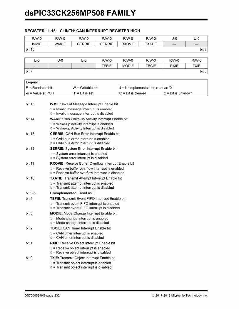
dsPIC33CK256MP508 FAMILY
REGISTER 11-15: C1INTH: CAN INTERRUPT REGISTER HIGH
R/W-0 R/W-0 R/W-0 R/W-0 R/W-0 R/W-0 U-0 U-0IVMIE WAKIE CERRIE SERRIE RXOVIE TXATIE — —
bit 15 bit 8
U-0 U-0 U-0 R/W-0 R/W-0 R/W-0 R/W-0 R/W-0— — — TEFIE MODIE TBCIE RXIE TXIE
bit 7 bit 0
Legend:R = Readable bit W = Writable bit U = Unimplemented bit, read as ‘0’-n = Value at POR ‘1’ = Bit is set ‘0’ = Bit is cleared x = Bit is unknown
bit 15 IVMIE: Invalid Message Interrupt Enable bit1 = Invalid message interrupt is enabled0 = Invalid message interrupt is disabled
bit 14 WAKIE: Bus Wake-up Activity Interrupt Enable bit1 = Wake-up activity interrupt is enabled0 = Wake-up Activity Interrupt is disabled
bit 13 CERRIE: CAN Bus Error Interrupt Enable bit1 = CAN bus error interrupt is enabled0 = CAN bus error interrupt is disabled
bit 12 SERRIE: System Error Interrupt Enable bit1 = System error interrupt is enabled0 = System error interrupt is disabled
bit 11 RXOVIE: Receive Buffer Overflow Interrupt Enable bit1 = Receive buffer overflow interrupt is enabled0 = Receive buffer overflow interrupt is disabled
bit 10 TXATIE: Transmit Attempt Interrupt Enable bit1 = Transmit attempt interrupt is enabled0 = Transmit attempt interrupt is disabled
bit 9-5 Unimplemented: Read as ‘0’bit 4 TEFIE: Transmit Event FIFO Interrupt Enable bit
1 = Transmit event FIFO interrupt is enabled0 = Transmit event FIFO interrupt is disabled
bit 3 MODIE: Mode Change Interrupt Enable bit1 = Mode change interrupt is enabled0 = Mode change interrupt is disabled
bit 2 TBCIE: CAN Timer Interrupt Enable bit1 = CAN timer interrupt is enabled0 = CAN timer interrupt is disabled
bit 1 RXIE: Receive Object Interrupt Enable bit1 = Receive object interrupt is enabled0 = Receive object interrupt is disabled
bit 0 TXIE: Transmit Object Interrupt Enable bit1 = Transmit object interrupt is enabled0 = Transmit object interrupt is disabled
DS70005349G-page 232 2017-2019 Microchip Technology Inc.

dsPIC33CK256MP508 FAMILY
REGISTER 11-16: C1INTL: CAN INTERRUPT REGISTER LOW
HS/C-0 HS/C-0 HS/C-0 HS/C-0 R-0 R-0 U-0 U-0IVMIF(1) WAKIF(1) CERRIF(1) SERRIF(1) RXOVIF TXATIF — —
bit 15 bit 8
U-0 U-0 U-0 R-0 HS/C-0 HS/C-0 R-0 R-0— — — TEFIF MODIF(1) TBCIF(1) RXIF TXIF
bit 7 bit 0
Legend: C = Clearable bit HS = Hardware Settable bitR = Readable bit W = Writable bit U = Unimplemented bit, read as ‘0’-n = Value at POR ‘1’ = Bit is set ‘0’ = Bit is cleared x = Bit is unknown
bit 15 IVMIF: Invalid Message Interrupt Flag bit(1)
1 = Invalid message interrupt occurred0 = No invalid message interrupt occurred
bit 14 WAKIF: Bus Wake-up Activity Interrupt Flag bit(1)
1 = Wake-up activity interrupt occurred0 = No wake-up activity interrupt occurred
bit 13 CERRIF: CAN Bus Error Interrupt Flag bit(1)
1 = CAN bus error interrupt occurred0 = No CAN bus error interrupt occurred
bit 12 SERRIF: System Error Interrupt Flag bit(1)
1 = System error interrupt occurred0 = No system error interrupt occurred
bit 11 RXOVIF: Receive Buffer Overflow Interrupt Flag bit1 = Receive buffer overflow interrupt occurred0 = No receive buffer overflow interrupt occurred
bit 10 TXATIF: Transmit Attempt Interrupt Flag bit1 = Transmit attempt interrupt occurred0 = No transmit attempt Interrupt occurred
bit 9-5 Unimplemented: Read as ‘0’bit 4 TEFIF: Transmit Event FIFO Interrupt Flag bit
1 = Transmit event FIFO interrupt occurred0 = No transmit event FIFO interrupt occurred
bit 3 MODIF: CAN Mode Change Interrupt Flag bit(1)
1 = CAN module mode change occurred (OPMOD[2:0] have changed to reflect REQOP[2:0])0 = No mode change occurred
bit 2 TBCIF: CAN Timer Overflow Interrupt Flag bit(1)
1 = TBC has overflowed0 = TBC has not overflowed
bit 1 RXIF: Receive Object Interrupt Flag bit1 = Receive object interrupt is pending0 = No receive object interrupts are pending
bit 0 TXIF: Transmit Object Interrupt Flag bit1 = Transmit object interrupt is pending0 = No transmit object interrupts are pending
Note 1: C1INTL: Flags are set by hardware and cleared by application.
2017-2019 Microchip Technology Inc. DS70005349G-page 233

dsPIC33CK256MP508 FAMILY
REGISTER 11-17: C1RXIFH: CAN RECEIVE INTERRUPT STATUS REGISTER HIGH(1)
R-0 R-0 R-0 R-0 R-0 R-0 R-0 R-0RFIF[31:24]
bit 15 bit 8
R-0 R-0 R-0 R-0 R-0 R-0 R-0 R-0RFIF[23:16]
bit 7 bit 0
Legend:R = Readable bit W = Writable bit U = Unimplemented bit, read as ‘0’-n = Value at POR ‘1’ = Bit is set ‘0’ = Bit is cleared x = Bit is unknown
bit 15-0 RFIF[31:16]: Unimplemented
Note 1: C1RXIFH: FIFO: RFIFx = ‘or’ of enabled RX FIFO flags (flags need to be cleared in the FIFO register).
REGISTER 11-18: C1RXIFL: CAN RECEIVE INTERRUPT STATUS REGISTER LOW(1)
R-0 R-0 R-0 R-0 R-0 R-0 R-0 R-0RFIF[15:8]
bit 15 bit 8
R-0 R-0 R-0 R-0 R-0 R-0 R-0 U-0RFIF[7:1] —
bit 7 bit 0
Legend:R = Readable bit W = Writable bit U = Unimplemented bit, read as ‘0’-n = Value at POR ‘1’ = Bit is set ‘0’ = Bit is cleared x = Bit is unknown
bit 15-8 RFIF[15:8]: Unimplementedbit 7-1 RFIF[7:1]: Receive FIFO Interrupt Pending bits
1 = One or more enabled receive FIFO interrupts are pending0 = No enabled receive FIFO interrupts are pending
bit 0 Unimplemented: Read as ‘0’
Note 1: C1RXIFL: FIFO: RFIFx = ‘or’ of enabled RX FIFO flags (flags need to be cleared in the FIFO register).
DS70005349G-page 234 2017-2019 Microchip Technology Inc.

dsPIC33CK256MP508 FAMILY
REGISTER 11-19: C1RXOVIFH: CAN RECEIVE OVERFLOW INTERRUPT STATUS REGISTER HIGH(1)
R-0 R-0 R-0 R-0 R-0 R-0 R-0 R-0RFOVIF[31:24]
bit 15 bit 8
R-0 R-0 R-0 R-0 R-0 R-0 R-0 R-0RFOVIF[23:16]
bit 7 bit 0
Legend:R = Readable bit W = Writable bit U = Unimplemented bit, read as ‘0’-n = Value at POR ‘1’ = Bit is set ‘0’ = Bit is cleared x = Bit is unknown
bit 15-0 RFOVIF[31:16]: Unimplemented
Note 1: C1RXOVIFH: FIFO: RFOVIFx (flag needs to be cleared in the FIFO register).
REGISTER 11-20: C1RXOVIFL: CAN RECEIVE OVERFLOW INTERRUPT STATUS REGISTER LOW(1)
R-0 R-0 R-0 R-0 R-0 R-0 R-0 R-0RFOVIF[15:8]
bit 15 bit 8
R-0 R-0 R-0 R-0 R-0 R-0 R-0 U-0RFOVIF[7:1] —
bit 7 bit 0
Legend:R = Readable bit W = Writable bit U = Unimplemented bit, read as ‘0’-n = Value at POR ‘1’ = Bit is set ‘0’ = Bit is cleared x = Bit is unknown
bit 15-8 RFOVIF[15:8]: Unimplementedbit 7-1 RFOVIF[7:1]: Receive FIFO Overflow Interrupt Pending bits
1 = Interrupt is pending0 = Interrupt is not pending
bit 0 Unimplemented: Read as ‘0’
Note 1: C1RXOVIFL: FIFO: RFOVIFx (flag needs to be cleared in the FIFO register).
2017-2019 Microchip Technology Inc. DS70005349G-page 235

dsPIC33CK256MP508 FAMILY
REGISTER 11-21: C1TXIFH: CAN TRANSMIT INTERRUPT STATUS REGISTER HIGH(1)
R-0 R-0 R-0 R-0 R-0 R-0 R-0 R-0TFIF[31:24]
bit 15 bit 8
R-0 R-0 R-0 R-0 R-0 R-0 R-0 R-0TFIF[23:16]
bit 7 bit 0
Legend:R = Readable bit W = Writable bit U = Unimplemented bit, read as ‘0’-n = Value at POR ‘1’ = Bit is set ‘0’ = Bit is cleared x = Bit is unknown
bit 15-0 TFIF[31:16]: Unimplemented
Note 1: C1TXIFH: FIFO: TFIFx = ‘or’ of the enabled TX FIFO flags (flags need to be cleared in the FIFO register).
REGISTER 11-22: C1TXIFL: CAN TRANSMIT INTERRUPT STATUS REGISTER LOW(1)
R-0 R-0 R-0 R-0 R-0 R-0 R-0 R-0TFIF[15:8]
bit 15 bit 8
R-0 R-0 R-0 R-0 R-0 R-0 R-0 R-0TFIF[7:0](2)
bit 7 bit 0
Legend:R = Readable bit W = Writable bit U = Unimplemented bit, read as ‘0’-n = Value at POR ‘1’ = Bit is set ‘0’ = Bit is cleared x = Bit is unknown
bit 15-8 TFIF[15:8]: Unimplementedbit 7-0 TFIF[7:0]: Transmit FIFO/TXQ Interrupt Pending bits(2)
1 = One or more enabled transmit FIFO/TXQ interrupts are pending0 = No enabled transmit FIFO/TXQ interrupts are pending
Note 1: C1TXIFL: FIFO: TFIFx = ‘or’ of the enabled TX FIFO flags (flags need to be cleared in the FIFO register).2: TFIF0 is for the transmit queue.
DS70005349G-page 236 2017-2019 Microchip Technology Inc.

dsPIC33CK256MP508 FAMILY
REGISTER 11-23: C1TXATIFH: CAN TRANSMIT ATTEMPT INTERRUPT STATUS REGISTER HIGH(1)
R-0 R-0 R-0 R-0 R-0 R-0 R-0 R-0TFATIF[31:24]
bit 15 bit 8
R-0 R-0 R-0 R-0 R-0 R-0 R-0 R-0TFATIF[23:16]
bit 7 bit 0
Legend:R = Readable bit W = Writable bit U = Unimplemented bit, read as ‘0’-n = Value at POR ‘1’ = Bit is set ‘0’ = Bit is cleared x = Bit is unknown
bit 15-0 TFATIF[31:16]: Unimplemented
Note 1: C1TXATIFH: FIFO: TFATIFx (flag needs to be cleared in the FIFO register).
REGISTER 11-24: C1TXATIFL: CAN TRANSMIT ATTEMPT INTERRUPT STATUS REGISTER LOW(1)
R-0 R-0 R-0 R-0 R-0 R-0 R-0 R-0TFATIF[15:8]
bit 15 bit 8
R-0 R-0 R-0 R-0 R-0 R-0 R-0 R-0TFATIF[7:0](2)
bit 7 bit 0
Legend:R = Readable bit W = Writable bit U = Unimplemented bit, read as ‘0’-n = Value at POR ‘1’ = Bit is set ‘0’ = Bit is cleared x = Bit is unknown
bit 15-8 TFATIF[15:8]: Unimplementedbit 7-0 TFATIF[7:0]: Transmit FIFO/TXQ Attempt Interrupt Pending bits(2)
1 = Interrupt is pending0 = Interrupt is not pending
Note 1: C1TXATIFL: FIFO: TFATIFx (flag needs to be cleared in the FIFO register).2: TFATIF0 is for the transmit queue.
2017-2019 Microchip Technology Inc. DS70005349G-page 237

dsPIC33CK256MP508 FAMILY
REGISTER 11-25: C1TXREQH: CAN TRANSMIT REQUEST REGISTER HIGH
S/HC-0 S/HC-0 S/HC-0 S/HC-0 S/HC-0 S/HC-0 S/HC-0 S/HC-0TXREQ[31:24]
bit 15 bit 8
S/HC-0 S/HC-0 S/HC-0 S/HC-0 S/HC-0 S/HC-0 S/HC-0 S/HC-0TXREQ[23:16]
bit 7 bit 0
Legend: S = Settable bit HC = Hardware Clearable bitR = Readable bit W = Writable bit U = Unimplemented bit, read as ‘0’-n = Value at POR ‘1’ = Bit is set ‘0’ = Bit is cleared x = Bit is unknown
bit 15-0 TXREQ[31:16]: Unimplemented
REGISTER 11-26: C1TXREQL: CAN TRANSMIT REQUEST REGISTER LOW
S/HC-0 S/HC-0 S/HC-0 S/HC-0 S/HC-0 S/HC-0 S/HC-0 S/HC-0TXREQ[15:8]
bit 15 bit 8
S/HC-0 S/HC-0 S/HC-0 S/HC-0 S/HC-0 S/HC-0 S/HC-0 S/HC-0TXREQ[7:1] TXREQ0
bit 7 bit 0
Legend: S = Settable bit HC = Hardware Clearable bitR = Readable bit W = Writable bit U = Unimplemented bit, read as ‘0’-n = Value at POR ‘1’ = Bit is set ‘0’ = Bit is cleared x = Bit is unknown
bit 15-8 TXREQ[15:8]: Unimplementedbit 7-1 TXREQ[7:1]: Message Send Request bits
TXEN = 1 (object configured as a transmit object):Setting this bit to ‘1’ requests sending a message. The bit will automatically clear when the message(s)queued in the object is (are) successfully sent. This bit can NOT be used for aborting a transmission.TXEN = 0 (object configured as a receive object):This bit has no effect.
bit 0 TXREQ0: Transmit Queue Message Send Request bitSetting this bit to ‘1’ requests sending a message. The bit will automatically clear when the message(s)queued in the object is (are) successfully sent. This bit can NOT be used for aborting a transmission.
DS70005349G-page 238 2017-2019 Microchip Technology Inc.

dsPIC33CK256MP508 FAMILY
REGISTER 11-27: C1FIFOBAH: CAN MESSAGE MEMORY BASE ADDRESS REGISTER HIGH
R/W-0 R/W-0 R/W-0 R/W-0 R/W-0 R/W-0 R/W-0 R/W-0FIFOBA[31:24]
bit 15 bit 8
R/W-0 R/W-0 R/W-0 R/W-0 R/W-0 R/W-0 R/W-0 R/W-0FIFOBA[23:16]
bit 7 bit 0
Legend:R = Readable bit W = Writable bit U = Unimplemented bit, read as ‘0’-n = Value at POR ‘1’ = Bit is set ‘0’ = Bit is cleared x = Bit is unknown
bit 15-0 FIFOBA[31:16]: Message Memory Base Address bitsDefines the base address for the transmit event FIFO followed by the message objects.
REGISTER 11-28: C1FIFOBAL: CAN MESSAGE MEMORY BASE ADDRESS REGISTER LOW
R/W-0 R/W-0 R/W-0 R/W-0 R/W-0 R/W-0 R/W-0 R/W-0FIFOBA[15:8]
bit 15 bit 8
R/W-0 R/W-0 R/W-0 R/W-0 R/W-0 R/W-0 R-0(1) R-0(1)
FIFOBA[7:0]bit 7 bit 0
Legend:R = Readable bit W = Writable bit U = Unimplemented bit, read as ‘0’-n = Value at POR ‘1’ = Bit is set ‘0’ = Bit is cleared x = Bit is unknown
bit 15-0 FIFOBA[15:0]: Message Memory Base Address bits(1)
Defines the base address for the transmit event FIFO followed by the message objects.
Note 1: Bits[1:0] are ‘0’ to make base address location 32-bit word-aligned.
2017-2019 Microchip Technology Inc. DS70005349G-page 239

dsPIC33CK256MP508 FAMILY
REGISTER 11-29: C1TXQCONH: CAN TRANSMIT QUEUE CONTROL REGISTER HIGH
R/W-0 R/W-0 R/W-0 R/W-0 R/W-0 R/W-0 R/W-0 R/W-0PLSIZE2(1) PLSIZE1(1) PLSIZE0(1) FSIZE4(1) FSIZE3(1) FSIZE2(1) FSIZE1(1) FSIZE0(1)
bit 15 bit 8
U-0 R/W-1 R/W-1 R/W-0 R/W-0 R/W-0 R/W-0 R/W-0— TXAT1 TXAT0 TXPRI4 TXPRI3 TXPRI2 TXPRI1 TXPRI0
bit 7 bit 0
Legend:R = Readable bit W = Writable bit U = Unimplemented bit, read as ‘0’-n = Value at POR ‘1’ = Bit is set ‘0’ = Bit is cleared x = Bit is unknown
bit 15-13 PLSIZE[2:0]: Payload Size bits(1)
111 = 64 data bytes110 = 48 data bytes101 = 32 data bytes100 = 24 data bytes011 = 20 data bytes010 = 16 data bytes001 = 12 data bytes000 = 8 data bytes
bit 12-8 FSIZE[4:0]: FIFO Size bits(1)
11111 = FIFO is 32 messages deep...00010 = FIFO is 3 messages deep00001 = FIFO is 2 messages deep00000 = FIFO is 1 message deep
bit 7 Unimplemented: Read as ‘0’bit 6-5 TXAT[1:0]: Retransmission Attempts bits
This feature is enabled when RTXAT (C1CONH[0]) is set.11 = Unlimited number of retransmission attempts10 = Unlimited number of retransmission attempts01 = Three retransmission attempts00 = Disables retransmission attempts
bit 4-0 TXPRI[4:0]: Message Transmit Priority bits11111 = Highest message priority...00000 = Lowest message priority
Note 1: These bits can only be modified in Configuration mode (OPMOD[2:0] = 100).
DS70005349G-page 240 2017-2019 Microchip Technology Inc.

dsPIC33CK256MP508 FAMILY
REGISTER 11-30: C1TXQCONL: CAN TRANSMIT QUEUE CONTROL REGISTER LOW
U-0 U-0 U-0 U-0 U-0 R/W-0 R/W-0 R/W-0— — — — — FRESET TXREQ UINC
bit 15 bit 8
R-0 U-0 U-0 R/W-0 U-0 R/W-0 U-0 R/W-0TXEN — — TXATIE — TXQEIE — TXQNIE
bit 7 bit 0
Legend:R = Readable bit W = Writable bit U = Unimplemented bit, read as ‘0’-n = Value at POR ‘1’ = Bit is set ‘0’ = Bit is cleared x = Bit is unknown
bit 15-11 Unimplemented: Read as ‘0’bit 10 FRESET: FIFO Reset bit
1 = FIFO will be reset when bit is set, cleared by hardware when FIFO is reset; user should pollwhether this bit is clear before taking any action
0 = No effectbit 9 TXREQ: Message Send Request bit
1 = Requests sending a message; the bit will automatically clear when all the messages queued inthe TXQ are successfully sent
0 = Clearing the bit to ‘0’ while set (‘1’) will request a message abortbit 8 UINC: Increment Head/Tail bit
When this bit is set, the FIFO head will increment by a single message.bit 7 TXEN: TX Enable bitbit 6-5 Unimplemented: Read as ‘0’bit 4 TXATIE: Transmit Attempts Exhausted Interrupt Enable bit
1 = Enables interrupt0 = Disables interrupt
bit 3 Unimplemented: Read as ‘0’bit 2 TXQEIE: Transmit Queue Empty Interrupt Enable bit
1 = Interrupt is enabled for TXQ empty0 = Interrupt is disabled for TXQ empty
bit 1 Unimplemented: Read as ‘0’bit 0 TXQNIE: Transmit Queue Not Full Interrupt Enable bit
1 = Interrupt is enabled for TXQ not full0 = Interrupt is disabled for TXQ not full
2017-2019 Microchip Technology Inc. DS70005349G-page 241

dsPIC33CK256MP508 FAMILY
REGISTER 11-31: C1TXQSTA: CAN TRANSMIT QUEUE STATUS REGISTER
U-0 U-0 U-0 R-0 R-0 R-0 R-0 R-0— — — TXQCI[4:0](1)
bit 15 bit 8
R-0 R-0 R-0 C/HS-0 U-0 R-1 U-0 R-1TXABT(2) TXLARB TXERR TXATIF — TXQEIF — TXQNIF
bit 7 bit 0
Legend: C = Clearable bit HS = Hardware Settable bitR = Readable bit W = Writable bit U = Unimplemented bit, read as ‘0’-n = Value at POR ‘1’ = Bit is set ‘0’ = Bit is cleared x = Bit is unknown
bit 15-13 Unimplemented: Read as ‘0’bit 12-8 TXQCI[4:0]: Transmit Message Queue Index bits(1)
A read of this register will return an index to the message that the FIFO will next attempt to transmit.bit 7 TXABT: Message Aborted Status bit(2)
1 = Message was aborted0 = Message completed successfully
bit 6 TXLARB: Message Lost Arbitration Status bit1 = Message lost arbitration while being sent0 = Message did not lose arbitration while being sent
bit 5 TXERR: Error Detected During Transmission bit1 = A bus error occurred while the message was being sent0 = A bus error did not occur while the message was being sent
bit 4 TXATIF: Transmit Attempts Exhausted Interrupt Pending bit1 = Interrupt is pending0 = Interrupt is not pending
bit 3 Unimplemented: Read as ‘0’bit 2 TXQEIF: Transmit Queue Empty Interrupt Flag bit
1 = TXQ is empty0 = TXQ is not empty, at least 1 message is queued to be transmitted
bit 1 Unimplemented: Read as ‘0’bit 0 TXQNIF: Transmit Queue Not Full Interrupt Flag bit
1 = TXQ is not full0 = TXQ is full
Note 1: The TXQCI[4:0] bits give a zero-indexed value to the message in the TXQ. If the TXQ is four messages deep (FSIZE[4:0] = 3), TXQCIx will take on a value of 0 to 3, depending on the state of the TXQ.
2: This bit is updated when a message completes (or aborts) or when the TXQ is reset.
DS70005349G-page 242 2017-2019 Microchip Technology Inc.

dsPIC33CK256MP508 FAMILY
REGISTER 11-32: C1FIFOCONHx: CAN FIFO CONTROL REGISTER x (x = 1 TO 7) HIGH
R/W-0 R/W-0 R/W-0 R/W-0 R/W-0 R/W-0 R/W-0 R/W-0PLSIZE2(1) PLSIZE1(1) PLSIZE0(1) FSIZE4(1) FSIZE3(1) FSIZE2(1) FSIZE1(1) FSIZE0(1)
bit 15 bit 8
U-0 R/W-1 R/W-1 R/W-0 R/W-0 R/W-0 R/W-0 R/W-0— TXAT1 TXAT0 TXPRI4 TXPRI3 TXPRI2 TXPRI1 TXPRI0
bit 7 bit 0
Legend:R = Readable bit W = Writable bit U = Unimplemented bit, read as ‘0’-n = Value at POR ‘1’ = Bit is set ‘0’ = Bit is cleared x = Bit is unknown
bit 15-13 PLSIZE[2:0]: Payload Size bits(1)
111 = 64 data bytes110 = 48 data bytes101 = 32 data bytes100 = 24 data bytes011 = 20 data bytes010 = 16 data bytes001 = 12 data bytes000 = 8 data bytes
bit 12-8 FSIZE[4:0]: FIFO Size bits(1)
11111 = FIFO is 32 messages deep...00010 = FIFO is 3 messages deep00001 = FIFO is 2 messages deep00000 = FIFO is 1 message deep
bit 7 Unimplemented: Read as ‘0’bit 6-5 TXAT[1:0]: Retransmission Attempts bits
This feature is enabled when RTXAT (C1CONH[0]) is set.11 = Unlimited number of retransmission attempts10 = Unlimited number of retransmission attempts01 = Three retransmission attempts00 = Disables retransmission attempts
bit 4-0 TXPRI[4:0]: Message Transmit Priority bits11111 = Highest message priority...00000 = Lowest message priority
Note 1: These bits can only be modified in Configuration mode (OPMOD[2:0] = 100).
2017-2019 Microchip Technology Inc. DS70005349G-page 243

dsPIC33CK256MP508 FAMILY
REGISTER 11-33: C1FIFOCONLx: CAN FIFO CONTROL REGISTER x (x = 1 TO 7) LOW
U-0 U-0 U-0 U-0 U-0 S/HC-1 R/W/HC-0 S/HC-0— — — — — FRESET TXREQ UINC
bit 15 bit 8
R/W-0 R/W-0 R/W-0 R/W-0 R/W-0 R/W-0 R/W-0 R/W-0TXEN RTREN RXTSEN(1) TXATIE RXOVIE TFERFFIE TFHRFHIE TFNRFNIE
bit 7 bit 0
Legend: S = Settable bit HC = Hardware Clearable bitR = Readable bit W = Writable bit U = Unimplemented bit, read as ‘0’-n = Value at POR ‘1’ = Bit is set ‘0’ = Bit is cleared x = Bit is unknown
bit 15-11 Unimplemented: Read as ‘0’bit 10 FRESET: FIFO Reset bit
1 = FIFO will be reset when bit is set, cleared by hardware when FIFO is reset; user should pollwhether this bit is clear before taking any action
0 = No effectbit 9 TXREQ: Message Send Request bit
TXEN = 1 (FIFO configured as a transmit FIFO):1 = Requests sending a message; the bit will automatically clear when all the messages queued in
the FIFO are successfully sent0 = Clearing the bit to ‘0’ while set (‘1’) will request a message abortTXEN = 0 (FIFO configured as a receive FIFO):This bit has no effect.
bit 8 UINC: Increment Head/Tail bitTXEN = 1 (FIFO configured as a transmit FIFO):When this bit is set, the FIFO head will increment by a single message.TXEN = 0 (FIFO configured as a receive FIFO):When this bit is set, the FIFO tail will increment by a single message.
bit 7 TXEN: TX/RX Buffer Selection bit1 = Transmits message object0 = Receives message object
bit 6 RTREN: Auto-Remote Transmit (RTR) Enable bit1 = When a Remote Transmit is received, TXREQ will be set0 = When a Remote Transmit is received, TXREQ will be unaffected
bit 5 RXTSEN: Received Message Timestamp Enable bit(1)
1 = Captures timestamp in received message object in RAM0 = Does not capture timestamp
bit 4 TXATIE: Transmit Attempts Exhausted Interrupt Enable bit1 = Enables interrupt0 = Disables interrupt
bit 3 RXOVIE: Overflow Interrupt Enable bit1 = Interrupt is enabled for overflow event0 = Interrupt is disabled for overflow event
Note 1: This bit can only be modified in Configuration mode (OPMOD[2:0] = 100).
DS70005349G-page 244 2017-2019 Microchip Technology Inc.

dsPIC33CK256MP508 FAMILY
bit 2 TFERFFIE: Transmit/Receive FIFO Empty/Full Interrupt Enable bitTXEN = 1 (FIFO configured as a transmit FIFO):Transmit FIFO Empty Interrupt Enable1 = Interrupt is enabled for FIFO empty0 = Interrupt is disabled for FIFO emptyTXEN = 0 (FIFO configured as a receive FIFO):Receive FIFO Full Interrupt Enable1 = Interrupt is enabled for FIFO full0 = Interrupt is disabled for FIFO full
bit 1 TFHRFHIE: Transmit/Receive FIFO Half Empty/Half Full Interrupt Enable bitTXEN = 1 (FIFO configured as a transmit FIFO):Transmit FIFO Half Empty Interrupt Enable1 = Interrupt is enabled for FIFO half empty0 = Interrupt is disabled for FIFO half emptyTXEN = 0 (FIFO configured as a receive FIFO):Receive FIFO Half Full Interrupt Enable1 = Interrupt is enabled for FIFO half full0 = Interrupt is disabled for FIFO half full
bit 0 TFNRFNIE: Transmit/Receive FIFO Not Full/Not Empty Interrupt Enable bitTXEN = 1 (FIFO configured as a transmit FIFO):Transmit FIFO Not Full Interrupt Enable1 = Interrupt is enabled for FIFO not full0 = Interrupt is disabled for FIFO not fullTXEN = 0 (FIFO configured as a receive FIFO):Receive FIFO Not Empty Interrupt Enable1 = Interrupt is enabled for FIFO not empty0 = Interrupt is disabled for FIFO not empty
REGISTER 11-33: C1FIFOCONLx: CAN FIFO CONTROL REGISTER x (x = 1 TO 7) LOW (CONTINUED)
Note 1: This bit can only be modified in Configuration mode (OPMOD[2:0] = 100).
2017-2019 Microchip Technology Inc. DS70005349G-page 245

dsPIC33CK256MP508 FAMILY
REGISTER 11-34: C1FIFOSTAx: CAN FIFO STATUS REGISTER x (x = 1 TO 7)
U-0 U-0 U-0 R-0 R-0 R-0 R-0 R-0— — — FIFOCI[4:0](1)
bit 15 bit 8
R-0 R-0 R-0 C/HS-0 C/HS-0 R-0 R-0 R-0TXABT(3) TXLARB(2) TXERR(2) TXATIF RXOVIF TFERFFIF TFHRFHIF TFNRFNIF
bit 7 bit 0
Legend: C = Clearable bit HS = Hardware Settable bitR = Readable bit W = Writable bit U = Unimplemented bit, read as ‘0’-n = Value at POR ‘1’ = Bit is set ‘0’ = Bit is cleared x = Bit is unknown
bit 15-13 Unimplemented: Read as ‘0’bit 12-8 FIFOCI[4:0]: FIFO Message Index bits(1)
TXEN = 1 (FIFO configured as a transmit buffer):A read of this register will return an index to the message that the FIFO will next attempt to transmit.TXEN = 0 (FIFO configured as a receive buffer):A read of this register will return an index to the message that the FIFO will use to save the nextmessage.
bit 7 TXABT: Message Aborted Status bit(3)
1 = Message was aborted0 = Message completed successfully
bit 6 TXLARB: Message Lost Arbitration Status bit(2)
1 = Message lost arbitration while being sent0 = Message did not lose arbitration while being sent
bit 5 TXERR: Error Detected During Transmission bit(2)
1 = A bus error occurred while the message was being sent0 = A bus error did not occur while the message was being sent
bit 4 TXATIF: Transmit Attempts Exhausted Interrupt Pending bitTXEN = 1 (FIFO configured as a transmit buffer):1 = Interrupt is pending0 = Interrupt is not pendingTXEN = 0 (FIFO configured as a receive buffer):Unused, read as ‘0’.
bit 3 RXOVIF: Receive FIFO Overflow Interrupt Flag bitTXEN = 1 (FIFO configured as a transmit buffer):Unused, read as ‘0’.TXEN = 0 (FIFO configured as a receive buffer):1 = Overflow event has occurred0 = No overflow event has occurred
Note 1: FIFOCI[4:0] gives a zero-indexed value to the message in the FIFO. If the FIFO is four messages deep (FSIZE[4:0] = 3), FIFOCIx will take on a value of 0 to 3, depending on the state of the FIFO.
2: These bits are updated when a message completes (or aborts) or when the FIFO is reset.3: This bit is reset on any read of this register or when the TXQ is reset. The bits are cleared when TXREQ is
set or using an SPI write.
DS70005349G-page 246 2017-2019 Microchip Technology Inc.

dsPIC33CK256MP508 FAMILY
bit 2 TFERFFIF: Transmit/Receive FIFO Empty/Full Interrupt Flag bitTXEN = 1 (FIFO configured as a transmit FIFO):Transmit FIFO Empty Interrupt Flag1 = FIFO is empty0 = FIFO is not empty, at least 1 message is queued to be transmittedTXEN = 0 (FIFO configured as a receive FIFO):Receive FIFO Full Interrupt Flag1 = FIFO is full0 = FIFO is not full
bit 1 TFHRFHIF: Transmit/Receive FIFO Half Empty/Half Full Interrupt Flag bitTXEN = 1 (FIFO configured as a transmit FIFO):Transmit FIFO Half Empty Interrupt Flag1 = FIFO is half full0 = FIFO is > half fullTXEN = 0 (FIFO configured as a receive FIFO):Receive FIFO Half Full Interrupt Flag1 = FIFO is half full0 = FIFO is < half full
bit 0 TFNRFNIF: Transmit/Receive FIFO Not Full/Not Empty Interrupt Flag bitTXEN = 1 (FIFO configured as a transmit FIFO):Transmit FIFO Not Full Interrupt Flag1 = FIFO is not full0 = FIFO is fullTXEN = 0 (FIFO configured as a receive FIFO):Receive FIFO Not Empty Interrupt Flag1 = FIFO is not empty, has at least 1 message0 = FIFO is empty
REGISTER 11-34: C1FIFOSTAx: CAN FIFO STATUS REGISTER x (x = 1 TO 7) (CONTINUED)
Note 1: FIFOCI[4:0] gives a zero-indexed value to the message in the FIFO. If the FIFO is four messages deep (FSIZE[4:0] = 3), FIFOCIx will take on a value of 0 to 3, depending on the state of the FIFO.
2: These bits are updated when a message completes (or aborts) or when the FIFO is reset.3: This bit is reset on any read of this register or when the TXQ is reset. The bits are cleared when TXREQ is
set or using an SPI write.
2017-2019 Microchip Technology Inc. DS70005349G-page 247

dsPIC33CK256MP508 FAMILY
REGISTER 11-35: C1TEFCONH: CAN TRANSMIT EVENT FIFO CONTROL REGISTER HIGH
U-0 U-0 U-0 R/W-0 R/W-0 R/W-0 R/W-0 R/W-0— — — FSIZE[4:0](1)
bit 15 bit 8
U-0 U-0 U-0 U-0 U-0 U-0 U-0 U-0— — — — — — — —
bit 7 bit 0
Legend:R = Readable bit W = Writable bit U = Unimplemented bit, read as ‘0’-n = Value at POR ‘1’ = Bit is set ‘0’ = Bit is cleared x = Bit is unknown
bit 15-13 Unimplemented: Read as ‘0’bit 12-8 FSIZE[4:0]: FIFO Size bits(1)
11111 = FIFO is 32 messages deep...00010 = FIFO is 3 messages deep00001 = FIFO is 2 messages deep00000 = FIFO is 1 message deep
bit 7-0 Unimplemented: Read as ‘0’
Note 1: These bits can only be modified in Configuration mode (OPMOD[2:0] = 100).
DS70005349G-page 248 2017-2019 Microchip Technology Inc.

dsPIC33CK256MP508 FAMILY
REGISTER 11-36: C1TEFCONL: CAN TRANSMIT EVENT FIFO CONTROL REGISTER LOW
U-0 U-0 U-0 U-0 U-0 S/HC-0 U-0 S/HC-0— — — — — FRESET — UINC
bit 15 bit 8
U-0 U-0 R/W-0 U-0 R/W-0 R/W-0 R/W-0 R/W-0— — TEFTSEN(1) — TEFOVIE TEFFIE TEFHIE TEFNEIE
bit 7 bit 0
Legend: S = Settable bit HC = Hardware Clearable bitR = Readable bit W = Writable bit U = Unimplemented bit, read as ‘0’-n = Value at POR ‘1’ = Bit is set ‘0’ = Bit is cleared x = Bit is unknown
bit 15-11 Unimplemented: Read as ‘0’bit 10 FRESET: FIFO Reset bit
1 = FIFO will be reset when bit is set, cleared by hardware when FIFO is reset; the user should pollwhether this bit is clear before taking any action
0 = No effectbit 9 Unimplemented: Read as ‘0’bit 8 UINC: Increment Tail bit
1 = When this bit is set, the FIFO tail will increment by a single message0 = FIFO tail will not increment
bit 7-6 Unimplemented: Read as ‘0’bit 5 TEFTSEN: Transmit Event FIFO Timestamp Enable bit(1)
1 = Timestamps elements in TEF0 = Does not timestamp elements in TEF
bit 4 Unimplemented: Read as ‘0’bit 3 TEFOVIE: Transmit Event FIFO Overflow Interrupt Enable bit
1 = Interrupt is enabled for overflow event0 = Interrupt is disabled for overflow event
bit 2 TEFFIE: Transmit Event FIFO Full Interrupt Enable bit1 = Interrupt is enabled for FIFO full0 = Interrupt is disabled for FIFO full
bit 1 TEFHIE: Transmit Event FIFO Half Full Interrupt Enable bit1 = Interrupt is enabled for FIFO half full0 = Interrupt is disabled for FIFO half full
bit 0 TEFNEIE: Transmit Event FIFO Not Empty Interrupt Enable bit1 = Interrupt is enabled for FIFO not empty0 = Interrupt is disabled for FIFO not empty
Note 1: These bits can only be modified in Configuration mode (OPMOD[2:0] = 100).
2017-2019 Microchip Technology Inc. DS70005349G-page 249

dsPIC33CK256MP508 FAMILY
REGISTER 11-37: C1TEFSTA: CAN TRANSMIT EVENT FIFO STATUS REGISTER
U-0 U-0 U-0 U-0 U-0 U-0 U-0 U-0— — — — — — — —
bit 15 bit 8
U-0 U-0 U-0 U-0 S/HC-0 R-0 R-0 R-0— — — — TEFOVIF TEFFIF(1) TEFHIF(1) TEFNEIF(1)
bit 7 bit 0
Legend: HC = Hardware Clearable bit S = Settable bit Can Set by ‘1’R = Readable bit W = Writable bit U = Unimplemented bit, read as ‘0’-n = Value at POR ‘1’ = Bit is set ‘0’ = Bit is cleared x = Bit is unknown
bit 15-4 Unimplemented: Read as ‘0’bit 3 TEFOVIF: Transmit Event FIFO Overflow Interrupt Flag bit
1 = Overflow event has occurred0 = No overflow event has occurred
bit 2 TEFFIF: Transmit Event FIFO Full Interrupt Flag bit(1)
1 = FIFO is full0 = FIFO is not full
bit 1 TEFHIF: Transmit Event FIFO Half Full Interrupt Flag bit(1)
1 = FIFO is half full0 = FIFO is < half full
bit 0 TEFNEIF: Transmit Event FIFO Not Empty Interrupt Flag bit(1)
1 = FIFO is not empty0 = FIFO is empty
Note 1: These bits are read-only and reflect the status of the FIFO.
DS70005349G-page 250 2017-2019 Microchip Technology Inc.

dsPIC33CK256MP508 FAMILY
REGISTER 11-38: C1FIFOUAHx: CAN FIFO USER ADDRESS REGISTER x (x = 1 TO 7) HIGH(1)
R-x R-x R-x R-x R-x R-x R-x R-xFIFOUA[31:24]
bit 15 bit 8
R-x R-x R-x R-x R-x R-x R-x R-xFIFOUA[23:16]
bit 7 bit 0
Legend:R = Readable bit W = Writable bit U = Unimplemented bit, read as ‘0’-n = Value at POR ‘1’ = Bit is set ‘0’ = Bit is cleared x = Bit is unknown
bit 15-0 FIFOUA[31:16]: FIFO User Address bitsTXEN = 1 (FIFO configured as a transmit buffer):A read of this register will return the address where the next message is to be written (FIFO head).TXEN = 0 (FIFO configured as a receive buffer):A read of this register will return the address where the next message is to be read (FIFO tail).
Note 1: This register is not ensured to read correctly in Configuration mode and should only be accessed when the module is not in Configuration mode.
REGISTER 11-39: C1FIFOUALx: CAN FIFO USER ADDRESS REGISTER x (x = 1 TO 7) LOW(1)
R-x R-x R-x R-x R-x R-x R-x R-xFIFOUA[15:8]
bit 15 bit 8
R-x R-x R-x R-x R-x R-x R-x R-xFIFOUA[7:0]
bit 7 bit 0
Legend:R = Readable bit W = Writable bit U = Unimplemented bit, read as ‘0’-n = Value at POR ‘1’ = Bit is set ‘0’ = Bit is cleared x = Bit is unknown
bit 15-0 FIFOUA[15:0]: FIFO User Address bitsTXEN = 1 (FIFO configured as a transmit buffer):A read of this register will return the address where the next message is to be written (FIFO head).TXEN = 0 (FIFO configured as a receive buffer):A read of this register will return the address where the next message is to be read (FIFO tail).
Note 1: This register is not ensured to read correctly in Configuration mode and should only be accessed when the module is not in Configuration mode.
2017-2019 Microchip Technology Inc. DS70005349G-page 251

dsPIC33CK256MP508 FAMILY
REGISTER 11-40: C1TEFUAH: CAN TRANSMIT EVENT FIFO USER ADDRESS REGISTER HIGH(1)
R-x R-x R-x R-x R-x R-x R-x R-xTEFUA[31:24]
bit 15 bit 8
R-x R-x R-x R-x R-x R-x R-x R-xTEFUA[23:16]
bit 7 bit 0
Legend:R = Readable bit W = Writable bit U = Unimplemented bit, read as ‘0’-n = Value at POR ‘1’ = Bit is set ‘0’ = Bit is cleared x = Bit is unknown
bit 15-0 TEFUA[31:16]: Transmit Event FIFO User Address bitsA read of this register will return the address where the next event is to be read (FIFO tail).
Note 1: This register is not ensured to read correctly in Configuration mode and should only be accessed when the module is not in Configuration mode.
REGISTER 11-41: C1TEFUAL: CAN TRANSMIT EVENT FIFO USER ADDRESS REGISTER LOW(1)
R-x R-x R-x R-x R-x R-x R-x R-xTEFUA[15:8]
bit 15 bit 8
R-x R-x R-x R-x R-x R-x R-x R-xTEFUA[7:0]
bit 7 bit 0
Legend:R = Readable bit W = Writable bit U = Unimplemented bit, read as ‘0’-n = Value at POR ‘1’ = Bit is set ‘0’ = Bit is cleared x = Bit is unknown
bit 15-0 TEFUA[15:0]: Transmit Event FIFO User Address bitsA read of this register will return the address where the next event is to be read (FIFO tail).
Note 1: This register is not ensured to read correctly in Configuration mode and should only be accessed when the module is not in Configuration mode.
DS70005349G-page 252 2017-2019 Microchip Technology Inc.

dsPIC33CK256MP508 FAMILY
REGISTER 11-42: C1TXQUAH: CAN TRANSMIT QUEUE USER ADDRESS REGISTER HIGH(1)
R-x R-x R-x R-x R-x R-x R-x R-xTXQUA[31:24]
bit 15 bit 8
R-x R-x R-x R-x R-x R-x R-x R-xTXQUA[23:16]
bit 7 bit 0
Legend:R = Readable bit W = Writable bit U = Unimplemented bit, read as ‘0’-n = Value at POR ‘1’ = Bit is set ‘0’ = Bit is cleared x = Bit is unknown
bit 15-0 TXQUA[31:16]: TXQ User Address bitsA read of this register will return the address where the next message is to be written (TXQ head).
Note 1: This register is not ensured to read correctly in Configuration mode and should only be accessed when the module is not in Configuration mode.
REGISTER 11-43: C1TXQUAL: CAN TRANSMIT QUEUE USER ADDRESS REGISTER LOW(1)
R-x R-x R-x R-x R-x R-x R-x R-xTXQUA[15:8]
bit 15 bit 8
R-x R-x R-x R-x R-x R-x R-x R-xTXQUA[7:0]
bit 7 bit 0
Legend:R = Readable bit W = Writable bit U = Unimplemented bit, read as ‘0’-n = Value at POR ‘1’ = Bit is set ‘0’ = Bit is cleared x = Bit is unknown
bit 15-0 TXQUA[15:0]: TXQ User Address bitsA read of this register will return the address where the next message is to be written (TXQ head).
Note 1: This register is not ensured to read correctly in Configuration mode and should only be accessed when the module is not in Configuration mode.
2017-2019 Microchip Technology Inc. DS70005349G-page 253

dsPIC33CK256MP508 FAMILY
REGISTER 11-44: C1TRECH: CAN TRANSMIT/RECEIVE ERROR COUNT REGISTER HIGH
U-0 U-0 U-0 U-0 U-0 U-0 U-0 U-0— — — — — — — —
bit 15 bit 8
U-0 U-0 R-1 R-0 R-0 R-0 R-0 R-0— — TXBO TXBP RXBP TXWARN RXWARN EWARN
bit 7 bit 0
Legend:R = Readable bit W = Writable bit U = Unimplemented bit, read as ‘0’-n = Value at POR ‘1’ = Bit is set ‘0’ = Bit is cleared x = Bit is unknown
bit 15-6 Unimplemented: Read as ‘0’bit 5 TXBO: Transmitter in Bus Off Error State bit (TERRCNT[7:0] > 255)
In Configuration mode, TXBO is set since the module is not on the bus.bit 4 TXBP: Transmitter in Bus Passive Error State bit (TERRCNT[7:0] > 127)bit 3 RXBP: Receiver in Bus Passive Error State bit (RERRCNT[7:0] > 127)bit 2 TXWARN: Transmitter in Warning State bit (128 > TERRCNT[7:0] > 95)bit 1 RXWARN: Receiver in Warning State bit (128 > RERRCNT[7:0] > 95)bit 0 EWARN: Transmitter or Receiver in Warning State bit
REGISTER 11-45: C1TRECL: CAN TRANSMIT/RECEIVE ERROR COUNT REGISTER LOW
R-0 R-0 R-0 R-0 R-0 R-0 R-0 R-0TERRCNT[7:0]
bit 15 bit 8
R-0 R-0 R-0 R-0 R-0 R-0 R-0 R-0RERRCNT[7:0]
bit 7 bit 0
Legend:R = Readable bit W = Writable bit U = Unimplemented bit, read as ‘0’-n = Value at POR ‘1’ = Bit is set ‘0’ = Bit is cleared x = Bit is unknown
bit 15-8 TERRCNT[7:0]: Transmit Error Counter bitsbit 7-0 RERRCNT[7:0]: Receive Error Counter bits
DS70005349G-page 254 2017-2019 Microchip Technology Inc.

dsPIC33CK256MP508 FAMILY
REGISTER 11-46: C1BDIAG0H: CAN BUS DIAGNOSTICS REGISTER 0 HIGH
R/W-0 R/W-0 R/W-0 R/W-0 R/W-0 R/W-0 R/W-0 R/W-0DTERRCNT[7:0]
bit 15 bit 8
R/W-0 R/W-0 R/W-0 R/W-0 R/W-0 R/W-0 R/W-0 R/W-0DRERRCNT[7:0]
bit 7 bit 0
Legend:R = Readable bit W = Writable bit U = Unimplemented bit, read as ‘0’-n = Value at POR ‘1’ = Bit is set ‘0’ = Bit is cleared x = Bit is unknown
bit 15-8 DTERRCNT[7:0]: Data Bit Rate Transmit Error Counter bitsbit 7-0 DRERRCNT[7:0]: Data Bit Rate Receive Error Counter bits
REGISTER 11-47: C1BDIAG0L: CAN BUS DIAGNOSTICS REGISTER 0 LOW
R/W-0 R/W-0 R/W-0 R/W-0 R/W-0 R/W-0 R/W-0 R/W-0NTERRCNT[7:0]
bit 15 bit 8
R/W-0 R/W-0 R/W-0 R/W-0 R/W-0 R/W-0 R/W-0 R/W-0NRERRCNT[7:0]
bit 7 bit 0
Legend:R = Readable bit W = Writable bit U = Unimplemented bit, read as ‘0’-n = Value at POR ‘1’ = Bit is set ‘0’ = Bit is cleared x = Bit is unknown
bit 15-8 NTERRCNT[7:0]: Nominal Bit Rate Transmit Error Counter bitsbit 7-0 NRERRCNT[7:0]: Nominal Bit Rate Receive Error Counter bits
2017-2019 Microchip Technology Inc. DS70005349G-page 255

dsPIC33CK256MP508 FAMILY
REGISTER 11-48: C1BDIAG1H: CAN BUS DIAGNOSTICS REGISTER 1 HIGH
R/W-0 R/W-0 R/C-0 R/W-0 R/W-0 U-0 R/W-0 R/W-0DLCMM ESI DCRCERR DSTUFERR DFORMERR — DBIT1ERR DBIT0ERR
bit 15 bit 8
R/W-0 U-0 R/W-0 R/W-0 R/W-0 R/W-0 R/W-0 R/W-0TXBOERR — NCRCERR NSTUFERR NFORMERR NACKERR NBIT1ERR NBIT0ERRbit 7 bit 0
Legend: C = Clearable bitR = Readable bit W = Writable bit U = Unimplemented bit, read as ‘0’-n = Value at POR ‘1’ = Bit is set ‘0’ = Bit is cleared x = Bit is unknown
bit 15 DLCMM: DLC Mismatch bitDuring a transmission or reception, the specified DLC is larger than the PLSIZE[2:0] of the FIFO element.
bit 14 ESI: ESI Flag of a Received CAN FD Message Set bitbit 13 DCRCERR: Same as for nominal bit ratebit 12 DSTUFERR: Same as for nominal bit ratebit 11 DFORMERR: Same as for nominal bit ratebit 10 Unimplemented: Read as ‘0’bit 9 DBIT1ERR: Same as for nominal bit ratebit 8 DBIT0ERR: Same as for nominal bit ratebit 7 TXBOERR: Device Went to Bus Off bit (and auto-recovered)bit 6 Unimplemented: Read as ‘0’bit 5 NCRCERR: Received Message with CRC Incorrect Checksum bit
The CRC checksum of a received message was incorrect. The CRC of an incoming message does notmatch with the CRC calculated from the received data.
bit 4 NSTUFERR: Received Message with Illegal Sequence bitMore than 5 equal bits in a sequence have occurred in a part of a received message where this is not allowed.
bit 3 NFORMERR: Received Frame Fixed Format bitA fixed format part of a received frame has the wrong format.
bit 2 NACKERR: Transmitted Message Not Acknowledged bitTransmitted message was not acknowledged.
bit 1 NBIT1ERR: Transmitted Message Recessive Level bitDuring the transmission of a message (with the exception of the arbitration field), the device wanted to senda recessive level (bit of logical value ‘1’), but the monitored bus value was dominant.
bit 0 NBIT0ERR: Transmitted Message Dominant Level bitDuring the transmission of a message (or Acknowledge bit, active error flag or overload flag), the devicewanted to send a dominant level (data or identifier bit of logical value ‘0’), but the monitored bus value wasrecessive. During bus off recovery, this status is set each time a sequence of 11 recessive bits has beenmonitored. This enables the CPU to monitor the proceeding of the bus off recovery sequence (indicatingthe bus is not stuck at dominant or continuously disturbed).
DS70005349G-page 256 2017-2019 Microchip Technology Inc.

dsPIC33CK256MP508 FAMILY
REGISTER 11-49: C1BDIAG1L: CAN BUS DIAGNOSTICS REGISTER 1 LOW
R/W-0 R/W-0 R/W-0 R/W-0 R/W-0 R/W-0 R/W-0 R/W-0EFMSGCNT[15:8]
bit 15 bit 8
R/W-0 R/W-0 R/W-0 R/W-0 R/W-0 R/W-0 R/W-0 R/W-0EFMSGCNT[7:0]
bit 7 bit 0
Legend:R = Readable bit W = Writable bit U = Unimplemented bit, read as ‘0’-n = Value at POR ‘1’ = Bit is set ‘0’ = Bit is cleared x = Bit is unknown
bit 15-0 EFMSGCNT[15:0]: Error Free Message Counter bits
2017-2019 Microchip Technology Inc. DS70005349G-page 257

dsPIC33CK256MP508 FAMILY
REGISTER 11-50: C1FLTCONxH: CAN FILTER CONTROL REGISTER x HIGH (x = 0 TO 3; c = 2, 6, 10, 14; d = 3, 7, 11, 15)
R/W-0 U-0 U-0 R/W-0 R/W-0 R/W-0 R/W-0 R/W-0FLTENd — — FdBP4 FdBP3 FdBP2 FdBP1 FdBP0
bit 15 bit 8
R/W-0 U-0 U-0 R/W-0 R/W-0 R/W-0 R/W-0 R/W-0FLTENc — — FcBP4 FcBP3 FcBP2 FcBP1 FcBP0
bit 7 bit 0
Legend:R = Readable bit W = Writable bit U = Unimplemented bit, read as ‘0’-n = Value at POR ‘1’ = Bit is set ‘0’ = Bit is cleared x = Bit is unknown
bit 15 FLTENd: Enable Filter d to Accept Messages bit1 = Filter is enabled0 = Filter is disabled
bit 14-13 Unimplemented: Read as ‘0’bit 12-8 FdBP[4:0]: Pointer to Object When Filter d Hits bits
11111 to 11000 = Reserved00111 = Message matching filter is stored in Object 700110 = Message matching filter is stored in Object 6...00010 = Message matching filter is stored in Object 200001 = Message matching filter is stored in Object 100000 = Reserved; Object 0 is the TX Queue and can’t receive messages
bit 7 FLTENc: Enable Filter c to Accept Messages bit1 = Filter is enabled0 = Filter is disabled
bit 6-5 Unimplemented: Read as ‘0’bit 4-0 FcBP[4:0]: Pointer to Object When Filter c Hits bits
11111 to 11000 = Reserved00111 = Message matching filter is stored in Object 700110 = Message matching filter is stored in Object 6...00010 = Message matching filter is stored in Object 200001 = Message matching filter is stored in Object 100000 = Reserved; Object 0 is the TX Queue and can’t receive messages
DS70005349G-page 258 2017-2019 Microchip Technology Inc.

dsPIC33CK256MP508 FAMILY
REGISTER 11-51: C1FLTCONxL: CAN FILTER CONTROL REGISTER x LOW (x = 0 TO 3; a = 0, 4, 8, 12; b = 1, 5, 9, 13)
R/W-0 U-0 U-0 R/W-0 R/W-0 R/W-0 R/W-0 R/W-0FLTENb — — FbBP4 FbBP3 FbBP2 FbBP1 FbBP0
bit 15 bit 8
R/W-0 U-0 U-0 R/W-0 R/W-0 R/W-0 R/W-0 R/W-0FLTENa — — FaBP4 FaBP3 FaBP2 FaBP1 FaBP0
bit 7 bit 0
Legend:R = Readable bit W = Writable bit U = Unimplemented bit, read as ‘0’-n = Value at POR ‘1’ = Bit is set ‘0’ = Bit is cleared x = Bit is unknown
bit 15 FLTENb: Enable Filter b to Accept Messages bit1 = Filter is enabled0 = Filter is disabled
bit 14-13 Unimplemented: Read as ‘0’bit 12-8 FbBP[4:0]: Pointer to Object When Filter b Hits bits
11111 to 11000 = Reserved00111 = Message matching filter is stored in Object 700110 = Message matching filter is stored in Object 6...00010 = Message matching filter is stored in Object 200001 = Message matching filter is stored in Object 100000 = Reserved; Object 0 is the TX Queue and can’t receive messages
bit 7 FLTENa: Enable Filter a to Accept Messages bit1 = Filter is enabled0 = Filter is disabled
bit 6-5 Unimplemented: Read as ‘0’bit 4-0 FaBP[4:0]: Pointer to Object When Filter a Hits bits
11111 to 11000 = Reserved00111 = Message matching filter is stored in Object 700110 = Message matching filter is stored in Object 6...00010 = Message matching filter is stored in Object 200001 = Message matching filter is stored in Object 100000 = Reserved; Object 0 is the TX Queue and can’t receive messages
2017-2019 Microchip Technology Inc. DS70005349G-page 259

dsPIC33CK256MP508 FAMILY
REGISTER 11-52: C1FLTOBJxH: CAN FILTER OBJECT REGISTER x HIGH (x = 0 TO 15)
U-0 R/W-0 R/W-0 R/W-0 R/W-0 R/W-0 R/W-0 R/W-0— EXIDE SID11 EID17 EID16 EID15 EID14 EID13
bit 15 bit 8
R/W-0 R/W-0 R/W-0 R/W-0 R/W-0 R/W-0 R/W-0 R/W-0EID12 EID11 EID10 EID9 EID8 EID7 EID6 EID5
bit 7 bit 0
Legend:R = Readable bit W = Writable bit U = Unimplemented bit, read as ‘0’-n = Value at POR ‘1’ = Bit is set ‘0’ = Bit is cleared x = Bit is unknown
bit 15 Unimplemented: Read as ‘0’bit 14 EXIDE: Extended Identifier Enable bit
If MIDE = 1:1 = Matches only messages with Extended Identifier addresses0 = Matches only messages with Standard Identifier addresses
bit 13 SID11: Standard Identifier Filter bitbit 12-0 EID[17:5]: Extended Identifier Filter bits
In DeviceNet™ mode, these are the filter bits for the first two data bytes.
REGISTER 11-53: C1FLTOBJxL: CAN FILTER OBJECT REGISTER x LOW (x = 0 TO 15)
R/W-0 R/W-0 R/W-0 R/W-0 R/W-0 R/W-0 R/W-0 R/W-0EID4 EID3 EID2 EID1 EID0 SID10 SID9 SID8
bit 15 bit 8
R/W-0 R/W-0 R/W-0 R/W-0 R/W-0 R/W-0 R/W-0 R/W-0SID7 SID6 SID5 SID4 SID3 SID2 SID1 SID0
bit 7 bit 0
Legend:R = Readable bit W = Writable bit U = Unimplemented bit, read as ‘0’-n = Value at POR ‘1’ = Bit is set ‘0’ = Bit is cleared x = Bit is unknown
bit 15-11 EID[4:0]: Extended Identifier Filter bits In DeviceNet™ mode, these are the filter bits for the first two data bytes.
bit 10-0 SID[10:0]: Standard Identifier Filter bits
DS70005349G-page 260 2017-2019 Microchip Technology Inc.

dsPIC33CK256MP508 FAMILY
REGISTER 11-54: C1MASKxH: CAN MASK REGISTER x HIGH (x = 0 TO 15)
U-0 R/W-0 R/W-0 R/W-0 R/W-0 R/W-0 R/W-0 R/W-0— MIDE MSID11 MEID17 MEID16 MEID15 MEID14 MEID13
bit 15 bit 8
R/W-0 R/W-0 R/W-0 R/W-0 R/W-0 R/W-0 R/W-0 R/W-0MEID12 MEID11 MEID10 MEID9 MEID8 MEID7 MEID6 MEID5
bit 7 bit 0
Legend:R = Readable bit W = Writable bit U = Unimplemented bit, read as ‘0’-n = Value at POR ‘1’ = Bit is set ‘0’ = Bit is cleared x = Bit is unknown
bit 15 Unimplemented: Read as ‘0’bit 14 MIDE: Identifier Receive Mode bit
1 = Matches only message types (standard or extended address) that correspond to the EXIDE bit inthe filter
0 = Matches either standard or extended address message if filters match (i.e., if (Filter SID) = (Message SID) or if (Filter SID/EID) = (Message SID/EID))
bit 13 MSID11: Standard Identifier Mask bitbit 12-0 MEID[17:5]: Extended Identifier Mask bits
In DeviceNet™ mode, these are the mask bits for the first two data bytes.
REGISTER 11-55: C1MASKxL: CAN MASK REGISTER x LOW (x = 0 TO 15)
R/W-0 R/W-0 R/W-0 R/W-0 R/W-0 R/W-0 R/W-0 R/W-0MEID4 MEID3 MEID2 MEID1 MEID0 MSID10 MSID9 MSID8
bit 15 bit 8
R/W-0 R/W-0 R/W-0 R/W-0 R/W-0 R/W-0 R/W-0 R/W-0MSID7 MSID6 MSID5 MSID4 MSID3 MSID2 MSID1 MSID0
bit 7 bit 0
Legend:R = Readable bit W = Writable bit U = Unimplemented bit, read as ‘0’-n = Value at POR ‘1’ = Bit is set ‘0’ = Bit is cleared x = Bit is unknown
bit 15-11 MEID[4:0]: Extended Identifier Mask bits In DeviceNet™ mode, these are the mask bits for the first two data bytes.
bit 10-0 MSID[10:0]: Standard Identifier Mask bits
2017-2019 Microchip Technology Inc. DS70005349G-page 261

dsPIC33CK256MP508 FAMILY
NOTES:
DS70005349G-page 262 2017-2019 Microchip Technology Inc.

dsPIC33CK256MP508 FAMILY
12.0 HIGH-RESOLUTION PWM WITH FINE EDGE PLACEMENT
The High-Speed PWM (HSPWM) module is aPulse-Width Modulated (PWM) module to support bothmotor control and power supply applications. Thisflexible module provides features to support manytypes of Motor Control (MC) and Power Control (PC)applications, including:• AC-to-DC Converters• DC-to-DC Converters• AC and DC Motors: BLDC, PMSM, ACIM, SRM, etc.• Inverters• Battery Chargers• Digital Lighting• Power Factor Correction (PFC)Due to pin limitations, only the larger pin count packageshave all eight pairs of PWM outputs available. PWM4Hand PWM4L are always available on Peripheral PinSelect (PPS). See Table 12-1 for PWM output availability.
TABLE 12-1: PWM OUTPUT AVAILABILITY
12.1 Features• Eight Independent PWM Generators, each with
Dual Outputs• Operating modes:
- Independent Edge mode- Variable Phase PWM mode- Center-Aligned mode- Double Update Center-Aligned mode- Dual Edge Center-Aligned mode- Dual PWM mode
• Output modes:- Complementary- Independent- Push-Pull
• Dead-Time Generator• Leading-Edge Blanking (LEB)• Output Override for Fault Handling• Flexible Period/Duty Cycle Updating Options• Programmable Control Inputs (PCI)• Advanced Triggering Options• Six Combinatorial Logic Outputs• Six PWM Event Outputs
Note 1: This data sheet summarizes the featuresof the dsPIC33CK256MP508 family ofdevices. It is not intended to be acomprehensive reference source. Tocomplement the information in this datasheet, refer to “High-ResolutionPWM with Fine Edge Placement”(www.microchip.com/DS70005320) in the“dsPIC33/PIC24 Family ReferenceManual”.
Package Type
Total PGx Instances
Dedicated Outputs
Dedicated + PPS Outputs
80-pin 8 8 pairs 8 pairs64-pin 8 8 pairs 8 pairs48-pin 8 8 pairs 8 pairs36-pin 8 5 pairs 6 pairs28-pin 8 3 pairs 4 pairs
2017-2019 Microchip Technology Inc. DS70005349G-page 263

dsPIC33CK256MP508 FAMILY
12.2 Architecture OverviewThe PWM module consists of a common set of controlsand features, and multiple instantiations of PWMGenerators (PGs). Each PWM Generator can be inde-pendently configured or multiple PWM Generators can
be used to achieve complex multiphase systems. PWMGenerators can also be used to implement sophisticatedtriggering, protection and logic functions. A high-levelblock diagram is shown in Figure 12-1.
FIGURE 12-1: PWM HIGH-LEVEL BLOCK DIAGRAM
CommonPWM
Controls andData
PG1
PG2
PGx
PWM1H
PWM1L
PWM2H
PWM2L
PWMxH
PWMxL
DS70005349G-page 264 2017-2019 Microchip Technology Inc.

dsPIC33CK256MP508 FAMILY
12.3 Lock and Write RestrictionsThe LOCK bit (PCLKCON[8]) may be set in software toblock writes to certain registers. For more information,refer to “High-Resolution PWM with Fine EdgePlacement” (www.microchip.com/DS70005320) in the“dsPIC33/PIC24 Family Reference Manual”. The following lock/unlock sequence is required to set orclear the LOCK bit. 1. Write 0x55 to NVMKEY.2. Write 0xAA to NVMKEY.3. Clear (or set) the LOCK bit (PCLKCON[8]) as a
single operation.In general, modifications to configuration controlsshould not be done while the module is running, asindicated by the ON bit (PGxCONL[15]) being set.
12.4 PWM4H/L Output on Peripheral Pin Select
All devices support the capability to output PWM4Hand PWM4L signals via Peripheral Pin Select (PPS) onto any “RPn” pin. This feature is intended for lower pincount devices that do not have PWM4H/L on dedicatedpins. If PWM4H/L PPS output functions are used ondevices that also have fixed PWM4H/L pins, the outputsignal will be present on both dedicated and “RPn”pins. The output port enable bits, PENH and PENL(PGxIOCONH[3:2]), control both dedicated and PPSpins together; it is not possible to disable the dedicatedpins and use only PPS.Given the natural priority of the “RPn” functions abovethat of the PWM, it is possible to use the PPS outputfunctions on the dedicated PWM4H/L pins while thePWM4 signals are routed to other pins via PPS. Any ofthe peripheral outputs listed in Table 8-7, with theexception of ‘Default Port’, can be used. Inputfunctions, including the ports and peripherals listed inTable 8-5, cannot be used through the “RPn” functionon dedicated PWM4H/L pins when PWM4 is active.
2017-2019 Microchip Technology Inc. DS70005349G-page 265

dsPIC33CK256MP508 FAMILY
12.5 Control RegistersThere are two categories of Special Function Registers(SFRs) used to control the operation of the PWMmodule:• Common, shared by all PWM Generators• PWM Generator-specific
An ‘x’ in the register name denotes an instance of aPWM Generator. A ‘y’ in the register name denotes an instance of thecommon function.
REGISTER 12-1: PCLKCON: PWM CLOCK CONTROL REGISTER
R/W-0 R/W-0 U-0 U-0 U-0 U-0 U-0 R/W-0HRRDY HRERR — — — — — LOCK(1)
bit 15 bit 8
U-0 U-0 R/W-0 R/W-0 U-0 U-0 R/W-0 R/W-0— — DIVSEL1 DIVSEL0 — — MCLKSEL1(2) MCLKSEL0(2)
bit 7 bit 0
Legend:R = Readable bit W = Writable bit U = Unimplemented bit, read as ‘0’-n = Value at POR ‘1’ = Bit is set ‘0’ = Bit is cleared x = Bit is unknown
bit 15 HRRDY: High-Resolution Ready bit1 = The high-resolution circuitry is ready0 = The high-resolution circuitry is not ready
bit 14 HRERR: High-Resolution Error bit1 = An error has occurred; PWM signals will have limited resolution0 = No error has occurred; PWM signals will have full resolution when HRRDY = 1
bit 13-9 Unimplemented: Read as ‘0’bit 8 LOCK: Lock bit(1)
1 = Write-protected registers and bits are locked0 = Write-protected registers and bits are unlocked
bit 7-6 Unimplemented: Read as ‘0’bit 5-4 DIVSEL[1:0]: PWM Clock Divider Selection bits
11 = Divide ratio is 1:1610 = Divide ratio is 1:801 = Divide ratio is 1:400 = Divide ratio is 1:2
bit 3-2 Unimplemented: Read as ‘0’bit 1-0 MCLKSEL[1:0]: PWM Master Clock Selection bits(2)
11 = AFPLLO – Auxiliary PLL post-divider output10 = FPLLO – Primary PLL post-divider output01 = AFVCO/2 – Auxiliary VCO/200 = FOSC
Note 1: An unlock sequence must be performed before this bit can be cleared (see Section 12.3 “Lock and Write Restrictions”).
2: Changing the MCLKSEL[1:0] bits while ON (PGxCONL[15]) = 1 is not recommended.
DS70005349G-page 266 2017-2019 Microchip Technology Inc.

dsPIC33CK256MP508 FAMILY
REGISTER 12-2: FSCL: FREQUENCY SCALE REGISTER
R/W-0 R/W-0 R/W-0 R/W-0 R/W-0 R/W-0 R/W-0 R/W-0FSCL[15:8]
bit 15 bit 8
R/W-0 R/W-0 R/W-0 R/W-0 R/W-0 R/W-0 R/W-0 R/W-0FSCL[7:0]
bit 7 bit 0
Legend:R = Readable bit W = Writable bit U = Unimplemented bit, read as ‘0’-n = Value at POR ‘1’ = Bit is set ‘0’ = Bit is cleared x = Bit is unknown
bit 15-0 FSCL[15:0]: Frequency Scale Register bitsThe value in this register is added to the frequency scaling accumulator at each pwm_master_clk.When the accumulated value exceeds the value of FSMINPER, a clock pulse is produced.
REGISTER 12-3: FSMINPER: FREQUENCY SCALING MINIMUM PERIOD REGISTER
R/W-0 R/W-0 R/W-0 R/W-0 R/W-0 R/W-0 R/W-0 R/W-0FSMINPER[15:8]
bit 15 bit 8
R/W-0 R/W-0 R/W-0 R/W-0 R/W-0 R/W-0 R/W-0 R/W-0FSMINPER[7:0]
bit 7 bit 0
Legend:R = Readable bit W = Writable bit U = Unimplemented bit, read as ‘0’-n = Value at POR ‘1’ = Bit is set ‘0’ = Bit is cleared x = Bit is unknown
bit 15-0 FSMINPER[15:0]: Frequency Scaling Minimum Period Register bitsThis register holds the minimum clock period (maximum clock frequency) that can be produced by thefrequency scaling circuit.
2017-2019 Microchip Technology Inc. DS70005349G-page 267

dsPIC33CK256MP508 FAMILY
REGISTER 12-4: MPHASE: MASTER PHASE REGISTER
R/W-0 R/W-0 R/W-0 R/W-0 R/W-0 R/W-0 R/W-0 R/W-0MPHASE[15:8]
bit 15 bit 8
R/W-0 R/W-0 R/W-0 R/W-0 R/W-0 R/W-0 R/W-0 R/W-0MPHASE[7:0]
bit 7 bit 0
Legend:R = Readable bit W = Writable bit U = Unimplemented bit, read as ‘0’-n = Value at POR ‘1’ = Bit is set ‘0’ = Bit is cleared x = Bit is unknown
bit 15-0 MPHASE[15:0]: Master Phase Register bitsThis register holds the phase offset value that can be shared by multiple PWM Generators.
REGISTER 12-5: MDC: MASTER DUTY CYCLE REGISTER
R/W-0 R/W-0 R/W-0 R/W-0 R/W-0 R/W-0 R/W-0 R/W-0MDC[15:8](1)
bit 15 bit 8
R/W-0 R/W-0 R/W-0 R/W-0 R/W-0 R/W-0 R/W-0 R/W-0MDC[7:0](1)
bit 7 bit 0
Legend:R = Readable bit W = Writable bit U = Unimplemented bit, read as ‘0’-n = Value at POR ‘1’ = Bit is set ‘0’ = Bit is cleared x = Bit is unknown
bit 15-0 MDC[15:0]: Master Duty Cycle Register bits(1)
This register holds the duty cycle value that can be shared by multiple PWM Generators.
Note 1: Duty cycle values less than ‘0x0008’ should not be used (‘0x0020’ in High-Resolution mode).
DS70005349G-page 268 2017-2019 Microchip Technology Inc.

dsPIC33CK256MP508 FAMILY
REGISTER 12-6: MPER: MASTER PERIOD REGISTER
R/W-0 R/W-0 R/W-0 R/W-0 R/W-0 R/W-0 R/W-0 R/W-0MPER[15:8](1)
bit 15 bit 8
R/W-0 R/W-0 R/W-0 R/W-0 R/W-0 R/W-0 R/W-0 R/W-0MPER[7:0](1)
bit 7 bit 0
Legend:R = Readable bit W = Writable bit U = Unimplemented bit, read as ‘0’-n = Value at POR ‘1’ = Bit is set ‘0’ = Bit is cleared x = Bit is unknown
bit 15-0 MPER[15:0]: Master Period Register bits(1)
This register holds the period value that can be shared by multiple PWM Generators.
Note 1: Period values less than ‘0x0010’ should not be used (‘0x0080’ in High-Resolution mode).
2017-2019 Microchip Technology Inc. DS70005349G-page 269

dsPIC33CK256MP508 FAMILY
REGISTER 12-7: CMBTRIGL: COMBINATIONAL TRIGGER REGISTER LOW
U-0 U-0 U-0 U-0 U-0 U-0 U-0 U-0— — — — — — — —
bit 15 bit 8
R/W-0 R/W-0 R/W-0 R/W-0 R/W-0 R/W-0 R/W-0 R/W-0CTA8EN CTA7EN CTA6EN CTA5EN CTA4EN CTA3EN CTA2EN CTA1EN
bit 7 bit 0
Legend:R = Readable bit W = Writable bit U = Unimplemented bit, read as ‘0’-n = Value at POR ‘1’ = Bit is set ‘0’ = Bit is cleared x = Bit is unknown
bit 15-8 Unimplemented: Read as ‘0’bit 7 CTA8EN: Enable Trigger Output from PWM Generator #8 as Source for Combinational Trigger A bit
1 = Enables specified trigger signal to be OR’d into the Combinatorial Trigger A signal0 = Disabled
bit 6 CTA7EN: Enable Trigger Output from PWM Generator #7 as Source for Combinational Trigger A bit1 = Enables specified trigger signal to be OR’d into the Combinatorial Trigger A signal0 = Disabled
bit 5 CTA6EN: Enable Trigger Output from PWM Generator #6 as Source for Combinational Trigger A bit1 = Enables specified trigger signal to be OR’d into the Combinatorial Trigger A signal0 = Disabled
bit 4 CTA5EN: Enable Trigger Output from PWM Generator #5 as Source for Combinational Trigger A bit1 = Enables specified trigger signal to be OR’d into the Combinatorial Trigger A signal0 = Disabled
bit 3 CTA4EN: Enable Trigger Output from PWM Generator #4 as Source for Combinational Trigger A bit1 = Enables specified trigger signal to be OR’d into the Combinatorial Trigger A signal0 = Disabled
bit 2 CTA3EN: Enable Trigger Output from PWM Generator #3 as Source for Combinational Trigger A bit1 = Enables specified trigger signal to be OR’d into the Combinatorial Trigger A signal0 = Disabled
bit 1 CTA2EN: Enable Trigger Output from PWM Generator #2 as Source for Combinational Trigger A bit1 = Enables specified trigger signal to be OR’d into the Combinatorial Trigger A signal0 = Disabled
bit 0 CTA1EN: Enable Trigger Output from PWM Generator #1 as Source for Combinational Trigger A bit1 = Enables specified trigger signal to be OR’d into the Combinatorial Trigger A signal0 = Disabled
DS70005349G-page 270 2017-2019 Microchip Technology Inc.

dsPIC33CK256MP508 FAMILY
REGISTER 12-8: CMBTRIGH: COMBINATIONAL TRIGGER REGISTER HIGH
U-0 U-0 U-0 U-0 U-0 U-0 U-0 U-0— — — — — — — —
bit 15 bit 8
R/W-0 R/W-0 R/W-0 R/W-0 R/W-0 R/W-0 R/W-0 R/W-0CTB8EN CTB7EN CTB6EN CTB5EN CTB4EN CTB3EN CTB2EN CTB1EN
bit 7 bit 0
Legend:R = Readable bit W = Writable bit U = Unimplemented bit, read as ‘0’-n = Value at POR ‘1’ = Bit is set ‘0’ = Bit is cleared x = Bit is unknown
bit 15-8 Unimplemented: Read as ‘0’bit 7 CTB8EN: Enable Trigger Output from PWM Generator #8 as Source for Combinational Trigger B bit
1 = Enables specified trigger signal to be OR’d into the Combinatorial Trigger B signal0 = Disabled
bit 6 CTB7EN: Enable Trigger Output from PWM Generator #7 as Source for Combinational Trigger B bit1 = Enables specified trigger signal to be OR’d into the Combinatorial Trigger B signal0 = Disabled
bit 5 CTB6EN: Enable Trigger Output from PWM Generator #6 as Source for Combinational Trigger B bit1 = Enables specified trigger signal to be OR’d into the Combinatorial Trigger B signal0 = Disabled
bit 4 CTB5EN: Enable Trigger Output from PWM Generator #5 as Source for Combinational Trigger B bit1 = Enables specified trigger signal to be OR’d into the Combinatorial Trigger B signal0 = Disabled
bit 3 CTB4EN: Enable Trigger Output from PWM Generator #4 as Source for Combinational Trigger B bit1 = Enables specified trigger signal to be OR’d into the Combinatorial Trigger B signal0 = Disabled
bit 2 CTB3EN: Enable Trigger Output from PWM Generator #3 as Source for Combinational Trigger B bit1 = Enables specified trigger signal to be OR’d into the Combinatorial Trigger B signal0 = Disabled
bit 1 CTB2EN: Enable Trigger Output from PWM Generator #2 as Source for Combinational Trigger B bit1 = Enables specified trigger signal to be OR’d into the Combinatorial Trigger B signal0 = Disabled
bit 0 CTB1EN: Enable Trigger Output from PWM Generator #1 as Source for Combinational Trigger B bit1 = Enables specified trigger signal to be OR’d into the Combinatorial Trigger B signal0 = Disabled
2017-2019 Microchip Technology Inc. DS70005349G-page 271

dsPIC33CK256MP508 FAMILY
REGISTER 12-9: LOGCONy: COMBINATORIAL PWM LOGIC CONTROL REGISTER y(2)
R/W-0 R/W-0 R/W-0 R/W-0 R/W-0 R/W-0 R/W-0 R/W-0PWMS1y3(1) PWMS1y2(1) PWMS1y1(1) PWMS1y0(1) PWMS2y3(1) PWMS2y2(1) PWMS2y1(1) PWMS2y0(1)
bit 15 bit 8
R/W-0 R/W-0 R/W-0 R/W-0 U-0 R/W-0 R/W-0 R/W-0S1yPOL S2yPOL PWMLFy1 PWMLFy0 — PWMLFyD2(3) PWMLFyD1(3) PWMLFyD0(3)
bit 7 bit 0
Legend:R = Readable bit W = Writable bit U = Unimplemented bit, read as ‘0’-n = Value at POR ‘1’ = Bit is set ‘0’ = Bit is cleared x = Bit is unknown
bit 15-12 PWMS1y[3:0]: Combinatorial PWM Logic Source #1 Selection bits(1)
1111 = PWM8L1110 = PWM8H1101 = PWM7L1100 = PWM7H1011 = PWM6L1010 = PWM6H1001 = PWM5L1000 = PWM5H0111 = PWM4L0110 = PWM4H0101 = PWM3L0100 = PWM3H0011 = PWM2L0010 = PWM2H0001 = PWM1L0000 = PWM1H
bit 11-8 PWMS2y[3:0]: Combinatorial PWM Logic Source #2 Selection bits(1)
1111 = PWM8L1110 = PWM8H1101 = PWM7L1100 = PWM7H1011 = PWM6L1010 = PWM6H1001 = PWM5L1000 = PWM5H0111 = PWM4L0110 = PWM4H0101 = PWM3L0100 = PWM3H0011 = PWM2L0010 = PWM2H0001 = PWM1L0000 = PWM1H
Note 1: Logic function input will be connected to ‘0’ if the PWM channel is not present.2: ‘y’ denotes a common instance (A-F).3: Instances of y = A, C, E of LOGCONy assign logic function output to the PWMxH pin. Instances of y = B, D,
F of LOGCONy assign logic function to the PWMxL pin.
DS70005349G-page 272 2017-2019 Microchip Technology Inc.

dsPIC33CK256MP508 FAMILY
bit 7 S1yPOL: Combinatorial PWM Logic Source #1 Polarity bit1 = Input is inverted0 = Input is positive logic
bit 6 S2yPOL: Combinatorial PWM Logic Source #2 Polarity bit1 = Input is inverted0 = Input is positive logic
bit 5-4 PWMLFy[1:0]: Combinatorial PWM Logic Function Selection bits11 = Reserved10 = PWMS1y ^ PWMS2y (XOR)01 = PWMS1y & PWMS2y (AND)00 = PWMS1y | PWMS2y (OR)
bit 3 Unimplemented: Read as ‘0’bit 2-0 PWMLFyD[2:0]: Combinatorial PWM Logic Destination Selection bits(3)
111 = Logic function is assigned to PWM8H or PWM8L pin110 = Logic function is assigned to PWM7H or PWM7L pin101 = Logic function is assigned to PWM6H or PWM6L pin100 = Logic function is assigned to PWM5H or PWM5L pin011 = Logic function is assigned to PWM4H or PWM4L pin010 = Logic function is assigned to PWM3H or PWM3L pin001 = Logic function is assigned to PWM2H or PWM2L pin000 = No assignment, combinatorial PWM logic function is disabled
REGISTER 12-9: LOGCONy: COMBINATORIAL PWM LOGIC CONTROL REGISTER y(2) (CONTINUED)
Note 1: Logic function input will be connected to ‘0’ if the PWM channel is not present.2: ‘y’ denotes a common instance (A-F).3: Instances of y = A, C, E of LOGCONy assign logic function output to the PWMxH pin. Instances of y = B, D,
F of LOGCONy assign logic function to the PWMxL pin.
2017-2019 Microchip Technology Inc. DS70005349G-page 273

dsPIC33CK256MP508 FAMILY
REGISTER 12-10: PWMEVTy: PWM EVENT OUTPUT CONTROL REGISTER y(5)
R/W-0 R/W-0 R/W-0 R/W-0 U-0 U-0 U-0 U-0EVTyOEN EVTyPOL EVTySTRD EVTySYNC — — — —
bit 15 bit 8
R/W-0 R/W-0 R/W-0 R/W-0 U-0 R/W-0 R/W-0 R/W-0EVTySEL3 EVTySEL2 EVTySEL1 EVTySEL0 — EVTyPGS2(2) EVTyPGS1(2) EVTyPGS0(2)
bit 7 bit 0
Legend:R = Readable bit W = Writable bit U = Unimplemented bit, read as ‘0’-n = Value at POR ‘1’ = Bit is set ‘0’ = Bit is cleared x = Bit is unknown
bit 15 EVTyOEN: PWM Event Output Enable bit1 = Event output signal is output on PWMEy pin0 = Event output signal is internal only
bit 14 EVTyPOL: PWM Event Output Polarity bit1 = Event output signal is active-low0 = Event output signal is active-high
bit 13 EVTySTRD: PWM Event Output Stretch Disable bit1 = Event output signal pulse width is not stretched0 = Event output signal is stretched to eight PWM clock cycles minimum(1)
bit 12 EVTySYNC: PWM Event Output Sync bit1 = Event output signal is synchronized to the system clock0 = Event output is not synchronized to the system clockEvent output signal pulse will be two system clocks when this bit is set and EVTySTRD = 1.
bit 11-8 Unimplemented: Read as ‘0’bit 7-4 EVTySEL[3:0]: PWM Event Selection bits
1111 = High-resolution error event signal1110-1010 = Reserved1001 = ADC Trigger 2 signal1000 = ADC Trigger 1 signal0111 = STEER signal (available in Push-Pull Output modes only)(4)
0110 = CAHALF signal (available in Center-Aligned modes only)(4)
0101 = PCI Fault active output signal0100 = PCI current-limit active output signal0011 = PCI feed-forward active output signal0010 = PCI Sync active output signal0001 = PWM Generator output signal(3)
0000 = Source is selected by the PGTRGSEL[2:0] bitsbit 3 Unimplemented: Read as ‘0’
Note 1: The event signal is stretched using peripheral_clk because different PWM Generators may be operating from different clock sources.
2: No event will be produced if the selected PWM Generator is not present.3: This is the PWM Generator output signal prior to output mode logic and any output override logic.4: This signal should be the PGx_clk domain signal prior to any synchronization into the system clock
domain.5: ‘y’ denotes a common instance (A-F).
DS70005349G-page 274 2017-2019 Microchip Technology Inc.

dsPIC33CK256MP508 FAMILY
bit 2-0 EVTyPGS[2:0]: PWM Event Source Selection bits(2)
111 = PWM Generator 8110 = PWM Generator 7. . .000 = PWM Generator 1
REGISTER 12-10: PWMEVTy: PWM EVENT OUTPUT CONTROL REGISTER y(5) (CONTINUED)
Note 1: The event signal is stretched using peripheral_clk because different PWM Generators may be operating from different clock sources.
2: No event will be produced if the selected PWM Generator is not present.3: This is the PWM Generator output signal prior to output mode logic and any output override logic.4: This signal should be the PGx_clk domain signal prior to any synchronization into the system clock
domain.5: ‘y’ denotes a common instance (A-F).
2017-2019 Microchip Technology Inc. DS70005349G-page 275

dsPIC33CK256MP508 FAMILY
REGISTER 12-11: LFSR: LINEAR FEEDBACK SHIFT REGISTER
U-0 R/W-0 R/W-0 R/W-0 R/W-0 R/W-0 R/W-0 R/W-0— LFSR[14:8]
bit 15 bit 8
R/W-0 R/W-0 R/W-0 R/W-0 R/W-0 R/W-0 R/W-0 R/W-0LFSR[7:0]
bit 7 bit 0
Legend:R = Readable bit W = Writable bit U = Unimplemented bit, read as ‘0’-n = Value at POR ‘1’ = Bit is set ‘0’ = Bit is cleared x = Bit is unknown
bit 15 Unimplemented: Read as ‘0’bit 14-0 LFSR[14:0]: Linear Feedback Shift Register bits
A read of this register will provide a 15-bit pseudorandom value.
DS70005349G-page 276 2017-2019 Microchip Technology Inc.

dsPIC33CK256MP508 FAMILY
REGISTER 12-12: PGxCONL: PWM GENERATOR x CONTROL REGISTER LOW
R/W-0 r-0 U-0 U-0 U-0 R/W-0 R/W-0 R/W-0ON — — — — TRGCNT2 TRGCNT1 TRGCNT0
bit 15 bit 8
R/W-0 U-0 U-0 R/W-0 R/W-0 R/W-0 R/W-0 R/W-0HREN — — CLKSEL1 CLKSEL0 MODSEL2 MODSEL1 MODSEL0
bit 7 bit 0
Legend: r = Reserved bitR = Readable bit W = Writable bit U = Unimplemented bit, read as ‘0’-n = Value at POR ‘1’ = Bit is set ‘0’ = Bit is cleared x = Bit is unknown
bit 15 ON: Enable bit1 = PWM Generator is enabled 0 = PWM Generator is not enabled
bit 14 Reserved: Maintain as ‘0’bit 13-11 Unimplemented: Read as ‘0’bit 10-8 TRGCNT[2:0]: Trigger Count Select bits
111 = PWM Generator produces eight PWM cycles after triggered110 = PWM Generator produces seven PWM cycles after triggered101 = PWM Generator produces six PWM cycles after triggered100 = PWM Generator produces five PWM cycles after triggered011 = PWM Generator produces four PWM cycles after triggered010 = PWM Generator produces three PWM cycles after triggered001 = PWM Generator produces two PWM cycles after triggered000 = PWM Generator produces one PWM cycle after triggered
bit 7 HREN: PWM Generator x High-Resolution Enable bit1 = PWM Generator x operates in High-Resolution mode(2)
0 = PWM Generator x operates in standard resolutionbit 6-5 Unimplemented: Read as ‘0’bit 4-3 CLKSEL[1:0]: Clock Selection bits
11 = PWM Generator uses Master clock scaled by frequency scaling circuit(1)
10 = PWM Generator uses Master clock divided by clock divider circuit(1)
01 = PWM Generator uses Master clock selected by the MCLKSEL[1:0] (PCLKCON[1:0]) control bits00 = No clock selected, PWM Generator is in lowest power state (default)
bit 2-0 MODSEL[2:0]: Mode Selection bits111 = Dual Edge Center-Aligned PWM mode (interrupt/register update twice per cycle)110 = Dual Edge Center-Aligned PWM mode (interrupt/register update once per cycle)101 = Double-Update Center-Aligned PWM mode100 = Center-Aligned PWM mode011 = Reserved010 = Independent Edge PWM mode, dual output001 = Variable Phase PWM mode000 = Independent Edge PWM mode
Note 1: The PWM Generator time base operates from the frequency scaling circuit clock, effectively scaling the duty cycle and period of the PWM Generator output.
2: Input frequency of 500 MHz must be used for High-Resolution mode.
2017-2019 Microchip Technology Inc. DS70005349G-page 277

dsPIC33CK256MP508 FAMILY
REGISTER 12-13: PGxCONH: PWM GENERATOR x CONTROL REGISTER HIGH
R/W-0 R/W-0 R/W-0 U-0 R/W-0 R/W-0 R/W-0 R/W-0MDCSEL MPERSEL MPHSEL — MSTEN UPDMOD2 UPDMOD1 UPDMOD0
bit 15 bit 8
r-0 R/W-0 U-0 U-0 R/W-0 R/W-0 R/W-0 R/W-0— TRGMOD — — SOCS3(1,2,3) SOCS2(1,2,3) SOCS1(1,2,3) SOCS0(1,2,3)
bit 7 bit 0
Legend: r = Reserved bitR = Readable bit W = Writable bit U = Unimplemented bit, read as ‘0’-n = Value at POR ‘1’ = Bit is set ‘0’ = Bit is cleared x = Bit is unknown
bit 15 MDCSEL: Master Duty Cycle Register Select bit 1 = PWM Generator uses MDC register0 = PWM Generator uses PGxDC register
bit 14 MPERSEL: Master Period Register Select bit1 = PWM Generator uses MPER register0 = PWM Generator uses PGxPER register
bit 13 MPHSEL: Master Phase Register Select bit1 = PWM Generator uses MPHASE register0 = PWM Generator uses PGxPHASE register
bit 12 Unimplemented: Read as ‘0’bit 11 MSTEN: Master Update Enable bit
1 = PWM Generator broadcasts software set/clear of the UPDREQ status bit and EOC signal to otherPWM Generators
0 = PWM Generator does not broadcast the UPDREQ status bit state or EOC signalbit 10-8 UPDMOD[2:0]: PWM Buffer Update Mode Selection bits
011 = Slaved immediate updateUpdate data registers immediately, or as soon as possible, when a Master update request isreceived. A Master update request will be transmitted if MSTEN = 1 and UPDREQ = 1 for therequesting PWM Generator.
010 = Slaved SOC updateUpdate data registers at start of next cycle if a Master update request is received. A Masterupdate request will be transmitted if MSTEN = 1 and UPDREQ = 1 for the requesting PWMGenerator.
001 = Immediate updateData registers immediately, or as soon as possible, if UPDREQ = 1. The UPDATE status bit willbe cleared automatically after the update occurs.
000 = SOC updateData registers at start of next PWM cycle if UPDREQ = 1. The UPDATE status bit will be clearedautomatically after the update occurs(1)
bit 7 Reserved: Maintain as ‘0’
Note 1: The PCI selected Sync signal is always available to be OR’d with the selected SOC signal per the SOCS[3:0] bits if the PCI Sync function is enabled.
2: The source selected by the SOCS[3:0] bits MUST operate from the same clock source as the local PWM Generator. If not, the source must be routed through the PCI Sync logic so the trigger signal may be synchronized to the PWM Generator clock domain.
3: PWM Generators are grouped into groups of four: PG1-PG4 and PG5-PG8, if available. Any generator within a group of four may be used to trigger another generator within the same group.
DS70005349G-page 278 2017-2019 Microchip Technology Inc.

dsPIC33CK256MP508 FAMILY
bit 6 TRGMOD: PWM Generator Trigger Mode Selection bit1 = PWM Generator operates in Retriggerable mode0 = PWM Generator operates in Single Trigger mode
bit 5-4 Unimplemented: Read as ‘0’bit 3-0 SOCS[3:0]: Start-of-Cycle Selection bits(1,2,3)
1111 = TRIG bit or PCI Sync function only (no hardware trigger source is selected)1110-0101 = Reserved0100 = Trigger output selected by PG4 or PG8 PGTRGSEL[2:0] bits (PGxEVTL[2:0])0011 = Trigger output selected by PG3 or PG7 PGTRGSEL[2:0] bits (PGxEVTL[2:0])0010 = Trigger output selected by PG2 or PG6 PGTRGSEL[2:0] bits (PGxEVTL[2:0])0001 = Trigger output selected by PG1 or PG5 PGTRGSEL[2:0] bits (PGxEVTL[2:0])0000 = Local EOC – PWM Generator is self-triggered
REGISTER 12-13: PGxCONH: PWM GENERATOR x CONTROL REGISTER HIGH (CONTINUED)
Note 1: The PCI selected Sync signal is always available to be OR’d with the selected SOC signal per the SOCS[3:0] bits if the PCI Sync function is enabled.
2: The source selected by the SOCS[3:0] bits MUST operate from the same clock source as the local PWM Generator. If not, the source must be routed through the PCI Sync logic so the trigger signal may be synchronized to the PWM Generator clock domain.
3: PWM Generators are grouped into groups of four: PG1-PG4 and PG5-PG8, if available. Any generator within a group of four may be used to trigger another generator within the same group.
2017-2019 Microchip Technology Inc. DS70005349G-page 279

dsPIC33CK256MP508 FAMILY
REGISTER 12-14: PGxSTAT: PWM GENERATOR x STATUS REGISTER
HS/C-0 HS/C-0 HS/C-0 HS/C-0 R-0 R-0 R-0 R-0SEVT FLTEVT CLEVT FFEVT SACT FLTACT CLACT FFACT
bit 15 bit 8
W-0 W-0 HS/R-0 R-0 W-0 R-0 R-0 R-0TRSET TRCLR CAP(1) UPDATE UPDREQ STEER CAHALF TRIG
bit 7 bit 0
Legend: C = Clearable bit HS = Hardware Settable bitR = Readable bit W = Writable bit ‘0’ = Bit is cleared x = Bit is unknown-n = Value at POR ‘1’ = Bit is set U = Unimplemented bit, read as ‘0’
bit 15 SEVT: PCI Sync Event bit1 = A PCI Sync event has occurred (rising edge on PCI Sync output or PCI Sync output is high when
module is enabled)0 = No PCI Sync event has occurred
bit 14 FLTEVT: PCI Fault Active Status bit1 = A Fault event has occurred (rising edge on PCI Fault output or PCI Fault output is high when module
is enabled)0 = No Fault event has occurred
bit 13 CLEVT: PCI Current-Limit Status bit1 = A PCI current-limit event has occurred (rising edge on PCI current-limit output or PCI current-limit out-
put is high when module is enabled)0 = No PCI current-limit event has occurred
bit 12 FFEVT: PCI Feed-Forward Active Status bit1 = A PCI feed-forward event has occurred (rising edge on PCI feed-forward output or PCI feed-forward
output is high when module is enabled)0 = No PCI feed-forward event has occurred
bit 11 SACT: PCI Sync Status bit1 = PCI Sync output is active0 = PCI Sync output is inactive
bit 10 FLTACT: PCI Fault Active Status bit1 = PCI Fault output is active0 = PCI Fault output is inactive
bit 9 CLACT: PCI Current-Limit Status bit1 = PCI current-limit output is active0 = PCI current-limit output is inactive
bit 8 FFACT: PCI Feed-Forward Active Status bit1 = PCI feed-forward output is active0 = PCI feed-forward output is inactive
bit 7 TRSET: PWM Generator Software Trigger Set bitUser software writes a ‘1’ to this bit location to trigger a PWM Generator cycle. The bit location alwaysreads as ‘0’. The TRIG bit will indicate ‘1’ when the PWM Generator is triggered.
bit 6 TRCLR: PWM Generator Software Trigger Clear bitUser software writes a ‘1’ to this bit location to stop a PWM Generator cycle. The bit location always readsas ‘0’. The TRIG bit will indicate ‘0’ when the PWM Generator is not triggered.
Note 1: The CAP status bit will be set when the capture event has occurred. No further captures will occur until CAP is cleared by software.
DS70005349G-page 280 2017-2019 Microchip Technology Inc.

dsPIC33CK256MP508 FAMILY
bit 5 CAP: Capture Status bit(1)
1 = PWM Generator time base value has been captured in PGxCAP0 = No capture has occurred
bit 4 UPDATE: PWM Data Register Update Status bit1 = PWM Data register update is pending – user Data registers are not writable0 = No PWM Data register update is pending
bit 3 UPDREQ: PWM Data Register Update Request bitUser software writes a ‘1’ to this bit location to request a PWM Data register update. The bit locationalways reads as ‘0’. The UPDATE status bit will indicate ‘1’ when an update is pending.
bit 2 STEER: Output Steering Status bit (Push-Pull Output mode only)1 = PWM Generator is in 2nd cycle of Push-Pull mode0 = PWM Generator is in 1st cycle of Push-Pull mode
bit 1 CAHALF: Half Cycle Status bit (Center-Aligned modes only)1 = PWM Generator is in 2nd half of time base cycle0 = PWM Generator is in 1st half of time base cycle
bit 0 TRIG: PWM Trigger Status bit1 = PWM Generator is triggered and PWM cycle is in progress0 = No PWM cycle is in progress
REGISTER 12-14: PGxSTAT: PWM GENERATOR x STATUS REGISTER (CONTINUED)
Note 1: The CAP status bit will be set when the capture event has occurred. No further captures will occur until CAP is cleared by software.
2017-2019 Microchip Technology Inc. DS70005349G-page 281

dsPIC33CK256MP508 FAMILY
REGISTER 12-15: PGxIOCONL: PWM GENERATOR x I/O CONTROL REGISTER LOW
R/W-0 R/W-0 R/W-0 R/W-0 R/W-0 R/W-0 R/W-0 R/W-0CLMOD SWAP OVRENH OVRENL OVRDAT1 OVRDAT0 OSYNC1 OSYNC0
bit 15 bit 8
R/W-0 R/W-0 R/W-0 R/W-0 R/W-0 R/W-0 R/W-0 R/W-0FLTDAT1 FLTDAT0 CLDAT1 CLDAT0 FFDAT1 FFDAT0 DBDAT1 DBDAT0
bit 7 bit 0
Legend:R = Readable bit W = Writable bit U = Unimplemented bit, read as ‘0’-n = Value at POR ‘1’ = Bit is set ‘0’ = Bit is cleared x = Bit is unknown
bit 15 CLMOD: Current-Limit Mode Select bit1 = If PCI current limit is active, then the PWMxH and PWMxL output signals are inverted (bit flipping),
and the CLDAT[1:0] bits are not used0 = If PCI current limit is active, then the CLDAT[1:0] bits define the PWM output levels
bit 14 SWAP: Swap PWM Signals to PWMxH and PWMxL Device Pins bit1 = The PWMxH signal is connected to the PWMxL pin and the PWMxL signal is connected to the PWMxH pin0 = PWMxH/L signals are mapped to their respective pins
bit 13 OVRENH: User Override Enable for PWMxH Pin bit1 = OVRDAT1 provides data for output on the PWMxH pin0 = PWM Generator provides data for the PWMxH pin
bit 12 OVRENL: User Override Enable for PWMxL Pin bit1 = OVRDAT0 provides data for output on the PWMxL pin0 = PWM Generator provides data for the PWMxL pin
bit 11-10 OVRDAT[1:0]: Data for PWMxH/PWMxL Pins if Override is Enabled bitsIf OVERENH = 1, then OVRDAT1 provides data for PWMxH.If OVERENL = 1, then OVRDAT0 provides data for PWMxL.
bit 9-8 OSYNC[1:0]: User Output Override Synchronization Control bits11 = Reserved10 = User output overrides via the OVRENH/L and OVRDAT[1:0] bits occur when specified by the
UPDMOD[2:0] bits in the PGxCONH register01 = User output overrides via the OVRENH/L and OVRDAT[1:0] bits occur immediately (as soon as
possible)00 = User output overrides via the OVRENH/L and OVRDAT[1:0] bits are synchronized to the local PWM
time base (next Start-of-Cycle)bit 7-6 FLTDAT[1:0]: Data for PWMxH/PWMxL Pins if Fault Event is Active bits
If Fault is active, then FLTDAT1 provides data for PWMxH.If Fault is active, then FLTDAT0 provides data for PWMxL.
bit 5-4 CLDAT[1:0]: Data for PWMxH/PWMxL Pins if Current-Limit Event is Active bitsIf current limit is active, then CLDAT1 provides data for PWMxH.If current limit is active, then CLDAT0 provides data for PWMxL.
bit 3-2 FFDAT[1:0]: Data for PWMxH/PWMxL Pins if Feed-Forward Event is Active bitsIf feed-forward is active, then FFDAT1 provides data for PWMxH.If feed-forward is active, then FFDAT0 provides data for PWMxL.
bit 1-0 DBDAT[1:0]: Data for PWMxH/PWMxL Pins if Debug Mode is Active bitsIf Debug mode is active and device halted, then DBDAT1 provides data for PWMxH.If Debug mode is active and device halted, then DBDAT0 provides data for PWMxL.
DS70005349G-page 282 2017-2019 Microchip Technology Inc.

dsPIC33CK256MP508 FAMILY
REGISTER 12-16: PGxIOCONH: PWM GENERATOR x I/O CONTROL REGISTER HIGH
U-0 R/W-0 R/W-0 R/W-0 U-0 U-0 U-0 R/W-0— CAPSRC2(1) CAPSRC1(1) CAPSRC0(1) — — — DTCMPSEL
bit 15 bit 8
U-0 U-0 R/W-0 R/W-0 R/W-0 R/W-0 R/W-0 R/W-0— — PMOD1 PMOD0 PENH PENL POLH POLL
bit 7 bit 0
Legend:R = Readable bit W = Writable bit U = Unimplemented bit, read as ‘0’-n = Value at POR ‘1’ = Bit is set ‘0’ = Bit is cleared x = Bit is unknown
bit 15 Unimplemented: Read as ‘0’bit 14-12 CAPSRC[2:0]: Time Base Capture Source Selection bits(1)
111 = Reserved110 = Reserved101 = Reserved100 = Capture time base value at assertion of selected PCI Fault signal011 = Capture time base value at assertion of selected PCI current-limit signal010 = Capture time base value at assertion of selected PCI feed-forward signal001 = Capture time base value at assertion of selected PCI Sync signal000 = No hardware source selected for time base capture – software only
bit 11-9 Unimplemented: Read as ‘0’bit 8 DTCMPSEL: Dead-Time Compensation Select bit
1 = Dead-time compensation is controlled by PCI feed-forward limit logic0 = Dead-time compensation is controlled by PCI Sync logic
bit 7-6 Unimplemented: Read as ‘0’bit 5-4 PMOD[1:0]: PWM Generator Output Mode Selection bits
11 = Reserved10 = PWM Generator outputs operate in Push-Pull mode01 = PWM Generator outputs operate in Independent mode00 = PWM Generator outputs operate in Complementary mode
bit 3 PENH: PWMxH Output Port Enable bit1 = PWM Generator controls the PWMxH output pin0 = PWM Generator does not control the PWMxH output pin
bit 2 PENL: PWMxL Output Port Enable bit1 = PWM Generator controls the PWMxL output pin0 = PWM Generator does not control the PWMxL output pin
bit 1 POLH: PWMxH Output Polarity bit1 = Output pin is active-low0 = Output pin is active-high
bit 0 POLL: PWMxL Output Polarity bit1 = Output pin is active-low0 = Output pin is active-high
Note 1: A capture may be initiated in software at any time by writing a ‘1’ to PGxCAP[0].
2017-2019 Microchip Technology Inc. DS70005349G-page 283

dsPIC33CK256MP508 FAMILY
REGISTER 12-17: PGxEVTL: PWM GENERATOR x EVENT REGISTER LOW
R/W-0 R/W-0 R/W-0 R/W-0 R/W-0 R/W-0 R/W-0 R/W-0ADTR1PS4 ADTR1PS3 ADTR1PS2 ADTR1PS1 ADTR1PS0 ADTR1EN3 ADTR1EN2 ADTR1EN1bit 15 bit 8
U-0 U-0 U-0 R/W-0 R/W-0 R/W-0 R/W-0 R/W-0— — — UPDTRG1 UPDTRG0 PGTRGSEL2(1) PGTRGSEL1(1) PGTRGSEL0(1)
bit 7 bit 0
Legend:R = Readable bit W = Writable bit U = Unimplemented bit, read as ‘0’-n = Value at POR ‘1’ = Bit is set ‘0’ = Bit is cleared x = Bit is unknown
bit 15-11 ADTR1PS[4:0]: ADC Trigger 1 Postscaler Selection bits11111 = 1:32... 00010 = 1:300001 = 1:200000 = 1:1
bit 10 ADTR1EN3: ADC Trigger 1 Source is PGxTRIGC Compare Event Enable bit1 = PGxTRIGC register compare event is enabled as trigger source for ADC Trigger 10 = PGxTRIGC register compare event is disabled as trigger source for ADC Trigger 1
bit 9 ADTR1EN2: ADC Trigger 1 Source is PGxTRIGB Compare Event Enable bit1 = PGxTRIGB register compare event is enabled as trigger source for ADC Trigger 10 = PGxTRIGB register compare event is disabled as trigger source for ADC Trigger 1
bit 8 ADTR1EN1: ADC Trigger 1 Source is PGxTRIGA Compare Event Enable bit1 = PGxTRIGA register compare event is enabled as trigger source for ADC Trigger 10 = PGxTRIGA register compare event is disabled as trigger source for ADC Trigger 1
bit 7-5 Unimplemented: Read as ‘0’bit 4-3 UPDTRG[1:0]: Update Trigger Select bits
11 = A write of the PGxTRIGA register automatically sets the UPDATE bit10 = A write of the PGxPHASE register automatically sets the UPDATE bit01 = A write of the PGxDC register automatically sets the UPDATE bit00 = User must set the UPDREQ bit (PGxSTAT[3]) manually
bit 2-0 PGTRGSEL[2:0]: PWM Generator Trigger Output Selection bits(1)
111 = Reserved110 = Reserved101 = Reserved100 = Reserved011 = PGxTRIGC compare event is the PWM Generator trigger010 = PGxTRIGB compare event is the PWM Generator trigger001 = PGxTRIGA compare event is the PWM Generator trigger000 = EOC event is the PWM Generator trigger
Note 1: These events are derived from the internal PWM Generator time base comparison events.
DS70005349G-page 284 2017-2019 Microchip Technology Inc.

dsPIC33CK256MP508 FAMILY
REGISTER 12-18: PGxEVTH: PWM GENERATOR x EVENT REGISTER HIGH
R/W-0 R/W-0 R/W-0 R/W-0 U-0 U-0 R/W-0 R/W-0FLTIEN(1) CLIEN(2) FFIEN(3) SIEN(4) — — IEVTSEL1 IEVTSEL0
bit 15 bit 8
R/W-0 R/W-0 R/W-0 R/W-0 R/W-0 R/W-0 R/W-0 R/W-0ADTR2EN3 ADTR2EN2 ADTR2EN1 ADTR1OFS4 ADTR1OFS3 ADTR1OFS2 ADTR1OFS1 ADTR1OFS0bit 7 bit 0
Legend:R = Readable bit W = Writable bit U = Unimplemented bit, read as ‘0’-n = Value at POR ‘1’ = Bit is set ‘0’ = Bit is cleared x = Bit is unknown
bit 15 FLTIEN: PCI Fault Interrupt Enable bit(1)
1 = Fault interrupt is enabled0 = Fault interrupt is disabled
bit 14 CLIEN: PCI Current-Limit Interrupt Enable bit(2)
1 = Current-limit interrupt is enabled0 = Current-limit interrupt is disabled
bit 13 FFIEN: PCI Feed-Forward Interrupt Enable bit(3)
1 = Feed-forward interrupt is enabled0 = Feed-forward interrupt is disabled
bit 12 SIEN: PCI Sync Interrupt Enable bit(4)
1 = Sync interrupt is enabled0 = Sync interrupt is disabled
bit 11-10 Unimplemented: Read as ‘0’bit 9-8 IEVTSEL[1:0]: Interrupt Event Selection bits
11 = Time base interrupts are disabled (Sync, Fault, current-limit and feed-forward events can beindependently enabled)
10 = Interrupts CPU at ADC Trigger 1 event01 = Interrupts CPU at TRIGA compare event00 = Interrupts CPU at EOC
bit 7 ADTR2EN3: ADC Trigger 2 Source is PGxTRIGC Compare Event Enable bit1 = PGxTRIGC register compare event is enabled as trigger source for ADC Trigger 20 = PGxTRIGC register compare event is disabled as trigger source for ADC Trigger 2
bit 6 ADTR2EN2: ADC Trigger 2 Source is PGxTRIGB Compare Event Enable bit1 = PGxTRIGB register compare event is enabled as trigger source for ADC Trigger 20 = PGxTRIGB register compare event is disabled as trigger source for ADC Trigger 2
bit 5 ADTR2EN1: ADC Trigger 2 Source is PGxTRIGA Compare Event Enable bit1 = PGxTRIGA register compare event is enabled as trigger source for ADC Trigger 20 = PGxTRIGA register compare event is disabled as trigger source for ADC Trigger 2
Note 1: An interrupt is only generated on the rising edge of the PCI Fault active signal.2: An interrupt is only generated on the rising edge of the PCI current-limit active signal.3: An interrupt is only generated on the rising edge of the PCI feed-forward active signal.4: An interrupt is only generated on the rising edge of the PCI Sync active signal.
2017-2019 Microchip Technology Inc. DS70005349G-page 285

dsPIC33CK256MP508 FAMILY
bit 4-0 ADTR1OFS[4:0]: ADC Trigger 1 Offset Selection bits11111 = Offset by 31 trigger events... 00010 = Offset by 2 trigger events00001 = Offset by 1 trigger event00000 = No offset
REGISTER 12-18: PGxEVTH: PWM GENERATOR x EVENT REGISTER HIGH (CONTINUED)
Note 1: An interrupt is only generated on the rising edge of the PCI Fault active signal.2: An interrupt is only generated on the rising edge of the PCI current-limit active signal.3: An interrupt is only generated on the rising edge of the PCI feed-forward active signal.4: An interrupt is only generated on the rising edge of the PCI Sync active signal.
DS70005349G-page 286 2017-2019 Microchip Technology Inc.

dsPIC33CK256MP508 FAMILY
REGISTER 12-19: PGxyPCIL: PWM GENERATOR xy PCI REGISTER LOW(x = PWM GENERATOR #; y = F, CL, FF OR S)
R/W-0 R/W-0 R/W-0 R/W-0 R/W-0 R/W-0 R/W-0 R/W-0TSYNCDIS TERM2 TERM1 TERM0 AQPS AQSS2 AQSS1 AQSS0bit 15 bit 8
R/W-0 R/W-0 R/W-0 R/W-0 R/W-0 R/W-0 R/W-0 R/W-0SWTERM PSYNC PPS PSS4 PSS3 PSS2 PSS1 PSS0bit 7 bit 0
Legend:R = Readable bit W = Writable bit U = Unimplemented bit, read as ‘0’-n = Value at POR ‘1’ = Bit is set ‘0’ = Bit is cleared x = Bit is unknown
bit 15 TSYNCDIS: Termination Synchronization Disable bit1 = Termination of latched PCI occurs immediately0 = Termination of latched PCI occurs at PWM EOC
bit 14-12 TERM[2:0]: Termination Event Selection bits111 = Selects PCI Source #9110 = Selects PCI Source #8101 = Selects PCI Source #1 (PWM Generator output selected by the PWMPCI[2:0] bits)100 = PGxTRIGC trigger event011 = PGxTRIGB trigger event010 = PGxTRIGA trigger event001 = Auto-Terminate: Terminate when PCI source transitions from active to inactive000 = Manual Terminate: Terminate on a write of ‘1’ to the SWTERM bit location
bit 11 AQPS: Acceptance Qualifier Polarity Select bit1 = Inverted0 = Not inverted
bit 10-8 AQSS[2:0]: Acceptance Qualifier Source Selection bits111 = SWPCI control bit only (qualifier forced to ‘0’)110 = Selects PCI Source #9101 = Selects PCI Source #8100 = Selects PCI Source #1 (PWM Generator output selected by the PWMPCI[2:0] bits)011 = PWM Generator is triggered010 = LEB is active001 = Duty cycle is active (base PWM Generator signal)000 = No acceptance qualifier is used (qualifier forced to ‘1’)
bit 7 SWTERM: PCI Software Termination bitA write of ‘1’ to this location will produce a termination event. This bit location always reads as ‘0’.
bit 6 PSYNC: PCI Synchronization Control bit1 = PCI source is synchronized to PWM EOC0 = PCI source is not synchronized to PWM EOC
bit 5 PPS: PCI Polarity Select bit1 = Inverted0 = Not inverted
2017-2019 Microchip Technology Inc. DS70005349G-page 287

dsPIC33CK256MP508 FAMILY
bit 4-0 PSS[4:0]: PCI Source Selection bits11111 = CLC1 11110 = Reserved11101 = Comparator 3 output11100 = Comparator 2 output11011 = Comparator 1 output11010 = PWM Event D11001 = PWM Event C11000 = PWM Event B10111 = PWM Event A10110 = Device pin, PCI[22]10101 = Device pin, PCI[21]10100 = Device pin, PCI[20]10011 = Device pin, PCI[19]10010 = RPn input, PCI18R10001 = RPn input, PCI17R10000 = RPn input, PCI16R01111 = RPn input, PCI15R 01110 = RPn input, PCI14R 01101 = RPn input, PCI13R 01100 = RPn input, PCI12R 01011 = RPn input, PCI11R 01010 = RPn input, PCI10R01001 = RPn input, PCI9R 01000 = RPn input, PCI8R 00111 = Reserved00110 = Reserved00101 = Reserved00100 = Reserved00011 = Internally connected to Combo Trigger B00010 = Internally connected to Combo Trigger A00001 = Internally connected to the output of PWMPCI[2:0] MUX00000 = Tied to ‘0’
REGISTER 12-19: PGxyPCIL: PWM GENERATOR xy PCI REGISTER LOW(x = PWM GENERATOR #; y = F, CL, FF OR S) (CONTINUED)
DS70005349G-page 288 2017-2019 Microchip Technology Inc.

dsPIC33CK256MP508 FAMILY
REGISTER 12-20: PGxyPCIH: PWM GENERATOR xy PCI REGISTER HIGH(x = PWM GENERATOR #; y = F, CL, FF OR S)
R/W-0 R/W-0 R/W-0 R/W-0 U-0 R/W-0 R/W-0 R/W-0BPEN BPSEL2(1) BPSEL1(1) BPSEL0(1) — ACP2 ACP1 ACP0
bit 15 bit 8
R/W-0 R/W-0 R/W-0 R/W-0 R/W-0 R/W-0 R/W-0 R/W-0SWPCI SWPCIM1 SWPCIM0 LATMOD TQPS TQSS2 TQSS1 TQSS0
bit 7 bit 0
Legend:R = Readable bit W = Writable bit U = Unimplemented bit, read as ‘0’-n = Value at POR ‘1’ = Bit is set ‘0’ = Bit is cleared x = Bit is unknown
bit 15 BPEN: PCI Bypass Enable bit1 = PCI function is enabled and local PCI logic is bypassed; PWM Generator will be controlled by PCI
function in the PWM Generator selected by the BPSEL[2:0] bits0 = PCI function is not bypassed
bit 14-12 BPSEL[2:0]: PCI Bypass Source Selection bits(1)
111 = PCI control is sourced from PWM Generator 8 PCI logic when BPEN = 1110 = PCI control is sourced from PWM Generator 7 PCI logic when BPEN = 1101 = PCI control is sourced from PWM Generator 6 PCI logic when BPEN = 1100 = PCI control is sourced from PWM Generator 5 PCI logic when BPEN = 1011 = PCI control is sourced from PWM Generator 4 PCI logic when BPEN = 1010 = PCI control is sourced from PWM Generator 3 PCI logic when BPEN = 1001 = PCI control is sourced from PWM Generator 2 PCI logic when BPEN = 1000 = PCI control is sourced from PWM Generator 1 PCI logic when BPEN = 1
bit 11 Unimplemented: Read as ‘0’bit 10-8 ACP[2:0]: PCI Acceptance Criteria Selection bits
111 = Reserved110 = Reserved101 = Latched any edge100 = Latched rising edge011 = Latched010 = Any edge001 = Rising edge000 = Level-sensitive
bit 7 SWPCI: Software PCI Control bit1 = Drives a ‘1’ to PCI logic assigned to by the SWPCIM[1:0] control bits0 = Drives a ‘0’ to PCI logic assigned to by the SWPCIM[1:0] control bits
bit 6-5 SWPCIM[1:0]: Software PCI Control Mode bits11 = Reserved10 = SWPCI bit is assigned to termination qualifier logic01 = SWPCI bit is assigned to acceptance qualifier logic00 = SWPCI bit is assigned to PCI acceptance logic
bit 4 LATMOD: PCI SR Latch Mode bit1 = SR latch is Reset-dominant in Latched Acceptance modes0 = SR latch is Set-dominant in Latched Acceptance modes
Note 1: Selects ‘0’ if selected PWM Generator is not present.
2017-2019 Microchip Technology Inc. DS70005349G-page 289

dsPIC33CK256MP508 FAMILY
bit 3 TQPS: Termination Qualifier Polarity Select bit1 = Inverted0 = Not inverted
bit 2-0 TQSS[2:0]: Termination Qualifier Source Selection bits111 = SWPCI control bit only (qualifier forced to ‘0’)110 = Selects PCI Source #9101 = Selects PCI Source #8100 = Selects PCI Source #1 (PWM Generator output selected by the PWMPCI[2:0] bits)011 = PWM Generator is triggered010 = LEB is active001 = Duty cycle is active (base PWM Generator signal)000 = No termination qualifier used (qualifier forced to ‘1’)
REGISTER 12-20: PGxyPCIH: PWM GENERATOR xy PCI REGISTER HIGH(x = PWM GENERATOR #; y = F, CL, FF OR S) (CONTINUED)
Note 1: Selects ‘0’ if selected PWM Generator is not present.
DS70005349G-page 290 2017-2019 Microchip Technology Inc.

dsPIC33CK256MP508 FAMILY
REGISTER 12-21: PGxLEBL: PWM GENERATOR x LEADING-EDGE BLANKING REGISTER LOW
R/W-0 R/W-0 R/W-0 R/W-0 R/W-0 R/W-0 R/W-0 R/W-0LEB[15:8]
bit 15 bit 8
R/W-0 R/W-0 R/W-0 R/W-0 R/W-0 R-0(1) R-0(1) R-0(1)
LEB[7:0]bit 7 bit 0
Legend:R = Readable bit W = Writable bit U = Unimplemented bit, read as ‘0’-n = Value at POR ‘1’ = Bit is set ‘0’ = Bit is cleared x = Bit is unknown
bit 15-0 LEB[15:0]: Leading-Edge Blanking Period bitsLeading-Edge Blanking period. The three LSbs of the blanking time are not used, providing a blankingresolution of eight PGx_clks. The minimum blanking period is eight PGx_clks which occurs whenLEB[15:3] = 0.
Note 1: Bits[2:0] are read-only and always remain as ‘0’.
2017-2019 Microchip Technology Inc. DS70005349G-page 291

dsPIC33CK256MP508 FAMILY
REGISTER 12-22: PGxLEBH: PWM GENERATOR x LEADING-EDGE BLANKING REGISTER HIGH
U-0 U-0 U-0 U-0 U-0 R/W-0 R/W-0 R/W-0— — — — — PWMPCI[2:0](1)
bit 15 bit 8
U-0 U-0 U-0 U-0 R/W-0 R/W-0 R/W-0 R/W-0— — — — PHR PHF PLR PLF
bit 7 bit 0
Legend:R = Readable bit W = Writable bit U = Unimplemented bit, read as ‘0’-n = Value at POR ‘1’ = Bit is set ‘0’ = Bit is cleared x = Bit is unknown
bit 15-11 Unimplemented: Read as ‘0’bit 10-8 PWMPCI[2:0]: PWM Source for PCI Selection bits(1)
111 = PWM Generator #8 output is made available to PCI logic110 = PWM Generator #7 output is made available to PCI logic101 = PWM Generator #6 output is made available to PCI logic100 = PWM Generator #5 output is made available to PCI logic011 = PWM Generator #4 output is made available to PCI logic010 = PWM Generator #3 output is made available to PCI logic001 = PWM Generator #2 output is made available to PCI logic000 = PWM Generator #1 output is made available to PCI logic
bit 7-4 Unimplemented: Read as ‘0’bit 3 PHR: PWMxH Rising Edge Trigger Enable bit
1 = Rising edge of PWMxH will trigger the LEB duration counter0 = LEB ignores the rising edge of PWMxH
bit 2 PHF: PWMxH Falling Edge Trigger Enable bit1 = Falling edge of PWMxH will trigger the LEB duration counter0 = LEB ignores the falling edge of PWMxH
bit 1 PLR: PWMxL Rising Edge Trigger Enable bit1 = Rising edge of PWMxL will trigger the LEB duration counter0 = LEB ignores the rising edge of PWMxL
bit 0 PLF: PWMxL Falling Edge Trigger Enable bit1 = Falling edge of PWMxL will trigger the LEB duration counter0 = LEB ignores the falling edge of PWMxL
Note 1: The selected PWM Generator source does not affect the LEB counter. This source can be optionally used as a PCI input, PCI qualifier, PCI terminator or PCI terminator qualifier (see the description in Register 12-19 and Register 12-20 for more information).
DS70005349G-page 292 2017-2019 Microchip Technology Inc.

dsPIC33CK256MP508 FAMILY
REGISTER 12-23: PGxPHASE: PWM GENERATOR x PHASE REGISTER
R/W-0 R/W-0 R/W-0 R/W-0 R/W-0 R/W-0 R/W-0 R/W-0PGxPHASE[15:8]
bit 15 bit 8
R/W-0 R/W-0 R/W-0 R/W-0 R/W-0 R/W-0 R/W-0 R/W-0PGxPHASE[7:0]
bit 7 bit 0
Legend:R = Readable bit W = Writable bit U = Unimplemented bit, read as ‘0’-n = Value at POR ‘1’ = Bit is set ‘0’ = Bit is cleared x = Bit is unknown
bit 15-0 PGxPHASE[15:0]: PWM Generator x Phase Register bits
REGISTER 12-24: PGxDC: PWM GENERATOR x DUTY CYCLE REGISTER
R/W-0 R/W-0 R/W-0 R/W-0 R/W-0 R/W-0 R/W-0 R/W-0PGxDC[15:8](1)
bit 15 bit 8
R/W-0 R/W-0 R/W-0 R/W-0 R/W-0 R/W-0 R/W-0 R/W-0PGxDC[7:0](1)
bit 7 bit 0
Legend:R = Readable bit W = Writable bit U = Unimplemented bit, read as ‘0’-n = Value at POR ‘1’ = Bit is set ‘0’ = Bit is cleared x = Bit is unknown
bit 15-0 PGxDC[15:0]: PWM Generator x Duty Cycle Register bits(1)
Note 1: Duty cycle values less than ‘0x0008’ should not be used (‘0x0020’ in High-Resolution mode).
2017-2019 Microchip Technology Inc. DS70005349G-page 293

dsPIC33CK256MP508 FAMILY
REGISTER 12-25: PGxDCA: PWM GENERATOR x DUTY CYCLE ADJUSTMENT REGISTER
U-0 U-0 U-0 U-0 U-0 U-0 U-0 U-0— — — — — — — —
bit 15 bit 8
R/W-0 R/W-0 R/W-0 R/W-0 R/W-0 R/W-0 R/W-0 R/W-0PGxDCA[7:0]
bit 7 bit 0
Legend:R = Readable bit W = Writable bit U = Unimplemented bit, read as ‘0’-n = Value at POR ‘1’ = Bit is set ‘0’ = Bit is cleared x = Bit is unknown
bit 15-8 Unimplemented: Read as ‘0’bit 7-0 PGxDCA[7:0]: PWM Generator x Duty Cycle Adjustment Value bits
Depending on the state of the selected PCI source, the PGxDCA value will be added to the value in thePGxDC register to create the effective duty cycle. When the PCI source is active, PGxDCA is added.
REGISTER 12-26: PGxPER: PWM GENERATOR x PERIOD REGISTER
R/W-0 R/W-0 R/W-0 R/W-0 R/W-0 R/W-0 R/W-0 R/W-0PGxPER[15:8](1)
bit 15 bit 8
R/W-0 R/W-0 R/W-0 R/W-0 R/W-0 R/W-0 R/W-0 R/W-0PGxPER[7:0](1)
bit 7 bit 0
Legend:R = Readable bit W = Writable bit U = Unimplemented bit, read as ‘0’-n = Value at POR ‘1’ = Bit is set ‘0’ = Bit is cleared x = Bit is unknown
bit 15-0 PGxPER[15:0]: PWM Generator x Period Register bits(1)
Note 1: Period values less than ‘0x0010’ should not be used (‘0x0080’ in High-Resolution mode).
DS70005349G-page 294 2017-2019 Microchip Technology Inc.

dsPIC33CK256MP508 FAMILY
REGISTER 12-27: PGxTRIGA: PWM GENERATOR x TRIGGER A REGISTER
R/W-0 R/W-0 R/W-0 R/W-0 R/W-0 R/W-0 R/W-0 R/W-0PGxTRIGA[15:8]
bit 15 bit 8
R/W-0 R/W-0 R/W-0 R/W-0 R/W-0 R/W-0 R/W-0 R/W-0PGxTRIGA[7:0]
bit 7 bit 0
Legend:R = Readable bit W = Writable bit U = Unimplemented bit, read as ‘0’-n = Value at POR ‘1’ = Bit is set ‘0’ = Bit is cleared x = Bit is unknown
bit 15-0 PGxTRIGA[15:0]: PWM Generator x Trigger A Register bits
REGISTER 12-28: PGxTRIGB: PWM GENERATOR x TRIGGER B REGISTER
R/W-0 R/W-0 R/W-0 R/W-0 R/W-0 R/W-0 R/W-0 R/W-0PGxTRIGB[15:8]
bit 15 bit 8
R/W-0 R/W-0 R/W-0 R/W-0 R/W-0 R/W-0 R/W-0 R/W-0PGxTRIGB[7:0]
bit 7 bit 0
Legend:R = Readable bit W = Writable bit U = Unimplemented bit, read as ‘0’-n = Value at POR ‘1’ = Bit is set ‘0’ = Bit is cleared x = Bit is unknown
bit 15-0 PGxTRIGB[15:0]: PWM Generator x Trigger B Register bits
REGISTER 12-29: PGxTRIGC: PWM GENERATOR x TRIGGER C REGISTER
R/W-0 R/W-0 R/W-0 R/W-0 R/W-0 R/W-0 R/W-0 R/W-0PGxTRIGC[15:8]
bit 15 bit 8
R/W-0 R/W-0 R/W-0 R/W-0 R/W-0 R/W-0 R/W-0 R/W-0PGxTRIGC[7:0]
bit 7 bit 0
Legend:R = Readable bit W = Writable bit U = Unimplemented bit, read as ‘0’-n = Value at POR ‘1’ = Bit is set ‘0’ = Bit is cleared x = Bit is unknown
bit 15-0 PGxTRIGC[15:0]: PWM Generator x Trigger C Register bits
2017-2019 Microchip Technology Inc. DS70005349G-page 295

dsPIC33CK256MP508 FAMILY
REGISTER 12-30: PGxDTL: PWM GENERATOR x DEAD-TIME REGISTER LOW
U-0 U-0 R/W-0 R/W-0 R/W-0 R/W-0 R/W-0 R/W-0— — DTL[13:8](1)
bit 15 bit 8
R/W-0 R/W-0 R/W-0 R/W-0 R/W-0 R/W-0 R/W-0 R/W-0DTL[7:0]
bit 7 bit 0
Legend:R = Readable bit W = Writable bit U = Unimplemented bit, read as ‘0’-n = Value at POR ‘1’ = Bit is set ‘0’ = Bit is cleared x = Bit is unknown
bit 15-14 Unimplemented: Read as ‘0’bit 13-0 DTL[13:0]: PWMxL Dead-Time Delay bits(1)
Note 1: DTL[13:11] bits are not available when HREN (PGxCONL[7]) = 0.
REGISTER 12-31: PGxDTH: PWM GENERATOR x DEAD-TIME REGISTER HIGH
U-0 U-0 R/W-0 R/W-0 R/W-0 R/W-0 R/W-0 R/W-0— — DTH[13:8](1)
bit 15 bit 8
R/W-0 R/W-0 R/W-0 R/W-0 R/W-0 R/W-0 R/W-0 R/W-0DTH[7:0]
bit 7 bit 0
Legend:R = Readable bit W = Writable bit U = Unimplemented bit, read as ‘0’-n = Value at POR ‘1’ = Bit is set ‘0’ = Bit is cleared x = Bit is unknown
bit 15-14 Unimplemented: Read as ‘0’bit 13-0 DTH[13:0]: PWMxH Dead-Time Delay bits(1)
Note 1: DTH[13:11] bits are not available when HREN (PGxCONL[7]) = 0.
DS70005349G-page 296 2017-2019 Microchip Technology Inc.

dsPIC33CK256MP508 FAMILY
REGISTER 12-32: PGxCAP: PWM GENERATOR x CAPTURE REGISTER
R-0 R-0 R-0 R-0 R-0 R-0 R-0 R-0PGxCAP[15:8]
bit 15 bit 8
R-0 R-0 R-0 R-0 R-0 R-0 R-0 R/W-0PGxCAP[7:0](1)
bit 7 bit 0
Legend:R = Readable bit W = Writable bit U = Unimplemented bit, read as ‘0’-n = Value at POR ‘1’ = Bit is set ‘0’ = Bit is cleared x = Bit is unknown
bit 15-0 PGxCAP[15:0]: PGx Time Base Capture bits(1)
Note 1: A capture event can be manually initiated in software by writing a ‘1’ to PGxCAP[0]. The CAP bit (PGxSTAT[5]) will indicate when a new capture value is available. A read of PGxCAP will automatically clear the CAP bit and allow a new capture event to occur. The PGxCAP[1:0] bits will always read as ‘0’. In High-Resolution mode, the PGxCAP[4:0] bits will always read as ‘0’.
2017-2019 Microchip Technology Inc. DS70005349G-page 297

dsPIC33CK256MP508 FAMILY
NOTES:
DS70005349G-page 298 2017-2019 Microchip Technology Inc.

dsPIC33CK256MP508 FAMILY
13.0 HIGH-SPEED, 12-BITANALOG-TO-DIGITAL CONVERTER (ADC)
The dsPIC33CK256MP508 devices have a high-speed,12-bit Analog-to-Digital Converter (ADC) that featuresa low conversion latency, high resolution and over-sampling capabilities to improve performance inAC/DC, DC/DC power converters. The devicesimplement the ADC with three SAR cores, twodedicated and one shared.
13.1 ADC Features OverviewThe High-Speed, 12-Bit Multiple SARs Analog-to-DigitalConverter (ADC) includes the following features:• Three ADC Cores: Two Dedicated Cores and
One Shared (common) Core• User-Configurable Resolution of up to 12 Bits for
each Core• Up to 3.5 Msps Conversion Rate per Channel at
12-Bit Resolution• Low-Latency Conversion• Up to 24 Analog Input Channels, with a Separate
16-Bit Conversion Result Register for each Input• Conversion Result can be Formatted as Unsigned
or Signed Data, on a per Channel Basis, for All Channels
• Simultaneous Sampling of up to Three Analog Inputs
• Channel Scan Capability• Multiple Conversion Trigger Options for each
Core, including:- PWM triggers from CPU cores- MCCP/SCCP modules triggers- CLC modules triggers- External pin trigger event (ADTRG31)- Software trigger
• Four Integrated Digital Comparators with Dedicated Interrupts:- Multiple comparison options- Assignable to specific analog inputs
• Four Oversampling Filters with Dedicated Interrupts:- Provide increased resolution- Assignable to a specific analog input
The module consists of three independent SAR ADCcores. Simplified block diagrams of the Multiple SARs12-Bit ADC are shown in Figure 13-1 and Figure 13-2.The analog inputs (channels) are connected throughmultiplexers and switches to the Sample-and-Hold(S&H) circuit of each ADC core. The core uses thechannel information (the output format, the Measure-ment mode and the input number) to process the analogsample. When conversion is complete, the result isstored in the result buffer for the specific analog input,and passed to the digital filter and digital comparator ifthey were configured to use data from this particularchannel.The ADC module can sample up to three inputs at atime (two inputs from the dedicated SAR cores and onefrom the shared SAR core). If multiple ADC inputsrequest conversion on the shared core, the module willconvert them in a sequential manner, starting with thelowest order input.The ADC provides each analog input the ability tospecify its own trigger source. This capability allows theADC to sample and convert analog inputs that areassociated with PWM generators operating onindependent time bases.
Note 1: This data sheet summarizes the featuresof the dsPIC33CK256MP508 family ofdevices. It is not intended to be acomprehensive reference source. Tocomplement the information in this datasheet, refer to “12-Bit High-Speed,Multiple SARs A/D Converter (ADC)”(www.microchip.com/DS70005213) in the“dsPIC33/PIC24 Family ReferenceManual”.
2: Some registers and associated bitsdescribed in this section may not beavailable on all devices due to thenumber of implemented ADC channels.Refer to Table 1 and Table 2 for ADCchannel availability on device variants.
2017-2019 Microchip Technology Inc. DS70005349G-page 299

dsPIC33CK256MP508 FAMILY
FIGURE 13-1: ADC MODULE BLOCK DIAGRAM
Voltage Reference
Clock Selection(CLKSEL[1:0])
AVDD AVSS
AFVCODIV FVCO/4
Reference
Reference
Reference
Output Data
Clock
Clock
Clock
Output Data
Output Data
Digital Comparator 0 ADCMP0 Interrupt
Digital Comparator 1 ADCMP1 Interrupt
Digital Filter 0 ADFL0DAT
ADCBUF0ADCBUF1
ADCBUF25
ADCAN0 InterruptADCAN1 Interrupt
ADCAN23 Interrupt
ADFLTR0 Interrupt
Dedicated
AN2-AN23
Note 1: Band Gap Reference (VBG) is an internal analog input and is not available on device pins.2: If the dedicated core uses an alternate channel, then shared core function cannot be used.
ANN0
ANA0
AN0
ADC Core 1(2)
DedicatedADC Core 0(2)
SharedADC Core
Digital Filter 1 ADFL1DAT ADFLTR1 Interrupt
(REFSEL[2:0])
Divider(CLKDIV[5:0])
Digital Comparator 2 ADCMP2 Interrupt
Digital Comparator 3 ADCMP3 Interrupt
Digital Filter 2 ADFL2DATADFLTR2 Interrupt
Digital Filter 3 ADFL3DAT ADFLTR3 InterruptTemperature
Sensor (AN24)Band Gap 1.2V
(AN25)
ANN1
ANA1
AN1
ANN2
FOSCFP
DS70005349G-page 300 2017-2019 Microchip Technology Inc.

dsPIC33CK256MP508 FAMILY
FIGURE 13-2: ADC SHARED CORE BLOCK DIAGRAM
FIGURE 13-3: DEDICATED ADC CORE
SharedSample-and-Hold
AN2
AN23 +
Analog Channel Numberfrom Current Trigger
12-BitSAR
ADC CoreClock
Reference
Clock
Output Data
Sampling Time
Divider SHRADCS[6:0]
ADC
SHRSAMC[9:0]
–
Temperature Sensor (AN24)
Band Gap 1.2V (AN25)
ANN2
Reference
Output Data
Clock
12-Bit SARADC
ADC CoreClock Divider(ADCS[6:0]
bits)Trigger StopsSampling
Sample-and-Hold
Positive InputSelection
(CxCHS[1:0]bits)
NegativeInput
Selection(DIFFx bit)
AVSS
ANAx
ANNx
ANx
“+”
“–”
2017-2019 Microchip Technology Inc. DS70005349G-page 301

dsPIC33CK256MP508 FAMILY
13.2 Temperature SensorThe ADC channel, AN19, is connected to a forward-biased diode. It can be used to measure a dietemperature. This diode provides an output with atemperature coefficient of approximately -1.5 mV/Cthat can be monitored by the ADC. To get the exactgain and offset numbers, the two temperature points’calibration is recommended.
13.3 Analog-to-Digital Converter Resources
Many useful resources are provided on the mainproduct page of the Microchip website for the deviceslisted in this data sheet. This product page contains thelatest updates and additional information.
13.3.1 KEY RESOURCES• “12-Bit High-Speed, Multiple SARs A/D
Converter (ADC)” (DS70005213) in the “dsPIC33/PIC24 Family Reference Manual”
• Code Samples• Application Notes• Software Libraries• Webinars• All Related “dsPIC33/PIC24 Family Reference
Manual” Sections• Development Tools
DS70005349G-page 302 2017-2019 Microchip Technology Inc.

dsPIC33CK256MP508 FAMILY
13.4 Control Registers
REGISTER 13-1: ADCON1L: ADC CONTROL REGISTER 1 LOW
R/W-0 U-0 R/W-0 U-0 r-0 U-0 U-0 U-0ADON(1) — ADSIDL — — — — —
bit 15 bit 8
U-0 U-0 U-0 U-0 U-0 U-0 U-0 U-0— — — — — — — —
bit 7 bit 0
Legend: r = Reserved bitR = Readable bit W = Writable bit U = Unimplemented bit, read as ‘0’-n = Value at POR ‘1’ = Bit is set ‘0’ = Bit is cleared x = Bit is unknown
bit 15 ADON: ADC Enable bit(1)
1 = ADC module is enabled0 = ADC module is off
bit 14 Unimplemented: Read as ‘0’bit 13 ADSIDL: ADC Stop in Idle Mode bit
1 = Discontinues module operation when device enters Idle mode0 = Continues module operation in Idle mode
bit 12 Unimplemented: Read as ‘0’bit 11 Reserved: Maintain as ‘0’bit 10-0 Unimplemented: Read as ‘0’
Note 1: Set the ADON bit only after the ADC module has been configured. Changing ADC Configuration bits when ADON = 1 will result in unpredictable behavior.
2017-2019 Microchip Technology Inc. DS70005349G-page 303

dsPIC33CK256MP508 FAMILY
REGISTER 13-2: ADCON1H: ADC CONTROL REGISTER 1 HIGH
U-0 U-0 U-0 U-0 U-0 U-0 U-0 U-0— — — — — — — —
bit 15 bit 8
R/W-0 R/W-1 R/W-1 U-0 U-0 U-0 U-0 U-0FORM SHRRES1 SHRRES0 — — — — —
bit 7 bit 0
Legend:R = Readable bit W = Writable bit U = Unimplemented bit, read as ‘0’-n = Value at POR ‘1’ = Bit is set ‘0’ = Bit is cleared x = Bit is unknown
bit 15-8 Unimplemented: Read as ‘0’bit 7 FORM: Fractional Data Output Format bit
1 = Fractional0 = Integer
bit 6-5 SHRRES[1:0]: Shared ADC Core Resolution Selection bits11 = 12-bit resolution10 = 10-bit resolution01 = 8-bit resolution00 = 6-bit resolution
bit 4-0 Unimplemented: Read as ‘0’
DS70005349G-page 304 2017-2019 Microchip Technology Inc.

dsPIC33CK256MP508 FAMILY
REGISTER 13-3: ADCON2L: ADC CONTROL REGISTER 2 LOW
R/W-0 R/W-0 U-0 R/W-0 R/W-0 R/W-0 R/W-0 R/W-0REFCIE REFERCIE — EIEN PTGEN SHREISEL2(1) SHREISEL1(1) SHREISEL0(1)
bit 15 bit 8
U-0 R/W-0 R/W-0 R/W-0 R/W-0 R/W-0 R/W-0 R/W-0— SHRADCS[6:0]
bit 7 bit 0
Legend:R = Readable bit W = Writable bit U = Unimplemented bit, read as ‘0’-n = Value at POR ‘1’ = Bit is set ‘0’ = Bit is cleared x = Bit is unknown
bit 15 REFCIE: Band Gap and Reference Voltage Ready Common Interrupt Enable bit1 = Common interrupt will be generated when the band gap will become ready 0 = Common interrupt is disabled for the band gap ready event
bit 14 REFERCIE: Band Gap or Reference Voltage Error Common Interrupt Enable bit1 = Common interrupt will be generated when a band gap or reference voltage error is detected0 = Common interrupt is disabled for the band gap and reference voltage error event
bit 13 Unimplemented: Read as ‘0’bit 12 EIEN: Early Interrupts Enable bit
1 = The early interrupt feature is enabled for the input channel interrupts (when the EISTATx flag is set)0 = The individual interrupts are generated when conversion is done (when the ANxRDY flag is set)
bit 11 PTGEN: External Conversion Request Interface bitSetting this bit will enable the PTG to request conversion of an ADC input.
bit 10-8 SHREISEL[2:0]: Shared Core Early Interrupt Time Selection bits(1)
111 = Early interrupt is set and interrupt is generated 8 TADCORE clocks prior to when the data are ready110 = Early interrupt is set and interrupt is generated 7 TADCORE clocks prior to when the data are ready101 = Early interrupt is set and interrupt is generated 6 TADCORE clocks prior to when the data are ready100 = Early interrupt is set and interrupt is generated 5 TADCORE clocks prior to when the data are ready011 = Early interrupt is set and interrupt is generated 4 TADCORE clocks prior to when the data are ready010 = Early interrupt is set and interrupt is generated 3 TADCORE clocks prior to when the data are ready001 = Early interrupt is set and interrupt is generated 2 TADCORE clocks prior to when the data are ready000 = Early interrupt is set and interrupt is generated 1 TADCORE clock prior to when the data are ready
bit 7 Unimplemented: Read as ‘0’bit 6-0 SHRADCS[6:0]: Shared ADC Core Input Clock Divider bits
These bits determine the number of TCORESRC (Source Clock Periods) for one shared TADCORE (CoreClock Period).1111111 = 254 Source Clock Periods...0000011 = 6 Source Clock Periods0000010 = 4 Source Clock Periods0000001 = 2 Source Clock Periods0000000 = 2 Source Clock Periods
Note 1: For the 6-bit shared ADC core resolution (SHRRES[1:0] = 00), the SHREISEL[2:0] settings, from ‘100’ to ‘111’, are not valid and should not be used. For the 8-bit shared ADC core resolution (SHRRES[1:0] = 01), the SHREISEL[2:0] settings, ‘110’ and ‘111’, are not valid and should not be used.
2017-2019 Microchip Technology Inc. DS70005349G-page 305

dsPIC33CK256MP508 FAMILY
REGISTER 13-4: ADCON2H: ADC CONTROL REGISTER 2 HIGH
HSC/R-0 HSC/R-0 U-0 r-0 r-0 r-0 R/W-0 R/W-0REFRDY REFERR — — — — SHRSAMC[9:8]
bit 15 bit 8
R/W-0 R/W-0 R/W-0 R/W-0 R/W-0 R/W-0 R/W-0 R/W-0SHRSAMC[7:0]
bit 7 bit 0
Legend: r = Reserved bit U = Unimplemented bit, read as ‘0’R = Readable bit W = Writable bit HSC = Hardware Settable/Clearable bit-n = Value at POR ‘1’ = Bit is set ‘0’ = Bit is cleared x = Bit is unknown
bit 15 REFRDY: Band Gap and Reference Voltage Ready Flag bit1 = Band gap is ready 0 = Band gap is not ready
bit 14 REFERR: Band Gap or Reference Voltage Error Flag bit1 = Band gap was removed after the ADC module was enabled (ADON = 1)0 = No band gap error was detected
bit 13 Unimplemented: Read as ‘0’bit 12-10 Reserved: Maintain as ‘0’bit 9-0 SHRSAMC[9:0]: Shared ADC Core Sample Time Selection bits
These bits specify the number of shared ADC Core Clock Periods (TADCORE) for the shared ADC coresample time.1111111111 = 1025 TADCORE...0000000001 = 3 TADCORE0000000000 = 2 TADCORE
DS70005349G-page 306 2017-2019 Microchip Technology Inc.

dsPIC33CK256MP508 FAMILY
REGISTER 13-5: ADCON3L: ADC CONTROL REGISTER 3 LOW
R/W-0 R/W-0 R/W-0 R/W-0 R/W-0 HSC/R-0 R/W-0 HSC/R-0REFSEL2 REFSEL1 REFSEL0 SUSPEND SUSPCIE SUSPRDY SHRSAMP CNVRTCH
bit 15 bit 8
R/W-0 HSC/R-0 R/W-0 R/W-0 R/W-0 R/W-0 R/W-0 R/W-0SWLCTRG SWCTRG CNVCHSEL5 CNVCHSEL4 CNVCHSEL3 CNVCHSEL2 CNVCHSEL1 CNVCHSEL0
bit 7 bit 0
Legend: U = Unimplemented bit, read as ‘0’R = Readable bit W = Writable bit HSC = Hardware Settable/Clearable bit-n = Value at POR ‘1’ = Bit is set ‘0’ = Bit is cleared x = Bit is unknown
bit 15-13 REFSEL[2:0]: ADC Reference Voltage Selection bits
001-111 = Unimplemented: Do not usebit 12 SUSPEND: All ADC Core Triggers Disable bit
1 = All new trigger events for all ADC cores are disabled0 = All ADC cores can be triggered
bit 11 SUSPCIE: Suspend All ADC Cores Common Interrupt Enable bit1 = Common interrupt will be generated when ADC core triggers are suspended (SUSPEND bit = 1)
and all previous conversions are finished (SUSPRDY bit becomes set)0 = Common interrupt is not generated for suspend ADC cores event
bit 10 SUSPRDY: All ADC Cores Suspended Flag bit1 = All ADC cores are suspended (SUSPEND bit = 1) and have no conversions in progress0 = ADC cores have previous conversions in progress
bit 9 SHRSAMP: Shared ADC Core Sampling Direct Control bitThis bit should be used with the individual channel conversion trigger controlled by the CNVRTCH bit.It connects an analog input, specified by the CNVCHSEL[5:0] bits, to the shared ADC core and allowsextending the sampling time. This bit is not controlled by hardware. 1 = Shared ADC core samples an analog input specified by the CNVCHSEL[5:0] bits0 = Sampling is controlled by the shared ADC core hardware
bit 8 CNVRTCH: Software Individual Channel Conversion Trigger bit1 = Single trigger is generated for an analog input specified by the CNVCHSEL[5:0] bits; when the bit
is set, it is automatically cleared by hardware on the next instruction cycle0 = Next individual channel conversion trigger can be generated
bit 7 SWLCTRG: Software Level-Sensitive Common Trigger bit1 = Triggers are continuously generated for all channels with the software, level-sensitive common
trigger selected as a source in the ADTRIGnL and ADTRIGnH registers0 = No software, level-sensitive common triggers are generated
bit 6 SWCTRG: Software Common Trigger bit1 = Single trigger is generated for all channels with the software; common trigger selected as a source
in the ADTRIGnL and ADTRIGnH registers; when the bit is set, it is automatically cleared byhardware on the next instruction cycle
0 = Ready to generate the next software common triggerbit 5-0 CNVCHSEL [5:0]: Channel Number Selection for Software Individual Channel Conversion Trigger bits
These bits define a channel to be converted when the CNVRTCH bit is set.
Value VREFH VREFL
000 AVDD AVSS
2017-2019 Microchip Technology Inc. DS70005349G-page 307

dsPIC33CK256MP508 FAMILY
REGISTER 13-6: ADCON3H: ADC CONTROL REGISTER 3 HIGH
R/W-0 R/W-0 R/W-0 R/W-0 R/W-0 R/W-0 R/W-0 R/W-0CLKSEL1(1) CLKSEL0(1) CLKDIV5(2) CLKDIV4(2) CLKDIV3(2) CLKDIV2(2) CLKDIV1(2) CLKDIV0(2)
bit 15 bit 8
R/W-0 U-0 U-0 U-0 U-0 U-0 R/W-0 R/W-0SHREN — — — — — C1EN C0EN
bit 7 bit 0
Legend:R = Readable bit W = Writable bit U = Unimplemented bit, read as ‘0’-n = Value at POR ‘1’ = Bit is set ‘0’ = Bit is cleared x = Bit is unknown
bit 15-14 CLKSEL[1:0]: ADC Module Clock Source Selection bits(1)
11 = FVCO/410 = AFVCODIV01 = FOSC00 = FP (Peripheral Clock)
bit 13-8 CLKDIV[5:0]: ADC Module Clock Source Divider bits(2)
The divider forms a TCORESRC clock used by all ADC cores (shared and dedicated) from the TSRC ADCmodule clock source selected by the CLKSEL[1:0] bits. Then, each ADC core individually divides theTCORESRC clock to get a core-specific TADCORE clock using the ADCS[6:0] bits in the ADCORExHregister or the SHRADCS[6:0] bits in the ADCON2L register. 111111 = 64 Source Clock Periods...000011 = 4 Source Clock Periods000010 = 3 Source Clock Periods000001 = 2 Source Clock Periods000000 = 1 Source Clock Period
bit 7 SHREN: Shared ADC Core Enable bit1 = Shared ADC core is enabled0 = Shared ADC core is disabled
bit 6-2 Unimplemented: Read as ‘0’bit 1 C1EN: Dedicated ADC Core 1 Enable bits
1 = Dedicated ADC Core 1 is enabled0 = Dedicated ADC Core 1 is disabled
bit 0 C0EN: Dedicated ADC Core 0 Enable bits1 = Dedicated ADC Core 0 is enabled0 = Dedicated ADC Core 0 is disabled
Note 1: The ADC input clock frequency, selected by the CLKSEL[1:0] bits, must not exceed 560 MHz.2: The ADC clock frequency, after the divider selected by the CLKDIV[5:0] bits, must not exceed 280 MHz.
DS70005349G-page 308 2017-2019 Microchip Technology Inc.

dsPIC33CK256MP508 FAMILY
REGISTER 13-7: ADCON4L: ADC CONTROL REGISTER 4 LOW
U-0 U-0 U-0 U-0 U-0 U-0 r-0 r-0— — — — — — — —
bit 15 bit 8
U-0 U-0 U-0 U-0 U-0 U-0 R/W-0 R/W-0— — — — — — SAMC1EN SAMC0EN
bit 7 bit 0
Legend: r = Reserved bitR = Readable bit W = Writable bit U = Unimplemented bit, read as ‘0’-n = Value at POR ‘1’ = Bit is set ‘0’ = Bit is cleared x = Bit is unknown
bit 15-10 Unimplemented: Read as ‘0’bit 9-8 Reserved: Must be written as ‘0’bit 7-2 Unimplemented: Read as ‘0’bit 1 SAMC1EN: Dedicated ADC Core 1 Conversion Delay Enable bit
1 = After trigger, the conversion will be delayed and the ADC core will continue sampling during thetime specified by the SAMC[9:0] bits in the ADCORE1L register
0 = After trigger, the sampling will be stopped immediately and the conversion will be started on thenext core clock cycle
bit 0 SAMC0EN: Dedicated ADC Core 0 Conversion Delay Enable bit1 = After trigger, the conversion will be delayed and the ADC core will continue sampling during the
time specified by the SAMC[9:0] bits in the ADCORE0L register0 = After trigger, the sampling will be stopped immediately and the conversion will be started on the
next core clock cycle
2017-2019 Microchip Technology Inc. DS70005349G-page 309

dsPIC33CK256MP508 FAMILY
REGISTER 13-8: ADCON4H: ADC CONTROL REGISTER 4 HIGH
U-0 U-0 U-0 U-0 U-0 U-0 U-0 U-0— — — — — — — —
bit 15 bit 8
U-0 U-0 U-0 U-0 R/W-0 R/W-0 R/W-0 R/W-0— — — — C1CHS1 C1CHS0 C0CHS1 C0CHS0
bit 7 bit 0
Legend:R = Readable bit W = Writable bit U = Unimplemented bit, read as ‘0’-n = Value at POR ‘1’ = Bit is set ‘0’ = Bit is cleared x = Bit is unknown
bit 15-4 Unimplemented: Read as ‘0’bit 3-2 C1CHS[1:0]: Dedicated ADC Core 1 Input Channel Selection bits
11 = Reserved10 = Reserved01 = ANA100 = AN1
bit 1-0 C0CHS[1:0]: Dedicated ADC Core 0 Input Channel Selection bits11 = Reserved10 = Reserved01 = ANA000 = AN0
DS70005349G-page 310 2017-2019 Microchip Technology Inc.

dsPIC33CK256MP508 FAMILY
REGISTER 13-9: ADCON5L: ADC CONTROL REGISTER 5 LOW
HSC/R-0 U-0 U-0 U-0 U-0 U-0 HSC/R-0 HSC/R-0SHRRDY — — — — — C1RDY C0RDY
bit 15 bit 8
R/W-0 U-0 U-0 U-0 U-0 U-0 R/W-0 R/W-0SHRPWR — — — — — C1PWR C0PWR
bit 7 bit 0
Legend: U = Unimplemented bit, read as ‘0’R = Readable bit W = Writable bit HSC = Hardware Settable/Clearable bit-n = Value at POR ‘1’ = Bit is set ‘0’ = Bit is cleared x = Bit is unknown
bit 15 SHRRDY: Shared ADC Core Ready Flag bit1 = ADC core is powered and ready for operation0 = ADC core is not ready for operation
bit 14-10 Unimplemented: Read as ‘0’bit 9 C1RDY: Dedicated ADC Core 1 Ready Flag bit
1 = ADC Core 1 is powered and ready for operation0 = ADC Core 1 is not ready for operation
bit 8 C0RDY: Dedicated ADC Core 0 Ready Flag bit1 = ADC Core 0 is powered and ready for operation0 = ADC Core 0 is not ready for operation
bit 7 SHRPWR: Shared ADC Core Power Enable bit1 = ADC core is powered0 = ADC core is off
bit 6-2 Unimplemented: Read as ‘0’bit 1 C1PWR: Dedicated ADC Core 1 Power Enable bit
1 = ADC Core 1 is powered0 = ADC Core 1 is off
bit 0 C0PWR: Dedicated ADC Core 0 Power Enable bit1 = ADC Core 0 is powered0 = ADC Core 0 is off
2017-2019 Microchip Technology Inc. DS70005349G-page 311

dsPIC33CK256MP508 FAMILY
REGISTER 13-10: ADCON5H: ADC CONTROL REGISTER 5 HIGH
U-0 U-0 U-0 U-0 R/W-0 R/W-0 R/W-0 R/W-0— — — — WARMTIME[3:0]
bit 15 bit 8
R/W-0 U-0 U-0 U-0 U-0 U-0 R/W-0 R/W-0SHRCIE — — — — — C1CIE C0CIE
bit 7 bit 0
Legend:R = Readable bit W = Writable bit U = Unimplemented bit, read as ‘0’-n = Value at POR ‘1’ = Bit is set ‘0’ = Bit is cleared x = Bit is unknown
bit 15-12 Unimplemented: Read as ‘0’bit 11-8 WARMTIME[3:0]: ADC Dedicated Core x Power-up Delay bits
These bits determine the power-up delay in the number of the Core Source Clock Periods (TCORESRC)for all ADC cores.1111 = 32768 Source Clock Periods1110 = 16384 Source Clock Periods1101 = 8192 Source Clock Periods1100 = 4096 Source Clock Periods1011 = 2048 Source Clock Periods1010 = 1024 Source Clock Periods1001 = 512 Source Clock Periods1000 = 256 Source Clock Periods0111 = 128 Source Clock Periods0110 = 64 Source Clock Periods0101 = 32 Source Clock Periods0100 = 16 Source Clock Periods00xx = 16 Source Clock Periods
bit 7 SHRCIE: Shared ADC Core Ready Common Interrupt Enable bit1 = Common interrupt will be generated when ADC core is powered and ready for operation0 = Common interrupt is disabled for an ADC core ready event
bit 6-2 Unimplemented: Read as ‘0’bit 1 C1CIE: Dedicated ADC Core 1 Ready Common Interrupt Enable bit
1 = Common interrupt will be generated when ADC Core 1 is powered and ready for operation0 = Common interrupt is disabled for an ADC Core 1 ready event
bit 0 C0CIE: Dedicated ADC Core 0 Ready Common Interrupt Enable bit1 = Common interrupt will be generated when ADC Core 0 is powered and ready for operation0 = Common interrupt is disabled for an ADC Core 0 ready event
DS70005349G-page 312 2017-2019 Microchip Technology Inc.

dsPIC33CK256MP508 FAMILY
REGISTER 13-11: ADCORExL: DEDICATED ADC CORE x CONTROL REGISTER LOW (x = 0 TO 1)
U-0 U-0 U-0 U-0 U-0 U-0 R/W-0 R/W-0— — — — — — SAMC[9:8]
bit 15 bit 8
R/W-0 R/W-0 R/W-0 R/W-0 R/W-0 R/W-0 R/W-0 R/W-0SAMC[7:0]
bit 7 bit 0
Legend:R = Readable bit W = Writable bit U = Unimplemented bit, read as ‘0’-n = Value at POR ‘1’ = Bit is set ‘0’ = Bit is cleared x = Bit is unknown
bit 15-10 Unimplemented: Read as ‘0’bit 9-0 SAMC[9:0]: Dedicated ADC Core x Conversion Delay Selection bits
These bits determine the time between the trigger event and the start of conversion in the number ofthe Core Clock Periods (TADCORE). During this time, the ADC Core x still continues sampling. Thisfeature is enabled by the SAMCxEN bits in the ADCON4L register.1111111111 = 1025 TADCORE...0000000001 = 3 TADCORE0000000000 = 2 TADCORE
2017-2019 Microchip Technology Inc. DS70005349G-page 313

dsPIC33CK256MP508 FAMILY
REGISTER 13-12: ADCORExH: DEDICATED ADC CORE x CONTROL REGISTER HIGH (x = 0 TO 1)
U-0 U-0 U-0 R/W-0 R/W-0 R/W-0 R/W-0 R/W-0— — — EISEL2 EISEL1 EISEL0 RES1 RES2
bit 15 bit 8
U-0 R/W-0 R/W-0 R/W-0 R/W-0 R/W-0 R/W-0 R/W-0— ADCS[6:0]
bit 7 bit 0
Legend:R = Readable bit W = Writable bit U = Unimplemented bit, read as ‘0’-n = Value at POR ‘1’ = Bit is set ‘0’ = Bit is cleared x = Bit is unknown
bit 15-13 Unimplemented: Read as ‘0’bit 12-10 EISEL[2:0]: ADC Core x Early Interrupt Time Selection bits
111 = Early interrupt is set and an interrupt is generated 8 TADCORE clocks prior to when the data are ready110 = Early interrupt is set and an interrupt is generated 7 TADCORE clocks prior to when the data are ready101 = Early interrupt is set and an interrupt is generated 6 TADCORE clocks prior to when the data are ready100 = Early interrupt is set and an interrupt is generated 5 TADCORE clocks prior to when the data are ready011 = Early interrupt is set and an interrupt is generated 4 TADCORE clocks prior to when the data are ready010 = Early interrupt is set and an interrupt is generated 3 TADCORE clocks prior to when the data are ready001 = Early interrupt is set and an interrupt is generated 2 TADCORE clocks prior to when the data are ready000 = Early interrupt is set and an interrupt is generated 1 TADCORE clock prior to when the data are ready
bit 9-8 RES[1:0]: ADC Core x Resolution Selection bits11 = 12-bit resolution10 = 10-bit resolution01 = 8-bit resolution(1)
00 = 6-bit resolution(1)
bit 7 Unimplemented: Read as ‘0’bit 6-0 ADCS[6:0]: ADC Core x Input Clock Divider bits
These bits determine the number of Source Clock Periods (TCORESRC) for one Core Clock Period(TADCORE).1111111 = 254 Source Clock Periods...0000011 = 6 Source Clock Periods0000010 = 4 Source Clock Periods0000001 = 2 Source Clock Periods0000000 = 2 Source Clock Periods
Note 1: For the 6-bit ADC core resolution (RES[1:0] = 00), the EISEL[2:0] bits settings, from ‘100’ to ‘111’, are not valid and should not be used. For the 8-bit ADC core resolution (RES[1:0] = 01), the EISEL[2:0] bits settings, ‘110’ and ‘111’, are not valid and should not be used.
DS70005349G-page 314 2017-2019 Microchip Technology Inc.

dsPIC33CK256MP508 FAMILY
REGISTER 13-13: ADLVLTRGL: ADC LEVEL-SENSITIVE TRIGGER CONTROL REGISTER LOW(1)
R/W-0 R/W-0 R/W-0 R/W-0 R/W-0 R/W-0 R/W-0 R/W-0LVLEN[15:8]
bit 15 bit 8
R/W-0 R/W-0 R/W-0 R/W-0 R/W-0 R/W-0 R/W-0 R/W-0LVLEN[7:0]
bit 7 bit 0
Legend:R = Readable bit W = Writable bit U = Unimplemented bit, read as ‘0’-n = Value at POR ‘1’ = Bit is set ‘0’ = Bit is cleared x = Bit is unknown
bit 15-0 LVLEN[15:0]: Level Trigger for Corresponding Analog Input Enable bits1 = Input trigger is level-sensitive0 = Input trigger is edge-sensitive
Note 1: Bit availability is dependent on the number of supported ADC channels. Refer to Table 1 and Table 2 for ADC channel availability on package variants.
REGISTER 13-14: ADLVLTRGH: ADC LEVEL-SENSITIVE TRIGGER CONTROL REGISTER HIGH(1)
U-0 U-0 U-0 U-0 U-0 U-0 R/W-0 R/W-0— — — — — — LVLEN[25:24]
bit 15 bit 8
R/W-0 R/W-0 R/W-0 R/W-0 R/W-0 R/W-0 R/W-0 R/W-0LVLEN[23:16]
bit 7 bit 0
Legend:R = Readable bit W = Writable bit U = Unimplemented bit, read as ‘0’-n = Value at POR ‘1’ = Bit is set ‘0’ = Bit is cleared x = Bit is unknown
bit 15-10 Unimplemented: Read as ‘0’bit 9-0 LVLEN[25:16]: Level Trigger for Corresponding Analog Input Enable bits
1 = Input trigger is level-sensitive0 = Input trigger is edge-sensitive
Note 1: Bit availability is dependent on the number of supported ADC channels. Refer to Table 1 and Table 2 for ADC channel availability on package variants.
2017-2019 Microchip Technology Inc. DS70005349G-page 315

dsPIC33CK256MP508 FAMILY
REGISTER 13-15: ADEIEL: ADC EARLY INTERRUPT ENABLE REGISTER LOW(1)
R/W-0 R/W-0 R/W-0 R/W-0 R/W-0 R/W-0 R/W-0 R/W-0EIEN[15:8]
bit 15 bit 8
R/W-0 R/W-0 R/W-0 R/W-0 R/W-0 R/W-0 R/W-0 R/W-0EIEN[7:0]
bit 7 bit 0
Legend:R = Readable bit W = Writable bit U = Unimplemented bit, read as ‘0’-n = Value at POR ‘1’ = Bit is set ‘0’ = Bit is cleared x = Bit is unknown
bit 15-0 EIEN[15:0]: Early Interrupt Enable for Corresponding Analog Inputs bits1 = Early interrupt is enabled for the channel0 = Early interrupt is disabled for the channel
Note 1: Bit availability is dependent on the number of supported ADC channels. Refer to Table 1 and Table 2 for ADC channel availability on package variants.
REGISTER 13-16: ADEIEH: ADC EARLY INTERRUPT ENABLE REGISTER HIGH(1)
U-0 U-0 U-0 U-0 U-0 U-0 R/W-0 R/W-0— — — — — — EIEN[25:24]
bit 15 bit 8
R/W-0 R/W-0 R/W-0 R/W-0 R/W-0 R/W-0 R/W-0 R/W-0EIEN[23:16]
bit 7 bit 0
Legend:R = Readable bit W = Writable bit U = Unimplemented bit, read as ‘0’-n = Value at POR ‘1’ = Bit is set ‘0’ = Bit is cleared x = Bit is unknown
bit 15-10 Unimplemented: Read as ‘0’bit 9-0 EIEN[25:16]: Early Interrupt Enable for Corresponding Analog Inputs bits
1 = Early interrupt is enabled for the channel0 = Early interrupt is disabled for the channel
Note 1: Bit availability is dependent on the number of supported ADC channels. Refer to Table 1 and Table 2 for ADC channel availability on package variants.
DS70005349G-page 316 2017-2019 Microchip Technology Inc.

dsPIC33CK256MP508 FAMILY
REGISTER 13-17: ADEISTATL: ADC EARLY INTERRUPT STATUS REGISTER LOW(1)
R/W-0 R/W-0 R/W-0 R/W-0 R/W-0 R/W-0 R/W-0 R/W-0EISTAT[15:8]
bit 15 bit 8
R/W-0 R/W-0 R/W-0 R/W-0 R/W-0 R/W-0 R/W-0 R/W-0EISTAT[7:0]
bit 7 bit 0
Legend:R = Readable bit W = Writable bit U = Unimplemented bit, read as ‘0’-n = Value at POR ‘1’ = Bit is set ‘0’ = Bit is cleared x = Bit is unknown
bit 15-0 EISTAT[15:0]: Early Interrupt Status for Corresponding Analog Inputs bits1 = Early interrupt was generated0 = Early interrupt was not generated since the last ADCBUFx read
Note 1: Bit availability is dependent on the number of supported ADC channels. Refer to Table 1 and Table 2 for ADC channel availability on package variants.
REGISTER 13-18: ADEISTATH: ADC EARLY INTERRUPT STATUS REGISTER HIGH(1)
U-0 U-0 U-0 U-0 U-0 U-0 R/W-0 R/W-0— — — — — — EISTAT[25:24]
bit 15 bit 8
R/W-0 R/W-0 R/W-0 R/W-0 R/W-0 R/W-0 R/W-0 R/W-0EISTAT[23:16]
bit 7 bit 0
Legend:R = Readable bit W = Writable bit U = Unimplemented bit, read as ‘0’-n = Value at POR ‘1’ = Bit is set ‘0’ = Bit is cleared x = Bit is unknown
bit 15-10 Unimplemented: Read as ‘0’bit 9-0 EISTAT[25:16]: Early Interrupt Status for Corresponding Analog Inputs bits
1 = Early interrupt was generated0 = Early interrupt was not generated since the last ADCBUFx read
Note 1: Bit availability is dependent on the number of supported ADC channels. Refer to Table 1 and Table 2 for ADC channel availability on package variants.
2017-2019 Microchip Technology Inc. DS70005349G-page 317

dsPIC33CK256MP508 FAMILY
REGISTER 13-19: ADMOD0L: ADC INPUT MODE CONTROL REGISTER 0 LOW
R/W-0 R/W-0 R/W-0 R/W-0 R/W-0 R/W-0 R/W-0 R/W-0DIFF7 SIGN7 DIFF6 SIGN6 DIFF5 SIGN5 DIFF4 SIGN4
bit 15 bit 8
R/W-0 R/W-0 R/W-0 R/W-0 R/W-0 R/W-0 R/W-0 R/W-0DIFF3 SIGN3 DIFF2 SIGN2 DIFF1 SIGN1 DIFF0 SIGN0
bit 7 bit 0
Legend:R = Readable bit W = Writable bit U = Unimplemented bit, read as ‘0’-n = Value at POR ‘1’ = Bit is set ‘0’ = Bit is cleared x = Bit is unknown
bit 15 through bit 1 (odd)
DIFF[7:0]: Differential-Mode for Corresponding Analog Inputs bits1 = Channel is differential0 = Channel is single-ended
bit 14 through bit 0 (even)
SIGN[7:0]: Output Data Sign for Corresponding Analog Inputs bits1 = Channel output data are signed0 = Channel output data are unsigned
REGISTER 13-20: ADMOD0H: ADC INPUT MODE CONTROL REGISTER 0 HIGH(1)
R/W-0 R/W-0 R/W-0 R/W-0 R/W-0 R/W-0 R/W-0 R/W-0DIFF15 SIGN15 DIFF14 SIGN14 DIFF13 SIGN13 DIFF12 SIGN12
bit 15 bit 8
R/W-0 R/W-0 R/W-0 R/W-0 R/W-0 R/W-0 R/W-0 R/W-0DIFF11 SIGN11 DIFF10 SIGN10 DIFF9 SIGN9 DIFF8 SIGN8
bit 7 bit 0
Legend:R = Readable bit W = Writable bit U = Unimplemented bit, read as ‘0’-n = Value at POR ‘1’ = Bit is set ‘0’ = Bit is cleared x = Bit is unknown
bit 15 through bit 1 (odd)
DIFF[15:8]: Differential-Mode for Corresponding Analog Inputs bits1 = Channel is differential0 = Channel is single-ended
bit 14 through bit 0 (even)
SIGN[15:8]: Output Data Sign for Corresponding Analog Inputs bits1 = Channel output data are signed0 = Channel output data are unsigned
Note 1: Bit availability is dependent on the number of supported ADC channels. Refer to Table 1 and Table 2 for ADC channel availability on package variants.
DS70005349G-page 318 2017-2019 Microchip Technology Inc.

dsPIC33CK256MP508 FAMILY
REGISTER 13-21: ADMOD1L: ADC INPUT MODE CONTROL REGISTER 1 LOW(1)
R/W-0 R/W-0 R/W-0 R/W-0 R/W-0 R/W-0 R/W-0 R/W-0DIFF23 SIGN23 DIFF22 SIGN22 DIFF21 SIGN21 DIFF20 SIGN20
bit 15 bit 8
R/W-0 R/W-0 R/W-0 R/W-0 R/W-0 R/W-0 R/W-0 R/W-0DIFF19 SIGN19 DIFF18 SIGN18 DIFF17 SIGN17 DIFF16 SIGN16
bit 7 bit 0
Legend:R = Readable bit W = Writable bit U = Unimplemented bit, read as ‘0’-n = Value at POR ‘1’ = Bit is set ‘0’ = Bit is cleared x = Bit is unknown
bit 15 through bit 1 (odd)
DIFF[23:16]: Differential-Mode for Corresponding Analog Inputs bits1 = Channel is differential0 = Channel is single-ended
bit 14 through bit 0 (even)
SIGN[23:16]: Output Data Sign for Corresponding Analog Inputs bits1 = Channel output data are signed0 = Channel output data are unsigned
Note 1: Bit availability is dependent on the number of supported ADC channels. Refer to Table 1 and Table 2 for ADC channel availability on package variants.
REGISTER 13-22: ADMOD1H: ADC INPUT MODE CONTROL REGISTER 1 HIGH(1)
U-0 U-0 U-0 U-0 U-0 U-0 U-0 U-0— — — — — — — —
bit 15 bit 8
U-0 U-0 U-0 U-0 R/W-0 R/W-0 R/W-0 R/W-0— — — — DIFF25 SIGN25 DIFF24 SIGN24
bit 7 bit 0
Legend:R = Readable bit W = Writable bit U = Unimplemented bit, read as ‘0’-n = Value at POR ‘1’ = Bit is set ‘0’ = Bit is cleared x = Bit is unknown
bit 3 through bit 1 (odd)
DIFF[25:24]: Differential-Mode for Corresponding Analog Inputs bits1 = Channel is differential0 = Channel is single-ended
bit 2 through bit 0 (even)
SIGN[25:24]: Output Data Sign for Corresponding Analog Inputs bits1 = Channel output data are signed0 = Channel output data are unsigned
Note 1: Bit availability is dependent on the number of supported ADC channels. Refer to Table 1 and Table 2 for ADC channel availability on package variants.
2017-2019 Microchip Technology Inc. DS70005349G-page 319

dsPIC33CK256MP508 FAMILY
REGISTER 13-23: ADIEL: ADC INTERRUPT ENABLE REGISTER LOW(1)
R/W-0 R/W-0 R/W-0 R/W-0 R/W-0 R/W-0 R/W-0 R/W-0IE[15:8]
bit 15 bit 8
R/W-0 R/W-0 R/W-0 R/W-0 R/W-0 R/W-0 R/W-0 R/W-0IE[7:0]
bit 7 bit 0
Legend:R = Readable bit W = Writable bit U = Unimplemented bit, read as ‘0’-n = Value at POR ‘1’ = Bit is set ‘0’ = Bit is cleared x = Bit is unknown
bit 15-0 IE[15:0]: Common Interrupt Enable bits1 = Common and individual interrupts are enabled for the corresponding channel0 = Common and individual interrupts are disabled for the corresponding channel
Note 1: Bit availability is dependent on the number of supported ADC channels. Refer to Table 1 and Table 2 for ADC channel availability on package variants.
REGISTER 13-24: ADIEH: ADC INTERRUPT ENABLE REGISTER HIGH(1)
U-0 U-0 U-0 U-0 U-0 U-0 R/W-0 R/W-0— — — — — — IE[25:24]
bit 15 bit 8
R/W-0 R/W-0 R/W-0 R/W-0 R/W-0 R/W-0 R/W-0 R/W-0IE[23:16]
bit 7 bit 0
Legend:R = Readable bit W = Writable bit U = Unimplemented bit, read as ‘0’-n = Value at POR ‘1’ = Bit is set ‘0’ = Bit is cleared x = Bit is unknown
bit 15-10 Unimplemented: Read as ‘0’bit 9-0 IE[25:16]: Common Interrupt Enable bits
1 = Common and individual interrupts are enabled for the corresponding channel0 = Common and individual interrupts are disabled for the corresponding channel
Note 1: Bit availability is dependent on the number of supported ADC channels. Refer to Table 1 and Table 2 for ADC channel availability on package variants.
DS70005349G-page 320 2017-2019 Microchip Technology Inc.

dsPIC33CK256MP508 FAMILY
REGISTER 13-25: ADSTATL: ADC DATA READY STATUS REGISTER LOW(1)
HSC/R-0 HSC/R-0 HSC/R-0 HSC/R-0 HSC/R-0 HSC/R-0 HSC/R-0 HSC/R-0AN[15:8]RDY
bit 15 bit 8
HSC/R-0 HSC/R-0 HSC/R-0 HSC/R-0 HSC/R-0 HSC/R-0 HSC/R-0 HSC/R-0AN[7:0]RDY
bit 7 bit 0
Legend: U = Unimplemented bit, read as ‘0’R = Readable bit W = Writable bit HSC = Hardware Settable/Clearable bit-n = Value at POR ‘1’ = Bit is set ‘0’ = Bit is cleared x = Bit is unknown
bit 15-0 AN[15:0]RDY: Common Interrupt Enable for Corresponding Analog Inputs bits1 = Channel conversion result is ready in the corresponding ADCBUFx register0 = Channel conversion result is not ready
Note 1: Bit availability is dependent on the number of supported ADC channels. Refer to Table 1 and Table 2 for ADC channel availability on package variants.
REGISTER 13-26: ADSTATH: ADC DATA READY STATUS REGISTER HIGH(1)
U-0 U-0 U-0 U-0 U-0 U-0 HSC/R-0 HSC/R-0— — — — — — AN[25:24]RDY
bit 15 bit 8
HSC/R-0 HSC/R-0 HSC/R-0 HSC/R-0 HSC/R-0 HSC/R-0 HSC/R-0 HSC/R-0AN[23:16]RDY
bit 7 bit 0
Legend: U = Unimplemented bit, read as ‘0’R = Readable bit W = Writable bit HSC = Hardware Settable/Clearable bit-n = Value at POR ‘1’ = Bit is set ‘0’ = Bit is cleared x = Bit is unknown
bit 15-10 Unimplemented: Read as ‘0’bit 9-0 AN[25:16]RDY: Common Interrupt Enable for Corresponding Analog Inputs bits
1 = Channel conversion result is ready in the corresponding ADCBUFx register0 = Channel conversion result is not ready
Note 1: Bit availability is dependent on the number of supported ADC channels. Refer to Table 1 and Table 2 for ADC channel availability on package variants.
2017-2019 Microchip Technology Inc. DS70005349G-page 321

dsPIC33CK256MP508 FAMILY
REGISTER 13-27: ADTRIGnL/ADTRIGnH: ADC CHANNEL TRIGGER n(x) SELECTION REGISTERS LOW AND HIGH (x = 0 TO 25; n = 0 TO 6)(1)
U-0 U-0 U-0 R/W-0 R/W-0 R/W-0 R/W-0 R/W-0— — — TRGSRC(x+1)4 TRGSRC(x+1)3 TRGSRC(x+1)2 TRGSRC(x+1)1 TRGSRC(x+1)0
bit 15 bit 8
U-0 U-0 U-0 R/W-0 R/W-0 R/W-0 R/W-0 R/W-0— — — TRGSRCx4 TRGSRCx3 TRGSRCx2 TRGSRCx1 TRGSRCx0
bit 7 bit 0
Legend:R = Readable bit W = Writable bit U = Unimplemented bit, read as ‘0’-n = Value at POR ‘1’ = Bit is set ‘0’ = Bit is cleared x = Bit is unknown
bit 15-13 Unimplemented: Read as ‘0’bit 12-8 TRGSRC(x+1)[4:0]: Trigger Source Selection for Corresponding Analog Inputs bits
(TRGSRC1 to TRGSRC25 – Odd)11111 = ADTRG31 (PPS input)11110 = PTG11101 = CLC211100 = CLC111011 = MCCP911010 = SCCP711001 = SCCP611000 = SCCP510111 = SCCP410110 = SCCP310101 = SCCP210100 = SCCP110011 = PWM8 Trigger 210010 = PWM8 Trigger 110001 = PWM7 Trigger 210000 = PWM7 Trigger 101111 = PWM6 Trigger 201110 = PWM6 Trigger 101101 = PWM5 Trigger 201100 = PWM5 Trigger 101011 = PWM4 Trigger 201010 = PWM4 Trigger 101001 = PWM3 Trigger 201000 = PWM3 Trigger 100111 = PWM2 Trigger 200110 = PWM2 Trigger 100101 = PWM1 Trigger 200100 = PWM1 Trigger 100011 = Reserved00010 = Level software trigger00001 = Common software trigger00000 = No trigger is enabled
bit 7-5 Unimplemented: Read as ‘0’
Note 1: The number of implemented registers is dependent on the number of available ADC channels. Refer to Table 1 and Table 2 for ADC channel availability of package variants.
DS70005349G-page 322 2017-2019 Microchip Technology Inc.

dsPIC33CK256MP508 FAMILY
bit 4-0 TRGSRCx[4:0]: Common Interrupt Enable for Corresponding Analog Inputs bits (TRGSRC0 to TRGSRC24 – Even)11111 = ADTRG31 (PPS input)11110 = PTG11101 = CLC211100 = CLC111011 = MCCP911010 = SCCP711001 = SCCP611000 = SCCP510111 = SCCP410110 = SCCP310101 = SCCP210100 = SCCP110011 = PWM8 Trigger 210010 = PWM8 Trigger 110001 = PWM7 Trigger 210000 = PWM7 Trigger 101111 = PWM6 Trigger 201110 = PWM6 Trigger 101101 = PWM5 Trigger 201100 = PWM5 Trigger 101011 = PWM4 Trigger 201010 = PWM4 Trigger 101001 = PWM3 Trigger 201000 = PWM3 Trigger 100111 = PWM2 Trigger 200110 = PWM2 Trigger 100101 = PWM1 Trigger 200100 = PWM1 Trigger 100011 = Reserved00010 = Level software trigger00001 = Common software trigger00000 = No trigger is enabled
REGISTER 13-27: ADTRIGnL/ADTRIGnH: ADC CHANNEL TRIGGER n(x) SELECTION REGISTERS LOW AND HIGH (x = 0 TO 25; n = 0 TO 6)(1) (CONTINUED)
Note 1: The number of implemented registers is dependent on the number of available ADC channels. Refer to Table 1 and Table 2 for ADC channel availability of package variants.
2017-2019 Microchip Technology Inc. DS70005349G-page 323

dsPIC33CK256MP508 FAMILY
REGISTER 13-28: ADCMPxCON: ADC DIGITAL COMPARATOR x CONTROL REGISTER (x = 0, 1, 2, 3)
U-0 U-0 U-0 HSC/R-0 HSC/R-0 HSC/R-0 HSC/R-0 HSC/R-0— — — CHNL[4:0]
bit 15 bit 8
R/W-0 R/W-0 HS/HC/R-0 R/W-0 R/W-0 R/W-0 R/W-0 R/W-0CMPEN IE STAT BTWN HIHI HILO LOHI LOLO
bit 7 bit 0
Legend: HC = Hardware Clearable bit U = Unimplemented bit, read as ‘0’R = Readable bit W = Writable bit HSC = Hardware Settable/Clearable bit-n = Value at POR ‘1’ = Bit is set ‘0’ = Bit is cleared HS = Hardware Settable bit
bit 15-13 Unimplemented: Read as ‘0’bit 12-8 CHNL[4:0]: Input Channel Number bits
If the comparator has detected an event for a channel, this channel number is written to these bits.11111 = Reserved...11010 = Reserved11001 = Band gap, 1.2V (AN25)11000 = Temperature sensor (AN24)10111 = AN23...00011 = AN300010 = AN200001 = AN100000 = AN0
bit 7 CMPEN: Comparator Enable bit1 = Comparator is enabled0 = Comparator is disabled and the STAT status bit is cleared
bit 6 IE: Comparator Common ADC Interrupt Enable bit1 = Common ADC interrupt will be generated if the comparator detects a comparison event0 = Common ADC interrupt will not be generated for the comparator
bit 5 STAT: Comparator Event Status bitThis bit is cleared by hardware when the channel number is read from the CHNL[4:0] bits.1 = A comparison event has been detected since the last read of the CHNL[4:0] bits0 = A comparison event has not been detected since the last read of the CHNL[4:0] bits
bit 4 BTWN: Between Low/High Comparator Event bit1 = Generates a comparator event when ADCMPxLO ≤ ADCBUFx < ADCMPxHI0 = Does not generate a digital comparator event when ADCMPxLO ≤ ADCBUFx < ADCMPxHI
bit 3 HIHI: High/High Comparator Event bit1 = Generates a digital comparator event when ADCBUFx ≥ ADCMPxHI0 = Does not generate a digital comparator event when ADCBUFx ≥ ADCMPxHI
bit 2 HILO: High/Low Comparator Event bit1 = Generates a digital comparator event when ADCBUFx < ADCMPxHI0 = Does not generate a digital comparator event when ADCBUFx < ADCMPxHI
bit 1 LOHI: Low/High Comparator Event bit1 = Generates a digital comparator event when ADCBUFx ≥ ADCMPxLO0 = Does not generate a digital comparator event when ADCBUFx ≥ ADCMPxLO
bit 0 LOLO: Low/Low Comparator Event bit1 = Generates a digital comparator event when ADCBUFx < ADCMPxLO0 = Does not generate a digital comparator event when ADCBUFx < ADCMPxLO
DS70005349G-page 324 2017-2019 Microchip Technology Inc.

dsPIC33CK256MP508 FAMILY
REGISTER 13-29: ADCMPxENL: ADC DIGITAL COMPARATOR x CHANNEL ENABLE REGISTER LOW (x = 0, 1, 2, 3)(1)
R/W-0 R/W-0 R/W-0 R/W-0 R/W-0 R/W-0 R/W-0 R/W-0CMPEN[15:8]
bit 15 bit 8
R/W/0 R/W-0 R/W-0 R/W-0 R/W-0 R/W-0 R/W-0 R/W-0CMPEN[7:0]
bit 7 bit 0
Legend:R = Readable bit W = Writable bit U = Unimplemented bit, read as ‘0’-n = Value at POR ‘1’ = Bit is set ‘0’ = Bit is cleared x = Bit is unknown
bit 15-0 CMPEN[15:0]: Comparator Enable for Corresponding Input Channels bits1 = Conversion result for corresponding channel is used by the comparator0 = Conversion result for corresponding channel is not used by the comparator
Note 1: Bit availability is dependent on the number of supported ADC channels. Refer to Table 1 and Table 2 for ADC channel availability on package variants.
REGISTER 13-30: ADCMPxENH: ADC DIGITAL COMPARATOR x CHANNEL ENABLE REGISTER HIGH (x = 0, 1, 2, 3)(1)
U-0 U-0 U-0 U-0 U-0 U-0 R/W-0 R/W-0— — — — — — CMPEN[25:24]
bit 15 bit 8
R/W-0 R/W-0 R/W-0 R/W-0 R/W-0 R/W-0 R/W-0 R/W-0CMPEN[23:16]
bit 7 bit 0
Legend:R = Readable bit W = Writable bit U = Unimplemented bit, read as ‘0’-n = Value at POR ‘1’ = Bit is set ‘0’ = Bit is cleared x = Bit is unknown
bit 15-10 Unimplemented: Read as ‘0’bit 9-0 CMPEN[25:16]: Comparator Enable for Corresponding Input Channels bits
1 = Conversion result for corresponding channel is used by the comparator0 = Conversion result for corresponding channel is not used by the comparator
Note 1: Bit availability is dependent on the number of supported ADC channels. Refer to Table 1 and Table 2 for ADC channel availability on package variants.
2017-2019 Microchip Technology Inc. DS70005349G-page 325

dsPIC33CK256MP508 FAMILY
REGISTER 13-31: ADFLxCON: ADC DIGITAL FILTER x CONTROL REGISTER (x = 0, 1, 2, 3)
R/W-0 R/W-0 R/W-0 R/W-0 R/W-0 R/W-0 R/W-0 HSC/R-0FLEN MODE1 MODE0 OVRSAM2 OVRSAM1 OVRSAM0 IE RDY
bit 15 bit 8
U-0 U-0 U-0 R/W-0 R/W-0 R/W-0 R/W-0 R/W-0— — — FLCHSEL[4:0]
bit 7 bit 0
Legend: U = Unimplemented bit, read as ‘0’R = Readable bit W = Writable bit HSC = Hardware Settable/Clearable bit-n = Value at POR ‘1’ = Bit is set ‘0’ = Bit is cleared x = Bit is unknown
bit 15 FLEN: Filter Enable bit1 = Filter is enabled0 = Filter is disabled and the RDY bit is cleared
bit 14-13 MODE[1:0]: Filter Mode bits11 = Averaging mode10 = Reserved01 = Reserved00 = Oversampling mode
bit 12-10 OVRSAM[2:0]: Filter Averaging/Oversampling Ratio bitsIf MODE[1:0] = 00:111 = 128x (16-bit result in the ADFLxDAT register is in 12.4 format)110 = 32x (15-bit result in the ADFLxDAT register is in 12.3 format)101 = 8x (14-bit result in the ADFLxDAT register is in 12.2 format)100 = 2x (13-bit result in the ADFLxDAT register is in 12.1 format)011 = 256x (16-bit result in the ADFLxDAT register is in 12.4 format)010 = 64x (15-bit result in the ADFLxDAT register is in 12.3 format)001 = 16x (14-bit result in the ADFLxDAT register is in 12.2 format)000 = 4x (13-bit result in the ADFLxDAT register is in 12.1 format)If MODE[1:0] = 11 (12-bit result in the ADFLxDAT register in all instances):111 = 256x110 = 128x101 = 64x100 = 32x011 = 16x110 = 8x001 = 4x000 = 2x
bit 9 IE: Filter Interrupts Enable bit1 = Individual and common interrupts will be generated when the filter result is ready0 = Individual and common interrupts will not be generated for the filter
bit 8 RDY: Oversampling Filter Data Ready Flag bitThis bit is cleared by hardware when the result is read from the ADFLxDAT register.1 = Data in the ADFLxDAT register are ready0 = The ADFLxDAT register has been read and new data in the ADFLxDAT register are not ready
bit 7-5 Unimplemented: Read as ‘0’
DS70005349G-page 326 2017-2019 Microchip Technology Inc.

dsPIC33CK256MP508 FAMILY
bit 4-0 FLCHSEL[4:0]: Oversampling Filter Input Channel Selection bits11111 = Reserved...11010 = Reserved11001 = Band gap, 1.2V (AN25)11000 = Temperature sensor (AN24)10111 = AN23...00011 = AN300010 = AN200001 = AN100000 = AN0
REGISTER 13-31: ADFLxCON: ADC DIGITAL FILTER x CONTROL REGISTER (x = 0, 1, 2, 3) (CONTINUED)
2017-2019 Microchip Technology Inc. DS70005349G-page 327

dsPIC33CK256MP508 FAMILY
NOTES:
DS70005349G-page 328 2017-2019 Microchip Technology Inc.
dsPIC33CK256MP508 FAMILY
14.0 HIGH-SPEED ANALOG COMPARATOR WITH SLOPE COMPENSATION DAC
The high-speed analog comparator module provides amethod to monitor voltage, current and other criticalsignals in a power conversion application that may betoo fast for the CPU and ADC to capture. There are atotal of 3 comparator modules. The analog comparatormodule can be used to implement Peak Current modecontrol, Critical Conduction mode (variable frequency)and Hysteretic Control mode.
14.1 OverviewThe high-speed analog comparator module iscomprised of a high-speed comparator, Pulse DensityModulation (PDM) DAC and a slope compensation unit.The slope compensation unit provides a user-definedslope which can be used to alter the DAC output. Thisfeature is useful in applications, such as Peak Currentmode control, where slope compensation is required tomaintain the stability of the power supply. The usersimply specifies the direction and rate of change for theslope compensation and the output of the DAC ismodified accordingly.
The DAC consists of a PDM unit, followed by a digitallycontrolled multiphase RC filter. The PDM unit uses aphase accumulator circuit to generate an output streamof pulses. The density of the pulse stream is proportionalto the input data value, relative to the maximum valuesupported by the bit width of the accumulator. The outputpulse density is representative of the desired output volt-age. The pulse stream is filtered with an RC filter to yieldan analog voltage. The output of the DAC is connected tothe negative input of the comparator. The positive input ofthe comparator can be selected using a MUX from any ofthe input pins. The comparator provides a high-speedoperation with a typical delay of 15 ns. The output of the comparator is processed by the pulsestretcher and the digital filter blocks, which preventcomparator response to unintended fast transients inthe inputs. Figure 14-1 shows a block diagram of thehigh-speed analog comparator module. The DACmodule can be operated in one of three modes: SlopeGeneration mode, Hysteretic mode and Triangle Wavemode. Each of these modes can be used in a variety ofpower supply applications.
Note 1: This data sheet summarizes the featuresof the dsPIC33CK256MP508 family ofdevices. It is not intended to be acomprehensive reference source. Tocomplement the information in this datasheet, refer to “High-Speed AnalogComparator Module with Slope Com-pensation DAC” (www.microchip.com/DS70005280) in the “dsPIC33/PIC24Family Reference Manual”.
Note: The DACOUT1 pin can only be associ-ated with a single DAC output at any giventime. If more than one DACOEN bit is set,the DACOUT1 pin will be a combination ofthe signals.
2017-2019 Microchip Technology Inc. DS70005349G-page 329

dsPIC33CK256MP508 FAMILY
FIGURE 14-1: HIGH-SPEED ANALOG COMPARATOR MODULE BLOCK DIAGRAM
CMPxD
CMPxC
CMPxB
CMPxA
INSEL[2:0]
+
–
SlopeGenerator
PDMDAC
CMPx
0
1
CMPPOL
PWM Trigger
Status
IRQ
SLPxDAT DACxDATH
n n
DACx 3DACOUT1
DACxDATL
n
n
Note: n = 16
Pulse Stretcher
and DigitalFilter
BufferAmplifier
DS70005349G-page 330 2017-2019 Microchip Technology Inc.

dsPIC33CK256MP508 FAMILY
14.2 Features Overview• Three Rail-to-Rail Analog Comparators• Up to Four Selectable Input Sources per
Comparator• Programmable Comparator Hysteresis• Programmable Output Polarity• Interrupt Generation Capability• Dedicated Pulse Density Modulation DAC for
each Analog Comparator:- PDM unit followed by a digitally controlled
multimode multipole RC filter• Multimode Multipole RC Output Filter:
- Transition mode: Provides the fastest response
- Fast mode: For tracking DAC slopes- Steady-State mode: Provides 12-bit resolution
• Slope Compensation along with each DAC:- Slope Generation mode- Hysteretic Control mode- Triangle Wave mode
• Functional Support for the High-Speed PWM module which Includes:- PWM duty cycle control- PWM period control- PWM Fault detect
14.3 Control RegistersThe DACCTRL1L and DACCTRL2H/L registers arecommon configuration registers for DAC modules.The DACxCON, DACxDAT, SLPxCON and SLPxDATregisters specify the operation of individual modules.
2017-2019 Microchip Technology Inc. DS70005349G-page 331

dsPIC33CK256MP508 FAMILY
REGISTER 14-1: DACCTRL1L: DAC CONTROL 1 LOW REGISTER
R/W-0 U-0 R/W-0 U-0 U-0 U-0 U-0 U-0DACON — DACSIDL — — — — —
bit 15 bit 8
R/W-0 R/W-0 R/W-0 R/W-0 U-0 R/W-0 R/W-0 R/W-0 CLKSEL1(1,3) CLKSEL0(1,3) CLKDIV1(1,3) CLKDIV0(1,3) — FCLKDIV2(2) FCLKDIV1(2) FCLKDIV0(2)
bit 7 bit 0
Legend:R = Readable bit W = Writable bit U = Unimplemented bit, read as ‘0’-n = Value at POR ‘1’ = Bit is set ‘0’ = Bit is cleared
bit 15 DACON: Common DAC Module Enable bit1 = Enables DAC modules0 = Disables DAC modules and disables FSCM clocks to reduce power consumption; any pending
Slope mode and/or underflow conditions are clearedbit 14 Unimplemented: Read as ‘0’bit 13 DACSIDL: DAC Stop in Idle Mode bit
1 = Discontinues module operation when device enters Idle mode0 = Continues module operation in Idle mode
bit 12-8 Unimplemented: Read as ‘0’bit 7-6 CLKSEL[1:0]: DAC Clock Source Select bits(1,3)
11 = FPLLO10 = AFPLLO01 = FVCO/200 = AFVCO/2
bit 5-4 CLKDIV[1:0]: DAC Clock Divider bits(1,3)
11 = Divide-by-410 = Divide-by-3 (non-uniform duty cycle)01 = Divide-by-200 = 1x
bit 3 Unimplemented: Read as ‘0’bit 2-0 FCLKDIV[2:0]: Comparator Filter Clock Divider bits(2)
111 = Divide-by-8110 = Divide-by-7101 = Divide-by-6100 = Divide-by-5011 = Divide-by-4010 = Divide-by-3001 = Divide-by-2000 = 1x
Note 1: These bits should only be changed when DACON = 0 to avoid unpredictable behavior.2: The input clock to this divider is the selected clock input, CLKSEL[1:0], and then divided by two.3: Clock source and dividers should yield an effective DAC clock input of 500 MHz.
DS70005349G-page 332 2017-2019 Microchip Technology Inc.

dsPIC33CK256MP508 FAMILY
REGISTER 14-2: DACCTRL2H: DAC CONTROL 2 HIGH REGISTER
U-0 U-0 U-0 U-0 U-0 U-0 R/W-0 R/W-0— — — — — — SSTIME[9:8](1)
bit 15 bit 8
R/W-1 R/W-0 R/W-0 R/W-0 R/W-1 R/W-0 R/W-1 R/W-0 SSTIME[7:0](1)
bit 7 bit 0
Legend:R = Readable bit W = Writable bit U = Unimplemented bit, read as ‘0’-n = Value at POR ‘1’ = Bit is set ‘0’ = Bit is cleared
bit 15-10 Unimplemented: Read as ‘0’bit 9-0 SSTIME[9:0]: Time from Start of Transition Mode until Steady-State Filter is Enabled bits(1)
Note 1: The value for SSTIME[9:0] should be greater than the TMODTIME[9:0] value.
REGISTER 14-3: DACCTRL2L: DAC CONTROL 2 LOW REGISTER
U-0 U-0 U-0 U-0 U-0 U-0 R/W-0 R/W-0— — — — — — TMODTIME[9:8](1)
bit 15 bit 8
R/W-0 R/W-1 R/W-0 R/W-1 R/W-0 R/W-1 R/W-0 R/W-1TMODTIME[7:0](1)
bit 7 bit 0
Legend:R = Readable bit W = Writable bit U = Unimplemented bit, read as ‘0’-n = Value at POR ‘1’ = Bit is set ‘0’ = Bit is cleared
bit 15-10 Unimplemented: Read as ‘0’bit 9-0 TMODTIME[9:0]: Transition Mode Duration bits(1)
Note 1: The value for TMODTIME[9:0] should be less than the SSTIME[9:0] value.
2017-2019 Microchip Technology Inc. DS70005349G-page 333

dsPIC33CK256MP508 FAMILY
REGISTER 14-4: DACxCONH: DACx CONTROL HIGH REGISTER
U-0 U-0 U-0 U-0 U-0 U-0 R/W-0 R/W-0— — — — — — TMCB[9:8]
bit 15 bit 8
R/W-0 R/W-0 R/W-0 R/W-0 R/W-0 R/W-0 R/W-0 R/W-0 TMCB[7:0]
bit 7 bit 0
Legend:R = Readable bit W = Writable bit U = Unimplemented bit, read as ‘0’-n = Value at POR ‘1’ = Bit is set ‘0’ = Bit is cleared
bit 15-10 Unimplemented: Read as ‘0’bit 9-0 TMCB[9:0]: DACx Leading-Edge Blanking bits
These register bits specify the blanking period for the comparator, following changes to the DAC output during Change-of-State (COS), for the input signal selected by the HCFSEL[3:0] bits in Register 14-9.
REGISTER 14-5: DACxCONL: DACx CONTROL LOW REGISTER
R/W-0 R/W-0 R/W-0 U-0 U-0 R/W-0 R/W-0 R/W-0DACEN IRQM1(1,2) IRQM0(1,2) — — CBE DACOEN FLTREN
bit 15 bit 8
R/W-0 R/W-0 R/W-0 R/W-0 R/W-0 R/W-0 R/W-0 R/W-0 CMPSTAT CMPPOL INSEL2 INSEL1 INSEL0 HYSPOL HYSSEL1 HYSSEL0
bit 7 bit 0
Legend:R = Readable bit W = Writable bit U = Unimplemented bit, read as ‘0’-n = Value at POR ‘1’ = Bit is set ‘0’ = Bit is cleared
bit 15 DACEN: Individual DACx Module Enable bit1 = Enables DACx module0 = Disables DACx module to reduce power consumption; any pending Slope mode and/or underflow
conditions are clearedbit 14-13 IRQM[1:0]: Interrupt Mode select bits(1,2)
11 = Generates an interrupt on either a rising or falling edge detect10 = Generates an interrupt on a falling edge detect01 = Generates an interrupt on a rising edge detect00 = Interrupts are disabled
bit 12-11 Unimplemented: Read as ‘0’
Note 1: Changing these bits during operation may generate a spurious interrupt.2: The edge selection is a post-polarity selection via the CMPPOL bit.
DS70005349G-page 334 2017-2019 Microchip Technology Inc.

dsPIC33CK256MP508 FAMILY
bit 10 CBE: Comparator Blank Enable bit1 = Enables the analog comparator output to be blanked (gated off) during the recovery transition
following the completion of a slope operation0 = Disables the blanking signal to the analog comparator; therefore, the analog comparator output is
always activebit 9 DACOEN: DACx Output Buffer Enable bit
1 = DACx analog voltage is connected to the DACOUT1 pin0 = DACx analog voltage is not connected to the DACOUT1 pin
bit 8 FLTREN: Comparator Digital Filter Enable bit1 = Digital filter is enabled0 = Digital filter is disabled
bit 7 CMPSTAT: Comparator Status bitsThe current state of the comparator output including the CMPPOL selection.
bit 6 CMPPOL: Comparator Output Polarity Control bit1 = Output is inverted0 = Output is noninverted
bit 5-3 INSEL[2:0]: Comparator Input Source Select bits111 = Reserved110 = Reserved101 = Reserved100 = Reserved011 = CMPxD input pin010 = CMPxC input pin001 = CMPxB input pin000 = CMPxA input pin
bit 2 HYSPOL: Comparator Hysteresis Polarity Select bit1 = Hysteresis is applied to the falling edge of the comparator output0 = Hysteresis is applied to the rising edge of the comparator output
bit 1-0 HYSSEL[1:0]: Comparator Hysteresis Select bits11 = 45 mv hysteresis10 = 30 mv hysteresis01 = 15 mv hysteresis00 = No hysteresis is selected
REGISTER 14-5: DACxCONL: DACx CONTROL LOW REGISTER (CONTINUED)
Note 1: Changing these bits during operation may generate a spurious interrupt.2: The edge selection is a post-polarity selection via the CMPPOL bit.
2017-2019 Microchip Technology Inc. DS70005349G-page 335

dsPIC33CK256MP508 FAMILY
REGISTER 14-6: DACxDATH: DACx DATA HIGH REGISTER
U-0 U-0 U-0 U-0 R/W-0 R/W-0 R/W-0 R/W-0 — — — — DACDAT[11:8]
bit 15 bit 8
R/W-0 R/W-0 R/W-0 R/W-0 R/W-0 R/W-0 R/W-0 R/W-0 DACDAT[7:0]
bit 7 bit 0
Legend:R = Readable bit W = Writable bit U = Unimplemented bit, read as ‘0’-n = Value at POR ‘1’ = Bit is set ‘0’ = Bit is cleared
bit 15-12 Unimplemented: Read as ‘0’bit 11-0 DACDAT[11:0]: DACx Data bits
This register specifies the high DACx data value. Valid values are from 205 to 3890.
REGISTER 14-7: DACxDATL: DACx DATA LOW REGISTER
U-0 U-0 U-0 U-0 R/W-0 R/W-0 R/W-0 R/W-0— — — — DACLOW[11:8]
bit 15 bit 8
R/W-0 R/W-0 R/W-0 R/W-0 R/W-0 R/W-0 R/W-0 R/W-0 DACLOW[7:0]
bit 7 bit 0
Legend:R = Readable bit W = Writable bit U = Unimplemented bit, read as ‘0’-n = Value at POR ‘1’ = Bit is set ‘0’ = Bit is cleared
bit 15-12 Unimplemented: Read as ‘0’bit 11-0 DACLOW[11:0]: DACx Low Data bits
In Hysteretic mode, Slope Generator mode and Triangle mode, this register specifies the low data value and/or limit for the DACx module. Valid values are from 205 to 3890.
DS70005349G-page 336 2017-2019 Microchip Technology Inc.

dsPIC33CK256MP508 FAMILY
REGISTER 14-8: SLPxCONH: DACx SLOPE CONTROL HIGH REGISTER
R/W-0 U-0 U-0 U-0 R/W-0 R/W-0 R/W-0 U-0SLOPEN — — — HME(1) TWME(2) PSE —
bit 15 bit 8
U-0 U-0 U-0 U-0 U-0 U-0 U-0 U-0— — — — — — — —
bit 7 bit 0
Legend:R = Readable bit W = Writable bit U = Unimplemented bit, read as ‘0’-n = Value at POR ‘1’ = Bit is set ‘0’ = Bit is cleared
bit 15 SLOPEN: Slope Function Enable/On bit1 = Enables slope function0 = Disables slope function; slope accumulator is disabled to reduce power consumption
bit 14-12 Unimplemented: Read as ‘0’bit 11 HME: Hysteretic Mode Enable bit(1)
1 = Enables Hysteretic mode for DACx0 = Disables Hysteretic mode for DACx
bit 10 TWME: Triangle Wave Mode Enable bit(2)
1 = Enables Triangle Wave mode for DACx0 = Disables Triangle Wave mode for DACx
bit 9 PSE: Positive Slope Mode Enable bit1 = Slope mode is positive (increasing)0 = Slope mode is negative (decreasing)
bit 8-0 Unimplemented: Read as ‘0’
Note 1: HME mode requires the user to disable the slope function (SLOPEN = 0).2: TWME mode requires the user to enable the slope function (SLOPEN = 1).
2017-2019 Microchip Technology Inc. DS70005349G-page 337

dsPIC33CK256MP508 FAMILY
REGISTER 14-9: SLPxCONL: DACx SLOPE CONTROL LOW REGISTER
R/W-0 R/W-0 R/W-0 R/W-0 R/W-0 R/W-0 R/W-0 R/W-0HCFSEL3 HCFSEL2 HCFSEL1 HCFSEL0 SLPSTOPA3 SLPSTOPA2 SLPSTOPA1 SLPSTOPA0
bit 15 bit 8
R/W-0 R/W-0 R/W-0 R/W-0 R/W-0 R/W-0 R/W-0 R/W-0 SLPSTOPB3 SLPSTOPB2 SLPSTOPB1 SLPSTOPB0 SLPSTRT3 SLPSTRT2 SLPSTRT1 SLPSTRT0bit 7 bit 0
Legend:R = Readable bit W = Writable bit U = Unimplemented bit, read as ‘0’-n = Value at POR ‘1’ = Bit is set0 ‘0’ = Bit is cleared
bit 15-12 HCFSEL[3:0]: Hysteretic Comparator Function Input Select bitsThe selected input signal controls the switching between the DACx high limit (DACxDATH) and the DACxlow limit (DACxDATL) as the data source for the PDM DAC. It modifies the polarity of the comparator, andthe rising and falling edges initiate the start of the LEB counter (TMCB[9:0] bits in Register 14-4).
Input Selection Source
1111 11100 01011 01010 01001 01000 PWM8H0111 PWM7H0110 PWM6H0101 PWM5H0100 PWM4H0011 PWM3H0010 PWM2H0001 PWM1H0000 0
DS70005349G-page 338 2017-2019 Microchip Technology Inc.

dsPIC33CK256MP508 FAMILY
bit 11-8 SLPSTOPA[3:0]: Slope Stop A Signal Select bitsThe selected Slope Stop A signal is logically OR’d with the selected Slope Stop B signal to terminate the slope function.
bit 7-4 SLPSTOPB[3:0]: Slope Stop B Signal Select bitsThe selected Slope Stop B signal is logically OR’d with the selected Slope Stop A signal to terminate the slope function.
bit 3-0 SLPSTRT[3:0]: Slope Start Signal Select bits
REGISTER 14-9: SLPxCONL: DACx SLOPE CONTROL LOW REGISTER (CONTINUED)
Slope Stop A Signal Selection Source
1101-1111 11000 PWM8 Trigger 20111 PWM7 Trigger 20110 PWM6 Trigger 20101 PWM5 Trigger 20100 PWM4 Trigger 20011 PWM3 Trigger 20010 PWM2 Trigger 20001 PWM1 Trigger 20000 0
Slope Stop B Signal Selection Source
0100-1111 10011 CMP3 Out0010 CMP2 Out0001 CMP1 Out0000 0
Slope Start Signal Selection Source
1101-1111 11000 PWM8 Trigger 10111 PWM7 Trigger 10110 PWM6 Trigger 10101 PWM5 Trigger 10100 PWM4 Trigger 10011 PWM3 Trigger 10010 PWM2 Trigger 10001 PWM1 Trigger 10000 0
2017-2019 Microchip Technology Inc. DS70005349G-page 339

dsPIC33CK256MP508 FAMILY
REGISTER 14-10: SLPxDAT: DACx SLOPE DATA REGISTER(1)
R/W-0 R/W-0 R/W-0 R/W-0 R/W-0 R/W-0 R/W-0 R/W-0SLPDAT[15:8]
bit 15 bit 8
R/W-0 R/W-0 R/W-0 R/W-0 R/W-0 R/W-0 R/W-0 R/W-0 SLPDAT[7:0]
bit 7 bit 0
Legend:R = Readable bit W = Writable bit U = Unimplemented bit, read as ‘0’-n = Value at POR ‘1’ = Bit is set ‘0’ = Bit is cleared
bit 15-0 SLPDAT[15:0]: Slope Ramp Rate Value bitsThe SLPDATx value is in 12.4 format.
Note 1: Register data are left justified.
DS70005349G-page 340 2017-2019 Microchip Technology Inc.

dsPIC33CK256MP508 FAMILY
15.0 QUADRATURE ENCODER INTERFACE (QEI)
The Quadrature Encoder Interface (QEI) module providesthe interface to incremental encoders for obtainingmechanical position data. The dsPIC33CK256MP508family implements two instances of the QEI. QuadratureEncoders, also known as incremental encoders or opticalencoders, detect position and speed of rotating motionsystems. Quadrature Encoders enable closed-loopcontrol of motor control applications, such as SwitchedReluctance (SR) and AC Induction Motors (ACIM). A typical Quadrature Encoder includes a slotted wheelattached to the shaft of the motor and an emitter/detector module that senses the slots in the wheel.Typically, three output channels, Phase A (QEAx),
Phase B (QEBx) and Index (INDXx), provide informa-tion on the movement of the motor shaft, includingdistance and direction.The two channels, Phase A (QEAx) and Phase B(QEBx), are typically 90 degrees out of phase withrespect to each other. The Phase A and Phase Bchannels have a unique relationship. If Phase A leadsPhase B, the direction of the motor is deemed positiveor forward. If Phase A lags Phase B, the direction ofthe motor is deemed negative or reverse. The Indexpulse occurs once per mechanical revolution and isused as a reference to indicate an absolute position.Figure 15-1 illustrates the Quadrature EncoderInterface signals.The Quadrature signals from the encoder can havefour unique states (‘01’, ‘00’, ‘10’ and ‘11’) that reflectthe relationship between QEAx and QEBx. Figure 15-1illustrates these states for one count cycle. The order ofthe states get reversed when the direction of travelchanges.The Quadrature Decoder increments or decrements the32-bit up/down Position x Counter (POSxCNTH/L) reg-isters for each Change-of-State (COS). The counterincrements when QEAx leads QEBx and decrementswhen QEBx leads QEAx.
FIGURE 15-1: QUADRATURE ENCODER INTERFACE SIGNALS
Note 1: This data sheet summarizes the featuresof the dsPIC33CK256MP508 family ofdevices. It is not intended to be acomprehensive resource. For more infor-mation, refer to “Quadrature EncoderInterface (QEI)” (www.microchip.com/DS70000601) in the “dsPIC33/PIC24Family Reference Manual”.
+1+1 +1 +1 +1 +1 +1 +1 +1 +1 +1 +1 +1 +1 +1 -1 -1 -1 -1 -1 -1 -1 -1 -1 -1 -1 -1 -1 -1 -1POSxCNT
Up/Down
QEAx
QEBx
-1
2017-2019 Microchip Technology Inc. DS70005349G-page 341

dsPIC33CK256MP508 FAMILY
Table 15-1 shows the truth table that describes howthe Quadrature signals are decoded.TABLE 15-1: TRUTH TABLE FOR QUADRATURE ENCODER
Figure 15-2 illustrates the simplified block diagram ofthe QEI module. The QEI module consists of decoderlogic to interpret the Phase A (QEAx) and Phase B(QEBx) signals, and an up/down counter toaccumulate the count. The counter pulses are gener-ated when the Quadrature state changes. The countdirection information must be maintained in a registeruntil a direction change is detected. The module alsoincludes digital noise filters, which condition the inputsignal.
The QEI module consists of the following majorfeatures:• Four Input Pins: Two Phase Signals, an Index
Pulse and a Home Pulse• Programmable Digital Noise Filters on Inputs• Quadrature Decoder providing Counter Pulses
and Count Direction• Count Direction Status• 4x Count Resolution• Index (INDXx) Pulse to Reset the Position
Counter• General Purpose 32-Bit Timer/Counter mode• Interrupts generated by QEI or Counter Events• 32-Bit Velocity Counter• 32-Bit Position Counter• 32-Bit Index Pulse Counter• 32-Bit Interval Timer• 32-Bit Position Initialization/Capture Register• 32-Bit Compare Less Than and Greater Than
Registers• External Up/Down Count mode• External Gated Count mode• External Gated Timer mode• Interval Timer mode
Current Quadrature
State
Previous Quadrature
State Action
QEA QEB QEA QEB
1 1 1 1 No count or direction change1 1 1 0 Count up1 1 0 1 Count down 1 1 0 0 Invalid state change; ignore1 0 1 1 Count down1 0 1 0 No count or direction change1 0 0 1 Invalid state change; ignore1 0 0 0 Count up0 1 1 1 Count up0 1 1 0 Invalid state change; ignore0 1 0 1 No count or direction change0 1 0 0 Count down0 0 1 1 Invalid state change; ignore0 0 1 0 Count down0 0 0 1 Count up0 0 0 0 No count or direction change
DS70005349G-page 342 2017-2019 Microchip Technology Inc.

2017-2019 M
icrochip Technology Inc.D
S70005349G-page 343
dsPIC33C
K256M
P508 FAM
ILY
FIG
COUNT_EN
Greater Than or EqualCompare Register
Comparator
ta Bus
PCHEQ
PCHGE
CNT_DIR
ATEN
0
1
(QEIxGEC)(1)
Initialization andCapture Register
(QEIxIC)(1)
N
URE 15-2: QUADRATURE ENCODER INTERFACE (QEI) MODULE BLOCK DIAGRAM
QuadratureDecoder
Logic
CCMPx
QEBx
QEAx
INDXx
COUNT
DIR
PBCLKCOUNT
Index Counter
DigitalFilter
HOMEx FHOMEx
Data Bus Da
COUNT_ENCNT_DIR
CNT_DIR
FINDXx
FINDXx
Interval TimerIndex CounterHold Register
IntervalTimer Register
Hold Register
COUNT_EN
PBCLK
EXTCNT
EXTCNT
DIR_GATE
Velocity
COUNT_ENCNT_DIR
Counter Register
PCLLEPCHGE
DIVCLK
DIRDIR_GATE
PCLLE
CNTPOL
DIR_GATE
G
DIVCLK
ComparatorPCLLE
PCLEQPCHGE
QFDIV
CCM[1:0]
INTDIV
(VELxCNT)(INTxTMR)
(INTxHLD)
Register (INDXxCNT)
(INDXxHLD)
Position CounterHold Register(POSxHLD)
QCAPE
Note 1: These registers map to the same memory location.
OUTFNC[1:0]
FLTREN
Velocity CounterHold Register(VELxHLD)
Position CounterRegister
(POSxCNT)
Less Than or EqualCompare Register
(QEIxLEC)
0

dsPIC33CK256MP508 FAMILY
15.1 QEI Control and Status Registers
REGISTER 15-1: QEIxCON: QEIx CONTROL REGISTER
R/W-0 U-0 R/W-0 R/W-0 R/W-0 R/W-0 R/W-0 R/W-0QEIEN — QEISIDL PIMOD2(1,5) PIMOD1(1,5) PIMOD0(1,5) IMV1(2) IMV0(2)
bit 15 bit 8
U-0 R/W-0 R/W-0 R/W-0 R/W-0 R/W-0 R/W-0 R/W-0— INTDIV2(3) INTDIV1(3) INTDIV0(3) CNTPOL GATEN CCM1 CCM0
bit 7 bit 0
Legend:R = Readable bit W = Writable bit U = Unimplemented bit, read as ‘0’-n = Value at POR ‘1’ = Bit is set ‘0’ = Bit is cleared x = Bit is unknown
bit 15 QEIEN: Quadrature Encoder Interface Module Enable bit1 = Module counters are enabled0 = Module counters are disabled, but SFRs can be read or written
bit 14 Unimplemented: Read as ‘0’bit 13 QEISIDL: QEI Stop in Idle Mode bit
1 = Discontinues module operation when device enters Idle mode0 = Continues module operation in Idle mode
bit 12-10 PIMOD[2:0]: Position Counter Initialization Mode Select bits(1,5)
111 = Modulo Count mode for position counter and every Index event resets the position counter(4)
110 = Modulo Count mode for position counter101 = Resets the position counter when the position counter equals the QEIxGEC register 100 = Second Index event after Home event initializes position counter with contents of QEIxIC register011 = First Index event after Home event initializes position counter with contents of QEIxIC register010 = Next Index input event initializes the position counter with contents of QEIxIC register001 = Every Index input event resets the position counter000 = Index input event does not affect the position counter
bit 9-8 IMV[1:0]: Index Match Value bits(2)
11 = Index match occurs when QEBx = 1 and QEAx = 1 10 = Index match occurs when QEBx = 1 and QEAx = 0 01 = Index match occurs when QEBx = 0 and QEAx = 1 00 = Index match occurs when QEBx = 0 and QEAx = 0
bit 7 Unimplemented: Read as ‘0’
Note 1: When CCMx = 10 or CCMx = 11, all of the QEI counters operate as timers and the PIMOD[2:0] bits are ignored.
2: When CCMx = 00, and QEAx and QEBx values match the Index Match Value (IMV), the POSxCNTH and POSxCNTL registers are reset.
3: The selected clock rate should be at least twice the expected maximum quadrature count rate.4: Not all devices support this mode.5: The QCAPEN and HCAPEN bits must be cleared during PIMODx Modes 2 through 7 to ensure proper
functionality. Not all devices support HCAPEN.
DS70005349G-page 344 2017-2019 Microchip Technology Inc.

dsPIC33CK256MP508 FAMILY
bit 6-4 INTDIV[2:0]: Timer Input Clock Prescale Select bits(3) (interval timer, main timer (position counter), velocity counter and Index counter internal clock divider select)111 = 1:256 prescale value110 = 1:64 prescale value101 = 1:32 prescale value100 = 1:16 prescale value011 = 1:8 prescale value010 = 1:4 prescale value001 = 1:2 prescale value000 = 1:1 prescale value
bit 3 CNTPOL: Position and Index Counter/Timer Direction Select bit1 = Counter direction is negative unless modified by external up/down signal0 = Counter direction is positive unless modified by external up/down signal
bit 2 GATEN: External Count Gate Enable bit1 = External gate signal controls position counter operation0 = External gate signal does not affect position counter operation
bit 1-0 CCM[1:0]: Counter Control Mode Selection bits11 = Internal Timer mode10 = External Clock Count with External Gate mode01 = External Clock Count with External Up/Down mode00 = Quadrature Encoder mode
REGISTER 15-1: QEIxCON: QEIx CONTROL REGISTER (CONTINUED)
Note 1: When CCMx = 10 or CCMx = 11, all of the QEI counters operate as timers and the PIMOD[2:0] bits are ignored.
2: When CCMx = 00, and QEAx and QEBx values match the Index Match Value (IMV), the POSxCNTH and POSxCNTL registers are reset.
3: The selected clock rate should be at least twice the expected maximum quadrature count rate.4: Not all devices support this mode.5: The QCAPEN and HCAPEN bits must be cleared during PIMODx Modes 2 through 7 to ensure proper
functionality. Not all devices support HCAPEN.
2017-2019 Microchip Technology Inc. DS70005349G-page 345

dsPIC33CK256MP508 FAMILY
REGISTER 15-2: QEIxIOC: QEIx I/O CONTROL REGISTER
R/W-0 R/W-0 R/W-0 R/W-0 R/W-0 R/W-0 R/W-0 R/W-0QCAPEN FLTREN QFDIV2 QFDIV1 QFDIV0 OUTFNC1 OUTFNC0 SWPAB
bit 15 bit 8
R/W-0 R/W-0 R/W-0 R/W-0 R-x R-x R-x R-xHOMPOL IDXPOL QEBPOL QEAPOL HOME INDEX QEB QEA
bit 7 bit 0
Legend:R = Readable bit W = Writable bit U = Unimplemented bit, read as ‘0’-n = Value at POR ‘1’ = Bit is set ‘0’ = Bit is cleared x = Bit is unknown
bit 15 QCAPEN: QEIx Position Counter Input Capture by Index Event Enable bit1 = Index match event (positive edge) triggers a position capture event0 = Index match event (positive edge) does not trigger a position capture event
bit 14 FLTREN: QEAx/QEBx/INDXx/HOMEx Digital Filter Enable bit1 = Input pin digital filter is enabled0 = Input pin digital filter is disabled (bypassed)
bit 13-11 QFDIV[2:0]: QEAx/QEBx/INDXx/HOMEx Digital Input Filter Clock Divide Select bits111 = 1:256 clock divide110 = 1:64 clock divide101 = 1:32 clock divide100 = 1:16 clock divide011 = 1:8 clock divide010 = 1:4 clock divide001 = 1:2 clock divide000 = 1:1 clock divide
bit 10-9 OUTFNC[1:0]: QEIx Module Output Function Mode Select bits11 = The QEICMPx pin goes high when POSxCNT < QEIxLEC or POSxCNT > QEIxGEC10 = The QEICMPx pin goes high when POSxCNT < QEIxLEC01 = The QEICMPx pin goes high when POSxCNT > QEIxGEC00 = Output is disabled
bit 8 SWPAB: Swap QEAx and QEBx Inputs bit1 = QEAx and QEBx are swapped prior to Quadrature Decoder logic0 = QEAx and QEBx are not swapped
bit 7 HOMPOL: HOMEx Input Polarity Select bit1 = Input is inverted0 = Input is not inverted
bit 6 IDXPOL: INDXx Input Polarity Select bit1 = Input is inverted0 = Input is not inverted
bit 5 QEBPOL: QEBx Input Polarity Select bit1 = Input is inverted0 = Input is not inverted
bit 4 QEAPOL: QEAx Input Polarity Select bit1 = Input is inverted0 = Input is not inverted
bit 3 HOME: Status of HOMEx Input Pin After Polarity Control bit (read-only)1 = Pin is at logic ‘1’ if the HOMPOL bit is set to ‘0’; pin is at logic ‘0’ if the HOMPOL bit is set to ‘1’0 = Pin is at logic ‘0’ if the HOMPOL bit is set to ‘0’; pin is at logic ‘1’ if the HOMPOL bit is set to ‘1’
DS70005349G-page 346 2017-2019 Microchip Technology Inc.
dsPIC33CK256MP508 FAMILY
bit 2 INDEX: Status of INDXx Input Pin After Polarity Control bit (read-only)1 = Pin is at logic ‘1’ if the IDXPOL bit is set to ‘0’; pin is at logic ‘0’ if the IDXPOL bit is set to ‘1’0 = Pin is at logic ‘0’ if the IDXPOL bit is set to ‘0’; pin is at logic ‘1’ if the IDXPOL bit is set to ‘1’
bit 1 QEB: Status of QEBx Input Pin After Polarity Control and SWPAB Pin Swapping bit (read-only)1 = Physical pin, QEBx, is at logic ‘1’ if the QEBPOL bit is set to ‘0’ and the SWPAB bit is set to ‘0’;
physical pin, QEBx, is at logic ‘0’ if the QEBPOL bit is set to ‘1’ and the SWPAB bit is set to ‘0’;physical pin, QEAx, is at logic ‘1’ if the QEBPOL bit is set to ‘0’ and the SWPAB bit is set to ‘1’;physical pin, QEAx, is at logic ‘0’ if the QEBPOL bit is set to ‘1’ and the SWPAB bit is set to ‘1’
0 = Physical pin, QEBx, is at logic ‘0’ if the QEBPOL bit is set to ‘0’ and the SWPAB bit is set to ‘0’;physical pin, QEBx, is at logic ‘1’ if the QEBPOL bit is set to ‘1’ and the SWPAB bit is set to ‘0’;physical pin, QEAx, is at logic ‘0’ if the QEBPOL bit is set to ‘0’ and the SWPAB bit is set to ‘1’;physical pin, QEAx, is at logic ‘1’ if the QEBPOL bit is set to ‘1’ and the SWPAB bit is set to ‘1’
bit 0 QEA: Status of QEAx Input Pin After Polarity Control and SWPAB Pin Swapping bit (read-only)1 = Physical pin, QEAx, is at logic ‘1’ if the QEAPOL bit is set to ‘0’ and the SWPAB bit is set to ‘0’;
physical pin, QEAx, is at logic ‘0’ if the QEAPOL bit is set to ‘1’ and the SWPAB bit is set to ‘0’;physical pin, QEBx, is at logic ‘1’ if the QEAPOL bit is set to ‘0’ and the SWPAB bit is set to ‘1’;physical pin, QEBx, is at logic ‘0’ if the QEAPOL bit is set to ‘1’ and the SWPAB bit is set to ‘1’
0 = Physical pin, QEAx, is at logic ‘0’ if the QEAPOL bit is set to ‘0’ and the SWPAB bit is set to ‘0’;physical pin, QEAx, is at logic ‘1’ if the QEAPOL bit is set to ‘1’ and the SWPAB bit is set to ‘0’;physical pin, QEBx, is at logic ‘0’ if the QEAPOL bit is set to ‘0’ and the SWPAB bit is set to ‘1’;physical pin, QEBx, is at logic ‘1’ if the QEAPOL bit is set to ‘1’ and the SWPAB bit is set to ‘1’
REGISTER 15-2: QEIxIOC: QEIx I/O CONTROL REGISTER (CONTINUED)
REGISTER 15-3: QEIxIOCH: QEIx I/O CONTROL HIGH REGISTER(1)
U-0 U-0 U-0 U-0 U-0 U-0 U-0 U-0— — — — — — — —
bit 15 bit 8
U-0 U-0 U-0 U-0 U-0 U-0 U-0 R/W-0— — — — — — — HCAPEN
bit 7 bit 0
Legend:R = Readable bit W = Writable bit U = Unimplemented bit, read as ‘0’-n = Value at POR ‘1’ = Bit is set ‘0’ = Bit is cleared x = Bit is unknown
bit 15-1 Unimplemented: Read as ‘0’bit 0 HCAPEN: Position Counter Input Capture by Home Event Enable bit
1 = HOMEx input event (positive edge) triggers a position capture event0 = HOMEx input event (positive edge) does not trigger a position capture event
Note 1: This register is not present on all devices.
2017-2019 Microchip Technology Inc. DS70005349G-page 347

dsPIC33CK256MP508 FAMILY
REGISTER 15-4: QEIxSTAT: QEIx STATUS REGISTER
U-0 U-0 HS/R/C-0 R/W-0 HS/R/C-0 R/W-0 HS/R/C-0 R/W-0— — PCHEQIRQ PCHEQIEN PCLEQIRQ PCLEQIEN POSOVIRQ POSOVIEN
bit 15 bit 8
HS/R/C-0 R/W-0 HS/R/C-0 R/W-0 HS/R/C-0 R/W-0 HS/R/C-0 R/W-0PCIIRQ(1) PCIIEN VELOVIRQ VELOVIEN HOMIRQ HOMIEN IDXIRQ IDXIEN
bit 7 bit 0
Legend: C = Clearable bit HS = Hardware Settable bitR = Readable bit W = Writable bit U = Unimplemented bit, read as ‘0’-n = Value at POR ‘1’ = Bit is set ‘0’ = Bit is cleared x = Bit is unknown
bit 15-14 Unimplemented: Read as ‘0’bit 13 PCHEQIRQ: Position Counter Greater Than Compare Status bit
1 = POSxCNT QEIxGEC0 = POSxCNT < QEIxGEC
bit 12 PCHEQIEN: Position Counter Greater Than Compare Interrupt Enable bit1 = Interrupt is enabled0 = Interrupt is disabled
bit 11 PCLEQIRQ: Position Counter Less Than Compare Status bit1 = POSxCNT QEIxLEC0 = POSxCNT > QEIxLEC
bit 10 PCLEQIEN: Position Counter Less Than Compare Interrupt Enable bit1 = Interrupt is enabled0 = Interrupt is disabled
bit 9 POSOVIRQ: Position Counter Overflow Status bit1 = Overflow has occurred0 = No overflow has occurred
bit 8 POSOVIEN: Position Counter Overflow Interrupt Enable bit1 = Interrupt is enabled0 = Interrupt is disabled
bit 7 PCIIRQ: Position Counter (Homing) Initialization Process Complete Status bit(1)
1 = POSxCNT was reinitialized0 = POSxCNT was not reinitialized
bit 6 PCIIEN: Position Counter (Homing) Initialization Process Complete Interrupt Enable bit1 = Interrupt is enabled0 = Interrupt is disabled
bit 5 VELOVIRQ: Velocity Counter Overflow Status bit1 = Overflow has occurred0 = No overflow has occurred
bit 4 VELOVIEN: Velocity Counter Overflow Interrupt Enable bit1 = Interrupt is enabled0 = Interrupt is disabled
bit 3 HOMIRQ: Status Flag for Home Event Status bit1 = Home event has occurred0 = No Home event has occurred
Note 1: This status bit is only applicable to PIMOD[2:0] modes, ‘011’ and ‘100’.
DS70005349G-page 348 2017-2019 Microchip Technology Inc.

dsPIC33CK256MP508 FAMILY
bit 2 HOMIEN: Home Input Event Interrupt Enable bit1 = Interrupt is enabled0 = Interrupt is disabled
bit 1 IDXIRQ: Status Flag for Index Event Status bit1 = Index event has occurred0 = No Index event has occurred
bit 0 IDXIEN: Index Input Event Interrupt Enable bit1 = Interrupt is enabled0 = Interrupt is disabled
REGISTER 15-4: QEIxSTAT: QEIx STATUS REGISTER (CONTINUED)
Note 1: This status bit is only applicable to PIMOD[2:0] modes, ‘011’ and ‘100’.
2017-2019 Microchip Technology Inc. DS70005349G-page 349

dsPIC33CK256MP508 FAMILY
REGISTER 15-5: POSxCNTL: POSITION x COUNTER REGISTER LOW
R/W-0 R/W-0 R/W-0 R/W-0 R/W-0 R/W-0 R/W-0 R/W-0POSCNT[15:8]
bit 15 bit 8
R/W-0 R/W-0 R/W-0 R/W-0 R/W-0 R/W-0 R/W-0 R/W-0POSCNT[7:0]
bit 7 bit 0
Legend:R = Readable bit W = Writable bit U = Unimplemented bit, read as ‘0’-n = Value at POR ‘1’ = Bit is set ‘0’ = Bit is cleared x = Bit is unknown
bit 15-0 POSCNT[15:0]: Low Word Used to Form 32-Bit Position Counter Register (POSxCNT) bits
REGISTER 15-6: POSxCNTH: POSITION x COUNTER REGISTER HIGH
R/W-0 R/W-0 R/W-0 R/W-0 R/W-0 R/W-0 R/W-0 R/W-0POSCNT[31:24]
bit 15 bit 8
R/W-0 R/W-0 R/W-0 R/W-0 R/W-0 R/W-0 R/W-0 R/W-0POSCNT[23:16]
bit 7 bit 0
Legend:R = Readable bit W = Writable bit U = Unimplemented bit, read as ‘0’-n = Value at POR ‘1’ = Bit is set ‘0’ = Bit is cleared x = Bit is unknown
bit 15-0 POSCNT[31:16]: High Word Used to Form 32-Bit Position Counter Register (POSxCNT) bits
DS70005349G-page 350 2017-2019 Microchip Technology Inc.
dsPIC33CK256MP508 FAMILY
REGISTER 15-7: POSxHLD: POSITION x COUNTER HOLD REGISTER
R/W-0 R/W-0 R/W-0 R/W-0 R/W-0 R/W-0 R/W-0 R/W-0POSHLD[15:8]
bit 15 bit 8
R/W-0 R/W-0 R/W-0 R/W-0 R/W-0 R/W-0 R/W-0 R/W-0POSHLD[7:0]
bit 7 bit 0
Legend:R = Readable bit W = Writable bit U = Unimplemented bit, read as ‘0’-n = Value at POR ‘1’ = Bit is set ‘0’ = Bit is cleared x = Bit is unknown
bit 15-0 POSHLD[15:0]: Hold Register for Reading/Writing Position x Counter High Word Register (POSxCNTH) bits
2017-2019 Microchip Technology Inc. DS70005349G-page 351

dsPIC33CK256MP508 FAMILY
REGISTER 15-8: VELxCNT: VELOCITY x COUNTER REGISTER
R/W-0 R/W-0 R/W-0 R/W-0 R/W-0 R/W-0 R/W-0 R/W-0VELCNT[15:8]
bit 15 bit 8
R/W-0 R/W-0 R/W-0 R/W-0 R/W-0 R/W-0 R/W-0 R/W-0VELCNT[7:0]
bit 7 bit 0
Legend:R = Readable bit W = Writable bit U = Unimplemented bit, read as ‘0’-n = Value at POR ‘1’ = Bit is set ‘0’ = Bit is cleared x = Bit is unknown
bit 15-0 VELCNT[15:0]: Velocity Counter bits
REGISTER 15-9: VELxCNTH: VELOCITY x COUNTER REGISTER HIGH(1)
R/W-0 R/W-0 R/W-0 R/W-0 R/W-0 R/W-0 R/W-0 R/W-0VELCNT[31:24]
bit 15 bit 8
R/W-0 R/W-0 R/W-0 R/W-0 R/W-0 R/W-0 R/W-0 R/W-0VELCNT[23:16]
bit 7 bit 0
Legend:R = Readable bit W = Writable bit U = Unimplemented bit, read as ‘0’-n = Value at POR ‘1’ = Bit is set ‘0’ = Bit is cleared x = Bit is unknown
bit 15-0 VELCNT[31:16]: Velocity Counter bits
Note 1: This register is not present on all devices.
DS70005349G-page 352 2017-2019 Microchip Technology Inc.

dsPIC33CK256MP508 FAMILY
REGISTER 15-10: VELxHLD: VELOCITY x COUNTER HOLD REGISTER(1)
R/W-0 R/W-0 R/W-0 R/W-0 R/W-0 R/W-0 R/W-0 R/W-0VELHLD[15:8]
bit 15 bit 8R/W-0 R/W-0 R/W-0 R/W-0 R/W-0 R/W-0 R/W-0 R/W-0
VELHLD[7:0]bit 7 bit 0
Legend:R = Readable bit W = Writable bit U = Unimplemented bit, read as ‘0’-n = Value at POR ‘1’ = Bit is set ‘0’ = Bit is cleared x = Bit is unknown
bit 15-0 VELHLD[15:0]: Hold for Reading/Writing Velocity Counter Register (VELxCNT) bits
Note 1: This register is not present on all devices.
2017-2019 Microchip Technology Inc. DS70005349G-page 353

dsPIC33CK256MP508 FAMILY
REGISTER 15-11: INTxTMRL: INTERVAL x TIMER REGISTER LOW
R/W-0 R/W-0 R/W-0 R/W-0 R/W-0 R/W-0 R/W-0 R/W-0INTTMR[15:8]
bit 15 bit 8
R/W-0 R/W-0 R/W-0 R/W-0 R/W-0 R/W-0 R/W-0 R/W-0INTTMR[7:0]
bit 7 bit 0
Legend:R = Readable bit W = Writable bit U = Unimplemented bit, read as ‘0’-n = Value at POR ‘1’ = Bit is set ‘0’ = Bit is cleared x = Bit is unknown
bit 15-0 INTTMR[15:0]: Low Word Used to Form 32-Bit Interval Timer Register (INTxTMR) bits
REGISTER 15-12: INTxTMRH: INTERVAL x TIMER REGISTER HIGH
R/W-0 R/W-0 R/W-0 R/W-0 R/W-0 R/W-0 R/W-0 R/W-0INTTMR[31:24]
bit 15 bit 8
R/W-0 R/W-0 R/W-0 R/W-0 R/W-0 R/W-0 R/W-0 R/W-0INTTMR[23:16]
bit 7 bit 0
Legend:R = Readable bit W = Writable bit U = Unimplemented bit, read as ‘0’-n = Value at POR ‘1’ = Bit is set ‘0’ = Bit is cleared x = Bit is unknown
bit 15-0 INTTMR[31:16]: High Word Used to Form 32-Bit Interval Timer Register (INTxTMR) bits
DS70005349G-page 354 2017-2019 Microchip Technology Inc.

dsPIC33CK256MP508 FAMILY
REGISTER 15-13: INTXxHLDL: INTERVAL x TIMER HOLD REGISTER LOW
R/W-0 R/W-0 R/W-0 R/W-0 R/W-0 R/W-0 R/W-0 R/W-0INTHLD[15:8]
bit 15 bit 8
R/W-0 R/W-0 R/W-0 R/W-0 R/W-0 R/W-0 R/W-0 R/W-0INTHLD[7:0]
bit 7 bit 0
Legend:R = Readable bit W = Writable bit U = Unimplemented bit, read as ‘0’-n = Value at POR ‘1’ = Bit is set ‘0’ = Bit is cleared x = Bit is unknown
bit 15-0 INTHLD[15:0]: Low Word Used to Form 32-Bit Interval Timer Hold Register (INTxHLD) bits
REGISTER 15-14: INTXxHLDH: INTERVAL x TIMER HOLD REGISTER HIGH
R/W-0 R/W-0 R/W-0 R/W-0 R/W-0 R/W-0 R/W-0 R/W-0INTHLD[31:24]
bit 15 bit 8
R/W-0 R/W-0 R/W-0 R/W-0 R/W-0 R/W-0 R/W-0 R/W-0INTHLD[23:16]
bit 7 bit 0
Legend:R = Readable bit W = Writable bit U = Unimplemented bit, read as ‘0’-n = Value at POR ‘1’ = Bit is set ‘0’ = Bit is cleared x = Bit is unknown
bit 15-0 INTHLD[31:16]: High Word Used to Form 32-Bit Interval Timer Hold Register (INTxHLD) bits
2017-2019 Microchip Technology Inc. DS70005349G-page 355

dsPIC33CK256MP508 FAMILY
REGISTER 15-15: INDXxCNTL: INDEX x COUNTER REGISTER LOW
R/W-0 R/W-0 R/W-0 R/W-0 R/W-0 R/W-0 R/W-0 R/W-0INDXCNT[15:8]
bit 15 bit 8
R/W-0 R/W-0 R/W-0 R/W-0 R/W-0 R/W-0 R/W-0 R/W-0INDXCNT[7:0]
bit 7 bit 0
Legend:R = Readable bit W = Writable bit U = Unimplemented bit, read as ‘0’-n = Value at POR ‘1’ = Bit is set ‘0’ = Bit is cleared x = Bit is unknown
bit 15-0 INDXCNT[15:0]: Low Word Used to Form 32-Bit Index x Counter Register (INDXxCNT) bits
REGISTER 15-16: INDXxCNTH: INDEX x COUNTER REGISTER HIGH
R/W-0 R/W-0 R/W-0 R/W-0 R/W-0 R/W-0 R/W-0 R/W-0INDXCNT[31:24]
bit 15 bit 8
R/W-0 R/W-0 R/W-0 R/W-0 R/W-0 R/W-0 R/W-0 R/W-0INDXCNT[23:16]
bit 7 bit 0
Legend:R = Readable bit W = Writable bit U = Unimplemented bit, read as ‘0’-n = Value at POR ‘1’ = Bit is set ‘0’ = Bit is cleared x = Bit is unknown
bit 15-0 INDXCNT[31:16]: High Word Used to Form 32-Bit Index x Counter Register (INDXxCNT) bits
DS70005349G-page 356 2017-2019 Microchip Technology Inc.

dsPIC33CK256MP508 FAMILY
REGISTER 15-17: INDXxHLD: INDEX x COUNTER HOLD REGISTER
R/W-0 R/W-0 R/W-0 R/W-0 R/W-0 R/W-0 R/W-0 R/W-0INDXHLD[15:8]
bit 15 bit 8
R/W-0 R/W-0 R/W-0 R/W-0 R/W-0 R/W-0 R/W-0 R/W-0INDXHLD[7:0]
bit 7 bit 0
Legend:R = Readable bit W = Writable bit U = Unimplemented bit, read as ‘0’-n = Value at POR ‘1’ = Bit is set ‘0’ = Bit is cleared x = Bit is unknown
bit 15-0 INDXHLD[15:0]: Hold Register for Reading/Writing Index x Counter High Word Register (INDXxCNTH) bits
2017-2019 Microchip Technology Inc. DS70005349G-page 357

dsPIC33CK256MP508 FAMILY
REGISTER 15-18: QEIxICL: QEIx INITIALIZATION/CAPTURE REGISTER LOW
R/W-0 R/W-0 R/W-0 R/W-0 R/W-0 R/W-0 R/W-0 R/W-0QEIIC[15:8]
bit 15 bit 8
R/W-0 R/W-0 R/W-0 R/W-0 R/W-0 R/W-0 R/W-0 R/W-0QEIIC[7:0]
bit 7 bit 0
Legend:R = Readable bit W = Writable bit U = Unimplemented bit, read as ‘0’-n = Value at POR ‘1’ = Bit is set ‘0’ = Bit is cleared x = Bit is unknown
bit 15-0 QEIIC[15:0]: Low Word Used to Form 32-Bit Initialization/Capture Register (QEIxIC) bits
REGISTER 15-19: QEIxICH: QEIx INITIALIZATION/CAPTURE REGISTER HIGH
R/W-0 R/W-0 R/W-0 R/W-0 R/W-0 R/W-0 R/W-0 R/W-0QEIIC[31:24]
bit 15 bit 8
R/W-0 R/W-0 R/W-0 R/W-0 R/W-0 R/W-0 R/W-0 R/W-0QEIIC[23:16]
bit 7 bit 0
Legend:R = Readable bit W = Writable bit U = Unimplemented bit, read as ‘0’-n = Value at POR ‘1’ = Bit is set ‘0’ = Bit is cleared x = Bit is unknown
bit 15-0 QEIIC[31:16]: High Word Used to Form 32-Bit Initialization/Capture Register (QEIxIC) bits
DS70005349G-page 358 2017-2019 Microchip Technology Inc.

dsPIC33CK256MP508 FAMILY
REGISTER 15-20: QEIxLECL: QEIx LESS THAN OR EQUAL COMPARE REGISTER LOW
R/W-0 R/W-0 R/W-0 R/W-0 R/W-0 R/W-0 R/W-0 R/W-0QEILEC[15:8]
bit 15 bit 8
R/W-0 R/W-0 R/W-0 R/W-0 R/W-0 R/W-0 R/W-0 R/W-0QEILEC[7:0]
bit 7 bit 0
Legend:R = Readable bit W = Writable bit U = Unimplemented bit, read as ‘0’-n = Value at POR ‘1’ = Bit is set ‘0’ = Bit is cleared x = Bit is unknown
bit 15-0 QEILEC[15:0]: Low Word Used to Form 32-Bit Less Than or Equal Compare Register (QEIxLEC) bits
REGISTER 15-21: QEIxLECH: QEIx LESS THAN OR EQUAL COMPARE REGISTER HIGH
R/W-0 R/W-0 R/W-0 R/W-0 R/W-0 R/W-0 R/W-0 R/W-0QEILEC[31:24]
bit 15 bit 8
R/W-0 R/W-0 R/W-0 R/W-0 R/W-0 R/W-0 R/W-0 R/W-0QEILEC[23:16]
bit 7 bit 0
Legend:R = Readable bit W = Writable bit U = Unimplemented bit, read as ‘0’-n = Value at POR ‘1’ = Bit is set ‘0’ = Bit is cleared x = Bit is unknown
bit 15-0 QEILEC[31:16]: High Word Used to Form 32-Bit Less Than or Equal Compare Register (QEIxLEC) bits
2017-2019 Microchip Technology Inc. DS70005349G-page 359

dsPIC33CK256MP508 FAMILY
REGISTER 15-22: QEIxGECL: QEIx GREATER THAN OR EQUAL COMPARE REGISTER LOW
R/W-0 R/W-0 R/W-0 R/W-0 R/W-0 R/W-0 R/W-0 R/W-0QEIGEC[15:8]
bit 15 bit 8
R/W-0 R/W-0 R/W-0 R/W-0 R/W-0 R/W-0 R/W-0 R/W-0QEIGEC[7:0]
bit 7 bit 0
Legend:R = Readable bit W = Writable bit U = Unimplemented bit, read as ‘0’-n = Value at POR ‘1’ = Bit is set ‘0’ = Bit is cleared x = Bit is unknown
bit 15-0 QEIGEC[15:0]: Low Word Used to Form 32-Bit Greater Than or Equal Compare Register (QEIxGEC) bits
REGISTER 15-23: QEIxGECH: QEIx GREATER THAN OR EQUAL COMPARE REGISTER HIGH
R/W-0 R/W-0 R/W-0 R/W-0 R/W-0 R/W-0 R/W-0 R/W-0QEIGEC[31:24]
bit 15 bit 8
R/W-0 R/W-0 R/W-0 R/W-0 R/W-0 R/W-0 R/W-0 R/W-0QEIGEC[23:16]
bit 7 bit 0
Legend:R = Readable bit W = Writable bit U = Unimplemented bit, read as ‘0’-n = Value at POR ‘1’ = Bit is set ‘0’ = Bit is cleared x = Bit is unknown
bit 15-0 QEIGEC[31:16]: High Word Used to Form 32-Bit Greater Than or Equal Compare Register (QEIxGEC) bits
DS70005349G-page 360 2017-2019 Microchip Technology Inc.

dsPIC33CK256MP508 FAMILY
16.0 UNIVERSAL ASYNCHRONOUS RECEIVER TRANSMITTER (UART)
The Universal Asynchronous Receiver Transmitter(UART) is a flexible serial communication peripheralused to interface dsPIC® microcontrollers with otherequipment, including computers and peripherals. TheUART is a full-duplex, asynchronous communicationchannel that can be used to implement protocols, suchas RS-232 and RS-485. The UART also supports thefollowing hardware extensions:• LIN/J2602• IrDA®
• Direct Matrix Architecture (DMX)• Smart Card
The primary features of the UART are:• Full or Half-Duplex Operation• Up to 8-Deep TX and RX First In, First Out (FIFO)
Buffers• 8-Bit or 9-Bit Data Width• Configurable Stop Bit Length• Flow Control• Auto-Baud Calibration• Parity, Framing and Buffer Overrun Error
Detection• Address Detect• Break Transmission• Transmit and Receive Polarity Control• Manchester Encoder/Decoder• Operation in Sleep mode• Wake from Sleep on Sync Break Received
Interrupt
Note 1: This data sheet summarizes the featuresof the dsPIC33CK256MP508 family ofdevices. It is not intended to be a compre-hensive reference source. To complementthe information in this data sheet, refer to“Multiprotocol Universal AsynchronousReceiver Transmitter (UART) Module”(www.microchip.com/DS70005288) in the“dsPIC33/PIC24 Family ReferenceManual”.
2017-2019 Microchip Technology Inc. DS70005349G-page 361

dsPIC33CK256MP508 FAMILY
16.1 Architectural OverviewThe UART transfers bytes of data, to and from devicepins, using First-In First-Out (FIFO) buffers up to eightbytes deep. The status of the buffers and data is madeavailable to user software through Special Function
Registers (SFRs). The UART implements multipleinterrupt channels for handling transmit, receive anderror events. A simplified block diagram of the UART isshown in Figure 16-1.
FIGURE 16-1: SIMPLIFIED UARTx BLOCK DIAGRAM
Clock Inputs
Data Bus
Interrupts
Baud RateGenerator
TX Buffer, UxTXREG
RX Buffer, UxRXREG
SFRs
InterruptGeneration
Error andEvent
Detection
HardwareFlow Control
TX
RX
UxDSR
UxRTS
UxCTS
UxDTR
DS70005349G-page 362 2017-2019 Microchip Technology Inc.

dsPIC33CK256MP508 FAMILY
16.2 Character FrameA typical UART character frame is shown in Figure 16-2.The Idle state is high with a ‘Start’ condition indicated bya falling edge. The Start bit is followed by the number ofdata, parity/address detect and Stop bits defined by theMOD[3:0] (UxMODE[3:0]) bits selected.
FIGURE 16-2: UART CHARACTER FRAME
16.3 Data BuffersBoth transmit and receive functions use buffers to storedata shifted to/from the pins. These buffers are FIFOsand are accessed by reading the SFRs, UxTXREG andUxRXREG, respectively. Each data buffer has multipleflags associated with its operation to allow software toread the status. Interrupts can also be configuredbased on the space available in the buffers. Thetransmit and receive buffers can be cleared and theirpointers reset using the associated TX/RX BufferEmpty Status bits, UTXBE (UxSTAH[5]) and URXBE(UxSTAH[1]).
16.4 Protocol ExtensionsThe UART provides hardware support for LIN/J2602,IrDA®, DMX and smart card protocol extensions toreduce software overhead. A protocol extension isenabled by writing a value to the MOD[3:0](UxMODE[3:0]) selection bits and further configuredusing the UARTx Timing Parameter registers, UxP1(Register 16-9), UxP2 (Register 16-10), UxP3(Register 16-11) and UxP3H (Register 16-12). Detailsregarding operation and usage are discussed in theirrespective chapters. Not all protocols are available onall devices. Please refer to the specific device datasheet for availability.
Idle
StartBit D0 D1 D2 D3 D5D4 D6 D7
Parity/AddressDetect
StopBit(s)
Idle
2017-2019 Microchip Technology Inc. DS70005349G-page 363

dsPIC33CK256MP508 FAMILY
16.5 UART Control Registers
REGISTER 16-1: UxMODE: UARTx CONFIGURATION REGISTER
R/W-0 U-0 R/W-0 R/W-0 R/W-0 U-0 R/W-0 HC/R/W-0(1)
UARTEN — USIDL WAKE RXBIMD — BRKOVR UTXBRKbit 15 bit 8
R/W-0 HC/R/W-0 R/W-0 R/W-0 R/W-0 R/W-0 R/W-0 R/W-0BRGH ABAUD UTXEN URXEN MOD3 MOD2 MOD1 MOD0
bit 7 bit 0
Legend: HC = Hardware Clearable bit HS = Hardware Settable bitR = Readable bit W = Writable bit U = Unimplemented bit, read as ‘0’-n = Value at POR ‘1’ = Bit is set ‘0’ = Bit is cleared x = Bit is unknown
bit 15 UARTEN: UART Enable bit1 = UART is ready to transmit and receive0 = UART state machine, FIFO Buffer Pointers and counters are reset; registers are readable and writable
bit 14 Unimplemented: Read as ‘0’bit 13 USIDL: UART Stop in Idle Mode bit
1 = Discontinues module operation when device enters Idle mode0 = Continues module operation in Idle mode
bit 12 WAKE: Wake-up Enable bit1 = Module will continue to sample the RX pin – interrupt generated on falling edge, bit cleared in hard-
ware on following rising edge; if ABAUD is set, Auto-Baud Detection (ABD) will begin immediately0 = RX pin is not monitored nor rising edge detected
bit 11 RXBIMD: Receive Break Interrupt Mode bit1 = RXBKIF flag when a minimum of 23 (DMX)/11 (asynchronous or LIN/J2602) low bit periods are
detected0 = RXBKIF flag when the Break makes a low-to-high transition after being low for at least 23/11 bit
periodsbit 10 Unimplemented: Read as ‘0’bit 9 BRKOVR: Send Break Software Override bit
Overrides the TX Data Line:1 = Makes the TX line active (Output 0 when UTXINV = 0, Output 1 when UTXINV = 1)0 = TX line is driven by the shifter
bit 8 UTXBRK: UART Transmit Break bit(1)
1 = Sends Sync Break on next transmission; cleared by hardware upon completion0 = Sync Break transmission is disabled or has completed
bit 7 BRGH: High Baud Rate Select bit1 = High Speed: Baud rate is baudclk/40 = Low Speed: Baud rate is baudclk/16
bit 6 ABAUD: Auto-Baud Detect Enable bit (read-only when MOD[3:0] = 1xxx)1 = Enables baud rate measurement on the next character – requires reception of a Sync field (55h);
cleared in hardware upon completion0 = Baud rate measurement is disabled or has completed
Note 1: R/HS/HC in DMX and LIN mode.
DS70005349G-page 364 2017-2019 Microchip Technology Inc.

dsPIC33CK256MP508 FAMILY
bit 5 UTXEN: UART Transmit Enable bit1 = Transmit enabled – except during Auto-Baud Detection0 = Transmit disabled – all transmit counters, pointers and state machines are reset; TX buffer is not
flushed, status bits are not resetbit 4 URXEN: UART Receive Enable bit
1 = Receive enabled – except during Auto-Baud Detection0 = Receive disabled – all receive counters, pointers and state machines are reset; RX buffer is not
flushed, status bits are not resetbit 3-0 MOD[3:0]: UART Mode bits
Other = Reserved1111 = Smart card1110 = IrDA®
1101 = Reserved1100 = LIN Master/Slave1011 = LIN Slave only1010 = DMX1001 = Reserved1000 = Reserved0111 = Reserved0110 = Reserved0101 = Reserved0100 = Asynchronous 9-bit UART with address detect, ninth bit = 1 signals address0011 = Asynchronous 8-bit UART without address detect, ninth bit is used as an even parity bit0010 = Asynchronous 8-bit UART without address detect, ninth bit is used as an odd parity bit0001 = Asynchronous 7-bit UART0000 = Asynchronous 8-bit UART
REGISTER 16-1: UxMODE: UARTx CONFIGURATION REGISTER (CONTINUED)
Note 1: R/HS/HC in DMX and LIN mode.
2017-2019 Microchip Technology Inc. DS70005349G-page 365

dsPIC33CK256MP508 FAMILY
REGISTER 16-2: UxMODEH: UARTx CONFIGURATION REGISTER HIGH
R/W-0 R-0 U-0 U-0 R/W-0 R/W-0 R/W-0 R/W-0SLPEN ACTIVE — — BCLKMOD BCLKSEL1 BCLKSEL0 HALFDPLX
bit 15 bit 8
R/W-0 R/W-0 R/W-0 R/W-0 R/W-0 R/W-0 R/W-0 R/W-0RUNOVF URXINV STSEL1 STSEL0 C0EN UTXINV FLO1 FLO0
bit 7 bit 0
Legend:R = Readable bit W = Writable bit U = Unimplemented bit, read as ‘0’-n = Value at POR ‘1’ = Bit is set ‘0’ = Bit is cleared x = Bit is unknown
bit 15 SLPEN: Run During Sleep Enable bit1 = UART BRG clock runs during Sleep0 = UART BRG clock is turned off during Sleep
bit 14 ACTIVE: UART Running Status bit1 = UART clock request is active (user can not update the UxMODE/UxMODEH registers)0 = UART clock request is not active (user can update the UxMODE/UxMODEH registers)
bit 13-12 Unimplemented: Read as ‘0’bit 11 BCLKMOD: Baud Clock Generation Mode Select bit
1 = Uses fractional Baud Rate Generation0 = Uses legacy divide-by-x counter for baud clock generation (x = 4 or 16 depending on the BRGH bit)
bit 10-9 BCLKSEL[1:0]: Baud Clock Source Selection bits11 = AFVCO/310 = FOSC01 = Reserved00 = FOSC/2 (FP)
bit 8 HALFDPLX: UART Half-Duplex Selection Mode bit1 = Half-Duplex mode: UxTX is driven as an output when transmitting and tri-stated when TX is Idle0 = Full-Duplex mode: UxTX is driven as an output at all times when both UARTEN and UTXEN are set
bit 7 RUNOVF: Run During Overflow Condition Mode bit1 = When an Overflow Error (OERR) condition is detected, the RX shifter continues to run so as to
remain synchronized with incoming RX data; data are not transferred to UxRXREG when it is full(i.e., no UxRXREG data are overwritten)
0 = When an Overflow Error (OERR) condition is detected, the RX shifter stops accepting new data(Legacy mode)
bit 6 URXINV: UART Receive Polarity bit1 = Inverts RX polarity; Idle state is low0 = Input is not inverted; Idle state is high
bit 5-4 STSEL[1:0]: Number of Stop Bits Selection bits11 = 2 Stop bits sent, 1 checked at receive10 = 2 Stop bits sent, 2 checked at receive01 = 1.5 Stop bits sent, 1.5 checked at receive00 = 1 Stop bit sent, 1 checked at receive
bit 3 C0EN: Enable Legacy Checksum (C0) Transmit and Receive bit1 = Checksum Mode 1 (enhanced LIN checksum in LIN mode; add all TX/RX words in all other modes)0 = Checksum Mode 0 (legacy LIN checksum in LIN mode; not used in all other modes)
DS70005349G-page 366 2017-2019 Microchip Technology Inc.

dsPIC33CK256MP508 FAMILY
bit 2 UTXINV: UART Transmit Polarity bit1 = Inverts TX polarity; TX is low in Idle state0 = Output data are not inverted; TX output is high in Idle state
bit 1-0 FLO[1:0]: Flow Control Enable bits (only valid when MOD[3:0] = 0xxx)11 = Reserved10 = RTS-DSR (for TX side)/CTS-DTR (for RX side) hardware flow control01 = XON/XOFF software flow control00 = Flow control off
REGISTER 16-2: UxMODEH: UARTx CONFIGURATION REGISTER HIGH (CONTINUED)
2017-2019 Microchip Technology Inc. DS70005349G-page 367

dsPIC33CK256MP508 FAMILY
REGISTER 16-3: UxSTA: UARTx STATUS REGISTER
R/W-0 R/W-0 R/W-0 R/W-0 R/W-0 R/W-0 R/W-0 R/W-0TXMTIE PERIE ABDOVE CERIE FERIE RXBKIE OERIE TXCIE
bit 15 bit 8
R-1 R-0 HS/R/W-0 HS/R/W-0 R-0 HS/R/W-0 HS/R/W-0 HS/R/W-0TRMT PERR ABDOVF CERIF FERR RXBKIF OERR TXCIF
bit 7 bit 0
Legend: HS = Hardware Settable bitR = Readable bit W = Writable bit U = Unimplemented bit, read as ‘0’-n = Value at POR ‘1’ = Bit is set ‘0’ = Bit is cleared x = Bit is unknown
bit 15 TXMTIE: Transmit Shifter Empty Interrupt Enable bit1 = Interrupt is enabled0 = Interrupt is disabled
bit 14 PERIE: Parity Error Interrupt Enable bit1 = Interrupt is enabled0 = Interrupt is disabled
bit 13 ABDOVE: Auto-Baud Rate Acquisition Interrupt Enable bit1 = Interrupt is enabled0 = Interrupt is disabled
bit 12 CERIE: Checksum Error Interrupt Enable bit1 = Interrupt is enabled0 = Interrupt is disabled
bit 11 FERIE: Framing Error Interrupt Enable bit1 = Interrupt is enabled0 = Interrupt is disabled
bit 10 RXBKIE: Receive Break Interrupt Enable bit1 = Interrupt is enabled0 = Interrupt is disabled
bit 9 OERIE: Receive Buffer Overflow Interrupt Enable bit1 = Interrupt is enabled0 = Interrupt is disabled
bit 8 TXCIE: Transmit Collision Interrupt Enable bit1 = Interrupt is enabled0 = Interrupt is disabled
bit 7 TRMT: Transmit Shifter Empty Interrupt Flag bit (read-only)1 = Transmit Shift Register (TSR) is empty (end of last Stop bit when STPMD = 1 or middle of first Stop
bit when STPMD = 0)0 = Transmit Shift Register is not empty
bit 6 PERR: Parity Error/Address Received/Forward Frame Interrupt Flag bitLIN and Parity Modes:1 = Parity error detected0 = No parity error detectedAddress Mode:1 = Address received0 = No address detectedAll Other Modes:Not used.
DS70005349G-page 368 2017-2019 Microchip Technology Inc.

dsPIC33CK256MP508 FAMILY
bit 5 ABDOVF: Auto-Baud Rate Acquisition Interrupt Flag bit (must be cleared by software)1 = BRG rolled over during the auto-baud rate acquisition sequence (must be cleared in software)0 = BRG has not rolled over during the auto-baud rate acquisition sequence
bit 4 CERIF: Checksum Error Interrupt Flag bit (must be cleared by software)1 = Checksum error0 = No checksum error
bit 3 FERR: Framing Error Interrupt Flag bit1 = Framing Error: Inverted level of the Stop bit corresponding to the topmost character in the buffer;
propagates through the buffer with the received character0 = No framing error
bit 2 RXBKIF: Receive Break Interrupt Flag bit (must be cleared by software)1 = A Break was received0 = No Break was detected
bit 1 OERR: Receive Buffer Overflow Interrupt Flag bit (must be cleared by software)1 = Receive buffer has overflowed0 = Receive buffer has not overflowed
bit 0 TXCIF: Transmit Collision Interrupt Flag bit (must be cleared by software)1 = Transmitted word is not equal to the received word0 = Transmitted word is equal to the received word
REGISTER 16-3: UxSTA: UARTx STATUS REGISTER (CONTINUED)
2017-2019 Microchip Technology Inc. DS70005349G-page 369

dsPIC33CK256MP508 FAMILY
REGISTER 16-4: UxSTAH: UARTx STATUS REGISTER HIGH
U-0 R/W-0 R/W-0 R/W-0 U-0 R/W-0 R/W-0 R/W-0— UTXISEL2 UTXISEL1 UTXISEL0 — URXISEL2(1) URXISEL1(1) URXISEL0(1)
bit 15 bit 8
HS/R/W-0 R/W-0 R/S-1 R-0 R-1 R-1 R/S-1 R-0TXWRE STPMD UTXBE UTXBF RIDLE XON URXBE URXBF
bit 7 bit 0
Legend: HS = Hardware Settable bit S = Settable bitR = Readable bit W = Writable bit U = Unimplemented bit, read as ‘0’-n = Value at POR ‘1’ = Bit is set ‘0’ = Bit is cleared x = Bit is unknown
bit 15 Unimplemented: Read as ‘0’bit 14-12 UTXISEL[2:0]: UART Transmit Interrupt Select bits
111 = Sets transmit interrupt when there is one empty slot left in the buffer...010 = Sets transmit interrupt when there are six empty slots or more in the buffer001 = Sets transmit interrupt when there are seven empty slots or more in the buffer000 = Sets transmit interrupt when there are eight empty slots in the buffer; TX buffer is empty
bit 11 Unimplemented: Read as ‘0’bit 10-8 URXISEL[2:0]: UART Receive Interrupt Select bits(1)
111 = Triggers receive interrupt when there are eight words in the buffer; RX buffer is full...001 = Triggers receive interrupt when there are two words or more in the buffer000 = Triggers receive interrupt when there is one word or more in the buffer
bit 7 TXWRE: TX Write Transmit Error Status bitLIN and Parity Modes:1 = A new byte was written when the buffer was full or when P2[8:0] = 0 (must be cleared by software)0 = No errorAddress Detect Mode:1 = A new byte was written when the buffer was full or to P1[8:0] when P1x was full (must be cleared
by software)0 = No errorOther Modes:1 = A new byte was written when the buffer was full (must be cleared by software)0 = No error
bit 6 STPMD: Stop Bit Detection Mode bit1 = Triggers RXIF at the end of the last Stop bit0 = Triggers RXIF in the middle of the first (or second, depending on the STSEL[1:0] setting) Stop bit
bit 5 UTXBE: UART TX Buffer Empty Status bit1 = Transmit buffer is empty; writing ‘1’ when UTXEN = 0 will reset the TX FIFO Pointers and counters0 = Transmit buffer is not empty
bit 4 UTXBF: UART TX Buffer Full Status bit1 = Transmit buffer is full0 = Transmit buffer is not full
bit 3 RIDLE: Receive Idle bit1 = UART RX line is in the Idle state0 = UART RX line is receiving something
Note 1: The receive watermark interrupt is not set if PERR or FERR is set and the corresponding IE bit is set.
DS70005349G-page 370 2017-2019 Microchip Technology Inc.

dsPIC33CK256MP508 FAMILY
bit 2 XON: UART in XON Mode bitOnly valid when FLO[1:0] control bits are set to XON/XOFF mode.1 = UART has received XON0 = UART has not received XON or XOFF was received
bit 1 URXBE: UART RX Buffer Empty Status bit1 = Receive buffer is empty; writing ‘1’ when URXEN = 0 will reset the RX FIFO Pointers and counters0 = Receive buffer is not empty
bit 0 URXBF: UART RX Buffer Full Status bit1 = Receive buffer is full0 = Receive buffer is not full
REGISTER 16-4: UxSTAH: UARTx STATUS REGISTER HIGH (CONTINUED)
Note 1: The receive watermark interrupt is not set if PERR or FERR is set and the corresponding IE bit is set.
2017-2019 Microchip Technology Inc. DS70005349G-page 371

dsPIC33CK256MP508 FAMILY
REGISTER 16-5: UxBRG: UARTx BAUD RATE REGISTER
R/W-0 R/W-0 R/W-0 R/W-0 R/W-0 R/W-0 R/W-0 R/W-0BRG[15:8]
bit 15 bit 8
R/W-0 R/W-0 R/W-0 R/W-0 R/W-0 R/W-0 R/W-0 R/W-0BRG[7:0]
bit 7 bit 0
Legend:R = Readable bit W = Writable bit U = Unimplemented bit, read as ‘0’-n = Value at POR ‘1’ = Bit is set ‘0’ = Bit is cleared x = Bit is unknown
bit 15 BRG[15:0]: Baud Rate Divisor bits
REGISTER 16-6: UxBRGH: UARTx BAUD RATE REGISTER HIGH
U-0 U-0 U-0 U-0 U-0 U-0 U-0 U-0— — — — — — — —
bit 15 bit 8
U-0 U-0 U-0 U-0 R/W-0 R/W-0 R/W-0 R/W-0— — — — BRG[19:16]
bit 7 bit 0
Legend:R = Readable bit W = Writable bit U = Unimplemented bit, read as ‘0’-n = Value at POR ‘1’ = Bit is set ‘0’ = Bit is cleared x = Bit is unknown
bit 15-4 Unimplemented: Read as ‘0’bit 3-0 BRG[19:16]: Baud Rate Divisor bits
DS70005349G-page 372 2017-2019 Microchip Technology Inc.

dsPIC33CK256MP508 FAMILY
REGISTER 16-7: UxRXREG: UARTx RECEIVE BUFFER REGISTER
U-0 U-0 U-0 U-0 U-0 U-0 U-0 U-0— — — — — — — —
bit 15 bit 8
R-x R-x R-x R-x R-x R-x R-x R-xRXREG[7:0]
bit 7 bit 0
Legend:R = Readable bit W = Writable bit U = Unimplemented bit, read as ‘0’-n = Value at POR ‘1’ = Bit is set ‘0’ = Bit is cleared x = Bit is unknown
bit 15-8 Unimplemented: Read as ‘0’bit 7-0 RXREG[7:0]: Received Character Data bits 7-0
REGISTER 16-8: UxTXREG: UARTx TRANSMIT BUFFER REGISTER
W-x U-0 U-0 U-0 U-0 U-0 U-0 U-0LAST — — — — — — —
bit 15 bit 8
W-x W-x W-x W-x W-x W-x W-x W-xTXREG[7:0]
bit 7 bit 0
Legend:R = Readable bit W = Writable bit U = Unimplemented bit, read as ‘0’-n = Value at POR ‘1’ = Bit is set ‘0’ = Bit is cleared x = Bit is unknown
bit 15 LAST: Last Byte Indicator for Smart Card Support bitbit 14-8 Unimplemented: Read as ‘0’bit 7-0 TXREG[7:0]: Transmitted Character Data bits 7-0
If the buffer is full, further writes to the buffer are ignored.
2017-2019 Microchip Technology Inc. DS70005349G-page 373

dsPIC33CK256MP508 FAMILY
REGISTER 16-9: UxP1: UARTx TIMING PARAMETER 1 REGISTER
U-0 U-0 U-0 U-0 U-0 U-0 U-0 R/W-0— — — — — — — P1[8]
bit 15 bit 8
R/W-0 R/W-0 R/W-0 R/W-0 R/W-0 R/W-0 R/W-0 R/W-0P1[7:0]
bit 7 bit 0
Legend:R = Readable bit W = Writable bit U = Unimplemented bit, read as ‘0’-n = Value at POR ‘1’ = Bit is set ‘0’ = Bit is cleared x = Bit is unknown
bit 15-9 Unimplemented: Read as ‘0’bit 8-0 P1[8:0]: Parameter 1 bits
DMX TX:Number of Bytes to Transmit – 1 (not including Start code).LIN Master TX:PID to transmit (bits[5:0]).Asynchronous TX with Address Detect:Address to transmit. A ‘1’ is automatically inserted into bit 9 (bits[7:0]).Smart Card Mode:Guard Time Counter bits. This counter is operated on the bit clock whose period is always equal to oneETU (bits[8:0]).Other Modes:Not used.
DS70005349G-page 374 2017-2019 Microchip Technology Inc.

dsPIC33CK256MP508 FAMILY
REGISTER 16-10: UxP2: UARTx TIMING PARAMETER 2 REGISTER
U-0 U-0 U-0 U-0 U-0 U-0 U-0 R/W-0— — — — — — — P2[8]
bit 15 bit 8
R/W-0 R/W-0 R/W-0 R/W-0 R/W-0 R/W-0 R/W-0 R/W-0P2[7:0]
bit 7 bit 0
Legend:R = Readable bit W = Writable bit U = Unimplemented bit, read as ‘0’-n = Value at POR ‘1’ = Bit is set ‘0’ = Bit is cleared x = Bit is unknown
bit 15-9 Unimplemented: Read as ‘0’bit 8-0 P2[8:0]: Parameter 2 bits
DMX RX:The first byte number to receive – 1, not including Start code (bits[8:0]).LIN Slave TX:Number of bytes to transmit (bits[7:0]).Asynchronous RX with Address Detect:Address to start matching (bits[7:0]).Smart Card Mode:Block Time Counter bits. This counter is operated on the bit clock whose period is always equal toone ETU (bits[8:0]).Other Modes:Not used.
2017-2019 Microchip Technology Inc. DS70005349G-page 375

dsPIC33CK256MP508 FAMILY
REGISTER 16-11: UxP3: UARTx TIMING PARAMETER 3 REGISTER
R/W-0 R/W-0 R/W-0 R/W-0 R/W-0 R/W-0 R/W-0 R/W-0P3[15:8]
bit 15 bit 8
R/W-0 R/W-0 R/W-0 R/W-0 R/W-0 R/W-0 R/W-0 R/W-0P3[7:0]
bit 7 bit 0
Legend:R = Readable bit W = Writable bit U = Unimplemented bit, read as ‘0’-n = Value at POR ‘1’ = Bit is set ‘0’ = Bit is cleared x = Bit is unknown
bit 15-0 P3[15:0]: Parameter 3 bitsDMX RX:The last byte number to receive – 1, not including Start code (bits[8:0]).LIN Slave RX:Number of bytes to receive (bits[7:0]).Asynchronous RX:Used to mask the UxP2 address bits; 1 = P2 address bit is used, 0 = P2 address bit is masked off(bits[7:0]).Smart Card Mode:Waiting Time Counter bits (bits[15:0]).Other Modes:Not used.
REGISTER 16-12: UxP3H: UARTx TIMING PARAMETER 3 REGISTER HIGH
U-0 U-0 U-0 U-0 U-0 U-0 U-0 U-0— — — — — — — —
bit 15 bit 8
R/W-0 R/W-0 R/W-0 R/W-0 R/W-0 R/W-0 R/W-0 R/W-0P3[23:16]
bit 7 bit 0
Legend:R = Readable bit W = Writable bit U = Unimplemented bit, read as ‘0’-n = Value at POR ‘1’ = Bit is set ‘0’ = Bit is cleared x = Bit is unknown
bit 15-8 Unimplemented: Read as ‘0’bit 7-0 P3[23:16]: Parameter 3 High bits
Smart Card Mode:Waiting Time Counter bits (bits[23:16]).Other Modes:Not used.
DS70005349G-page 376 2017-2019 Microchip Technology Inc.

dsPIC33CK256MP508 FAMILY
2017-2019 Microchip Technology Inc. DS70005349G-page 377
REGISTER 16-13: UxTXCHK: UARTx TRANSMIT CHECKSUM REGISTER
U-0 U-0 U-0 U-0 U-0 U-0 U-0 U-0— — — — — — — —
bit 15 bit 8
R/W-0 R/W-0 R/W-0 R/W-0 R/W-0 R/W-0 R/W-0 R/W-0TXCHK[7:0]
bit 7 bit 0
Legend:R = Readable bit W = Writable bit U = Unimplemented bit, read as ‘0’-n = Value at POR ‘1’ = Bit is set ‘0’ = Bit is cleared x = Bit is unknown
bit 15-8 Unimplemented: Read as ‘0’bit 7-0 TXCHK[7:0]: Transmit Checksum bits (calculated from TX words)
LIN Modes:C0EN = 1: Sum of all transmitted data + addition carries, including PID.C0EN = 0: Sum of all transmitted data + addition carries, excluding PID.LIN Slave:Cleared when Break is detected.LIN Master/Slave:Cleared when Break is detected.Other Modes:C0EN = 1: Sum of every byte transmitted + addition carries.C0EN = 0: Value remains unchanged.

dsPIC33CK256MP508 FAMILY
REGISTER 16-14: UxRXCHK: UARTx RECEIVE CHECKSUM REGISTER
U-0 U-0 U-0 U-0 U-0 U-0 U-0 U-0— — — — — — — —
bit 15 bit 8
R/W-0 R/W-0 R/W-0 R/W-0 R/W-0 R/W-0 R/W-0 R/W-0RXCHK[7:0]
bit 7 bit 0
Legend:R = Readable bit W = Writable bit U = Unimplemented bit, read as ‘0’-n = Value at POR ‘1’ = Bit is set ‘0’ = Bit is cleared x = Bit is unknown
bit 15-8 Unimplemented: Read as ‘0’bit 7-0 RXCHK[7:0]: Receive Checksum bits (calculated from RX words)
LIN Modes:C0EN = 1: Sum of all received data + addition carries, including PID.C0EN = 0: Sum of all received data + addition carries, excluding PID.LIN Slave:Cleared when Break is detected.LIN Master/Slave:Cleared when Break is detected.Other Modes:C0EN = 1: Sum of every byte received + addition carries.C0EN = 0: Value remains unchanged.
DS70005349G-page 378 2017-2019 Microchip Technology Inc.

dsPIC33CK256MP508 FAMILY
REGISTER 16-15: UxSCCON: UARTx SMART CARD CONFIGURATION REGISTER
U-0 U-0 U-0 U-0 U-0 U-0 U-0 U-0— — — — — — — —
bit 15 bit 8
U-0 U-0 R/W-0 R/W-0 R/W-0 R/W-0 R/W-0 U-0— — TXRPT1 TXRPT0 CONV T0PD PRTCL —
bit 7 bit 0
Legend:R = Readable bit W = Writable bit U = Unimplemented bit, read as ‘0’-n = Value at POR ‘1’ = Bit is set ‘0’ = Bit is cleared x = Bit is unknown
bit 15-6 Unimplemented: Read as ‘0’bit 5-4 TXRPT[1:0]: Transmit Repeat Selection bits
11 = Retransmit the error byte four times10 = Retransmit the error byte three times01 = Retransmit the error byte twice00 = Retransmit the error byte once
bit 3 CONV: Logic Convention Selection bit1 = Inverse logic convention0 = Direct logic convention
bit 2 T0PD: Pull-Down Duration for T = 0 Error Handling bit1 = Two ETU0 = One ETU
bit 1 PRTCL: Smart Card Protocol Selection bit1 = T = 10 = T = 0
bit 0 Unimplemented: Read as ‘0’
2017-2019 Microchip Technology Inc. DS70005349G-page 379
dsPIC33CK256MP508 FAMILY
REGISTER 16-16: UxSCINT: UARTx SMART CARD INTERRUPT REGISTER
U-0 U-0 HS/R/W-0 HS/R/W-0 U-0 HS/R/W-0 HS/R/W-0 HS/R/W-0— — RXRPTIF TXRPTIF — BTCIF WTCIF GTCIF
bit 15 bit 8
U-0 U-0 R/W-0 R/W-0 U-0 R/W-0 R/W-0 R/W-0— — RXRPTIE TXRPTIE — BTCIE WTCIE GTCIE
bit 7 bit 0
Legend: HS = Hardware Settable bitR = Readable bit W = Writable bit U = Unimplemented bit, read as ‘0’-n = Value at POR ‘1’ = Bit is set ‘0’ = Bit is cleared x = Bit is unknown
bit 15-14 Unimplemented: Read as ‘0’bit 13 RXRPTIF: Receive Repeat Interrupt Flag bit
1 = Parity error has persisted after the same character has been received five times (four retransmits)0 = Flag is cleared
bit 12 TXRPTIF: Transmit Repeat Interrupt Flag bit1 = Line error has been detected after the last retransmit per TXRPT[1:0] 0 = Flag is cleared
bit 11 Unimplemented: Read as ‘0’bit 10 BTCIF: Block Time Counter Interrupt Flag bit
1 = Block Time Counter has reached 00 = Block Time Counter has not reached 0
bit 9 WTCIF: Waiting Time Counter Interrupt Flag bit1 = Waiting Time Counter has reached 00 = Waiting Time Counter has not reached 0
bit 8 GTCIF: Guard Time Counter Interrupt Flag bit1 = Guard Time Counter has reached 00 = Guard Time Counter has not reached 0
bit 7-6 Unimplemented: Read as ‘0’bit 5 RXRPTIE: Receive Repeat Interrupt Enable bit
1 = An interrupt is invoked when a parity error has persisted after the same character has beenreceived five times (four retransmits)
0 = Interrupt is disabledbit 4 TXRPTIE: Transmit Repeat Interrupt Enable bit
1 = An interrupt is invoked when a line error is detected after the last retransmit per TXRPT[1:0] hasbeen completed
0 = Interrupt is disabledbit 3 Unimplemented: Read as ‘0’bit 2 BTCIE: Block Time Counter Interrupt Enable bit
1 = Block Time Counter interrupt is enabled0 = Block Time Counter interrupt is disabled
bit 1 WTCIE: Waiting Time Counter Interrupt Enable bit1 = Waiting Time Counter interrupt is enabled0 = Waiting Time Counter Interrupt is disabled
bit 0 GTCIE: Guard Time Counter interrupt enable bit1 = Guard Time Counter interrupt is enabled0 = Guard Time Counter interrupt is disabled
DS70005349G-page 380 2017-2019 Microchip Technology Inc.

dsPIC33CK256MP508 FAMILY
REGISTER 16-17: UxINT: UARTx INTERRUPT REGISTER
U-0 U-0 U-0 U-0 U-0 U-0 U-0 U-0— — — — — — — —
bit 15 bit 8
HS/R/W-0 HS/R/W-0 U-0 U-0 U-0 R/W-0 U-0 U-0WUIF ABDIF — — — ABDIE — —
bit 7 bit 0
Legend: HS = Hardware Settable bitR = Readable bit W = Writable bit U = Unimplemented bit, read as ‘0’-n = Value at POR ‘1’ = Bit is set ‘0’ = Bit is cleared x = Bit is unknown
bit 15-8 Unimplemented: Read as ‘0’bit 7 WUIF: Wake-up Interrupt Flag bit
1 = Sets when WAKE = 1 and RX makes a ‘1’-to-‘0’ transition; triggers event interrupt (must be clearedby software)
0 = WAKE is not enabled or WAKE is enabled, but no wake-up event has occurredbit 6 ABDIF: Auto-Baud Completed Interrupt Flag bit
1 = Sets when ABD sequence makes the final ‘1’-to-‘0’ transition; triggers event interrupt (must becleared by software)
0 = ABAUD is not enabled or ABAUD is enabled but auto-baud has not completedbit 5-3 Unimplemented: Read as ‘0’bit 2 ABDIE: Auto-Baud Completed Interrupt Enable Flag bit
1 = Allows ABDIF to set an event interrupt0 = ABDIF does not set an event interrupt
bit 1-0 Unimplemented: Read as ‘0’
2017-2019 Microchip Technology Inc. DS70005349G-page 381

dsPIC33CK256MP508 FAMILY
NOTES:
DS70005349G-page 382 2017-2019 Microchip Technology Inc.

dsPIC33CK256MP508 FAMILY
17.0 SERIAL PERIPHERAL INTERFACE (SPI)
The Serial Peripheral Interface (SPI) module is asynchronous serial interface, useful for communicatingwith other peripheral or microcontroller devices. Theseperipheral devices may be serial EEPROMs, shift regis-ters, display drivers, A/D Converters, etc. The SPI moduleis compatible with the Motorola® SPI and SIOP interfaces.All devices in the dsPIC33CK256MP508 family includethree SPI modules. On 48, 64 and 80-pin devices, SPIinstance SPI2 can operate at higher speeds whenselected as a non-PPS pin. The selection is done usingthe SPI2PIN bit (FDEVOPT[13]). If the bit for SPI2PINis ‘1’, the PPS pin will be used. When SPI2PIN is ‘0’,the SPI signals are routed to dedicated pins.The module supports operation in two Buffer modes. InStandard mode, data are shifted through a single serialbuffer. In Enhanced Buffer mode, data are shiftedthrough a FIFO buffer. The FIFO level depends on theconfigured mode.
Variable length data can be transmitted and received,from 2 to 32 bits.
The module also supports a basic framed SPI protocolwhile operating in either Master or Slave mode. A totalof four framed SPI configurations are supported.The module also supports Audio modes. Four differentAudio modes are available.• I2S mode• Left Justified mode• Right Justified mode• PCM/DSP modeIn each of these modes, the serial clock is free-runningand audio data are always transferred.If an audio protocol data transfer takes place betweentwo devices, then usually one device is the Master andthe other is the Slave. However, audio data can betransferred between two Slaves. Because the audioprotocols require free-running clocks, the Master canbe a third-party controller. In either case, the Mastergenerates two free-running clocks: SCKx and LRC(Left, Right Channel Clock/SSx/FSYNC).The SPI serial interface consists of four pins:• SDIx: Serial Data Input• SDOx: Serial Data Output• SCKx: Shift Clock Input or Output• SSx: Active-Low Slave Select or Frame
Synchronization I/O PulseThe SPI module can be configured to operate usingtwo, three or four pins. In the 3-pin mode, SSx is notused. In the 2-pin mode, both SDOx and SSx are notused.
Note 1: This data sheet summarizes the featuresof the dsPIC33CK256MP508 family ofdevices. It is not intended to be acomprehensive reference source. Tocomplement the information in this datasheet, refer to “Serial Peripheral Inter-face (SPI) with Audio Codec Support”(www.microchip.com/DS70005136) in the“dsPIC33/PIC24 Family ReferenceManual”.
Note: FIFO depth for this device is four (in 8-BitData mode).
Note: Do not perform Read-Modify-Write opera-tions (such as bit-oriented instructions) onthe SPIxBUF register in either Standard orEnhanced Buffer mode.
2017-2019 Microchip Technology Inc. DS70005349G-page 383

dsPIC33CK256MP508 FAMILY
The SPI module has the ability to generate three inter-rupts reflecting the events that occur during the datacommunication. The following types of interrupts canbe generated:1. Receive interrupts are signalled by SPIxRXIF.
This event occurs when:- RX watermark interrupt- SPIROV = 1- SPIRBF = 1- SPIRBE = 1provided the respective mask bits are enabled inSPIxIMSKL/H.
2. Transmit interrupts are signalled by SPIxTXIF.This event occurs when:- TX watermark interrupt- SPITUR = 1- SPITBF = 1- SPITBE = 1provided the respective mask bits are enabled inSPIxIMSKL/H.
3. General interrupts are signalled by SPIxGIF.This event occurs when:- FRMERR = 1- SPIBUSY = 1- SRMT = 1provided the respective mask bits are enabled inSPIxIMSKL/H.
Block diagrams of the module in Standard and Enhancedmodes are shown in Figure 17-1 and Figure 17-2.
To set up the SPIx module for the Standard Mastermode of operation:1. If using interrupts:
a) Clear the interrupt flag bits in the respectiveIFSx register.
b) Set the interrupt enable bits in therespective IECx register.
c) Write the SPIxIP bits in the respective IPCxregister to set the interrupt priority.
2. Write the desired settings to the SPIxCON1Land SPIxCON1H registers with the MSTEN bit(SPIxCON1L[5]) = 1.
3. Clear the SPIROV bit (SPIxSTATL[6]).4. Enable SPIx operation by setting the SPIEN bit
(SPIxCON1L[15]).5. Write the data to be transmitted to the SPIxBUFL
and SPIxBUFH registers. Transmission (andreception) will start as soon as data are written tothe SPIxBUFL and SPIxBUFH registers.
To set up the SPIx module for the Standard Slave modeof operation:1. Clear the SPIxBUF registers.2. If using interrupts:
a) Clear the SPIxBUFL and SPIxBUFHregisters.
b) Set the interrupt enable bits in therespective IECx register.
c) Write the SPIxIP bits in the respective IPCxregister to set the interrupt priority.
3. Write the desired settings to the SPIxCON1L,SPIxCON1H and SPIxCON2L registers withthe MSTEN bit (SPIxCON1L[5]) = 0.
4. Clear the SMP bit.5. If the CKE bit (SPIxCON1L[8]) is set, then the
SSEN bit (SPIxCON1L[7]) must be set to enablethe SSx pin.
6. Clear the SPIROV bit (SPIxSTATL[6]).7. Enable SPIx operation by setting the SPIEN bit
(SPIxCON1L[15]).
Note: In this section, the SPI modules arereferred to together as SPIx, or separatelyas SPI1, SPI2 or SPI3. Special FunctionRegisters will follow a similar notation. Forexample, SPIxCON1 and SPIxCON2refer to the control registers for any of thethree SPI modules.
DS70005349G-page 384 2017-2019 Microchip Technology Inc.

dsPIC33CK256MP508 FAMILY
FIGURE 17-1: SPIx MODULE BLOCK DIAGRAM (STANDARD MODE)
Read Write
InternalData Bus
SDIx
SDOx
SSx/FSYNC
SCKx
MSB
ShiftControl
EdgeSelect
Enable Master Clock
Transmit
SPIxTXBSPIxRXB
FP
REFO
MCLKEN
SPIxRXSR
URDTEN
10
TXELM[5:0] = 6’b0
MSB
Baud RateGenerator
SSx & FSYNCControl
ClockControl
SPIxTXSR
ClockControl
EdgeSelect
Receive
SPIxURDT
2017-2019 Microchip Technology Inc. DS70005349G-page 385

dsPIC33CK256MP508 FAMILY
To set up the SPIx module for the Enhanced BufferMaster mode of operation:1. If using interrupts:
a) Clear the interrupt flag bits in the respectiveIFSx register.
b) Set the interrupt enable bits in therespective IECx register.
c) Write the SPIxIP bits in the respective IPCxregister.
2. Write the desired settings to the SPIxCON1L,SPIxCON1H and SPIxCON2L registers withMSTEN (SPIxCON1L[5]) = 1.
3. Clear the SPIROV bit (SPIxSTATL[6]).4. Select Enhanced Buffer mode by setting the
ENHBUF bit (SPIxCON1L[0]).5. Enable SPIx operation by setting the SPIEN bit
(SPIxCON1L[15]).6. Write the data to be transmitted to the
SPIxBUFL and SPIxBUFH registers. Transmis-sion (and reception) will start as soon as dataare written to the SPIxBUFL and SPIxBUFHregisters.
To set up the SPIx module for the Enhanced BufferSlave mode of operation:1. Clear the SPIxBUFL and SPIxBUFH registers.2. If using interrupts:
a) Clear the interrupt flag bits in the respectiveIFSx register.
b) Set the interrupt enable bits in therespective IECx register.
c) Write the SPIxIP bits in the respective IPCxregister to set the interrupt priority.
3. Write the desired settings to the SPIxCON1L,SPIxCON1H and SPIxCON2L registers with theMSTEN bit (SPIxCON1L[5]) = 0.
4. Clear the SMP bit.5. If the CKE bit is set, then the SSEN bit must be
set, thus enabling the SSx pin.6. Clear the SPIROV bit (SPIxSTATL[6]).7. Select Enhanced Buffer mode by setting the
ENHBUF bit (SPIxCON1L[0]).8. Enable SPIx operation by setting the SPIEN bit
(SPIxCON1L[15]).
FIGURE 17-2: SPIx MODULE BLOCK DIAGRAM (ENHANCED MODE)
Read Write
InternalData Bus
SDIx
SDOx
SSx/FSYNC
SCKx
MSB
ShiftControl
EdgeSelect
Enable Master Clock
Transmit
SPIxRXB
FP
REFO
MCLKEN
SPIxRXSR
URDTEN
10
TXELM[5:0] = 6’b0
MSB
Baud RateGenerator
SSx andFSYNC Control
ClockControl
SPIxTXSR
ClockControl
Receive
SPIxURDTSPIxTXB
EdgeSelect
DS70005349G-page 386 2017-2019 Microchip Technology Inc.

dsPIC33CK256MP508 FAMILY
To set up the SPIx module for Audio mode:1. Clear the SPIxBUFL and SPIxBUFH registers.2. If using interrupts:
a) Clear the interrupt flag bits in the respectiveIFSx register.
b) Set the interrupt enable bits in the respective IECx register.
a) Write the SPIxIP bits in the respective IPCxregister to set the interrupt priority.
3. Write the desired settings to the SPIxCON1L,SPIxCON1H and SPIxCON2L registers withAUDEN (SPIxCON1H[15]) = 1.
4. Clear the SPIROV bit (SPIxSTATL[6]).5. Enable SPIx operation by setting the SPIEN bit
(SPIxCON1L[15]).6. Write the data to be transmitted to the SPIxBUFL
and SPIxBUFH registers. Transmission (andreception) will start as soon as data are writtento the SPIxBUFL and SPIxBUFH registers.
2017-2019 Microchip Technology Inc. DS70005349G-page 387

dsPIC33CK256MP508 FAMILY
17.1 Control Registers
REGISTER 17-1: SPIxCON1L: SPIx CONTROL REGISTER 1 LOW
R/W-0 U-0 R/W-0 R/W-0 R/W-0 R/W-0 R/W-0 R/W-0SPIEN — SPISIDL DISSDO MODE32(1,4) MODE16(1,4) SMP CKE(1)
bit 15 bit 8
R/W-0 R/W-0 R/W-0 R/W-0 R/W-0 R/W-0 R/W-0 R/W-0SSEN(2) CKP MSTEN DISSDI DISSCK MCLKEN(3) SPIFE ENHBUF
bit 7 bit 0
Legend:R = Readable bit W = Writable bit U = Unimplemented bit, read as ‘0’-n = Value at POR ‘1’ = Bit is set ‘0’ = Bit is cleared x = Bit is unknown
bit 15 SPIEN: SPIx On bit 1 = Enables module0 = Turns off and resets module, disables clocks, disables interrupt event generation, allows SFR
modificationsbit 14 Unimplemented: Read as ‘0’bit 13 SPISIDL: SPIx Stop in Idle Mode bit
1 = Halts in CPU Idle mode0 = Continues to operate in CPU Idle mode
bit 12 DISSDO: Disable SDOx Output Port bit1 = SDOx pin is not used by the module; pin is controlled by port function0 = SDOx pin is controlled by the module
bit 11-10 MODE32 and MODE16: Serial Word Length Select bits(1,4)
bit 9 SMP: SPIx Data Input Sample Phase bit Master Mode:1 = Input data sampled at the end of data output time0 = Input data sampled at the middle of data output timeSlave Mode:Input data always sampled at the middle of data output time, regardless of the SMP setting.
bit 8 CKE: SPIx Clock Edge Select bit(1)
1 = Transmit happens on transition from active clock state to Idle clock state0 = Transmit happens on transition from Idle clock state to active clock state
Note 1: When AUDEN (SPIxCON1H[15]) = 1, this module functions as if CKE = 0, regardless of its actual value.2: When FRMEN = 1, SSEN is not used.3: MCLKEN can only be written when the SPIEN bit = 0.4: This channel is not meaningful for DSP/PCM mode as LRC follows FRMSYPW.
MODE32 MODE16 AUDEN Communication
1 x0
32-Bit0 1 16-Bit0 0 8-Bit1 1
1
24-Bit Data, 32-Bit FIFO, 32-Bit Channel/64-Bit Frame1 0 32-Bit Data, 32-Bit FIFO, 32-Bit Channel/64-Bit Frame0 1 16-Bit Data, 16-Bit FIFO, 32-Bit Channel/64-Bit Frame0 0 16-Bit FIFO, 16-Bit Channel/32-Bit Frame
DS70005349G-page 388 2017-2019 Microchip Technology Inc.

dsPIC33CK256MP508 FAMILY
bit 7 SSEN: Slave Select Enable bit (Slave mode)(2)
1 = SSx pin is used by the macro in Slave mode; SSx pin is used as the Slave select input0 = SSx pin is not used by the macro (SSx pin will be controlled by the port I/O)
bit 6 CKP: Clock Polarity Select bit 1 = Idle state for clock is a high level; active state is a low level0 = Idle state for clock is a low level; active state is a high level
bit 5 MSTEN: Master Mode Enable bit 1 = Master mode0 = Slave mode
bit 4 DISSDI: Disable SDIx Input Port bit1 = SDIx pin is not used by the module; pin is controlled by port function0 = SDIx pin is controlled by the module
bit 3 DISSCK: Disable SCKx Output Port bit1 = SCKx pin is not used by the module; pin is controlled by port function0 = SCKx pin is controlled by the module
bit 2 MCLKEN: Master Clock Enable bit(3)
1 = REFO is used by the BRG0 = FP is used by the BRG
bit 1 SPIFE: Frame Sync Pulse Edge Select bit1 = Frame Sync pulse (Idle-to-active edge) coincides with the first bit clock0 = Frame Sync pulse (Idle-to-active edge) precedes the first bit clock
bit 0 ENHBUF: Enhanced Buffer Enable bit1 = Enhanced Buffer mode is enabled 0 = Enhanced Buffer mode is disabled
REGISTER 17-1: SPIxCON1L: SPIx CONTROL REGISTER 1 LOW (CONTINUED)
Note 1: When AUDEN (SPIxCON1H[15]) = 1, this module functions as if CKE = 0, regardless of its actual value.2: When FRMEN = 1, SSEN is not used.3: MCLKEN can only be written when the SPIEN bit = 0.4: This channel is not meaningful for DSP/PCM mode as LRC follows FRMSYPW.
2017-2019 Microchip Technology Inc. DS70005349G-page 389

dsPIC33CK256MP508 FAMILY
REGISTER 17-2: SPIxCON1H: SPIx CONTROL REGISTER 1 HIGH
R/W-0 R/W-0 R/W-0 R/W-0 R/W-0 R/W-0 R/W-0 R/W-0AUDEN(1) SPISGNEXT IGNROV IGNTUR AUDMONO(2) URDTEN(3) AUDMOD1(4) AUDMOD0(4)
bit 15 bit 8
R/W-0 R/W-0 R/W-0 R/W-0 R/W-0 R/W-0 R/W-0 R/W-0FRMEN FRMSYNC FRMPOL MSSEN FRMSYPW FRMCNT2 FRMCNT1 FRMCNT0
bit 7 bit 0
Legend:R = Readable bit W = Writable bit U = Unimplemented bit, read as ‘0’-n = Value at POR ‘1’ = Bit is set ‘0’ = Bit is cleared x = Bit is unknown
bit 15 AUDEN: Audio Codec Support Enable bit(1)
1 = Audio protocol is enabled; MSTEN controls the direction of both SCKx and frame (a.k.a. LRC), andthis module functions as if FRMEN = 1, FRMSYNC = MSTEN, FRMCNT[2:0] = 001 and SMP = 0,regardless of their actual values
0 = Audio protocol is disabledbit 14 SPISGNEXT: SPIx Sign-Extend RX FIFO Read Data Enable bit
1 = Data from RX FIFO are sign-extended0 = Data from RX FIFO are not sign-extended
bit 13 IGNROV: Ignore Receive Overflow bit1 = A Receive Overflow (ROV) is NOT a critical error; during ROV, data in the FIFO are not overwritten
by the receive data0 = A ROV is a critical error that stops SPI operation
bit 12 IGNTUR: Ignore Transmit Underrun bit1 = A Transmit Underrun (TUR) is NOT a critical error and data indicated by URDTEN are transmitted
until the SPIxTXB is not empty0 = A TUR is a critical error that stops SPI operation
bit 11 AUDMONO: Audio Data Format Transmit bit(2)
1 = Audio data are mono (i.e., each data word is transmitted on both left and right channels)0 = Audio data are stereo
bit 10 URDTEN: Transmit Underrun Data Enable bit(3)
1 = Transmits data out of SPIxURDT register during Transmit Underrun conditions0 = Transmits the last received data during Transmit Underrun conditions
bit 9-8 AUDMOD[1:0]: Audio Protocol Mode Selection bits(4)
11 = PCM/DSP mode10 = Right Justified mode: This module functions as if SPIFE = 1, regardless of its actual value01 = Left Justified mode: This module functions as if SPIFE = 1, regardless of its actual value00 = I2S mode: This module functions as if SPIFE = 0, regardless of its actual value
bit 7 FRMEN: Framed SPIx Support bit1 = Framed SPIx support is enabled (SSx pin is used as the FSYNC input/output)0 = Framed SPIx support is disabled
Note 1: AUDEN can only be written when the SPIEN bit = 0.2: AUDMONO can only be written when the SPIEN bit = 0 and is only valid for AUDEN = 1.3: URDTEN is only valid when IGNTUR = 1.4: AUDMOD[1:0] can only be written when the SPIEN bit = 0 and is only valid when AUDEN = 1. When NOT
in PCM/DSP mode, this module functions as if FRMSYPW = 1, regardless of its actual value.
DS70005349G-page 390 2017-2019 Microchip Technology Inc.

dsPIC33CK256MP508 FAMILY
bit 6 FRMSYNC: Frame Sync Pulse Direction Control bit 1 = Frame Sync pulse input (Slave)0 = Frame Sync pulse output (Master)
bit 5 FRMPOL: Frame Sync/Slave Select Polarity bit 1 = Frame Sync pulse/Slave select is active-high0 = Frame Sync pulse/Slave select is active-low
bit 4 MSSEN: Master Mode Slave Select Enable bit1 = SPIx Slave select support is enabled with polarity determined by FRMPOL (SSx pin is automatically
driven during transmission in Master mode)0 = Slave select SPIx support is disabled (SSx pin will be controlled by port I/O)
bit 3 FRMSYPW: Frame Sync Pulse-Width bit 1 = Frame Sync pulse is one serial word length wide (as defined by MODE[32,16]/WLENGTH[4:0])0 = Frame Sync pulse is one clock (SCKx) wide
bit 2-0 FRMCNT[2:0]: Frame Sync Pulse Counter bitsControls the number of serial words transmitted per Sync pulse. 111 = Reserved110 = Reserved101 = Generates a Frame Sync pulse on every 32 serial words100 = Generates a Frame Sync pulse on every 16 serial words011 = Generates a Frame Sync pulse on every 8 serial words010 = Generates a Frame Sync pulse on every 4 serial words001 = Generates a Frame Sync pulse on every 2 serial words (value used by audio protocols)000 = Generates a Frame Sync pulse on each serial word
REGISTER 17-2: SPIxCON1H: SPIx CONTROL REGISTER 1 HIGH (CONTINUED)
Note 1: AUDEN can only be written when the SPIEN bit = 0.2: AUDMONO can only be written when the SPIEN bit = 0 and is only valid for AUDEN = 1.3: URDTEN is only valid when IGNTUR = 1.4: AUDMOD[1:0] can only be written when the SPIEN bit = 0 and is only valid when AUDEN = 1. When NOT
in PCM/DSP mode, this module functions as if FRMSYPW = 1, regardless of its actual value.
2017-2019 Microchip Technology Inc. DS70005349G-page 391

dsPIC33CK256MP508 FAMILY
REGISTER 17-3: SPIxCON2L: SPIx CONTROL REGISTER 2 LOW
U-0 U-0 U-0 U-0 U-0 U-0 U-0 U-0— — — — — — — —
bit 15 bit 8
U-0 U-0 U-0 R/W-0 R/W-0 R/W-0 R/W-0 R/W-0— — — WLENGTH[4:0](1,2)
bit 7 bit 0
Legend:R = Readable bit W = Writable bit U = Unimplemented bit, read as ‘0’-n = Value at POR ‘1’ = Bit is set ‘0’ = Bit is cleared x = Bit is unknown
bit 15-5 Unimplemented: Read as ‘0’bit 4-0 WLENGTH[4:0]: Variable Word Length bits(1,2)
11111 = 32-bit data11110 = 31-bit data11101 = 30-bit data11100 = 29-bit data11011 = 28-bit data11010 = 27-bit data11001 = 26-bit data11000 = 25-bit data10111 = 24-bit data10110 = 23-bit data10101 = 22-bit data10100 = 21-bit data10011 = 20-bit data10010 = 19-bit data10001 = 18-bit data10000 = 17-bit data01111 = 16-bit data01110 = 15-bit data01101 = 14-bit data01100 = 13-bit data01011 = 12-bit data01010 = 11-bit data01001 = 10-bit data01000 = 9-bit data00111 = 8-bit data00110 = 7-bit data00101 = 6-bit data00100 = 5-bit data00011 = 4-bit data00010 = 3-bit data00001 = 2-bit data00000 = See MODE[32,16] bits in SPIxCON1L[11:10]
Note 1: These bits are effective when AUDEN = 0 only.2: Varying the length by changing these bits does not affect the depth of the TX/RX FIFO.
DS70005349G-page 392 2017-2019 Microchip Technology Inc.

dsPIC33CK256MP508 FAMILY
REGISTER 17-4: SPIxSTATL: SPIx STATUS REGISTER LOW
U-0 U-0 U-0 HS/R/C-0 HSC/R-0 U-0 U-0 HSC/R-0— — — FRMERR SPIBUSY — — SPITUR(1)
bit 15 bit 8
HSC/R-0 HS/R/C-0 HSC/R-1 U-0 HSC/R-1 U-0 HSC/R-0 HSC/R-0SRMT SPIROV SPIRBE — SPITBE — SPITBF SPIRBF
bit 7 bit 0
Legend: C = Clearable bit U = Unimplemented, read as ‘0’R = Readable bit W = Writable bit HSC = Hardware Settable/Clearable bit-n = Value at POR ‘1’ = Bit is set ‘0’ = Bit is cleared HS = Hardware Settable bit
bit 15-13 Unimplemented: Read as ‘0’bit 12 FRMERR: SPIx Frame Error Status bit
1 = Frame error is detected0 = No frame error is detected
bit 11 SPIBUSY: SPIx Activity Status bit1 = Module is currently busy with some transactions0 = No ongoing transactions (at time of read)
bit 10-9 Unimplemented: Read as ‘0’bit 8 SPITUR: SPIx Transmit Underrun Status bit(1)
1 = Transmit buffer has encountered a Transmit Underrun condition0 = Transmit buffer does not have a Transmit Underrun condition
bit 7 SRMT: Shift Register Empty Status bit1 = No current or pending transactions (i.e., neither SPIxTXB or SPIxTXSR contains data to transmit)0 = Current or pending transactions
bit 6 SPIROV: SPIx Receive Overflow Status bit1 = A new byte/half-word/word has been completely received when the SPIxRXB was full0 = No overflow
bit 5 SPIRBE: SPIx RX Buffer Empty Status bit1 = RX buffer is empty 0 = RX buffer is not emptyStandard Buffer Mode:Automatically set in hardware when SPIxBUF is read from, reading SPIxRXB. Automatically cleared inhardware when SPIx transfers data from SPIxRXSR to SPIxRXB.Enhanced Buffer Mode:Indicates RXELM[5:0] = 000000.
bit 4 Unimplemented: Read as ‘0’
Note 1: SPITUR is cleared when SPIEN = 0. When IGNTUR = 1, SPITUR provides dynamic status of the Transmit Underrun condition, but does not stop RX/TX operation and does not need to be cleared by software.
2017-2019 Microchip Technology Inc. DS70005349G-page 393

dsPIC33CK256MP508 FAMILY
bit 3 SPITBE: SPIx Transmit Buffer Empty Status bit 1 = SPIxTXB is empty0 = SPIxTXB is not emptyStandard Buffer Mode:Automatically set in hardware when SPIx transfers data from SPIxTXB to SPIxTXSR. Automaticallycleared in hardware when SPIxBUF is written, loading SPIxTXB.Enhanced Buffer Mode:Indicates TXELM[5:0] = 000000.
bit 2 Unimplemented: Read as ‘0’bit 1 SPITBF: SPIx Transmit Buffer Full Status bit
1 = SPIxTXB is full0 = SPIxTXB not fullStandard Buffer Mode:Automatically set in hardware when SPIxBUF is written, loading SPIxTXB. Automatically cleared inhardware when SPIx transfers data from SPIxTXB to SPIxTXSR.Enhanced Buffer Mode:Indicates TXELM[5:0] = 111111.
bit 0 SPIRBF: SPIx Receive Buffer Full Status bit1 = SPIxRXB is full0 = SPIxRXB is not fullStandard Buffer Mode:Automatically set in hardware when SPIx transfers data from SPIxRXSR to SPIxRXB. Automaticallycleared in hardware when SPIxBUF is read from, reading SPIxRXB.Enhanced Buffer Mode:Indicates RXELM[5:0] = 111111.
REGISTER 17-4: SPIxSTATL: SPIx STATUS REGISTER LOW (CONTINUED)
Note 1: SPITUR is cleared when SPIEN = 0. When IGNTUR = 1, SPITUR provides dynamic status of the Transmit Underrun condition, but does not stop RX/TX operation and does not need to be cleared by software.
DS70005349G-page 394 2017-2019 Microchip Technology Inc.

dsPIC33CK256MP508 FAMILY
REGISTER 17-5: SPIxSTATH: SPIx STATUS REGISTER HIGH
U-0 U-0 HSC/R-0 HSC/R-0 HSC/R-0 HSC/R-0 HSC/R-0 HSC/R-0— — RXELM5(3) RXELM4(2) RXELM3(1) RXELM2 RXELM1 RXELM0
bit 15 bit 8
U-0 U-0 HSC/R-0 HSC/R-0 HSC/R-0 HSC/R-0 HSC/R-0 HSC/R-0— — TXELM5(3) TXELM4(2) TXELM3(1) TXELM2 TXELM1 TXELM0
bit 7 bit 0
Legend: HSC = Hardware Settable/Clearable bitR = Readable bit W = Writable bit U = Unimplemented bit, read as ‘0’-n = Value at POR ‘1’ = Bit is set ‘0’ = Bit is cleared x = Bit is unknown
bit 15-14 Unimplemented: Read as ‘0’bit 13-8 RXELM[5:0]: Receive Buffer Element Count bits (valid in Enhanced Buffer mode)(1,2,3)
bit 7-6 Unimplemented: Read as ‘0’bit 5-0 TXELM[5:0]: Transmit Buffer Element Count bits (valid in Enhanced Buffer mode)(1,2,3)
Note 1: RXELM3 and TXELM3 bits are only present when FIFODEPTH = 8 or higher.2: RXELM4 and TXELM4 bits are only present when FIFODEPTH = 16 or higher. 3: RXELM5 and TXELM5 bits are only present when FIFODEPTH = 32.
2017-2019 Microchip Technology Inc. DS70005349G-page 395

dsPIC33CK256MP508 FAMILY
REGISTER 17-6: SPIxIMSKL: SPIx INTERRUPT MASK REGISTER LOW
U-0 U-0 U-0 R/W-0 R/W-0 U-0 U-0 R/W-0— — — FRMERREN BUSYEN — — SPITUREN
bit 15 bit 8
R/W-0 R/W-0 R/W-0 U-0 R/W-0 U-0 R/W-0 R/W-0SRMTEN SPIROVEN SPIRBEN — SPITBEN — SPITBFEN SPIRBFEN
bit 7 bit 0
Legend:R = Readable bit W = Writable bit U = Unimplemented bit, read as ‘0’-n = Value at POR ‘1’ = Bit is set ‘0’ = Bit is cleared x = Bit is unknown
bit 15-13 Unimplemented: Read as ‘0’bit 12 FRMERREN: Enable Interrupt Events via FRMERR bit
1 = Frame error generates an interrupt event0 = Frame error does not generate an interrupt event
bit 11 BUSYEN: Enable Interrupt Events via SPIBUSY bit1 = SPIBUSY generates an interrupt event0 = SPIBUSY does not generate an interrupt event
bit 10-9 Unimplemented: Read as ‘0’bit 8 SPITUREN: Enable Interrupt Events via SPITUR bit
1 = Transmit Underrun (TUR) generates an interrupt event0 = Transmit Underrun does not generate an interrupt event
bit 7 SRMTEN: Enable Interrupt Events via SRMT bit1 = Shift Register Empty (SRMT) generates interrupt events0 = Shift Register Empty does not generate interrupt events
bit 6 SPIROVEN: Enable Interrupt Events via SPIROV bit1 = SPIx Receive Overflow (ROV) generates an interrupt event0 = SPIx Receive Overflow does not generate an interrupt event
bit 5 SPIRBEN: Enable Interrupt Events via SPIRBE bit1 = SPIx RX buffer empty generates an interrupt event0 = SPIx RX buffer empty does not generate an interrupt event
bit 4 Unimplemented: Read as ‘0’bit 3 SPITBEN: Enable Interrupt Events via SPITBE bit
1 = SPIx transmit buffer empty generates an interrupt event0 = SPIx transmit buffer empty does not generate an interrupt event
bit 2 Unimplemented: Read as ‘0’bit 1 SPITBFEN: Enable Interrupt Events via SPITBF bit
1 = SPIx transmit buffer full generates an interrupt event0 = SPIx transmit buffer full does not generate an interrupt event
bit 0 SPIRBFEN: Enable Interrupt Events via SPIRBF bit1 = SPIx receive buffer full generates an interrupt event0 = SPIx receive buffer full does not generate an interrupt event
DS70005349G-page 396 2017-2019 Microchip Technology Inc.

dsPIC33CK256MP508 FAMILY
REGISTER 17-7: SPIxIMSKH: SPIx INTERRUPT MASK REGISTER HIGH
R/W-0 U-0 R/W-0 R/W-0 R/W-0 R/W-0 R/W-0 R/W-0RXWIEN — RXMSK5(1) RXMSK4(1,4) RXMSK3(1,3) RXMSK2(1,2) RXMSK1(1) RXMSK0(1)
bit 15 bit 8
R/W-0 U-0 R/W-0 R/W-0 R/W-0 R/W-0 R/W-0 R/W-0TXWIEN — TXMSK5(1) TXMSK4(1,4) TXMSK3(1,3) TXMSK2(1,2) TXMSK1(1) TXMSK0(1)
bit 7 bit 0
Legend:R = Readable bit W = Writable bit U = Unimplemented bit, read as ‘0’-n = Value at POR ‘1’ = Bit is set ‘0’ = Bit is cleared x = Bit is unknown
bit 15 RXWIEN: Receive Watermark Interrupt Enable bit1 = Triggers receive buffer element watermark interrupt when RXMSK[5:0] RXELM[5:0]0 = Disables receive buffer element watermark interrupt
bit 14 Unimplemented: Read as ‘0’bit 13-8 RXMSK[5:0]: RX Buffer Mask bits(1,2,3,4)
RX mask bits; used in conjunction with the RXWIEN bit.bit 7 TXWIEN: Transmit Watermark Interrupt Enable bit
1 = Triggers transmit buffer element watermark interrupt when TXMSK[5:0] = TXELM[5:0]0 = Disables transmit buffer element watermark interrupt
bit 6 Unimplemented: Read as ‘0’bit 5-0 TXMSK[5:0]: TX Buffer Mask bits(1,2,3,4)
TX mask bits; used in conjunction with the TXWIEN bit.
Note 1: Mask values higher than FIFODEPTH are not valid. The module will not trigger a match for any value in this case.
2: RXMSK2 and TXMSK2 bits are only present when FIFODEPTH = 8 or higher.3: RXMSK3 and TXMSK3 bits are only present when FIFODEPTH = 16 or higher.4: RXMSK4 and TXMSK4 bits are only present when FIFODEPTH = 32.
2017-2019 Microchip Technology Inc. DS70005349G-page 397

dsPIC33CK256MP508 FAMILY
FIGURE 17-3: SPIx MASTER/SLAVE CONNECTION (STANDARD MODE)
Serial Transmit Buffer(SPIxTXB)(2)
Shift Register(SPIxTXSR)
LSbMSb
SDIx
SDOx
Processor 2 (SPIx Slave)
SCKx
SSx(1)
Serial Receive Buffer(SPIxRXB)(2)
Serial Receive Buffer(SPIxRXB)(2)
Shift Register(SPIxRXSR)
MSb LSb
SDOx
SDIx
Processor 1 (SPIx Master)
Serial Clock
MSSEN (SPIxCON1H[4]) = 1 and MSTEN (SPIxCON1L[5]) = 0
Note 1: Using the SSx pin in Slave mode of operation is optional.2: User must write transmit data to read the received data from SPIxBUF. The SPIxTXB and SPIxRXB registers
are memory-mapped to SPIxBUF.
SCKxSerial Transmit Buffer(SPIxTXB)(2)
MSTEN (SPIxCON1L[5]) = 1)
SPIx Buffer(SPIxBUF)(2)
SPIx Buffer(SPIxBUF)(2)
Shift Register(SPIxTXSR)
Shift Register(SPIxRXSR)
MSb LSb LSbMSb
SDOx SDIx
DS70005349G-page 398 2017-2019 Microchip Technology Inc.

dsPIC33CK256MP508 FAMILY
FIGURE 17-4: SPIx MASTER/SLAVE CONNECTION (ENHANCED BUFFER MODES)
FIGURE 17-5: SPIx MASTER, FRAME MASTER CONNECTION DIAGRAM
Serial Transmit FIFO(SPIxTXB)(2)
Shift Register(SPIxTXSR)
LSbMSb
SDIx
SDOx
Processor 2 (SPIx Slave)
SCKx
SSx(1)
Serial Receive FIFO(SPIxRXB)(2)
Serial Receive FIFO(SPIxRXB)(2)
Shift Register(SPIxRXSR)
MSb LSb
SDOx
SDIx
Processor 1 (SPIx Master)
Serial Clock
MSSEN (SPIxCON1H[4]) = 1 and MSTEN (SPIxCON1L[5]) = 0
SCKxSerial Transmit FIFO(SPIxTXB)(2)
MSTEN (SPIxCON1L[5]) = 1)
SPIx Buffer(SPIxBUF)(2)SPIx Buffer
(SPIxBUF)(2)
Shift Register(SPIxTXSR)
Shift Register(SPIxRXSR)
MSb LSb LSbMSb
SDOx SDIx
Note 1: Using the SSx pin in Slave mode of operation is optional.2: User must write transmit data to read the received data from SPIxBUF. The SPIxTXB and SPIxRXB registers
are memory-mapped to SPIxBUF.
SDOx
SDIx
dsPIC33CK256MP508
Serial Clock
SSx
SCKx
Frame SyncPulse
SDIx
SDOx
Processor 2
SSx
SCKx
(SPIx Master, Frame Master)
2017-2019 Microchip Technology Inc. DS70005349G-page 399

dsPIC33CK256MP508 FAMILY
FIGURE 17-6: SPIx MASTER, FRAME SLAVE CONNECTION DIAGRAM
FIGURE 17-7: SPIx SLAVE, FRAME MASTER CONNECTION DIAGRAM
FIGURE 17-8: SPIx SLAVE, FRAME SLAVE CONNECTION DIAGRAM
EQUATION 17-1: RELATIONSHIP BETWEEN DEVICE AND SPIx CLOCK SPEED
SDOx
SDIx
dsPIC33CK256MP508
Serial Clock
SSx
SCKx
Frame SyncPulse
SDIx
SDOx
Processor 2
SSx
SCKx
SPIx Master, Frame Slave)
SDOx
SDIx
dsPIC33CK256MP508
Serial Clock
SSx
SCKx
Frame SyncPulse
SDIx
SDOx
Processor 2
SSx
SCKx
(SPIx Slave, Frame Master)
SDOx
SDIx
dsPIC33CK256MP508
Serial Clock
SSx
SCKx
Frame SyncPulse
SDIx
SDOx
Processor 2
SSx
SCKx
(SPIx Slave, Frame Slave)
Baud Rate =FPB
(2 * (SPIxBRG + 1))
Where:FPB is the Peripheral Bus Clock Frequency.
DS70005349G-page 400 2017-2019 Microchip Technology Inc.

dsPIC33CK256MP508 FAMILY
18.0 INTER-INTEGRATED CIRCUIT (I2C)
The Inter-Integrated Circuit (I2C) module is a serialinterface useful for communicating with other periph-eral or microcontroller devices. These peripheraldevices may be serial EEPROMs, display drivers, A/DConverters, etc.The I2C module supports these features:• Independent Master and Slave Logic• 7-Bit and 10-Bit Device Addresses• General Call Address as Defined in the
I2C Protocol• Clock Stretching to Provide Delays for the
Processor to Respond to a Slave Data Request• Both 100 kHz and 400 kHz Bus Specifications• Configurable Address Masking• Multi-Master modes to Prevent Loss of Messages
in Arbitration• Bus Repeater mode, Allowing the Acceptance of
All Messages as a Slave, regardless of the Address
• Automatic SCL• SMBus Compatible Voltage ThresholdsA block diagram of the module is shown in Figure 18-1.
18.1 Communicating as a Master in a Single Master Environment
The details of sending a message in Master modedepends on the communication protocol for the devicebeing communicated with. Typically, the sequence ofevents is as follows:1. Assert a Start condition on SDAx and SCLx.2. Send the I2C device address byte to the Slave
with a write indication.3. Wait for and verify an Acknowledge from the
Slave.4. Send the first data byte (sometimes known as
the command) to the Slave.5. Wait for and verify an Acknowledge from the
Slave.6. Send the serial memory address low byte to the
Slave.7. Repeat Steps 4 and 5 until all data bytes are
sent.8. Assert a Repeated Start condition on SDAx and
SCLx.9. Send the device address byte to the Slave with
a read indication.10. Wait for and verify an Acknowledge from the
Slave.11. Enable Master reception to receive serial
memory data.12. Generate an ACK or NACK condition at the end
of a received byte of data.13. Generate a Stop condition on SDAx and SCLx.
Note 1: This data sheet summarizes the featuresof the dsPIC33CK256MP508 family ofdevices. It is not intended to be acomprehensive reference source. For moreinformation, refer to “Inter-IntegratedCircuit (I2C)” (www.microchip.com/DS70000195) in the “dsPIC33/PIC24Family Reference Manual”.
2017-2019 Microchip Technology Inc. DS70005349G-page 401

dsPIC33CK256MP508 FAMILY
FIGURE 18-1: I2Cx BLOCK DIAGRAM
I2CxRCV
InternalData Bus
SCLx
SDAx
Shift
Match Detect
Start and StopBit Detect
Clock
Address Match
ClockStretching
I2CxTRNLSB
Shift Clock
BRG Down Counter
ReloadControl
TCY/2
Start and StopBit Generation
AcknowledgeGeneration
CollisionDetect
I2CxCONL/H
I2CxSTAT
Con
trol L
ogic
Read
LSB
Write
Read
I2CxBRG
I2CxRSR
Write
Read
Write
Read
Write
Read
Write
Read
Write
Read
I2CxMSK
I2CxADD
DS70005349G-page 402 2017-2019 Microchip Technology Inc.

dsPIC33CK256MP508 FAMILY
2017-2019 Microchip Technology Inc. DS70005349G-page 403
18.2 Setting Baud Rate When Operating as a Bus Master
To compute the Baud Rate Generator reload value, useEquation 18-1.
EQUATION 18-1: COMPUTING BAUD RATE RELOAD VALUE(1,2,3)
18.3 Slave Address MaskingThe I2CxMSK register (Register 18-4) designatesaddress bit positions as “don’t care” for both 7-Bit and10-Bit Addressing modes. Setting a particular bitlocation (= 1) in the I2CxMSK register causes the Slavemodule to respond, whether the corresponding addressbit value is a ‘0’ or a ‘1’. For example, when I2CxMSK isset to ‘0010000000’, the Slave module will detect bothaddresses, ‘0000000000’ and ‘0010000000’. To enable address masking, the Intelligent PeripheralManagement Interface (IPMI) must be disabled byclearing the STRICT bit (I2CxCONL[11]).
Note 1: These clock rate values are for guidance only. The actual clock rate should be measured in its intended application.
2: Typical value of delay varies from 110 ns to 150 ns.
3: I2CxBRG values of 0 to 3 are expressly forbidden. The user should never program the I2CxBRG with a value of 0x0, 0x1, 0x2 or 0x3 as indeterminate results may occur.
I2CxBRG = ((1/(2 • FSCL) – Delay) • FP) – 2
Note: As a result of changes in the I2C protocol,the addresses in Table 18-2 are reservedand will not be Acknowledged in Slavemode. This includes any address masksettings that include any of theseaddresses.
TABLE 18-1: I2Cx CLOCK RATES(1,2)
FCY FSCLI2CxBRG Value
Decimal Hexadecimal
100 MHz 1 MHz 41 29100 MHz 400 kHz 116 74100 MHz 100 kHz 491 1EB80 MHz 1 MHz 32 2080 MHz 400 kHz 92 5C80 MHz 100 kHz 392 18860 MHz 1 MHz 24 1860 MHz 400 kHz 69 4560 MHz 100 kHz 294 12640 MHz 1 MHz 15 0F40 MHz 400 kHz 45 2D40 MHz 100 kHz 195 C320 MHz 1 MHz 7 720 MHz 400 kHz 22 1620 MHz 100 kHz 97 61
Note 1: Based on FCY = FOSC/2; Doze mode and PLL are disabled.2: These clock rate values are for guidance only. The actual clock rate can be affected by various
system-level parameters. The actual clock rate should be measured in its intended application.

dsPIC33CK256MP508 FAMILY
TABLE 18-2: I2Cx RESERVED ADDRESSES(1)
18.4 SMBus SupportThe dsPIC33CK256MP508 family devices havesupport for SMBus through options in the input voltagethresholds. There are two control bits to select one ofthree options: SMEN (I2CxCONL[8]) and Configurationbit, SMBEN (FDEVOPT[10]). Table 18-3 details thesetting of these control bits.
TABLE 18-3: I2C PIN VOLTAGE THRESHOLD
Slave Address R/W Bit Description
0000 000 0 General Call Address(2)
0000 000 1 Start Byte0000 001 x Cbus Address0000 01x x Reserved0000 1xx x HS Mode Master Code1111 0xx x 10-Bit Slave Upper Byte(3)
1111 1xx x ReservedNote 1: The address bits listed here will never cause an address match independent of address mask settings.
2: This address will be Acknowledged only if GCEN = 1.3: A match on this address can only occur on the upper byte in 10-Bit Addressing mode.
SMEN SFR Bit (I2CxCONL[8])
SMBEN Configuration Bit (FDEVOPT[10])
I2C (default) 0 xSMBus 2.0 1 0SMBus 3.0 1 1
DS70005349G-page 404 2017-2019 Microchip Technology Inc.

dsPIC33CK256MP508 FAMILY
18.5 Control Registers
REGISTER 18-1: I2CxCONL: I2Cx CONTROL REGISTER LOW
R/W-0 U-0 HC/R/W-0 R/W-1 R/W-0 R/W-0 R/W-0 R/W-0I2CEN — I2CSIDL SCLREL(1) STRICT A10M DISSLW SMEN
bit 15 bit 8
R/W-0 R/W-0 R/W-0 HC/R/W-0 HC/R/W-0 HC/R/W-0 HC/R/W-0 HC/R/W-0GCEN STREN ACKDT ACKEN RCEN PEN RSEN SEN
bit 7 bit 0
Legend: HC = Hardware Clearable bitR = Readable bit W = Writable bit U = Unimplemented bit, read as ‘0’-n = Value at POR ‘1’ = Bit is set ‘0’ = Bit is cleared x = Bit is unknown
bit 15 I2CEN: I2Cx Enable bit (writable from software only)1 = Enables the I2Cx module, and configures the SDAx and SCLx pins as serial port pins0 = Disables the I2Cx module; all I2C pins are controlled by port functions
bit 14 Unimplemented: Read as ‘0’bit 13 I2CSIDL: I2Cx Stop in Idle Mode bit
1 = Discontinues module operation when device enters Idle mode0 = Continues module operation in Idle mode
bit 12 SCLREL: SCLx Release Control bit (I2C Slave mode only)(1)
1 = Releases the SCLx clock0 = Holds the SCLx clock low (clock stretch)If STREN = 1:(2)
User software may write ‘0’ to initiate a clock stretch and write ‘1’ to release the clock. Hardware clearsat the beginning of every Slave data byte transmission. Hardware clears at the end of every Slaveaddress byte reception. Hardware clears at the end of every Slave data byte reception.If STREN = 0:User software may only write ‘1’ to release the clock. Hardware clears at the beginning of every Slavedata byte transmission. Hardware clears at the end of every Slave address byte reception.
bit 11 STRICT: I2Cx Strict Reserved Address Rule Enable bit1 = Strict reserved addressing is enforced; for reserved addresses, refer to Table 18-2.
(In Slave Mode) – The device doesn’t respond to reserved address space and addresses falling inthat category are NACKed.(In Master Mode) – The device is allowed to generate addresses with reserved address space.
0 = Reserved addressing would be Acknowledged.(In Slave Mode) – The device will respond to an address falling in the reserved address space.When there is a match with any of the reserved addresses, the device will generate an ACK.(In Master Mode) – Reserved.
bit 10 A10M: 10-Bit Slave Address Flag bit1 = I2CxADD is a 10-bit Slave address0 = I2CxADD is a 7-bit Slave address
bit 9 DISSLW: Slew Rate Control Disable bit1 = Slew rate control is disabled for Standard Speed mode (100 kHz, also disabled for 1 MHz mode)0 = Slew rate control is enabled for High-Speed mode (400 kHz)
Note 1: Automatically cleared to ‘0’ at the beginning of Slave transmission; automatically cleared to ‘0’ at the end of Slave reception.
2: Automatically cleared to ‘0’ at the beginning of Slave transmission.
2017-2019 Microchip Technology Inc. DS70005349G-page 405

dsPIC33CK256MP508 FAMILY
bit 8 SMEN: SMBus Input Levels Enable bit1 = Enables input logic so thresholds are compliant with the SMBus specification0 = Disables SMBus-specific inputs
bit 7 GCEN: General Call Enable bit (I2C Slave mode only)1 = Enables interrupt when a general call address is received in I2CxRSR; module is enabled for reception0 = General call address is disabled.
bit 6 STREN: SCLx Clock Stretch Enable bitIn I2C Slave mode only; used in conjunction with the SCLREL bit.1 = Enables clock stretching0 = Disables clock stretching
bit 5 ACKDT: Acknowledge Data bitIn I2C Master mode during Master Receive mode. The value that will be transmitted when the userinitiates an Acknowledge sequence at the end of a receive.In I2C Slave mode when AHEN = 1 or DHEN = 1. The value that the Slave will transmit when it initiatesan Acknowledge sequence at the end of an address or data reception.1 = NACK is sent0 = ACK is sent
bit 4 ACKEN: Acknowledge Sequence Enable bitIn I2C Master mode only; applicable during Master Receive mode.1 = Initiates Acknowledge sequence on SDAx and SCLx pins, and transmits ACKDT data bit0 = Acknowledge sequence is Idle
bit 3 RCEN: Receive Enable bit (I2C Master mode only)1 = Enables Receive mode for I2C; automatically cleared by hardware at end of 8-bit receive data byte0 = Receive sequence is not in progress
bit 2 PEN: Stop Condition Enable bit (I2C Master mode only)1 = Initiates Stop condition on SDAx and SCLx pins0 = Stop condition is Idle
bit 1 RSEN: Restart Condition Enable bit (I2C Master mode only)1 = Initiates Restart condition on SDAx and SCLx pins0 = Restart condition is Idle
bit 0 SEN: Start Condition Enable bit (I2C Master mode only)1 = Initiates Start condition on SDAx and SCLx pins0 = Start condition is Idle
REGISTER 18-1: I2CxCONL: I2Cx CONTROL REGISTER LOW (CONTINUED)
Note 1: Automatically cleared to ‘0’ at the beginning of Slave transmission; automatically cleared to ‘0’ at the end of Slave reception.
2: Automatically cleared to ‘0’ at the beginning of Slave transmission.
DS70005349G-page 406 2017-2019 Microchip Technology Inc.

dsPIC33CK256MP508 FAMILY
REGISTER 18-2: I2CxCONH: I2Cx CONTROL REGISTER HIGH
U-0 U-0 U-0 U-0 U-0 U-0 U-0 U-0— — — — — — — —
bit 15 bit 8
U-0 R/W-0 R/W-0 R/W-0 R/W-0 R/W-0 R/W-0 R/W-0— PCIE SCIE BOEN SDAHT SBCDE AHEN DHEN
bit 7 bit 0
Legend:R = Readable bit W = Writable bit U = Unimplemented bit, read as ‘0’-n = Value at POR ‘1’ = Bit is set ‘0’ = Bit is cleared x = Bit is unknown
bit 15-7 Unimplemented: Read as ‘0’bit 6 PCIE: Stop Condition Interrupt Enable bit (I2C Slave mode only).
1 = Enables interrupt on detection of Stop condition0 = Stop detection interrupts are disabled
bit 5 SCIE: Start Condition Interrupt Enable bit (I2C Slave mode only)1 = Enables interrupt on detection of Start or Restart conditions0 = Start detection interrupts are disabled
bit 4 BOEN: Buffer Overwrite Enable bit (I2C Slave mode only)1 = I2CxRCV is updated and an ACK is generated for a received address/data byte, ignoring the state
of the I2COV bit only if RBF bit = 00 = I2CxRCV is only updated when I2COV is clear
bit 3 SDAHT: SDAx Hold Time Selection bit1 = Minimum of 300 ns hold time on SDAx after the falling edge of SCLx0 = Minimum of 100 ns hold time on SDAx after the falling edge of SCLx
bit 2 SBCDE: Slave Mode Bus Collision Detect Enable bit (I2C Slave mode only)If, on the rising edge of SCLx, SDAx is sampled low when the module is outputting a high state, theBCL bit is set and the bus goes Idle. This Detection mode is only valid during data and ACK transmitsequences.1 = Enables Slave bus collision interrupts0 = Slave bus collision interrupts are disabled
bit 1 AHEN: Address Hold Enable bit (I2C Slave mode only)1 = Following the 8th falling edge of SCLx for a matching received address byte; SCLREL bit
(I2CxCONL[12]) will be cleared and the SCLx will be held low0 = Address holding is disabled
bit 0 DHEN: Data Hold Enable bit (I2C Slave mode only)1 = Following the 8th falling edge of SCLx for a received data byte; Slave hardware clears the SCLREL
bit (I2CxCONL[12]) and SCLx is held low0 = Data holding is disabled
2017-2019 Microchip Technology Inc. DS70005349G-page 407

dsPIC33CK256MP508 FAMILY
REGISTER 18-3: I2CxSTAT: I2Cx STATUS REGISTER
HSC/R-0 HSC/R-0 HSC/R-0 U-0 U-0 HSC/R/C-0 HSC/R-0 HSC/R-0ACKSTAT TRSTAT ACKTIM — — BCL GCSTAT ADD10
bit 15 bit 8
HS/R/C-0 HS/R/C-0 HSC/R-0 HSC/R-0 HSC/R-0 HSC/R-0 HSC/R-0 HSC/R-0IWCOL I2COV D/A P S R/W RBF TBF
bit 7 bit 0
Legend: C = Clearable bit HSC = Hardware Settable/Clearable bitR = Readable bit W = Writable bit U = Unimplemented bit, read as ‘0’-n = Value at POR ‘1’ = Bit is set ‘0’ = Bit is cleared HS = Hardware Settable bit
bit 15 ACKSTAT: Acknowledge Status bit (updated in all Master and Slave modes)1 = Acknowledge was not received from Slave0 = Acknowledge was received from Slave
bit 14 TRSTAT: Transmit Status bit (when operating as I2C Master; applicable to Master transmit operation)1 = Master transmit is in progress (8 bits + ACK)0 = Master transmit is not in progress
bit 13 ACKTIM: Acknowledge Time Status bit (valid in I2C Slave mode only)1 = Indicates I2C bus is in an Acknowledge sequence, set on 8th falling edge of SCLx clock0 = Not an Acknowledge sequence, cleared on 9th rising edge of SCLx clock
bit 12-11 Unimplemented: Read as ‘0’bit 10 BCL: Bus Collision Detect bit (Master/Slave mode; cleared when I2C module is disabled, I2CEN = 0)
1 = A bus collision has been detected during a Master or Slave transmit operation0 = No bus collision has been detected
bit 9 GCSTAT: General Call Status bit (cleared after Stop detection)1 = General call address was received0 = General call address was not received
bit 8 ADD10: 10-Bit Address Status bit (cleared after Stop detection)1 = 10-bit address was matched0 = 10-bit address was not matched
bit 7 IWCOL: I2Cx Write Collision Detect bit1 = An attempt to write to the I2CxTRN register failed because the I2C module is busy; must be cleared
in software0 = No collision
bit 6 I2COV: I2Cx Receive Overflow Flag bit1 = A byte was received while the I2CxRCV register is still holding the previous byte; I2COV is a “don’t
care” in Transmit mode, must be cleared in software0 = No overflow
bit 5 D/A: Data/Address bit (when operating as I2C Slave)1 = Indicates that the last byte received was data0 = Indicates that the last byte received or transmitted was an address
bit 4 P: I2Cx Stop bit Updated when Start, Reset or Stop is detected; cleared when the I2C module is disabled, I2CEN = 0.1 = Indicates that a Stop bit has been detected last0 = Stop bit was not detected last
DS70005349G-page 408 2017-2019 Microchip Technology Inc.

dsPIC33CK256MP508 FAMILY
bit 3 S: I2Cx Start bit Updated when Start, Reset or Stop is detected; cleared when the I2C module is disabled, I2CEN = 0.1 = Indicates that a Start (or Repeated Start) bit has been detected last0 = Start bit was not detected last
bit 2 R/W: Read/Write Information bit (when operating as I2C Slave)1 = Read: Indicates the data transfer is output from the Slave0 = Write: Indicates the data transfer is input to the Slave
bit 1 RBF: Receive Buffer Full Status bit 1 = Receive is complete, I2CxRCV is full0 = Receive is not complete, I2CxRCV is empty
bit 0 TBF: Transmit Buffer Full Status bit1 = Transmit is in progress, I2CxTRN is full (8 bits of data)0 = Transmit is complete, I2CxTRN is empty
REGISTER 18-3: I2CxSTAT: I2Cx STATUS REGISTER (CONTINUED)
REGISTER 18-4: I2CxMSK: I2Cx SLAVE MODE ADDRESS MASK REGISTER
U-0 U-0 U-0 U-0 U-0 U-0 R/W-0 R/W-0— — — — — — MSK[9:8]
bit 15 bit 8
R/W-0 R/W-0 R/W-0 R/W-0 R/W-0 R/W-0 R/W-0 R/W-0MSK[7:0]
bit 7 bit 0
Legend:R = Readable bit W = Writable bit U = Unimplemented bit, read as ‘0’-n = Value at POR ‘1’ = Bit is set ‘0’ = Bit is cleared x = Bit is unknown
bit 15-10 Unimplemented: Read as ‘0’bit 9-0 MSK[9:0]: I2Cx Mask for Address Bit x Select bits
1 = Enables masking for bit x of the incoming message address; bit match is not required in this position0 = Disables masking for bit x; bit match is required in this position
2017-2019 Microchip Technology Inc. DS70005349G-page 409

dsPIC33CK256MP508 FAMILY
NOTES:
DS70005349G-page 410 2017-2019 Microchip Technology Inc.

dsPIC33CK256MP508 FAMILY
19.0 PARALLEL MASTER PORT (PMP)
The Parallel Master Port (PMP) is a parallel 8-bit/16-bitI/O module specifically designed to communicate witha wide variety of parallel devices, such as communica-tion peripherals, LCDs, external memory devices andmicrocontrollers. Because the interfaces to parallel
peripherals vary significantly, the PMP module ishighly configurable. The key features of the PMPmodule include:• Master and Slave Operating modes• Up to 16 Programmable Address Lines• Up to Two Chip Select Lines• Programmable Strobe Options:
- Individual read and write strobes or read/write strobe with enable strobe
• Address Auto-Increment/Auto-Decrement• Programmable Address/Data Multiplexing• Programmable Polarity on Control Signals• Legacy Parallel Slave Port Support• Enhanced Parallel Slave Support:
- Address support- Four bytes deep, auto-incrementing buffer
• Schmitt Trigger or TTL Input Buffers• Programmable Wait States• Dual Buffer Mode with Separate Read and Write
Registers• Read Initiate Control
FIGURE 19-1: PMP MODULE PINOUT AND CONNECTIONS TO EXTERNAL DEVICES
Note 1: This data sheet summarizes the featuresof the dsPIC33CK256MP508 family ofdevices. It is not intended to be a compre-hensive reference source. To complementthe information in this data sheet, referto “Parallel Master Port (PMP)”(www.microchip.com/DS70005344) in the“dsPIC33/PIC24 Family ReferenceManual”.
2: Not all device variants include the PMP.Refer to Table 1 and Table 2 for availability.
PMA0
PMA14
PMA15
PMRDPMRD/PMWR
PMCS1
PMA1
PMA[13:2]
PMALL
PMALH
PMCS2
EEPROM
Address BusData BusControl Lines
LCD FIFOMicrocontroller
8-Bit/16-Bit Data (with or without multiplexed addressing)
Up to 16-Bit Address
Buffer
PMD[15:8]
PMA[7:0]PMA[15:8]PMD[7:0]
Parallel Master Port
PMWRPMENB
2017-2019 Microchip Technology Inc. DS70005349G-page 411

dsPIC33CK256MP508 FAMILY
19.1 Parallel Master Port Control Registers
REGISTER 19-1: PMCON: PARALLEL MASTER PORT CONTROL REGISTER
R/W-0 U-0 R/W-0 R/W-0 R/W-0 R/W-0 R/W-0 R/W-0ON — SIDL ADRMUX1 ADRMUX0 PMPTTL PTWREN PTRDEN
bit 15 bit 8
R/W-0 R/W-0 R/W-0 R/W-0 R/W-0 U-0 R/W-0 R/W-0CSF1(1) CSF0(1) ALP(1) CS2P(1) CS1P(1) — WRSP RDSP
bit 7 bit 0
Legend:R = Readable bit W = Writable bit U = Unimplemented bit, read as ‘0’-n = Value at POR ‘1’ = Bit is set ‘0’ = Bit is cleared x = Bit is unknown
bit 15 ON: Parallel Master Port Enable bit1 = PMP is enabled0 = PMP is disabled, no off-chip access performed
bit 14 Unimplemented: Read as ‘0’ bit 13 SIDL: PMP Stop in Idle Mode bit
1 = Discontinues module operation when device enters Idle mode0 = Continues module operation in Idle mode
bit 12-11 ADRMUX[1:0]: Address/Data Multiplexing Selection bits11 = All 16 bits of address are multiplexed with the 16 bits of data (PMPA[15:0]/PMPD[15:0]) using
two phases10 = All 16 bits of address are multiplexed with the lower 8 bits of data (PMPA[15:8]/PMPA[7:0]/
PMPD[7:0]) using three phases01 = Lower 8 bits of address are multiplexed with lower 8 bits of data (PMPA[7:0]/PMPD[7:0])00 = Address and data appear on separate pins
bit 10 PMPTTL: PMP Module TTL Input Buffer Select bit1 = PMP module uses TTL input buffers0 = PMP module uses Schmitt Trigger input buffers
bit 9 PTWREN: PMP Write Enable Strobe Port Enable bit1 = PMWR/PMENB port is enabled0 = PMWR/PMENB port is disabled
bit 8 PTRDEN: PMP Read/Write Strobe Port Enable bit1 = PMRD/PMWR port is enabled0 = PMRD/PMWR port is disabled
bit 7-6 CSF[1:0]: Chip Select Function bits(1)
11 = Reserved10 = PMCS2 and PMCS1 function as Chip Select01 = PMCS2 functions as Chip Select, PMCS1 functions as address bit00 = PMCS2 and PMCS1 function as address bits
bit 5 ALP: Address Latch Polarity bit(1)
1 = Active-high (PMALL and PMALH)0 = Active-low (PMALL and PMALH)
bit 4 CS2P: Chip Select 2 Polarity bit(1)
1 = Active-high0 = Active-low
Note 1: These bits have no effect when their corresponding pins are used as address lines.
DS70005349G-page 412 2017-2019 Microchip Technology Inc.

dsPIC33CK256MP508 FAMILY
bit 3 CS1P: Chip Select 1 Polarity bit(1)
1 = Active-high 0 = Active-low
bit 2 Unimplemented: Read as ‘0’ bit 1 WRSP: Write Strobe Polarity bit
For Slave Modes and Master Mode 2 (MODE[1:0] (PMMODE[9:8]) = 00, 01, 10):1 = Write strobe is active-high (PMWR)0 = Write strobe is active-low (PMWR)For Master Mode 1 (MODE[1:0] (PMMODE[9:8]) = 11):1 = Enables strobe active-high (PMENB)0 = Enables strobe active-low (PMENB)
bit 0 RDSP: Read Strobe Polarity bitFor Slave Modes and Master Mode 2 (MODE[1:0] (PMMODE[9:8]) = 00, 01, 10):1 = Read strobe is active-high (PMRD)0 = Read strobe is active-low (PMRD)For Master Mode 1 (MODE[1:0] (PMMODE[9:8]) = 11):1 = Read/write strobe is active-high (PMRD/PMWR)0 = Read/write strobe is active-low (PMRD/PMWR)
REGISTER 19-1: PMCON: PARALLEL MASTER PORT CONTROL REGISTER (CONTINUED)
Note 1: These bits have no effect when their corresponding pins are used as address lines.
2017-2019 Microchip Technology Inc. DS70005349G-page 413

dsPIC33CK256MP508 FAMILY
REGISTER 19-2: PMCONH: PARALLEL MASTER PORT CONTROL HIGH REGISTER
U-0 U-0 U-0 U-0 U-0 U-0 U-0 U-0— — — — — — — —
bit 15 bit 8
R/W/HC-0 U-0 U-0 U-0 U-0 U-0 R/W-0 U-0RDSTART(1) — — — — — DUALBUF —
bit 7 bit 0
Legend: HC = Hardware Clearable bitR = Readable bit W = Writable bit U = Unimplemented bit, read as ‘0’-n = Value at POR ‘1’ = Bit is set ‘0’ = Bit is cleared x = Bit is unknown
bit 15-8 Unimplemented: Read as ‘0’ bit 7 RDSTART: Start a Read on PMP Bus bit(1)
1 = Starts a read cycle on the PMP bus0 = No effect
bit 6-2 Unimplemented: Read as ‘0’ bit 1 DUALBUF: PMP Dual Read/Write Buffers Enable bit (valid in Master mode only)
1 = PMP uses separate registers for reads and writes (PMRADDR, PMDINx, PMWADDR, PMDOUTx)0 = PMP uses legacy registers (PMADDR, PMDINx)
bit 0 Unimplemented: Read as ‘0’
Note 1: This bit is cleared by HW at the end of the read cycle when BUSY (PMMODE[15]) = 0.
DS70005349G-page 414 2017-2019 Microchip Technology Inc.

dsPIC33CK256MP508 FAMILY
REGISTER 19-3: PMMODE: PARALLEL MASTER PORT MODE REGISTER
R/HS/HC-0 R/W-0 R/W-0 R/W-0 R/W-0 R/W-0 R/W-0 R/W-0BUSY IRQM1 IRQM0 INCM1 INCM0 MODE16 MODE1 MODE0
bit 15 bit 8
R/W-0 R/W-0 R/W-0 R/W-0 R/W-0 R/W-0 R/W-0 R/W-0WAITB1(1) WAITB0(1) WAITM3(1) WAITM2(1) WAITM1(1) WAITM0(1) WAITE1(1) WAITE0(1)
bit 7 bit 0
Legend: HC = Hardware Clearable bit HS = Hardware Settable bitR = Readable bit W = Writable bit U = Unimplemented bit, read as ‘0’-n = Value at POR ‘1’ = Bit is set ‘0’ = Bit is cleared x = Bit is unknown
bit 15 BUSY: Busy bit (Master mode only)1 = Port is busy 0 = Port is not busy
bit 14-13 IRQM[1:0]: Interrupt Request Mode bits 11 = Reserved, do not use10 = Interrupt generated when Read Buffer 3 is read or Write Buffer 3 is written (Buffered PSP mode),
or on a read or write operation when PMA[1:0] = 11 (Addressable Slave mode only)01 = Interrupt generated at the end of the read/write cycle00 = No Interrupt generated
bit 12-11 INCM[1:0]: Increment Mode bits 11 = Slave mode read and write buffers auto-increment (MODE[1:0] (PMMODE[9:8]) = 00 only)10 = Decrements ADDR[15:0] by 1 every read/write cycle(2,4)
01 = Increments ADDR[15:0] by 1 every read/write cycle(2,4)
00 = No increment or decrement of addressbit 10 MODE16: 8/16-Bit Mode bit
1 = 16-Bit Mode: A read or write to the Data register invokes a single 16-bit transfer0 = 8-Bit Mode: A read or write to the Data register invokes a single 8-bit transfer
bit 9-8 MODE[1:0]: PMP Mode Select bits11 = Master Mode 1 (PMCSx, PMRD/PMWR, PMENB, PMA[x:0], PMD[7:0] and PMD[8:15](3))10 = Master Mode 2 (PMCSx, PMRD, PMWR, PMA[x:0], PMD[7:0] and PMD[8:15](3))01 = Enhanced Slave mode, controls signals (PMRD, PMWR, PMCS, PMD[7:0] and PMA[1:0])00 = Legacy Parallel Slave Port, controls signals (PMRD, PMWR, PMCS and PMD[7:0])
bit 7-6 WAITB[1:0]: Data Setup to Read/Write Strobe Wait States bits(1)
11 = Data Wait of 4 TP; multiplexed address phase of 4 TP10 = Data Wait of 3 TP; multiplexed address phase of 3 TP01 = Data Wait of 2 TP; multiplexed address phase of 2 TP00 = Data Wait of 1 TP; multiplexed address phase of 1 TP (default)
Note 1: When WAITM[3:0] = 0000, the WAITBx and WAITEx bits are ignored and forced to 1 TP (peripheral clock) cycle for a write operation; WAITBx = 1 TP cycle, WAITEx = 0 TP cycles for a read operation.
2: Address bits, A15 and A14, are not subject to auto-increment/decrement if configured as Chip Select, CS2 and CS1.
3: These pins are active when MODE16 = 1 (16-bit mode).4: The PMADDR register is always incremented/decremented by 1 regardless of the transfer data width.
2017-2019 Microchip Technology Inc. DS70005349G-page 415

dsPIC33CK256MP508 FAMILY
bit 5-2 WAITM[3:0]: Data Read/Write Strobe Wait States bits(1)
1111 = Wait of 16 TP•••0001 = Wait of 2 TP0000 = Wait of 1 TP (default)
bit 1-0 WAITE[1:0]: Data Hold After Read/Write Strobe Wait States bits(1)
11 = Wait of 4 TP10 = Wait of 3 TP01 = Wait of 2 TP00 = Wait of 1 TP (default)For Read Operations:11 = Wait of 3 TP10 = Wait of 2 TP01 = Wait of 1 TP 00 = Wait of 0 TP (default)
REGISTER 19-3: PMMODE: PARALLEL MASTER PORT MODE REGISTER (CONTINUED)
Note 1: When WAITM[3:0] = 0000, the WAITBx and WAITEx bits are ignored and forced to 1 TP (peripheral clock) cycle for a write operation; WAITBx = 1 TP cycle, WAITEx = 0 TP cycles for a read operation.
2: Address bits, A15 and A14, are not subject to auto-increment/decrement if configured as Chip Select, CS2 and CS1.
3: These pins are active when MODE16 = 1 (16-bit mode).4: The PMADDR register is always incremented/decremented by 1 regardless of the transfer data width.
DS70005349G-page 416 2017-2019 Microchip Technology Inc.

dsPIC33CK256MP508 FAMILY
REGISTER 19-4: PMADDR: PARALLEL MASTER PORT ADDRESS REGISTER
R/W-0 R/W-0 R/W-0 R/W-0 R/W-0 R/W-0 R/W-0 R/W-0CS2(1) CS1(1)
ADDR[13:8]ADDR15(1) ADDR14(1)
bit 15 bit 8
R/W-0 R/W-0 R/W-0 R/W-0 R/W-0 R/W-0 R/W-0 R/W-0ADDR[7:0]
bit 7 bit 0
Legend:R = Readable bit W = Writable bit U = Unimplemented bit, read as ‘0’-n = Value at POR ‘1’ = Bit is set ‘0’ = Bit is cleared x = Bit is unknown
bit 15 CS2: Chip Select 2 bit(1)
1 = Chip Select 2 is active0 = Chip Select 2 is inactive (ADDR15 function is selected)
bit 15 ADDR15: Target Address bit 15(1)
bit 14 CS1: Chip Select 1 bit(1)
1 = Chip Select 1 is active0 = Chip Select 1 is inactive (ADDR14 function is selected)
bit 14 ADDR14: Target Address bit 14(1)
bit 13-0 ADDR[13:0]: Target Address bits
Note 1: The use of these pins as PMA15/PMA14 or CS2/CS1 is selected by the CSF[1:0] bits (PMCON[7:6]).
2017-2019 Microchip Technology Inc. DS70005349G-page 417

dsPIC33CK256MP508 FAMILY
REGISTER 19-5: PMDOUT1: PARALLEL MASTER PORT DATA OUTPUT LOW REGISTER
R/W-0 R/W-0 R/W-0 R/W-0 R/W-0 R/W-0 R/W-0 R/W-0DATAOUT[15:8]
bit 15 bit 8
R/W-0 R/W-0 R/W-0 R/W-0 R/W-0 R/W-0 R/W-0 R/W-0DATAOUT[7:0]
bit 7 bit 0
Legend:R = Readable bit W = Writable bit U = Unimplemented bit, read as ‘0’-n = Value at POR ‘1’ = Bit is set ‘0’ = Bit is cleared x = Bit is unknown
bit 15-0 DATAOUT[15:0]: Output Data Port bits These bits are for 8-bit read operations in Slave mode and write operations for Dual Buffer Master mode.
REGISTER 19-6: PMDOUT2: PARALLEL MASTER PORT DATA OUTPUT HIGH REGISTER
R/W-0 R/W-0 R/W-0 R/W-0 R/W-0 R/W-0 R/W-0 R/W-0DATAOUT[31:24]
bit 15 bit 8
R/W-0 R/W-0 R/W-0 R/W-0 R/W-0 R/W-0 R/W-0 R/W-0DATAOUT[23:16]
bit 7 bit 0
Legend:R = Readable bit W = Writable bit U = Unimplemented bit, read as ‘0’-n = Value at POR ‘1’ = Bit is set ‘0’ = Bit is cleared x = Bit is unknown
bit 15-0 DATAOUT[31:16]: Output Data Port bitsThese bits are for 8-bit write operations in Slave mode.
DS70005349G-page 418 2017-2019 Microchip Technology Inc.

dsPIC33CK256MP508 FAMILY
REGISTER 19-7: PMDIN1: PARALLEL MASTER PORT DATA INPUT/OUTPUT LOW REGISTER
R/W-0 R/W-0 R/W-0 R/W-0 R/W-0 R/W-0 R/W-0 R/W-0DATAIN[15:8]
bit 15 bit 8
R/W-0 R/W-0 R/W-0 R/W-0 R/W-0 R/W-0 R/W-0 R/W-0DATAIN[7:0]
bit 7 bit 0
Legend:R = Readable bit W = Writable bit U = Unimplemented bit, read as ‘0’-n = Value at POR ‘1’ = Bit is set ‘0’ = Bit is cleared x = Bit is unknown
bit 15-0 DATAIN[15:0]: Input/Output Data Port bits These bits are for 8-bit or 16-bit read/write operations in Master mode and are the input data port for8-bit write operations in Slave mode.
REGISTER 19-8: PMDIN2: PARALLEL MASTER PORT DATA INPUT/OUTPUT HIGH REGISTER
R/W-0 R/W-0 R/W-0 R/W-0 R/W-0 R/W-0 R/W-0 R/W-0DATAIN[31:24]
bit 15 bit 8
R/W-0 R/W-0 R/W-0 R/W-0 R/W-0 R/W-0 R/W-0 R/W-0DATAIN[23:16]
bit 7 bit 0
Legend:R = Readable bit W = Writable bit U = Unimplemented bit, read as ‘0’-n = Value at POR ‘1’ = Bit is set ‘0’ = Bit is cleared x = Bit is unknown
bit 15-0 DATAIN[31:16]: Input/Output Data Port bits These bits are for 8-bit write operations in Slave mode.
2017-2019 Microchip Technology Inc. DS70005349G-page 419

dsPIC33CK256MP508 FAMILY
REGISTER 19-9: PMAEN: PARALLEL MASTER PORT PIN ENABLE REGISTER
R/W-0 R/W-0 R/W-0 R/W-0 R/W-0 R/W-0 R/W-0 R/W-0PTEN[15:14] PTEN[13:8]
bit 15 bit 8
R/W-0 R/W-0 R/W-0 R/W-0 R/W-0 R/W-0 R/W-0 R/W-0PTEN[7:2] PTEN[1:0]
bit 7 bit 0
Legend:R = Readable bit W = Writable bit U = Unimplemented bit, read as ‘0’-n = Value at POR ‘1’ = Bit is set ‘0’ = Bit is cleared x = Bit is unknown
bit 15-14 PTEN[15:14]: PMCSx Strobe Enable bits1 = PMA15 and PMA14 function as either PMA[15:14] or PMCS2 and PMCS1(1)
0 = PMA15 and PMA14 function as port I/Osbit 13-2 PTEN[13:2]: PMP Address Port Enable bits
1 = PMA[13:2] function as PMP address lines0 = PMA[13:2] function as port I/Os
bit 1-0 PTEN[1:0]: PMALH/PMALL Strobe Enable bits1 = PMA1 and PMA0 function as either PMA[1:0] or PMALH and PMALL(2)
0 = PMA1 and PMA0 pads function as port I/Os
Note 1: The use of these pins as address or Chip Select lines is selected by the CSF[1:0] bits (PMCON[7:6]).2: The use of these pins as PMA1/PMA0 or PMALH/PMALL depends on the Address/Data Multiplex mode
selected by the ADRMUX[1:0] bits in the PMCON register.
DS70005349G-page 420 2017-2019 Microchip Technology Inc.

dsPIC33CK256MP508 FAMILY
REGISTER 19-10: PMSTAT: PARALLEL MASTER PORT STATUS REGISTER (SLAVE MODES ONLY)
R-0 R/W-0 U-0 U-0 R-0 R-0 R-0 R-0IBF IBOV — — IB3F IB2F IB1F IB0F
bit 15 bit 8
R-1 R/W-0 U-0 U-0 R-1 R-1 R-1 R-1OBE OBUF — — OB3E OB2E OB1E OB0E
bit 7 bit 0
Legend:R = Readable bit W = Writable bit U = Unimplemented bit, read as ‘0’-n = Value at POR ‘1’ = Bit is set ‘0’ = Bit is cleared x = Bit is unknown
bit 15 IBF: Input Buffer Full Status bit 1 = All writable Input Buffer registers are full0 = Some or all of the writable Input Buffer registers are empty
bit 14 IBOV: Input Buffer Overflow Status bit 1 = A write attempt to a full input byte buffer occurred (must be cleared in software)0 = No overflow occurredThis bit is set (= 1) in hardware; it can only be cleared (= 0) in software.
bit 13-12 Unimplemented: Read as ‘0’ bit 11-8 IB[3:0]F: Input Buffer x Status Full bits
1 = Input buffer contains data that have not been read (reading buffer will clear this bit)0 = Input buffer does not contain any unread data
bit 7 OBE: Output Buffer Empty Status bit 1 = All readable Output Buffer registers are empty0 = Some or all of the readable Output Buffer registers are full
bit 6 OBUF: Output Buffer Underflow Status bit 1 = A read occurred from an empty output byte buffer (must be cleared in software)0 = No underflow occurredThis bit is set (= 1) in hardware; it can only be cleared (= 0) in software.
bit 5-4 Unimplemented: Read as ‘0’ bit 3-0 OB[3:0]E: Output Buffer x Status Empty bits
1 = Output buffer is empty (writing data to the buffer will clear this bit)0 = Output buffer contains data that have not been transmitted
2017-2019 Microchip Technology Inc. DS70005349G-page 421

dsPIC33CK256MP508 FAMILY
REGISTER 19-11: PMWADDR: PARALLEL MASTER PORT WRITE ADDRESS REGISTER(2)
R/W-0 R/W-0 R/W-0 R/W-0 R/W-0 R/W-0 R/W-0 R/W-0WCS2(1) WCS1(1)
WADDR[13:8]WADDR15(1) WADDR14(1)
bit 15 bit 8
R/W-0 R/W-0 R/W-0 R/W-0 R/W-0 R/W-0 R/W-0 R/W-0WADDR[7:0]
bit 7 bit 0
Legend:R = Readable bit W = Writable bit U = Unimplemented bit, read as ‘0’-n = Value at POR ‘1’ = Bit is set ‘0’ = Bit is cleared x = Bit is unknown
bit 15 WCS2: Chip Select 2 bit(1)
1 = Chip Select 2 is active0 = Chip Select 2 is inactive (WADDR15 function is selected)
bit 15 WADDR15: Target Write Address bit 15(1)
bit 14 WCS1: Chip Select 1 bit(1)
1 = Chip Select 1 is active0 = Chip Select 1 is inactive (WADDR14 function is selected)
bit 14 WADDR14: Target Write Address bit 14(1)
bit 13-0 WADDR[13:0]: Target Write Address bits
Note 1: The use of these pins as PMA15/PMA14 or WCS2/WCS1 is selected by the CSF[1:0] bits (PMCON[7:6]).2: This register is only used when the DUALBUF bit (PMCONH[1]) is set to ‘1’.
DS70005349G-page 422 2017-2019 Microchip Technology Inc.

dsPIC33CK256MP508 FAMILY
REGISTER 19-12: PMRADDR: PARALLEL MASTER PORT READ ADDRESS REGISTER(2)
R/W-0 R/W-0 R/W-0 R/W-0 R/W-0 R/W-0 R/W-0 R/W-0RCS2(1) RCS1(1)
RADDR[13:8]RADDR15(1) RADDR14(1)
bit 15 bit 8
R/W-0 R/W-0 R/W-0 R/W-0 R/W-0 R/W-0 R/W-0 R/W-0RADDR[7:0]
bit 7 bit 0
Legend:R = Readable bit W = Writable bit U = Unimplemented bit, read as ‘0’-n = Value at POR ‘1’ = Bit is set ‘0’ = Bit is cleared x = Bit is unknown
bit 15 RCS2: Chip Select 2 bit(1)
1 = Chip Select 2 is active0 = Chip Select 2 is inactive (RADDR15 function is selected)
bit 15 RADDR15: Target Read Address bit 15(1)
bit 14 RCS1: Chip Select 1 bit(1)
1 = Chip Select 1 is active0 = Chip Select 1 is inactive (RADDR14 function is selected)
bit 14 RADDR14: Target Read Address bit 14(1)
bit 13-0 RADDR[13:0]: Target Read Address bits
Note 1: The use of these pins as PMA15/PMA14 or RCS2/RCS1 is selected by the CSF[1:0] bits (PMCON[7:6]).2: This register is only used when the DUALBUF bit (PMCONH[1]) is set to ‘1’.
2017-2019 Microchip Technology Inc. DS70005349G-page 423

dsPIC33CK256MP508 FAMILY
REGISTER 19-13: PMRDIN: PARALLEL MASTER PORT READ INPUT DATA REGISTER(1)
R/W-0 R/W-0 R/W-0 R/W-0 R/W-0 R/W-0 R/W-0 R/W-0RDATAIN[15:8](2)
bit 15 bit 8
R/W-0 R/W-0 R/W-0 R/W-0 R/W-0 R/W-0 R/W-0 R/W-0RDATAIN[7:0](2)
bit 7 bit 0
Legend:R = Readable bit W = Writable bit U = Unimplemented bit, read as ‘0’-n = Value at POR ‘1’ = Bit is set ‘0’ = Bit is cleared x = Bit is unknown
bit 15-0 RDATAIN[15:0]: Port Read Input Data bits(2)
Note 1: This register is only used when the DUALBUF bit (PMCONH[1]) is set to ‘1’ and exclusively for reads. If the DUALBUF bit is ‘0’, the PMDIN1 register (Register 19-7) is used for reads instead of PMRDIN.
2: Only used when MODE16 = 1.
DS70005349G-page 424 2017-2019 Microchip Technology Inc.

dsPIC33CK256MP508 FAMILY
20.0 SINGLE-EDGE NIBBLE TRANSMISSION (SENT)
The Single-Edge Nibble Transmission (SENT) module isbased on the SAE J2716, “SENT – Single-Edge NibbleTransmission for Automotive Applications”. The SENTprotocol is a one-way, single wire time modulated serialcommunication, based on successive falling edges. It isintended for use in applications where high-resolutionsensor data need to be communicated from a sensor toan Engine Control Unit (ECU).The SENTx module has the following major features:• Selectable Transmit or Receive mode• Synchronous or Asynchronous Transmit modes• Automatic Data Rate Synchronization• Optional Automatic Detection of CRC Errors in
Receive mode• Optional Hardware Calculation of CRC in
Transmit mode• Support for Optional Pause Pulse Period• Data Buffering for One Message Frame • Selectable Data Length for Transmit/Receive,
Up to Six Nibbles• Automatic Detection of Framing Errors
SENT protocol timing is based on a predetermined timeunit, TTICK. Both the transmitter and receiver must bepreconfigured for TTICK, which can vary from 3 to 90 µs.A SENT message frame starts with a Sync pulse. Thepurpose of the Sync pulse is to allow the receiver tocalculate the data rate of the message encoded by thetransmitter. The SENT specification allows messagesto be validated with up to a 20% variation in TTICK. Thisallows for the transmitter and receiver to run from differ-ent clocks that may be inaccurate, and drift with timeand temperature. The data nibbles are 4 bits in lengthand are encoded as the data value + 12 ticks. Thisyields a 0 value of 12 ticks and the maximum value,0xF, of 27 ticks.A SENT message consists of the following:• A synchronization/calibration period of 56 tick
times• A status nibble of 12-27 tick times• Up to six data nibbles of 12-27 tick times• A CRC nibble of 12-27 tick times• An optional pause pulse period of 12-768 tick
timesFigure 20-1 shows a block diagram of the SENTxmodule.Figure 20-2 shows the construction of a typical 6-nibbledata frame, with the numbers representing the minimumor maximum number of tick times for each section.
Note 1: This data sheet summarizes the featuresof this group of dsPIC33CK256MP508family devices. It is not intended to be acomprehensive reference source. Tocomplement the information in this datasheet, refer to “Single-Edge NibbleTransmission (SENT) Module”(www.microchip.com/DS70005145) in the“dsPIC33/PIC24 Family ReferenceManual”.
2017-2019 Microchip Technology Inc. DS70005349G-page 425

dsPIC33CK256MP508 FAMILY
FIGURE 20-1: SENTx MODULE BLOCK DIAGRAM
FIGURE 20-2: SENTx PROTOCOL DATA FRAMES
SENTxCON3
SENTxCON2 SENTxSYNC
Sync Period
Nibble PeriodDetector
SENTxDATH/L
Control andError Detection
SENTxSTATSENTxCON1
SENTx TX
EdgeDetect Detector
EdgeTiming
OutputDriver
Transmitter OnlyReceiver Only SharedLegend:
SENTx RX
Tick PeriodGenerator
SENTx EdgeControl
Sync Period Status Data 1 Data 2 Data 3 Data 4 Data 5 Data 6 CRC Pause (optional)
56 12-27 12-2712-2712-2712-2712-2712-27 12-27 12-768
DS70005349G-page 426 2017-2019 Microchip Technology Inc.

dsPIC33CK256MP508 FAMILY
20.1 Transmit ModeBy default, the SENTx module is configured for transmitoperation. The module can be configured for continuousasynchronous message frame transmission, or alterna-tively, for Synchronous mode triggered by software.When enabled, the transmitter will send a Sync, followedby the appropriate number of data nibbles, an optionalCRC and optional pause pulse. The tick period used bythe SENTx transmitter is set by writing a value to theTICKTIME[15:0] (SENTxCON2[15:0]) bits. The tickperiod calculations are shown in Equation 20-1.
EQUATION 20-1: TICK PERIOD CALCULATION
An optional pause pulse can be used in Asynchronousmode to provide a fixed message frame time period.The frame period used by the SENTx transmitter is setby writing a value to the FRAMETIME[15:0](SENTxCON3[15:0]) bits. The formulas used tocalculate the value of frame time are shown inEquation 20-2.
EQUATION 20-2: FRAME TIME CALCULATIONS
20.1.1 TRANSMIT MODE CONFIGURATION
20.1.1.1 Initializing the SENTx ModulePerform the following steps to initialize the module:1. Write RCVEN (SENTxCON1[11]) = 0 for
Transmit mode.2. Write TXM (SENTxCON1[10]) = 0 for
Asynchronous Transmit mode or TXM = 1 forSynchronous mode.
3. Write NIBCNT[2:0] (SENTxCON1[2:0]) for thedesired data frame length.
4. Write CRCEN (SENTxCON1[8]) for hardware orsoftware CRC calculation.
5. Write PPP (SENTxCON1[7]) for optional pausepulse.
6. If PPP = 1, write TFRAME to SENTxCON3.7. Write SENTxCON2 with the appropriate value
for the desired tick period.8. Enable interrupts and set interrupt priority.9. Write initial status and data values to
SENTxDATH/L.10. If CRCEN = 0, calculate CRC and write the
value to CRC[3:0] (SENTxDATL[3:0]).11. Set the SNTEN (SENTxCON1[15]) bit to enable
the module.User software updates to SENTxDATH/L must beperformed after the completion of the CRC and beforethe next message frame’s status nibble. The recom-mended method is to use the message framecompletion interrupt to trigger data writes.
Note: The module will not produce a pauseperiod with less than 12 ticks, regard-less of the FRAMETIME[15:0] value.FRAMETIME[15:0] values beyond 2047will have no effect on the length of a dataframe.
TTICKTCLK
TICKTIME[15:0] = – 1
Where:TFRAME = Total time of the message from msN = The number of data nibbles in message, 1-6
FRAMETIME[15:0] = TTICK/TFRAME
FRAMETIME[15:0] 122 + 27N
FRAMETIME[15:0] 848 + 12N
2017-2019 Microchip Technology Inc. DS70005349G-page 427

dsPIC33CK256MP508 FAMILY
20.2 Receive ModeThe module can be configured for receive operationby setting the RCVEN (SENTxCON1[11]) bit. Thetime between each falling edge is comparedto SYNCMIN[15:0] (SENTxCON3[15:0]) andSYNCMAX[15:0] (SENTxCON2[15:0]), and if themeasured time lies between the minimum and maximumlimits, the module begins to receive data. The validatedSync time is captured in the SENTxSYNC register andthe tick time is calculated. Subsequent falling edges areverified to be within the valid data width and the data arestored in the SENTxDATL/H registers. An interrupt eventis generated at the completion of the message and theuser software should read the SENTx Data registersbefore the reception of the next nibble. The equation forSYNCMIN[15:0] and SYNCMAX[15:0] is shown inEquation 20-3.
EQUATION 20-3: SYNCMIN[15:0] AND SYNCMAX[15:0] CALCULATIONS
For TTICK = 3.0 µs and FCLK = 4 MHz,SYNCMIN[15:0] = 76.
20.2.1 RECEIVE MODE CONFIGURATION
20.2.1.1 Initializing the SENTx ModulePerform the following steps to initialize the module:1. Write RCVEN (SENTxCON1[11]) = 1 for
Receive mode.2. Write NIBCNT[2:0] (SENTxCON1[2:0]) for the
desired data frame length.3. Write CRCEN (SENTxCON1[8]) for hardware or
software CRC validation.4. Write PPP (SENTxCON1[7]) = 1 if pause pulse
is present.5. Write SENTxCON2 with the value of SYNCMAXx
(Nominal Sync Period + 20%).6. Write SENTxCON3 with the value of SYNCMINx
(Nominal Sync Period – 20%).7. Enable interrupts and set interrupt priority.8. Set the SNTEN (SENTxCON1[15]) bit to enable
the module.The data should be read from the SENTxDATL/Hregisters after the completion of the CRC and before thenext message frame’s status nibble. The recommendedmethod is to use the message frame completioninterrupt trigger.
Note: To ensure a Sync period can be identified,the value written to SYNCMIN[15:0] mustbe less than the value written toSYNCMAX[15:0].
Where:TFRAME = Total time of the message from msN = The number of data nibbles in message, 1-6FRCV = FCY x PrescalerTCLK = FCY/Prescaler
FRAMETIME[15:0] 848 + 12N
TTICK = TCLK • (TICKTIME[15:0] + 1)
FRAMETIME[15:0] = TTICK/TFRAME
SyncCount = 8 x FRCV x TTICK
SYNCMIN[15:0] = 0.8 x SyncCount
SYNCMAX[15:0] = 1.2 x SyncCount
FRAMETIME[15:0] 122 + 27N
DS70005349G-page 428 2017-2019 Microchip Technology Inc.

dsPIC33CK256MP508 FAMILY
20.3 Control Registers
REGISTER 20-1: SENTxCON1: SENTx CONTROL REGISTER 1
R/W-0 U-0 R/W-0 U-0 R/W-0 R/W-0 R/W-0 R/W-0SNTEN — SNTSIDL — RCVEN TXM(1) TXPOL(1) CRCEN
bit 15 bit 8
R/W-0 R/W-0 U-0 R/W-0 U-0 R/W-0 R/W-0 R/W-0PPP SPCEN(2) — PS — NIBCNT2 NIBCNT1 NIBCNT0
bit 7 bit 0
Legend:R = Readable bit W = Writable bit U = Unimplemented bit, read as ‘0’-n = Value at POR ‘1’ = Bit is set ‘0’ = Bit is cleared x = Bit is unknown
bit 15 SNTEN: SENTx Enable bit1 = SENTx is enabled 0 = SENTx is disabled
bit 14 Unimplemented: Read as ‘0’bit 13 SNTSIDL: SENTx Stop in Idle Mode bit
1 = Discontinues module operation when the device enters Idle mode 0 = Continues module operation in Idle mode
bit 12 Unimplemented: Read as ‘0’bit 11 RCVEN: SENTx Receive Enable bit
1 = SENTx operates as a receiver0 = SENTx operates as a transmitter (sensor)
bit 10 TXM: SENTx Transmit Mode bit(1)
1 = SENTx transmits data frame only when triggered using the SYNCTXEN status bit0 = SENTx transmits data frames continuously while SNTEN = 1
bit 9 TXPOL: SENTx Transmit Polarity bit(1)
1 = SENTx data output pin is low in the Idle state0 = SENTx data output pin is high in the Idle state
bit 8 CRCEN: CRC Enable bitModule in Receive Mode (RCVEN = 1):1 = SENTx performs CRC verification on received data using the preferred J2716 method0 = SENTx does not perform CRC verification on received dataModule in Transmit Mode (RCVEN = 1):1 = SENTx automatically calculates CRC using the preferred J2716 method0 = SENTx does not calculate CRC
bit 7 PPP: Pause Pulse Present bit1 = SENTx is configured to transmit/receive SENT messages with pause pulse0 = SENTx is configured to transmit/receive SENT messages without pause pulse
bit 6 SPCEN: Short PWM Code Enable bit(2)
1 = SPC control from external source is enabled 0 = SPC control from external source is disabled
bit 5 Unimplemented: Read as ‘0’
Note 1: This bit has no function in Receive mode (RCVEN = 1).2: This bit has no function in Transmit mode (RCVEN = 0).
2017-2019 Microchip Technology Inc. DS70005349G-page 429

dsPIC33CK256MP508 FAMILY
bit 4 PS: SENTx Module Clock Prescaler (divider) bits1 = Divide-by-4 0 = Divide-by-1
bit 3 Unimplemented: Read as ‘0’bit 2-0 NIBCNT[2:0]: Nibble Count Control bits
111 = Reserved; do not use 110 = Module transmits/receives six data nibbles in a SENT data packet101 = Module transmits/receives five data nibbles in a SENT data packet100 = Module transmits/receives four data nibbles in a SENT data packet011 = Module transmits/receives three data nibbles in a SENT data packet010 = Module transmits/receives two data nibbles in a SENT data packet001 = Module transmits/receives one data nibble in a SENT data packet000 = Reserved; do not use
REGISTER 20-1: SENTxCON1: SENTx CONTROL REGISTER 1 (CONTINUED)
Note 1: This bit has no function in Receive mode (RCVEN = 1).2: This bit has no function in Transmit mode (RCVEN = 0).
DS70005349G-page 430 2017-2019 Microchip Technology Inc.

dsPIC33CK256MP508 FAMILY
REGISTER 20-2: SENTxSTAT: SENTx STATUS REGISTER
U-0 U-0 U-0 U-0 U-0 U-0 U-0 U-0— — — — — — — —
bit 15 bit 8
R-0 R-0 R-0 R-0 R/C-0 R/C-0 R-0 HC/R/W-0PAUSE NIB2 NIB1 NIB0 CRCERR FRMERR RXIDLE SYNCTXEN(1)
bit 7 bit 0
Legend: C = Clearable bit HC = Hardware Clearable bitR = Readable bit W = Writable bit U = Unimplemented bit, read as ‘0’-n = Value at POR ‘1’ = Bit is set ‘0’ = Bit is cleared x = Bit is unknown
bit 15-8 Unimplemented: Read as ‘0’bit 7 PAUSE: Pause Period Status bit
1 = The module is transmitting/receiving a pause period0 = The module is not transmitting/receiving a pause period
bit 6-4 NIB[2:0]: Nibble Status bitsModule in Transmit Mode (RCVEN = 0):111 = Module is transmitting a CRC nibble 110 = Module is transmitting Data Nibble 6101 = Module is transmitting Data Nibble 5100 = Module is transmitting Data Nibble 4011 = Module is transmitting Data Nibble 3010 = Module is transmitting Data Nibble 2001 = Module is transmitting Data Nibble 1000 = Module is transmitting a status nibble or pause period, or is not transmittingModule in Receive Mode (RCVEN = 1):111 = Module is receiving a CRC nibble or was receiving this nibble when an error occurred 110 = Module is receiving Data Nibble 6 or was receiving this nibble when an error occurred101 = Module is receiving Data Nibble 5 or was receiving this nibble when an error occurred100 = Module is receiving Data Nibble 4 or was receiving this nibble when an error occurred011 = Module is receiving Data Nibble 3 or was receiving this nibble when an error occurred010 = Module is receiving Data Nibble 2 or was receiving this nibble when an error occurred001 = Module is receiving Data Nibble 1 or was receiving this nibble when an error occurred000 = Module is receiving a status nibble or waiting for Sync
bit 3 CRCERR: CRC Status bit (Receive mode only)1 = A CRC error has occurred for the 1-6 data nibbles in SENTxDATL/H0 = A CRC error has not occurred
bit 2 FRMERR: Framing Error Status bit (Receive mode only)1 = A data nibble was received with less than 12 tick periods or greater than 27 tick periods0 = Framing error has not occurred
bit 1 RXIDLE: SENTx Receiver Idle Status bit (Receive mode only) 1 = The SENTx data bus has been Idle (high) for a period of SYNCMAX[15:0] or greater0 = The SENTx data bus is not Idle
Note 1: In Receive mode (RCVEN = 1), the SYNCTXEN bit is read-only.
2017-2019 Microchip Technology Inc. DS70005349G-page 431

dsPIC33CK256MP508 FAMILY
bit 0 SYNCTXEN: SENTx Synchronization Period Status/Transmit Enable bit(1)
Module in Receive Mode (RCVEN = 1):1 = A valid synchronization period was detected; the module is receiving nibble data 0 = No synchronization period has been detected; the module is not receiving nibble dataModule in Asynchronous Transmit Mode (RCVEN = 0, TXM = 0):The bit always reads as ‘1’ when the module is enabled, indicating the module transmits SENTx dataframes continuously. The bit reads ‘0’ when the module is disabled.Module in Synchronous Transmit Mode (RCVEN = 0, TXM = 1):1 = The module is transmitting a SENTx data frame 0 = The module is not transmitting a data frame, user software may set SYNCTXEN to start another
data frame transmission
REGISTER 20-2: SENTxSTAT: SENTx STATUS REGISTER (CONTINUED)
Note 1: In Receive mode (RCVEN = 1), the SYNCTXEN bit is read-only.
DS70005349G-page 432 2017-2019 Microchip Technology Inc.

dsPIC33CK256MP508 FAMILY
REGISTER 20-3: SENTxDATL: SENTx RECEIVE DATA REGISTER LOW(1)
R/W-0 R/W-0 R/W-0 R/W-0 R/W-0 R/W-0 R/W-0 R/W-0DATA4[3:0] DATA5[3:0]
bit 15 bit 8
R/W-0 R/W-0 R/W-0 R/W-0 R/W-0 R/W-0 R/W-0 R/W-0DATA6[3:0] CRC[3:0]
bit 7 bit 0
Legend:R = Readable bit W = Writable bit U = Unimplemented bit, read as ‘0’-n = Value at POR ‘1’ = Bit is set ‘0’ = Bit is cleared x = Bit is unknown
bit 15-12 DATA4[3:0]: Data Nibble 4 Data bitsbit 11-8 DATA5[3:0]: Data Nibble 5 Data bitsbit 7-4 DATA6[3:0]: Data Nibble 6 Data bitsbit 3-0 CRC[3:0]: CRC Nibble Data bits
Note 1: Register bits are read-only in Receive mode (RCVEN = 1). In Transmit mode, the CRC[3:0] bits are read-only when automatic CRC calculation is enabled (RCVEN = 0, CRCEN = 1).
REGISTER 20-4: SENTxDATH: SENTx RECEIVE DATA REGISTER HIGH(1)
R/W-0 R/W-0 R/W-0 R/W-0 R/W-0 R/W-0 R/W-0 R/W-0STAT[3:0] DATA1[3:0]
bit 15 bit 8
R/W-0 R/W-0 R/W-0 R/W-0 R/W-0 R/W-0 R/W-0 R/W-0DATA2[3:0] DATA3[3:0]
bit 7 bit 0
Legend:R = Readable bit W = Writable bit U = Unimplemented bit, read as ‘0’-n = Value at POR ‘1’ = Bit is set ‘0’ = Bit is cleared x = Bit is unknown
bit 15-12 STAT[3:0]: Status Nibble Data bitsbit 11-8 DATA1[3:0]: Data Nibble 1 Data bitsbit 7-4 DATA2[3:0]: Data Nibble 2 Data bitsbit 3-0 DATA3[3:0]: Data Nibble 3 Data bits
Note 1: Register bits are read-only in Receive mode (RCVEN = 1). In Transmit mode, the CRC[3:0] bits are read-only when automatic CRC calculation is enabled (RCVEN = 0, CRCEN = 1).
2017-2019 Microchip Technology Inc. DS70005349G-page 433

dsPIC33CK256MP508 FAMILY
NOTES:
DS70005349G-page 434 2017-2019 Microchip Technology Inc.

dsPIC33CK256MP508 FAMILY
21.0 TIMER1
The Timer1 module is a 16-bit timer that can operate asa free-running interval timer/counter.The Timer1 module has the following unique featuresover other timers:• Can be Operated in Asynchronous Counter mode • Asynchronous Timer• Operational during CPU Sleep mode• Software Selectable Prescalers 1:1, 1:8, 1:64
and 1:256• External Clock Selection Control • The Timer1 External Clock Input (T1CK) can
Optionally be Synchronized to the Internal Device Clock and the Clock Synchronization is Performed after the Prescaler
If Timer1 is used for SCCP, the timer should be runningin Synchronous mode.The Timer1 module can operate in one of the followingmodes:• Timer mode• Gated Timer mode• Synchronous Counter mode• Asynchronous Counter modeA block diagram of Timer1 is shown in Figure 21-1.
FIGURE 21-1: 16-BIT TIMER1 MODULE BLOCK DIAGRAM
Note 1: This data sheet summarizes the featuresof the dsPIC33CK256MP508 family ofdevices. It is not intended to be a compre-hensive reference source. To complementthe information in this data sheet, refer to“Timers” (www.microchip.com/DS70362)in the “dsPIC33/PIC24 Family ReferenceManual”.
PRx
Comparator
TMRx
0
1 Timer
TGAT
E
TGATE
tmr_clk
Interrupt
Prescaler
2
TCKPS[1:0]
01
10
00TGATE1
2
0
TEC
S[1:
0]
3
TCY
FOSC
FRC
T1CK(ExternalClock)
Sync 0
1
TCY
TCS
TGAT
E
11
2017-2019 Microchip Technology Inc. DS70005349G-page 435

dsPIC33CK256MP508 FAMILY
21.1 Timer1 Control Register
REGISTER 21-1: T1CON: TIMER1 CONTROL REGISTER
R/W-0 U-0 R/W-0 R/W-0 R-0 R-0 R/W-0 R/W-0TON(1) — SIDL TMWDIS TMWIP PRWIP TECS1 TECS0
bit 15 bit 8
R/W-0 U-0 R/W-0 R/W-0 U-0 R/W-0 R/W-0 U-0 TGATE — TCKPS1 TCKPS0 — TSYNC(1) TCS(1) —
bit 7 bit 0
Legend:R = Readable bit W = Writable bit U = Unimplemented bit, read as ‘0’-n = Value at POR ‘1’ = Bit is set ‘0’ = Bit is cleared x = Bit is unknown
bit 15 TON: Timer1 On bit(1)
1 = Starts 16-bit Timer10 = Stops 16-bit Timer1
bit 14 Unimplemented: Read as ‘0’bit 13 SIDL: Timer1 Stop in Idle Mode bit
1 = Discontinues module operation when device enters Idle mode0 = Continues module operation in Idle mode
bit 12 TMWDIS: Asynchronous Timer1 Write Disable bit1 = Timer writes are ignored while a posted write to TMR1 or PR1 is synchronized to the asynchronous
clock domain0 = Back-to-back writes are enabled in Asynchronous mode
bit 11 TMWIP: Asynchronous Timer1 Write in Progress bit1 = Write to the timer in Asynchronous mode is pending0 = Write to the timer in Asynchronous mode is complete
bit 10 PRWIP: Asynchronous Period Write in Progress bit1 = Write to the Period register in Asynchronous mode is pending0 = Write to the Period register in Asynchronous mode is complete
bit 9-8 TECS[1:0]: Timer1 Extended Clock Select bits11 = FRC clock10 = FOSC01 = TCY 00 = External Clock comes from the T1CK pin
bit 7 TGATE: Timer1 Gated Time Accumulation Enable bitWhen TCS = 1: This bit is ignored.When TCS = 0: 1 = Gated time accumulation is enabled0 = Gated time accumulation is disabled
bit 6 Unimplemented: Read as ‘0’
Note 1: When Timer1 is enabled in External Synchronous Counter mode (TCS = 1, TSYNC = 1, TON = 1), any attempts by user software to write to the TMR1 register are ignored.
DS70005349G-page 436 2017-2019 Microchip Technology Inc.

dsPIC33CK256MP508 FAMILY
bit 5-4 TCKPS[1:0]: Timer1 Input Clock Prescale Select bits11 = 1:256 10 = 1:6401 = 1:8 00 = 1:1
bit 3 Unimplemented: Read as ‘0’bit 2 TSYNC: Timer1 External Clock Input Synchronization Select bit(1)
When TCS = 1: 1 = Synchronizes the External Clock input0 = Does not synchronize the External Clock inputWhen TCS = 0: This bit is ignored.
bit 1 TCS: Timer1 Clock Source Select bit(1)
1 = External Clock source selected by TECS[1:0]0 = Internal peripheral clock (FP)
bit 0 Unimplemented: Read as ‘0’
REGISTER 21-1: T1CON: TIMER1 CONTROL REGISTER (CONTINUED)
Note 1: When Timer1 is enabled in External Synchronous Counter mode (TCS = 1, TSYNC = 1, TON = 1), any attempts by user software to write to the TMR1 register are ignored.
2017-2019 Microchip Technology Inc. DS70005349G-page 437

dsPIC33CK256MP508 FAMILY
NOTES:
DS70005349G-page 438 2017-2019 Microchip Technology Inc.

dsPIC33CK256MP508 FAMILY
22.0 CAPTURE/COMPARE/PWM/TIMER MODULES (SCCP/MCCP)
dsPIC33CK256MP508 family devices include eightSCCP and one MCCP Capture/Compare/PWM/Timerbase modules, which provide the functionality of threedifferent peripherals from earlier PIC24F devices. Themodule can operate in one of three major modes:• General Purpose Timer• Input Capture• Output Compare/PWMThe module is provided in two different forms, distin-guished by the number of PWM outputs that themodule can generate. Single Capture/Compare/PWM(SCCP) output modules provide only one PWM output.Multiple Capture/Compare/PWM (MCCP) outputmodules can provide up to six outputs and an extendedrange of power control features, depending on the pincount of the particular device. All other features of themodules are identical.
The SCCPx and MCCPx modules can be operated inonly one of the three major modes at any time. Theother modes are not available unless the module isreconfigured for the new mode.A conceptual block diagram for the module is shown inFigure 22-1. All three modes share a time base gener-ator and a common Timer register pair (CCPxTMRH/L);other shared hardware components are added as aparticular mode requires.Each module has a total of six control and statusregisters:• CCPxCON1L (Register 22-1)• CCPxCON1H (Register 22-2)• CCPxCON2L (Register 22-3)• CCPxCON2H (Register 22-4)• CCPxCON3H (Register 22-6)• CCPxSTATL (Register 22-7)Each module also includes eight buffer/counterregisters that serve as Timer Value registers or dataholding buffers:• CCPxTMRH/CCPxTMRL (CCPx Timer High/Low
Counters)• CCPxPRH/CCPxPRL (CCPx Timer Period
High/Low) • CCPxRA (CCPx Primary Output Compare
Data Buffer)• CCPxRB (CCPx Secondary Output Compare
Data Buffer)• CCPxBUFH/CCPxBUFL (CCPx Input Capture
High/Low Buffers)
FIGURE 22-1: SCCPx CONCEPTUAL BLOCK DIAGRAM
Note 1: This data sheet summarizes the features ofthe dsPIC33CK256MP508 family ofdevices. It is not intended to be acomprehensive reference source. Formore information on the MCCP/SCCPmodules, refer to “Capture/Compare/PWM/Timer (MCCP and SCCP)”(www.microchip.com/DS30003035) inthe “dsPIC33/PIC24 Family ReferenceManual”.
ClockSources
Input Capture
Output Compare/PWM
T32CCSELMOD[3:0]
Sync andGatingSources
16/32-Bit
CCPxIFCCTxIFExternal
Compare/PWMOutput(s)
OCFA/OCFBTimer
Sync/Trigger OutCapture Input
Time BaseGenerator CCPxTMRH/L
2017-2019 Microchip Technology Inc. DS70005349G-page 439

dsPIC33CK256MP508 FAMILY
22.1 Time Base GeneratorThe Timer Clock Generator (TCG) generates a clockfor the module’s internal time base, using one of theclock signals already available on the microcontroller.This is used as the time reference for the module in itsthree major modes. The internal time base is shown inFigure 22-2.
There are eight inputs available to the clock generator,which are selected using the CLKSEL[2:0] bits(CCPxCON1L[10:8]). Available sources include the FRCand LPRC, the Secondary Oscillator and the TCLKIExternal Clock inputs. The system clock is the defaultsource (CLKSEL[2:0] = 000).
FIGURE 22-2: TIMER CLOCK GENERATOR
22.2 General Purpose TimerTimer mode is selected when CCSEL = 0 andMOD[3:0] = 0000. The timer can function as a 32-bittimer or a dual 16-bit timer, depending on the setting ofthe T32 bit (Table 22-1).
TABLE 22-1: TIMER OPERATION MODE
Dual 16-Bit Timer mode provides a simple timer func-tion with two independent 16-bit timer/counters. Theprimary timer uses CCPxTMRL and CCPxPRL. Onlythe primary timer can interact with other modules onthe device. It generates the SCCPx sync out signals foruse by other SCCP modules. It can also use theSYNC[4:0] bits signal generated by other modules. The secondary timer uses CCPxTMRH and CCPxPRH. Itis intended to be used only as a periodic interrupt sourcefor scheduling CPU events. It does not generate an outputsync/trigger signal like the primary time base. In DualTimer mode, the CCPx Secondary Timer Period register,CCPxPRH, generates the SCCP compare event(CCPxIF) used by many other modules on the device.The 32-Bit Timer mode uses the CCPxTMRL andCCPxTMRH registers, together, as a single 32-bit timer.When CCPxTMRL overflows, CCPxTMRH incrementsby one. This mode provides a simple timer functionwhen it is important to track long time periods. Note that
the T32 bit (CCPxCON1L[5]) should be set before theCCPxTMRL or CCPxPRH registers are written toinitialize the 32-bit timer.
22.2.1 SYNC AND TRIGGER OPERATIONIn both 16-bit and 32-bit modes, the timer can alsofunction in either synchronization (“sync”) or triggeroperation. Both use the SYNC[4:0] bits(CCPxCON1H[4:0]) to determine the input signalsource. The difference is how that signal affects thetimer.In sync operation, the timer Reset or clear occurs whenthe input selected by SYNC[4:0] is asserted. The timerimmediately begins to count again from zero unless itis held for some other reason. Sync operation is usedwhenever the TRIGEN bit (CCPxCON1H[7]) is cleared.SYNC[4:0] can have any value, except ‘11111’.In trigger operation, the timer is held in Reset until theinput selected by SYNC[4:0] is asserted; when itoccurs, the timer starts counting. Trigger operation isused whenever the TRIGEN bit is set. In Trigger mode,the timer will continue running after a trigger event aslong as the CCPTRIG bit (CCPxSTATL[7]) is set. Toclear CCPTRIG, the TRCLR bit (CCPxSTATL[5]) mustbe set to clear the trigger event, reset the timer andhold it at zero until another trigger event occurs. OndsPIC33CK256MP508 family devices, trigger opera-tion can only be used when the system clock is the timebase source (CLKSEL[2:0] = 000).
CLKSEL[2:0]
TMRPS[1:0]
Prescaler ClockSynchronizer
TMRSYNC
Gate(1)
SSDG
ClockSources
To Restof Module
Note 1: Gating is available in Timer modes only.
T32 (CCPxCON1L[5]) Operating Mode
0 Dual Timer Mode (16-bit)1 Timer Mode (32-bit)
DS70005349G-page 440 2017-2019 Microchip Technology Inc.

dsPIC33CK256MP508 FAMILY
22.3 Output Compare ModeOutput Compare mode compares the Timer registervalue with the value of one or two Compare registers,depending on its mode of operation. The OutputCompare x module, on compare match events, has theability to generate a single output transition or a train of
output pulses. Like most PIC® MCU peripherals, theOutput Compare x module can also generate interruptson a compare match event.Table 22-2 shows the various modes available inOutput Compare modes.
TABLE 22-2: OUTPUT COMPARE x/PWMx MODES
22.4 Input Capture ModeInput Capture mode is used to capture a timer valuefrom an independent timer base, upon an event, on aninput pin or other internal trigger source. The input cap-ture features are useful in applications requiringfrequency (time period) and pulse measurement. Input Capture mode uses a dedicated 16/32-bit, synchro-nous, up counting timer for the capture function. The timervalue is written to the FIFO when a capture event occurs.The internal value may be read (with a synchronizationdelay) using the CCPxTMRH/L register.
To use Input Capture mode, the CCSEL bit(CCPxCON1L[4]) must be set. The T32 and theMOD[3:0] bits are used to select the proper Capturemode, as shown in Table 22-3.
MOD[3:0] (CCPxCON1L[3:0])
T32 (CCPxCON1L[5]) Operating Mode
0001 0 Output High on Compare (16-bit)
Single Edge Mode
0001 1 Output High on Compare (32-bit)0010 0 Output Low on Compare (16-bit)0010 1 Output Low on Compare (32-bit)0011 0 Output Toggle on Compare (16-bit)0011 1 Output Toggle on Compare (32-bit)0100 0 Dual Edge Compare (16-bit) Dual Edge Mode0101 0 Dual Edge Compare (16-bit buffered) PWM Mode
TABLE 22-3: INPUT CAPTURE x MODESMOD[3:0]
(CCPxCON1L[3:0])T32
(CCPxCON1L[5]) Operating Mode
0000 0 Edge Detect (16-bit capture)0000 1 Edge Detect (32-bit capture)0001 0 Every Rising (16-bit capture)0001 1 Every Rising (32-bit capture)0010 0 Every Falling (16-bit capture)0010 1 Every Falling (32-bit capture)0011 0 Every Rising/Falling (16-bit capture)0011 1 Every Rising/Falling (32-bit capture)0100 0 Every 4th Rising (16-bit capture)0100 1 Every 4th Rising (32-bit capture)0101 0 Every 16th Rising (16-bit capture)0101 1 Every 16th Rising (32-bit capture)
2017-2019 Microchip Technology Inc. DS70005349G-page 441

dsPIC33CK256MP508 FAMILY
22.5 Auxiliary OutputThe SCCPx modules have an auxiliary (secondary)output that provides other peripherals access to inter-nal module signals. The auxiliary output is intended toconnect to other SCCP modules, or other digitalperipherals, to provide these types of functions:• Time Base Synchronization• Peripheral Trigger and Clock Inputs• Signal Gating
The type of output signal is selected using theAUXOUT[1:0] control bits (CCPxCON2H[4:3]). Thetype of output signal is also dependent on the moduleoperating mode.
TABLE 22-4: AUXILIARY OUTPUTAUXOUT[1:0] CCSEL MOD[3:0] Comments Signal Description
00 x xxxx Auxiliary output disabled No Output01 0 0000 Time Base modes Time Base Period Reset or Rollover10 Special Event Trigger Output11 No Output01 0 0001
through1111
Output Compare modes Time Base Period Reset or Rollover10 Output Compare Event Signal11 Output Compare Signal01 1 xxxx Input Capture modes Time Base Period Reset or Rollover10 Reflects the Value of the ICDIS bit11 Input Capture Event Signal
DS70005349G-page 442 2017-2019 Microchip Technology Inc.

dsPIC33CK256MP508 FAMILY
22.6 Control Registers
REGISTER 22-1: CCPxCON1L: CCPx CONTROL 1 LOW REGISTERS
R/W-0 U-0 R/W-0 R/W-0 R/W-0 R/W-0 R/W-0 R/W-0CCPON — CCPSIDL CCPSLP TMRSYNC CLKSEL2 CLKSEL1 CLKSEL0
bit 15 bit 8
R/W-0 R/W-0 R/W-0 R/W-0 R/W-0 R/W-0 R/W-0 R/W-0TMRPS1 TMRPS0 T32 CCSEL MOD3 MOD2 MOD1 MOD0
bit 7 bit 0
Legend:R = Readable bit W = Writable bit U = Unimplemented bit, read as ‘0’-n = Value at POR ‘1’ = Bit is set ‘0’ = Bit is cleared x = Bit is unknown
bit 15 CCPON: CCPx Module Enable bit1 = Module is enabled with an operating mode specified by the MOD[3:0] control bits0 = Module is disabled
bit 14 Unimplemented: Read as ‘0’ bit 13 CCPSIDL: CCPx Stop in Idle Mode Bit
1 = Discontinues module operation when device enters Idle mode0 = Continues module operation in Idle mode
bit 12 CCPSLP: CCPx Sleep Mode Enable bit1 = Module continues to operate in Sleep modes0 = Module does not operate in Sleep modes
bit 11 TMRSYNC: Time Base Clock Synchronization bit1 = Asynchronous module time base clock is selected and synchronized to the internal system clocks
(CLKSEL[2:0] 000)0 = Synchronous module time base clock is selected and does not require synchronization
(CLKSEL[2:0] = 000)bit 10-8 CLKSEL[2:0]: CCPx Time Base Clock Select bits
111 = PPS TxCK input110 = CLC4101 = CLC3100 = CLC2011 = CLC1010 = FOSC001 = Reference Clock (REFCLKO)000 = FOSC/2 (FP)
bit 7-6 TMRPS[1:0]: Time Base Prescale Select bits11 = 1:64 Prescaler10 = 1:16 Prescaler01 = 1:4 Prescaler00 = 1:1 Prescaler
bit 5 T32: 32-Bit Time Base Select bit1 = Uses 32-bit time base for timer, single edge output compare or input capture function0 = Uses 16-bit time base for timer, single edge output compare or input capture function
bit 4 CCSEL: Capture/Compare Mode Select bit1 = Input Capture peripheral0 = Output Compare/PWM/Timer peripheral (exact function is selected by the MOD[3:0] bits)
Note 1: Center-Aligned mode is only available in MCCP (CCP9).
2017-2019 Microchip Technology Inc. DS70005349G-page 443

dsPIC33CK256MP508 FAMILY
bit 3-0 MOD[3:0]: CCPx Mode Select bits For CCSEL = 1 (Input Capture modes):1xxx = Reserved011x = Reserved0101 = Capture every 16th rising edge0100 = Capture every 4th rising edge0011 = Capture every rising and falling edge0010 = Capture every falling edge0001 = Capture every rising edge0000 = Capture every rising and falling edge (Edge Detect mode)For CCSEL = 0 (Output Compare/Timer modes):1111 = External Input mode: Pulse generator is disabled, source is selected by ICS[2:0]1110 = Reserved110x = Reserved10xx = Reserved0111 = Reserved0110 = Center-Aligned PWM mode, buffered(1)
0101 = Dual Edge Compare mode, buffered0100 = Dual Edge Compare mode0011 = 16-Bit/32-Bit Single Edge mode, toggles output on compare match0010 = 16-Bit/32-Bit Single Edge mode, drives output low on compare match0001 = 16-Bit/32-Bit Single Edge mode, drives output high on compare match0000 = 16-Bit/32-Bit Timer mode, output functions are disabled
REGISTER 22-1: CCPxCON1L: CCPx CONTROL 1 LOW REGISTERS (CONTINUED)
Note 1: Center-Aligned mode is only available in MCCP (CCP9).
DS70005349G-page 444 2017-2019 Microchip Technology Inc.

dsPIC33CK256MP508 FAMILY
REGISTER 22-2: CCPxCON1H: CCPx CONTROL 1 HIGH REGISTERS
R/W-0 R/W-0 U-0 U-0 R/W-0 R/W-0 R/W-0 R/W-0OPSSRC(1) RTRGEN(2) — — OPS3(3) OPS2(3) OPS1(3) OPS0(3)
bit 15 bit 8
R/W-0 R/W-0 R/W-0 R/W-0 R/W-0 R/W-0 R/W-0 R/W-0TRIGEN ONESHOT ALTSYNC SYNC4 SYNC3 SYNC2 SYNC1 SYNC0
bit 7 bit 0
Legend:R = Readable bit W = Writable bit U = Unimplemented bit, read as ‘0’-n = Value at POR ‘1’ = Bit is set ‘0’ = Bit is cleared x = Bit is unknown
bit 15 OPSSRC: Output Postscaler Source Select bit(1)
1 = Output postscaler scales module trigger output events0 = Output postscaler scales time base interrupt events
bit 14 RTRGEN: Retrigger Enable bit(2)
1 = Time base can be retriggered when TRIGEN bit = 10 = Time base may not be retriggered when TRIGEN bit = 1
bit 13-12 Unimplemented: Read as ‘0’bit 11-8 OPS3[3:0]: CCPx Interrupt Output Postscale Select bits(3)
1111 = Interrupt every 16th time base period match1110 = Interrupt every 15th time base period match. . .0100 = Interrupt every 5th time base period match0011 = Interrupt every 4th time base period match or 4th input capture event0010 = Interrupt every 3rd time base period match or 3rd input capture event0001 = Interrupt every 2nd time base period match or 2nd input capture event0000 = Interrupt after each time base period match or input capture event
bit 7 TRIGEN: CCPx Trigger Enable bit1 = Trigger operation of time base is enabled0 = Trigger operation of time base is disabled
bit 6 ONESHOT: One-Shot Trigger Mode Enable bit1 = One-Shot Trigger mode is enabled; trigger duration is set by OSCNT[2:0]0 = One-Shot Trigger mode is disabled
bit 5 ALTSYNC: CCPx Alternate Synchronization Output Signal Select bit1 = An alternate signal is used as the module synchronization output signal 0 = The module synchronization output signal is the Time Base Reset/rollover event
bit 4-0 SYNC[4:0]: CCPx Synchronization Source Select bitsSee Table 22-5 for the definition of inputs.
Note 1: This control bit has no function in Input Capture modes.2: This control bit has no function when TRIGEN = 0.3: Output postscale settings, from 1:5 to 1:16 (0100-1111), will result in a FIFO buffer overflow for
Input Capture modes.
2017-2019 Microchip Technology Inc. DS70005349G-page 445

dsPIC33CK256MP508 FAMILY
TABLE 22-5: SYNCHRONIZATION SOURCESSYNC[4:0] Synchronization Source
00000 None; Timer with Rollover on CCPxPR Match or FFFFh00001 Module’s Own Timer Sync Out00010 Sync Output SCCP200011 Sync Output SCCP300100 Sync Output SCCP400101 Sync Output SCCP500110 Sync Output SCCP600111 Sync Output SCCP701000 Sync Output SCCP801001 INT001010 INT101011 INT201100 UART1 RX Edge Detect01101 UART1 TX Edge Detect01110 UART2 RX Edge Detect01111 UART2 TX Edge Detect10000 CLC1 Output10001 CLC2 Output10010 CLC3 Output10011 CLC4 Output10100 UART3 RX Edge Detect10101 UART3 TX Edge Detect10110 Sync Output MCCP910111 Comparator 1 Output11000 Comparator 2 Output11001 Comparator 3 Output
11010-11110 Reserved11111 None; Timer with Auto-Rollover (FFFFh → 0000h)
DS70005349G-page 446 2017-2019 Microchip Technology Inc.

dsPIC33CK256MP508 FAMILY
REGISTER 22-3: CCPxCON2L: CCPx CONTROL 2 LOW REGISTERS
R/W-0 R/W-0 U-0 R/W-0 U-0 U-0 U-0 U-0PWMRSEN ASDGM — SSDG — — — —
bit 15 bit 8
R/W-0 R/W-0 R/W-0 R/W-0 R/W-0 R/W-0 R/W-0 R/W-0ASDG[7:0]
bit 7 bit 0
Legend:R = Readable bit W = Writable bit U = Unimplemented bit, read as ‘0’-n = Value at POR ‘1’ = Bit is set ‘0’ = Bit is cleared x = Bit is unknown
bit 15 PWMRSEN: CCPx PWM Restart Enable bit1 = ASEVT bit clears automatically at the beginning of the next PWM period, after the shutdown input
has ended0 = ASEVT bit must be cleared in software to resume PWM activity on output pins
bit 14 ASDGM: CCPx Auto-Shutdown Gate Mode Enable bit1 = Waits until the next Time Base Reset or rollover for shutdown to occur0 = Shutdown event occurs immediately
bit 13 Unimplemented: Read as ‘0’bit 12 SSDG: CCPx Software Shutdown/Gate Control bit
1 = Manually forces auto-shutdown, timer clock gate or input capture signal gate event (setting ofASDGM bit still applies)
0 = Normal module operationbit 11-8 Unimplemented: Read as ‘0’bit 7-0 ASDG[7:0]: CCPx Auto-Shutdown/Gating Source Enable bits
1 = ASDGx Source n is enabled (see Table 22-6 for auto-shutdown/gating sources)0 = ASDGx Source n is disabled
TABLE 22-6: AUTO-SHUTDOWN AND GATING SOURCES
ASDG[x] Bit
Auto-Shutdown/Gating Source
SCCP1 SCCP2 SCCP3 SCCP4 SCCP5 SCCP6 SCCP7 SCCP8 MCCP9
0 Comparator 1 Output1 Comparator 2 Output2 OCFC3 OCFD4 ICM1(1) ICM2(1) ICM3(1) ICM4(1) ICM5(1) ICM6(1) ICM7(1) ICM8(1) ICM9(1)
5 CLC1(1)
6 OCFA(1)
7 OCFB(1)
Note 1: Selected by Peripheral Pin Select (PPS).
2017-2019 Microchip Technology Inc. DS70005349G-page 447

dsPIC33CK256MP508 FAMILY
REGISTER 22-4: CCPxCON2H: CCPx CONTROL 2 HIGH REGISTERS
R/W-0 U-0 R/W-0 R/W-0 R/W-0 R/W-0 R/W-0 R/W-0OENSYNC — OCFEN(1) OCEEN(1) OCDEN(1) OCCEN(1) OCBEN(1) OCAEN
bit 15 bit 8
R/W-0 R/W-0 U-0 R/W-0 R/W-0 R/W-0 R/W-0 R/W-0ICGSM1 ICGSM0 — AUXOUT1 AUXOUT0 ICS2 ICS1 ICS0
bit 7 bit 0
Legend:R = Readable bit W = Writable bit U = Unimplemented bit, read as ‘0’-n = Value at POR ‘1’ = Bit is set ‘0’ = Bit is cleared x = Bit is unknown
bit 15 OENSYNC: Output Enable Synchronization bit1 = Update by output enable bits occurs on the next Time Base Reset or rollover0 = Update by output enable bits occurs immediately
bit 14 Unimplemented: Read as ‘0’bit 13-8 OC[F:A]EN: Output Enable/Steering Control bits(1)
1 = OCMx pin is controlled by the CCPx module and produces an output compare or PWM signal0 = OCMx pin is not controlled by the CCPx module; the pin is available to the port logic or another
peripheral multiplexed on the pinbit 7-6 ICGSM[1:0]: Input Capture Gating Source Mode Control bits
11 = Reserved10 = One-Shot mode: Falling edge from gating source disables future capture events (ICDIS = 1)01 = One-Shot mode: Rising edge from gating source enables future capture events (ICDIS = 0)00 = Level-Sensitive mode: A high level from gating source will enable future capture events; a low
level will disable future capture eventsbit 5 Unimplemented: Read as ‘0’bit 4-3 AUXOUT[1:0]: Auxiliary Output Signal on Event Selection bits
11 = Input capture or output compare event; no signal in Timer mode10 = Signal output is defined by module operating mode (see Table 22-4)01 = Time base rollover event (all modes)00 = Disabled
bit 2-0 ICS[2:0]: Input Capture Source Select bits111 = CLC4 output110 = CLC3 output101 = CLC2 output100 = CLC1 output011 = Comparator 3 output010 = Comparator 2 output001 = Comparator 1 output000 = SCCP Input Capture x (ICx) pin (PPS)
Note 1: OCFEN through OCBEN (bits[13:9]) are implemented in the MCCP9 module only.
DS70005349G-page 448 2017-2019 Microchip Technology Inc.

dsPIC33CK256MP508 FAMILY
REGISTER 22-5: CCPxCON3L: CCPx CONTROL 3 LOW REGISTERS(1)U-0 U-0 U-0 U-0 U-0 U-0 U-0 U-0— — — — — — — —
bit 15 bit 8
U-0 U-0 R/W-0 R/W-0 R/W-0 R/W-0 R/W-0 R/W-0— — DT[5:0]
bit 7 bit 0
Legend:R = Readable bit W = Writable bit U = Unimplemented bit, read as ‘0’-n = Value at POR ‘1’ = Bit is set ‘0’ = Bit is cleared x = Bit is unknown
bit 15-6 Unimplemented: Read as ‘0’bit 5-0 DT[5:0]: CCPx Dead-Time Select bits
111111 = Inserts 63 dead-time delay periods between complementary output signals111110 = Inserts 62 dead-time delay periods between complementary output signals. . .000010 = Inserts 2 dead-time delay periods between complementary output signals000001 = Inserts 1 dead-time delay period between complementary output signals000000 = Dead-time logic is disabled
Note 1: This register is implemented in the MCCP9 module only.
2017-2019 Microchip Technology Inc. DS70005349G-page 449

dsPIC33CK256MP508 FAMILY
REGISTER 22-6: CCPxCON3H: CCPx CONTROL 3 HIGH REGISTERS
R/W-0 R/W-0 R/W-0 R/W-0 U-0 R/W-0 R/W-0 R/W-0OETRIG OSCNT2 OSCNT1 OSCNT0 — OUTM2(1) OUTM1(1) OUTM0(1)
bit 15 bit 8
U-0 U-0 R/W-0 R/W-0 R/W-0 R/W-0 R/W-0 R/W-0— — POLACE POLBDF(1) PSSACE1 PSSACE0 PSSBDF1(1) PSSBDF0(1)
bit 7 bit 0
Legend:R = Readable bit W = Writable bit U = Unimplemented bit, read as ‘0’-n = Value at POR ‘1’ = Bit is set ‘0’ = Bit is cleared x = Bit is unknown
bit 15 OETRIG: CCPx Dead-Time Select bit1 = For Triggered mode (TRIGEN = 1): Module does not drive enabled output pins until triggered0 = Normal output pin operation
bit 14-12 OSCNT[2:0]: One-Shot Event Count bits111 = Extends one-shot event by seven time base periods (eight time base periods total)110 = Extends one-shot event by six time base periods (seven time base periods total)101 = Extends one-shot event by five time base periods (six time base periods total)100 = Extends one-shot event by four time base periods (five time base periods total)011 = Extends one-shot event by three time base periods (four time base periods total)010 = Extends one-shot event by two time base periods (three time base periods total)001 = Extends one-shot event by one time base period (two time base periods total)000 = Does not extend one-shot Trigger event
bit 11 Unimplemented: Read as ‘0’bit 10-8 OUTM[2:0]: PWMx Output Mode Control bits(1)
111 = Reserved110 = Output Scan mode101 = Brush DC Output mode, forward100 = Brush DC Output mode, reverse011 = Reserved010 = Half-Bridge Output mode001 = Push-Pull Output mode000 = Steerable Single Output mode
bit 7-6 Unimplemented: Read as ‘0’bit 5 POLACE: CCPx Output Pins, OCMxA, OCMxC and OCMxE, Polarity Control bit
1 = Output pin polarity is active-low0 = Output pin polarity is active-high
bit 4 POLBDF: CCPx Output Pins, OCMxB, OCMxD and OCMxF, Polarity Control bit(1)
1 = Output pin polarity is active-low0 = Output pin polarity is active-high
bit 3-2 PSSACE[1:0]: PWMx Output Pins, OCMxA, OCMxC and OCMxE, Shutdown State Control bits11 = Pins are driven active when a shutdown event occurs10 = Pins are driven inactive when a shutdown event occurs0x = Pins are tri-stated when a shutdown event occurs
bit 1-0 PSSBDF[1:0]: PWMx Output Pins, OCMxB, OCMxD, and OCMxF, Shutdown State Control bits(1)
11 = Pins are driven active when a shutdown event occurs10 = Pins are driven inactive when a shutdown event occurs0x = Pins are in a high-impedance state when a shutdown event occurs
Note 1: These bits are implemented in the MCCP9 module only.
DS70005349G-page 450 2017-2019 Microchip Technology Inc.

dsPIC33CK256MP508 FAMILY
REGISTER 22-7: CCPxSTATL: CCPx STATUS REGISTER
U-0 U-0 U-0 U-0 U-0 W1-0 U-0 U-0— — — — — ICGARM — —
bit 15 bit 8
R-0 W1-0 W1-0 R/C-0 R/C-0 R/C-0 R/C-0 R/C-0CCPTRIG TRSET TRCLR ASEVT SCEVT ICDIS ICOV ICBNE
bit 7 bit 0
Legend: C = Clearable bitR = Readable bit W1 = Write ‘1’ Only bit U = Unimplemented bit, read as ‘0’-n = Value at POR ‘1’ = Bit is set ‘0’ = Bit is cleared x = Bit is unknown
bit 15-11 Unimplemented: Read as ‘0’bit 10 ICGARM: Input Capture Gate Arm bit
A write of ‘1’ to this location will arm the input capture gating logic for a one-shot gate event whenICGSM[1:0] = 01 or 10. Bit always reads as ‘0’.
bit 9-8 Unimplemented: Read as ‘0’bit 7 CCPTRIG: CCPx Trigger Status bit
1 = Timer has been triggered and is running0 = Timer has not been triggered and is held in Reset
bit 6 TRSET: CCPx Trigger Set Request bitWrites ‘1’ to this location to trigger the timer when TRIGEN = 1 (location always reads as ‘0’).
bit 5 TRCLR: CCPx Trigger Clear Request bitWrites ‘1’ to this location to cancel the timer trigger when TRIGEN = 1 (location always reads as ‘0’).
bit 4 ASEVT: CCPx Auto-Shutdown Event Status/Control bit1 = A shutdown event is in progress; CCPx outputs are in the shutdown state0 = CCPx outputs operate normally
bit 3 SCEVT: Single Edge Compare Event Status bit1 = A single edge compare event has occurred0 = A single edge compare event has not occurred
bit 2 ICDIS: Input Capture x Disable bit1 = Event on Input Capture x pin (ICx) does not generate a capture event0 = Event on Input Capture x pin will generate a capture event
bit 1 ICOV: Input Capture x Buffer Overflow Status bit1 = The Input Capture x FIFO buffer has overflowed0 = The Input Capture x FIFO buffer has not overflowed
bit 0 ICBNE: Input Capture x Buffer Status bit1 = Input Capture x buffer has data available0 = Input Capture x buffer is empty
2017-2019 Microchip Technology Inc. DS70005349G-page 451

dsPIC33CK256MP508 FAMILY
NOTES:
DS70005349G-page 452 2017-2019 Microchip Technology Inc.

dsPIC33CK256MP508 FAMILY
23.0 CONFIGURABLE LOGIC CELL (CLC)
The Configurable Logic Cell (CLC) module allows theuser to specify combinations of signals as inputs to alogic function and to use the logic output to controlother peripherals or I/O pins. This provides greaterflexibility and potential in embedded designs, since theCLC module can operate outside the limitations of soft-ware execution, and supports a vast amount of outputdesigns.There are four input gates to the selected logic func-tion. These four input gates select from a pool of up to32 signals that are selected using four data sourceselection multiplexers. Figure 23-1 shows an overviewof the module. Figure 23-3 shows the details of the data sourcemultiplexers and Figure 23-2 shows the logic input gateconnections.
FIGURE 23-1: CLCx MODULE
Note 1: This data sheet summarizes the features ofthe dsPIC33CK256MP508 family ofdevices. It is not intended to be a compre-hensive reference source. For more infor-mation, refer to “Configurable Logic Cell(CLC)” (www.microchip.com/DS70005298)in the “dsPIC33/PIC24 Family ReferenceManual”. The information in this datasheet supersedes the information in theFRM.
Gate 1
Gate 2
Gate 3
Gate 4
Interruptdet
LogicFunction CLCx
LCOE
Logic
LCPOL
LCOUTD Q
CLKMODE[2:0]
CLCx TRISx Control
Interruptdet
INTP
INTN
LCEN
CLCxIFSet
Output
Output
See Figure 23-2
See Figure 23-3
CLCInputs Input
DataSelection
(32)
DS1[2:0]DS2[2:0]DS3[2:0]DS4[2:0]
G1POLG2POLG3POLG4POL
Gates
FCY
2017-2019 Microchip Technology Inc. DS70005349G-page 453

dsPIC33CK256MP508 FAMILY
FIGURE 23-2: CLCx LOGIC FUNCTION COMBINATORIAL OPTIONS
Gate 1
Gate 2
Gate 3
Gate 4
Logic Output
Gate 1
Gate 2
Gate 3
Gate 4
Logic Output
Gate 1
Gate 2
Gate 3
Gate 4
Logic Output
S
R
QGate 1
Gate 2
Gate 3
Gate 4
Logic Output
D Q
Gate 1
Gate 2
Gate 3
Gate 4
Logic OutputS
R
J QGate 2
Gate 3
Gate 4
Logic Output
R
Gate 1
K
D Q
Gate 1
Gate 2
Gate 3
Gate 4
Logic OutputS
R
D Q
Gate 1
Gate 3
Logic Output
R
Gate 4
Gate 2
MODE[2:0] = 000
MODE[2:0] = 010
MODE[2:0] = 001
MODE[2:0] = 011
MODE[2:0] = 100
MODE[2:0] = 110
MODE[2:0] = 101
MODE[2:0] = 111
LE
AND – OR OR – XOR
4-Input AND S-R Latch
1-Input D Flip-Flop with S and R 2-Input D Flip-Flop with R
1-Input Transparent Latch with S and RJ-K Flip-Flop with R
DS70005349G-page 454 2017-2019 Microchip Technology Inc.

dsPIC33CK256MP508 FAMILY
FIGURE 23-3: CLCx INPUT SOURCE SELECTION DIAGRAM
Gate 1
G1POL
Data Gate 1
G1D1T
Gate 2
Gate 3
Gate 4
Data Gate 2
Data Gate 3
Data Gate 4
G1D1N
DS1x (CLCxSEL[2:0])
DS2x (CLCxSEL[6:4])
Input 0Input 1Input 2
Input 5Input 6Input 7
Data Selection
Note: All controls are undefined at power-up.
Data 1 Noninverted
Data 1
Data 2 Noninverted
Data 2
Data 3 NoninvertedData 3
Data 4 Noninverted
Data 4
(Same as Data Gate 1)
(Same as Data Gate 1)
(Same as Data Gate 1)
G1D2T
G1D2N
G1D3T
G1D3N
G1D4T
G1D4N
Inverted
Inverted
Inverted
Inverted
Input 8Input 9
Input 10
Input 13Input 14Input 15
Input 3Input 4
Input 11Input 12
Input 18
Input 21Input 22Input 23
Input 19Input 20
Input 17Input 16
DS3x (CLCxSEL[10:8])
Input 26
Input 29Input 30Input 31
Input 27Input 28
Input 25Input 24
DS4x (CLCxSEL[14:12])
000
111
000
111
000
111
000
111
(CLCxCONH[0])
2017-2019 Microchip Technology Inc. DS70005349G-page 455

dsPIC33CK256MP508 FAMILY
23.1 Control RegistersThe CLCx module is controlled by the following registers:• CLCxCONL• CLCxCONH• CLCxSEL• CLCxGLSL• CLCxGLSHThe CLCx Control registers (CLCxCONL andCLCxCONH) are used to enable the module and inter-rupts, control the output enable bit, select output polarityand select the logic function. The CLCx Control registersalso allow the user to control the logic polarity of not onlythe cell output, but also some intermediate variables.
The CLCx Input MUX Select register (CLCxSEL)allows the user to select up to four data input sourcesusing the four data input selection multiplexers. Eachmultiplexer has a list of eight data sources available.The CLCx Gate Logic Input Select registers(CLCxGLSL and CLCxGLSH) allow the user to selectwhich outputs from each of the selection MUXes areused as inputs to the input gates of the logic cell. Eachdata source MUX outputs both a true and a negatedversion of its output. All of these eight signals areenabled, ORed together by the logic cell input gates. Ifno gate inputs are selected, the input to the gate will bezero or one, depending on the GxPOL bits.
REGISTER 23-1: CLCxCONL: CLCx CONTROL REGISTER (LOW)
R/W-0 U-0 U-0 U-0 R/W-0 R/W-0 U-0 U-0LCEN — — — INTP INTN — —
bit 15 bit 8
R-0 R-0 R/W-0 U-0 U-0 R/W-0 R/W-0 R/W-0LCOE LCOUT LCPOL — — MODE2 MODE1 MODE0
bit 7 bit 0
Legend:R = Readable bit W = Writable bit U = Unimplemented bit, read as ‘0’-n = Value at POR ‘1’ = Bit is set ‘0’ = Bit is cleared x = Bit is unknown
bit 15 LCEN: CLCx Enable bit1 = CLCx is enabled and mixing input signals0 = CLCx is disabled and has logic zero outputs
bit 14-12 Unimplemented: Read as ‘0’bit 11 INTP: CLCx Positive Edge Interrupt Enable bit
1 = Interrupt will be generated when a rising edge occurs on LCOUT0 = Interrupt will not be generated
bit 10 INTN: CLCx Negative Edge Interrupt Enable bit1 = Interrupt will be generated when a falling edge occurs on LCOUT0 = Interrupt will not be generated
bit 9-8 Unimplemented: Read as ‘0’bit 7 LCOE: CLCx Port Enable bit
1 = CLCx port pin output is enabled0 = CLCx port pin output is disabled
bit 6 LCOUT: CLCx Data Output Status bit1 = CLCx output high0 = CLCx output low
bit 5 LCPOL: CLCx Output Polarity Control bit1 = The output of the module is inverted0 = The output of the module is not inverted
bit 4-3 Unimplemented: Read as ‘0’
DS70005349G-page 456 2017-2019 Microchip Technology Inc.

dsPIC33CK256MP508 FAMILY
bit 2-0 MODE[2:0]: CLCx Mode bits111 = Single input transparent latch with S and R110 = JK flip-flop with R101 = Two-input D flip-flop with R100 = Single input D flip-flop with S and R011 = SR latch010 = Four-input AND001 = Four-input OR-XOR000 = Four-input AND-OR
REGISTER 23-1: CLCxCONL: CLCx CONTROL REGISTER (LOW) (CONTINUED)
REGISTER 23-2: CLCxCONH: CLCx CONTROL REGISTER (HIGH)
U-0 U-0 U-0 U-0 U-0 U-0 U-0 U-0— — — — — — — —
bit 15 bit 8
U-0 U-0 U-0 U-0 R/W-0 R/W-0 R/W-0 R/W-0— — — — G4POL G3POL G2POL G1POL
bit 7 bit 0
Legend:R = Readable bit W = Writable bit U = Unimplemented bit, read as ‘0’-n = Value at POR ‘1’ = Bit is set ‘0’ = Bit is cleared x = Bit is unknown
bit 15-4 Unimplemented: Read as ‘0’bit 3 G4POL: Gate 4 Polarity Control bit
1 = Channel 4 logic output is inverted when applied to the logic cell0 = Channel 4 logic output is not inverted
bit 2 G3POL: Gate 3 Polarity Control bit1 = Channel 3 logic output is inverted when applied to the logic cell0 = Channel 3 logic output is not inverted
bit 1 G2POL: Gate 2 Polarity Control bit1 = Channel 2 logic output is inverted when applied to the logic cell0 = Channel 2 logic output is not inverted
bit 0 G1POL: Gate 1 Polarity Control bit1 = Channel 1 logic output is inverted when applied to the logic cell0 = Channel 1 logic output is not inverted
2017-2019 Microchip Technology Inc. DS70005349G-page 457

dsPIC33CK256MP508 FAMILY
REGISTER 23-3: CLCxSEL: CLCx INPUT MUX SELECT REGISTER
U-0 R/W-0 R/W-0 R/W-0 U-0 R/W-0 R/W-0 R/W-0— DS4[2:0] — DS3[2:0]
bit 15 bit 8
U-0 R/W-0 R/W-0 R/W-0 U-0 R/W-0 R/W-0 R/W-0— DS2[2:0] — DS1[2:0]
bit 7 bit 0
Legend:R = Readable bit W = Writable bit U = Unimplemented bit, read as ‘0’-n = Value at POR ‘1’ = Bit is set ‘0’ = Bit is cleared x = Bit is unknown
bit 15 Unimplemented: Read as ‘0’bit 14-12 DS4[2:0]: Data Selection MUX 4 Signal Selection bits
111 = SCCP3 auxiliary out110 = SCCP1 auxiliary out101 = CLCIND pin100 = Reserved 011 = SPI1 Input (SDIx)(1)
010 = Comparator 3 output001 = CLC2 output000 = PWM Event A
bit 11 Unimplemented: Read as ‘0’bit 10-8 DS3[2:0]: Data Selection MUX 3 Signal Selection bits
111 = SCCP4 output compare event110 = SCCP3 output compare event101 = CLC4 out100 = UART1 RX011 = SPI1 Output (SDOx)(1)
010 = Comparator 2 output001 = CLC1 output 000 = CLCINC I/O pin
bit 7 Unimplemented: Read as ‘0’bit 6-4 DS2[2:0]: Data Selection MUX 2 Signal Selection bits
111 = SCCP2 output compare event110 = SCCP1 output compare event101 = Reserved100 = Reserved011 = UART1 TX010 = Comparator 1 output001 = Reserved000 = CLCINB I/O pin
bit 3 Unimplemented: Read as ‘0’
Note 1: Valid only when SPI is used on PPS.
DS70005349G-page 458 2017-2019 Microchip Technology Inc.

dsPIC33CK256MP508 FAMILY
bit 2-0 DS1[2:0]: Data Selection MUX 1 Signal Selection bits111 = SCCP4 auxiliary out110 = SCCP2 auxiliary out101 = Reserved100 = REFCLKO output011 = INTRC/LPRC clock source010 = CLC3 out001 = System clock (FCY)000 = CLCINA I/O pin
REGISTER 23-3: CLCxSEL: CLCx INPUT MUX SELECT REGISTER (CONTINUED)
Note 1: Valid only when SPI is used on PPS.
2017-2019 Microchip Technology Inc. DS70005349G-page 459

dsPIC33CK256MP508 FAMILY
REGISTER 23-4: CLCxGLSL: CLCx GATE LOGIC INPUT SELECT LOW REGISTER
R/W-0 R/W-0 R/W-0 R/W-0 R/W-0 R/W-0 R/W-0 R/W-0G2D4T G2D4N G2D3T G2D3N G2D2T G2D2N G2D1T G2D1N
bit 15 bit 8
R/W-0 R/W-0 R/W-0 R/W-0 R/W-0 R/W-0 R/W-0 R/W-0G1D4T G1D4N G1D3T G1D3N G1D2T G1D2N G1D1T G1D1N
bit 7 bit 0
Legend:R = Readable bit W = Writable bit U = Unimplemented bit, read as ‘0’-n = Value at POR ‘1’ = Bit is set ‘0’ = Bit is cleared x = Bit is unknown
bit 15 G2D4T: Gate 2 Data Source 4 True Enable bit1 = Data Source 4 signal is enabled for Gate 20 = Data Source 4 signal is disabled for Gate 2
bit 14 G2D4N: Gate 2 Data Source 4 Negated Enable bit1 = Data Source 4 inverted signal is enabled for Gate 20 = Data Source 4 inverted signal is disabled for Gate 2
bit 13 G2D3T: Gate 2 Data Source 3 True Enable bit1 = Data Source 3 signal is enabled for Gate 20 = Data Source 3 signal is disabled for Gate 2
bit 12 G2D3N: Gate 2 Data Source 3 Negated Enable bit1 = Data Source 3 inverted signal is enabled for Gate 20 = Data Source 3 inverted signal is disabled for Gate 2
bit 11 G2D2T: Gate 2 Data Source 2 True Enable bit1 = Data Source 2 signal is enabled for Gate 20 = Data Source 2 signal is disabled for Gate 2
bit 10 G2D2N: Gate 2 Data Source 2 Negated Enable bit1 = Data Source 2 inverted signal is enabled for Gate 20 = Data Source 2 inverted signal is disabled for Gate 2
bit 9 G2D1T: Gate 2 Data Source 1 True Enable bit1 = Data Source 1 signal is enabled for Gate 20 = Data Source 1 signal is disabled for Gate 2
bit 8 G2D1N: Gate 2 Data Source 1 Negated Enable bit1 = Data Source 1 inverted signal is enabled for Gate 20 = Data Source 1 inverted signal is disabled for Gate 2
bit 7 G1D4T: Gate 1 Data Source 4 True Enable bit1 = Data Source 4 signal is enabled for Gate 10 = Data Source 4 signal is disabled for Gate 1
bit 6 G1D4N: Gate 1 Data Source 4 Negated Enable bit1 = Data Source 4 inverted signal is enabled for Gate 10 = Data Source 4 inverted signal is disabled for Gate 1
bit 5 G1D3T: Gate 1 Data Source 3 True Enable bit1 = Data Source 3 signal is enabled for Gate 10 = Data Source 3 signal is disabled for Gate 1
bit 4 G1D3N: Gate 1 Data Source 3 Negated Enable bit1 = Data Source 3 inverted signal is enabled for Gate 10 = Data Source 3 inverted signal is disabled for Gate 1
DS70005349G-page 460 2017-2019 Microchip Technology Inc.

dsPIC33CK256MP508 FAMILY
bit 3 G1D2T: Gate 1 Data Source 2 True Enable bit1 = Data Source 2 signal is enabled for Gate 10 = Data Source 2 signal is disabled for Gate 1
bit 2 G1D2N: Gate 1 Data Source 2 Negated Enable bit1 = Data Source 2 inverted signal is enabled for Gate 10 = Data Source 2 inverted signal is disabled for Gate 1
bit 1 G1D1T: Gate 1 Data Source 1 True Enable bit1 = Data Source 1 signal is enabled for Gate 10 = Data Source 1 signal is disabled for Gate 1
bit 0 G1D1N: Gate 1 Data Source 1 Negated Enable bit1 = Data Source 1 inverted signal is enabled for Gate 10 = Data Source 1 inverted signal is disabled for Gate 1
REGISTER 23-4: CLCxGLSL: CLCx GATE LOGIC INPUT SELECT LOW REGISTER (CONTINUED)
2017-2019 Microchip Technology Inc. DS70005349G-page 461
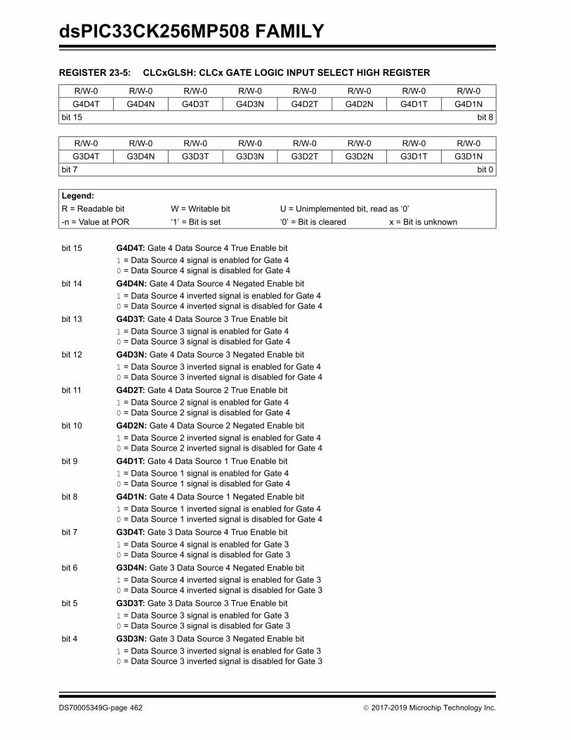
dsPIC33CK256MP508 FAMILY
REGISTER 23-5: CLCxGLSH: CLCx GATE LOGIC INPUT SELECT HIGH REGISTER
R/W-0 R/W-0 R/W-0 R/W-0 R/W-0 R/W-0 R/W-0 R/W-0G4D4T G4D4N G4D3T G4D3N G4D2T G4D2N G4D1T G4D1N
bit 15 bit 8
R/W-0 R/W-0 R/W-0 R/W-0 R/W-0 R/W-0 R/W-0 R/W-0G3D4T G3D4N G3D3T G3D3N G3D2T G3D2N G3D1T G3D1N
bit 7 bit 0
Legend:R = Readable bit W = Writable bit U = Unimplemented bit, read as ‘0’-n = Value at POR ‘1’ = Bit is set ‘0’ = Bit is cleared x = Bit is unknown
bit 15 G4D4T: Gate 4 Data Source 4 True Enable bit1 = Data Source 4 signal is enabled for Gate 40 = Data Source 4 signal is disabled for Gate 4
bit 14 G4D4N: Gate 4 Data Source 4 Negated Enable bit1 = Data Source 4 inverted signal is enabled for Gate 40 = Data Source 4 inverted signal is disabled for Gate 4
bit 13 G4D3T: Gate 4 Data Source 3 True Enable bit1 = Data Source 3 signal is enabled for Gate 40 = Data Source 3 signal is disabled for Gate 4
bit 12 G4D3N: Gate 4 Data Source 3 Negated Enable bit1 = Data Source 3 inverted signal is enabled for Gate 40 = Data Source 3 inverted signal is disabled for Gate 4
bit 11 G4D2T: Gate 4 Data Source 2 True Enable bit1 = Data Source 2 signal is enabled for Gate 40 = Data Source 2 signal is disabled for Gate 4
bit 10 G4D2N: Gate 4 Data Source 2 Negated Enable bit1 = Data Source 2 inverted signal is enabled for Gate 40 = Data Source 2 inverted signal is disabled for Gate 4
bit 9 G4D1T: Gate 4 Data Source 1 True Enable bit1 = Data Source 1 signal is enabled for Gate 40 = Data Source 1 signal is disabled for Gate 4
bit 8 G4D1N: Gate 4 Data Source 1 Negated Enable bit1 = Data Source 1 inverted signal is enabled for Gate 40 = Data Source 1 inverted signal is disabled for Gate 4
bit 7 G3D4T: Gate 3 Data Source 4 True Enable bit1 = Data Source 4 signal is enabled for Gate 30 = Data Source 4 signal is disabled for Gate 3
bit 6 G3D4N: Gate 3 Data Source 4 Negated Enable bit1 = Data Source 4 inverted signal is enabled for Gate 30 = Data Source 4 inverted signal is disabled for Gate 3
bit 5 G3D3T: Gate 3 Data Source 3 True Enable bit1 = Data Source 3 signal is enabled for Gate 30 = Data Source 3 signal is disabled for Gate 3
bit 4 G3D3N: Gate 3 Data Source 3 Negated Enable bit1 = Data Source 3 inverted signal is enabled for Gate 30 = Data Source 3 inverted signal is disabled for Gate 3
DS70005349G-page 462 2017-2019 Microchip Technology Inc.

dsPIC33CK256MP508 FAMILY
bit 3 G3D2T: Gate 3 Data Source 2 True Enable bit1 = Data Source 2 signal is enabled for Gate 30 = Data Source 2 signal is disabled for Gate 3
bit 2 G3D2N: Gate 3 Data Source 2 Negated Enable bit1 = Data Source 2 inverted signal is enabled for Gate 30 = Data Source 2 inverted signal is disabled for Gate 3
bit 1 G3D1T: Gate 3 Data Source 1 True Enable bit1 = Data Source 1 signal is enabled for Gate 30 = Data Source 1 signal is disabled for Gate 3
bit 0 G3D1N: Gate 3 Data Source 1 Negated Enable bit1 = Data Source 1 inverted signal is enabled for Gate 30 = Data Source 1 inverted signal is disabled for Gate 3
REGISTER 23-5: CLCxGLSH: CLCx GATE LOGIC INPUT SELECT HIGH REGISTER (CONTINUED)
2017-2019 Microchip Technology Inc. DS70005349G-page 463

dsPIC33CK256MP508 FAMILY
NOTES:
DS70005349G-page 464 2017-2019 Microchip Technology Inc.

dsPIC33CK256MP508 FAMILY
24.0 PERIPHERAL TRIGGER GENERATOR (PTG)
The dsPIC33CK256MP508 family Peripheral TriggerGenerator (PTG) module is a user-programmablesequencer that is capable of generating complextrigger signal sequences to coordinate the operation ofother peripherals. The PTG module is designed tointerface with the modules, such as an Analog-to-Digital Converter (ADC), output compare and PWMmodules, timers and interrupt controllers.
24.1 Features• Behavior is Step Command Driven:
- Step commands are eight bits wide• Commands are Stored in a Step Queue:
- Queue depth is up to 32 entries- Programmable Step execution time (Step delay)
• Supports the Command Sequence Loop:- Can be nested one-level deep- Conditional or unconditional loop- Two 16-bit loop counters
• 15 Hardware Input Triggers:- Sensitive to either positive or negative edges,
or a high or low level• One Software Input Trigger• Generates up to 32 Unique Output Trigger
Signals• Generates Two Types of Trigger Outputs:
- Individual- Broadcast
• Strobed Output Port for Literal Data Values:- 5-bit literal write (literal part of a command)- 16-bit literal write (literal held in the PTGL0
register)• Generates up to Ten Unique Interrupt Signals• Two 16-Bit General Purpose Timers• Flexible Self-Contained Watchdog Timer (WDT)
to Set an Upper Limit to Trigger Wait Time• Single Step Command Capability in Debug mode• Selectable Clock (System, Pulse-Width Modulator
(PWM) or ADC)• Programmable Clock Divider
Note 1: This data sheet summarizes the featuresof the dsPIC33CK256MP508 family ofdevices. It is not intended to be acomprehensive reference source. Tocomplement the information in this datasheet, refer to “Peripheral TriggerGenerator (PTG)” (www.microchip.com/DS70000669) in the “dsPIC33/PIC24Family Reference Manual”.
2017-2019 Microchip Technology Inc. DS70005349G-page 465

dsPIC33CK256MP508 FAMILY
FIGURE 24-1: PTG BLOCK DIAGRAM16
-Bit
Dat
a Bu
s
PTGQPTR[4:0]
CommandDecoder
PTGHOLD
PTGADJ
PTG WatchdogTimer(1)
PTG Control Logic
PTGWDTIF
PTG GeneralPurposeTimer x
PTG LoopCounter x
Clo
ck In
putsPTGCLK0
PTGCLK[2:0]
PTGL0[15:0] PTGTxLIM[15:0] PTGCxLIM[15:0]
PTGBTE[31:0](2)
PTGO0
PTGSDLIM[15:0]
PTG StepDelay Timer
PTGQUE0PTGQUE1PTGQUE2
PTGQUE3
PTGQUE5PTGQUE4
PTGQUE6PTGQUE7
PTGCST[15:0]
PTGCON[15:0]
PTG
Inte
rrupt
sTr
igge
r Out
puts
Strobe Output[15:0]
Step Command
Step Command
PTGSTEPIF
Trig
ger I
nput
s
PTGO31
•••
PTG0IF
PTG7IF
•••
Step Command
Step Command
PTGDIV[4:0]
...PTGQUE15
Note 1: This is a dedicated Watchdog Timer for the PTG module and is independent of the device Watchdog Timer.2: Some devices support only PTGBTE[15:0] (16 outputs).
PTGCLK7
PTGI0
PTGI15
•••
•••
DS70005349G-page 466 2017-2019 Microchip Technology Inc.

dsPIC33CK256MP508 FAMILY
24.2 PTG Registers
REGISTER 24-1: PTGCST: PTG CONTROL/STATUS LOW REGISTER
R/W-0 U-0 R/W-0 R/W-0 U-0 HC/R/W-0 R/W-0 R/W-0PTGEN — PTGSIDL PTGTOGL — PTGSWT(2) PTGSSEN(3) PTGIVIS
bit 15 bit 8
HC/R/W-0 HS/R/W-0 HS/HC/R/W-0 U-0 U-0 U-0 R/W-0 R/W-0PTGSTRT PTGWDTO PTGBUSY — — — PTGITM1(1) PTGITM0(1)
bit 7 bit 0
Legend: HC = Hardware Clearable bit HS = Hardware Settable bitR = Readable bit W = Writable bit U = Unimplemented bit, read as ‘0’-n = Value at POR ‘1’ = Bit is set ‘0’ = Bit is cleared x = Bit is unknown
bit 15 PTGEN: PTG Enable bit1 = PTG is enabled0 = PTG is disabled
bit 14 Unimplemented: Read as ‘0’ bit 13 PTGSIDL: PTG Freeze in Debug Mode bit
1 = Halts PTG operation when device is Idle0 = PTG operation continues when device is Idle
bit 12 PTGTOGL: PTG Toggle Trigger Output bit1 = Toggles state of TRIG output for each execution of PTGTRIG0 = Generates a single TRIG pulse for each execution of PTGTRIG
bit 11 Unimplemented: Read as ‘0’ bit 10 PTGSWT: PTG Software Trigger bit(2)
1 = If the PTG state machine is executing the “Wait for software trigger” Step command (OPTION[3:0] = 1010or 1011), the command will complete and execution will continue
0 = No action other than to clear the bitbit 9 PTGSSEN: PTG Single-Step Command bit(3)
1 = Enables single Step when in Debug mode0 = Disables single Step
bit 8 PTGIVIS: PTG Counter/Timer Visibility bit1 = Reading the PTGSDLIM, PTGCxLIM or PTGTxLIM registers returns the current values of their
corresponding Counter/Timer registers (PTGSDLIM, PTGCxLIM and PTGTxLIM)0 = Reading the PTGSDLIM, PTGCxLIM or PTGTxLIM registers returns the value of these Limit registers
bit 7 PTGSTRT: PTG Start Sequencer bit1 = Starts to sequentially execute the commands (Continuous mode)0 = Stops executing the commands
bit 6 PTGWDTO: PTG Watchdog Timer Time-out Status bit1 = PTG Watchdog Timer has timed out0 = PTG Watchdog Timer has not timed out
Note 1: These bits apply to the PTGWHI and PTGWLO commands only.2: This bit is only used with the PTGCTRL Step command software trigger option.3: The PTGSSEN bit may only be written when in Debug mode.
2017-2019 Microchip Technology Inc. DS70005349G-page 467

dsPIC33CK256MP508 FAMILY
bit 5 PTGBUSY: PTG State Machine Busy bit1 = PTG is running on the selected clock source; no SFR writes are allowed to PTGCLK[2:0] or
PTGDIV[4:0]0 = PTG state machine is not running
bit 4-2 Unimplemented: Read as ‘0’ bit 1-0 PTGITM[1:0]: PTG Input Trigger Operation Selection bit(1)
11 = Single-level detect with Step delay not executed on exit of command (regardless of the PTGCTRLcommand) (Mode 3)
10 = Single-level detect with Step delay executed on exit of command (Mode 2)01 = Continuous edge detect with Step delay not executed on exit of command (regardless of the
PTGCTRL command) (Mode 1)00 = Continuous edge detect with Step delay executed on exit of command (Mode 0)
REGISTER 24-1: PTGCST: PTG CONTROL/STATUS LOW REGISTER (CONTINUED)
Note 1: These bits apply to the PTGWHI and PTGWLO commands only.2: This bit is only used with the PTGCTRL Step command software trigger option.3: The PTGSSEN bit may only be written when in Debug mode.
DS70005349G-page 468 2017-2019 Microchip Technology Inc.

dsPIC33CK256MP508 FAMILY
REGISTER 24-2: PTGCON: PTG CONTROL/STATUS HIGH REGISTER
R/W-0 R/W-0 R/W-0 R/W-0 R/W-0 R/W-0 R/W-0 R/W-0PTGCLK2 PTGCLK1 PTGCLK0 PTGDIV4 PTGDIV3 PTGDIV2 PTGDIV1 PTGDIV0
bit 15 bit 8
R/W-0 R/W-0 R/W-0 R/W-0 U-0 R/W-0 R/W-0 R/W-0PTGPWD3 PTGPWD2 PTGPWD1 PTGPWD0 — PTGWDT2 PTGWDT1 PTGWDT0
bit 7 bit 0
Legend:R = Readable bit W = Writable bit U = Unimplemented bit, read as ‘0’-n = Value at POR ‘1’ = Bit is set ‘0’ = Bit is cleared x = Bit is unknown
bit 15-13 PTGCLK[2:0]: PTG Module Clock Source Selection bits111 = CLC1110 = PLL VCO DIV 4 output101 = PTG module clock source will be SCCP7100 = PTG module clock source will be SCCP8011 = Input from Timer1 Clock pin, T1CK010 = PTG module clock source will be ADC clock001 = PTG module clock source will be FOSC000 = PTG module clock source will be FOSC/2 (FP)
bit 12-8 PTGDIV[4:0]: PTG Module Clock Prescaler (Divider) bits11111 = Divide-by-3211110 = Divide-by-31...00001 = Divide-by-200000 = Divide-by-1
bit 7-4 PTGPWD[3:0]: PTG Trigger Output Pulse-Width (in PTG clock cycles) bits1111 = All trigger outputs are 16 PTG clock cycles wide1110 = All trigger outputs are 15 PTG clock cycles wide...0001 = All trigger outputs are 2 PTG clock cycles wide0000 = All trigger outputs are 1 PTG clock cycle wide
bit 3 Unimplemented: Read as ‘0’ bit 2-0 PTGWDT[2:0]: PTG Watchdog Timer Time-out Selection bits
111 = Watchdog Timer will time out after 512 PTG clocks110 = Watchdog Timer will time out after 256 PTG clocks101 = Watchdog Timer will time out after 128 PTG clocks100 = Watchdog Timer will time out after 64 PTG clocks011 = Watchdog Timer will time out after 32 PTG clocks010 = Watchdog Timer will time out after 16 PTG clocks001 = Watchdog Timer will time out after 8 PTG clocks000 = Watchdog Timer is disabled
2017-2019 Microchip Technology Inc. DS70005349G-page 469

dsPIC33CK256MP508 FAMILY
REGISTER 24-3: PTGBTE: PTG BROADCAST TRIGGER ENABLE LOW REGISTER(1)
R/W-0 R/W-0 R/W-0 R/W-0 R/W-0 R/W-0 R/W-0 R/W-0PTGBTE[15:8]
bit 15 bit 8
R/W-0 R/W-0 R/W-0 R/W-0 R/W-0 R/W-0 R/W-0 R/W-0PTGBTE[7:0]
bit 7 bit 0
Legend:R = Readable bit W = Writable bit U = Unimplemented bit, read as ‘0’-n = Value at POR ‘1’ = Bit is set ‘0’ = Bit is cleared x = Bit is unknown
bit 15-0 PTGBTE[15:0]: PTG Broadcast Trigger Enable bits1 = Generates trigger when the broadcast command is executed0 = Does not generate trigger when the broadcast command is executed
Note 1: These bits are read-only when the module is executing Step commands.
REGISTER 24-4: PTGBTEH: PTG BROADCAST TRIGGER ENABLE HIGH REGISTER(1)
R/W-0 R/W-0 R/W-0 R/W-0 R/W-0 R/W-0 R/W-0 R/W-0PTGBTE[31:24]
bit 15 bit 8
R/W-0 R/W-0 R/W-0 R/W-0 R/W-0 R/W-0 R/W-0 R/W-0PTGBTE[23:16]
bit 7 bit 0
Legend:R = Readable bit W = Writable bit U = Unimplemented bit, read as ‘0’-n = Value at POR ‘1’ = Bit is set ‘0’ = Bit is cleared x = Bit is unknown
bit 15-0 PTGBTE[31:16]: PTG Broadcast Trigger Enable bits1 = Generates trigger when the broadcast command is executed0 = Does not generate trigger when the broadcast command is executed
Note 1: These bits are read-only when the module is executing Step commands.
DS70005349G-page 470 2017-2019 Microchip Technology Inc.

dsPIC33CK256MP508 FAMILY
REGISTER 24-5: PTGHOLD: PTG HOLD REGISTER(1)
R/W-0 R/W-0 R/W-0 R/W-0 R/W-0 R/W-0 R/W-0 R/W-0PTGHOLD[15:8]
bit 15 bit 8
R/W-0 R/W-0 R/W-0 R/W-0 R/W-0 R/W-0 R/W-0 R/W-0PTGHOLD[7:0]
bit 7 bit 0
Legend:R = Readable bit W = Writable bit U = Unimplemented bit, read as ‘0’-n = Value at POR ‘1’ = Bit is set ‘0’ = Bit is cleared x = Bit is unknown
bit 15-0 PTGHOLD[15:0]: PTG General Purpose Hold Register bitsThis register holds the user-supplied data to be copied to the PTGTxLIM, PTGCxLIM, PTGSDLIM orPTGL0 register using the PTGCOPY command.
Note 1: These bits are read-only when the module is executing Step commands.
REGISTER 24-6: PTGT0LIM: PTG TIMER0 LIMIT REGISTER(1)
R/W-0 R/W-0 R/W-0 R/W-0 R/W-0 R/W-0 R/W-0 R/W-0PTGT0LIM[15:8]
bit 15 bit 8
R/W-0 R/W-0 R/W-0 R/W-0 R/W-0 R/W-0 R/W-0 R/W-0PTGT0LIM[7:0]
bit 7 bit 0
Legend:R = Readable bit W = Writable bit U = Unimplemented bit, read as ‘0’-n = Value at POR ‘1’ = Bit is set ‘0’ = Bit is cleared x = Bit is unknown
bit 15-0 PTGT0LIM[15:0]: PTG Timer0 Limit Register bitsGeneral Purpose Timer0 Limit register.
Note 1: These bits are read-only when the module is executing Step commands.
2017-2019 Microchip Technology Inc. DS70005349G-page 471

dsPIC33CK256MP508 FAMILY
REGISTER 24-7: PTGT1LIM: PTG TIMER1 LIMIT REGISTER(1)
R/W-0 R/W-0 R/W-0 R/W-0 R/W-0 R/W-0 R/W-0 R/W-0PTGT1LIM[15:8]
bit 15 bit 8
R/W-0 R/W-0 R/W-0 R/W-0 R/W-0 R/W-0 R/W-0 R/W-0PTGT1LIM[7:0]
bit 7 bit 0
Legend:R = Readable bit W = Writable bit U = Unimplemented bit, read as ‘0’-n = Value at POR ‘1’ = Bit is set ‘0’ = Bit is cleared x = Bit is unknown
bit 15-0 PTGT1LIM[15:0]: PTG Timer1 Limit Register bitsGeneral Purpose Timer1 Limit register.
Note 1: These bits are read-only when the module is executing Step commands.
REGISTER 24-8: PTGSDLIM: PTG STEP DELAY LIMIT REGISTER(1)
R/W-0 R/W-0 R/W-0 R/W-0 R/W-0 R/W-0 R/W-0 R/W-0PTGSDLIM[15:8]
bit 15 bit 8
R/W-0 R/W-0 R/W-0 R/W-0 R/W-0 R/W-0 R/W-0 R/W-0PTGSDLIM[7:0]
bit 7 bit 0
Legend:R = Readable bit W = Writable bit U = Unimplemented bit, read as ‘0’-n = Value at POR ‘1’ = Bit is set ‘0’ = Bit is cleared x = Bit is unknown
bit 15-0 PTGSDLIM[15:0]: PTG Step Delay Limit Register bitsThis register holds a PTG Step delay value representing the number of additional PTG clocks betweenthe start of a Step command and the completion of a Step command.
Note 1: These bits are read-only when the module is executing Step commands.
DS70005349G-page 472 2017-2019 Microchip Technology Inc.

dsPIC33CK256MP508 FAMILY
REGISTER 24-9: PTGC0LIM: PTG COUNTER 0 LIMIT REGISTER(1)
R/W-0 R/W-0 R/W-0 R/W-0 R/W-0 R/W-0 R/W-0 R/W-0PTGC0LIM[15:8]
bit 15 bit 8
R/W-0 R/W-0 R/W-0 R/W-0 R/W-0 R/W-0 R/W-0 R/W-0PTGC0LIM[7:0]
bit 7 bit 0
Legend:R = Readable bit W = Writable bit U = Unimplemented bit, read as ‘0’-n = Value at POR ‘1’ = Bit is set ‘0’ = Bit is cleared x = Bit is unknown
bit 15-0 PTGC0LIM[15:0]: PTG Counter 0 Limit Register bitsThis register is used to specify the loop count for the PTGJMPC0 Step command or as a Limit registerfor the General Purpose Counter 0.
Note 1: These bits are read-only when the module is executing Step commands.
REGISTER 24-10: PTGC1LIM: PTG COUNTER 1 LIMIT REGISTER(1)
R/W-0 R/W-0 R/W-0 R/W-0 R/W-0 R/W-0 R/W-0 R/W-0PTGC1LIM[15:8]
bit 15 bit 8
R/W-0 R/W-0 R/W-0 R/W-0 R/W-0 R/W-0 R/W-0 R/W-0PTGC1LIM[7:0]
bit 7 bit 0
Legend:R = Readable bit W = Writable bit U = Unimplemented bit, read as ‘0’-n = Value at POR ‘1’ = Bit is set ‘0’ = Bit is cleared x = Bit is unknown
bit 15-0 PTGC1LIM[15:0]: PTG Counter 1 Limit Register bitsThis register is used to specify the loop count for the PTGJMPC1 Step command or as a Limit registerfor the General Purpose Counter 1.
Note 1: These bits are read-only when the module is executing Step commands.
2017-2019 Microchip Technology Inc. DS70005349G-page 473

dsPIC33CK256MP508 FAMILY
REGISTER 24-11: PTGADJ: PTG ADJUST REGISTER(1)
R/W-0 R/W-0 R/W-0 R/W-0 R/W-0 R/W-0 R/W-0 R/W-0PTGADJ[15:8]
bit 15 bit 8
R/W-0 R/W-0 R/W-0 R/W-0 R/W-0 R/W-0 R/W-0 R/W-0PTGADJ[7:0]
bit 7 bit 0
Legend:R = Readable bit W = Writable bit U = Unimplemented bit, read as ‘0’-n = Value at POR ‘1’ = Bit is set ‘0’ = Bit is cleared x = Bit is unknown
bit 15-0 PTGADJ[15:0]: PTG Adjust Register bitsThis register holds the user-supplied data to be added to the PTGTxLIM, PTGCxLIM, PTGSDLIM orPTGL0 register using the PTGADD command.
Note 1: These bits are read-only when the module is executing Step commands.
REGISTER 24-12: PTGL0: PTG LITERAL 0 REGISTER(1,2)
R/W-0 R/W-0 R/W-0 R/W-0 R/W-0 R/W-0 R/W-0 R/W-0PTGL0[15:8]
bit 15 bit 8
R/W-0 R/W-0 R/W-0 R/W-0 R/W-0 R/W-0 R/W-0 R/W-0PTGL0[7:0]
bit 7 bit 0
Legend:R = Readable bit W = Writable bit U = Unimplemented bit, read as ‘0’-n = Value at POR ‘1’ = Bit is set ‘0’ = Bit is cleared x = Bit is unknown
bit 15-0 PTGL0[15:0]: PTG Literal 0 Register bitsThis register holds the 6-bit value to be written to the CNVCHSEL[5:0] bits (ADCON3L[5:0]) with thePTGCTRL Step command.
Note 1: These bits are read-only when the module is executing Step commands.2: The PTG strobe output is typically connected to the ADC Channel Select register. This allows the PTG to
directly control ADC channel switching. See the specific device data sheet for connections of the PTG output.
DS70005349G-page 474 2017-2019 Microchip Technology Inc.

dsPIC33CK256MP508 FAMILY
REGISTER 24-13: PTGQPTR: PTG STEP QUEUE POINTER REGISTER(1)
U-0 U-0 U-0 U-0 U-0 U-0 U-0 U-0— — — — — — — —
bit 15 bit 8
U-0 U-0 U-0 R/W-0 R/W-0 R/W-0 R/W-0 R/W-0— — — PTGQPTR[4:0]
bit 7 bit 0
Legend:R = Readable bit W = Writable bit U = Unimplemented bit, read as ‘0’-n = Value at POR ‘1’ = Bit is set ‘0’ = Bit is cleared x = Bit is unknown
bit 15-5 Unimplemented: Read as ‘0’bit 4-0 PTGQPTR[4:0]: PTG Step Queue Pointer Register bits
This register points to the currently active Step command in the Step queue.
Note 1: These bits are read-only when the module is executing Step commands.
REGISTER 24-14: PTGQUEn: PTG STEP QUEUE n POINTER REGISTER (n = 0-15)(1)
R/W-0 R/W-0 R/W-0 R/W-0 R/W-0 R/W-0 R/W-0 R/W-0STEP2n+1[7:0](2)
bit 15 bit 8
R/W-0 R/W-0 R/W-0 R/W-0 R/W-0 R/W-0 R/W-0 R/W-0STEP2n[7:0](2)
bit 7 bit 0
Legend:R = Readable bit W = Writable bit U = Unimplemented bit, read as ‘0’-n = Value at POR ‘1’ = Bit is set ‘0’ = Bit is cleared x = Bit is unknown
bit 15-8 STEP2n+1[7:0]: PTG Command 4n+1 bits(2)
A queue location for storage of the STEP2n+1 command byte, where ‘n’ is from PTGQUEn.bit STEP2n[7:0]: PTG Command 4n+2 bits(2)
A queue location for storage of the STEP2n command byte, where ‘n’ is the odd numbered StepQueue Pointers.
Note 1: These bits are read-only when the module is executing Step commands.2: Refer to Table 24-1 for the Step command encoding.
2017-2019 Microchip Technology Inc. DS70005349G-page 475

dsPIC33CK256MP508 FAMILY
TABLE 24-1: PTG STEP COMMAND FORMAT AND DESCRIPTION Step Command Byte
STEPx[7:0]CMD[3:0] OPTION[3:0]
bit 7 bit 4 bit 3 bit 0
bit 7-4 Step Command CMD[3:0] Command Description
PTGCTRL 0000 Execute the control command as described by the OPTION[3:0] bits.PTGADD 0001 Add contents of the PTGADJ register to the target register as described by the
OPTION[3:0] bits.PTGCOPY Copy contents of the PTGHOLD register to the target register as described by
the OPTION[3:0] bits.PTGSTRB 001x Copy the values contained in the bits, CMD[0]:OPTION[3:0] to the strobe
output bits [4:0].PTGWHI 0100 Wait for a low-to-high edge input from a selected PTG trigger input as
described by the OPTION[3:0] bits.PTGWLO 0101 Wait for a high-to-low edge input from a selected PTG trigger input as
described by the OPTION[3:0] bits.— 0110 Reserved; do not use.(1)
PTGIRQ 0111 Generate individual interrupt request as described by the OPTION[3:0] bits.PTGTRIG 100x Generate individual trigger output as described by the bits,
CMD[0]:OPTION[3:0].PTGJMP 101x Copy the values contained in the bits, CMD[0]:OPTION[3:0] to the PTGQPTR
register, and jump to that Step queue.PTGJMPC0 110x PTGC0 = PTGC0LIM: Increment the PTGQPTR register.
PTGC0 PTGC0LIM: Increment Counter 0 (PTGC0) and copy the values contained in the bits, CMD[0]:OPTION[3:0] to the PTGQPTR register, and jump to that Step queue.
PTGJMPC1 111x PTGC1 = PTGC1LIM: Increment the PTGQPTR register.PTGC1 PTGC1LIM: Increment Counter 1 (PTGC1) and copy the values contained in the bits, CMD[0]:OPTION[3:0] to the PTGQPTR register, and jump to that Step queue.
Note 1: All reserved commands or options will execute, but they do not have any affect (i.e., execute as a NOP instruction).
DS70005349G-page 476 2017-2019 Microchip Technology Inc.

dsPIC33CK256MP508 FAMILY
TABLE 24-2: PTG COMMAND OPTIONSbit 3-0 Step
Command OPTION[3:0] Command Description
PTGCTRL(1) 0000 NOP.0001 Reserved; do not use.0010 Disable Step delay timer (PTGSD).0011 Reserved; do not use.0100 Reserved; do not use.0101 Reserved; do not use.0110 Enable Step delay timer (PTGSD).0111 Reserved; do not use.1000 Start and wait for the PTG Timer0 to match the PTGT0LIM register.1001 Start and wait for the PTG Timer1 to match the PTGT1LIM register.1010 Wait for the software trigger (level, PTGSWT = 1).1011 Wait for the software trigger (positive edge, PTGSWT = 0 to 1).1100 Copy the PTGC0LIM register contents to the strobe output.1101 Copy the PTGC1LIM register contents to the strobe output.1110 Copy the PTGL0 register contents to the strobe output.1111 Generate the triggers indicated in the PTGBTE register.
PTGADD(1) 0000 Add the PTGADJ register contents to the PTGC0LIM register.0001 Add the PTGADJ register contents to the PTGC1LIM register.0010 Add the PTGADJ register contents to the PTGT0LIM register.0011 Add the PTGADJ register contents to the PTGT1LIM register.0100 Add the PTGADJ register contents to the PTGSDLIM register.0101 Add the PTGADJ register contents to the PTGL0 register.0110 Reserved; do not use.0111 Reserved; do not use.
PTGCOPY(1) 1000 Copy the PTGHOLD register contents to the PTGC0LIM register.1001 Copy the PTGHOLD register contents to the PTGC1LIM register.1010 Copy the PTGHOLD register contents to the PTGT0LIM register.1011 Copy the PTGHOLD register contents to the PTGT1LIM register.1100 Copy the PTGHOLD register contents to the PTGSDLIM register.1101 Copy the PTGHOLD register contents to the PTGL0 register.1110 Reserved; do not use.1111 Reserved; do not use.
Note 1: All reserved commands or options will execute, but they do not have any affect (i.e., execute as a NOP instruction).
2017-2019 Microchip Technology Inc. DS70005349G-page 477

dsPIC33CK256MP508 FAMILY
bit 3-0 Step Command OPTION[3:0] Option Description
PTGWHI(1) or PTGWLO(1)
0000 PTGI0 (see Table 24-3 for input assignments).•••
•••
1111 PTGI15 (see Table 24-3 for input assignments).PTGIRQ(1) 0000 Generate PTG Interrupt 0.
•••
•••
0111 Generate PTG Interrupt 7.1000 Reserved; do not use.•••
•••
1111 Reserved; do not use.PTGTRIG 00000 PTGO0 (see Table 24-4 for output assignments).
00001 PTGO1 (see Table 24-4 for output assignments).•••
•••
11110 PTGO30 (see Table 24-4 for output assignments).11111 PTGO31 (see Table 24-4 for output assignments).
PTGWHI(1) or PTGWLO(1)
0000 PTGI0 (see specific device data sheet for input assignments).•••
•••
1111 PTGI15 (see specific device data sheet for input assignments).PTGIRQ(1) 0000 Generate PTG Interrupt 0 (see specific device data sheet for interrupt
assignments).•••
•••
0111 Generate PTG Interrupt 7 (see specific device data sheet for interrupt assignments).
1000 Reserved; do not use.•••
•••
1111 Reserved; do not use.PTGTRIG 00000 PTGO0 (see specific device data sheet for assignments).
00001 PTGO1 (see specific device data sheet for assignments).
TABLE 24-2: PTG COMMAND OPTIONS (CONTINUED)
Note 1: All reserved commands or options will execute, but they do not have any affect (i.e., execute as a NOP instruction).
DS70005349G-page 478 2017-2019 Microchip Technology Inc.

dsPIC33CK256MP508 FAMILY
TABLE 24-3: PTG INPUT DESCRIPTIONS
TABLE 24-4: PTG OUTPUT DESCRIPTIONS
PTG Input Number PTG Input Description
PTG Trigger Input 0 Trigger Input from PWM1 ADC Trigger 2PTG Trigger Input 1 Trigger Input from PWM2 ADC Trigger 2PTG Trigger Input 2 Trigger Input from PWM3 ADC Trigger 2PTG Trigger Input 3 Trigger Input from PWM4 ADC Trigger 2PTG Trigger Input 4 Trigger Input from PWM5 ADC Trigger 2PTG Trigger Input 5 Trigger Input from PWM6 ADC Trigger 2PTG Trigger Input 6 Trigger Input from PWM7 ADC Trigger 2PTG Trigger Input 7 Trigger Input from SCCP4PTG Trigger Input 8 Trigger Input from SCCP5PTG Trigger Input 9 Trigger Input from Comparator 1PTG Trigger Input 10 Trigger Input from Comparator 2PTG Trigger Input 11 Trigger Input from Comparator 3PTG Trigger Input 12 Trigger Input from CLC1PTG Trigger Input 13 Trigger Input from ADC Done Group InterruptPTG Trigger Input 14 ReservedPTG Trigger Input 15 Trigger Input from INT2 PPS
PTG Output Number PTG Output Description
PTGO0 to PTGO11 ReservedPTGO12 ADC TRGSRC[30]PTGO13 to PTGO23 ReservedPTGO24 PPS Output RP46PTGO25 PPS Output RP47PTGO26 PPS Input RP6PTGO27 PPS Input RP7PTGO28 to PTGO31 Reserved
2017-2019 Microchip Technology Inc. DS70005349G-page 479

dsPIC33CK256MP508 FAMILY
NOTES:
DS70005349G-page 480 2017-2019 Microchip Technology Inc.

dsPIC33CK256MP508 FAMILY
25.0 32-BIT PROGRAMMABLE CYCLIC REDUNDANCY CHECK (CRC) GENERATOR
The 32-bit programmable CRC generator provides ahardware implemented method of quickly generatingchecksums for various networking and securityapplications. It offers the following features:• User-Programmable CRC Polynomial Equation,
up to 32 Bits• Programmable Shift Direction (little or big-endian)• Independent Data and Polynomial Lengths• Configurable Interrupt Output• Data FIFOA simple version of the CRC shift engine is displayed inFigure 25-1.
FIGURE 25-1: CRC MODULE BLOCK DIAGRAM
Note 1: This data sheet summarizes the featuresof the dsPIC33CK256MP508 family ofdevices. It is not intended to be a com-prehensive reference source. For moreinformation, refer to “32-Bit Programma-ble Cyclic Redundancy Check (CRC)”(www.microchip.com/DS30009729) in the“dsPIC33/PIC24 Family ReferenceManual”.
CRCInterrupt
Variable FIFO(4x32, 8x16 or 16x8)
CRCDATH CRCDATL
Shift BufferCRC Shift Engine
CRCWDATH CRCWDATL
Shifter Clock2 * FCY
LENDIAN
CRCISEL
1
0
FIFO Empty
ShiftComplete
1
0
2017-2019 Microchip Technology Inc. DS70005349G-page 481

dsPIC33CK256MP508 FAMILY
25.1 Control Registers
REGISTER 25-1: CRCCONL: CRC CONTROL REGISTER LOW
R/W-0 U-0 R/W-0 HSC/R-0 HSC/R-0 HSC/R-0 HSC/R-0 HSC/R-0CRCEN — CSIDL VWORD4 VWORD3 VWORD2 VWORD1 VWORD0
bit 15 bit 8
HSC/R-0 HSC/R-1 R/W-0 HC/R/W-0 R/W-0 R/W-0 U-0 U-0CRCFUL CRCMPT CRCISEL CRCGO LENDIAN MOD — —
bit 7 bit 0
Legend: HC = Hardware Clearable bit HSC = Hardware Settable/Clearable bitR = Readable bit W = Writable bit U = Unimplemented bit, read as ‘0’-n = Value at POR ‘1’ = Bit is set ‘0’ = Bit is cleared x = Bit is unknown
bit 15 CRCEN: CRC Enable bit1 = Enables module0 = Disables module
bit 14 Unimplemented: Read as ‘0’bit 13 CSIDL: CRC Stop in Idle Mode bit
1 = Discontinues module operation when device enters Idle mode0 = Continues module operation in Idle mode
bit 12-8 VWORD[4:0]: Pointer Value bitsIndicates the number of valid words in the FIFO. Has a maximum value of 8 when PLEN[4:0] 7 or16 when PLEN[4:0] 7.
bit 7 CRCFUL: CRC FIFO Full bit1 = FIFO is full 0 = FIFO is not full
bit 6 CRCMPT: CRC FIFO Empty bit1 = FIFO is empty 0 = FIFO is not empty
bit 5 CRCISEL: CRC Interrupt Selection bit1 = Interrupt on FIFO is empty; the final word of data is still shifting through the CRC0 = Interrupt on shift is complete and results are ready
bit 4 CRCGO: CRC Start bit1 = Starts CRC serial shifter0 = CRC serial shifter is turned off
bit 3 LENDIAN: Data Shift Direction Select bit1 = Data word is shifted into the FIFO, starting with the LSb (little-endian)0 = Data word is shifted into the FIFO, starting with the MSb (big-endian)
bit 2 MOD: CRC Calculation Mode bit 1 = Alternate mode 0 = Legacy mode bit
bit 1-0 Unimplemented: Read as ‘0’
DS70005349G-page 482 2017-2019 Microchip Technology Inc.

dsPIC33CK256MP508 FAMILY
REGISTER 25-2: CRCCONH: CRC CONTROL REGISTER HIGH
U-0 U-0 U-0 R/W-0 R/W-0 R/W-0 R/W-0 R/W-0— — — DWIDTH4 DWIDTH3 DWIDTH2 DWIDTH1 DWIDTH0
bit 15 bit 8
U-0 U-0 U-0 R/W-0 R/W-0 R/W-0 R/W-0 R/W-0— — — PLEN4 PLEN3 PLEN2 PLEN1 PLEN0
bit 7 bit 0
Legend:R = Readable bit W = Writable bit U = Unimplemented bit, read as ‘0’-n = Value at POR ‘1’ = Bit is set ‘0’ = Bit is cleared x = Bit is unknown
bit 15-13 Unimplemented: Read as ‘0’bit 12-8 DWIDTH[4:0]: Data Word Width Configuration bits
Configures the width of the data word (Data Word Width – 1).bit 7-5 Unimplemented: Read as ‘0’bit 4-0 PLEN[4:0]: Polynomial Length Configuration bits
Configures the length of the polynomial (Polynomial Length – 1).
2017-2019 Microchip Technology Inc. DS70005349G-page 483

dsPIC33CK256MP508 FAMILY
REGISTER 25-3: CRCXORL: CRC XOR POLYNOMIAL REGISTER, LOW
R/W-0 R/W-0 R/W-0 R/W-0 R/W-0 R/W-0 R/W-0 R/W-0X[15:8]
bit 15 bit 8
R/W-0 R/W-0 R/W-0 R/W-0 R/W-0 R/W-0 R/W-0 U-0X[7:1] —
bit 7 bit 0
Legend:R = Readable bit W = Writable bit U = Unimplemented bit, read as ‘0’-n = Value at POR ‘1’ = Bit is set ‘0’ = Bit is cleared x = Bit is unknown
bit 15-1 X[15:1]: XOR of Polynomial Term xn Enable bitsbit 0 Unimplemented: Read as ‘0’
REGISTER 25-4: CRCXORH: CRC XOR POLYNOMIAL REGISTER, HIGH
R/W-0 R/W-0 R/W-0 R/W-0 R/W-0 R/W-0 R/W-0 R/W-0X[31:24]
bit 15 bit 8
R/W-0 R/W-0 R/W-0 R/W-0 R/W-0 R/W-0 R/W-0 R/W-0X[23:16]
bit 7 bit 0
Legend:R = Readable bit W = Writable bit U = Unimplemented bit, read as ‘0’-n = Value at POR ‘1’ = Bit is set ‘0’ = Bit is cleared x = Bit is unknown
bit 15-0 X[31:16]: XOR of Polynomial Term xn Enable bits
DS70005349G-page 484 2017-2019 Microchip Technology Inc.

dsPIC33CK256MP508 FAMILY
26.0 CURRENT BIAS GENERATOR (CBG)
The Current Bias Generator (CBG) consists of twoclasses of current sources: 10 μA and 50 μA sources.The major features of each current source are:• 10 μA Current Sources:
- Current sourcing only- Up to four independent sources
• 50 μA Current Sources:- Selectable current sourcing or sinking- Selectable current mirroring for sourcing and
sinkingA simplified block diagram of the CBG module isshown in Figure 26-1.
TABLE 26-1: CBG CHANNEL AVAILABILITY
FIGURE 26-1: CONSTANT-CURRENT SOURCE MODULE BLOCK DIAGRAM(2)
Note 1: This data sheet summarizes the featuresof the dsPIC33CK256MP508 family ofdevices. It is not intended to be a compre-hensive reference source. To complementthe information in this data sheet, refer to“Current Bias Generator (CBG)”(www.microchip.com/DS70005253) in the“dsPIC33/PIC24 Family ReferenceManual”.
2: Some registers and associated bitsdescribed in this section may not be avail-able on all devices. Refer to Table 26-1 forCBG channel availability on packagevariants. Package Type ISRCx IBIASx
28-pin — 0,336-pin 0,1 0,2,348-pin 0,1,2,3 0,1,2,364-pin 0,1,2,3 0,1,2,380-pin 0,1,2,3 0,1,2,3
Note 1: RESD is typically 300 Ohms; for more information, refer to the device data sheet.2: In Figure 26-1, the ADC analog input is shown for clarity. Each analog peripheral connected to the pin has a
separate Electrostatic Discharge (ESD) resistor.
AVDD
ONI10ENx
RESD(1) ISRCx
ADC
ADC
RESD(1)
RESD(1)
IBIASx
AVSS
AVDD
10 µA Source 50 µA Source
ONSRCENx
ONSNKENx
2017-2019 Microchip Technology Inc. DS70005349G-page 485

dsPIC33CK256MP508 FAMILY
26.1 Current Bias Generator Control Registers
REGISTER 26-1: BIASCON: CURRENT BIAS GENERATOR CONTROL REGISTER
R/W-0 U-0 U-0 U-0 U-0 U-0 U-0 U-0ON — — — — — — —
bit 15 bit 8
U-0 U-0 U-0 U-0 R/W-0 R/W-0 R/W-0 R/W-0— — — — I10EN3 I10EN2 I10EN1 I10EN0
bit 7 bit 0
Legend:R = Readable bit W = Writable bit U = Unimplemented bit, read as ‘0’-n = Value at POR ‘1’ = Bit is set ‘0’ = Bit is cleared x = Bit is unknown
bit 15 ON: Current Bias Module Enable bit1 = Module is enabled0 = Module is disabled
bit 14-4 Unimplemented: Read as ‘0’bit 3 I10EN3: 10 μA Enable for Output 3 bit
1 = 10 μA output is enabled0 = 10 μA output is disabled
bit 2 I10EN2: 10 μA Enable for Output 2 bit1 = 10 μA output is enabled0 = 10 μA output is disabled
bit 1 I10EN1: 10 μA Enable for Output 1 bit1 = 10 μA output is enabled0 = 10 μA output is disabled
bit 0 I10EN0: 10 μA Enable for Output 0 bit1 = 10 μA output is enabled0 = 10 μA output is disabled
DS70005349G-page 486 2017-2019 Microchip Technology Inc.

dsPIC33CK256MP508 FAMILY
REGISTER 26-2: IBIASCONH: CURRENT BIAS GENERATOR 50 μA CURRENT SOURCE CONTROL HIGH REGISTER
U-0 U-0 R/W-0 R/W-0 R/W-0 R/W-0 R/W-0 R/W-0— — SHRSRCEN3 SHRSNKEN3 GENSRCEN3 GENSNKEN3 SRCEN3 SNKEN3
bit 15 bit 8
U-0 U-0 R/W-0 R/W-0 R/W-0 R/W-0 R/W-0 R/W-0— — SHRSRCEN2 SHRSNKEN2 GENSRCEN2 GENSNKEN2 SRCEN2 SNKEN2
bit 7 bit 0
Legend:R = Readable bit W = Writable bit U = Unimplemented bit, read as ‘0’-n = Value at POR ‘1’ = Bit is set ‘0’ = Bit is cleared x = Bit is unknown
bit 15-14 Unimplemented: Read as ‘0’bit 13 SHRSRCEN3: Share Source Enable for Output #3 bit
1 = Sourcing Current Mirror mode is enabled (uses reference from another source)0 = Sourcing Current Mirror mode is disabled
bit 12 SHRSNKEN3: Share Sink Enable for Output #3 bit1 = Sinking Current Mirror mode is enabled (uses reference from another source)0 = Sinking Current Mirror mode is disabled
bit 11 GENSRCEN3: Generated Source Enable for Output #3 bit1 = Source generates the current source mirror reference0 = Source does not generate the current source mirror reference
bit 10 GENSNKEN3: Generated Sink Enable for Output #3 bit1 = Source generates the current sink mirror reference0 = Source does not generate the current sink mirror reference
bit 9 SRCEN3: Source Enable for Output #3 bit1 = Current source is enabled0 = Current source is disabled
bit 8 SNKEN3: Sink Enable for Output #3 bit1 = Current sink is enabled0 = Current sink is disabled
bit 7-6 Unimplemented: Read as ‘0’bit 5 SHRSRCEN2: Share Source Enable for Output #2 bit
1 = Sourcing Current Mirror mode is enabled (uses reference from another source)0 = Sourcing Current Mirror mode is disabled
bit 4 SHRSNKEN2: Share Sink Enable for Output #2 bit1 = Sinking Current Mirror mode is enabled (uses reference from another source)0 = Sinking Current Mirror mode is disabled
bit 3 GENSRCEN2: Generated Source Enable for Output #2 bit1 = Source generates the current source mirror reference0 = Source does not generate the current source mirror reference
bit 2 GENSNKEN2: Generated Sink Enable for Output #2 bit1 = Source generates the current sink mirror reference0 = Source does not generate the current sink mirror reference
bit 1 SRCEN2: Source Enable for Output #2 bit1 = Current source is enabled0 = Current source is disabled
bit 0 SNKEN2: Sink Enable for Output #2 bit1 = Current sink is enabled0 = Current sink is disabled
2017-2019 Microchip Technology Inc. DS70005349G-page 487
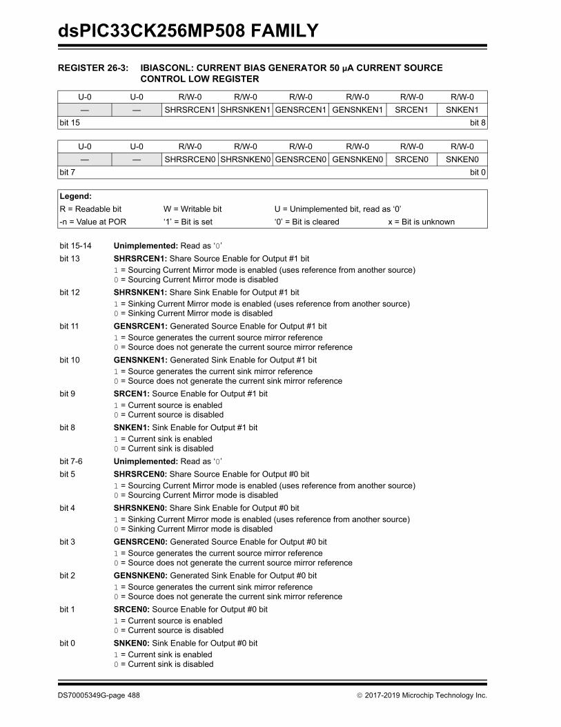
dsPIC33CK256MP508 FAMILY
REGISTER 26-3: IBIASCONL: CURRENT BIAS GENERATOR 50 μA CURRENT SOURCECONTROL LOW REGISTER
U-0 U-0 R/W-0 R/W-0 R/W-0 R/W-0 R/W-0 R/W-0— — SHRSRCEN1 SHRSNKEN1 GENSRCEN1 GENSNKEN1 SRCEN1 SNKEN1
bit 15 bit 8
U-0 U-0 R/W-0 R/W-0 R/W-0 R/W-0 R/W-0 R/W-0— — SHRSRCEN0 SHRSNKEN0 GENSRCEN0 GENSNKEN0 SRCEN0 SNKEN0
bit 7 bit 0
Legend:R = Readable bit W = Writable bit U = Unimplemented bit, read as ‘0’-n = Value at POR ‘1’ = Bit is set ‘0’ = Bit is cleared x = Bit is unknown
bit 15-14 Unimplemented: Read as ‘0’bit 13 SHRSRCEN1: Share Source Enable for Output #1 bit
1 = Sourcing Current Mirror mode is enabled (uses reference from another source)0 = Sourcing Current Mirror mode is disabled
bit 12 SHRSNKEN1: Share Sink Enable for Output #1 bit1 = Sinking Current Mirror mode is enabled (uses reference from another source)0 = Sinking Current Mirror mode is disabled
bit 11 GENSRCEN1: Generated Source Enable for Output #1 bit1 = Source generates the current source mirror reference0 = Source does not generate the current source mirror reference
bit 10 GENSNKEN1: Generated Sink Enable for Output #1 bit1 = Source generates the current sink mirror reference0 = Source does not generate the current sink mirror reference
bit 9 SRCEN1: Source Enable for Output #1 bit1 = Current source is enabled0 = Current source is disabled
bit 8 SNKEN1: Sink Enable for Output #1 bit1 = Current sink is enabled0 = Current sink is disabled
bit 7-6 Unimplemented: Read as ‘0’bit 5 SHRSRCEN0: Share Source Enable for Output #0 bit
1 = Sourcing Current Mirror mode is enabled (uses reference from another source)0 = Sourcing Current Mirror mode is disabled
bit 4 SHRSNKEN0: Share Sink Enable for Output #0 bit1 = Sinking Current Mirror mode is enabled (uses reference from another source)0 = Sinking Current Mirror mode is disabled
bit 3 GENSRCEN0: Generated Source Enable for Output #0 bit1 = Source generates the current source mirror reference0 = Source does not generate the current source mirror reference
bit 2 GENSNKEN0: Generated Sink Enable for Output #0 bit1 = Source generates the current sink mirror reference0 = Source does not generate the current sink mirror reference
bit 1 SRCEN0: Source Enable for Output #0 bit1 = Current source is enabled0 = Current source is disabled
bit 0 SNKEN0: Sink Enable for Output #0 bit1 = Current sink is enabled0 = Current sink is disabled
DS70005349G-page 488 2017-2019 Microchip Technology Inc.

dsPIC33CK256MP508 FAMILY
27.0 OPERATIONAL AMPLIFIER
The dsPIC33CK256MP508 family implements threeinstances of operational amplifiers (op amps). Theop amps can be used for a wide variety of purposes,including signal conditioning and filtering. The threeop amps are functionally identical. The block diagramfor a single amplifier is shown in Figure 27-1.
FIGURE 27-1: SINGLE OPERATIONAL AMPLIFIER BLOCK DIAGRAM
The op amps are controlled by two SFR registers:AMPCON1L and AMPCON1H. They remain in a low-power state until the AMPON bit is set. Each op ampcan then be enabled independently by setting thecorresponding AMPENx bit (x = 1, 2, 3). The NCHDISx bit provides some flexibility regardinginput range versus Integral Nonlinearity (INL). WhenNCHDISx = 0 (default), the op amps have a wider inputvoltage range (see Table 33-41 in Section 33.0 “Elec-trical Characteristics”). When NCHDISx = 1, the widerinput range is traded for improved INL performance(lower INL).
Note: Some device variants support onlytwo op amp instances. Refer to Table 1and Table 2 for availability.
OAxOUTOAxIN-
OAxIN+
–
+
2017-2019 Microchip Technology Inc. DS70005349G-page 489

dsPIC33CK256MP508 FAMILY
27.1 Operational Amplifier Control Registers REGISTER 27-1: AMPCON1L: OP AMP CONTROL REGISTER LOW
R/W-0 U-0 U-0 U-0 U-0 U-0 U-0 U-0AMPON — — — — — — —
bit 15 bit 8
U-0 U-0 U-0 U-0 U-0 R/W-0 R/W-0 R/W-0— — — — — AMPEN3 AMPEN2 AMPEN1
bit 7 bit 0
Legend:R = Readable bit W = Writable bit U = Unimplemented bit, read as ‘0’-n = Value at POR ‘1’ = Bit is set ‘0’ = Bit is cleared x = Bit is unknown
bit 15 AMPON: Op Amp Enable/On bit1 = Enables op amp modules if their respective AMPENx bits are also asserted0 = Disables all op amp modules
bit 14-3 Unimplemented: Read as ‘0’bit 2 AMPEN3: Op Amp #3 Enable bit
1 = Enables Op Amp #3 if the AMPON bit is also asserted0 = Disables Op Amp #3
bit 1 AMPEN2: Op Amp #2 Enable bit1 = Enables Op Amp #2 if the AMPON bit is also asserted0 = Disables Op Amp #2
bit 0 AMPEN1: Op Amp #1 Enable bit1 = Enables Op Amp #1 if the AMPON bit is also asserted0 = Disables Op Amp #1
DS70005349G-page 490 2017-2019 Microchip Technology Inc.

dsPIC33CK256MP508 FAMILY
REGISTER 27-2: AMPCON1H: OP AMP CONTROL REGISTER HIGH
U-0 U-0 U-0 U-0 U-0 U-0 U-0 U-0— — — — — — — —
bit 15 bit 8
U-0 U-0 U-0 U-0 U-0 R/W-0 R/W-0 R/W-0— — — — — NCHDIS3 NCHDIS2 NCHDIS1
bit 7 bit 0
Legend:R = Readable bit W = Writable bit U = Unimplemented bit, read as ‘0’-n = Value at POR ‘1’ = Bit is set ‘0’ = Bit is cleared x = Bit is unknown
bit 15-3 Unimplemented: Read as ‘0’bit 2 NCHDIS3: Op Amp #3 N Channel Disable bit
1 = Disables Op Amp #3 N channels input stage; reduced INL, but lowered input voltage range0 = Wide input range for Op Amp #3
bit 1 NCHDIS2: Op Amp #2 N Channel Disable bit1 = Disables Op Amp #2 N channels input stage; reduced INL, but lowered input voltage range0 = Wide input range for Op Amp #2
bit 0 NCHDIS1: Op Amp #1 N Channel Disable bit1 = Disables Op Amp #1 N channels input stage; reduced INL, but lowered input voltage range0 = Wide input range for Op Amp #1
2017-2019 Microchip Technology Inc. DS70005349G-page 491

dsPIC33CK256MP508 FAMILY
NOTES:
DS70005349G-page 492 2017-2019 Microchip Technology Inc.

dsPIC33CK256MP508 FAMILY
28.0 DEADMAN TIMER (DMT)
The primary function of the Deadman Timer (DMT) is tointerrupt the processor in the event of a software mal-function. The DMT, which works on the system clock, isa free-running instruction fetch timer, which is clocked
whenever an instruction fetch occurs, until a countmatch occurs. Instructions are not fetched when theprocessor is in Sleep mode.DMT can be enabled in the Configuration fuse or bysoftware in the DMTCON register by setting the ON bit.The DMT consists of a 32-bit counter with a time-outcount match value, as specified by the two 16-bitConfiguration Fuse registers: FDMTCNTL andFDMTCNTH. A DMT is typically used in mission-critical and safety-critical applications, where any single failure of thesoftware functionality and sequencing must bedetected.
Figure 28-1 shows a block diagram of the DeadmanTimer module.
FIGURE 28-1: DEADMAN TIMER BLOCK DIAGRAM
Note 1: This data sheet summarizes the featuresof the dsPIC33CK256MP508 family ofdevices. It is not intended to be acomprehensive reference source. Tocomplement the information in this datasheet, refer to “Deadman Timer (DMT)”(www.microchip.com/DS70005155) in the“dsPIC33/PIC24 Family ReferenceManual”.
32-Bit Counter
System Clock
DMT EventInstruction Fetched Strobe(2)
Improper Sequence
(Counter) = DMT Max Count(1)
Note 1: DMT Max Count is controlled by the initial value of the FDMTCNTL and FDMTCNTH Configuration registers.2: DMT window interval is controlled by the value of the FDMTIVTL and FDMTIVTH Configuration registers.
Flag
DMT Enable
BAD1
BAD2
2017-2019 Microchip Technology Inc. DS70005349G-page 493

dsPIC33CK256MP508 FAMILY
28.1 Deadman Timer Control Registers
REGISTER 28-1: DMTCON: DEADMAN TIMER CONTROL REGISTER
R/W-0 U-0 U-0 U-0 U-0 U-0 U-0 U-0ON(1) — — — — — — —
bit 15 bit 8
U-0 U-0 U-0 U-0 U-0 U-0 U-0 U-0— — — — — — — —
bit 7 bit 0
Legend:R = Readable bit W = Writable bit U = Unimplemented bit, read as ‘0’-n = Value at POR ‘1’ = Bit is set ‘0’ = Bit is cleared x = Bit is unknown
bit 15 ON: DMT Module Enable bit(1)
1 = Deadman Timer module is enabled 0 = Deadman Timer module is not enabled
bit 14-0 Unimplemented: Read as ‘0’
Note 1: This bit has control only when DMTDIS = 0 in the FDMT register.
REGISTER 28-2: DMTPRECLR: DEADMAN TIMER PRECLEAR REGISTER
R/W-0 R/W-0 R/W-0 R/W-0 R/W-0 R/W-0 R/W-0 R/W-0STEP1[7:0]
bit 15 bit 8
U-0 U-0 U-0 U-0 U-0 U-0 U-0 U-0— — — — — — — —
bit 7 bit 0
Legend:R = Readable bit W = Writable bit U = Unimplemented bit, read as ‘0’-n = Value at POR ‘1’ = Bit is set ‘0’ = Bit is cleared x = Bit is unknown
bit 15-8 STEP1[7:0]: DMT Preclear Enable bits01000000 = Enables the Deadman Timer preclear (Step 1)All Other Write Patterns = Sets the BAD1 flag; these bits are cleared when a DMT Reset event occurs.
STEP1[7:0] bits are also cleared if the STEP2[7:0] bits are loaded with the correctvalue in the correct sequence.
bit 7-0 Unimplemented: Read as ‘0’
DS70005349G-page 494 2017-2019 Microchip Technology Inc.

dsPIC33CK256MP508 FAMILY
REGISTER 28-3: DMTCLR: DEADMAN TIMER CLEAR REGISTER
U-0 U-0 U-0 U-0 U-0 U-0 U-0 U-0— — — — — — — —
bit 15 bit 8
R/W-0 R/W-0 R/W-0 R/W-0 R/W-0 R/W-0 R/W-0 R/W-0STEP2[7:0]
bit 7 bit 0
Legend:R = Readable bit W = Writable bit U = Unimplemented bit, read as ‘0’-n = Value at POR ‘1’ = Bit is set ‘0’ = Bit is cleared x = Bit is unknown
bit 15-8 Unimplemented: Read as ‘0’bit 7-0 STEP2[7:0]: DMT Clear Timer bits
00001000 = Clears STEP1[7:0], STEP2[7:0] and the Deadman Timer if preceded by the correctloading of the STEP1[7:0] bits in the correct sequence. The write to these bits may beverified by reading the DMTCNTL/H register and observing the counter being reset.
All Other Write Patterns = Sets the BAD2 bit; the value of STEP1[7:0] will remain unchanged and the new value
being written to STEP2[7:0] will be captured. These bits are cleared when a DMTReset event occurs.
2017-2019 Microchip Technology Inc. DS70005349G-page 495

dsPIC33CK256MP508 FAMILY
REGISTER 28-4: DMTSTAT: DEADMAN TIMER STATUS REGISTER
U-0 U-0 U-0 U-0 U-0 U-0 U-0 U-0— — — — — — — —
bit 15 bit 8
HC/R-0 HC/R-0 HC/R-0 U-0 U-0 U-0 U-0 R-0BAD1 BAD2 DMTEVENT — — — — WINOPN
bit 7 bit 0
Legend: HC = Hardware Clearable bitR = Readable bit W = Writable bit U = Unimplemented bit, read as ‘0’-n = Value at POR ‘1’ = Bit is set ‘0’ = Bit is cleared x = Bit is unknown
bit 15-8 Unimplemented: Read as ‘0’bit 7 BAD1: Deadman Timer Bad STEP1[7:0] Value Detect bit
1 = Incorrect STEP1[7:0] value was detected0 = Incorrect STEP1[7:0] value was not detected
bit 6 BAD2: Deadman Timer Bad STEP2[7:0] Value Detect bit1 = Incorrect STEP2[7:0] value was detected0 = Incorrect STEP2[7:0] value was not detected
bit 5 DMTEVENT: Deadman Timer Event bit1 = Deadman Timer event was detected (counter expired, or bad STEP1[7:0] or STEP2[7:0] value
was entered prior to counter increment)0 = Deadman Timer event was not detected
bit 4-1 Unimplemented: Read as ‘0’bit 0 WINOPN: Deadman Timer Clear Window bit
1 = Deadman Timer clear window is open0 = Deadman Timer clear window is not open
DS70005349G-page 496 2017-2019 Microchip Technology Inc.

dsPIC33CK256MP508 FAMILY
REGISTER 28-5: DMTCNTL: DEADMAN TIMER COUNT REGISTER LOW
R-0 R-0 R-0 R-0 R-0 R-0 R-0 R-0COUNTER[15:8]
bit 15 bit 8
R-0 R-0 R-0 R-0 R-0 R-0 R-0 R-0COUNTER[7:0]
bit 7 bit 0
Legend:R = Readable bit W = Writable bit U = Unimplemented bit, read as ‘0’-n = Value at POR ‘1’ = Bit is set ‘0’ = Bit is cleared x = Bit is unknown
bit 15-0 COUNTER[15:0]: Read Current Contents of Lower DMT Counter bits
REGISTER 28-6: DMTCNTH: DEADMAN TIMER COUNT REGISTER HIGH
R-0 R-0 R-0 R-0 R-0 R-0 R-0 R-0COUNTER[31:24]
bit 15 bit 8
R-0 R-0 R-0 R-0 R-0 R-0 R-0 R-0COUNTER[23:16]
bit 7 bit 0
Legend:R = Readable bit W = Writable bit U = Unimplemented bit, read as ‘0’-n = Value at POR ‘1’ = Bit is set ‘0’ = Bit is cleared x = Bit is unknown
bit 15-0 COUNTER[31:16]: Read Current Contents of Higher DMT Counter bits
2017-2019 Microchip Technology Inc. DS70005349G-page 497

dsPIC33CK256MP508 FAMILY
REGISTER 28-7: DMTPSCNTL: DMT POST-CONFIGURE COUNT STATUS REGISTER LOW
R-y R-y R-y R-y R-y R-y R-y R-yPSCNT[15:8]
bit 15 bit 8
Ry R-y R-y R-y R-y R-y R-y R-yPSCNT[7:0]
bit 7 bit 0
Legend: y = Value from Configuration bit on PORR = Readable bit W = Writable bit U = Unimplemented bit, read as ‘0’-n = Value at POR ‘1’ = Bit is set ‘0’ = Bit is cleared x = Bit is unknown
bit 15-0 PSCNT[15:0]: Lower DMT Instruction Count Value Configuration Status bitsThis is always the value of the FDMTCNTL Configuration register.
REGISTER 28-8: DMTPSCNTH: DMT POST-CONFIGURE COUNT STATUS REGISTER HIGH
R-y R-y R-y R-y R-y R-y R-y R-yPSCNT[31:24]
bit 15 bit 8
R-y R-y R-y R-y R-y R-y R-y R-yPSCNT[23:16]
bit 7 bit 0
Legend: y = Value from Configuration bit on PORR = Readable bit W = Writable bit U = Unimplemented bit, read as ‘0’-n = Value at POR ‘1’ = Bit is set ‘0’ = Bit is cleared x = Bit is unknown
bit 15-0 PSCNT[31:16]: Higher DMT Instruction Count Value Configuration Status bitsThis is always the value of the FDMTCNTH Configuration register.
DS70005349G-page 498 2017-2019 Microchip Technology Inc.

dsPIC33CK256MP508 FAMILY
REGISTER 28-9: DMTPSINTVL: DMT POST-CONFIGURE INTERVAL STATUS REGISTER LOW
R-y R-y R-y R-y R-y R-y R-y R-yPSINTV[15:8]
bit 15 bit 8
R-y R-y R-y R-y R-y R-y R-y R-yPSINTV[7:0]
bit 7 bit 0
Legend: y = Value from Configuration bit on PORR = Readable bit W = Writable bit U = Unimplemented bit, read as ‘0’-n = Value at POR ‘1’ = Bit is set ‘0’ = Bit is cleared x = Bit is unknown
bit 15-0 PSINTV[15:0]: Lower DMT Window Interval Configuration Status bitsThis is always the value of the FDMTIVTL Configuration register.
REGISTER 28-10: DMTPSINTVH: DMT POST-CONFIGURE INTERVAL STATUS REGISTER HIGH
R-y R-y R-y R-y R-y R-y R-y R-yPSINTV[31:24]
bit 15 bit 8
R-y R-y R-y R-y R-y R-y R-y R-yPSINTV[23:16]
bit 7 bit 0
Legend: y = Value from Configuration bit on PORR = Readable bit W = Writable bit U = Unimplemented bit, read as ‘0’-n = Value at POR ‘1’ = Bit is set ‘0’ = Bit is cleared x = Bit is unknown
bit 15-0 PSINTV[31:16]: Higher DMT Window Interval Configuration Status bitsThis is always the value of the FDMTIVTH Configuration register.
2017-2019 Microchip Technology Inc. DS70005349G-page 499

dsPIC33CK256MP508 FAMILY
REGISTER 28-11: DMTHOLDREG: DMT HOLD REGISTER(1)
R-0 R-0 R-0 R-0 R-0 R-0 R-0 R-0UPRCNT[15:8]
bit 15 bit 8
R-0 R-0 R-0 R-0 R-0 R-0 R-0 R-0UPRCNT[7:0]
bit 7 bit 0
Legend:R = Readable bit W = Writable bit U = Unimplemented bit, read as ‘0’-n = Value at POR ‘1’ = Bit is set ‘0’ = Bit is cleared x = Bit is unknown
bit 15-0 UPRCNT[15:0]: DMTCNTH Register Value when DMTCNTL and DMTCNTH were Last Read bits
Note 1: The DMTHOLDREG register is initialized to ‘0’ on Reset, and is only loaded when the DMTCNTL and DMTCNTH registers are read.
DS70005349G-page 500 2017-2019 Microchip Technology Inc.

dsPIC33CK256MP508 FAMILY
29.0 POWER-SAVING FEATURES
The dsPIC33CK256MP508 family devices providethe ability to manage power consumption byselectively managing clocking to the CPU and theperipherals. In general, a lower clock frequency anda reduction in the number of peripherals beingclocked constitutes lower consumed power.dsPIC33CK256MP508 family devices can managepower consumption in four ways:• Clock Frequency• Instruction-Based Sleep and Idle modes• Software-Controlled Doze mode• Selective Peripheral Control in SoftwareCombinations of these methods can be used toselectively tailor an application’s power consumptionwhile still maintaining critical application features, suchas timing-sensitive communications.
29.1 Clock Frequency and Clock Switching
The dsPIC33CK256MP508 family devices allow a widerange of clock frequencies to be selected under appli-cation control. If the system clock configuration is notlocked, users can choose low-power or high-precisionoscillators by simply changing the NOSCx bits(OSCCON[10:8]). The process of changing a systemclock during operation, as well as limitations to theprocess, are discussed in more detail in Section 9.0“Oscillator with High-Frequency PLL”.
29.2 Instruction-Based Power-Saving Modes
The dsPIC33CK256MP508 family devices have twospecial power-saving modes that are enteredthrough the execution of a special PWRSAV instruc-tion. Sleep mode stops clock operation and halts allcode execution. Idle mode halts the CPU and codeexecution, but allows peripheral modules to continueoperation. The assembler syntax of the PWRSAVinstruction is shown in Example 29-1.
Sleep and Idle modes can be exited as a result of anenabled interrupt, WDT time-out or a device Reset. Whenthe device exits these modes, it is said to “wake-up”.
EXAMPLE 29-1: PWRSAV INSTRUCTION SYNTAX IN ASSEMBLY
EXAMPLE 29-2: PWRSAV INSTRUCTION SYNTAX IN C LANGUAGE
Note 1: This data sheet summarizes thefeatures of the dsPIC33CK256MP508family of devices. It is not intended to be acomprehensive reference source. To com-plement the information in this data sheet,refer to “Watchdog Timer and Power-Saving Modes” (www.microchip.com/DS70615) in the “dsPIC33/PIC24 FamilyReference Manual”.
Note: SLEEP_MODE and IDLE_MODE are con-stants defined in the assembler includefile for the selected device.
PWRSAV #SLEEP_MODE ; Put the device into Sleep modePWRSAV #IDLE_MODE ; Put the device into Idle mode
Sleep() // Put the device into Sleep modeIdle () // Put the device into Idle mode
2017-2019 Microchip Technology Inc. DS70005349G-page 501

dsPIC33CK256MP508 FAMILY
29.2.1 SLEEP MODE The following occurs in Sleep mode: • The system clock source is shut down. If an
on-chip oscillator is used, it is turned off.• The device current consumption is reduced to a
minimum, provided that no I/O pin is sourcing current.• The Fail-Safe Clock Monitor does not operate,
since the system clock source is disabled.• The LPRC clock continues to run in Sleep mode if
the WDT is enabled.• The WDT, if enabled, is automatically cleared
prior to entering Sleep mode.• Some device features or peripherals can continue
to operate. This includes items such as the Input Change Notification on the I/O ports or peripherals that use an External Clock input.
• Any peripheral that requires the system clock source for its operation is disabled.
The device wakes up from Sleep mode on any of thethese events:• Any interrupt source that is individually enabled• Any form of device Reset• A WDT time-outOn wake-up from Sleep mode, the processor restartswith the same clock source that was active when Sleepmode was entered.For optimal power savings, the regulators can beconfigured to go into standby when Sleep mode isentered by clearing the VREGS (RCON[8]) bit (defaultconfiguration).If the application requires a faster wake-up time, andcan accept higher current requirements, the VREGS(RCON[8]) bit can be set to keep the regulators activeduring Sleep mode. The available Low-Power Sleepmodes are shown in Table 29-1. Additional regulatorinformation is available in Section 30.4 “On-ChipVoltage Regulators”.
TABLE 29-1: LOW-POWER SLEEP MODES
29.2.2 IDLE MODE The following occurs in Idle mode:• The CPU stops executing instructions.• The WDT is automatically cleared.• The system clock source remains active. By
default, all peripheral modules continue to operate normally from the system clock source, but can also be selectively disabled (see Section 29.4 “Peripheral Module Disable”).
• If the WDT or FSCM is enabled, the LPRC also remains active.
The device wakes from Idle mode on any of theseevents:• Any interrupt that is individually enabled• Any device Reset• A WDT time-outOn wake-up from Idle mode, the clock is reapplied tothe CPU and instruction execution will begin (2-4 clockcycles later), starting with the instruction following thePWRSAV instruction or the first instruction in the ISR.All peripherals also have the option to discontinueoperation when Idle mode is entered to allow forincreased power savings. This option is selectable inthe control register of each peripheral; for example, theSIDL bit in the Timer1 Control register (T1CON[13]).
29.2.3 INTERRUPTS COINCIDENT WITH POWER SAVE INSTRUCTIONS
Any interrupt that coincides with the execution of aPWRSAV instruction is held off until entry into Sleep orIdle mode has completed. The device then wakes upfrom Sleep or Idle mode.
Relative Power LPWREN VREGS MODE
Highest 0 1 Full power, active— 0 0 Full power, standby— 1(1) 1 Low power, active
Lowest 1(1) 0 Low power, standbyNote 1: Low-Power modes, when LPWREN = 1,
can only be used in the industrial temperature range.
DS70005349G-page 502 2017-2019 Microchip Technology Inc.

dsPIC33CK256MP508 FAMILY
29.3 Doze ModeThe preferred strategies for reducing power consump-tion are changing clock speed and invoking one of thepower-saving modes. In some circumstances, thiscannot be practical. For example, it may be necessaryfor an application to maintain uninterrupted synchro-nous communication, even while it is doing nothingelse. Reducing system clock speed can introducecommunication errors, while using a power-savingmode can stop communications completely.Doze mode is a simple and effective alternative methodto reduce power consumption while the device is stillexecuting code. In this mode, the system clockcontinues to operate from the same source and at thesame speed. Peripheral modules continue to beclocked at the same speed, while the CPU clock speedis reduced. Synchronization between the two clockdomains is maintained, allowing the peripherals toaccess the SFRs while the CPU executes code at aslower rate. Doze mode is enabled by setting the DOZEN bit(CLKDIV[11]). The ratio between peripheral and coreclock speed is determined by the DOZE[2:0] bits(CLKDIV[14:12]). There are eight possible configura-tions, from 1:1 to 1:128, with 1:1 being the defaultsetting.Programs can use Doze mode to selectively reducepower consumption in event-driven applications. Thisallows clock-sensitive functions, such as synchronouscommunications, to continue without interruption whilethe CPU Idles, waiting for something to invoke an inter-rupt routine. An automatic return to full-speed CPUoperation on interrupts can be enabled by setting theROI bit (CLKDIV[15]). By default, interrupt events haveno effect on Doze mode operation.
29.4 Peripheral Module DisableThe Peripheral Module Disable (PMD) registersprovide a method to disable a peripheral module bystopping all clock sources supplied to that module.When a peripheral is disabled using the appropriatePMD control bit, the peripheral is in a minimum powerconsumption state. The control and status registersassociated with the peripheral are also disabled, sowrites to those registers do not have any effect andread values are invalid.
A peripheral module is enabled only if both the associ-ated bit in the PMD register is cleared and the peripheralis supported by the specific dsPIC® DSC variant. If theperipheral is present in the device, it is enabled in thePMD register by default.
29.5 Power-Saving ResourcesMany useful resources are provided on the main prod-uct page of the Microchip website for the devices listedin this data sheet. This product page contains the latestupdates and additional information.
29.5.1 KEY RESOURCES• “Watchdog Timer and Power-Saving Modes”
(DS70615) in the “dsPIC33/PIC24 Family Reference Manual”
• Code Samples• Application Notes• Software Libraries• Webinars• All related “dsPIC33/PIC24 Family Reference
Manual” Sections• Development Tools
Note 1: If a PMD bit is set, the correspondingmodule is disabled after a delay of oneinstruction cycle. Similarly, if a PMD bit iscleared, the corresponding module isenabled after a delay of one instructioncycle (assuming the module control reg-isters are already configured to enablemodule operation).
2017-2019 Microchip Technology Inc. DS70005349G-page 503

dsPIC33CK256MP508 FAMILY
REGISTER 29-1: PMD1: PERIPHERAL MODULE DISABLE 1 CONTROL REGISTER
U-0 U-0 U-0 U-0 R/W-0 R/W-0 R/W-0 U-0— — — — T1MD QEI1MD PWMMD —
bit 15 bit 8
R/W-0 R/W-0 R/W-0 R/W-0 R/W-0 U-0 R/W-0 R/W-0I2C1MD U2MD U1MD SPI2MD SPI1MD — C1MD(1) ADC1MD
bit 7 bit 0
Legend:R = Readable bit W = Writable bit U = Unimplemented bit, read as ‘0’-n = Value at POR ‘1’ = Bit is set ‘0’ = Bit is cleared x = Bit is unknown
bit 15-12 Unimplemented: Read as ‘0’ bit 11 T1MD: Timer1 Module Disable bit
1 = Timer1 module is disabled0 = Timer1 module is enabled
bit 10 QEI1MD: QEI1 Module Disable bit1 = QEI1 module is disabled0 = QEI1 module is enabled
bit 9 PWMMD: PWM Module Disable bit1 = PWM module is disabled0 = PWM module is enabled
bit 8 Unimplemented: Read as ‘0’ bit 7 I2C1MD: I2C1 Module Disable bit
1 = I2C1 module is disabled0 = I2C1 module is enabled
bit 6 U2MD: UART2 Module Disable bit1 = UART2 module is disabled0 = UART2 module is enabled
bit 5 U1MD: UART1 Module Disable bit1 = UART1 module is disabled0 = UART1 module is enabled
bit 4 SPI2MD: SPI2 Module Disable bit1 = SPI2 module is disabled0 = SPI2 module is enabled
bit 3 SPI1MD: SPI1 Module Disable bit1 = SPI1 module is disabled0 = SPI1 module is enabled
bit 2 Unimplemented: Read as ‘0’ bit 1 C1MD: CAN1 Module Disable bit(1)
1 = CAN1 module is disabled0 = CAN1 module is enabled
bit 0 ADC1MD: ADC Module Disable bit1 = ADC module is disabled0 = ADC module is enabled
Note 1: Availability is dependent on the supported peripherals, refer to Table 1 and Table 2.
DS70005349G-page 504 2017-2019 Microchip Technology Inc.

dsPIC33CK256MP508 FAMILY
REGISTER 29-2: PMD2: PERIPHERAL MODULE DISABLE 2 CONTROL REGISTERU-0 U-0 U-0 U-0 U-0 U-0 U-0 R/W-0— — — — — — — CCP9MD
bit 15 bit 8
R/W-0 R/W-0 R/W-0 R/W-0 R/W-0 R/W-0 R/W-0 R/W-0CCP8MD CCP7MD CCP6MD CCP5MD CCP4MD CCP3MD CCP2MD CCP1MD
bit 7 bit 0
Legend:R = Readable bit W = Writable bit U = Unimplemented bit, read as ‘0’-n = Value at POR ‘1’ = Bit is set ‘0’ = Bit is cleared x = Bit is unknown
bit 15-9 Unimplemented: Read as ‘0’ bit 8 CCP9MD: MCCP9 Module Disable bit
1 = MCCP9 module is disabled0 = MCCP9 module is enabled
bit 7 CCP8MD: SCCP8 Module Disable bit1 = SCCP8 module is disabled0 = SCCP8 module is enabled
bit 6 CCP7MD: SCCP7 Module Disable bit1 = SCCP7 module is disabled0 = SCCP7 module is enabled
bit 5 CCP6MD: SCCP6 Module Disable bit1 = SCCP6 module is disabled0 = SCCP6 module is enabled
bit 4 CCP5MD: SCCP5 Module Disable bit1 = SCCP5 module is disabled0 = SCCP5 module is enabled
bit 3 CCP4MD: SCCP4 Module Disable bit1 = SCCP4 module is disabled0 = SCCP4 module is enabled
bit 2 CCP3MD: SCCP3 Module Disable bit1 = SCCP3 module is disabled0 = SCCP3 module is enabled
bit 1 CCP2MD: SCCP2 Module Disable bit1 = SCCP2 module is disabled0 = SCCP2 module is enabled
bit 0 CCP1MD: SCCP1 Module Disable bit1 = SCCP1 module is disabled0 = SCCP1 module is enabled
2017-2019 Microchip Technology Inc. DS70005349G-page 505

dsPIC33CK256MP508 FAMILY
REGISTER 29-3: PMD3: PERIPHERAL MODULE DISABLE 3 CONTROL REGISTER
U-0 U-0 U-0 U-0 U-0 U-0 U-0 R/W-0— — — — — — — PMPMD(1)
bit 15 bit 8
R/W-0 U-0 R/W-0 U-0 R/W-0 R/W-0 R/W-0 U-0CRCMD — QEI2MD — U3MD I2C3MD I2C2MD —
bit 7 bit 0
Legend:R = Readable bit W = Writable bit U = Unimplemented bit, read as ‘0’-n = Value at POR ‘1’ = Bit is set ‘0’ = Bit is cleared x = Bit is unknown
bit 15-9 Unimplemented: Read as ‘0’ bit 8 PMPMD: PMP Module Disable bit(1)
1 = PMP module is disabled0 = PMP module is enabled
bit 7 CRCMD: CRC Module Disable bit1 = CRC module is disabled0 = CRC module is enabled
bit 6 Unimplemented: Read as ‘0’ bit 5 QEI2MD: QEI2 Module Disable bit
1 = QEI2 module is disabled0 = QEI2 module is enabled
bit 4 Unimplemented: Read as ‘0’ bit 3 U3MD: UART3 Module Disable bit
1 = UART3 module is disabled0 = UART3 module is enabled
bit 2 I2C3MD: I2C3 Module Disable bit1 = I2C3 module is disabled0 = I2C3 module is enabled
bit 1 I2C2MD: I2C2 Module Disable bit1 = I2C2 module is disabled0 = I2C2 module is enabled
bit 0 Unimplemented: Read as ‘0’
Note 1: Availability is dependent on the supported peripherals, refer to Table 1 and Table 2.
DS70005349G-page 506 2017-2019 Microchip Technology Inc.

dsPIC33CK256MP508 FAMILY
REGISTER 29-4: PMD4: PERIPHERAL MODULE DISABLE 4 CONTROL REGISTER
U-0 U-0 U-0 U-0 U-0 U-0 U-0 U-0— — — — — — —
bit 15 bit 8
U-0 U-0 U-0 U-0 R/W-0 U-0 U-0 U-0— — — — REFOMD — — —
bit 7 bit 0
Legend:R = Readable bit W = Writable bit U = Unimplemented bit, read as ‘0’-n = Value at POR ‘1’ = Bit is set ‘0’ = Bit is cleared x = Bit is unknown
bit 15-4 Unimplemented: Read as ‘0’ bit 3 REFOMD: Reference Clock Module Disable bit
1 = Reference clock module is disabled0 = Reference clock module is enabled
bit 2-0 Unimplemented: Read as ‘0’
2017-2019 Microchip Technology Inc. DS70005349G-page 507

dsPIC33CK256MP508 FAMILY
REGISTER 29-5: PMD6: PERIPHERAL MODULE DISABLE 6 CONTROL REGISTER
U-0 U-0 U-0 U-0 R/W-0 R/W-0 R/W-0 R/W-0— — — — DMA3MD DMA2MD DMA1MD DMA0MD
bit 15 bit 8
U-0 U-0 U-0 U-0 U-0 U-0 U-0 R/W-0— — — — — — — SPI3MD
bit 7 bit 0
Legend:R = Readable bit W = Writable bit U = Unimplemented bit, read as ‘0’-n = Value at POR ‘1’ = Bit is set ‘0’ = Bit is cleared x = Bit is unknown
bit 15-12 Unimplemented: Read as ‘0’ bit 11 DMA3MD: DMA3 Module Disable bit
1 = DMA3 module is disabled0 = DMA3 module is enabled
bit 10 DMA2MD: DMA2 Module Disable bit1 = DMA2 module is disabled0 = DMA2 module is enabled
bit 9 DMA1MD: DMA1 Module Disable bit1 = DMA1 module is disabled0 = DMA1 module is enabled
bit 8 DMA0MD: DMA0 Module Disable bit1 = DMA0 module is disabled0 = DMA0 module is enabled
bit 7-1 Unimplemented: Read as ‘0’bit 0 SPI3MD: SPI3 Module Disable bit
1 = SPI3 module is disabled0 = SPI3 module is enabled
DS70005349G-page 508 2017-2019 Microchip Technology Inc.

dsPIC33CK256MP508 FAMILY
REGISTER 29-6: PMD7: PERIPHERAL MODULE DISABLE 7 CONTROL REGISTER
U-0 U-0 U-0 U-0 U-0 R/W-0 R/W-0 R/W-0— — — — — CMP3MD CMP2MD CMP1MD
bit 15 bit 8
U-0 U-0 U-0 U-0 R/W-0 U-0 U-0 U-0— — — — PTGMD — — —
bit 7 bit 0
Legend:R = Readable bit W = Writable bit U = Unimplemented bit, read as ‘0’-n = Value at POR ‘1’ = Bit is set ‘0’ = Bit is cleared x = Bit is unknown
bit 15-11 Unimplemented: Read as ‘0’ bit 10 CMP3MD: Comparator 3 Module Disable bit
1 = Comparator 3 module is disabled0 = Comparator 3 module is enabled
bit 9 CMP2MD: Comparator 2 Module Disable bit1 = Comparator 2 module is disabled0 = Comparator 2 module is enabled
bit 8 CMP1MD: Comparator 1 Module Disable bit1 = Comparator 1 module is disabled0 = Comparator 1 module is enabled
bit 7-4 Unimplemented: Read as ‘0’ bit 3 PTGMD: PTG Module Disable bit
1 = PTG module is disabled0 = PTG module is enabled
bit 2-0 Unimplemented: Read as ‘0’
2017-2019 Microchip Technology Inc. DS70005349G-page 509

dsPIC33CK256MP508 FAMILY
REGISTER 29-7: PMD8: PERIPHERAL MODULE DISABLE 8 CONTROL REGISTER
U-0 U-0 R/W-0 R/W-0 R/W-0 U-0 U-0 R/W-0— — OPAMPMD SENT2MD SENT1MD — — DMTMD
bit 15 bit 8
U-0 U-0 R/W-0 R/W-0 R/W-0 R/W-0 R/W-0 U-0— — CLC4MD CLC3MD CLC2MD CLC1MD BIASMD —
bit 7 bit 0
Legend:R = Readable bit W = Writable bit U = Unimplemented bit, read as ‘0’-n = Value at POR ‘1’ = Bit is set ‘0’ = Bit is cleared x = Bit is unknown
bit 15-14 Unimplemented: Read as ‘0’ bit 13 OPAMPMD: Op Amp Module Disable bit
1 = Op amp modules are disabled0 = Op amp modules are enabled
bit 12 SENT2MD: SENT2 Module Disable bit1 = SENT2 module is disabled0 = SENT2 module is enabled
bit 11 SENT1MD: SENT1 Module Disable bit1 = SENT1 module is disabled0 = SENT1 module is enabled
bit 10-9 Unimplemented: Read as ‘0’ bit 8 DMTMD: Deadman Timer Module Disable bit
1 = DMT module is disabled0 = DMT module is enabled
bit 7-6 Unimplemented: Read as ‘0’ bit 5 CLC4MD: CLC4 Module Disable bit
1 = CLC4 module is disabled0 = CLC4 module is enabled
bit 4 CLC3MD: CLC3 Module Disable bit1 = CLC3 module is disabled0 = CLC3 module is enabled
bit 3 CLC2MD: CLC2 Module Disable bit1 = CLC2 module is disabled0 = CLC2 module is enabled
bit 2 CLC1MD: CLC1 Module Disable bit1 = CLC1 module is disabled0 = CLC1 module is enabled
bit 1 BIASMD: Constant-Current Source Module Disable bit1 = Constant-current source module is disabled0 = Constant-current source module is enabled
bit 0 Unimplemented: Read as ‘0’
DS70005349G-page 510 2017-2019 Microchip Technology Inc.

2017-2019 M
icrochip Technology Inc.D
S70005349G-page 511
dsPIC33C
K256M
P508 FAM
ILY
TAR Bit 3 Bit 2 Bit 1 Bit 0
PM D SPI1MD — C1MD ADC1MDPM D CCP4MD CCP3MD CCP2MD CCP1MDPM U3MD I2C3MD I2C2MD —PM REFOMD — — —PM — — — SPI3MDPM PTGMD — — —PM D CLC2MD CLC1MD BIASMD —
BLE 29-2: PMD REGISTERSegister Bit 15 Bit14 Bit 13 Bit 12 Bit 11 Bit 10 Bit 9 Bit 8 Bit 7 Bit 6 Bit 5 Bit 4
D1 — — — — T1MD QEIMD PWMMD — I2C1MD U2MD U1MD SPI2MD2 — — — — — — — CCP9MD CCP8MD CCP7MD CCP6MD CCP5MD3 — — — — — — — PMPMD CRCMD — QEI2MD —D4 — — — — — — — — — — — —D6 — — — — DMA3MD DMA2MD DMA1MD DMA0MD — — — —D7 — — — — — CMP3MD CMP2MD CMP1MD — — — —D8 — — OPAMPMD SENT2MD SENT1MD — — DMTMD — — CLC4MD CLC3M

dsPIC33CK256MP508 FAMILY
NOTES:
DS70005349G-page 512 2017-2019 Microchip Technology Inc.

dsPIC33CK256MP508 FAMILY
30.0 SPECIAL FEATURES
The dsPIC33CK256MP508 family devices includeseveral features intended to maximize applicationflexibility and reliability, and minimize cost throughelimination of external components. These are:• Flexible Configuration• Watchdog Timer (WDT)• Code Protection and CodeGuard™ Security• JTAG Boundary Scan Interface• In-Circuit Serial Programming™ (ICSP™)• In-Circuit Emulation• Brown-out Reset (BOR)
30.1 Configuration BitsIn dsPIC33CK256MP508 family devices, the Configura-tion Words are implemented as volatile memory. Thismeans that configuration data will get loaded to volatile
memory (from the Flash Configuration Words) each timethe device is powered up. Configuration data are stored atthe end of the on-chip program memory space, known asthe Flash Configuration Words. Their specific locationsare shown in Table 30-1. The configuration data are auto-matically loaded from the Flash Configuration Words tothe proper Configuration Shadow registers during deviceResets. The BSEQx bits (FBTSEQ[11:0]) determinewhich panel is the Active Partition at start-up and theConfiguration Words from that panel are loaded into theConfiguration Shadow registers.
When creating applications for these devices, usersshould always specifically allocate the location of theFlash Configuration Words for configuration data intheir code for the compiler. This is to make certain thatprogram code is not stored in this address when thecode is compiled. Program code executing out ofconfiguration space will cause a device Reset.
Note: This data sheet summarizes the featuresof the dsPIC33CK256MP508 family ofdevices. It is not intended to be a compre-hensive reference source. To complementthe information in this data sheet, refer tothe related section of the “dsPIC33/PIC24Family Reference Manual”, which isavailable from the Microchip website(www.microchip.com).
Note: Configuration data are reloaded on alltypes of device Resets.
Note: Performing a page erase operation on thelast page of program memory clears theFlash Configuration Words.
TABLE 30-1: dsPIC33CKXXXMPX0X CONFIGURATION ADDRESSES
Register NameSingle Partition Dual Partition, Active Dual Partition, Inactive
256k 128k 256k 128k 256k 128kFSEC(2) 0x02BF00 0x015F00 0x015F00 0x00AF00 0x415F00 0x40AF00FBSLIM(2) 0x02BF10 0x015F10 0x015F10 0x00AF10 0x415F10 0x40AF10FSIGN(2) 0x02BF14 0x015F14 0x015F14 0x00AF14 0x415F14 0x40AF14FOSCSEL 0x02BF18 0x015F18 0x015F18 0x00AF18 0x415F18 0x40AF18FOSC 0x02BF1C 0x015F1C 0x015F1C 0x00AF1C 0x415F1C 0x40AF1CFWDT 0x02BF20 0x015F20 0x015F20 0x00AF20 0x415F20 0x40AF20FPOR 0x02BF24 0x015F24 0x015F24 0x00AF24 0x415F24 0x40AF24FICD 0x02BF28 0x015F28 0x015F28 0x00AF28 0x415F28 0x40AF28FDMTIVTL 0x02BF2C 0x015F2C 0x015F2C 0x00AF2C 0x415F2C 0x40AF2CFDMTIVTH 0x02BF30 0x015F30 0x015F30 0x00AF30 0x415F30 0x40AF30FDMTCNTL 0x02BF34 0x015F34 0x015F34 0x00AF34 0x415F34 0x40AF34FDMTCNTH 0x02BF38 0x015F38 0x015F38 0x00AF38 0x415F38 0x40AF38FDMT 0x02BF3C 0x015F3C 0x015F3C 0x00AF3C 0x415F3C 0x40AF3CFDEVOPT 0x02BF40 0x015F40 0x015F40 0x00AF40 0x415F40 0x40AF40FALTREG 0x02BF44 0x015F44 0x015F44 0x00AF44 0x415F44 0x40AF44FBTSEQ 0x02BFFC 0x015FFC 0x015FFC 0x00AFFC 0x415FFC 0x40AFFCFBOOT(1) 0x801800Note 1: FBOOT resides in calibration memory space.
2: Changes to the Inactive Partition Configuration Words affect how the Active Partition accesses the Inactive Partition.
2017-2019 Microchip Technology Inc. DS70005349G-page 513

dsPIC33CK256MP508 FAMILY
TABLE 30-2: dsPIC33CKXXMPX0X CONFIGURATION ADDRESSES
Register NameSingle Partition Dual Partition, Active Dual Partition, Inactive
64k 32k 64k 32k 64k 32k
FSEC(2) 0x00AF00 0x005F00 0x005700 0x002F00 0x405700 0x402F00FBSLIM(2) 0x00AF10 0x005F10 0x005710 0x002F10 0x405710 0x402F10FSIGN(2) 0x00AF14 0x005F14 0x005714 0x002F14 0x405714 0x402F14FOSCSEL 0x00AF18 0x005F18 0x005718 0x002F18 0x405718 0x402F18FOSC 0x00AF1C 0x005F1C 0x00571C 0x002F1C 0x40571C 0x402F1CFWDT 0x00AF20 0x005F20 0x005720 0x002F20 0x405720 0x402F20FPOR 0x00AF24 0x005F24 0x005724 0x002F24 0x405724 0x402F24FICD 0x00AF28 0x005F28 0x005728 0x002F28 0x405728 0x402F28FDMTIVTL 0x00AF2C 0x005F2C 0x00572C 0x002F2C 0x40572C 0x402F2CFDMTIVTH 0x00AF30 0x005F30 0x005730 0x002F30 0x405730 0x402F30FDMTCNTL 0x00AF34 0x005F34 0x005734 0x002F34 0x405734 0x402F34FDMTCNTH 0x00AF38 0x005F38 0x005738 0x002F38 0x405738 0x402F38FDMT 0x00AF3C 0x005F3C 0x00573C 0x002F3C 0x40573C 0x402F3CFDEVOPT 0x00AF40 0x005F40 0x005740 0x002F40 0x405740 0x402F40FALTREG 0x00AF44 0x005F44 0x005744 0x002F44 0x405744 0x402F44FBTSEQ 0x00AFFC 0x005FFC 0x0057FC 0x002FFC 0x4057FC 0x402FFCFBOOT(1) 0x801800Note 1: FBOOT resides in calibration memory space.
2: Changes to the Inactive Partition Configuration Words affect how the Active Partition accesses the Inactive Partition.
DS70005349G-page 514 2017-2019 Microchip Technology Inc.

2017-2019 M
icrochip Technology Inc.D
S70005349G-page 515
dsPIC33C
K256M
P508 FAM
ILY
TA
4 Bit 3 Bit 2 Bit 1 Bit 0
FS BSEN BSS[1:0] BWRP
FB
FS — — — —
FO — FNOSC[2:0]
FO — OSCIOFNC POSCMD[1:0]
FW RWDTPS[4:0]
FP — — — —
FIC — — ICS[1:0]
FD
FD
FD
FD
FD — — — DMTDIS
FD C2 ALTI2C1 r(1) — —
FA — CTXT1[2:0]
FB
FB — — BTMODE[1:0]
LeNo
BLE 30-3: CONFIGURATION REGISTERS MAPRegister
Name Bits 23-16 Bit 15 Bit 14 Bit 13 Bit 12 Bit 11 Bit 10 Bit 9 Bit 8 Bit 7 Bit 6 Bit 5 Bit
EC — AIVTDIS — — — CSS[2:0] CWRP GSS[1:0] GWRP —
SLIM — — — — BSLIM[12:0]
IGN — r(2) — — — — — — — — — — —
SCSEL — — — — — — — — — IESO — — —
SC — — — — XTBST XTCFG[1:0] — PLLKEN FCKSM[1:0] — —
DT — FWDTEN SWDTPS[4:0] WDTWIN[1:0] WINDIS RCLKSEL[1:0]
OR — — — — — — r(1) — — — BISTDIS r(1) r(1)
D — NOBTSWP — — — — — — — r(1) — JTAGEN —
MTIVTL — DMTIVT[15:0]
MTIVTH — DMTIVT[31:16]
MTCNTL — DMTCNT[15:0]
MTCNTH — DMTCNT[31:16]
MT — — — — — — — — — — — — —
EVOPT — — — SPI2PIN — — SMBEN r(2) r(2) r(1) — ALTI2C3 ALTI2
LTREG — — CTXT4[2:0] — CTXT3[2:0] — CTXT2[2:0]
TSEQ IBSEQ[11:4] IBSEQ[3:0] BSEQ[11:0]
OOT — — — — — — — — — — — — —
gend: — = unimplemented bit, read as ‘1’; r = reserved bit.te 1: Bit reserved, maintain as ‘1’.
2: Bit reserved, maintain as ‘0’.

dsPIC33CK256MP508 FAMILY
REGISTER 30-1: FSEC CONFIGURATION REGISTER
U-1 U-1 U-1 U-1 U-1 U-1 U-1 U-1— — — — — — — —
bit 23 bit 16
R/PO-1 U-1 U-1 U-1 R/PO-1 R/PO-1 R/PO-1 R/PO-1AIVTDIS — — — CSS[2:0] CWRP
bit 15 bit 8
R/PO-1 R/PO-1 R/PO-1 U-1 R/PO-1 R/PO-1 R/PO-1 R/PO-1GSS[1:0] GWRP — BSEN BSS[1:0] BWRP
bit 7 bit 0
Legend: PO = Program Once bitR = Readable bit W = Writable bit U = Unimplemented bit, read as ‘0’-n = Value at POR ‘1’ = Bit is set ‘0’ = Bit is cleared x = Bit is unknown
bit 23-16 Unimplemented: Read as ‘1’bit 15 AIVTDIS: Alternate Interrupt Vector Table Disable bit
1 = Disables AIVT0 = Enables AIVT
bit 14-12 Unimplemented: Read as ‘1’bit 11-9 CSS[2:0]: Configuration Segment Code Flash Protection Level bits
111 = No protection (other than CWRP write protection)110 = Standard security10x = Enhanced security0xx = High security
bit 8 CWRP: Configuration Segment Write-Protect bit1 = Configuration Segment is not write-protected0 = Configuration Segment is write-protected
bit 7-6 GSS[1:0]: General Segment Code Flash Protection Level bits11 = No protection (other than GWRP write protection)10 = Standard security0x = High security
bit 5 GWRP: General Segment Write-Protect bit1 = User program memory is not write-protected0 = User program memory is write-protected
bit 4 Unimplemented: Read as ‘1’bit 3 BSEN: Boot Segment Control bit
1 = No Boot Segment0 = Boot Segment size is determined by BSLIM[12:0]
bit 2-1 BSS[1:0]: Boot Segment Code Flash Protection Level bits11 = No protection (other than BWRP write protection)10 = Standard security0x = High security
bit 0 BWRP: Boot Segment Write-Protect bit1 = User program memory is not write-protected0 = User program memory is write-protected
DS70005349G-page 516 2017-2019 Microchip Technology Inc.

dsPIC33CK256MP508 FAMILY
REGISTER 30-2: FBSLIM CONFIGURATION REGISTER
U-1 U-1 U-1 U-1 U-1 U-1 U-1 U-1— — — — — — — —
bit 23 bit 16
U-1 U-1 U-1 R/PO-1 R/PO-1 R/PO-1 R/PO-1 R/PO-1— — — BSLIM[12:8]
bit 15 bit 8
R/PO-1 R/PO-1 R/PO-1 R/PO-1 R/PO-1 R/PO-1 R/PO-1 R/PO-1BSLIM[7:0]
bit 7 bit 0
Legend: PO = Program Once bitR = Readable bit W = Writable bit U = Unimplemented bit, read as ‘0’-n = Value at POR ‘1’ = Bit is set ‘0’ = Bit is cleared x = Bit is unknown
bit 23-13 Unimplemented: Read as ‘1’bit 12-0 BSLIM[12:0]: Boot Segment Code Flash Page Address Limit bits
Contains the page address of the first active General Segment page. The value to be programmed is theinverted page address, such that programming additional ‘0’s can only increase the Boot Segment size.
REGISTER 30-3: FSIGN CONFIGURATION REGISTER
U-1 U-1 U-1 U-1 U-1 U-1 U-1 U-1— — — — — — — —
bit 23 bit 16
r-0 U-1 U-1 U-1 U-1 U-1 U-1 U-1— — — — — — — —
bit 15 bit 8
U-1 U-1 U-1 U-1 U-1 U-1 U-1 U-1— — — — — — — —
bit 7 bit 0
Legend: r = Reserved bit PO = Program Once bitR = Readable bit W = Writable bit U = Unimplemented bit, read as ‘0’-n = Value at POR ‘1’ = Bit is set ‘0’ = Bit is cleared x = Bit is unknown
bit 23-16 Unimplemented: Read as ‘1’bit 15 Reserved: Maintain as ‘0’ bit 14-0 Unimplemented: Read as ‘1’
2017-2019 Microchip Technology Inc. DS70005349G-page 517

dsPIC33CK256MP508 FAMILY
REGISTER 30-4: FOSCSEL CONFIGURATION REGISTER
U-1 U-1 U-1 U-1 U-1 U-1 U-1 U-1— — — — — — — —
bit 23 bit 16
U-1 U-1 U-1 U-1 U-1 U-1 U-1 U-1— — — — — — — —
bit 15 bit 8
R/PO-1 U-1 U-1 U-1 U-1 R/PO-1 R/PO-1 R/PO-1IESO — — — — FNOSC[2:0]
bit 7 bit 0
Legend: PO = Program Once bitR = Readable bit W = Writable bit U = Unimplemented bit, read as ‘0’-n = Value at POR ‘1’ = Bit is set ‘0’ = Bit is cleared x = Bit is unknown
bit 23-8 Unimplemented: Read as ‘1’bit 7 IESO: Internal External Switchover bit
1 = Internal External Switchover mode is enabled (Two-Speed Start-up is enabled)0 = Internal External Switchover mode is disabled (Two-Speed Start-up is disabled)
bit 6-3 Unimplemented: Read as ‘1’bit 2-0 FNOSC[2:0]: Initial Oscillator Source Selection bits
111 = Internal Fast RC (FRC) Oscillator with Postscaler110 = Backup Fast RC (BFRC)101 = LPRC Oscillator100 = Reserved011 = Primary Oscillator with PLL (XTPLL, HSPLL, ECPLL)010 = Primary (XT, HS, EC) Oscillator001 = Internal Fast RC Oscillator with PLL (FRCPLL)000 = Fast RC (FRC) Oscillator
DS70005349G-page 518 2017-2019 Microchip Technology Inc.

dsPIC33CK256MP508 FAMILY
REGISTER 30-5: FOSC CONFIGURATION REGISTER
U-1 U-1 U-1 U-1 U-1 U-1 U-1 U-1— — — — — — — —
bit 23 bit 16
U-1 U-1 U-1 R/PO-1 R/PO-1 R/PO-1 U-1 R/PO-1— — — XTBST XTCFG[1:0] — PLLKEN(1)
bit 15 bit 8
R/PO-1 R/PO-1 U-1 U-1 U-1 R/PO-1 R/PO-1 R/PO-1FCKSM[1:0] — — — OSCIOFNC POSCMD[1:0]
bit 7 bit 0
Legend: PO = Program Once bitR = Readable bit W = Writable bit U = Unimplemented bit, read as ‘0’-n = Value at POR ‘1’ = Bit is set ‘0’ = Bit is cleared x = Bit is unknown
bit 23-13 Unimplemented: Read as ‘1’bit 12 XTBST: Oscillator Kick-Start Programmability bit
1 = Boosts the kick-start0 = Default kick-start
bit 11-10 XTCFG[1:0]: Crystal Oscillator Drive Select bitsCurrent gain programmability for oscillator (output drive).11 = Gain3 (use for 24-32 MHz crystals)10 = Gain2 (use for 16-24 MHz crystals)01 = Gain1 (use for 8-16 MHz crystals)00 = Gain0 (use for 4-8 MHz crystals)
bit 9 Unimplemented: Read as ‘1’bit 8 PLLKEN: PLL Lock Status Control bit(1)
1 = PLL lock signal will be used to disable PLL clock output if lock is lost0 = PLL lock signal is not used; the PLL clock output will not be disabled if lock is lost
bit 7-6 FCKSM[1:0]: Clock Switching Mode bits1x = Clock switching is disabled, Fail-Safe Clock Monitor is disabled01 = Clock switching is enabled, Fail-Safe Clock Monitor is disabled00 = Clock switching is enabled, Fail-Safe Clock Monitor is enabled
bit 5-3 Unimplemented: Read as ‘1’bit 2 OSCIOFNC: OSCO Pin Function bit (except in XT and HS modes)
1 = OSCO is the clock output0 = OSCO is the general purpose digital I/O pin
bit 1-0 POSCMD[1:0]: Primary Oscillator Mode Select bits11 = Primary Oscillator is disabled10 = HS Crystal Oscillator mode (10 MHz-32 MHz)01 = XT Crystal Oscillator mode (3.5 MHz-10 MHz)00 = EC (External Clock) mode
Note 1: A time-out period will occur when the system clock switching logic requests the PLL clock source and the PLL is not already enabled.
2017-2019 Microchip Technology Inc. DS70005349G-page 519

dsPIC33CK256MP508 FAMILY
REGISTER 30-6: FWDT CONFIGURATION REGISTER
U-1 U-1 U-1 U-1 U-1 U-1 U-1 U-1— — — — — — — —
bit 23 bit 16
R/PO-1 R/PO-1 R/PO-1 R/PO-1 R/PO-1 R/PO-1 R/PO-1 R/PO-1FWDTEN SWDTPS[4:0] WDTWIN[1:0]
bit 15 bit 8
R/PO-1 R/PO-1 R/PO-1 R/PO-1 R/PO-1 R/PO-1 R/PO-1 R/PO-1WINDIS RCLKSEL[1:0] RWDTPS[4:0]
bit 7 bit 0
Legend: PO = Program Once bitR = Readable bit W = Writable bit U = Unimplemented bit, read as ‘0’-n = Value at POR ‘1’ = Bit is set ‘0’ = Bit is cleared x = Bit is unknown
bit 23-16 Unimplemented: Read as ‘1’bit 15 FWDTEN: Watchdog Timer Enable bit
1 = WDT is enabled in hardware0 = WDT controller via the ON bit (WDTCONL[15])
bit 14-10 SWDTPS[4:0]: Sleep Mode Watchdog Timer Period Select bits11111 = Divide by 2 ^ 31 = 2,147,483,64811110 = Divide by 2 ^ 30 = 1,073,741,824...00001 = Divide by 2 ^ 1, 200000 = Divide by 2 ^ 0, 1
bit 9-8 WDTWIN[1:0]: Watchdog Timer Window Select bits11 = WDT window is 25% of the WDT period10 = WDT window is 37.5% of the WDT period01 = WDT window is 50% of the WDT period00 = WDT Window is 75% of the WDT period
bit 7 WINDIS: Watchdog Timer Window Enable bit1 = Watchdog Timer is in Non-Window mode0 = Watchdog Timer is in Window mode
bit 6-5 RCLKSEL[1:0]: Watchdog Timer Clock Select bits11 = LPRC clock10 = Uses FRC when WINDIS = 0, system clock is not INTOSC/LPRC and device is not in Sleep;
otherwise, uses INTOSC/LPRC01 = Uses peripheral clock when system clock is not INTOSC/LPRC and device is not in Sleep;
otherwise, uses INTOSC/LPRC00 = Reserved
bit 4-0 RWDTPS[4:0]: Run Mode Watchdog Timer Period Select bits11111 = Divide by 2 ^ 31 = 2,147,483,64811110 = Divide by 2 ^ 30 = 1,073,741,824...00001 = Divide by 2 ^ 1, 200000 = Divide by 2 ^ 0, 1
DS70005349G-page 520 2017-2019 Microchip Technology Inc.

dsPIC33CK256MP508 FAMILY
REGISTER 30-7: FPOR CONFIGURATION REGISTER
U-1 U-1 U-1 U-1 U-1 U-1 U-1 U-1— — — — — — — —
bit 23 bit 16
U-1 U-1 U-1 U-1 U-1 r-1 U-1 U-1— — — — — — — —
bit 15 bit 8
U-1 R/PO-1 r-1 r-1 U-1 U-1 U-1 U-1— BISTDIS(1) — — — — — —
bit 7 bit 0
Legend: PO = Program Once bit r = Reserved bitR = Readable bit W = Writable bit U = Unimplemented bit, read as ‘0’-n = Value at POR ‘1’ = Bit is set ‘0’ = Bit is cleared x = Bit is unknown
bit 23-11 Unimplemented: Read as ‘1’bit 10 Reserved: Maintain as ‘1’bit 9-7 Unimplemented: Read as ‘1’bit 6 BISTDIS: Memory BIST Feature Disable bit(1)
1 = MBIST on Reset feature is disabled0 = MBIST on Reset feature is enabled
bit 5-4 Reserved: Maintain as ‘0b11’bit 3-0 Unimplemented: Read as ‘1’
Note 1: Applies to a Power-on Reset (POR) only.
2017-2019 Microchip Technology Inc. DS70005349G-page 521

dsPIC33CK256MP508 FAMILY
REGISTER 30-8: FICD CONFIGURATION REGISTER
U-1 U-1 U-1 U-1 U-1 U-1 U-1 U-1— — — — — — — —
bit 23 bit 16
R/PO-1 U-1 U-1 U-1 U-1 U-1 U-1 U-1NOBTSWP — — — — — — —
bit 15 bit 8
r-1 U-1 R/PO-1 U-1 U-1 U-1 R/PO-1 R/PO-1— — JTAGEN — — — ICS[1:0]
bit 7 bit 0
Legend: PO = Program Once bit r = Reserved bitR = Readable bit W = Writable bit U = Unimplemented bit, read as ‘0’-n = Value at POR ‘1’ = Bit is set ‘0’ = Bit is cleared x = Bit is unknown
bit 23-16 Unimplemented: Read as ‘1’bit 15 NOBTSWP: BOOTSWP Instruction Disable bit
1 = BOOTSWP instruction is disabled0 = BOOTSWP instruction is enabled
bit 14-8 Unimplemented: Read as ‘1’bit 7 Reserved: Maintain as ‘1’bit 6 Unimplemented: Read as ‘1’bit 5 JTAGEN: JTAG Enable bit
1 = JTAG port is enabled0 = JTAG port is disabled
bit 4-2 Unimplemented: Read as ‘1’bit 1-0 ICS[1:0]: ICD Communication Channel Select bits
11 = Communicates on PGC1 and PGD110 = Communicates on PGC2 and PGD201 = Communicates on PGC3 and PGD300 = Reserved, do not use
DS70005349G-page 522 2017-2019 Microchip Technology Inc.

dsPIC33CK256MP508 FAMILY
REGISTER 30-9: FDMTIVTL CONFIGURATION REGISTER
U-1 U-1 U-1 U-1 U-1 U-1 U-1 U-1— — — — — — — —
bit 23 bit 16
R/PO-1 R/PO-1 R/PO-1 R/PO-1 R/PO-1 R/PO-1 R/PO-1 R/PO-1DMTIVT[15:8]
bit 15 bit 8
R/PO-1 R/PO-1 R/PO-1 R/PO-1 R/PO-1 R/PO-1 R/PO-1 R/PO-1DMTIVT[7:0]
bit 7 bit 0
Legend: PO = Program Once bitR = Readable bit W = Writable bit U = Unimplemented bit, read as ‘0’-n = Value at POR ‘1’ = Bit is set ‘0’ = Bit is cleared x = Bit is unknown
bit 23-16 Unimplemented: Read as ‘1’bit 15-0 DMTIVT[15:0]: DMT Window Interval Lower 16 bits
REGISTER 30-10: FDMTIVTH CONFIGURATION REGISTER
U-1 U-1 U-1 U-1 U-1 U-1 U-1 U-1— — — — — — — —
bit 23 bit 16
R/PO-1 R/PO-1 R/PO-1 R/PO-1 R/PO-1 R/PO-1 R/PO-1 R/PO-1DMTIVT[31:24]
bit 15 bit 8
R/PO-1 R/PO-1 R/PO-1 R/PO-1 R/PO-1 R/PO-1 R/PO-1 R/PO-1DMTIVT[23:16]
bit 7 bit 0
Legend: PO = Program Once bitR = Readable bit W = Writable bit U = Unimplemented bit, read as ‘0’-n = Value at POR ‘1’ = Bit is set ‘0’ = Bit is cleared x = Bit is unknown
bit 23-16 Unimplemented: Read as ‘1’bit 15-0 DMTIVT[31:16]: DMT Window Interval Higher 16 bits
2017-2019 Microchip Technology Inc. DS70005349G-page 523

dsPIC33CK256MP508 FAMILY
REGISTER 30-11: FDMTCNTL CONFIGURATION REGISTER
U-1 U-1 U-1 U-1 U-1 U-1 U-1 U-1— — — — — — — —
bit 23 bit 16
R/PO-1 R/PO-1 R/PO-1 R/PO-1 R/PO-1 R/PO-1 R/PO-1 R/PO-1DMTCNT[15:8]
bit 15 bit 8
R/PO-1 R/PO-1 R/PO-1 R/PO-1 R/PO-1 R/PO-1 R/PO-1 R/PO-1DMTCNT[7:0]
bit 7 bit 0
Legend: PO = Program Once bitR = Readable bit W = Writable bit U = Unimplemented bit, read as ‘0’-n = Value at POR ‘1’ = Bit is set ‘0’ = Bit is cleared x = Bit is unknown
bit 23-16 Unimplemented: Read as ‘1’bit 15-0 DMTCNT[15:0]: DMT Instruction Count Time-out Value Lower 16 bits
REGISTER 30-12: FDMTCNTH CONFIGURATION REGISTER
U-1 U-1 U-1 U-1 U-1 U-1 U-1 U-1— — — — — — — —
bit 23 bit 16
R/PO-1 R/PO-1 R/PO-1 R/PO-1 R/PO-1 R/PO-1 R/PO-1 R/PO-1DMTCNT[31:24]
bit 15 bit 8
R/PO-1 R/PO-1 R/PO-1 R/PO-1 R/PO-1 R/PO-1 R/PO-1 R/PO-1DMTCNT[23:16]
bit 7 bit 0
Legend: PO = Program Once bitR = Readable bit W = Writable bit U = Unimplemented bit, read as ‘0’-n = Value at POR ‘1’ = Bit is set ‘0’ = Bit is cleared x = Bit is unknown
bit 23-16 Unimplemented: Read as ‘1’bit 15-0 DMTCNT[31:16]: DMT Instruction Count Time-out Value Upper 16 bits
DS70005349G-page 524 2017-2019 Microchip Technology Inc.

dsPIC33CK256MP508 FAMILY
REGISTER 30-13: FDMT CONFIGURATION REGISTER
U-1 U-1 U-1 U-1 U-1 U-1 U-1 U-1— — — — — — — —
bit 23 bit 16
U-1 U-1 U-1 U-1 U-1 U-1 U-1 U-1— — — — — — — —
bit 15 bit 8
U-1 U-1 U-1 U-1 U-1 U-1 U-1 R/PO-1— — — — — — — DMTDIS
bit 7 bit 0
Legend: PO = Program Once bitR = Readable bit W = Writable bit U = Unimplemented bit, read as ‘0’-n = Value at POR ‘1’ = Bit is set ‘0’ = Bit is cleared x = Bit is unknown
bit 23-1 Unimplemented: Read as ‘1’bit 0 DMTDIS: DMT Disable bit
1 = DMT is disabled0 = DMT is enabled
2017-2019 Microchip Technology Inc. DS70005349G-page 525

dsPIC33CK256MP508 FAMILY
REGISTER 30-14: FDEVOPT CONFIGURATION REGISTER
U-1 U-1 U-1 U-1 U-1 U-1 U-1 U-1— — — — — — — —
bit 23 bit 16
U-1 U-1 R/PO-1 U-1 U-1 R/PO-1 r-0 r-0— — SPI2PIN(1) — — SMBEN — —
bit 15 bit 8
r-1 U-1 R/PO-1 R/PO-1 R/PO-1 r-1 U-1 U-1— — ALTI2C3 ALTI2C2 ALTI2C1 — — —
bit 7 bit 0
Legend: PO = Program Once bit r = Reserved bitR = Readable bit W = Writable bit U = Unimplemented bit, read as ‘0’-n = Value at POR ‘1’ = Bit is set ‘0’ = Bit is cleared x = Bit is unknown
bit 23-14 Unimplemented: Read as ‘1’bit 13 SPI2PIN: Master SPI #2 Fast I/O Pad Disable bit(1)
1 = Master SPI2 uses PPS (I/O remap) to make connections with device pins0 = Master SPI2 uses direct connections with specified device pins
bit 12-11 Unimplemented: Read as ‘1’bit 10 SMBEN: Select Input Voltage Threshold for I2C Pads to be SMBus 3.0 Compliant bit
1 = Enables SMBus 3.0 input threshold voltage0 = I2C pad input buffer operation
bit 9-8 Reserved: Maintain as ‘0’bit 7 Reserved: Maintain as ‘1’bit 6 Unimplemented: Read as ‘1’bit 5 ALTI2C3: Alternate I2C3 Pin Mapping bit
1 = Default location for SCL3/SDA3 pins0 = Alternate location for SCL3/SDA3 pins (ASCL3/ASDA3)
bit 4 ALTI2C2: Alternate I2C2 Pin Mapping bit1 = Default location for SCL2/SDA2 pins0 = Alternate location for SCL2/SDA2 pins (ASCL2/ASDA2)
bit 3 ALTI2C1: Alternate I2C1 Pin Mapping bit1 = Default location for SCL1/SDA1 pins0 = Alternate location for SCL1/SDA1 pins (ASCL1/ASDA1)
bit 2 Reserved: Maintain as ‘1’bit 1-0 Unimplemented: Read as ‘1’
Note 1: Fixed pin option is only available for higher pin packages (48-pin, 64-pin and 80-pin).
DS70005349G-page 526 2017-2019 Microchip Technology Inc.

dsPIC33CK256MP508 FAMILY
REGISTER 30-15: FALTREG CONFIGURATION REGISTER
U-1 U-1 U-1 U-1 U-1 U-1 U-1 U-1— — — — — — — —
bit 23 bit 16
U-1 R/PO-1 R/PO-1 R/PO-1 U-1 R/PO-1 R/PO-1 R/PO-1— CTXT4[2:0] — CTXT3[2:0]
bit 15 bit 8
U-1 R/PO-1 R/PO-1 R/PO-1 U-1 R/PO-1 R/PO-1 R/PO-1— CTXT2[2:0] — CTXT1[2:0]
bit 7 bit 0
Legend: PO = Program Once bitR = Readable bit W = Writable bit U = Unimplemented bit, read as ‘0’-n = Value at POR ‘1’ = Bit is set ‘0’ = Bit is cleared x = Bit is unknown
bit 23-15 Unimplemented: Read as ‘1’bit 14-12 CTXT4[2:0]: Specifies the Alternate Working Register Set #4 with Interrupt Priority Levels (IPL) bits
111 = Not assigned 110 = Alternate Register Set #4 is assigned to IPL Level 7101 = Alternate Register Set #4 is assigned to IPL Level 6100 = Alternate Register Set #4 is assigned to IPL Level 5011 = Alternate Register Set #4 is assigned to IPL Level 4010 = Alternate Register Set #4 is assigned to IPL Level 3001 = Alternate Register Set #4 is assigned to IPL Level 2000 = Alternate Register Set #4 is assigned to IPL Level 1
bit 11 Unimplemented: Read as ‘1’bit 10-8 CTXT3[2:0]: Specifies the Alternate Working Register Set #3 with Interrupt Priority Levels (IPL) bits
111 = Not assigned 110 = Alternate Register Set #3 is assigned to IPL Level 7101 = Alternate Register Set #3 is assigned to IPL Level 6100 = Alternate Register Set #3 is assigned to IPL Level 5011 = Alternate Register Set #3 is assigned to IPL Level 4010 = Alternate Register Set #3 is assigned to IPL Level 3001 = Alternate Register Set #3 is assigned to IPL Level 2000 = Alternate Register Set #3 is assigned to IPL Level 1
bit 7 Unimplemented: Read as ‘1’bit 6-4 CTXT2[2:0]: Specifies the Alternate Working Register Set #2 with Interrupt Priority Levels (IPL) bits
111 = Not assigned 110 = Alternate Register Set #2 is assigned to IPL Level 7101 = Alternate Register Set #2 is assigned to IPL Level 6100 = Alternate Register Set #2 is assigned to IPL Level 5011 = Alternate Register Set #2 is assigned to IPL Level 4010 = Alternate Register Set #2 is assigned to IPL Level 3001 = Alternate Register Set #2 is assigned to IPL Level 2000 = Alternate Register Set #2 is assigned to IPL Level 1
bit 3 Unimplemented: Read as ‘1’
2017-2019 Microchip Technology Inc. DS70005349G-page 527

dsPIC33CK256MP508 FAMILY
bit 2-0 CTXT1[2:0]: Specifies the Alternate Working Register Set #1 with Interrupt Priority Levels (IPL) bits111 = Not assigned 110 = Alternate Register Set #1 is assigned to IPL Level 7101 = Alternate Register Set #1 is assigned to IPL Level 6100 = Alternate Register Set #1 is assigned to IPL Level 5011 = Alternate Register Set #1 is assigned to IPL Level 4010 = Alternate Register Set #1 is assigned to IPL Level 3001 = Alternate Register Set #1 is assigned to IPL Level 2000 = Alternate Register Set #1 is assigned to IPL Level 1
REGISTER 30-15: FALTREG CONFIGURATION REGISTER (CONTINUED)
REGISTER 30-16: FBTSEQ CONFIGURATION REGISTER
R/PO-1 R/PO-1 R/PO-1 R/PO-1 R/PO-1 R/PO-1 R/PO-1 R/PO-1IBSEQ[11:4]
bit 23 bit 16
R/PO-1 R/PO-1 R/PO-1 R/PO-1 R/PO-1 R/PO-1 R/PO-1 R/PO-1IBSEQ[3:0] BSEQ[11:8]
bit 15 bit 8
R/PO-1 R/PO-1 R/PO-1 R/PO-1 R/PO-1 R/PO-1 R/PO-1 R/PO-1BSEQ[7:0]
bit 7 bit 0
Legend: PO = Program Once bitR = Readable bit W = Writable bit U = Unimplemented bit, read as ‘1’-n = Value at POR ‘1’ = Bit is set ‘0’ = Bit is cleared x = Bit is unknown
bit 23-12 IBSEQ[11:0]: Inverse Boot Sequence Number bits (Dual Partition modes only)The one’s complement of BSEQ[11:0]; must be calculated by the user and written into deviceprogramming.
bit 11-0 BSEQ[11:0]: Boot Sequence Number bits (Dual Partition modes only)Relative value defining which partition will be active after a device Reset; the partition containing a lowerboot number will be active.
DS70005349G-page 528 2017-2019 Microchip Technology Inc.

dsPIC33CK256MP508 FAMILY
REGISTER 30-17: FBOOT CONFIGURATION REGISTER
U-1 U-1 U-1 U-1 U-1 U-1 U-1 U-1— — — — — — — —
bit 15 bit 8
U-1 U-1 U-1 U-1 U-1 U-1 R/PO-1 R/PO-1— — — — — — BTMODE[1:0]
bit 7 bit 0
Legend: PO = Program Once bitR = Readable bit W = Writable bit U = Unimplemented bit, read as ‘1’-n = Value at POR ‘1’ = Bit is set ‘0’ = Bit is cleared x = Bit is unknown
bit 15-2 Unimplemented: Read as ‘1’bit 1-0 BTMODE[1:0]: Device Partition Mode Configuration Status bits
11 = Single Partition mode10 = Dual Partition mode01 = Protected Dual Partition mode (Partition 1 is write-protected when inactive)00 = Reserved; do not use
2017-2019 Microchip Technology Inc. DS70005349G-page 529

dsPIC33CK256MP508 FAMILY
30.2 Device Calibration and Identification
The dsPIC33CK256MP508 devices have two Identifi-cation registers, near the end of configuration memoryspace, that store the Device ID (DEVID) and Device
Revision (DEVREV). These registers are used todetermine the mask, variant and manufacturinginformation about the device. These registers areread-only and are shown in Register 30-18 andRegister 30-19.
REGISTER 30-18: DEVREV: DEVICE REVISION REGISTER
U-1 U-1 U-1 U-1 U-1 U-1 U-1 U-1— — — — — — — —
bit 23 bit 16
r-0 U-1 U-1 U-1 U-1 U-1 U-1 U-1— — — — — — — —
bit 15 bit 8
U-1 U-1 U-1 U-1 R R R R— — — — DEVREV[3:0]
bit 7 bit 0
Legend: R = Read-only bit r = Reserved bit U = Unimplemented bit
bit 23-16 Unimplemented: Read as ‘1’bit 15 Reserved: Maintain as ‘0’bit 14-4 Unimplemented: Read as ‘1’bit 3-0 DEVREV[3:0]: Device Revision bits
REGISTER 30-19: DEVID: DEVICE ID REGISTERS
U-1 U-1 U-1 U-1 U-1 U-1 U-1 U-1— — — — — — — —
bit 23 bit 16
R R R R R R R RFAMID[7:0]
bit 15 bit 8
R R R R R R R RDEV[7:0](1)
bit 7 bit 0
Legend: R = Read-only bit U = Unimplemented bit
bit 23-16 Unimplemented: Read as ‘1’bit 15-8 FAMID[7:0]: Device Family Identifier bits
0111 1100 = dsPIC33CK256MP508 familybit 7-0 DEV[7:0]: Individual Device Identifier bits(1)
Note 1: See Table 30-4 for the list of Device Identifier bits.
DS70005349G-page 530 2017-2019 Microchip Technology Inc.

dsPIC33CK256MP508 FAMILY
TABLE 30-4: DEVICE IDs FOR THE dsPIC33CK256MP508 FAMILYDevice DEVID
Device IDs for dsPIC33CK256MP508 Family with CAN FDdsPIC33CK256MP508 0x7C74dsPIC33CK256MP506 0x7C73dsPIC33CK256MP505 0x7C72dsPIC33CK256MP503 0x7C71dsPIC33CK256MP502 0x7C70dsPIC33CK128MP508 0x7C64dsPIC33CK128MP506 0x7C63dsPIC33CK128MP505 0x7C62dsPIC33CK128MP503 0x7C61dsPIC33CK128MP502 0x7C60dsPIC33CK64MP508 0x7C54dsPIC33CK64MP506 0x7C53dsPIC33CK64MP505 0x7C52dsPIC33CK64MP503 0x7C51dsPIC33CK64MP502 0x7C50dsPIC33CK32MP506 0x7C43dsPIC33CK32MP505 0x7C42dsPIC33CK32MP503 0x7C41dsPIC33CK32MP502 0x7C40Device IDs for dsPIC33CK256MP508 Family without CAN FDdsPIC33CK256MP208 0x7C34dsPIC33CK256MP206 0x7C33dsPIC33CK256MP205 0x7C32dsPIC33CK256MP203 0x7C31dsPIC33CK256MP202 0x7C30dsPIC33CK128MP208 0x7C24dsPIC33CK128MP206 0x7C23dsPIC33CK128MP205 0x7C22dsPIC33CK128MP203 0x7C21dsPIC33CK128MP202 0x7C20dsPIC33CK64MP208 0x7C14dsPIC33CK64MP206 0x7C13dsPIC33CK64MP205 0x7C12dsPIC33CK64MP203 0x7C11dsPIC33CK64MP202 0x7C10dsPIC33CK32MP206 0x7C03dsPIC33CK32MP205 0x7C02dsPIC33CK32MP203 0x7C01dsPIC33CK32MP202 0x7C00
2017-2019 Microchip Technology Inc. DS70005349G-page 531

dsPIC33CK256MP508 FAMILY
30.3 User OTP MemoryThe dsPIC33CK256MP508 family devices contain64 One-Time-Programmable (OTP) double words,located at addresses, 801700h through 8017FEh. Each48-bit OTP double word can only be written one time.The OTP Words can be used for storing checksums,code revisions, manufacturing dates, manufacturing lotnumbers or any other application-specific information. The OTP area is not cleared by any erase command.This memory can be written only once.
30.4 On-Chip Voltage RegulatorsdsPIC33CK256MP508 family devices have a capacitor-less internal voltage regulator to supply power to the coreat 1.2V (typical).
A pair of voltage regulators, VREG1 and VREG2together, provide power for the core. The PLL ispowered using a separate regulator, VREGPLL, asshown in Figure 30-1.The regulators have Low-Power and Standby modes foruse in Sleep modes. For additional information aboutSleep, see Section 29.2.1 “Sleep Mode”.When the regulators are in Low-Power mode(LPWREN = 1), the power available to the core is lim-ited. Before the LPWREN bit is set, the device should beplaced into a lower power state by disabling peripheralsand lowering CPU frequency (e.g., 8 MHz FRC withoutPLL).The output voltages of the three regulators can becontrolled independently by the user, which gives thecapability to save additional power during Sleep mode.
FIGURE 30-1: INTERNAL REGULATOR
VREG1
VREGPLL
Band GapReference
CPU Core
PLL
VSS
VDD
AVDD
AVSS
0.1 µFCeramic
0.1 µFCeramic
VREG2
DS70005349G-page 532 2017-2019 Microchip Technology Inc.

dsPIC33CK256MP508 FAMILY
30.5 Brown-out Reset (BOR)The Brown-out Reset (BOR) module is based on aninternal voltage reference circuit that monitors the regu-lated supply voltage. The main purpose of the BORmodule is to generate a device Reset when a brown-outcondition occurs. Brown-out conditions are generallycaused by glitches on the AC mains (for example, miss-ing portions of the AC cycle waveform due to bad powertransmission lines or voltage sags due to excessivecurrent draw when a large inductive load is turned on).A BOR generates a Reset pulse which resets thedevice. The BOR selects the clock source based on thedevice Configuration bit selections.
If an Oscillator mode is selected, the BOR activates theOscillator Start-up Timer (OST). The system clock isheld until OST expires. If the PLL is used, the clock isheld until the LOCK bit (OSCCON[5]) is ‘1’.Concurrently, the PWRT Time-out (TPWRT) is appliedbefore the internal Reset is released. If TPWRT = 0 and acrystal oscillator is being used, then a nominal delay ofTFSCM is applied. The total delay in this case is TFSCM.Refer to Parameter SY35 in Table 33-25 of Section 33.0“Electrical Characteristics” for specific TFSCM values.The BOR status bit (RCON[1]) is set to indicate that aBOR has occurred. The BOR circuit continues to oper-ate while in Sleep or Idle mode and resets the deviceshould VDD fall below the BOR threshold voltage.
REGISTER 30-20: VREGCON: VOLTAGE REGULATOR CONTROL REGISTER
R/W-0 U-0 U-0 U-0 U-0 U-0 U-0 U-0LPWREN(1) — — — — — — —
bit 15 bit 8
U-0 U-0 R/W-0 R/W-0 R/W-0 R/W-0 R/W-0 R/W-0— — VREG3OV[1:0] VREG2OV[1:0] VREG1OV[1:0]
bit 7 bit 0
Legend:R = Readable bit W = Writable bit U = Unimplemented bit, read as ‘0’-n = Value at POR ‘1’ = Bit is set ‘0’ = Bit is cleared x = Bit is unknown
bit 15 LPWREN: Low-Power Mode Enable bit(1)
1 = Voltage regulators are in Low-Power mode0 = Voltage regulators are in Full Power mode
bit 14-6 Unimplemented: Read as ‘1’bit 5-4 VREG3OV[1:0]: Low-Power Mode Enable bits
11/00 = VOUT = 1.5 * VBG = 1.2V10 = VOUT = 1.25 * VBG = 1.0V01 = VOUT = VBG = 0.8V
bit 3-2 VREG2OV[1:0]: Low-Power Mode Enable bits11/00 = VOUT = 1.5 * VBG = 1.2V10 = VOUT = 1.25 * VBG = 1.0V01 = VOUT = VBG = 0.8V
bit 1-0 VREG1OV[1:0]: Low-Power Mode Enable bits11/00 = VOUT = 1.5 * VBG = 1.2V10 = VOUT = 1.25 * VBG = 1.0V01 = VOUT = VBG = 0.8V
Note 1: Low-Power mode can only be used within the industrial temperature range. The CPU should be run at slow speed (8 MHz or less) before setting this bit.
2017-2019 Microchip Technology Inc. DS70005349G-page 533

dsPIC33CK256MP508 FAMILY
30.6 Dual Watchdog Timer (WDT)
The dsPIC33 dual Watchdog Timer (WDT) is describedin this section. Refer to Figure 30-2 for a block diagramof the WDT.
The WDT, when enabled, operates from the internalLow-Power RC (LPRC) Oscillator clock source or aselectable clock source in Run mode. The WDT can beused to detect system software malfunctions by reset-ting the device if the WDT is not cleared periodically insoftware. The WDT can be configured in Windowedmode or Non-Windowed mode. Various WDT time-outperiods can be selected using the WDT postscaler. TheWDT can also be used to wake the device from Sleepor Idle mode (Power Save mode). If the WDT expiresand issues a device Reset, the WTDO bit in RCON(Register 6-1) will be set.The following are some of the key features of the WDTmodules:• Configuration or Software Controlled• Separate User-Configurable Time-out Periods for
Run and Sleep/Idle• Can Wake the Device from Sleep or Idle• User-Selectable Clock Source in Run mode• Operates from LPRC in Sleep/Idle mode
FIGURE 30-2: WATCHDOG TIMER BLOCK DIAGRAM
Note 1: This data sheet summarizes the featuresof the dsPIC33CK256MP508 family ofdevices. It is not intended to be acomprehensive reference source. Tocomplement the information in this datasheet, refer to “Dual Watchdog Timer”,(DS70005250) in the “dsPIC33/PIC24Family Reference Manual”, which isavailable from the Microchip website(www.microchip.com).
00
10
CLKSEL[1:0]
SYSCLK
Reserved
FRC Oscillator
LPRC Oscillator
01
11
WDTCLRKEY[15:0] = 5743hON
All Resets
Reset
32-Bit Counter Comparator
RUNDIV[4:0]
ON
32-Bit Counter Comparator
Power Save
Power SaveSLPDIV[4:0]
Power SaveLPRC Oscillator
Wake-up andNMI
NMI and StartNMI Counter
Reset
Power SaveMode WDT
Run Mode WDT
Clock Switch
DS70005349G-page 534 2017-2019 Microchip Technology Inc.

dsPIC33CK256MP508 FAMILY
REGISTER 30-21: WDTCONL: WATCHDOG TIMER CONTROL REGISTER LOW
R/W-0 U-0 U-0 R-y R-y R-y R-y R-yON(1,2) — — RUNDIV4(3) RUNDIV3(3) RUNDIV2(3) RUNDIV1(3) RUNDIV0(3)
bit 15 bit 8
R R R-y R-y R-y R-y R-y HS/R/W-0CLKSEL1(3,5) CLKSEL0(3,5) SLPDIV4(3) SLPDIV3(3) SLPDIV2(3) SLPDIV1(3) SLPDIV0(3) WDTWINEN(4)
bit 7 bit 0
Legend: HS = Hardware Settable bit y = Value from Configuration bit on PORR = Readable bit W = Writable bit U = Unimplemented bit, read as ‘0’-n = Value at POR ‘1’ = Bit is set ‘0’ = Bit is cleared x = Bit is unknown
bit 15 ON: Watchdog Timer Enable bit(1,2)
1 = Enables the Watchdog Timer if it is not enabled by the device configuration0 = Disables the Watchdog Timer if it was enabled in software
bit 14-13 Unimplemented: Read as ‘0’bit 12-8 RUNDIV[4:0]: WDT Run Mode Postscaler Status bits(3)
11111 = Divide by 2 ^ 31 = 2,147,483,64811110 = Divide by 2 ^ 30 = 1,073,741,824...00001 = Divide by 2 ^ 1, 200000 = Divide by 2 ^ 0, 1
bit 7-6 CLKSEL[1:0]: WDT Run Mode Clock Select Status bits(3,5)
11 = LPRC Oscillator10 = FRC Oscillator01 = Reserved00 = SYSCLK
bit 5-1 SLPDIV[4:0]: Sleep and Idle Mode WDT Postscaler Status bits(3)
11111 = Divide by 2 ^ 31 = 2,147,483,64811110 = Divide by 2 ^ 30 = 1,073,741,824...00001 = Divide by 2 ^ 1, 200000 = Divide by 2 ^ 0, 1
bit 0 WDTWINEN: Watchdog Timer Window Enable bit(4)
1 = Enables Window mode0 = Disables Window mode
Note 1: A read of this bit will result in a ‘1’ if the WDT is enabled by the device configuration or by software.2: The user’s software should not read or write the peripheral’s SFRs in the SYSCLK cycle immediately
following the instruction that clears the module’s ON bit.3: These bits reflect the value of the Configuration bits.4: The WDTWINEN bit reflects the status of the Configuration bit if the bit is set. If the bit is cleared, the value
is controlled by software.5: The available clock sources are device-dependent.
2017-2019 Microchip Technology Inc. DS70005349G-page 535

dsPIC33CK256MP508 FAMILY
REGISTER 30-22: WDTCONH: WATCHDOG TIMER CONTROL REGISTER HIGH
W-0 W-0 W-0 W-0 W-0 W-0 W-0 W-0WDTCLRKEY[15:8]
bit 15 bit 8
W-0 W-0 W-0 W-0 W-0 W-0 W-0 W-0WDTCLRKEY[7:0]
bit 7 bit 0
Legend:R = Readable bit W = Writable bit U = Unimplemented bit, read as ‘0’-n = Value at POR ‘1’ = Bit is set ‘0’ = Bit is cleared x = Bit is unknown
bit 15-0 WDTCLRKEY[15:0]: Watchdog Timer Clear Key bitsTo clear the Watchdog Timer to prevent a time-out, software must write the value, 0x5743, to thislocation using a single 16-bit write.
DS70005349G-page 536 2017-2019 Microchip Technology Inc.

dsPIC33CK256MP508 FAMILY
30.7 JTAG InterfaceThe dsPIC33CK256MP508 family devices implement aJTAG interface, which supports boundary scan devicetesting. Detailed information on this interface will beprovided in future revisions of this document.
30.8 In-Circuit Serial Programming™ (ICSP™)
The dsPIC33CK256MP508 family devices can be seri-ally programmed while in the end application circuit. Thisis done with two lines for clock and data, and three otherlines for power, ground and the programming sequence.Serial programming allows customers to manufactureboards with unprogrammed devices and then programthe device just before shipping the product. Serialprogramming also allows the most recent firmware or acustom firmware to be programmed. Refer to the“dsPIC33CK256MP508 Family Flash ProgrammingSpecification” (DS70005300) for details about In-CircuitSerial Programming (ICSP).Any of the three pairs of programming clock/data pinscan be used: • PGC1 and PGD1• PGC2 and PGD2 • PGC3 and PGD3
30.9 In-Circuit DebuggerWhen MPLAB® ICD 3 or the REAL ICE™ emulator isselected as a debugger, the in-circuit debuggingfunctionality is enabled. This function allows simpledebugging functions when used with MPLAB IDE.Debugging functionality is controlled through the PGCx(Emulation/Debug Clock) and PGDx (Emulation/DebugData) pin functions. Any of the three pairs of debugging clock/data pins canbe used: • PGC1 and PGD1• PGC2 and PGD2 • PGC3 and PGD3To use the in-circuit debugger function of the device,the design must implement ICSP connections toMCLR, VDD, VSS and the PGCx/PGDx pin pair. In addi-tion, when the feature is enabled, some of theresources are not available for general use. Theseresources include the first 80 bytes of data RAM andtwo I/O pins (PGCx and PGDx).
30.10 Code Protection and CodeGuard™ Security
dsPIC33CK256MP508 family devices offer multiplelevels of security for protecting individual intellectualproperty. The program Flash protection can be broken upinto three segments: Boot Segment (BS), GeneralSegment (GS) and Configuration Segment (CS). BootSegment has the highest security privilege and can bethought to have limited restrictions when accessing othersegments. General Segment has the least security and isintended for the end user system code. ConfigurationSegment contains only the device user configurationdata, which are located at the end of the programmemory space. The code protection features are controlled by theConfiguration registers, FSEC and FBSLIM. The FSECregister controls the code-protect level for eachsegment and if that segment is write-protected. Thesize of BS and GS will depend on the BSLIM[12:0] bitssetting and if the Alternate Interrupt Vector Table (AIVT)is enabled. The BSLIM[12:0] bits define the number ofpages for BS with each page containing 1024 IW. Thesmallest BS size is one page, which will consist of theInterrupt Vector Table (IVT) and 512 IW of codeprotection.If the AIVT is enabled, the last page of BS will containthe AIVT and will not contain any BS code. With AIVTenabled, the smallest BS size is now two pages(2048 IW), with one page for the IVT and BS code, andthe other page for the AIVT. Write protection of the BSdoes not cover the AIVT. The last page of BS canalways be programmed or erased by BS code. TheGeneral Segment will start at the next page and willconsume the rest of program Flash, except for theFlash Configuration Words. The IVT will assume GSsecurity only if BS is not enabled. The IVT is protectedfrom being programmed or page erased when eithersecurity segment has enabled write protection.
Note: Refer to “Programming and Diagnostics”(DS70608) in the “dsPIC33/PIC24 FamilyReference Manual” for further information onusage, configuration and operation of theJTAG interface.
2017-2019 Microchip Technology Inc. DS70005349G-page 537

dsPIC33CK256MP508 FAMILY
The different device security segments are shown inFigure 30-3. Here, all three segments are shown, butare not required. If only basic code protection isrequired, then GS can be enabled independently orcombined with CS, if desired.
FIGURE 30-3: SECURITY SEGMENTS EXAMPLE
The dsPIC33CK256MP508 family can be operated inDual Partition mode, where security is required foreach partition. When operating in Dual Partition mode,the Active and Inactive Partitions both contain uniquecopies of the Reset vector and Interrupt Vector Tables(IVT, if enabled). Both partitions have the three securitysegments described previously. Code may not beexecuted from the Inactive Partition, but it may beprogrammed by, and read from, the Active Partition,subject to defined code protection. Figure 30-4 showsthe different security segments for a device operating inDual Partition mode. The device may also operate in a Protected DualPartition mode or in Privileged Dual Partition mode.In Protected Dual Partition mode, Partition 1 is per-manently erase/write-protected. This implementationallows for a “Factory Default” mode, which provides afail-safe backup image to be stored in Partition 1. Forexample, a fail-safe bootloader can be placed inPartition 1, along with a fail-safe backup code image,which can be used or rewritten into Partition 2 in theevent of a failed Flash update to Partition 2.
Privileged Dual Partition mode performs the samefunction as Protected Dual Partition mode, exceptadditional constraints are applied in an effort to preventcode in the Boot Segment and General Segment frombeing used against each other.
FIGURE 30-4: SECURITY SEGMENTS EXAMPLE (DUAL PARTITION MODES)
IVT and AIVTAssume
IVT
BS
AIVT + 512 IW(2)
GS
0x000000
0x000200
BSLIM[12:0]
0x0XXX00CS(1)
Note 1: If CS is write-protected, the last page (GS + CS) of program memory will be protected from an erase condition.
2: The last half (256 IW) of the last page of BS is unusable program memory.
BS Protection
IVT
BS(2)
GS
CS(1)
IVT
BS(2)
GS
CS(1)
Note 1: If CS is write-protected, the last page (GS + CS) of program memory will be protected from an erase condition.
2: The last half (512 IW) of the last page of BS is unusable program memory.
0x000000
0x000200
BSLIM[12:0]
IVTAssumes
IVTAssumes
0x0XXXFE
0x4XXX00
0x4XX200
BSLIM[12:0]
0x4XXX00
BS Protection
BS Protection
DS70005349G-page 538 2017-2019 Microchip Technology Inc.

dsPIC33CK256MP508 FAMILY
31.0 INSTRUCTION SET SUMMARY
The dsPIC33CK256MP508 family instruction set isalmost identical to that of the dsPIC30F and dsPIC33F.Most instructions are a single program memory word(24 bits). Only three instructions require two programmemory locations. Each single-word instruction is a 24-bit word, dividedinto an 8-bit opcode, which specifies the instructiontype and one or more operands, which further specifythe operation of the instruction. The instruction set is highly orthogonal and is groupedinto five basic categories:• Word or byte-oriented operations• Bit-oriented operations• Literal operations• DSP operations• Control operationsTable 31-1 lists the general symbols used in describingthe instructions. The dsPIC33 instruction set summary in Table 31-2lists all the instructions, along with the status flagsaffected by each instruction. Most word or byte-oriented W register instructions(including barrel shift instructions) have threeoperands: • The first source operand, which is typically a
register ‘Wb’ without any address modifier• The second source operand, which is typically a
register ‘Ws’ with or without an address modifier• The destination of the result, which is typically a
register ‘Wd’ with or without an address modifier However, word or byte-oriented file register instructionshave two operands:• The file register specified by the value ‘f’• The destination, which could be either the file
register ‘f’ or the W0 register, which is denoted as ‘WREG’
Most bit-oriented instructions (including simple rotate/shift instructions) have two operands:• The W register (with or without an address
modifier) or file register (specified by the value of ‘Ws’ or ‘f’)
• The bit in the W register or file register (specified by a literal value or indirectly by the contents of register ‘Wb’)
The literal instructions that involve data movement canuse some of the following operands:• A literal value to be loaded into a W register or file
register (specified by ‘k’) • The W register or file register where the literal
value is to be loaded (specified by ‘Wb’ or ‘f’)However, literal instructions that involve arithmetic orlogical operations use some of the following operands:• The first source operand, which is a register ‘Wb’
without any address modifier• The second source operand, which is a literal
value• The destination of the result (only if not the same
as the first source operand), which is typically a register ‘Wd’ with or without an address modifier
The MAC class of DSP instructions can use some of thefollowing operands:• The accumulator (A or B) to be used (required
operand)• The W registers to be used as the two operands• The X and Y address space prefetch operations• The X and Y address space prefetch destinations• The accumulator write-back destinationThe other DSP instructions do not involve anymultiplication and can include:• The accumulator to be used (required)• The source or destination operand (designated as
Wso or Wdo, respectively) with or without an address modifier
• The amount of shift specified by a W register ‘Wn’ or a literal value
The control instructions can use some of the followingoperands:• A program memory address • The mode of the Table Read and Table Write
instructions
Note: This data sheet summarizes the features ofthe dsPIC33CK256MP508 family ofdevices. It is not intended to be acomprehensive reference source. Tocomplement the information in this datasheet, refer to the “16-Bit MCU and DSCProgrammer’s Reference Manual”(www.microchip.com/DS70000157), whichis available from the Microchip website.
2017-2019 Microchip Technology Inc. DS70005349G-page 539

dsPIC33CK256MP508 FAMILY
Most instructions are a single word. Certain double-wordinstructions are designed to provide all the requiredinformation in these 48 bits. In the second word, theeight MSbs are ‘0’s. If this second word is executed asan instruction (by itself), it executes as a NOP. The double-word instructions execute in two instructioncycles.Most single-word instructions are executed in a singleinstruction cycle, unless a conditional test is true or theProgram Counter is changed as a result of theinstruction, or a PSV or Table Read is performed. Inthese cases, the execution takes multiple instructioncycles, with the additional instruction cycle(s) executedas a NOP. Certain instructions that involve skipping overthe subsequent instruction require either two or three
cycles if the skip is performed, depending on whetherthe instruction being skipped is a single-word or two-word instruction. Moreover, double-word moves requiretwo cycles.
Note: In dsPIC33CK256MP508 devices, read andRead-Modify-Write operations on non-CPUSpecial Function Registers require anadditional cycle when compared to dsPIC30F,dsPIC33F, PIC24F and PIC24H devices.
Note: For more details on the instruction set, referto the “16-Bit MCU and DSC Programmer’sReference Manual” (DS70000157).
TABLE 31-1: SYMBOLS USED IN OPCODE DESCRIPTIONSField Description
#text Means literal defined by “text”(text) Means “content of text”[text] Means “the location addressed by text”{ } Optional field or operationa {b, c, d} a is selected from the set of values b, c, d[n:m] Register bit field.b Byte mode selection.d Double-Word mode selection.S Shadow register select.w Word mode selection (default)Acc One of two accumulators {A, B}AWB Accumulator Write-Back Destination Address register {W13, [W13]+ = 2}bit4 4-bit bit selection field (used in word-addressed instructions) {0...15}C, DC, N, OV, Z MCU Status bits: Carry, Digit Carry, Negative, Overflow, Sticky ZeroExpr Absolute address, label or expression (resolved by the linker)f File register address {0x0000...0x1FFF}lit1 1-bit unsigned literal {0,1}lit4 4-bit unsigned literal {0...15}lit5 5-bit unsigned literal {0...31}lit8 8-bit unsigned literal {0...255}lit10 10-bit unsigned literal {0...255} for Byte mode, {0:1023} for Word modelit14 14-bit unsigned literal {0...16384}lit16 16-bit unsigned literal {0...65535}lit23 23-bit unsigned literal {0...8388608}; LSb must be ‘0’None Field does not require an entry, can be blankOA, OB, SA, SB DSP Status bits: ACCA Overflow, ACCB Overflow, ACCA Saturate, ACCB SaturatePC Program CounterSlit10 10-bit signed literal {-512...511}Slit16 16-bit signed literal {-32768...32767}Slit6 6-bit signed literal {-16...16}Wb Base W register {W0...W15}Wd Destination W register { Wd, [Wd], [Wd++], [Wd--], [++Wd], [--Wd] }Wdo Destination W register
{ Wnd, [Wnd], [Wnd++], [Wnd--], [++Wnd], [--Wnd], [Wnd+Wb] } Wm,Wn Dividend, Divisor Working register pair (direct addressing)
DS70005349G-page 540 2017-2019 Microchip Technology Inc.

dsPIC33CK256MP508 FAMILY
Wm*Wm Multiplicand and Multiplier Working register pair for Square instructions {W4 * W4,W5 * W5,W6 * W6,W7 * W7}
Wm*Wn Multiplicand and Multiplier Working register pair for DSP instructions {W4 * W5,W4 * W6,W4 * W7,W5 * W6,W5 * W7,W6 * W7}
Wn One of 16 Working registers {W0...W15}Wnd One of 16 Destination Working registers {W0...W15}Wns One of 16 Source Working registers {W0...W15}WREG W0 (Working register used in file register instructions)Ws Source W register { Ws, [Ws], [Ws++], [Ws--], [++Ws], [--Ws] }Wso Source W register
{ Wns, [Wns], [Wns++], [Wns--], [++Wns], [--Wns], [Wns+Wb] } Wx X Data Space Prefetch Address register for DSP instructions
{[W8] + = 6, [W8] + = 4, [W8] + = 2, [W8], [W8] - = 6, [W8] - = 4, [W8] - = 2, [W9] + = 6, [W9] + = 4, [W9] + = 2, [W9], [W9] - = 6, [W9] - = 4, [W9] - = 2, [W9 + W12], none}
Wxd X Data Space Prefetch Destination register for DSP instructions {W4...W7}Wy Y Data Space Prefetch Address register for DSP instructions
{[W10] + = 6, [W10] + = 4, [W10] + = 2, [W10], [W10] - = 6, [W10] - = 4, [W10] - = 2, [W11] + = 6, [W11] + = 4, [W11] + = 2, [W11], [W11] - = 6, [W11] - = 4, [W11] - = 2, [W11 + W12], none}
Wyd Y Data Space Prefetch Destination register for DSP instructions {W4...W7}
TABLE 31-1: SYMBOLS USED IN OPCODE DESCRIPTIONS (CONTINUED)Field Description
2017-2019 Microchip Technology Inc. DS70005349G-page 541

dsPIC33CK256MP508 FAMILY
TABLE 31-2: INSTRUCTION SET OVERVIEW BaseInstr
#AssemblyMnemonic Assembly Syntax Description # of
Words# of
Cycles(1)Status Flags
Affected
1 ADD ADD Acc Add Accumulators 1 1 OA,OB,SA,SBADD f f = f + WREG 1 1 C,DC,N,OV,ZADD f,WREG WREG = f + WREG 1 1 C,DC,N,OV,ZADD #lit10,Wn Wd = lit10 + Wd 1 1 C,DC,N,OV,ZADD Wb,Ws,Wd Wd = Wb + Ws 1 1 C,DC,N,OV,ZADD Wb,#lit5,Wd Wd = Wb + lit5 1 1 C,DC,N,OV,ZADD Wso,#Slit4,Acc 16-bit Signed Add to Accumulator 1 1 OA,OB,SA,SB
2 ADDC ADDC f f = f + WREG + (C) 1 1 C,DC,N,OV,ZADDC f,WREG WREG = f + WREG + (C) 1 1 C,DC,N,OV,ZADDC #lit10,Wn Wd = lit10 + Wd + (C) 1 1 C,DC,N,OV,ZADDC Wb,Ws,Wd Wd = Wb + Ws + (C) 1 1 C,DC,N,OV,ZADDC Wb,#lit5,Wd Wd = Wb + lit5 + (C) 1 1 C,DC,N,OV,Z
3 AND AND f f = f .AND. WREG 1 1 N,ZAND f,WREG WREG = f .AND. WREG 1 1 N,ZAND #lit10,Wn Wd = lit10 .AND. Wd 1 1 N,ZAND Wb,Ws,Wd Wd = Wb .AND. Ws 1 1 N,ZAND Wb,#lit5,Wd Wd = Wb .AND. lit5 1 1 N,Z
4 ASR ASR f f = Arithmetic Right Shift f 1 1 C,N,OV,ZASR f,WREG WREG = Arithmetic Right Shift f 1 1 C,N,OV,ZASR Ws,Wd Wd = Arithmetic Right Shift Ws 1 1 C,N,OV,ZASR Wb,Wns,Wnd Wnd = Arithmetic Right Shift Wb by Wns 1 1 N,ZASR Wb,#lit5,Wnd Wnd = Arithmetic Right Shift Wb by lit5 1 1 N,Z
5 BCLR BCLR f,#bit4 Bit Clear f 1 1 NoneBCLR Ws,#bit4 Bit Clear Ws 1 1 None
6 BFEXT BFEXT bit4,wid5,Ws,Wb Bit Field Extract from Ws to Wb 2 2 NoneBFEXT bit4,wid5,f,Wb Bit Field Extract from f to Wb 2 2 None
7 BFINS BFINS bit4,wid5,Wb,Ws Bit Field Insert from Wb into Ws 2 2 NoneBFINS bit4,wid5,Wb,f Bit Field Insert from Wb into f 2 2 NoneBFINS bit4,wid5,lit8,Ws Bit Field Insert from #lit8 to Ws 2 2 None
8 BOOTSWP BOOTSWP Swap the Active and Inactive Program Flash Space
1 2 None
Note 1: Read and Read-Modify-Write (e.g., bit operations and logical operations) on non-CPU SFRs incur an additional instruction cycle.2: The divide instructions must be preceded with a “REPEAT #5” instruction, such that they are executed six consecutive times.
DS70005349G-page 542 2017-2019 Microchip Technology Inc.

dsPIC33CK256MP508 FAMILY
9 BRA BRA C,Expr Branch if Carry 1 1 (4) NoneBRA GE,Expr Branch if Greater Than or Equal 1 1 (4) NoneBRA GEU,Expr Branch if unsigned Greater Than or Equal 1 1 (4) NoneBRA GT,Expr Branch if Greater Than 1 1 (4) NoneBRA GTU,Expr Branch if Unsigned Greater Than 1 1 (4) NoneBRA LE,Expr Branch if Less Than or Equal 1 1 (4) NoneBRA LEU,Expr Branch if Unsigned Less Than or Equal 1 1 (4) NoneBRA LT,Expr Branch if Less Than 1 1 (4) NoneBRA LTU,Expr Branch if Unsigned Less Than 1 1 (4) NoneBRA N,Expr Branch if Negative 1 1 (4) NoneBRA NC,Expr Branch if Not Carry 1 1 (4) NoneBRA NN,Expr Branch if Not Negative 1 1 (4) NoneBRA NOV,Expr Branch if Not Overflow 1 1 (4) NoneBRA NZ,Expr Branch if Not Zero 1 1 (4) NoneBRA OA,Expr Branch if Accumulator A Overflow 1 1 (4) NoneBRA OB,Expr Branch if Accumulator B Overflow 1 1 (4) NoneBRA OV,Expr Branch if Overflow 1 1 (4) NoneBRA SA,Expr Branch if Accumulator A Saturated 1 1 (4) NoneBRA SB,Expr Branch if Accumulator B Saturated 1 1 (4) NoneBRA Expr Branch Unconditionally 1 4 NoneBRA Z,Expr Branch if Zero 1 1 (4) NoneBRA Wn Computed Branch 1 4 None
10 BREAK BREAK Stop User Code Execution 1 1 None11 BSET BSET f,#bit4 Bit Set f 1 1 None
Ws,#bit4 Bit Set Ws 1 1 None12 BSW BSW.C Ws,Wb Write C bit to Ws[Wb] 1 1 None
BSW.Z Ws,Wb Write Z bit to Ws[Wb] 1 1 None13 BTG BTG f,#bit4 Bit Toggle f 1 1 None
BTG Ws,#bit4 Bit Toggle Ws 1 1 None14 BTSC BTSC f,#bit4 Bit Test f, Skip if Clear 1 1
(2 or 3)None
BTSC Ws,#bit4 Bit Test Ws, Skip if Clear 1 1 (2 or 3)
None
15 BTSS BTSS f,#bit4 Bit Test f, Skip if Set 1 1 (2 or 3)
None
BTSS Ws,#bit4 Bit Test Ws, Skip if Set 1 1 (2 or 3)
None
16 BTST BTST f,#bit4 Bit Test f 1 1 ZBTST.C Ws,#bit4 Bit Test Ws to C 1 1 CBTST.Z Ws,#bit4 Bit Test Ws to Z 1 1 ZBTST.C Ws,Wb Bit Test Ws[Wb] to C 1 1 CBTST.Z Ws,Wb Bit Test Ws[Wb] to Z 1 1 Z
17 BTSTS BTSTS f,#bit4 Bit Test then Set f 1 1 ZBTSTS.C Ws,#bit4 Bit Test Ws to C, then Set 1 1 CBTSTS.Z Ws,#bit4 Bit Test Ws to Z, then Set 1 1 Z
18 CALL CALL lit23 Call Subroutine 2 4 SFACALL Wn Call Indirect Subroutine 1 4 SFACALL.L Wn Call Indirect Subroutine (long address) 1 4 SFA
19 CLR CLR f f = 0x0000 1 1 NoneCLR WREG WREG = 0x0000 1 1 NoneCLR Ws Ws = 0x0000 1 1 NoneCLR Acc,Wx,Wxd,Wy,Wyd,AWB Clear Accumulator 1 1 OA,OB,SA,SB
TABLE 31-2: INSTRUCTION SET OVERVIEW (CONTINUED) BaseInstr
#AssemblyMnemonic Assembly Syntax Description # of
Words# of
Cycles(1)Status Flags
Affected
Note 1: Read and Read-Modify-Write (e.g., bit operations and logical operations) on non-CPU SFRs incur an additional instruction cycle.2: The divide instructions must be preceded with a “REPEAT #5” instruction, such that they are executed six consecutive times.
2017-2019 Microchip Technology Inc. DS70005349G-page 543

dsPIC33CK256MP508 FAMILY
20 CLRWDT CLRWDT Clear Watchdog Timer 1 1 WDTO,Sleep
21 COM COM f f = f 1 1 N,Z
COM f,WREG WREG = f 1 1 N,Z
COM Ws,Wd Wd = Ws 1 1 N,Z22 CP CP f Compare f with WREG 1 1 C,DC,N,OV,Z
CP Wb,#lit8 Compare Wb with lit8 1 1 C,DC,N,OV,ZCP Wb,Ws Compare Wb with Ws (Wb – Ws) 1 1 C,DC,N,OV,Z
23 CP0 CP0 f Compare f with 0x0000 1 1 C,DC,N,OV,ZCP0 Ws Compare Ws with 0x0000 1 1 C,DC,N,OV,Z
24 CPB CPB f Compare f with WREG, with Borrow 1 1 C,DC,N,OV,ZCPB Wb,#lit8 Compare Wb with lit8, with Borrow 1 1 C,DC,N,OV,ZCPB Wb,Ws Compare Wb with Ws, with Borrow
(Wb – Ws – C)1 1 C,DC,N,OV,Z
25 CPSEQ CPSEQ Wb,Wn Compare Wb with Wn, Skip if = 1 1 (2 or 3)
None
CPBEQ CPBEQ Wb,Wn,Expr Compare Wb with Wn, Branch if = 1 1 (5) None26 CPSGT CPSGT Wb,Wn Compare Wb with Wn, Skip if > 1 1
(2 or 3)None
CPBGT CPBGT Wb,Wn,Expr Compare Wb with Wn, Branch if > 1 1 (5) None27 CPSLT CPSLT Wb,Wn Compare Wb with Wn, Skip if < 1 1
(2 or 3)None
CPBLT Wb,Wn,Expr Compare Wb with Wn, Branch if < 1 1 (5) None28 CPSNE CPSNE Wb,Wn Compare Wb with Wn, Skip if 1 1
(2 or 3)None
CPBNE Wb,Wn,Expr Compare Wb with Wn, Branch if 1 1 (5) None29 CTXTSWP CTXTSWP #1it3 Switch CPU Register Context to Context
Defined by lit31 2 None
30 CTXTSWP CTXTSWP Wn Switch CPU Register Context to Context Defined by Wn
1 2 None
31 DAW.B DAW.B Wn Wn = Decimal Adjust Wn 1 1 C32 DEC DEC f f = f – 1 1 1 C,DC,N,OV,Z
DEC f,WREG WREG = f – 1 1 1 C,DC,N,OV,ZDEC Ws,Wd Wd = Ws – 1 1 1 C,DC,N,OV,Z
33 DEC2 DEC2 f f = f – 2 1 1 C,DC,N,OV,ZDEC2 f,WREG WREG = f – 2 1 1 C,DC,N,OV,ZDEC2 Ws,Wd Wd = Ws – 2 1 1 C,DC,N,OV,Z
34 DISI DISI #lit14 Disable Interrupts for k Instruction Cycles 1 1 None35 DIVF DIVF Wm,Wn Signed 16/16-bit Fractional Divide 1 18 N,Z,C,OV36 DIV.S(2) DIV.S Wm,Wn Signed 16/16-bit Integer Divide 1 18 N,Z,C,OV
DIV.SD Wm,Wn Signed 32/16-bit Integer Divide 1 18 N,Z,C,OV37 DIV.U(2) DIV.U Wm,Wn Unsigned 16/16-bit Integer Divide 1 18 N,Z,C,OV
DIV.UD Wm,Wn Unsigned 32/16-bit Integer Divide 1 18 N,Z,C,OV38 DIVF2(2) DIVF2 Wm,Wn Signed 16/16-bit Fractional Divide
(W1:W0 preserved)1 6 N,Z,C,OV
39 DIV2.S(2) DIV2.S Wm,Wn Signed 16/16-bit Integer Divide (W1:W0 preserved)
1 6 N,Z,C,OV
DIV2.SD Wm,Wn Signed 32/16-bit Integer Divide (W1:W0 preserved)
1 6 N,Z,C,OV
40 DIV2.U(2) DIV2.U Wm,Wn Unsigned 16/16-bit Integer Divide (W1:W0 preserved)
1 6 N,Z,C,OV
DIV2.UD Wm,Wn Unsigned 32/16-bit Integer Divide (W1:W0 preserved)
1 6 N,Z,C,OV
41 DO DO #lit15,Expr Do Code to PC + Expr, lit15 + 1 Times 2 2 NoneDO Wn,Expr Do code to PC + Expr, (Wn) + 1 Times 2 2 None
TABLE 31-2: INSTRUCTION SET OVERVIEW (CONTINUED) BaseInstr
#AssemblyMnemonic Assembly Syntax Description # of
Words# of
Cycles(1)Status Flags
Affected
Note 1: Read and Read-Modify-Write (e.g., bit operations and logical operations) on non-CPU SFRs incur an additional instruction cycle.2: The divide instructions must be preceded with a “REPEAT #5” instruction, such that they are executed six consecutive times.
DS70005349G-page 544 2017-2019 Microchip Technology Inc.

dsPIC33CK256MP508 FAMILY
42 ED ED Wm*Wm,Acc,Wx,Wy,Wxd Euclidean Distance (no accumulate) 1 1 OA,OB,OAB,SA,SB,SAB
43 EDAC EDAC Wm*Wm,Acc,Wx,Wy,Wxd Euclidean Distance 1 1 OA,OB,OAB,SA,SB,SAB
44 EXCH EXCH Wns,Wnd Swap Wns with Wnd 1 1 None46 FBCL FBCL Ws,Wnd Find Bit Change from Left (MSb) Side 1 1 C47 FF1L FF1L Ws,Wnd Find First One from Left (MSb) Side 1 1 C48 FF1R FF1R Ws,Wnd Find First One from Right (LSb) Side 1 1 C49 FLIM FLIM Wb, Ws Force Data (Upper and Lower) Range Limit
without Limit Excess Result1 1 N,Z,OV
FLIM.V Wb, Ws, Wd Force Data (Upper and Lower) Range Limit with Limit Excess Result
1 1 N,Z,OV
50 GOTO GOTO Expr Go to Address 2 4 NoneGOTO Wn Go to Indirect 1 4 NoneGOTO.L Wn Go to Indirect (long address) 1 4 None
51 INC INC f f = f + 1 1 1 C,DC,N,OV,ZINC f,WREG WREG = f + 1 1 1 C,DC,N,OV,ZINC Ws,Wd Wd = Ws + 1 1 1 C,DC,N,OV,Z
52 INC2 INC2 f f = f + 2 1 1 C,DC,N,OV,ZINC2 f,WREG WREG = f + 2 1 1 C,DC,N,OV,ZINC2 Ws,Wd Wd = Ws + 2 1 1 C,DC,N,OV,Z
53 IOR IOR f f = f .IOR. WREG 1 1 N,ZIOR f,WREG WREG = f .IOR. WREG 1 1 N,ZIOR #lit10,Wn Wd = lit10 .IOR. Wd 1 1 N,ZIOR Wb,Ws,Wd Wd = Wb .IOR. Ws 1 1 N,ZIOR Wb,#lit5,Wd Wd = Wb .IOR. lit5 1 1 N,Z
54 LAC LAC Wso,#Slit4,Acc Load Accumulator 1 1 OA,OB,OAB,SA,SB,SAB
LAC.D Wso, #Slit4, Acc Load Accumulator Double 1 2 OA,SA,OB,SB56 LNK LNK #lit14 Link Frame Pointer 1 1 SFA57 LSR LSR f f = Logical Right Shift f 1 1 C,N,OV,Z
LSR f,WREG WREG = Logical Right Shift f 1 1 C,N,OV,ZLSR Ws,Wd Wd = Logical Right Shift Ws 1 1 C,N,OV,ZLSR Wb,Wns,Wnd Wnd = Logical Right Shift Wb by Wns 1 1 N,ZLSR Wb,#lit5,Wnd Wnd = Logical Right Shift Wb by lit5 1 1 N,Z
58 MAC MAC Wm*Wn,Acc,Wx,Wxd,Wy,Wyd,AWB
Multiply and Accumulate 1 1 OA,OB,OAB,SA,SB,SAB
MAC Wm*Wm,Acc,Wx,Wxd,Wy,Wyd Square and Accumulate 1 1 OA,OB,OAB,SA,SB,SAB
59 MAX MAX Acc Force Data Maximum Range Limit 1 1 N,OV,ZMAX.V Acc, Wnd Force Data Maximum Range Limit with Result 1 1 N,OV,Z
60 MIN MIN Acc If Accumulator A Less than B Load Accumulator with B or vice versa
1 1 N,OV,Z
MIN.V Acc, Wd If Accumulator A Less than B Accumulator Force Minimum Data Range Limit with Limit Excess Result
1 1 N,OV,Z
MINZ Acc Accumulator Force Minimum Data Range Limit 1 1 N,OV,ZMINZ.V Acc, Wd Accumulator Force Minimum Data Range
Limit with Limit Excess Result1 1 N,OV,Z
TABLE 31-2: INSTRUCTION SET OVERVIEW (CONTINUED) BaseInstr
#AssemblyMnemonic Assembly Syntax Description # of
Words# of
Cycles(1)Status Flags
Affected
Note 1: Read and Read-Modify-Write (e.g., bit operations and logical operations) on non-CPU SFRs incur an additional instruction cycle.2: The divide instructions must be preceded with a “REPEAT #5” instruction, such that they are executed six consecutive times.
2017-2019 Microchip Technology Inc. DS70005349G-page 545

dsPIC33CK256MP508 FAMILY
61 MOV MOV f,Wn Move f to Wn 1 1 NoneMOV f Move f to f 1 1 NoneMOV f,WREG Move f to WREG 1 1 NoneMOV #lit16,Wn Move 16-bit Literal to Wn 1 1 NoneMOV.b #lit8,Wn Move 8-bit Literal to Wn 1 1 NoneMOV Wn,f Move Wn to f 1 1 NoneMOV Wso,Wdo Move Ws to Wd 1 1 NoneMOV WREG,f Move WREG to f 1 1 NoneMOV.D Wns,Wd Move Double from W(ns):W(ns + 1) to Wd 1 2 NoneMOV.D Ws,Wnd Move Double from Ws to W(nd + 1):W(nd) 1 2 None
62 MOVPAG MOVPAG #lit10,DSRPAG Move 10-bit Literal to DSRPAG 1 1 NoneMOVPAG #lit8,TBLPAG Move 8-bit Literal to TBLPAG 1 1 NoneMOVPAG Ws, DSRPAG Move Ws[9:0] to DSRPAG 1 1 NoneMOVPAG Ws, TBLPAG Move Ws[7:0] to TBLPAG 1 1 None
64 MOVSAC MOVSAC Acc,Wx,Wxd,Wy,Wyd,AWB Prefetch and Store Accumulator 1 1 None65 MPY MPY Wm*Wn,Acc,Wx,Wxd,Wy,Wyd Multiply Wm by Wn to Accumulator 1 1 OA,OB,OAB,
SA,SB,SABMPY Wm*Wm,Acc,Wx,Wxd,Wy,Wyd Square Wm to Accumulator 1 1 OA,OB,OAB,
SA,SB,SAB66 MPY.N MPY.N Wm*Wn,Acc,Wx,Wxd,Wy,Wyd -(Multiply Wm by Wn) to Accumulator 1 1 None67 MSC MSC Wm*Wm,Acc,Wx,Wxd,Wy,Wyd,
AWBMultiply and Subtract from Accumulator 1 1 OA,OB,OAB,
SA,SB,SAB68 MUL MUL.SS Wb,Ws,Wnd {Wnd + 1, Wnd} = Signed(Wb) * Signed(Ws) 1 1 None
MUL.SS Wb,Ws,Acc Accumulator = Signed(Wb) * Signed(Ws) 1 1 NoneMUL.SU Wb,Ws,Wnd {Wnd + 1, Wnd} = Signed(Wb) * Unsigned(Ws) 1 1 NoneMUL.SU Wb,Ws,Acc Accumulator = Signed(Wb) * Unsigned(Ws) 1 1 NoneMUL.SU Wb,#lit5,Acc Accumulator = Signed(Wb) * Unsigned(lit5) 1 1 NoneMUL.US Wb,Ws,Wnd {Wnd + 1, Wnd} = Unsigned(Wb) * Signed(Ws) 1 1 NoneMUL.US Wb,Ws,Acc Accumulator = Unsigned(Wb) * Signed(Ws) 1 1 NoneMUL.UU Wb,Ws,Wnd {Wnd + 1, Wnd} = Unsigned(Wb) *
Unsigned(Ws)1 1 None
MUL.UU Wb,#lit5,Acc Accumulator = Unsigned(Wb) * Unsigned(lit5) 1 1 NoneMUL.UU Wb,Ws,Acc Accumulator = Unsigned(Wb) * Unsigned(Ws) 1 1 NoneMULW.SS Wb,Ws,Wnd Wnd = Signed(Wb) * Signed(Ws) 1 1 NoneMULW.SU Wb,Ws,Wnd Wnd = Signed(Wb) * Unsigned(Ws) 1 1 NoneMULW.US Wb,Ws,Wnd Wnd = Unsigned(Wb) * Signed(Ws) 1 1 NoneMULW.UU Wb,Ws,Wnd Wnd = Unsigned(Wb) * Unsigned(Ws) 1 1 NoneMUL.SU Wb,#lit5,Wnd {Wnd + 1, Wnd} = Signed(Wb) * Unsigned(lit5) 1 1 NoneMUL.SU Wb,#lit5,Wnd Wnd = Signed(Wb) * Unsigned(lit5) 1 1 NoneMUL.UU Wb,#lit5,Wnd {Wnd + 1, Wnd} = Unsigned(Wb) *
Unsigned(lit5)1 1 None
MUL.UU Wb,#lit5,Wnd Wnd = Unsigned(Wb) * Unsigned(lit5) 1 1 NoneMUL f W3:W2 = f * WREG 1 1 None
TABLE 31-2: INSTRUCTION SET OVERVIEW (CONTINUED) BaseInstr
#AssemblyMnemonic Assembly Syntax Description # of
Words# of
Cycles(1)Status Flags
Affected
Note 1: Read and Read-Modify-Write (e.g., bit operations and logical operations) on non-CPU SFRs incur an additional instruction cycle.2: The divide instructions must be preceded with a “REPEAT #5” instruction, such that they are executed six consecutive times.
DS70005349G-page 546 2017-2019 Microchip Technology Inc.

dsPIC33CK256MP508 FAMILY
69 NEG NEG Acc Negate Accumulator 1 1 OA,OB,OAB,SA,SB,SAB
NEG f f = f + 1 1 1 C,DC,N,OV,Z
NEG f,WREG WREG = f + 1 1 1 C,DC,N,OV,Z
NEG Ws,Wd Wd = Ws + 1 1 1 C,DC,N,OV,Z70 NOP NOP No Operation 1 1 None
NOPR No Operation 1 1 None71 NORM NORM Acc, Wd Normalize Accumulator 1 1 N,OV,Z72 POP POP f Pop f from Top-of-Stack (TOS) 1 1 None
POP Wdo Pop from Top-of-Stack (TOS) to Wdo 1 1 NonePOP.D Wnd Pop from Top-of-Stack (TOS) to
W(nd):W(nd + 1)1 2 None
POP.S Pop Shadow Registers 1 1 All73 PUSH PUSH f Push f to Top-of-Stack (TOS) 1 1 None
PUSH Wso Push Wso to Top-of-Stack (TOS) 1 1 NonePUSH.D Wns Push W(ns):W(ns + 1) to Top-of-Stack (TOS) 1 2 NonePUSH.S Push Shadow Registers 1 1 None
74 PWRSAV PWRSAV #lit1 Go into Sleep or Idle mode 1 1 WDTO,Sleep75 RCALL RCALL Expr Relative Call 1 4 SFA
RCALL Wn Computed Call 1 4 SFA76 REPEAT REPEAT #lit15 Repeat Next Instruction lit15 + 1 times 1 1 None
REPEAT Wn Repeat Next Instruction (Wn) + 1 times 1 1 None77 RESET RESET Software Device Reset 1 1 None78 RETFIE RETFIE Return from Interrupt 1 6 (5) SFA79 RETLW RETLW #lit10,Wn Return with Literal in Wn 1 6 (5) SFA80 RETURN RETURN Return from Subroutine 1 6 (5) SFA81 RLC RLC f f = Rotate Left through Carry f 1 1 C,N,Z
RLC f,WREG WREG = Rotate Left through Carry f 1 1 C,N,ZRLC Ws,Wd Wd = Rotate Left through Carry Ws 1 1 C,N,Z
82 RLNC RLNC f f = Rotate Left (No Carry) f 1 1 N,ZRLNC f,WREG WREG = Rotate Left (No Carry) f 1 1 N,ZRLNC Ws,Wd Wd = Rotate Left (No Carry) Ws 1 1 N,Z
83 RRC RRC f f = Rotate Right through Carry f 1 1 C,N,ZRRC f,WREG WREG = Rotate Right through Carry f 1 1 C,N,ZRRC Ws,Wd Wd = Rotate Right through Carry Ws 1 1 C,N,Z
84 RRNC RRNC f f = Rotate Right (No Carry) f 1 1 N,ZRRNC f,WREG WREG = Rotate Right (No Carry) f 1 1 N,ZRRNC Ws,Wd Wd = Rotate Right (No Carry) Ws 1 1 N,Z
85 SAC SAC Acc,#Slit4,Wdo Store Accumulator 1 1 NoneSAC.R Acc,#Slit4,Wdo Store Rounded Accumulator 1 1 None
86 SE SE Ws,Wnd Wnd = Sign-Extended Ws 1 1 C,N,Z87 SETM SETM f f = 0xFFFF 1 1 None
SETM WREG WREG = 0xFFFF 1 1 NoneSETM Ws Ws = 0xFFFF 1 1 None
88 SFTAC SFTAC Acc,Wn Arithmetic Shift Accumulator by (Wn) 1 1 OA,OB,OAB,SA,SB,SAB
SFTAC Acc,#Slit6 Arithmetic Shift Accumulator by Slit6 1 1 OA,OB,OAB,SA,SB,SAB
TABLE 31-2: INSTRUCTION SET OVERVIEW (CONTINUED) BaseInstr
#AssemblyMnemonic Assembly Syntax Description # of
Words# of
Cycles(1)Status Flags
Affected
Note 1: Read and Read-Modify-Write (e.g., bit operations and logical operations) on non-CPU SFRs incur an additional instruction cycle.2: The divide instructions must be preceded with a “REPEAT #5” instruction, such that they are executed six consecutive times.
2017-2019 Microchip Technology Inc. DS70005349G-page 547

dsPIC33CK256MP508 FAMILY
89 SL SL f f = Left Shift f 1 1 C,N,OV,ZSL f,WREG WREG = Left Shift f 1 1 C,N,OV,ZSL Ws,Wd Wd = Left Shift Ws 1 1 C,N,OV,ZSL Wb,Wns,Wnd Wnd = Left Shift Wb by Wns 1 1 N,ZSL Wb,#lit5,Wnd Wnd = Left Shift Wb by lit5 1 1 N,Z
91 SUB SUB Acc Subtract Accumulators 1 1 OA,OB,OAB,SA,SB,SAB
SUB f f = f – WREG 1 1 C,DC,N,OV,ZSUB f,WREG WREG = f – WREG 1 1 C,DC,N,OV,ZSUB #lit10,Wn Wn = Wn – lit10 1 1 C,DC,N,OV,ZSUB Wb,Ws,Wd Wd = Wb – Ws 1 1 C,DC,N,OV,ZSUB Wb,#lit5,Wd Wd = Wb – lit5 1 1 C,DC,N,OV,Z
92 SUBB SUBB f f = f – WREG – (C) 1 1 C,DC,N,OV,Z
SUBB f,WREG WREG = f – WREG – (C) 1 1 C,DC,N,OV,Z
SUBB #lit10,Wn Wn = Wn – lit10 – (C) 1 1 C,DC,N,OV,Z
SUBB Wb,Ws,Wd Wd = Wb – Ws – (C) 1 1 C,DC,N,OV,Z
SUBB Wb,#lit5,Wd Wd = Wb – lit5 – (C) 1 1 C,DC,N,OV,Z93 SUBR SUBR f f = WREG – f 1 1 C,DC,N,OV,Z
SUBR f,WREG WREG = WREG – f 1 1 C,DC,N,OV,ZSUBR Wb,Ws,Wd Wd = Ws – Wb 1 1 C,DC,N,OV,ZSUBR Wb,#lit5,Wd Wd = lit5 – Wb 1 1 C,DC,N,OV,Z
94 SUBBR SUBBR f f = WREG – f – (C) 1 1 C,DC,N,OV,Z
SUBBR f,WREG WREG = WREG – f – (C) 1 1 C,DC,N,OV,Z
SUBBR Wb,Ws,Wd Wd = Ws – Wb – (C) 1 1 C,DC,N,OV,Z
SUBBR Wb,#lit5,Wd Wd = lit5 – Wb – (C) 1 1 C,DC,N,OV,Z95 SWAP SWAP.b Wn Wn = Nibble Swap Wn 1 1 None
SWAP Wn Wn = Byte Swap Wn 1 1 None96 TBLRDH TBLRDH Ws,Wd Read Prog[23:16] to Wd[7:0] 1 5 None97 TBLRDL TBLRDL Ws,Wd Read Prog[15:0] to Wd 1 5 None98 TBLWTH TBLWTH Ws,Wd Write Ws[7:0] to Prog[23:16] 1 2 None99 TBLWTL TBLWTL Ws,Wd Write Ws to Prog[15:0] 1 2 None101 ULNK ULNK Unlink Frame Pointer 1 1 SFA104 XOR XOR f f = f .XOR. WREG 1 1 N,Z
XOR f,WREG WREG = f .XOR. WREG 1 1 N,ZXOR #lit10,Wn Wd = lit10 .XOR. Wd 1 1 N,ZXOR Wb,Ws,Wd Wd = Wb .XOR. Ws 1 1 N,ZXOR Wb,#lit5,Wd Wd = Wb .XOR. lit5 1 1 N,Z
105 ZE ZE Ws,Wnd Wnd = Zero-Extend Ws 1 1 C,Z,N
TABLE 31-2: INSTRUCTION SET OVERVIEW (CONTINUED) BaseInstr
#AssemblyMnemonic Assembly Syntax Description # of
Words# of
Cycles(1)Status Flags
Affected
Note 1: Read and Read-Modify-Write (e.g., bit operations and logical operations) on non-CPU SFRs incur an additional instruction cycle.2: The divide instructions must be preceded with a “REPEAT #5” instruction, such that they are executed six consecutive times.
DS70005349G-page 548 2017-2019 Microchip Technology Inc.

dsPIC33CK256MP508 FAMILY
32.0 DEVELOPMENT SUPPORTMove a design from concept to production in record time with Microchip’s award-winning development tools. Microchiptools work together to provide state of the art debugging for any project with easy-to-use Graphical User Interfaces (GUIs)in our free MPLAB® X and Atmel Studio Integrated Development Environments (IDEs), and our code generation tools.Providing the ultimate ease-of-use experience, Microchip’s line of programmers, debuggers and emulators workseamlessly with our software tools. Microchip development boards help evaluate the best silicon device for an application,while our line of third party tools round out our comprehensive development tool solutions.Microchip’s MPLAB X and Atmel Studio ecosystems provide a variety of embedded design tools to consider, which sup-port multiple devices, such as PIC® MCUs, AVR® MCUs, SAM MCUs and dsPIC® DSCs. MPLAB X tools are compatiblewith Windows®, Linux® and Mac® operating systems while Atmel Studio tools are compatible with Windows.Go to the following website for more information and details:https://www.microchip.com/development-tools/
2017-2019 Microchip Technology Inc. DS70005349G-page 549

dsPIC33CK256MP508 FAMILY
NOTES:
DS70005349G-page 550 2017-2019 Microchip Technology Inc.

dsPIC33CK256MP508 FAMILY
33.0 ELECTRICAL CHARACTERISTICSThis section provides an overview of the dsPIC33CK256MP508 family electrical characteristics. Additional informationwill be provided in future revisions of this document as it becomes available. Absolute maximum ratings for the dsPIC33CK256MP508 family are listed below. Exposure to these maximum ratingconditions for extended periods may affect device reliability. Functional operation of the device at these, or any otherconditions above the parameters indicated in the operation listings of this specification, is not implied.
Absolute Maximum Ratings(1)
Ambient temperature under bias............................................................................................................ .-40°C to +125°CStorage temperature .............................................................................................................................. -65°C to +150°CVoltage on VDD with respect to VSS ......................................................................................................... -0.3V to +4.0VVoltage on any pin that is not 5V tolerant with respect to VSS(3)..................................................... -0.3V to (VDD + 0.3V)Voltage on any 5V tolerant pin with respect to VSS when VDD 3.0V(3)................................................... -0.3V to +5.5VVoltage on any 5V tolerant pin with respect to Vss when VDD < 3.0V(3)................................................... -0.3V to +3.6VMaximum current out of VSS pin ...........................................................................................................................300 mAMaximum current into VDD pin(2)...........................................................................................................................300 mAMaximum current sunk/sourced by any 4x I/O pin..................................................................................................15 mAMaximum current sunk/sourced by any 8x I/O pin ..................................................................................................25 mAMaximum current sunk by a group of I/Os between two VSS pins(4).......................................................................75 mAMaximum current sourced by a group of I/Os between two VDD pins(4) .................................................................75 mAMaximum current sunk by all I/Os(2,5)...................................................................................................................200 mAMaximum current sourced by all I/Os(2,5)..............................................................................................................200 mA
Note 1: Stresses above those listed under “Absolute Maximum Ratings” may cause permanent damage to thedevice. This is a stress rating only and functional operation of the device at those, or any other conditionsabove those indicated in the operation listings of this specification, is not implied. Exposure to maximumrating conditions for extended periods may affect device reliability.
2: Maximum allowable current is a function of device maximum power dissipation (see Table 33-2).3: See the “Pin Diagrams” section for the 5V tolerant pins.4: Not applicable to AVDD and AVSS pins.5: For 28-pin packages, the maximum current sunk/sourced by all I/Os is limited by 150 mA.
2017-2019 Microchip Technology Inc. DS70005349G-page 551

dsPIC33CK256MP508 FAMILY
33.1 DC Characteristics
TABLE 33-1: OPERATING MIPS vs. VOLTAGEVDD Range Temperature Range Maximum CPU Clock Frequency
3.0V to 3.6V -40°C to +85°C 1003.0V to 3.6V -40°C to +125°C 100
TABLE 33-2: THERMAL OPERATING CONDITIONSRating Symbol Min. Max. Unit
Industrial Temperature DevicesOperating Junction Temperature Range TJ -40 +125 °COperating Ambient Temperature Range TA -40 +85 °C
Extended Temperature DevicesOperating Junction Temperature Range TJ -40 +140 °COperating Ambient Temperature Range TA -40 +125 °C
Power Dissipation:Internal Chip Power Dissipation:
PINT = VDD x (IDD – IOH) PD PINT + PI/O WI/O Pin Power Dissipation:
I/O = ({VDD – VOH} x IOH) + (VOL x IOL) Maximum Allowed Power Dissipation PDMAX (TJ – TA)/JA W
TABLE 33-3: THERMAL PACKAGING CHARACTERISTICS(1)
Characteristic Symbol Typ. UnitPackage Thermal Resistance, 80-Pin TQFP 12x12x1 mm JA 50.67 °C/WPackage Thermal Resistance, 64-Pin TQFP 10x10x1.0 mm JA 45.7 °C/WPackage Thermal Resistance, 64-Pin QFN 9x9 mm JA 18.7 °C/WPackage Thermal Resistance, 48-Pin TQFP 7x7 mm JA 62.76 °C/WPackage Thermal Resistance, 48-Pin UQFN 6x6 mm JA 27.6 °C/WPackage Thermal Resistance, 36-Pin UQFN 5x5 mm JA 29.2 °C/WPackage Thermal Resistance, 28-Pin UQFN 6x6 mm JA 22.41 °C/WPackage Thermal Resistance, 28-Pin SSOP 5.30 mm JA 52.84 °C/WNote 1: Junction to ambient thermal resistance, Theta-JA (JA) numbers are achieved by package simulations.
DS70005349G-page 552 2017-2019 Microchip Technology Inc.
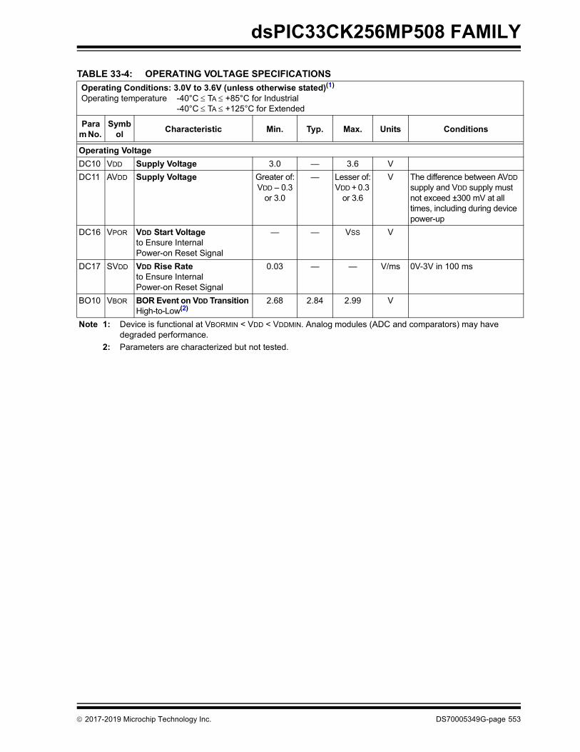
dsPIC33CK256MP508 FAMILY
TABLE 33-4: OPERATING VOLTAGE SPECIFICATIONSOperating Conditions: 3.0V to 3.6V (unless otherwise stated)(1)
Operating temperature -40°C TA +85°C for Industrial-40°C TA +125°C for Extended
Param No.
Symbol Characteristic Min. Typ. Max. Units Conditions
Operating VoltageDC10 VDD Supply Voltage 3.0 — 3.6 VDC11 AVDD Supply Voltage Greater of:
VDD – 0.3 or 3.0
— Lesser of:VDD + 0.3
or 3.6
V The difference between AVDD supply and VDD supply must not exceed ±300 mV at all times, including during device power-up
DC16 VPOR VDD Start Voltageto Ensure Internal Power-on Reset Signal
— — VSS V
DC17 SVDD VDD Rise Rateto Ensure InternalPower-on Reset Signal
0.03 — — V/ms 0V-3V in 100 ms
BO10 VBOR BOR Event on VDD Transition High-to-Low(2)
2.68 2.84 2.99 V
Note 1: Device is functional at VBORMIN < VDD < VDDMIN. Analog modules (ADC and comparators) may have degraded performance.
2: Parameters are characterized but not tested.
2017-2019 Microchip Technology Inc. DS70005349G-page 553

dsPIC33CK256MP508 FAMILY
TABLE 33-5: OPERATING CURRENT (IDD)(2)
Operating Conditions: 3.0V to 3.6V (unless otherwise stated)Operating temperature -40°C TA +85°C for Industrial
-40°C TA +125°C for Extended
Parameter No. Typ.(1) Max. Units Conditions DC20 7.76 10.7 mA -40°C
3.3V10 MIPS (N1 = 1, N2 = 5, N3 = 2,
M = 50, FVCO = 400 MHz, FPLLO = 40 MHz)
7.49 10 mA +25°C7.82 15.5 mA +85°C
10.32 23.5 mA +125°CDC21 10.36 13.1 mA -40°C
3.3V20 MIPS (N1 = 1, N2 = 5, N3 = 1,
M = 50, FVCO = 400 MHz, FPLLO = 80 MHz)
10.09 12.45 mA +25°C10.42 17.5 mA +85°C12.89 25.5 mA +125°C
DC22 14.54 17.45 mA -40°C
3.3V40 MIPS (N1 = 1, N2 = 3, N3 = 1,
M = 60, FVCO = 480 MHz, FPLLO = 160 MHz)
14.26 16.7 mA +25°C14.58 22 mA +85°C17.06 30 mA +125°C
DC23 22.2 25.4 mA -40°C
3.3V70 MIPS (N1 = 1, N2 = 2, N3 = 1,
M = 70, FVCO = 560 MHz, FPLLO = 280 MHz)
21.91 24.9 mA +25°C22.21 30.75 mA +85°C24.65 37.5 mA +125°C
DC24 27.36 30.7 mA -40°C
3.3V90 MIPS (N1 = 1, N2 = 2, N3 = 1,
M = 90, FVCO = 720 MHz, FPLLO = 360 MHz)
26.96 30.5 mA +25°C26.68 35 mA +85°C29.01 42 mA +125°C
DC25 27.14 30.9 mA -40°C
3.3V100 MIPS (N1 = 1, N2 = 1,
N3 = 1, M = 50, FVCO = 400 MHz, FPLLO = 400 MHz)
26.54 30.1 mA +25°C26.79 35 mA +85°C29.23 42.5 mA +125°C
Note 1: Data in the “Typ.” column are for design guidance only and are not tested.2: Base Run current (IDD) is measured as follows:
• Oscillator is switched to EC+PLL mode in software• OSC1 pin is driven with external 8 MHz square wave with levels from 0.3V to VDD – 0.3V• OSC2 is configured as an I/O in the Configuration Words (OSCIOFNC (FOSC[2]) = 0)• FSCM is disabled (FCKSM[1:0] (FOSC[7:6]) = 01)• Watchdog Timer is disabled (FWDT[15] = 0 and WDTCONL[15] = 0)• All I/O pins (except OSC1) are configured as outputs and driving low• No peripheral modules are operating or being clocked (defined PMDx bits are all ‘1’s)• JTAG is disabled (JTAGEN (FICD[5]) = 0)• NOP instructions are executed in while(1) loop
DS70005349G-page 554 2017-2019 Microchip Technology Inc.

dsPIC33CK256MP508 FAMILY
TABLE 33-6: IDLE CURRENT (IIDLE)(2) Operating Conditions: 3.0V to 3.6V (unless otherwise stated)Operating temperature -40°C TA +85°C for Industrial
-40°C TA +125°C for Extended
Parameter No. Typ.(1) Max. Units Conditions
DC40 6.41 8.47 mA -40°C
3.3V10 MIPS (N1 = 1, N2 = 5, N3 = 2,
M = 50, FVCO = 400 MHz, FPLLO = 40 MHz)
6.15 7.57 mA +25°C6.45 13 mA +85°C8.95 22 mA +125°C
DC41 7.31 10.1 mA -40°C
3.3V20 MIPS (N1 = 1, N2 = 5, N3 = 1,
M = 50, FVCO = 400 MHz, FPLLO = 80 MHz)
7.04 9.1 mA +25°C7.36 14.75 mA +85°C9.83 22.75 mA +125°C
DC42 9.4 12.3 mA -40°C
3.3V40 MIPS (N1 = 1, N2 = 3, N3 = 1,
M = 60, FVCO = 480 MHz, FPLLO = 160 MHz)
9.13 11.2 mA +25°C9.45 16.5 mA +85°C11.92 25 mA +125°C
DC43 12.39 15.3 mA -40°C
3.3V70 MIPS (N1 = 1, N2 = 2, N3 = 1,
M = 70, FVCO = 560 MHz, FPLLO = 280 MHz)
12.11 14.3 mA +25°C12.43 19.75 mA +85°C14.89 28.25 mA +125°C
DC44 14.78 17.85 mA -40°C
3.3V90 MIPS (N1 = 1, N2 = 2, N3 = 1,
M = 90, FVCO = 720 MHz, FPLLO = 360 MHz)
14.5 16.9 mA +25°C14.81 22.5 mA +85°C17.26 29.5 mA +125°C
DC45 14.44 17.55 mA -40°C
3.3V100 MIPS (N1 = 1, N2 = 1, N3 = 1,
M = 50, FVCO = 400 MHz, FPLLO = 400 MHz)
14.15 16.5 mA +25°C14.46 22.25 mA +85°C16.9 30 mA +125°C
Note 1: Data in the “Typ.” column are for design guidance only and are not tested.2: Base Idle current (IIDLE) is measured as follows:
• Oscillator is switched to EC+PLL mode in software• OSC1 pin is driven with external 8 MHz square wave with levels from 0.3V to VDD – 0.3V• OSC2 is configured as an I/O in the Configuration Words (OSCIOFNC (FOSC[2]) = 0)• FSCM is disabled (FCKSM[1:0] (FOSC[7:6]) = 01)• Watchdog Timer is disabled (FWDT[15] = 0 and WDTCONL[15] = 0)• All I/O pins (except OSC1) are configured as outputs and driving low• No peripheral modules are operating or being clocked (defined PMDx bits are all ‘1’s)• JTAG is disabled (JTAGEN (FICD[5]) = 0)• Flash in standby with NVMSIDL (NVMCON[12]) = 1
2017-2019 Microchip Technology Inc. DS70005349G-page 555

dsPIC33CK256MP508 FAMILY
TABLE 33-7: POWER-DOWN CURRENT (IPD)(2)
Operating Conditions: 3.0V to 3.6V (unless otherwise stated)Operating temperature -40°C TA +85°C for Industrial
-40°C TA +125°C for Extended
Parameter No. Characteristic Typ.(1) Max. Units Conditions
DC60 Base Power-Down Current 270 650 µA -40°C
3.3V418.99 1000 µA +25°C939.53 7250 µA +85°C
5.59 18.5 mA +125°C(3)
Note 1: Data in the “Typ.” column are for design guidance only and are not tested.2: Base Sleep current (IPD) is measured as follows:
• OSC1 pin is driven with external 8 MHz square wave with levels from 0.3V to VDD – 0.3V• OSC2 is configured as an I/O in the Configuration Words (OSCIOFNC (FOSC[2]) = 0)• FSCM is disabled (FCKSM[1:0] (FOSC[7:6]) = 01)• Watchdog Timer is disabled (FWDT[15] = 0 and WDTCONL[15] = 0)• All I/O pins (except OSC1) are configured as outputs and driving low• No peripheral modules are operating or being clocked (defined PMDx bits are all ‘1’s)• JTAG is disabled (JTAGEN (FICD[5]) = 0)• The regulators are in Standby mode (VREGS (RCON[8]) = 0• The regulators are in Low-Power mode (LPWREN (VREGCON[15]) = 1
3: The regulators are in High-Power mode (LPWREN (VREGCON[15]) = 0.
TABLE 33-8: DOZE CURRENT (IDOZE)Operating Conditions: 3.0V to 3.6V (unless otherwise stated)Operating temperature -40°C TA +85°C for Industrial
-40°C TA +125°C for Extended
Parameter No. Typ.(1) Max. Doze Ratio Units Conditions
DC70 18.19 20 1:2 mA-40°C
3.3V
70 MIPS (N = 1, N2 = 2, N3 = 1, M = 70,
FVCO = 560 MHz,FPLLO = 280 MHz)
12.66 15 1:128 mA17.54 20.15 1:2 mA
+25°C12.39 14.7 1:128 mA17.85 25 1:2 mA
+85°C12.7 20 1:128 mA
20.32 32.5 1:2 mA+125°C
15.17 28.5 1:128 mADC71 22.3 25.55 1:2 mA
-40°C
3.3V
100 MIPS (N = 1, N2 = 1, N3 = 1, M = 50,
FVCO = 400 MHz,FPLLO = 400 MHz)
14.83 17.25 1:128 mA21.86 25.05 1:2 mA
+25°C14.55 16.95 1:128 mA22.16 30 1:2 mA
+85°C14.86 22 1:128 mA24.62 36.5 1:2 mA
+125°C17.31 30 1:128 mA
Note 1: Data in the “Typ.” column are for design guidance only and are not tested.
DS70005349G-page 556 2017-2019 Microchip Technology Inc.

dsPIC33CK256MP508 FAMILY
TABLE 33-9: WATCHDOG TIMER DELTA CURRENT (IWDT)(1) Operating Conditions: 3.0V to 3.6V (unless otherwise stated)Operating temperature -40°C TA +85°C for Industrial
-40°C TA +125°C for Extended
Parameter No. Typ. Max. Units Conditions
DC61 0.75 5 µA -40°C
3.3V2.0 12 µA +25°C3.88 24 µA +85°C5.69 40 µA +125°C
Note 1: The IWDT current is the additional current consumed when the module is enabled. This current should be added to the base IPD current. All parameters are characterized but not tested during manufacturing.
TABLE 33-10: PWM DELTA CURRENT(1) Operating Conditions: 3.0V to 3.6V (unless otherwise stated)Operating temperature -40°C TA +85°C for Industrial
-40°C TA +125°C for Extended
Parameter No. Typ. Max. Units Conditions
DC100 5.96 6.6 mA -40°C
3.3V
PWM Output Frequency = 500 kHz,PWM Input (AFPLLO = 500 MHz)
(AVCO = 1000 MHz, PLLFBD = 125,APLLDIV1 = 2)
5.99 6.7 mA +25°C5.92 6.9 mA +85°C5.47 7 mA +125°C
DC101 4.89 5.4 mA -40°C
3.3V
PWM Output Frequency = 500 kHz,PWM Input (AFPLLO = 400 MHz),(AVCO = 400 MHz, PLLFBD = 50,
APLLDIV1 = 1)
4.91 5.5 mA +25°C4.85 5.7 mA +85°C4.42 5.7 mA +125°C
DC102 2.77 3.7 mA -40°C
3.3V
PWM Output Frequency = 500 kHz,PWM Input (AFPLLO = 200 MHz),(AVCO = 400 MHz, PLLFBD = 50,
APLLDIV1 = 2)
2.75 3.7 mA +25°C2.7 3.7 mA +85°C
2.26 3.7 mA +125°CDC103 1.67 2 mA -40°C
3.3V
PWM Output Frequency = 500 kHz,PWM Input (AFPLLO = 100 MHz),(AVCO = 400 MHz, PLLFBD = 50,
APLLDIV1 = 4)
1.66 2.2 mA +25°C1.63 2.3 mA +85°C1.17 2.3 mA +125°C
Note 1: APLL current is not included. The APLL current will be the same if more than one PWM is running. Listed delta currents are for only one PWM instance when HREN = 0 (PGxCONL[7]). All parameters are characterized but not tested during manufacturing.
2017-2019 Microchip Technology Inc. DS70005349G-page 557

dsPIC33CK256MP508 FAMILY
TABLE 33-11: APLL DELTA CURRENTOperating Conditions: 3.0V to 3.6V (unless otherwise stated)Operating temperature -40°C TA +85°C for Industrial
-40°C TA +125°C for Extended
Parameter No. Typ. Max. Units Conditions(1)
DC110 5.93 6.6 mA -40°C
3.3VAFPLLO = 500 MHz
(AVCO = 1000 MHz, PLLFBD = 125, APLLDIV1 = 2)
5.95 7 mA +25°C6.15 7.6 mA +85°C7.15 9 mA +125°C
DC111 2.72 3.3 mA -40°C
3.3VAFPLLO = 400 MHz
(AVCO = 400 MHz, PLLFBD = 50, APLLDIV1 = 1)
2.74 3.7 mA +25°C2.92 4.3 mA +85°C3.87 5.6 mA +125°C
DC112 1.39 2.7 mA -40°C
3.3VAFPLLO = 200 MHz
(AVCO = 400 MHz, PLLFBD = 50, APLLDIV1 = 2)
1.49 2.7 mA +25°C1.65 3 mA +85°C2.6 4.4 mA +125°C
DC113 0.79 1.1 mA -40°C
3.3VAFPLLO = 100 MHz
(AVCO = 400 MHz, PLLFBD = 50, APLLDIV1 = 4)
0.84 1.4 mA +25°C0.96 2.3 mA +85°C1.93 3.6 mA +125°C
Note 1: The APLL current will be the same if more than one PWM or DAC is run to the APLL clock. All parameters are characterized but not tested during manufacturing.
TABLE 33-12: ADC DELTA CURRENT(1) Operating Conditions: 3.0V to 3.6V (unless otherwise stated)Operating temperature -40°C TA +85°C for Industrial
-40°C TA +125°C for Extended
Parameter No. Typ. Max. Units Conditions
DC120 3.61 4 mA -40°C
3.3V TAD = 14.3 ns(3.5 Msps conversion rate)
3.68 4.1 mA +25°C3.69 4.2 mA +85°C3.89 4.6 mA +125°C
Note 1: Shared core continuous conversion. TAD = 14.3 nS (3.5 Msps conversion rate). Listed delta currents are for only one ADC core. All parameters are characterized but not tested during manufacturing.
DS70005349G-page 558 2017-2019 Microchip Technology Inc.

dsPIC33CK256MP508 FAMILY
TABLE 33-13: COMPARATOR + DAC DELTA CURRENTOperating Conditions: 3.0V to 3.6V (unless otherwise stated)Operating temperature -40°C TA +85°C for Industrial
-40°C TA +125°C for Extended
Parameter No. Typ. Max. Units Conditions
DC130 1.2 1.35 mA -40°C
3.3V AFPLLO @ 500 MHz(1)1.23 1.65 mA +25°C1.23 1.65 mA +85°C1.24 1.65 mA +125°C
Note 1: APLL current is not included. Listed delta currents are for only one comparator + DAC instance. All parameters are characterized but not tested during manufacturing.
TABLE 33-14: OP AMP DELTA CURRENT(1)
Operating Conditions: 3.0V to 3.6V (unless otherwise stated)Operating temperature -40°C TA +85°C for Industrial
-40°C TA +125°C for Extended
Parameter No. Typ. Max. Units Conditions
DC140 0.25 1 mA -40°C
3.3V0.27 1.1 mA +25°C0.32 1.4 mA +85°C0.46 1.7 mA +125°C
Note 1: Listed delta currents are for only one op amp instance. All parameters are characterized but not tested during manufacturing.
2017-2019 Microchip Technology Inc. DS70005349G-page 559

dsPIC33CK256MP508 FAMILY
DI20TABLE 33-15: I/O PIN INPUT SPECIFICATIONSOperating Conditions: 3.0V to 3.6V (unless otherwise stated)Operating temperature -40°C TA +85°C for Industrial
-40°C TA +125°C for Extended
Param No. Symbol Characteristic Min.(5) Typ.(1) Max.(6) Units Conditions
VIL Input Low VoltageDI10 Any I/O Pin and MCLR VSS — 0.2 VDD VDI18 I/O Pins with SDAx, SCLx VSS — 0.3 VDD V SMBus disabledDI19 I/O Pins with SDAx, SCLx VSS — 0.8 V SMBus enabledDI20 VIH Input High Voltage
I/O Pins Not 5V Tolerant(3) 0.8 VDD — VDD V5V Tolerant I/O Pins and MCLR(3) 0.8 VDD — 5.5 V5V Tolerant I/O Pins with SDAx, SCLx(3) 0.8 VDD — 5.5 V SMBus disabled5V Tolerant I/O Pins with SDAx, SCLx(3) 2.1 — 5.5 V SMBus enabledI/O Pins with SDAx, SCLx Not 5V Tolerant(3)
0.8 VDD — VDD V SMBus disabled
I/O Pins with SDAx, SCLx Not 5V Tolerant(3)
2.1 — VDD V SMBus enabled
DI30 ICNPU Input Change Notification Pull-up Current(2,4)
175 360 545 µA VDD = 3.6V, VPIN = VSS
DI31 ICNPD Input Change Notification Pull-Down Current(4)
65 215 360 µA VDD = 3.6V, VPIN = VDD
DI50 IIL Input Leakage Current(2)
I/O Pins 5V Tolerant(3) -700 — 700 nAI/O Pins Not 5V Tolerant(3) -700 — 700 nAMCLR -700 — 700 nAOSCI -700 — 700 nA XT and HS modes
Note 1: Data in the “Typ.” column are at 3.3V, +25°C unless otherwise stated.2: Negative current is defined as current sourced by the pin.3: See the “Pin Diagrams” section for the 5V tolerant I/O pins.4: Characterized but not tested.5: VPIN = VSS.6: VPIN = VDD.
DS70005349G-page 560 2017-2019 Microchip Technology Inc.

dsPIC33CK256MP508 FAMILY
TABLE 33-16: I/O PIN INPUT INJECTION CURRENT SPECIFICATIONSOperating Conditions: 3.0V to 3.6V (unless otherwise stated)Operating temperature -40°C TA +85°C for Industrial
-40°C TA +125°C for Extended
Param No. Symbol Characteristic Min. Max. Units Conditions
DI60a IICL Input Low Injection Current 0 -5(1,4) mA All pinsDI60b IICH Input High Injection Current 0 +5(2,3,4) mA All pins, excepting all 5V tolerant
pins and SOSCIDI60c IICT Total Input Injection Current (sum of
all I/O and control pins)(5)-20 +20 mA Absolute instantaneous sum of all
± input injection currents from all I/O pins( | IICL | + | IICH | ) IICT
Note 1: VIL Source < (VSS – 0.3).2: VIH Source > (VDD + 0.3) for non-5V tolerant pins only.3: 5V tolerant pins do not have an internal high-side diode to VDD, and therefore, cannot tolerate any
“positive” input injection current.4: Injection currents can affect the ADC results.5: Any number and/or combination of I/O pins, not excluded under IICL or IICH conditions, are permitted in the sum.
TABLE 33-17: I/O PIN OUTPUT SPECIFICATIONSOperating Conditions: 3.0V to 3.6V (unless otherwise stated)Operating temperature -40°C TA +85°C for Industrial
-40°C TA +125°C for Extended
Param. Symbol Characteristic Min. Typ. Max. Units Conditions
DO10 VOL Output Low Voltage4x Sink Driver Pins
— — 0.42 V VDD = 3.6V, IOL < 9 mA
Output Low Voltage8x Sink Driver Pins(1)
— — 0.4 V VDD = 3.6V, IOL < 11 mA
DO20 VOH Output High Voltage4x Source Driver Pins
2.4 — — V VDD = 3.6V, IOH > -8 mA
Output High Voltage8x Source Driver Pins(1)
2.4 — — V VDD = 3.6V, IOH > -12 mA
Note 1: The 8x sink/source pins are RB1, RC8, RC9 and RD8.
2017-2019 Microchip Technology Inc. DS70005349G-page 561

dsPIC33CK256MP508 FAMILY
TABLE 33-18: PROGRAM MEMORYOperating Conditions: 3.0V to 3.6V (unless otherwise stated)Operating temperature -40°C TA +85°C for Industrial
-40°C TA +125°C for Extended
ParamNo. Symbol Characteristic Min. Max. Units Conditions
Program Flash MemoryD130 EP Cell Endurance 10,000 — E/W -40C to +125CD131 VPR VDD for Read 3.0 3.6 VD132b VPEW VDD for Self-Timed Write 3.0 3.6 VD134 TRETD Characteristic Retention 20 — Year Provided no other specifications are
violated, -40C to +125CD137a TPE Page Erase Time 15.3 16.82 ms TPE = 128,454 FRC cycles (Note 1)D138a TWW Word Write Time 47.7 52.3 µs TWW = 400 FRC cycles (Note 1)D139a TRW Row Write Time 2.0 2.2 ms TRW = 16,782 FRC cycles (Note 1)Note 1: Other conditions: FRC = 8 MHz, TUN[5:0] = 011111 (for Minimum), TUN[5:0] = 100000 (for Maximum).
This parameter depends on the FRC accuracy (see Table 33-22) and the value of the FRC Oscillator Tuning register (see Register 9-4). For complete details on calculating the Minimum and Maximum time, see Section 5.3 “Programming Operations”.
DS70005349G-page 562 2017-2019 Microchip Technology Inc.

dsPIC33CK256MP508 FAMILY
33.2 AC Characteristics and Timing Parameters
FIGURE 33-1: LOAD CONDITIONS FOR I/O SPECIFICATIONS
VDD/2
CL
RL
Pin
VSS
RL = 464CL = 50 pF
2017-2019 Microchip Technology Inc. DS70005349G-page 563

dsPIC33CK256MP508 FAMILY
FIGURE 33-2: EXTERNAL CLOCK TIMING
OSCI
CLKO
OS20OS30 OS30
OS40OS41
OS31OS25
OS31
TABLE 33-19: EXTERNAL CLOCK TIMING REQUIREMENTS Operating Conditions: 3.0V to 3.6V (unless otherwise stated)Operating temperature -40°C TA +85°C for Industrial
-40°C TA +125°C for Extended
ParamNo. Sym Characteristic Min. Typ.(1) Max. Units Conditions
OS10 FIN External CLKI Frequency DC — 64 MHzOscillator Crystal Frequency 3.5 — 10 MHz XT
10 — 32 MHz HSOS20 TOSCI External Clock Period 15.63 — DC nsOS25 TCY Instruction Cycle Time 10 — DC nsOS30 TosL,
TosHExternal Clock in (OSCI)High or Low Time
0.45 x TOSC — 0.55 x TOSC ns
OS31 TosR,TosF
External Clock in (OSCI)Rise or Fall Time
— — 5.2 ns When FIN = 64 MHz
OS40 TckR CLKO Rise Time(2,3) — 5.4 — nsOS41 TckF CLKO Fall Time(2,3) — 6.4 — nsOS42 GM External Oscillator
Transconductance(3)2.7 — 4 mA/V XTCFG[1:0] = 00,
XTBST = 04 — 7 mA/V XTCFG[1:0] = 00,
XTBST = 14.5 — 7 mA/V XTCFG[1:0] = 01,
XTBST = 06 — 11.9 mA/V XTCFG[1:0] = 01,
XTBST = 15.9 — 9.7 mA/V XTCFG[1:0] = 10,
XTBST = 06.9 — 15.9 mA/V XTCFG[1:0] = 10,
XTBST = 16.7 — 12 mA/V XTCFG[1:0] = 11,
XTBST = 07.5 — 19 mA/V XTCFG[1:0] = 11,
XTBST = 1Note 1: Data in the “Typ.” column are at 3.3V, +25°C unless otherwise stated.
2: Measurements are taken in EC mode. The CLKO signal is measured on the OSCO pin. 3: This parameter is characterized but not tested in manufacturing.
DS70005349G-page 564 2017-2019 Microchip Technology Inc.

dsPIC33CK256MP508 FAMILY
TABLE 33-20: PLL TIMING SPECIFICATIONSOperating Conditions: 3.0V to 3.6V (unless otherwise stated)Operating temperature -40°C TA +85°C for Industrial
-40°C TA +125°C for Extended
ParamNo. Symbol Characteristic Min. Typ.(1) Max. Units Conditions
OS50 FPLLI PLL Voltage Controlled Oscillator (VCO) Input Frequency Range
8(2) — 64 MHz ECPLL, XTPLL modes
OS51 FVCO On-Chip VCO System Frequency 400 — 1600 MHzOS52 TLOCK PLL Start-up Time (Lock Time) — 125 — µsNote 1: Data in the “Typ.” column are at 3.3V, +25°C unless otherwise stated. Parameters are for design guidance
only and are not tested.2: Inclusive of FRC Tolerance Specification F20a.
TABLE 33-21: AUXILIARY PLL TIMING SPECIFICATIONSOperating Conditions: 3.0V to 3.6V (unless otherwise stated)Operating temperature -40°C TA +85°C for Industrial
-40°C TA +125°C for Extended
ParamNo. Symbol Characteristic Min. Typ.(1) Max. Units Conditions
OS50 AFPLLI APLL Voltage Controlled Oscillator (VCO) Input Frequency Range
8(2) — 64 MHz ECPLL, XTPLL modes
OS51 AFVCO On-Chip VCO System Frequency 400 — 1600 MHzOS52 TLOCK APLL Start-up Time (Lock Time) — 125 — µsNote 1: Data in the “Typ.” column are at 3.3V, +25°C unless otherwise stated. Parameters are for design guidance
only and are not tested.2: Inclusive of FRC Tolerance Specification F20a.
2017-2019 Microchip Technology Inc. DS70005349G-page 565

dsPIC33CK256MP508 FAMILY
TABLE 33-22: INTERNAL FRC ACCURACYOperating Conditions: 3.0V to 3.6V (unless otherwise stated)Operating temperature -40°C TA +85°C for Industrial
-40°C TA +125°C for Extended
Param No. Characteristic Min. Max. Units Conditions
Internal FRC Accuracy @ FRC Frequency = 8 MHz(1)
F20a FRC -3 +3 % -40°C TA 0°C-1.5 +1.5 % 0°C TA +85°C-2 +2 % +85°C TA +125°C
F22 BFRC -17 +17 % -40°C TA +125°CNote 1: Frequency is calibrated at +25°C and 3.3V.
TABLE 33-23: INTERNAL LPRC ACCURACYOperating Conditions: 3.0V to 3.6V (unless otherwise stated)Operating temperature -40°C TA +85°C for Industrial
-40°C TA +125°C for Extended
ParamNo. Characteristic Min. Max. Units Conditions
LPRC @ 32 kHzF21 LPRC -25 +25 % -40°C TA 0°C
-10 +10 % 0°C TA +85°C-15 +15 % +85°C TA +125°C
DS70005349G-page 566 2017-2019 Microchip Technology Inc.

dsPIC33CK256MP508 FAMILY
FIGURE 33-3: I/O TIMING CHARACTERISTICS
FIGURE 33-4: BOR AND MASTER CLEAR RESET TIMING CHARACTERISTICS
Note: Refer to Figure 33-1 for load conditions.
I/O Pin(Input)
I/O Pin(Output)
DI35
Old Value New Value
DI40
DO31DO32
TABLE 33-24: I/O TIMING REQUIREMENTSOperating Conditions: 3.0V to 3.6V (unless otherwise stated)Operating temperature -40°C TA +85°C for Industrial
-40°C TA +125°C for Extended
ParamNo. Symbol Characteristic Min. Typ.(1) Max. Units Conditions
DO31 TIOR Port Output Rise Time(2) — 6.5 9.7 nsDO32 TIOF Port Output Fall Time(2) — 3.2 4.2 nsDI35 TINP INTx Pin High or Low Time (input) 20 — — nsDI40 TRBP CNx High or Low Time (input) 2 — — TCY
Note 1: Data in the “Typ.” column are at 3.3V, +25°C unless otherwise stated.2: This parameter is characterized but not tested in manufacturing.
MCLR
(SY20)
BOR
(SY30)
TMCLR
TBOR
Reset Sequence
CPU Starts Fetching Code
Various Delays (depending on configuration)
2017-2019 Microchip Technology Inc. DS70005349G-page 567

dsPIC33CK256MP508 FAMILY
TABLE 33-25: RESET, WATCHDOG TIMER, OSCILLATOR START-UP TIMER, POWER-UP TIMER TIMING REQUIREMENTS
Operating Conditions: 3.0V to 3.6V (unless otherwise stated)Operating temperature -40°C TA +85°C for Industrial
-40°C TA +125°C for Extended
ParamNo. Symbol Characteristic(1) Min. Typ.(2) Max. Units Conditions
SY00 TPU Power-up Period — 200 — µs FNOSC[2:0] are FRCSY10 TOST Oscillator Start-up Time — 1024 TOSC — — TOSC = OSCI periodSY13 TIOZ I/O High-Impedance
from MCLR Low or Watchdog Timer Reset
— 1.5 — µs
SY20 TMCLR MCLR Pulse Width (low) 2 — — µsSY30 TBOR BOR Pulse Width (low) 1 — — µsSY35 TFSCM Fail-Safe Clock Monitor
Delay— — 40 µs Clock fail to BFRC switch
SY37 TOSCDFRC FRC Oscillator Start-up Delay
— — 15 µs From POR event
SY38 TOSCDLPRC LPRC Oscillator Start-up Delay
— — 50 µs From Reset event
Note 1: These parameters are characterized but not tested in manufacturing.2: Data in the “Typ.” column are at 3.3V, +25°C unless otherwise stated.
DS70005349G-page 568 2017-2019 Microchip Technology Inc.

dsPIC33CK256MP508 FAMILY
FIGURE 33-5: HIGH-SPEED PWMx MODULE FAULT TIMING CHARACTERISTICS
FIGURE 33-6: HIGH-SPEED PWMx MODULE TIMING CHARACTERISTICS
Fault Input
PWMx
MP30
MP20(active-low)
PWMx
MP11 MP10
Note: Refer to Figure 33-1 for load conditions.
TABLE 33-26: HIGH-SPEED PWMx MODULE TIMING REQUIREMENTSOperating Conditions: 3.0V to 3.6V (unless otherwise stated)Operating temperature -40°C TA +85°C for Industrial
-40°C TA +125°C for Extended
ParamNo. Symbol Characteristic(1) Min. Max. Units Conditions
MP00 FIN PWM Input Frequency — 500 MHz (Note 2)MP10 TFPWM PWMx Output Fall Time — — ns See Parameter DO32MP11 TRPWM PWMx Output Rise Time — — ns See Parameter DO31MP20 TFD Fault Input to PWMx I/O Change — 26 ns PCI Inputs 19 through 22MP30 TFH Fault Input Pulse Width 8 — nsNote 1: These parameters are characterized but not tested in manufacturing.
2: Input frequency of 500 MHz must be used for High-Resolution mode.
2017-2019 Microchip Technology Inc. DS70005349G-page 569

dsPIC33CK256MP508 FAMILY
TABLE 33-27: SPIx MAXIMUM DATA/CLOCK RATE SUMMARY
FIGURE 33-7: SPIx MASTER MODE (HALF-DUPLEX, TRANSMIT ONLY, CKE = 0) TIMING CHARACTERISTICS
SPI Master Transmit Only (Half-Duplex)
SPI Master Transmit/Receive
(Full-Duplex)
SPI Slave Transmit/Receive
(Full-Duplex)CKE
Figure 33-7Table 33-28 — — 0
Figure 33-8Table 33-28 — — 1
— Figure 33-9Table 33-29 — 0
— Figure 33-10Table 33-30 — 1
— — Figure 33-11Table 33-32 0
— — Figure 33-12Table 33-33 1
SCKx(CKP = 0)
SCKx(CKP = 1)
SDOx
SP10
SP21SP20SP35
SP20SP21
MSb LSbBit 14 - - - - - -1
SP30, SP31SP30, SP31
Note: Refer to Figure 33-1 for load conditions.
DS70005349G-page 570 2017-2019 Microchip Technology Inc.

dsPIC33CK256MP508 FAMILY
FIGURE 33-8: SPIx MASTER MODE (HALF-DUPLEX, TRANSMIT ONLY, CKE = 1) TIMING CHARACTERISTICS
TABLE 33-28: SPIx MASTER MODE (HALF-DUPLEX, TRANSMIT ONLY) TIMING REQUIREMENTSOperating Conditions: 3.0V to 3.6V (unless otherwise stated)Operating temperature -40°C TA +85°C for Industrial
-40°C TA +125°C for Extended
ParamNo. Symbol Characteristic(1) Min. Typ.(2) Max. Units Conditions
SP10 FscP Maximum SCKx Frequency — — 15 MHz Using PPS pins— — 40 MHz SPIx dedicated pins
SP20 TscF SCKx Output Fall Time — — — ns See Parameter DO32SP21 TscR SCKx Output Rise Time — — — ns See Parameter DO31SP30 TdoF SDOx Data Output Fall Time — — — ns See Parameter DO32SP31 TdoR SDOx Data Output Rise Time — — — ns See Parameter DO31SP35 TscH2doV,
TscL2doVSDOx Data Output Valid After SCKx Edge
— 6 20 ns
SP36 TdiV2scH,TdiV2scL
SDOx Data Output Setup to First SCKx Edge
30 — — ns Using PPS pins3 — — ns SPIx dedicated pins
Note 1: These parameters are characterized but not tested in manufacturing.2: Data in the “Typ.” column are at 3.3V, +25°C unless otherwise stated.
SCKx(CKP = 0)
SCKx(CKP = 1)
SDOx
SP21SP20SP35
SP20SP21
MSb LSbBit 14 - - - - - -1
SP30, SP31
Note: Refer to Figure 33-1 for load conditions.
SP36
SP10
2017-2019 Microchip Technology Inc. DS70005349G-page 571

dsPIC33CK256MP508 FAMILY
FIGURE 33-9: SPIx MASTER MODE (FULL-DUPLEX, CKE = 1, CKP = x, SMP = 1) TIMING CHARACTERISTICS
TABLE 33-29: SPIx MASTER MODE (FULL-DUPLEX, CKE = 1, CKP = x, SMP = 1) TIMING REQUIREMENTS
Operating Conditions: 3.0V to 3.6V (unless otherwise stated)Operating temperature -40°C TA +85°C for Industrial
-40°C TA +125°C for Extended
ParamNo. Symbol Characteristic(1) Min. Typ.(2) Max. Units Conditions
SP10 FscP Maximum SCKx Frequency — — 15 MHz Using PPS pins— — 40 MHz SPIx dedicated pins
SP20 TscF SCKx Output Fall Time — — — ns See Parameter DO32SP21 TscR SCKx Output Rise Time — — — ns See Parameter DO31SP30 TdoF SDOx Data Output Fall
Time— — — ns See Parameter DO32
SP31 TdoR SDOx Data Output Rise Time
— — — ns See Parameter DO31
SP35 TscH2doV,TscL2doV
SDOx Data Output Valid After SCKx Edge
— 6 20 ns
SP36 TdoV2sc, TdoV2scL
SDOx Data Output Setup to First SCKx Edge
30 — — ns Using PPS pins3 — — ns SPIx dedicated pins
SP40 TdiV2scH, TdiV2scL
Setup Time of SDIx Data Input to SCKx Edge
30 — — ns Using PPS pins10 — — ns SPIx dedicated pins
SP41 TscH2diL, TscL2diL
Hold Time of SDIx Data Input to SCKx Edge
30 — — ns Using PPS pins15 — — ns SPIx dedicated pins
Note 1: These parameters are characterized but not tested in manufacturing.2: Data in the “Typ.” column are at 3.3V, +25°C unless otherwise stated.
SCKx(CKP = 0)
SCKx(CKP = 1)
SDOx
SP21SP20SP35
SP20SP21
MSb LSbBit 14 - - - - - -1
SP30, SP31
Note: Refer to Figure 33-1 for load conditions.
SP36
SP41
LSb InBit 14 - - - -1SDIx
SP40
SP10
MSb In
DS70005349G-page 572 2017-2019 Microchip Technology Inc.

dsPIC33CK256MP508 FAMILY
FIGURE 33-10: SPIx MASTER MODE (FULL-DUPLEX, CKE = 0, CKP = x, SMP = 1) TIMING CHARACTERISTICS
TABLE 33-30: SPIx MASTER MODE (FULL-DUPLEX, CKE = 0, CKP = x, SMP = 1) TIMING REQUIREMENTS
Operating Conditions: 3.0V to 3.6V (unless otherwise stated)Operating temperature -40°C TA +85°C for Industrial
-40°C TA +125°C for ExtendedParam
No. Symbol Characteristic(1) Min. Typ.(2) Max. Units Conditions
SP10 FscP Maximum SCKx Frequency — — 15 MHz Using PPS pins — — 40 MHz SPIx dedicated pins
SP20 TscF SCKx Output Fall Time — — — ns See Parameter DO32SP21 TscR SCKx Output Rise Time — — — ns See Parameter DO31SP30 TdoF SDOx Data Output Fall Time — — — ns See Parameter DO32SP31 TdoR SDOx Data Output Rise Time — — — ns See Parameter DO31SP35 TscH2doV,
TscL2doVSDOx Data Output Valid AfterSCKx Edge
— 6 20 ns
SP36 TdoV2scH, TdoV2scL
SDOx Data Output Setup toFirst SCKx Edge
30 — — ns Using PPS pins20 — — ns SPIx dedicated pins
SP40 TdiV2scH, TdiV2scL
Setup Time of SDIx Data Input to SCKx Edge
30 — — ns Using PPS pins10 — — ns SPIx dedicated pins
SP41 TscH2diL, TscL2diL
Hold Time of SDIx Data Inputto SCKx Edge
30 — — ns Using PPS pins15 — — ns SPIx dedicated pins
Note 1: These parameters are characterized but not tested in manufacturing.2: Data in the “Typ.” column are at 3.3V, +25°C unless otherwise stated.
SCKx(CKP = 0)
SCKx(CKP = 1)
SDOx
SDIx
SP40 SP41
SP21SP20SP35
SP20SP21
MSb LSbBit 14 - - - - - -1
LSb InBit 14 - - - -1
SP30, SP31SP30, SP31
SP36
SP10
MSb In
Note: Refer to Figure 33-1 for load conditions.
2017-2019 Microchip Technology Inc. DS70005349G-page 573

dsPIC33CK256MP508 FAMILY
FIGURE 33-11: SPIx SLAVE MODE (FULL-DUPLEX, CKE = 0, CKP = x, SMP = 0) TIMING CHARACTERISTICS
SSx
SCKx(CKP = 0)
SCKx(CKP = 1)
SDOx
SP50
SP40
SP41
SP30, SP31 SP51
SP35
MSb LSbBit 14 - - - - - -1
Bit 14 - - - -1 LSb In
SP52
SP73SP72
SP72SP73
Note: Refer to Figure 33-1 for load conditions.
SDIx
SP10
SP36
MSb In
DS70005349G-page 574 2017-2019 Microchip Technology Inc.

dsPIC33CK256MP508 FAMILY
TABLE 33-31: SPIx SLAVE MODE (FULL-DUPLEX, CKE = 0, CKP = x, SMP = 0) TIMING REQUIREMENTS
Operating Conditions: 3.0V to 3.6V (unless otherwise stated)Operating temperature -40°C TA +85°C for Industrial
-40°C TA +125°C for Extended
ParamNo. Symbol Characteristic(1) Min. Typ.(2) Max. Units Conditions
SP10 FscP Maximum SCKx Input Frequency — — 15 MHz Using PPS pins— — 40 MHz SPIx dedicated pins
SP72 TscF SCKx Input Fall Time — — — ns See Parameter DO32 SP73 TscR SCKx Input Rise Time — — — ns See Parameter DO31 SP30 TdoF SDOx Data Output Fall Time — — — ns See Parameter DO32SP31 TdoR SDOx Data Output Rise Time — — — ns See Parameter DO31SP35 TscH2doV,
TscL2doVSDOx Data Output Valid AfterSCKx Edge
— 6 20 ns
SP36 TdoV2scH, TdoV2scL
SDOx Data Output Setup toFirst SCKx Edge
30 — — ns Using PPS pins20 — — ns SPIx dedicated pins
SP40 TdiV2scH, TdiV2scL
Setup Time of SDIx Data Inputto SCKx Edge
30 — — ns Using PPS pins10 — — ns SPIx dedicated pins
SP41 TscH2diL, TscL2diL
Hold Time of SDIx Data Inputto SCKx Edge
30 — — ns Using PPS pins15 — — ns SPIx dedicated pins
SP50 TssL2scH, TssL2scL
SSx to SCKx or SCKx Input
120 — — ns
SP51 TssH2doZ SSx to SDOx OutputHigh-Impedance
8 — 50 ns
SP52 TscH2ssH,TscL2ssH
SSx After SCKx Edge 1.5 TCY + 40 — — ns
Note 1: These parameters are characterized but not tested in manufacturing.2: Data in the “Typ.” column are at 3.3V, +25°C unless otherwise stated.
2017-2019 Microchip Technology Inc. DS70005349G-page 575

dsPIC33CK256MP508 FAMILY
FIGURE 33-12: SPIx SLAVE MODE (FULL-DUPLEX, CKE = 1, CKP = x, SMP = 0) TIMING CHARACTERISTICS
SSx
SCKx(CKP = 0)
SCKx(CKP = 1)
SDOx
SP60
SDIx
SP30, SP31
MSb Bit 14 - - - - - -1 LSb
SP51
Bit 14 - - - -1 LSb In
SP52
SP73SP72
SP72SP73
SP40
SP41
Note: Refer to Figure 33-1 for load conditions.
SP36
SP50
SP10
SP35
MSb In
DS70005349G-page 576 2017-2019 Microchip Technology Inc.

dsPIC33CK256MP508 FAMILY
TABLE 33-32: SPIx SLAVE MODE (FULL-DUPLEX, CKE = 1, CKP = x, SMP = 0) TIMING REQUIREMENTS
Operating Conditions: 3.0V to 3.6V (unless otherwise stated)Operating temperature -40°C TA +85°C for Industrial
-40°C TA +125°C for Extended
ParamNo. Symbol Characteristic(1) Min. Typ.(2) Max. Units Conditions
SP10 FscP Maximum SCKx Input Frequency
— — 15 MHz Using PPS pins — — 40 MHz SPIx dedicated pins
SP72 TscF SCKx Input Fall Time — — — ns See Parameter DO32SP73 TscR SCKx Input Rise Time — — — ns See Parameter DO31SP30 TdoF SDOx Data Output Fall Time — — — ns See Parameter DO32SP31 TdoR SDOx Data Output Rise Time — — — ns See Parameter DO31SP35 TscH2doV,
TscL2doVSDOx Data Output Valid AfterSCKx Edge
— 6 20 ns
SP36 TdoV2scH, TdoV2scL
SDOx Data Output Setup toFirst SCKx Edge
30 — — ns Using PPS pins20 — — ns SPIx dedicated pins
SP40 TdiV2scH, TdiV2scL
Setup Time of SDIx Data Inputto SCKx Edge
30 — — ns Using PPS pins10 — — ns SPIx dedicated pins
SP41 TscH2diL, TscL2diL
Hold Time of SDIx Data Inputto SCKx Edge
30 — — ns Using PPS pins15 — — ns SPIx dedicated pins
SP50 TssL2scH, TssL2scL
SSx to SCKx or SCKx Input
120 — — ns
SP51 TssH2doZ SSx to SDOx OutputHigh-Impedance
8 — 50 ns
SP52 TscH2ssH,TscL2ssH
SSx After SCKx Edge 1.5 TCY + 40 — — ns
SP60 TssL2doV SDOx Data Output Valid After SSx Edge
— — 50 ns
Note 1: These parameters are characterized but not tested in manufacturing.2: Data in the “Typ.” column are at 3.3V, +25°C unless otherwise stated.
2017-2019 Microchip Technology Inc. DS70005349G-page 577

dsPIC33CK256MP508 FAMILY
FIGURE 33-13: I2Cx BUS START/STOP BITS TIMING CHARACTERISTICS (MASTER MODE)
FIGURE 33-14: I2Cx BUS DATA TIMING CHARACTERISTICS (MASTER MODE)
SCLx
SDAx
StartCondition
StopCondition
Note: Refer to Figure 33-1 for load conditions.
IM31
IM30
IM34
IM33
IM11IM10 IM33
IM11IM10
IM20
IM25
IM40 IM40 IM45
IM21
SCLx
SDAxIn
SDAxOut
Note: Refer to Figure 33-1 for load conditions.
IM26
DS70005349G-page 578 2017-2019 Microchip Technology Inc.

dsPIC33CK256MP508 FAMILY
TABLE 33-33: I2Cx BUS DATA TIMING REQUIREMENTS (MASTER MODE)Operating Conditions: 3.0V to 3.6V (unless otherwise stated)Operating temperature -40°C TA +85°C for Industrial
-40°C TA +125°C for Extended Param
No. Symbol Characteristic(4) Min.(1) Max. Units Conditions
IM10 TLO:SCL Clock Low Time 100 kHz mode TCY (BRG + 1) — µs400 kHz mode TCY (BRG + 1) — µs1 MHz mode(2) TCY (BRG + 1) — µs
IM11 THI:SCL Clock High Time 100 kHz mode TCY (BRG + 1) — µs400 kHz mode TCY (BRG + 1) — µs1 MHz mode(2) TCY (BRG + 1) — µs
IM20 TF:SCL SDAx and SCLxFall Time
100 kHz mode — 300 ns CB is specified to be from 10 to 400 pF400 kHz mode 20 x (VDD/5.5V) 300 ns
1 MHz mode(2) 20 x (VDD/5.5V) 120 nsIM21 TR:SCL SDAx and SCLx
Rise Time100 kHz mode — 1000 ns CB is specified to be
from 10 to 400 pF400 kHz mode 20 + 0.1 CB 300 ns1 MHz mode(2) — 120 ns
IM25 TSU:DAT Data InputSetup Time
100 kHz mode 250 — ns400 kHz mode 100 — ns1 MHz mode(2) 50 — ns
IM26 THD:DAT Data InputHold Time
100 kHz mode 0 — µs400 kHz mode 0 0.9 µs1 MHz mode(2) 0 0.3 µs
IM30 TSU:STA Start ConditionSetup Time
100 kHz mode TCY (BRG + 1) — µs Only relevant for Repeated Startcondition
400 kHz mode TCY (BRG + 1) — µs1 MHz mode(2) TCY (BRG + 1) — µs
IM31 THD:STA Start Condition Hold Time
100 kHz mode TCY (BRG + 1) — µs After this period, thefirst clock pulse isgenerated
400 kHz mode TCY (BRG + 1) — µs1 MHz mode(2) TCY (BRG + 1) — µs
IM33 TSU:STO Stop Condition Setup Time
100 kHz mode TCY (BRG + 1) — µs400 kHz mode TCY (BRG + 1) — µs1 MHz mode(2) TCY (BRG + 1) — µs
IM34 THD:STO Stop ConditionHold Time
100 kHz mode TCY (BRG + 1) — µs400 kHz mode TCY (BRG + 1) — µs1 MHz mode(2) TCY (BRG + 1) — µs
IM40 TAA:SCL Output Valid from Clock
100 kHz mode — 3450 ns400 kHz mode — 900 ns1 MHz mode(2) — 450 ns
IM45 TBF:SDA Bus Free Time 100 kHz mode 4.7 — µs Time the bus must be free before a newtransmission can start
400 kHz mode 1.3 — µs1 MHz mode(2) 0.5 — µs
IM50 CB Bus Capacitive Loading — 400 pF IM51 TPGD Pulse Gobbler Delay 65 390 ns (Note 3)Note 1: BRG is the value of the I2C Baud Rate Generator.
2: Maximum Pin Capacitance = 10 pF for all I2Cx pins (for 1 MHz mode only).3: Typical value for this parameter is 130 ns.4: These parameters are characterized but not tested in manufacturing.
2017-2019 Microchip Technology Inc. DS70005349G-page 579

dsPIC33CK256MP508 FAMILY
FIGURE 33-15: I2Cx BUS START/STOP BITS TIMING CHARACTERISTICS (SLAVE MODE)
FIGURE 33-16: I2Cx BUS DATA TIMING CHARACTERISTICS (SLAVE MODE)
SCLx
SDAx
StartCondition
StopCondition
IS30
IS31 IS34
IS33
IS30IS31 IS33
IS11
IS10
IS20
IS25
IS40 IS40 IS45
IS21
SCLx
SDAxIn
SDAxOut
IS26
DS70005349G-page 580 2017-2019 Microchip Technology Inc.

dsPIC33CK256MP508 FAMILY
TABLE 33-34: I2Cx BUS DATA TIMING REQUIREMENTS (SLAVE MODE)Operating Conditions: 3.0V to 3.6V (unless otherwise stated)Operating temperature -40°C TA +85°C for Industrial
-40°C TA +125°C for ExtendedParam
No. Symbol Characteristic(3) Min. Max. Units Conditions
IS10 TLO:SCL Clock Low Time 100 kHz mode 4.7 — µs400 kHz mode 1.3 — µs1 MHz mode(1) 0.5 — µs
IS11 THI:SCL Clock High Time 100 kHz mode 4.0 — µs Device must operate at a minimum of 1.5 MHz
400 kHz mode 0.6 — µs Device must operate at a minimum of 10 MHz
1 MHz mode(1) 0.26 — µsIS20 TF:SCL SDAx and SCLx
Fall Time100 kHz mode — 300 ns CB is specified to be from
10 to 400 pF400 kHz mode 20 x (VDD/5.5V) 300 ns1 MHz mode(1) 20 x (VDD/5.5V) 120 ns
IS21 TR:SCL SDAx and SCLxRise Time
100 kHz mode — 1000 ns CB is specified to be from10 to 400 pF400 kHz mode 20 + 0.1 CB 300 ns
1 MHz mode(1) — 120 nsIS25 TSU:DAT Data Input
Setup Time100 kHz mode 250 — ns400 kHz mode 100 — ns1 MHz mode(1) 50 — ns
IS26 THD:DAT Data InputHold Time
100 kHz mode 0 — µs400 kHz mode 0 0.9 µs1 MHz mode(1) 0 0.3 µs
IS30 TSU:STA Start ConditionSetup Time
100 kHz mode 4.7 — µs Only relevant for Repeated Start condition400 kHz mode 0.6 — µs
1 MHz mode(1) 0.26 — µsIS31 THD:STA Start Condition
Hold Time 100 kHz mode 4.0 — µs After this period, the first
clock pulse is generated400 kHz mode 0.6 — µs1 MHz mode(1) 0.26 — µs
IS33 TSU:STO Stop Condition Setup Time
100 kHz mode 4.0 — µs400 kHz mode 0.6 — µs1 MHz mode(1) 0.26 — µs
IS34 THD:STO Stop ConditionHold Time
100 kHz mode >0 — µs400 kHz mode >0 — µs1 MHz mode(1) >0 µs
IS40 TAA:SCL Output Valid from Clock
100 kHz mode 0 3450 ns400 kHz mode 0 900 ns1 MHz mode(1) 0 450 ns
IS45 TBF:SDA Bus Free Time 100 kHz mode 4.7 — µs Time the bus must be free before a new transmission can start
400 kHz mode 1.3 — µs1 MHz mode(1) 0.5 — µs
IS50 CB Bus Capacitive Loading — 400 pF IS51 TPGD Pulse Gobbler Delay 65 390 ns (Note 2)Note 1: Maximum Pin Capacitance = 10 pF for all I2Cx pins (for 1 MHz mode only).
2: Typical value for this parameter is 130 ns.3: These parameters are characterized but not tested in manufacturing.
2017-2019 Microchip Technology Inc. DS70005349G-page 581

dsPIC33CK256MP508 FAMILY
FIGURE 33-17: UARTx MODULE I/O TIMING CHARACTERISTICS
TABLE 33-35: UARTx MODULE I/O TIMING REQUIREMENTSOperating Conditions: 3.0V to 3.6V (unless otherwise stated)Operating temperature -40°C TA +125°C
ParamNo. Symbol Characteristic(1) Min. Typ.(2) Max. Units Conditions
UA10 TUABAUD UARTx Baud Time 40 — — nsUA11 FBAUD UARTx Baud Frequency — — 25 MbpsUA20 TCWF Start Bit Pulse Width to Trigger
UARTx Wake-up50 — — ns
Note 1: These parameters are characterized but not tested in manufacturing.2: Data in the “Typ.” column are at 3.3V, +25°C unless otherwise stated. Parameters are for design guidance
only and are not tested.
UA20
UxRX MSb In LSb InBit 6-1
UA10UXTX
DS70005349G-page 582 2017-2019 Microchip Technology Inc.

dsPIC33CK256MP508 FAMILY
TABLE 33-36: ADC MODULE SPECIFICATIONSOperating Conditions: 3.0V to 3.6V (unless otherwise stated)(4)
Operating temperature -40°C TA +85°C for Industrial -40°C TA +125°C for Extended
Param No. Symbol Characteristics Min. Typical Max. Units Conditions
Analog InputAD12 VINH-VINL Full-Scale Input Span AVSS — AVDD VAD14 VIN Absolute Input Voltage AVSS – 0.3 — AVDD + 0.3 VAD17 RIN Recommended
Impedance of Analog Voltage Source
— 100 — For minimum sampling time (Note 1)
AD60 CHOLD Capacitance — 5 — pF Dedicated cores (Note 1)AD61 CHOLD Capacitance — 18 — pF Shared core (Note 1)AD62 RIC Input resistance — 500 — (Note 1)AD66 VBG Internal Voltage
Reference Source1.14 1.2 1.26 V
ADC AccuracyAD20c Nr Resolution 12 data bits bitsAD21c INL Integral Nonlinearity > -11.3 — < 11.3 LSb AVSS = 0V, AVDD = 3.3VAD22c DNL Differential Nonlinearity > -1.5 — < 11.5 LSb AVSS = 0V, AVDD = 3.3VAD23c GERR Gain Error > -12 — < 12 LSb AVSS = 0V, AVDD = 3.3VAD24c EOFF Offset Error > -7.5 — < 7.5 LSb AVSS = 0V, AVDD = 3.3V
Dynamic PerformanceAD31b SINAD Signal-to-Noise and
Distortion56 — 70 dB (Notes 2, 3)
AD34b ENOB Effective Number of Bits 9.0 — 11.4 bits (Notes 2, 3)AD50 TAD ADC Clock Period 14.3 — — nsAD51 FTP Throughput Rate — — 3.5 Msps Dedicated Cores 0 and 1
— — 3.5 Msps Shared coreNote 1: These parameters are not characterized or tested in manufacturing.
2: These parameters are characterized but not tested in manufacturing.3: Characterized with a 1 kHz sine wave.4: The ADC module is functional at VBORMIN < VDD < VDDMIN, but with degraded performance. Unless
otherwise stated, module functionality is ensured, but not characterized.
2017-2019 Microchip Technology Inc. DS70005349G-page 583

dsPIC33CK256MP508 FAMILY
TABLE 33-37: HIGH-SPEED ANALOG COMPARATOR MODULE SPECIFICATIONSOperating Conditions: 3.0V to 3.6V (unless otherwise stated)(2)
Operating temperature -40°C TA +85°C for Industrial -40°C TA +125°C for Extended
ParamNo. Symbol Characteristic Min. Typ. Max. Units Comments
CM09 FIN Input Frequency 400 500 550 MHzCM10 VIOFF Input Offset Voltage -20 — +20 mVCM11 VICM Input Common-Mode
Voltage Range(1)AVSS — AVDD V
CM13 CMRR Common-Mode Rejection Ratio(1)
65 — — dB
CM14 TRESP Large Signal Response — 15 — ns V+ input step of 100 mV while V- input is held at AVDD/2
CM15 VHYST Input Hysteresis 15 — 45 mV Depends on HYSSEL[1:0]Note 1: These parameters are for design guidance only and are not tested in manufacturing.
2: The comparator module is functional at VBORMIN < VDD < VDDMIN, but with degraded performance. Unless otherwise stated, module functionality is tested, but not characterized.
DS70005349G-page 584 2017-2019 Microchip Technology Inc.

dsPIC33CK256MP508 FAMILY
TABLE 33-38: DACx MODULE SPECIFICATIONSOperating Conditions: 3.0V to 3.6V (unless otherwise stated)Operating temperature -40°C TA +85°C for Industrial
-40°C TA +125°C for Extended
ParamNo. Symbol Characteristic Min. Typ.(1) Max. Units Comments
DA02 CVRES Resolution 12 bitsDA03 INL Integral Nonlinearity Error -38 — 0 LSBDA04 DNL Differential Nonlinearity Error -5 — 5 LSBDA05 EOFF Offset Error -3.5 — 21.5 LSB Internal node at comparator
inputDA06 EG Gain Error 0 — 41 LSB Internal node at comparator
inputDA07 TSET Settling Time — 750 — ns Output within 1% of desired
output voltage with a 5%-95% or 95%-5% step
DA08 VOUT Voltage Output Range 0.165 — 3.135 V VDD = 3.3VNote 1: Parameters are for design guidance only and are not tested in manufacturing.
TABLE 33-39: DACx OUTPUT (DACOUT1 PIN) SPECIFICATIONSOperating Conditions: 3.0V to 3.6V (unless otherwise stated)(1,2)
Operating temperature -40°C TA +85°C for Industrial -40°C TA +125°C for Extended
ParamNo. Symbol Characteristic Min. Typ. Max. Units Comments
DA11 RLOAD Resistive Output Load Impedance
10K — — Ohm
DA11a CLOAD Output Load Capacitance — — 30 pF Including output pin capacitance
DA12 IOUT Output Current Drive Strength — 3 — mA Sink and sourceNote 1: The DACx module is functional at VBORMIN < VDD < VDDMIN, but with degraded performance. Unless
otherwise stated, module functionality is tested, but not characterized.2: Using other pin functions may degrade DAC performance.
2017-2019 Microchip Technology Inc. DS70005349G-page 585

dsPIC33CK256MP508 FAMILY
TABLE 33-40: CONSTANT-CURRENT SOURCE SPECIFICATIONSOperating Conditions: 3.0V to 3.6V (unless otherwise stated)(1)
Operating temperature -40°C TA +85°C for Industrial -40°C TA +125°C for Extended
ParamNo. Symbol Characteristic Min. Typ. Max. Units Conditions
CC03 I10SRC 10 µA Source Current 8.8 — 11.2 µA ISRCx pinCC04 I50SRC 50 µA Source Current 44 — 56 µA IBIASx pinCC05 I50SNK 50 µA Sink Current -44 — -56 µA IBIASx pinNote 1: The constant-current source module is functional at VBORMIN < VDD < VDDMIN, but with degraded
performance. Unless otherwise stated, module functionality is tested, but not characterized.
TABLE 33-41: OPERATIONAL AMPLIFIER SPECIFICATIONSOperating Conditions: 3.0V to 3.6V (unless otherwise stated)(1)
Operating temperature -40°C TA +85°C for Industrial-40°C TA +125°C for Extended
ParamNo. Sym Characteristic Min Typ(1) Max Units Comments
OA01 GBWP Gain Bandwidth Product — 20 — MHzOA02 SR Slew Rate — 40 — V/µsOA03 VIOFF Input Offset Voltage -15 5 15 mV NCHDISx = 0
-20 — 20 mV NCHDISx = 1OA04 VIBC Input Bias Current — — — nA (Note 2)OA05 VICM Common-Mode Input Voltage
RangeAVSS — AVDD V NCHDISx = 0AVSS — 2.8 V NCHDISx = 1
OA07 CMRR Common-Mode Rejection Ratio — 68 — dBOA08 PSRR Power Supply Rejection Ratio — 74 — dBOA09 VOR Output Voltage Range AVSS — AVDD mV 0.5V input overdrive,
no output loadingOA10 RLOAD Resistive Output Load Impedance 10K — — OhmOA11 CLOAD Output Load Capacitance — — 30 pF Including output pin
capacitanceOA12 IOUT Output Current Drive Strength — 3 — mA Sink and sourceOA13 PMARGIN Phase Margin 44 — — degree Unity gainOA14 GMARGIN Gain Margin 7 — — dB Unity gainOA15 OLG Open-Loop Gain 68 75 — dBOA16 RFB Feedback Resistance AVDD/
(Gain * 200 nA)— 15 kOhm
Note 1: These parameters are for design guidance only and are not tested in manufacturing.2: The op amps use CMOS input circuitry with negligible input bias current. The maximum “effective bias
current” is the I/O pin leakage specified by electrical Parameter DI50.
DS70005349G-page 586 2017-2019 Microchip Technology Inc.
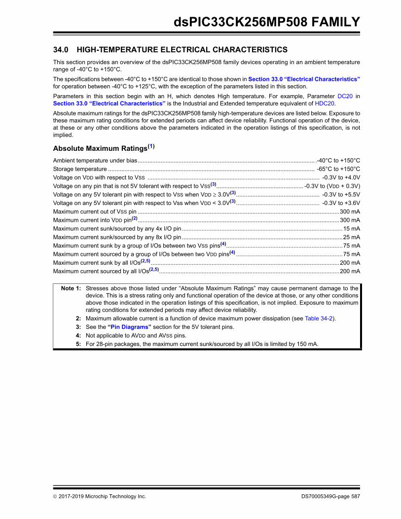
dsPIC33CK256MP508 FAMILY
34.0 HIGH-TEMPERATURE ELECTRICAL CHARACTERISTICSThis section provides an overview of the dsPIC33CK256MP508 family devices operating in an ambient temperaturerange of -40°C to +150°C. The specifications between -40°C to +150°C are identical to those shown in Section 33.0 “Electrical Characteristics”for operation between -40°C to +125°C, with the exception of the parameters listed in this section. Parameters in this section begin with an H, which denotes High temperature. For example, Parameter DC20 inSection 33.0 “Electrical Characteristics” is the Industrial and Extended temperature equivalent of HDC20.Absolute maximum ratings for the dsPIC33CK256MP508 family high-temperature devices are listed below. Exposure tothese maximum rating conditions for extended periods can affect device reliability. Functional operation of the device,at these or any other conditions above the parameters indicated in the operation listings of this specification, is notimplied.
Absolute Maximum Ratings(1)
Ambient temperature under bias............................................................................................................ .-40°C to +150°CStorage temperature .............................................................................................................................. -65°C to +150°CVoltage on VDD with respect to VSS ......................................................................................................... -0.3V to +4.0VVoltage on any pin that is not 5V tolerant with respect to VSS(3)..................................................... -0.3V to (VDD + 0.3V)Voltage on any 5V tolerant pin with respect to VSS when VDD 3.0V(3)................................................... -0.3V to +5.5VVoltage on any 5V tolerant pin with respect to Vss when VDD < 3.0V(3)................................................... -0.3V to +3.6VMaximum current out of VSS pin ...........................................................................................................................300 mAMaximum current into VDD pin(2)...........................................................................................................................300 mAMaximum current sunk/sourced by any 4x I/O pin..................................................................................................15 mAMaximum current sunk/sourced by any 8x I/O pin ..................................................................................................25 mAMaximum current sunk by a group of I/Os between two VSS pins(4).......................................................................75 mAMaximum current sourced by a group of I/Os between two VDD pins(4) .................................................................75 mAMaximum current sunk by all I/Os(2,5)...................................................................................................................200 mAMaximum current sourced by all I/Os(2,5)..............................................................................................................200 mA
Note 1: Stresses above those listed under “Absolute Maximum Ratings” may cause permanent damage to thedevice. This is a stress rating only and functional operation of the device at those, or any other conditionsabove those indicated in the operation listings of this specification, is not implied. Exposure to maximumrating conditions for extended periods may affect device reliability.
2: Maximum allowable current is a function of device maximum power dissipation (see Table 34-2).3: See the “Pin Diagrams” section for the 5V tolerant pins.4: Not applicable to AVDD and AVSS pins.5: For 28-pin packages, the maximum current sunk/sourced by all I/Os is limited by 150 mA.
2017-2019 Microchip Technology Inc. DS70005349G-page 587

dsPIC33CK256MP508 FAMILY
34.1 DC Characteristics
TABLE 34-1: OPERATING MIPS vs. VOLTAGEVDD Range Temperature Range Maximum CPU Clock Frequency
3.0V to 3.6V -40°C to +150°C 70
TABLE 34-2: THERMAL OPERATING CONDITIONSRating Symbol Min. Max. Unit
High-Temperature DevicesOperating Junction Temperature Range TJ -40 +165 °COperating Ambient Temperature Range TA -40 +150 °C
Power Dissipation:Internal Chip Power Dissipation:
PINT = VDD x (IDD – IOH) PD PINT + PI/O WI/O Pin Power Dissipation:
I/O = ({VDD – VOH} x IOH) + (VOL x IOL) Maximum Allowed Power Dissipation PDMAX (TJ – TA)/JA W
TABLE 34-3: THERMAL PACKAGING CHARACTERISTICS(1)
Characteristic Symbol Typ. Unit
Package Thermal Resistance, 80-Pin TQFP 12x12x1 mm JA 50.67 °C/WPackage Thermal Resistance, 64-Pin TQFP 10x10x1.0 mm JA 45.7 °C/WPackage Thermal Resistance, 64-Pin QFN 9x9 mm JA 18.7 °C/WPackage Thermal Resistance, 48-Pin TQFP 7x7 mm JA 62.76 °C/WPackage Thermal Resistance, 48-Pin UQFN 6x6 mm JA 27.6 °C/WPackage Thermal Resistance, 36-Pin UQFN 5x5 mm JA 29.2 °C/WPackage Thermal Resistance, 28-Pin UQFN 6x6 mm JA 22.41 °C/WPackage Thermal Resistance, 28-Pin SSOP 5.30 mm JA 52.84 °C/WNote 1: Junction to ambient thermal resistance, Theta-JA (JA) numbers are achieved by package simulations.
DS70005349G-page 588 2017-2019 Microchip Technology Inc.

dsPIC33CK256MP508 FAMILY
TABLE 34-4: OPERATING VOLTAGE SPECIFICATIONSOperating Conditions: 3.0V to 3.6V (unless otherwise stated)(1)
Operating temperature -40°C TA +150°C
Param No.
Symbol Characteristic Min. Typ. Max. Units Conditions
Operating VoltageDC10 VDD Supply Voltage 3.0 — 3.6 VDC11 AVDD Supply Voltage Greater of:
VDD – 0.3 or 3.0
— Lesser of:VDD + 0.3
or 3.6
V The difference between AVDD supply and VDD supply must not exceed ±300 mV at all times, including during device power-up
DC16 VPOR VDD Start Voltageto Ensure Internal Power-on Reset Signal
— — VSS V
DC17 SVDD VDD Rise Rateto Ensure InternalPower-on Reset Signal
0.03 — — V/ms 0V-3V in 100 ms
BO10 VBOR BOR Event on VDD Transition High-to-Low(2)
2.68 2.84 2.99 V
Note 1: Device is functional at VBORMIN < VDD < VDDMIN. Analog modules (ADC and comparators) may have degraded performance.
2: Parameters are characterized but not tested.
2017-2019 Microchip Technology Inc. DS70005349G-page 589

dsPIC33CK256MP508 FAMILY
TABLE 34-5: OPERATING CURRENT (IDD)(2)
Operating Conditions: 3.0V to 3.6V (unless otherwise stated)Operating temperature -40°C TA +150°C
Parameter No. Typ.(1) Max. Units Conditions
HDC20 13.6 33.5 mA +150°C 3.3V 10 MIPS (N1 = 1, N2 = 5, N3 = 2, M = 50, FVCO = 400 MHz,
FPLLO = 40 MHz)HDC21 16.2 36.0 mA +150°C 3.3V 20 MIPS (N1 = 1, N2 = 5, N3 = 1,
M = 50, FVCO = 400 MHz, FPLLO = 80 MHz)
HDC22 20.4 40.0 mA +150°C 3.3V 40 MIPS (N1 = 1, N2 = 3, N3 = 1, M = 60, FVCO = 480 MHz,
FPLLO = 160 MHz)HDC23 27.8 47.75 mA +150°C 3.3V 70 MIPS (N1 = 1, N2 = 2, N3 = 1,
M = 70, FVCO = 560 MHz, FPLLO = 280 MHz)
Note 1: Data in the “Typ.” column are for design guidance only and are not tested.2: Base Run current (IDD) is measured as follows:
• Oscillator is switched to EC+PLL mode in software• OSC1 pin is driven with external 8 MHz square wave with levels from 0.3V to VDD – 0.3V• OSC2 is configured as an I/O in the Configuration Words (OSCIOFNC (FOSC[2]) = 0)• FSCM is disabled (FCKSM[1:0] (FOSC[7:6]) = 01)• Watchdog Timer is disabled (FWDT[15] = 0 and WDTCONL[15] = 0)• All I/O pins (except OSC1) are configured as outputs and driving low• No peripheral modules are operating or being clocked (defined PMDx bits are all ‘1’s)• JTAG is disabled (JTAGEN (FICD[5]) = 0)• NOP instructions are executed in while(1) loop
DS70005349G-page 590 2017-2019 Microchip Technology Inc.

dsPIC33CK256MP508 FAMILY
TABLE 34-6: IDLE CURRENT (IIDLE)(2) Operating Conditions: 3.0V to 3.6V (unless otherwise stated)Operating temperature -40°C TA +150°C
Parameter No. Typ.(1) Max. Units Conditions
HDC40 11.6 33.25 mA +150°C 3.3V 10 MIPS (N1 = 1, N2 = 5, N3 = 2, M = 50, FVCO = 400 MHz,
FPLLO = 40 MHz)HDC41 12.7 33.75 mA +150°C 3.3V 20 MIPS (N1 = 1, N2 = 5, N3 = 1,
M = 50, FVCO = 400 MHz, FPLLO = 80 MHz)
HDC42 14.9 36.3 mA +150°C 3.3V 40 MIPS (N1 = 1, N2 = 3, N3 = 1, M = 60, FVCO = 480 MHz,
FPLLO = 160 MHz)HDC43 18.0 39.75 mA +150°C 3.3V 70 MIPS (N1 = 1, N2 = 2, N3 = 1,
M = 70, FVCO = 560 MHz, FPLLO = 280 MHz)
Note 1: Data in the “Typ.” column are for design guidance only and are not tested.2: Base Idle current (IIDLE) is measured as follows:
• Oscillator is switched to EC+PLL mode in software• OSC1 pin is driven with external 8 MHz square wave with levels from 0.3V to VDD – 0.3V• OSC2 is configured as an I/O in the Configuration Words (OSCIOFNC (FOSC[2]) = 0)• FSCM is disabled (FCKSM[1:0] (FOSC[7:6]) = 01)• Watchdog Timer is disabled (FWDT[15] = 0 and WDTCONL[15] = 0)• All I/O pins (except OSC1) are configured as outputs and driving low• No peripheral modules are operating or being clocked (defined PMDx bits are all ‘1’s)• JTAG is disabled (JTAGEN (FICD[5]) = 0)• Flash in standby with NVMSIDL (NVMCON[12]) = 1
2017-2019 Microchip Technology Inc. DS70005349G-page 591

dsPIC33CK256MP508 FAMILY
TABLE 34-7: POWER-DOWN CURRENT (IPD)(2)
Operating Conditions: 3.0V to 3.6V (unless otherwise stated)Operating temperature -40°C TA +150°C
Parameter No. Characteristic Typ.(1) Max. Units Conditions
HDC60 Base Power-Down Current 8.9 29.2 mA +150°C 3.3VNote 1: Data in the “Typ.” column are for design guidance only and are not tested.
2: Base Sleep current (IPD) is measured as follows:• OSC1 pin is driven with external 8 MHz square wave with levels from 0.3V to VDD – 0.3V• OSC2 is configured as an I/O in the Configuration Words (OSCIOFNC (FOSC[2]) = 0)• FSCM is disabled (FCKSM[1:0] (FOSC[7:6]) = 01)• Watchdog Timer is disabled (FWDT[15] = 0 and WDTCONL[15] = 0)• All I/O pins (except OSC1) are configured as outputs and driving low• No peripheral modules are operating or being clocked (defined PMDx bits are all ‘1’s)• JTAG is disabled (JTAGEN (FICD[5]) = 0)• The regulators are in Standby mode (VREGS (RCON[8]) = 0• The regulators are in Low-Power mode (LPWREN (VREGCON[15]) = 1
TABLE 34-8: DOZE CURRENT (IDOZE)Operating Conditions: 3.0V to 3.6V (unless otherwise stated)Operating temperature -40°C TA +150°C
Parameter No. Typ.(1) Max. Doze Ratio Units Conditions
HDC70 23.6 43 1:2 mA+150°C 3.3V
70 MIPS (N = 1, N2 = 2, N3 = 1,M = 70, FVCO = 560 MHz,
FPLLO = 280 MHz)18.5 38.7 1:128 mA
Note 1: Data in the “Typ.” column are for design guidance only and are not tested.
TABLE 34-9: WATCHDOG TIMER DELTA CURRENT (IWDT)(1) Operating Conditions: 3.0V to 3.6V (unless otherwise stated)Operating temperature -40°C TA +150°C
Parameter No. Typ. Max. Units Conditions
HDC61 24 120 µA +150°C 3.3VNote 1: The IWDT current is the additional current consumed when the module is enabled. This current should be
added to the base IPD current. All parameters are characterized but not tested during manufacturing.
DS70005349G-page 592 2017-2019 Microchip Technology Inc.

dsPIC33CK256MP508 FAMILY
TABLE 34-10: PWM DELTA CURRENT(1) Operating Conditions: 3.0V to 3.6V (unless otherwise stated)Operating temperature -40°C TA +150°C
Parameter No. Typ. Max. Units Conditions
HDC100 5.48 7.0 mA +150°C 3.3V PWM Output Frequency = 500 kHz,PWM Input (AFPLLO = 500 MHz)
(AVCO = 1000 MHz, PLLFBD = 125,APLLDIV1 = 2)
HDC101 4.44 5.7 mA +150°C 3.3V PWM Output Frequency = 500 kHz,PWM Input (AFPLLO = 400 MHz),(AVCO = 400 MHz, PLLFBD = 50,
APLLDIV1 = 1)HDC102 2.31 3.7 mA +150°C 3.3V PWM Output Frequency = 500 kHz,
PWM Input (AFPLLO = 200 MHz),(AVCO = 400 MHz, PLLFBD = 50,
APLLDIV1 = 2)HDC103 1.22 2.3 mA +150°C 3.3V PWM Output Frequency = 500 kHz,
PWM Input (AFPLLO = 100 MHz),(AVCO = 400 MHz, PLLFBD = 50,
APLLDIV1 = 4)Note 1: APLL current is not included. The APLL current will be the same if more than one PWM is running. Listed
delta currents are for only one PWM instance when HREN = 0 (PGxCONL[7]). All parameters are characterized but not tested during manufacturing.
TABLE 34-11: APLL DELTA CURRENTOperating Conditions: 3.0V to 3.6V (unless otherwise stated)Operating temperature -40°C TA +150°C
Parameter No. Typ. Max. Units Conditions(1)
HDC110 7.04 9.3 mA +150°C 3.3V AFPLLO = 500 MHz (AVCO = 1000 MHz, PLLFBD = 125,
APLLDIV1 = 2)HDC111 3.78 5.8 mA +150°C 3.3V AFPLLO = 400 MHz
(AVCO = 400 MHz, PLLFBD = 50, APLLDIV1 = 1)
HDC112 2.49 4.5 mA +150°C 3.3V AFPLLO = 200 MHz(AVCO = 400 MHz, PLLFBD = 50,
APLLDIV1 = 2)HDC113 1.83 3.6 mA +150°C 3.3V AFPLLO = 100 MHz
(AVCO = 400 MHz, PLLFBD = 50, APLLDIV1 = 4)
Note 1: The APLL current will be the same if more than one PWM or DAC is run to the APLL clock. All parameters are characterized but not tested during manufacturing.
2017-2019 Microchip Technology Inc. DS70005349G-page 593

dsPIC33CK256MP508 FAMILY
TABLE 34-12: ADC DELTA CURRENT(1) Operating Conditions: 3.0V to 3.6V (unless otherwise stated)Operating temperature -40°C TA +150°C
Parameter No. Typ. Max. Units Conditions
HDC120 3.76 6.8 mA +150°C 3.3V TAD = 14.3 ns(3.5 Msps conversion rate)
Note 1: Shared core continuous conversion. TAD = 14.3 nS (3.5 Msps conversion rate). Listed delta currents are for only one ADC core. All parameters are characterized but not tested during manufacturing.
TABLE 34-13: COMPARATOR + DAC DELTA CURRENTOperating Conditions: 3.0V to 3.6V (unless otherwise stated)Operating temperature -40°C TA +150°C
Parameter No. Typ. Max. Units Conditions
HDC130 1.25 1.65 mA +150°C 3.3V AFPLLO @ 500 MHz(1)
Note 1: APLL current is not included. Listed delta currents are for only one comparator + DAC instance. All parameters are characterized but not tested during manufacturing.
TABLE 34-14: OP AMP DELTA CURRENT(1)
Operating Conditions: 3.0V to 3.6V (unless otherwise stated)Operating temperature -40°C TA +150°C
Parameter No. Typ. Max. Units Conditions
HDC140 0.58 2.3 mA +150°C 3.3VNote 1: Listed delta currents are for only one op amp instance. All parameters are characterized but not tested
during manufacturing.
DS70005349G-page 594 2017-2019 Microchip Technology Inc.

dsPIC33CK256MP508 FAMILY
TABLE 34-15: I/O PIN INPUT SPECIFICATIONSOperating Conditions: 3.0V to 3.6V (unless otherwise stated)Operating temperature -40°C TA +150°C
Param No. Symbol Characteristic Min.(4) Typ.(1) Max.(5) Units Conditions
HDI50 IIL Input Leakage Current(2)
I/O Pins 5V Tolerant(3) -1500 — 1500 nAI/O Pins Not 5V Tolerant(3) -700 — 700 nAMCLR -1500 — 1500 nAOSCI -750 — 750 nA XT and HS modes
Note 1: Data in the “Typ.” column are at 3.3V, +25°C unless otherwise stated.2: Negative current is defined as current sourced by the pin.3: See the “Pin Diagrams” section for the 5V tolerant I/O pins.4: VPIN = VSS.5: VPIN = VDD.
TABLE 34-16: INTERNAL FRC ACCURACYOperating Conditions: 3.0V to 3.6V (unless otherwise stated)Operating temperature -40°C TA +150°C
Param No. Characteristic Min. Max. Units Conditions
Internal FRC Accuracy @ FRC Frequency = 8 MHz(1)
F20a FRC -3 +3 % -40°C TA +150°CNote 1: Frequency is calibrated at +25°C and 3.3V.
TABLE 34-17: INTERNAL LPRC ACCURACYOperating Conditions: 3.0V to 3.6V (unless otherwise stated)Operating temperature -40°C TA +150°C
ParamNo. Characteristic Min. Max. Units Conditions
LPRC @ 32 kHzF21 LPRC -27 +27 % -40°C TA +150°C
2017-2019 Microchip Technology Inc. DS70005349G-page 595

dsPIC33CK256MP508 FAMILY
TABLE 34-18: ADC MODULE SPECIFICATIONSOperating Conditions: 3.0V to 3.6V (unless otherwise stated)(1)
Operating temperature -40°C TA +150°C
Param No. Symbol Characteristics Min. Typical Max. Units Conditions
ADC AccuracyAD23c GERR Gain Error > -17.5 — < 17.5 LSb AVSS = 0V, AVDD = 3.3VAD24c EOFF Offset Error > -15 — < 15 LSb AVSS = 0V, AVDD = 3.3VNote 1: The ADC module is functional at VBORMIN < VDD < VDDMIN, but with degraded performance. Unless
otherwise stated, module functionality is ensured, but not characterized.
TABLE 34-19: DACx MODULE SPECIFICATIONSOperating Conditions: 3.0V to 3.6V (unless otherwise stated)Operating temperature -40°C TA +150°C
ParamNo. Symbol Characteristic Min. Typ.(1) Max. Units Comments
HDA03 INL Integral Nonlinearity Error -45 — 0 LSBNote 1: Parameters are for design guidance only and are not tested in manufacturing.
DS70005349G-page 596 2017-2019 Microchip Technology Inc.

dsPIC33CK256MP508 FAMILY
35.0 PACKAGING INFORMATION35.1 Package Marking Information
Legend: XX...X Customer-specific informationY Year code (last digit of calendar year)YY Year code (last 2 digits of calendar year)WW Week code (week of January 1 is week ‘01’)NNN Alphanumeric traceability code
Note: In the event the full Microchip part number cannot be marked on one line, it willbe carried over to the next line, thus limiting the number of availablecharacters for customer-specific information.
28-Lead UQFN (6x6 mm)
XXXXXXXXXXXXXXXXYYWWNNN
33CK64MP202
1710017
Example
XXXXXXX
36-Lead UQFN (5x5 mm)
XXXXXXXXXXXXXX
28-Lead SSOP (5.30 mm)
XXXXXXXXXXXXXXXXXXXXXXXX
YYWWNNN
Example
dsPIC33CK64MP202
1710017
YYWWNNN
dsPIC
Example
33CK64MP203
1710017
48-Lead TQFP (7x7 mm) Example
CK256MP5051710
017
2017-2019 Microchip Technology Inc. DS70005349G-page 597

dsPIC33CK256MP508 FAMILY
35.1 Package Marking Information (Continued)
48-Lead UQFN (6x6 mm)
64-Lead TQFP (10x10x1 mm)
XXXXXXXXXXXXXXXXXXXXXXXXXXXXXXXXX
YYWWNNN
Example
dsPIC33CK64MP206
1710017
80-Lead TQFP (12x12x1 mm)
XXXXXXXXXXXXXXXXXXXXXXXXXXXXXXXXXXXX
Example
dsPIC33CK64MP208
1710017
XXXXXXXXXXX
64-Lead QFN (9x9x0.9 mm)
XXXXXXXXXXXXXXXXXXXXXX
YYWWNNN
dsPIC33CK
Example
64MP2061710017
Example
YYWWNNN
PIC33CK256MP5051710017
DS70005349G-page 598 2017-2019 Microchip Technology Inc.

dsPIC33CK256MP508 FAMILY
35.2 Package Details
2017-2019 Microchip Technology Inc. DS70005349G-page 599

dsPIC33CK256MP508 FAMILY
Notes:
DS70005349G-page 600 2017-2019 Microchip Technology Inc.

dsPIC33CK256MP508 FAMILY
2017-2019 Microchip Technology Inc. DS70005349G-page 601

dsPIC33CK256MP508 FAMILY
BA
0.10 C
0.10 C
0.10 C A B0.05 C
(DATUM B)(DATUM A)
CSEATING
PLANE
NOTE 1
1
2
N
2X
TOP VIEW
SIDE VIEW
BOTTOM VIEW
NOTE 1
12
N
0.10 C A B
0.10 C A B
0.10 C
0.08 C
Microchip Technology Drawing C04-385 Rev C Sheet 1 of 2
2X
28X
For the most current package drawings, please see the Microchip Packaging Specification located athttp://www.microchip.com/packaging
Note:
28-Lead Ultra Thin Plastic Quad Flat, No Lead Package (2N) - 6x6x0.55 mm Body [UQFN]
D
E
E2
D2
2X P
28X b
e
A
(A3)
A1
28X K
With 4.65x4.65 mm Exposed Pad and Corner Anchors
8X b1
L
8X b2
DS70005349G-page 602 2017-2019 Microchip Technology Inc.

dsPIC33CK256MP508 FAMILY
Microchip Technology Drawing C04-385 Rev C Sheet 2 of 2
Number of Terminals
Overall Height
Terminal Width
Overall Width
Overall Length
Terminal Length
Exposed Pad Width
Exposed Pad Length
Terminal Thickness
Pitch
Standoff
UnitsDimension Limits
A1A
b
DE2
D2
A3
e
L
E
N0.65 BSC
0.127 REF
4.55
4.55
0.30
0.25
0.450.00
0.30
6.00 BSC
0.40
4.65
4.65
0.500.02
6.00 BSC
MILLIMETERSMIN NOM
28
4.75
4.75
0.50
0.35
0.550.05
MAX
K -0.20 -
REF: Reference Dimension, usually without tolerance, for information purposes only.BSC: Basic Dimension. Theoretically exact value shown without tolerances.
1.2.3.
Notes:
Pin 1 visual index feature may vary, but must be located within the hatched area.Package is saw singulatedDimensioning and tolerancing per ASME Y14.5M
Terminal-to-Exposed-Pad
For the most current package drawings, please see the Microchip Packaging Specification located athttp://www.microchip.com/packaging
Note:
Exposed Pad Corner Chamfer P - 0.35 -
28-Lead Ultra Thin Plastic Quad Flat, No Lead Package (2N) - 6x6x0.55 mm Body [UQFN]With 4.65x4.65 mm Exposed Pad and Corner Anchors
0.35 0.40 0.43Corner Anchor Pad b10.15 0.20 0.25Corner Pad, Metal Free Zone b2
2017-2019 Microchip Technology Inc. DS70005349G-page 603

dsPIC33CK256MP508 FAMILY
RECOMMENDED LAND PATTERN
Dimension LimitsUnits
C2
Optional Center Pad Width
Contact Pad Spacing
Optional Center Pad Length
Contact Pitch
Y2X2
4.754.75
MILLIMETERS
0.65 BSCMIN
EMAX
6.00
Contact Pad Length (X28)Contact Pad Width (X28)
Y1X1
0.800.35
Microchip Technology Drawing C04-2385B
NOM
SILK SCREEN
C1Contact Pad Spacing 6.00
Contact Pad to Pad (X28) G1 0.20
Thermal Via Diameter VThermal Via Pitch EV
0.331.20
BSC: Basic Dimension. Theoretically exact value shown without tolerances.
Notes:Dimensioning and tolerancing per ASME Y14.5M
For best soldering results, thermal vias, if used, should be filled or tented to avoid solder loss duringreflow process
1.
2.
For the most current package drawings, please see the Microchip Packaging Specification located athttp://www.microchip.com/packaging
Note:
C2
C1
EV
EV
E
X2
Y1
G2
G1
ØV
Contact Pad to Center Pad (X28) G2 0.20
28-Lead Ultra Thin Plastic Quad Flat, No Lead Package (2N) - 6x6x0.55 mm Body [UQFN]With 4.65x4.65 mm Exposed Pad and Corner Anchors
1
2
28
Y3
Corner Anchor Chamfer (X4)
Corner Anchor (X4)
X4
X3
0.35
1.00
Y4
X3
X4
Corner Anchor Chamfer (X4)
Corner Anchor (X4)
Y4
Y3
0.35
1.00
X1
Y2
DS70005349G-page 604 2017-2019 Microchip Technology Inc.

dsPIC33CK256MP508 FAMILY
B
A
0.10 C
0.10 C
0..07 C A B0.05 C
(DATUM B)(DATUM A)
C SEATINGPLANE
NOTE 1
12
N
2X
TOP VIEW
SIDE VIEW
BOTTOM VIEW
NOTE 1
12
N
0.10 C A B
0.10 C A B
0.10 C
0.08 C
Microchip Technology Drawing C04-436–M5 Rev B Sheet 1 of 2
D
E
A
16X b
e
2X
D2
E2
K
L
36X
For the most current package drawings, please see the Microchip Packaging Specification located athttp://www.microchip.com/packaging
Note:
36-Lead Ultra Thin Plastic Quad Flat, No Lead Package (M5) - 5x5 mm Body [UQFN]With Corner Anchors
SEEDETAIL A
2017-2019 Microchip Technology Inc. DS70005349G-page 605

dsPIC33CK256MP508 FAMILY
Microchip Technology Drawing C04-436–M5 Rev B Sheet 2 of 2
Number of Terminals
Overall Height
Terminal Width
Overall Width
Terminal Length
Exposed Pad Width
Terminal Thickness
Pitch
Standoff
UnitsDimension Limits
A1A
bE2
A3
e
L
E
N0.40 BSC
0.152 REF
3.60
0.300.15
0.500.00
0.200.40
3.70
0.550.02
5.00 BSC
MILLIMETERSMIN NOM
36
3.80
0.500.25
0.600.05
MAX
K 0.25 REF
REF: Reference Dimension, usually without tolerance, for information purposes only.BSC: Basic Dimension. Theoretically exact value shown without tolerances.
1.2.3.
Notes:
Pin 1 visual index feature may vary, but must be located within the hatched area.Package is saw singulatedDimensioning and tolerancing per ASME Y14.5M
Terminal-to-Exposed-Pad
36-Lead Ultra Thin Plastic Quad Flat, No Lead Package (M5) - 5x5 mm Body [UQFN]
For the most current package drawings, please see the Microchip Packaging Specification located athttp://www.microchip.com/packaging
Note:
With Corner Anchors
Overall LengthExposed Pad Length
DD2 3.60
5.00 BSC3.70 3.80
CSEATING
PLANE
(A3)
A1
A
DETAIL A
DS70005349G-page 606 2017-2019 Microchip Technology Inc.

dsPIC33CK256MP508 FAMILY
RECOMMENDED LAND PATTERN
Dimension LimitsUnits
C2
Center Pad Width
Contact Pad Spacing
Center Pad Length
Contact Pitch
Y2X2
3.803.80
MILLIMETERS
0.40 BSCMIN
EMAX
5.00
Contact Pad Length (X36Contact Pad Width (X36)
Y1X1
0.800.20
NOM
12
36
C1Contact Pad Spacing 5.00
Thermal Via Diameter VThermal Via Pitch EV
0.301.00
BSC: Basic Dimension. Theoretically exact value shown without tolerances.
Notes:Dimensioning and tolerancing per ASME Y14.5M
For best soldering results, thermal vias, if used, should be filled or tented to avoid solder loss duringreflow process
1.
2.
For the most current package drawings, please see the Microchip Packaging Specification located athttp://www.microchip.com/packaging
Note:
© 2019 Microchip Technology Inc.
Contact Pad to Center Pad (X36) G 0.20
Corner Pad Length (X4)Corner Pad Width (X4)
Y3X3
0.850.85
C1
C2
EV
EV
X2
Y2
Corner Pad Radius R 0.10
X3
Y3
X1
Y1
G
ØV
E SILK SCREEN
R
Microchip Technology Drawing C04-2436–M5 Rev B
36-Lead Ultra Thin Plastic Quad Flat, No Lead Package (M5) - 5x5 mm Body [UQFN]With Corner Anchors
2017-2019 Microchip Technology Inc. DS70005349G-page 607

dsPIC33CK256MP508 FAMILY
CSEATING
PLANE
TOP VIEW
SIDE VIEW
0.08 C
Microchip Technology Drawing C04-300-PT Rev D Sheet 1 of 2
48X
For the most current package drawings, please see the Microchip Packaging Specification located athttp://www.microchip.com/packaging
Note:
48-Lead Plastic Thin Quad Flatpack (PT) - 7x7x1.0 mm Body [TQFP]
D
D1D12
D2
E
E1
E12
E2
BA
e2
e
A A2
A1 48X b0.08 C A-B D
D
0.20 C A-B DN/4 TIPS
0.20 C A-B D 4X
AA
1 2 3
N
NOTE 1
DS70005349G-page 608 2017-2019 Microchip Technology Inc.

dsPIC33CK256MP508 FAMILY
For the most current package drawings, please see the Microchip Packaging Specification located athttp://www.microchip.com/packaging
Note:
REF: Reference Dimension, usually without tolerance, for information purposes only.BSC: Basic Dimension. Theoretically exact value shown without tolerances.
Notes:
1.2.
Pin 1 visual index feature may vary, but must be located within the hatched area.Dimensioning and tolerancing per ASME Y14.5M
Microchip Technology Drawing C04-300-PT Rev D Sheet 2 of 2
48-Lead Plastic Thin Quad Flatpack (PT) - 7x7x1.0 mm Body [TQFP]
H
SECTION A-A
2
1
c
(L1)L
2
R2
R1
Number of Terminals
Overall Height
Terminal Width
Overall Width
Terminal Length
Molded Package Width
Molded Package Thickness
Pitch
Standoff
UnitsDimension Limits
A1A
bE1
A2
e
L
E
N0.50 BSC
1.00
0.45
0.17
-0.05
0.22
0.60
--
MILLIMETERSMIN NOM
48
0.75
0.27
1.200.15
MAX
L1 1.00 REFFootprint
Overall LengthMolded Package Length
DD1
9.00 BSC7.00 BSC
Terminal Thickness c 0.09 - 0.16
R1R2
1
-0.08 -Lead Bend Radius-0.08 0.20Lead Bend Radius
3.5°0° 7°Foot Angle-0° -Lead Angle
2 12°11° 13°Mold Draft Angle
9.00 BSC7.00 BSC
0.95 1.05
2017-2019 Microchip Technology Inc. DS70005349G-page 609

dsPIC33CK256MP508 FAMILY
RECOMMENDED LAND PATTERN
Dimension LimitsUnits
C2Contact Pad Spacing
Contact Pitch
MILLIMETERS
0.50 BSCMIN
EMAX
8.40
Contact Pad Length (X48)Contact Pad Width (X48)
Y1X1
1.500.30
Microchip Technology Drawing C04-2300-PT Rev D
NOM
C1
C2
E
X1
Y1
G
C1Contact Pad Spacing 8.40
Distance Between Pads G 0.20
BSC: Basic Dimension. Theoretically exact value shown without tolerances.
Notes:Dimensioning and tolerancing per ASME Y14.5M
For best soldering results, thermal vias, if used, should be filled or tented to avoid solder loss duringreflow process
1.
2.
For the most current package drawings, please see the Microchip Packaging Specification located athttp://www.microchip.com/packaging
Note:
SILK SCREEN
1 2
48
48-Lead Plastic Thin Quad Flatpack (PT) - 7x7x1.0 mm Body [TQFP]
DS70005349G-page 610 2017-2019 Microchip Technology Inc.

dsPIC33CK256MP508 FAMILY
BA
0.10 C
0.10 C
0.07 C A B0.05 C
(DATUM B)(DATUM A)
C SEATINGPLANE
NOTE 1
12
N
2X
TOP VIEW
SIDE VIEW
BOTTOM VIEW
NOTE 1
12
N
0.10 C A B
0.10 C A B
0.10 C
0.08 C
Microchip Technology Drawing C04-442A-M4 Sheet 1 of 2
2X
52X
For the most current package drawings, please see the Microchip Packaging Specification located athttp://www.microchip.com/packaging
Note:
48-Lead Ultra Thin Plastic Quad Flat, No Lead Package (M4) - 6x6 mm Body [UQFN]With Corner Anchors and 4.6x4.6 mm Exposed Pad
D
E
D2
8X (b1)
E2
(K)
e2
e
48X bL
8X (b2)
A
(A3)
A1
2017-2019 Microchip Technology Inc. DS70005349G-page 611

dsPIC33CK256MP508 FAMILY
Microchip Technology Drawing C04-442A-M4 Sheet 2 of 2
REF: Reference Dimension, usually without tolerance, for information purposes only.BSC: Basic Dimension. Theoretically exact value shown without tolerances.
1.2.3.
Notes:
Pin 1 visual index feature may vary, but must be located within the hatched area.Package is saw singulatedDimensioning and tolerancing per ASME Y14.5M
48-Lead Ultra Thin Plastic Quad Flat, No Lead Package (M4) - 6x6 mm Body [UQFN]
For the most current package drawings, please see the Microchip Packaging Specification located athttp://www.microchip.com/packaging
Note:
With Corner Anchors and 4.6x4.6 mm Exposed Pad
Number of Terminals
Overall Height
Terminal Width
Overall Width
Terminal Length
Exposed Pad Width
Terminal Thickness
Pitch
Standoff
UnitsDimension Limits
A1A
bE2
A3
e
L
E
N0.40 BSC
0.15 REF
0.35
0.15
0.500.00
0.20
0.40
0.550.02
6.00 BSC
MILLIMETERSMIN NOM
48
0.45
0.25
0.600.05
MAX
K 0.30 REFTerminal-to-Exposed-Pad
Overall LengthExposed Pad Length
DD2 4.50
6.00 BSC4.60 4.70
Corner Anchor Pad b1 0.45 REFCorner Anchor Pad, Metal-free Zone b2 0.23 REF
4.50 4.60 4.70
DS70005349G-page 612 2017-2019 Microchip Technology Inc.

dsPIC33CK256MP508 FAMILY
RECOMMENDED LAND PATTERN
Dimension LimitsUnits
C2
Center Pad Width
Contact Pad Spacing
Center Pad Length
Contact Pitch
Y2X2
4.704.70
MILLIMETERS
0.40 BSCMIN
EMAX
6.00
Contact Pad Length (X48)Contact Pad Width (X48)
Y1X1
0.800.20
Microchip Technology Drawing C04-2442A-M4
NOM
48-Lead Ultra Thin Plastic Quad Flat, No Lead Package (M4) - 6x6 mm Body [UQFN]
12
48
C1Contact Pad Spacing 6.00
Contact Pad to Center Pad (X48) G1 0.25
Thermal Via Diameter VThermal Via Pitch EV
0.331.20
BSC: Basic Dimension. Theoretically exact value shown without tolerances.
Notes:Dimensioning and tolerancing per ASME Y14.5M
For best soldering results, thermal vias, if used, should be filled or tented to avoid solder loss duringreflow process
1.
2.
For the most current package drawings, please see the Microchip Packaging Specification located athttp://www.microchip.com/packaging
Note:
With Corner Anchors and 4.6x4.6 mm Exposed Pad
Pad Corner Radius (X 20) R 0.10
C1
C2
EV
EV
X2
Y2
X3
Y3
Y1
E
X1
G2
G1
R
Contact Pad to Contact Pad G2 0.20
Corner Anchor Pad Length (X4)Corner Anchor Pad Width (X4)
Y3X3
0.900.90
ØV
SILK SCREEN
2017-2019 Microchip Technology Inc. DS70005349G-page 613

dsPIC33CK256MP508 FAMILY
0.20 C A-B D
64 X b0.08 C A-B D
CSEATING
PLANE
4X N/4 TIPS
TOP VIEW
SIDE VIEW
For the most current package drawings, please see the Microchip Packaging Specification located athttp://www.microchip.com/packaging
Note:
Microchip Technology Drawing C04-085C Sheet 1 of 2
64-Lead Plastic Thin Quad Flatpack (PT)-10x10x1 mm Body, 2.00 mm Footprint [TQFP]
D
EE1
D1
D
A B
0.20 H A-B D4X
D1/2
e
A
0.08 C
A1
A2
SEE DETAIL 1AA
E1/2
NOTE 1
NOTE 2
1 2 3
N
0.05
DS70005349G-page 614 2017-2019 Microchip Technology Inc.

dsPIC33CK256MP508 FAMILY
For the most current package drawings, please see the Microchip Packaging Specification located athttp://www.microchip.com/packaging
Note:
64-Lead Plastic Thin Quad Flatpack (PT)-10x10x1 mm Body, 2.00 mm Footprint [TQFP]
13°12°11°Mold Draft Angle Bottom13°12°11°Mold Draft Angle Top0.270.220.17bLead Width0.20-0.09cLead Thickness
10.00 BSCD1Molded Package Length10.00 BSCE1Molded Package Width12.00 BSCDOverall Length12.00 BSCEOverall Width
7°3.5°0°Foot Angle
0.750.600.45LFoot Length0.15-0.05A1Standoff1.051.000.95A2Molded Package Thickness1.20--AOverall Height
0.50 BSCeLead Pitch64NNumber of Leads
MAXNOMMINDimension LimitsMILLIMETERSUnits
Footprint L1 1.00 REF
2. Chamfers at corners are optional; size may vary.1. Pin 1 visual index feature may vary, but must be located within the hatched area.
4. Dimensioning and tolerancing per ASME Y14.5MBSC: Basic Dimension. Theoretically exact value shown without tolerances.REF: Reference Dimension, usually without tolerance, for information purposes only.
3. Dimensions D1 and E1 do not include mold flash or protrusions. Mold flash orprotrusions shall not exceed 0.25mm per side.
Notes:
Microchip Technology Drawing C04-085C Sheet 2 of 2
L(L1)
c
H
X
X=A—B OR D
e/2
DETAIL 1
SECTION A-A
2017-2019 Microchip Technology Inc. DS70005349G-page 615

dsPIC33CK256MP508 FAMILY
RECOMMENDED LAND PATTERN
For the most current package drawings, please see the Microchip Packaging Specification located athttp://www.microchip.com/packaging
Note:
Dimension LimitsUnits
C1Contact Pad SpacingContact Pad Spacing
Contact Pitch
C2
MILLIMETERS
0.50 BSCMIN
EMAX
11.4011.40
Contact Pad Length (X28)Contact Pad Width (X28)
Y1X1
1.500.30
BSC: Basic Dimension. Theoretically exact value shown without tolerances.
Notes:1. Dimensioning and tolerancing per ASME Y14.5M
Microchip Technology Drawing C04-2085B Sheet 1 of 1
GDistance Between Pads 0.20
NOM
64-Lead Plastic Thin Quad Flatpack (PT)-10x10x1 mm Body, 2.00 mm Footprint [TQFP]
C2
C1
E
G
Y1
X1
DS70005349G-page 616 2017-2019 Microchip Technology Inc.

dsPIC33CK256MP508 FAMILY
Note: For the most current package drawings, please see the Microchip Packaging Specification located at http://www.microchip.com/packaging
2017-2019 Microchip Technology Inc. DS70005349G-page 617

dsPIC33CK256MP508 FAMILY
Note: For the most current package drawings, please see the Microchip Packaging Specification located at http://www.microchip.com/packaging
DS70005349G-page 618 2017-2019 Microchip Technology Inc.

dsPIC33CK256MP508 FAMILY
For the most current package drawings, please see the Microchip Packaging Specification located athttp://www.microchip.com/packaging
Note:
2017-2019 Microchip Technology Inc. DS70005349G-page 619

dsPIC33CK256MP508 FAMILY
���������� ������������� ������������������ �!"�#����$���%
& ��'�� �����!�"#�����$ %�& �'#� �(���!���)�*#'�(#"'�* �����' $�+�'����'� ���'�� $��� ���� ,��(& �"��'����� �"��� ��'�����-�"�. �(���!������ ��( �"���"������$�/��$����'�����#$ �(��$�&��"�������'�#"���"�����$�&��"�������'�#"���"�"�������'� %� $����0�((� ��"�$ ��� ��( �"���������$�'�� �������� �����/�1���0��
2�,3 2�"�����( �"������� �� '������� %��'�!��# �"��+��+�'��#'�'�� ���� "��/43 � & � �� ���( �"���)�#"#�����+�'��#'�'�� ���� )�&�����&��(�'����#��" "������
& �' 4���'� �(�"'��#�� �'���5�� �$��+���")�� �" �" �'� ���������� ��5������� ��&���'��������' $��'��''366+++�(����������(6��5�����
7��'" ��88��/�/����( �"����8�(�'" ��9 9:� ��;
9#(* ���&�8 �$" 9 ��8 �$� �'�� ��0��2�,:! �����< ���' � = = �������$ $� ��5�� �����5� "" �� ���0 ���� ���0�'��$�&&�� �� ���0 = ���04��'�8 ��'� 8 ���0 ��>� ���04��'���' 8� ������/44��'����� � �? ��0? �?:! �����@�$'� / ������2�,:! �����8 ��'� � ������2�,���$ $� ��5�� �@�$'� /� ������2�,���$ $� ��5�� �8 ��'� �� ������2�,8 �$�����5� "" � ���� = ����8 �$�@�$'� * ���� ���� �������$����&'����� ��� � ��? ��? ��?���$����&'����� �2�''�( � ��? ��? ��?
D
D1
E
E1e
b N
NOTE 112 3 NOTE 2
A
A2L1
A1L
c
α
βφ
�������� � �������� ���+��� ,�����2
DS70005349G-page 620 2017-2019 Microchip Technology Inc.

dsPIC33CK256MP508 FAMILY
Note: For the most current package drawings, please see the Microchip Packaging Specification located at http://www.microchip.com/packaging
2017-2019 Microchip Technology Inc. DS70005349G-page 621

dsPIC33CK256MP508 FAMILY
NOTES:
DS70005349G-page 622 2017-2019 Microchip Technology Inc.

dsPIC33CK256MP508 FAMILY
APPENDIX A: REVISION HISTORY
Revision A (December 2017)This is the initial version of the document.
Revision B (May 2018)This revision incorporates the following updates:• Sections:
- Updated Section 4.2.7 “BIST at Start-up”, Section 4.2.8 “BIST at Run Time”, Section 15.0 “Quadrature Encoder Interface (QEI)”, Section 30.2 “Device Calibration and Identification”, Section 30.10 “Code Protection and CodeGuard™ Security” and Section 35.1 “Package Marking Information”.
- Added Section 5.3.2 “Error Correcting Code (ECC)” and Section 5.5.4 “ECC Control Registers”.
• Tables:- Updated Table 4-3, Table 4-9, Table 7-3,
Table 7-4, Table 7-5, Table 8-7, Table 15-1, Table 24-3, Table 30-3, Table 33-1, Table 33-3, Table 33-5, Table 33-6 (was Table 33-9), Table 33-7 (was Table 33-11), Table 33-22, Table 33-37 and Table 33-40.
- Deleted Table 33-6, Table 33-7, Table 33-8 and Table 33-10.
- Added Table 33-10, Table 33-11, Table 33-12 and Table 33-13.
• Figures:- Updated Figure 3-1, Figure 4-1, Figure 4-12,
Figure 15-2, Figure 30-3 and Figure 30-4.• Registers:
- Updated Register 4-1, Register 14-1, Register 14-6, Register 14-7, Register 14-9, Register 15-1, Register 15-2, Register 15-3, Register 15-5, Register 15-6, Register 15-7, Register 15-9, Register 15-11, Register 15-17, Register 27-1, Register 27-2, Register 30-5 and Register 30-7.
- Added Register 5-7, Register 5-8, Register 5-9, Register 5-10, Register 5-11, Register 5-12, Register 15-18 and Register 15-19.
- Deleted Register 15-8, Register 15-12 and Register 15-20.
• Examples:- Updated Example 29-1.- Added Example 29-2.
• Equations:- Deleted Equation 4-1.
Revision C (July 2018)This revision incorporates the following updates:• Tables:
- Updated Table 1-1, Table 33-10, Table 33-20, Table 33-21, Table 33-26 and Table 33-41.
• Registers:- Updated Register 4-1, Register 10-1,
Register 12-12, Register 12-13, Register 13-30, Register 14-6, Register 14-7, Register 15-2, Register 16-4, Register 20-2, Register 22-7, Register 28-5, Register 28-6, Register 28-7, Register 28-8, Register 28-9, Register 28-10 and Register 28-11.
• Figures:- Updated Figure 13-1 and Figure 13-2.
Revision D (September 2018)This revision incorporates the following updates:• Sections:
- Updated Section 18.0 “Inter-Integrated Circuit (I2C)”.
- Added Section 18.4 “SMBus Support”.- Updated the packaging diagrams for the
28-Lead SSOP and 28-Lead UQFN in Section 35.0 “Packaging Information”.
• Tables:- Updated Table 33-5, Table 33-6, Table 33-7,
Table 33-8, Table 33-13 and Table 33-23.- Added Table 18-3.
• Registers:- Updated Register 12-9, Register 13-3,
Register 30-6 and Register 30-21.• Figures:
- Updated Figure 9-4.
2017-2019 Microchip Technology Inc. DS70005349G-page 623

dsPIC33CK256MP508 FAMILY
Revision E (December 2018)This revision incorporates the following updates:• Sections:
- Updated the “Operating Conditions”, “Safety Features” and “Pin Diagrams” sections.
- Updated Section 5.0 “Flash Program Memory”, Section 5.2 “RTSP Operation”, Section 5.3.1 “Programming Algorithm for Flash Program Memory”, Section 5.3.3 “ECC Fault Injection”, Section 8.5.5 “Input Mapping”, Section 12.0 “High-Resolution PWM with Fine Edge Placement”, Section 23.1 “Control Registers” and the “Product Identification System” section.
- Added Section 8.5.3 “Controlling Configuration Changes”, Section 8.5.3.1 “Control Register Lock”, Section 8.5.4 “Considerations for Peripheral Pin Selection”, Section 9.10 “OSCCON Unlock Sequence”, Section 12.3 “Lock and Write Restrictions”and Section 34.0 “High-Temperature Electrical Characteristics”.
• Tables:- Added Table 7-1 and Table 12-1.- Updated Table 7-2, Table 26-1, Table 33-4,
Table 33-39 and Table 33-41.• Registers:
- Added Register 3-3 and Register 5-6.- Updated Register 5-5, Register 8-13,
Register 9-1, Register 9-4, Register 12-1, Register 13-6, Register 16-1, Register 17-1 and Register 30-14.
• Figures:- Updated Figure 17-1 and Figure 17-2.
• Examples:- Added Example 5-1 and Example 8-1.
Revision F (March 2019)This revision incorporates the following updates:• Sections:
- Updated the “Operating Conditions”, “Qualification and Class B Support”, “Absolute Maximum Ratings(1)” and “Product Identification System”sections.
- Updated Section 9.0 “Oscillator with High-Frequency PLL”.
- Added Section 9.7 “Backup Internal Fast RC (BFRC) Oscillator”, Section 9.8 “Reference Clock Output”, Section 12.4 “PWM4H/L Output on Peripheral Pin Select”, Section 13.2 “Temperature Sensor” and Section 34.0 “High-Temperature Electrical Characteristics”.
• Tables:- Updated Table 3, Table 4, Table 5, Table 6,
Table 7, Table 8, Table 1-1, Table 4-10, Table 4-11, Table 4-16, Table 8-7, Table 10-1, Table 12-1, Table 33-4, Table 33-7, Table 33-8 and Table 33-40.
• Registers:- Updated Register 12-14, Register 12-16,
Register 12-32, Register 15-2 and Register 22-2.
• Equations:- Updated Equation 18-1.
• Figures:- Updated Figure 22-1.
Updated bit brackets from ‘<x>’ to ‘[x]’ and minor textedits throughout document.
DS70005349G-page 624 2017-2019 Microchip Technology Inc.

dsPIC33CK256MP508 FAMILY
Revision G (October 2019)This revision incorporates the following updates:• Sections:
- Updated CodeGuard™ Intermediate Security FRM reference in “Referenced Sources”
- Updated Section 1.0 “Device Overview”, Section 2.4 “ICSP Pins”, Section 4.1.3 “Unique Device Identifier (UDID)”, Section 4.4.3.2 “W Address Register Selection”, Section 5.3.2 “Error Correcting Code (ECC)”, Section 10.4 “Registers”, Section 14.1 “Overview”, Section 20.0 “Single-Edge Nibble Transmission (SENT)”, Section 27.0 “Operational Amplifier”, Section 32.0 “Development Support” and updated the 36-Lead (M5) package diagrams to Rev B.
• Tables:- Updated Table 1, Table 2, Table 7-2,
Table 8-4, Table 8-6, Table 8-14, Table 10-1, Table 24-3, Table 30-2 and Table 33-36.
• Registers:- Updated Register 3-2, Register 7-2,
Register 7-3, Register 7-5, Register 7-7, Register 8-9, Register 8-10, Register 8-11, Register 8-12, Register 11-8, Register 11-28, Register 11-44, Register 12-13, Register 12-14, Register 12-17, Register 13-5, Register 13-19, Register 13-31, Register 14-9, Register 20-1, Register 23-3, Register 24-1, Register 25-3, Register 25-4, Register 30-6 and Register 30-21.
• Figures:- Updated Figure 4-4, Figure 13-1 and
Figure 26-1.
2017-2019 Microchip Technology Inc. DS70005349G-page 625

dsPIC33CK256MP508 FAMILY
NOTES:
DS70005349G-page 626 2017-2019 Microchip Technology Inc.

dsPIC33CK256MP508 FAMILY
INDEXAAbsolute Maximum Ratings ...................................... 551, 587AC Characteristics ............................................................ 563
Load Conditions ........................................................ 563Alternate Interrupt Vector Table........................................ 101Analog-to-Digital Converter. See ADC.Arithmetic Logic Unit (ALU)................................................. 39Auto-Shutdown and Gating Sources................................. 447
BBit-Reversed Addressing .................................................... 74
Example ...................................................................... 75Implementation ........................................................... 74Sequence Table (16-Entry)......................................... 75
Block Diagrams16-Bit Timer1 Module................................................ 435ADC Module.............................................................. 300ADC Shared Core ..................................................... 301Addressing for Table Registers................................... 79APLL and VCO Detail ............................................... 187CALL Stack Frame...................................................... 70CAN FD Module........................................................ 220CLCx Input Source Selection.................................... 455CLCx Logic Function Combinatorial Options ............ 454CLCx Module ............................................................ 453Conceptual SCCPx Modules .................................... 439Constant-Current Source .......................................... 485CPU Core.................................................................... 30CRC Module ............................................................. 481Data Access from Program Space
Address Generation............................................ 76Deadman Timer Module ........................................... 493Dedicated ADC Core ................................................ 301dsPIC33CK256MP508 Core Clock Sources............. 183dsPIC33CK256MP508 Core
Oscillator Subsystem ........................................ 184dsPIC33CK256MP508 Family .................................... 17Functional Direct Memory Access (DMA) ................. 210High-Speed Analog Comparator............................... 330I2Cx Module.............................................................. 402Interleaved PFC .......................................................... 26Internal Regulator ..................................................... 532Master Reset System.................................................. 95MCLR Pin Connections............................................... 24Multiplexing Remappable Outputs for RPn............... 136Off-Line UPS............................................................... 28Operational Amplifier ................................................ 489Phase-Shifted Full-Bridge Converter .......................... 27PLL and VCO............................................................ 185PMP Pinout and Connections to
External Devices ............................................... 411Programmer’s Model................................................... 32PSV Read Address Generation .................................. 67PTG........................................................................... 466PWM High-Level Module .......................................... 264QEI Module ............................................................... 343Recommended Minimum Connection......................... 24Reference Clock Generator ...................................... 191Remappable Input for U1RX..................................... 131Security Segments.................................................... 538Security Segments (Dual Partition)........................... 538SENTx Module.......................................................... 426Shared Port Structure ............................................... 121
Simplified UARTx ..................................................... 362SPIx Master, Frame Master Connection .................. 399SPIx Master, Frame Slave Connection .................... 400SPIx Master/Slave Connection
(Enhanced Buffer Modes)................................. 399SPIx Master/Slave Connection (Standard Mode)..... 398SPIx Module (Enhanced Mode)................................ 386SPIx Module (Standard Mode) ................................. 385SPIx Slave, Frame Master Connection .................... 400SPIx Slave, Frame Slave Connection ...................... 400Suggested Oscillator Circuit Placement ..................... 25Timer Clock Generator ............................................. 440Watchdog Timer (WDT)............................................ 534
Brown-out Reset (BOR)............................................ 513, 533Built-In Self-Test (BIST)...................................................... 50
At Run Time................................................................ 50At Start-up .................................................................. 50Flowchart .................................................................... 50
Built-In Self-Test. See BIST.
CCAN FD Module
Control Registers...................................................... 221Features ................................................................... 219Message Reception.................................................. 219
Capture/Compare/PWM/TimerAuto-Shutdown and Gating Sources ........................ 447Auxiliary Output ........................................................ 442Control Registers...................................................... 443General Purpose Timer ............................................ 440Input Capture Mode.................................................. 441Output Compare Mode ............................................. 441Synchronization Sources.......................................... 446Time Base Generator ............................................... 440
Capture/Compare/PWM/Timer (SCCP/MCCP) ................ 439CLC
Control Registers...................................................... 456Code Examples
Configuring UART1 Input and Output Functions ...... 131Flash Write/Read........................................................ 81PWRSAV Instruction Syntax in Assembly................... 501PWRSAV Instruction Syntax in C Language............... 501Using Auxiliary PLL with Internal FRC Oscillator...... 188Using PLL (50 MIPS) with POSC ............................. 190Using Primary PLL with 8 MHz Internal FRC ........... 186
Code Protection........................................................ 513, 537CodeGuard Security ................................................. 513, 537Comparator/DAC
Control Registers...................................................... 331Features Overview ................................................... 331
Configurable Logic Cell (CLC) .......................................... 453Configurable Logic Cell. See CLC.Configuration Bits ............................................................. 513
Bit Values for Clock Selection .................................. 193Controller Area Network. See CAN.CPU .................................................................................... 29
Addressing Modes...................................................... 29Control Registers........................................................ 34Data Space Addressing.............................................. 29Instruction Set............................................................. 29Registers .................................................................... 29Resources .................................................................. 33
CRCControl Registers...................................................... 482
2017-2019 Microchip Technology Inc. DS70005349G-page 627

dsPIC33CK256MP508 FAMILY
Current Bias GeneratorControl Registers ...................................................... 486
Current Bias Generator (CBG).......................................... 485Current Bias Generator. See CBG.Customer Change Notification Service ............................. 635Customer Notification Service........................................... 635Customer Support ............................................................. 635Cyclic Redundancy Check. See CRC.
DData Address Space ........................................................... 45
Memory Map for dsPIC33CK128MPX0X Devices ...... 48Memory Map for dsPIC33CK256MP508 Devices ....... 47Memory Map for dsPIC33CK64MPX0X and
dsPIC33CK32MPX0X Devices ........................... 49Near Data Space ........................................................ 46Organization, Alignment.............................................. 45SFR Space.................................................................. 46Width........................................................................... 45
Data SpaceExtended X ................................................................. 70Paged Data Memory Space (figure) ........................... 68Paged Memory Scheme ............................................. 67
DC CharacteristicsOperating MIPS vs. Voltage...................................... 552
Deadman Timer (DMT) ..................................................... 493Control Registers ...................................................... 494
Deadman Timer. See DMT.Development Support ....................................................... 549Device Calibration ............................................................. 530
and Identification....................................................... 530Device Overview ................................................................. 17Direct Memory Access Controller. See DMA.DMA
Channel Trigger Sources .......................................... 217Control Registers ...................................................... 213Peripheral Module Disable (PMD) ............................ 213Summary of Operations ............................................ 211Types of Data Transfers ........................................... 212Typical Setup ............................................................ 213
Doze Mode........................................................................ 503DSP Engine......................................................................... 39Dual Watchdog Timer (Dual WDT) ................................... 534
EECC
Control Registers ........................................................ 92Electrical Characteristics................................................... 551
AC ............................................................................. 563ADC Delta Current .................................................... 558ADC Specifications ................................................... 583APLL Delta Current ................................................... 558APLL Timing Specifications ...................................... 565Comparator + DAC Delta Current ............................. 559Constant-Current Source Specifications................... 586DACx Output (DACOUT1 Pin) Specifications........... 585DACx Specifications ................................................. 585Doze Current (IDOZE) ................................................ 556External Clock Requirements ................................... 564High-Speed Analog Comparator Specifications........ 584High-Speed PWMx Timing Requirements ................ 569I/O Pin Input Injection Current Specifications ........... 561I/O Pin Input Specifications ....................................... 560I/O Pin Output Specifications .................................... 561I/O Timing Requirements .......................................... 567
I2Cx Bus Data Timing Requirements (Master Mode) .................................................. 579
I2Cx Bus Data Timing Requirements (Slave Mode) .................................................... 581
Idle Current (IIDLE) .................................................... 555Internal FRC Accuracy.............................................. 566Internal LPRC Accuracy ........................................... 566Op Amp Delta Current .............................................. 559Operating Current (IDD) ............................................ 554Operating Voltage Specifications.............................. 553Operational Amplifier Specifications ......................... 586PLL Timing Specifications ........................................ 565Power-Down Current (IPD)........................................ 556Program Memory ...................................................... 562PWM Delta Current................................................... 557Reset, WDT, OST, PWRT Timing Requirements ..... 568SPIx Master Mode (Full-Duplex, CKE = 0,
CKP = x, SMP = 1) Timing Requirements ........ 573SPIx Master Mode (Full-Duplex, CKE = 1,
CKP = x, SMP = 1) Timing Requirements ........ 572SPIx Master Mode (Half-Duplex, Transmit Only)
Timing Requirements ....................................... 571SPIx Maximum Data/Clock Rate Summary .............. 570SPIx Slave Mode (Full-Duplex, CKE = 0,
CKP = x, SMP = 0) Timing Requirements ........ 575SPIx Slave Mode (Full-Duplex, CKE = 1,
CKP = x, SMP = 0) Timing Requirements ........ 577UARTx I/O Timing Requirements ............................. 582Watchdog Timer Delta Current (IWDT).................... 557
EquationsAFPLLO Calculation ................................................... 188AFVCO Calculation .................................................... 188Calculating Frequency Output .................................. 192FPLLO Calculation ..................................................... 186Frame Time Calculations.......................................... 427FVCO Calculation ...................................................... 186I2C Baud Rate Reload Calculation ........................... 403Relationship Between Device and
SPIx Clock Speed............................................. 400SYNCMINx and SYNCMAXx Calculations ............... 428Tick Period Calculation ............................................. 427
Errata .................................................................................. 15Error Correcting Code (ECC).............................................. 82
Fault Injection ............................................................. 82
FFlash Program Memory
and Table Instructions ................................................ 79Control Registers ........................................................ 86Dual Partition Flash Configuration .............................. 84Operations .................................................................. 81RTSP Operation ......................................................... 80
Flexible Configuration ....................................................... 513
GGetting Started Guidelines.................................................. 23
Connection Requirements .......................................... 23Decoupling Capacitors................................................ 23External Oscillator Pins............................................... 25ICSP Pins ................................................................... 25Master Clear (MCLR) Pin ........................................... 24Oscillator Value Conditions on Start-up...................... 26Targeted Applications ................................................. 26Unused I/Os................................................................ 26
DS70005349G-page 628 2017-2019 Microchip Technology Inc.

dsPIC33CK256MP508 FAMILY
HHigh-Resolution PWM (HSPWM) with
Fine Edge Placement................................................ 263High-Speed Analog Comparator with
Slope Compensation DAC ........................................ 329High-Speed, 12-Bit Analog-to-Digital Converter (ADC) .... 299
Control Registers ...................................................... 303Features Overview.................................................... 299Resources................................................................. 302Temperature Sensor ................................................. 302
High-Temperature DC CharacteristicsADC Delta Current .................................................... 594ADC Specifications ................................................... 596APLL Delta Current................................................... 593Comparator + DAC Delta Current ............................. 594DACx Specifications ................................................. 596Doze Current (IDOZE) ................................................ 592I/O Pin Input Specifications....................................... 595Idle Current (IIDLE) .................................................... 591Internal FRC Accuracy.............................................. 595Internal LPRC Accuracy............................................ 595Op Amp Delta Current .............................................. 594Operating Current (IDD)............................................. 590Operating MIPS vs. Voltage...................................... 588Operating Voltage Specifications.............................. 589Power-Down Current (IPD) ........................................ 592PWM Delta Current................................................... 593Thermal Operating Conditions .................................. 588Thermal Packaging Characteristics .......................... 588Watchdog Timer Delta Current (IWDT) .................... 592
High-Temperature Electrical Characteristics..................... 587HSPWM
Architecture............................................................... 264Control Registers ...................................................... 266Lock and Write Restrictions ...................................... 265PWM Output Availability (table) ................................ 263
II/O Ports
Configuring Analog/Digital Port Pins......................... 122Control Registers ...................................................... 122Helpful Tips ............................................................... 141Parallel I/O (PIO)....................................................... 119Resources................................................................. 142Write/Read Timing .................................................... 122
I2CClock Rates............................................................... 403Communicating as Master in Single
Master Environment.......................................... 401Control Registers ...................................................... 405Reserved Addresses................................................. 404Setting Baud Rate as Bus Master............................. 403Slave Address Masking ............................................ 403SMBus Support......................................................... 404
ICSP Write Inhibit................................................................ 83Activation .................................................................... 83
In-Circuit Debugger ........................................................... 537In-Circuit Emulation........................................................... 513In-Circuit Serial Programming (ICSP) ....................... 513, 537Input Change Notification (ICN) ........................................ 129
Instruction Addressing Modes ............................................ 71File Register Instructions ............................................ 71Fundamental Modes Supported ................................. 71MAC Instructions.......................................................... 72MCU Instructions ........................................................ 71Move and Accumulator Instructions ........................... 72Other Instructions ....................................................... 72
Instruction Set Summary .................................................. 539Overview................................................................... 542Symbols Used in Opcode Descriptions .................... 540
Instruction-Based Power-Saving Modes........................... 501Idle............................................................................ 502Sleep ........................................................................ 502
Inter-Integrated Circuit. See I2C.Internet Address ............................................................... 635Interrupt Controller
Alternate Interrupt Vector Table (AIVT) ...................... 99Control and Status Registers.................................... 110
INTCON1.......................................................... 110INTCON2.......................................................... 110INTCON3.......................................................... 110INTCON4.......................................................... 110INTTREG.......................................................... 110
Interrupt Vector Details............................................. 103Interrupt Vector Table (IVT)........................................ 99Reset Sequence ......................................................... 99Resources ................................................................ 110Trap Vector Details................................................... 102
Interrupt Vector Table ....................................................... 100Interrupts Coincident with Power Save Instructions ......... 502
JJTAG Boundary Scan Interface ........................................ 513JTAG Interface ................................................................. 537
LLow-Power Sleep Modes (table)....................................... 502
MMemory Organization ......................................................... 41
Resources .................................................................. 52Microchip Internet Website ............................................... 635Modulo Addressing ............................................................. 73
Applicability................................................................. 74Operation Example..................................................... 73Start and End Address ............................................... 73W Address Register Selection.................................... 73
OOperational Amplifier ........................................................ 489
Control Registers...................................................... 490Oscillator
Auxiliary PLL............................................................. 187Backup Internal Fast RC (BFRC) ............................. 191Configuration ............................................................ 193Control Registers...................................................... 194CPU Clocking ........................................................... 189Internal Fast RC (FRC)............................................. 191Low-Power RC (LPRC) ............................................ 191OSCCON Unlock Sequence..................................... 193Primary (POSC)........................................................ 190Primary PLL.............................................................. 185Reference Clock Output ........................................... 191
Oscillator with High-Frequency PLL ................................. 183
2017-2019 Microchip Technology Inc. DS70005349G-page 629

dsPIC33CK256MP508 FAMILY
PPackaging ......................................................................... 597
Details ....................................................................... 599Marking ..................................................................... 597
Parallel Master Port (PMP) ............................................... 411Peripheral Module Disable (PMD)..................................... 503Peripheral Pin Select (PPS) .............................................. 129
Available Peripherals ................................................ 129Available Pins ........................................................... 129Control Registers ...................................................... 146Controlling Configuration Changes ........................... 130Input Mapping ........................................................... 130Output Mapping ........................................................ 136Output Selection for Remappable Pins..................... 139Remappable Output Pin Registers ........................... 137Remappable Pin Inputs............................................. 132Selectable Input Sources .......................................... 134
Peripheral Trigger Generator (PTG) ................................. 465Peripheral Trigger Generator. See PTG.Pin and ANSELx Availability ............................................. 120Pinout I/O Descriptions (table) ............................................ 18PMP
Control Registers ...................................................... 412Power-Saving Features..................................................... 501
Clock Frequency and Switching................................ 501Resources................................................................. 503
Program Address SpaceMemory Map for dsPIC33CK128MP50X/20X
Devices ............................................................... 42Memory Map for dsPIC33CK256MP50X/20X
Devices ............................................................... 42Memory Map for dsPIC33CK32MP50X/20X
Devices ............................................................... 43Memory Map for dsPIC33CK64MP50X/20X
Devices ............................................................... 43Memory Map for dsPIC33CKXXXMP50X/20X
Devices ............................................................... 41Program Memory
Address Space............................................................ 41Construction........................................................ 76Data Access from Program Memory Using
Table Instructions ....................................... 77Table Read High Instructions (TBLRDH) ............. 77Table Read Low Instructions (TBLRDL) .............. 77
Interfacing with Data Memory Spaces ........................ 76Organization................................................................ 44Reset Vector ............................................................... 44
Programmer’s Model........................................................... 31Register Descriptions.................................................. 31
PTGCommand Options .................................................... 477Control Registers ...................................................... 467Features .................................................................... 465Input Descriptions ..................................................... 479Output Descriptions .................................................. 479Step Command Format/Description.......................... 476
QQEI
Control and Status Registers .................................... 344Truth Table................................................................ 342
Quadrature Encoder Interface (QEI) ................................. 341Quadrature Encoder Interface. See QEI.
RReferenced Sources ........................................................... 16Register Maps
Configuration ............................................................ 515Interrupt Enable ........................................................ 107Interrupt Flag ............................................................ 107Interrupt Priority ........................................................ 108PMD.......................................................................... 511PORTA ..................................................................... 143PORTB ..................................................................... 143PORTC ..................................................................... 144PORTD ..................................................................... 144PORTE ..................................................................... 145PPS Input Control ..................................................... 181PPS Output Control .................................................. 182
RegistersACLKCON1 (Auxiliary Clock Control)....................... 201ADCMPxCON (ADC Digital
Comparator x Control) ...................................... 324ADCMPxENH (ADC Digital Comparator x
Channel Enable High) ...................................... 325ADCMPxENL (ADC Digital Comparator x
Channel Enable Low) ....................................... 325ADCON1H (ADC Control 1 High) ............................. 304ADCON1L (ADC Control 1 Low)............................... 303ADCON2H (ADC Control 2 High) ............................. 306ADCON2L (ADC Control 2 Low)............................... 305ADCON3H (ADC Control 3 High) ............................. 308ADCON3L (ADC Control 3 Low)............................... 307ADCON4H (ADC Control 4 High) ............................. 310ADCON4L (ADC Control 4 Low)............................... 309ADCON5H (ADC Control 5 High) ............................. 312ADCON5L (ADC Control 5 Low)............................... 311ADCORExH (Dedicated ADC Core x
Control High) .................................................... 314ADCORExL (Dedicated ADC Core x
Control Low) ..................................................... 313ADEIEH (ADC Early Interrupt Enable High) ............. 316ADEIEL (ADC Early Interrupt Enable Low)............... 316ADEISTATH (ADC Early Interrupt Status High) ....... 317ADEISTATL (ADC Early Interrupt Status Low)......... 317ADFLxCON (ADC Digital Filter x Control) ................ 326ADIEH (ADC Interrupt Enable High)......................... 320ADIEL (ADC Interrupt Enable Low) .......................... 320ADLVLTRGH (ADC Level-Sensitive Trigger
Control High) .................................................... 315ADLVLTRGL (ADC Level-Sensitive Trigger
Control Low) ..................................................... 315ADMOD0H (ADC Input Mode Control 0 High).......... 318ADMOD0L (ADC Input Mode Control 0 Low) ........... 318ADMOD1H (ADC Input Mode Control 1 High).......... 319ADMOD1L (ADC Input Mode Control 1 Low) ........... 319ADSTATH (ADC Data Ready Status High) .............. 321ADSTATL (ADC Data Ready Status Low)................ 321ADTRIGnL/ADTRIGnH (ADC Channel Trigger n(x)
Selection Low/High).......................................... 322AMPCON1H (Op Amp Control High)........................ 491AMPCON1L (Op Amp Control Low) ......................... 490ANSELx (Analog Select for PORTx)......................... 122APLLDIV1 (APLL Output Divider)............................. 203APLLFBD1 (APLL Feedback Divider)....................... 202BIASCON (Current Bias Generator Control) ............ 486C1BDIAG0H (CAN Bus Diagnostics 0 High) ............ 255
DS70005349G-page 630 2017-2019 Microchip Technology Inc.

dsPIC33CK256MP508 FAMILY
C1BDIAG0L (CAN Bus Diagnostics 0 Low).............. 255C1BDIAG1H (CAN Bus Diagnostics 1 High) ............ 256C1BDIAG1L (CAN Bus Diagnostics 1 Low).............. 257C1CONH (CAN Control High)................................... 221C1CONL (CAN Control Low) .................................... 223C1DBTCFGH (CAN Data Bit Time
Configuration High) ........................................... 225C1DBTCFGL (CAN Data Bit Time
Configuration Low)............................................ 225C1FIFOBAH (CAN Message Memory Base
Address High) ................................................... 239C1FIFOBAL (CAN Message Memory Base
Address Low).................................................... 239C1FIFOCONHx (CAN FIFO Control x High)............. 243C1FIFOCONLx (CAN FIFO Control x Low) .............. 244C1FIFOSTAx (CAN FIFO Status x) .......................... 246C1FIFOUAHx (CAN FIFO User Address x High)...... 251C1FIFOUALx (CAN FIFO User Address x Low) ....... 251C1FLTCONxH (CAN Filter Control x High) ............... 258C1FLTCONxL (CAN Filter Control x Low) ................ 259C1FLTOBJxH (CAN Filter Object x High) ................. 260C1FLTOBJxL (CAN Filter Object x Low) .................. 260C1INTH (CAN Interrupt High) ................................... 232C1INTL (CAN Interrupt Low)..................................... 233C1MASKxH (CAN Mask x High) ............................... 261C1MASKxL (CAN Mask x Low) ................................ 261C1NBTCFGH (CAN Nominal Bit Time
Configuration High) ........................................... 224C1NBTCFGL (CAN Nominal Bit Time
Configuration Low)............................................ 224C1RXIFH (CAN Receive Interrupt Status High)........ 234C1RXIFL (CAN Receive Interrupt Status Low) ......... 234C1RXOVIFH (CAN Receive Overflow Interrupt
Status High) ...................................................... 235C1RXOVIFL (CAN Receive Overflow Interrupt
Status Low) ....................................................... 235C1TBCH (CAN Time Base Counter High) ................ 228C1TBCL (CAN Time Base Counter Low).................. 228C1TDCH (CAN Transmitter Delay
Compensation High) ......................................... 226C1TDCL (CAN Transmitter Delay
Compensation Low).......................................... 227C1TEFCONH (CAN Transmit Event FIFO
Control High)..................................................... 248C1TEFCONL (CAN Transmit Event FIFO
Control Low) ..................................................... 249C1TEFSTA (CAN Transmit Event FIFO Status) ....... 250C1TEFUAH (CAN Transmit Event FIFO User
Address High) ................................................... 252C1TEFUAL (CAN Transmit Event FIFO User
Address Low).................................................... 252C1TRECH (CAN Transmit/Receive Error
Count High)....................................................... 254C1TRECL (CAN Transmit/Receive Error
Count Low) ....................................................... 254C1TSCONH (CAN Timestamp Control High) ........... 229C1TSCONL (CAN Timestamp Control Low)............. 229C1TXATIFH (CAN Transmit Attempt Interrupt
Status High) ...................................................... 237C1TXATIFL (CAN Transmit Attempt Interrupt
Status Low) ....................................................... 237C1TXIFH (CAN Transmit Interrupt Status High) ....... 236C1TXIFL (CAN Transmit Interrupt Status Low) ........ 236C1TXQCONH (CAN Transmit Queue
Control High)..................................................... 240
C1TXQCONL (CAN Transmit Queue Control Low) ..................................................... 241
C1TXQSTA (CAN Transmit Queue Status).............. 242C1TXQUAH (CAN Transmit Queue User
Address High)................................................... 253C1TXQUAL (CAN Transmit Queue User
Address Low).................................................... 253C1TXREQH (CAN Transmit Request High) ............. 238C1TXREQL (CAN Transmit Request Low)............... 238C1VECH (CAN Interrupt Code High)........................ 230C1VECL (CAN Interrupt Code Low) ......................... 231CANCLKCON (CAN Clock Control) ......................... 204CCPxCON1H (CCPx Control 1 High) ....................... 445CCPxCON1L (CCPx Control 1 Low) ........................ 443CCPxCON2H (CCPx Control 2 High) ....................... 448CCPxCON2L (CCPx Control 2 Low) ........................ 447CCPxCON3H (CCPx Control 3 High) ....................... 450CCPxCON3L (CCPx Control 3 Low) ........................ 449CCPxSTATL (CCPx Status) ..................................... 451CLCxCONH (CLCx Control High)............................. 457CLCxCONL (CLCx Control Low) .............................. 456CLCxGLSH (CLCx Gate Logic Input Select High).... 462CLCxGLSL (CLCx Gate Logic Input Select Low) ..... 460CLCxSEL (CLCx Input MUX Select) ........................ 458CLKDIV (Clock Divider) ............................................ 196CMBTRIGH (Combinational Trigger High) ............... 271CMBTRIGL (Combinational Trigger Low)................. 270CNCONx (Change Notification Control
for PORTx) ....................................................... 126CNEN0x (Interrupt Change Notification Enable
for PORTx) ....................................................... 126CNEN1x (Interrupt Change Notification Edge Select
for PORTx) ....................................................... 127CNFx (Interrupt Change Notification Flag
for PORTx) ....................................................... 128CNPDx (Change Notification Pull-Down Enable
for PORTx) ....................................................... 125CNPUx (Change Notification Pull-up Enable
for PORTx) ....................................................... 125CNSTATx (Interrupt Change Notification Status
for PORTx) ....................................................... 127CORCON (Core Control) .................................... 36, 112CRCCONH (CRC Control High) ............................... 483CRCCONL (CRC Control Low) ................................ 482CRCXORH (CRC XOR Polynomial, High Byte) ....... 484CRCXORL (CRC XOR Polynomial, Low Byte)......... 484CTXTSTAT (CPU W Register Context Status)........... 38DACCTRL1L (DAC Control 1 Low) .......................... 332DACCTRL2H (DAC Control 2 High) ......................... 333DACCTRL2L (DAC Control 2 Low) .......................... 333DACxCONH (DACx Control High)............................ 334DACxCONL (DACx Control Low) ............................. 334DACxDATH (DACx Data High)................................. 336DACxDATL (DACx Data Low) .................................. 336DEVID (Device ID).................................................... 530DEVREV (Device Revision)...................................... 530DMACHn (DMA Channel n Control) ......................... 215DMACON (DMA Engine Control) ............................. 214DMAINTn (DMA Channel n Interrupt)....................... 216DMTCLR (Deadman Timer Clear)............................ 495DMTCNTH (Deadman Timer Count High)................ 497DMTCNTL (Deadman Timer Count Low) ................. 497DMTCON (Deadman Timer Control) ........................ 494DMTHOLDREG (DMT Hold) .................................... 500DMTPRECLR (Deadman Timer Preclear)................ 494
2017-2019 Microchip Technology Inc. DS70005349G-page 631

dsPIC33CK256MP508 FAMILY
DMTPSCNTH (DMT Post-Configure Count Status High) ...................................................... 498
DMTPSCNTL (DMT Post-Configure Count Status Low) ....................................................... 498
DMTPSINTVH (DMT Post-Configure Interval Status High) ...................................................... 499
DMTPSINTVL (DMT Post-Configure Interval Status Low) ....................................................... 499
DMTSTAT (Deadman Timer Status)......................... 496ECCADDRH (ECC Fault Inject Address
Compare High).................................................... 93ECCADDRL (ECC Fault Inject Address
Compare Low) .................................................... 93ECCCONH (ECC Fault Injection
Configuration High) ............................................. 92ECCCONL (ECC Fault Injection
Configuration Low).............................................. 92ECCSTATH (ECC System Status Display High) ........ 94ECCSTATL (ECC System Status Display Low).......... 94FALTREG Configuration ........................................... 527FBOOT Configuration ............................................... 529FBSLIM Configuration............................................... 517FBTSEQ Configuration ............................................. 528FDEVOPT Configuration........................................... 526FDMT Configuration.................................................. 525FDMTCNTH Configuration........................................ 524FDMTCNTL Configuration ........................................ 524FDMTIVTH Configuration ......................................... 523FDMTIVTL Configuration .......................................... 523FICD Configuration ................................................... 522FOSC Configuration.................................................. 519FOSCSEL Configuration........................................... 518FPOR Configuration.................................................. 521FSCL (Frequency Scale) .......................................... 267FSEC Configuration .................................................. 516FSIGN Configuration................................................. 517FSMINPER (Frequency Scaling
Minimum Period)............................................... 267FWDT Configuration ................................................. 520I2CxCONH (I2Cx Control High) ................................ 407I2CxCONL (I2Cx Control Low).................................. 405I2CxMSK (I2Cx Slave Mode Address Mask) ............ 409I2CxSTAT (I2Cx Status) ........................................... 408IBIASCONH (Current Bias Generator Current
Source Control High) ........................................ 487IBIASCONL (Current Bias Generator Current
Source Control Low) ......................................... 488INDXxCNTH (Index x Counter High) ........................ 356INDXxCNTL (Index x Counter Low) .......................... 356INDXxHLD (Index x Counter Hold) ........................... 357INTCON1 (Interrupt Control 1) .................................. 113INTCON2 (Interrupt Control 2) .................................. 115INTCON3 (Interrupt Control 3) .................................. 116INTCON4 (Interrupt Control 4) .................................. 117INTTREG (Interrupt Control and Status)................... 118INTxTMRH (Interval x Timer High)............................ 354INTxTMRL (Interval x Timer Low) ............................. 354INTXxHLDH (Interval x Timer Hold High) ................. 355INTXxHLDL (Interval x Timer Hold Low)................... 355LATx (Output Data for PORTx)................................. 124LFSR (Linear Feedback Shift) .................................. 276LOGCONy (Combinatorial PWM Logic Control y) .... 272MBISTCON (MBIST Control) ...................................... 51MDC (Master Duty Cycle) ......................................... 268MPER (Master Period) .............................................. 269
MPHASE (Master Phase) ......................................... 268MSTRPR (EDS Bus Master Priority Control).............. 37NVMADR (Nonvolatile Memory Lower Address) ........ 89NVMADRU (Nonvolatile Memory Upper Address) ..... 89NVMCON (Nonvolatile Memory (NVM) Control)......... 87NVMKEY (Nonvolatile Memory Key) .......................... 90NVMSRCADRH (NVM Source Data
Address High)..................................................... 91NVMSRCADRL (NVM Source Data Address Low) .... 91ODCx (Open-Drain Enable for PORTx).................... 124OSCCON (Oscillator Control) ................................... 194OSCTUN (FRC Oscillator Tuning)............................ 199PCLKCON (PWM Clock Control).............................. 266PGxCAP (PWM Generator x Capture) ..................... 297PGxCONH (PWM Generator x Control High) ........... 278PGxCONL (PWM Generator x Control Low) ............ 277PGxDC (PWM Generator x Duty Cycle) ................... 293PGxDCA (PWM Generator x
Duty Cycle Adjustment) .................................... 294PGxDTH (PWM Generator x Dead-Time High) ........ 296PGxDTL (PWM Generator x Dead-Time Low) ......... 296PGxEVTH (PWM Generator x Event High) .............. 285PGxEVTL (PWM Generator x Event Low)................ 284PGxIOCONH (PWM Generator x
I/O Control High)............................................... 283PGxIOCONL (PWM Generator x
I/O Control Low) ............................................... 282PGxLEBH (PWM Generator x Leading-Edge
Blanking High) .................................................. 292PGxLEBL (PWM Generator x Leading-Edge
Blanking Low) ................................................... 291PGxPER (PWM Generator x Period)........................ 294PGxPHASE (PWM Generator x Phase) ................... 293PGxSTAT (PWM Generator x Status) ...................... 280PGxTRIGA (PWM Generator x Trigger A)................ 295PGxTRIGB (PWM Generator x Trigger B)................ 295PGxTRIGC (PWM Generator x Trigger C) ............... 295PGxyPCIH (PWM Generator xy PCI High) ............... 289PGxyPCIL (PWM Generator xy PCI Low) ................ 287PLLDIV (PLL Output Divider).................................... 200PLLFBD (PLL Feedback Divider) ............................. 198PMADDR (PMP Address)......................................... 417PMAEN (PMP Pin Enable) ....................................... 420PMCON (PMP Control)............................................. 412PMCONH (PMP Control High).................................. 414PMD1 (PMD1 Control).............................................. 504PMD2 (PMD2 Control).............................................. 505PMD3 (PMD3 Control).............................................. 506PMD4 (PMD4 Control).............................................. 507PMD6 (PMD6 Control).............................................. 508PMD7 (PMD7 Control).............................................. 509PMD8 (PMD8 Control).............................................. 510PMDIN1 (PMP Data Input/Output Low) .................... 419PMDIN2 (PMP Data Input/Output High) ................... 419PMDOUT1 (PMP Data Output Low) ......................... 418PMDOUT2 (PMP Data Output High) ........................ 418PMMODE (PMP Mode) ............................................ 415PMRADDR (PMP Read Address)............................. 423PMRDIN (PMP Read Input Data) ............................. 424PMSTAT (PMP Status)............................................. 421PMWADDR (PMP Write Address) ............................ 422PORTx (Input Data for PORTx) ................................ 123POSxCNTH (Position x Counter High) ..................... 350POSxCNTL (Position x Counter Low)....................... 350POSxHLD (Position x Counter Hold) ........................ 351
DS70005349G-page 632 2017-2019 Microchip Technology Inc.

dsPIC33CK256MP508 FAMILY
PTGADJ (PTG Adjust) .............................................. 474PTGBTE (PTG Broadcast Trigger Enable Low) ....... 470PTGBTEH (PTG Broadcast Trigger Enable High) .... 470PTGC0LIM (PTG Counter 0 Limit)............................ 473PTGC1LIM (PTG Counter 1 Limit)............................ 473PTGCON (PTG Control/Status High)........................ 469PTGCST (PTG Control/Status Low) ......................... 467PTGHOLD (PTG Hold) ............................................. 471PTGL0 (PTG Literal 0) .............................................. 474PTGQPTR (PTG Step Queue Pointer) ..................... 475PTGQUEn (PTG Step Queue n Pointer) .................. 475PTGSDLIM (PTG Step Delay Limit).......................... 472PTGT0LIM (PTG Timer0 Limit)................................. 471PTGT1LIM (PTG Timer1 Limit)................................. 472PWMEVTy (PWM Event Output Control y)............... 274QEIxCON (QEIx Control) .......................................... 344QEIxGECH (QEIx Greater Than or Equal
Compare High) ................................................. 360QEIxGECL (QEIx Greater Than or Equal
Compare Low) .................................................. 360QEIxICH (QEIx Initialization/Capture High) .............. 358QEIxICL (QEIx Initialization/Capture Low)................ 358QEIxIOC (QEIx I/O Control)...................................... 346QEIxIOCH (QEIx I/O Control High)........................... 347QEIxLECH (QEIx Less Than or Equal
Compare High) ................................................. 359QEIxLECL (QEIx Less Than or Equal
Compare Low) .................................................. 359QEIxSTAT (QEIx Status) .......................................... 348RCON (Reset Control) ................................................ 97REFOCONH (Reference Clock Control High) .......... 206REFOCONL (Reference Clock Control Low)............ 205REFOTRIMH (Reference Oscillator Trim) ................ 207RPCON (Peripheral Remapping Configuration) ....... 146RPINR0 (Peripheral Pin Select Input 0).................... 146RPINR1 (Peripheral Pin Select Input 1).................... 147RPINR10 (Peripheral Pin Select Input 10)................ 151RPINR11 (Peripheral Pin Select Input 11)................ 152RPINR12 (Peripheral Pin Select Input 12)................ 152RPINR13 (Peripheral Pin Select Input 13)................ 153RPINR14 (Peripheral Pin Select Input 14)................ 153RPINR15 (Peripheral Pin Select Input 15)................ 154RPINR16 (Peripheral Pin Select Input 16)................ 154RPINR17 (Peripheral Pin Select Input 17)................ 155RPINR18 (Peripheral Pin Select Input 18)................ 155RPINR19 (Peripheral Pin Select Input 19)................ 156RPINR2 (Peripheral Pin Select Input 2).................... 147RPINR20 (Peripheral Pin Select Input 20)................ 156RPINR21 (Peripheral Pin Select Input 21)................ 157RPINR22 (Peripheral Pin Select Input 22)................ 157RPINR23 (Peripheral Pin Select Input 23)................ 158RPINR26 (Peripheral Pin Select Input 26)................ 158RPINR27 (Peripheral Pin Select Input 27)................ 159RPINR29 (Peripheral Pin Select Input 29)................ 159RPINR3 (Peripheral Pin Select Input 3).................... 148RPINR30 (Peripheral Pin Select Input 30)................ 160RPINR32 (Peripheral Pin Select Input 32)................ 160RPINR33 (Peripheral Pin Select Input 33)................ 161RPINR37 (Peripheral Pin Select Input 37)................ 161RPINR38 (Peripheral Pin Select Input 38)................ 162RPINR4 (Peripheral Pin Select Input 4).................... 148RPINR42 (Peripheral Pin Select Input 42)................ 162RPINR43 (Peripheral Pin Select Input 43)................ 163RPINR44 (Peripheral Pin Select Input 44)................ 163RPINR45 (Peripheral Pin Select Input 45)................ 164RPINR46 (Peripheral Pin Select Input 46)................ 164
RPINR47 (Peripheral Pin Select Input 47) ............... 165RPINR48 (Peripheral Pin Select Input 48) ............... 165RPINR49 (Peripheral Pin Select Input 49) ............... 166RPINR5 (Peripheral Pin Select Input 5) ................... 149RPINR6 (Peripheral Pin Select Input 6) ................... 149RPINR7 (Peripheral Pin Select Input 7) ................... 150RPINR8 (Peripheral Pin Select Input 8) ................... 150RPINR9 (Peripheral Pin Select Input 9) ................... 151RPOR0 (Peripheral Pin Select Output 0) ................. 167RPOR1 (Peripheral Pin Select Output 1) ................. 167RPOR10 (Peripheral Pin Select Output 10) ............. 172RPOR11 (Peripheral Pin Select Output 11) ............. 172RPOR12 (Peripheral Pin Select Output 12) ............. 173RPOR13 (Peripheral Pin Select Output 13) ............. 173RPOR14 (Peripheral Pin Select Output 14) ............. 174RPOR15 (Peripheral Pin Select Output 15) ............. 174RPOR16 (Peripheral Pin Select Output 16) ............. 175RPOR17 (Peripheral Pin Select Output 17) ............. 175RPOR18 (Peripheral Pin Select Output 18) ............. 176RPOR19 (Peripheral Pin Select Output 19) ............. 176RPOR2 (Peripheral Pin Select Output 2) ................. 168RPOR20 (Peripheral Pin Select Output 20) ............. 177RPOR21 (Peripheral Pin Select Output 21) ............. 177RPOR22 (Peripheral Pin Select Output 22) ............. 178RPOR23 (Peripheral Pin Select Output 23) ............. 178RPOR24 (Peripheral Pin Select Output 24) ............. 179RPOR25 (Peripheral Pin Select Output 25) ............. 179RPOR26 (Peripheral Pin Select Output 26) ............. 180RPOR3 (Peripheral Pin Select Output 3) ................. 168RPOR4 (Peripheral Pin Select Output 4) ................. 169RPOR5 (Peripheral Pin Select Output 5) ................. 169RPOR6 (Peripheral Pin Select Output 6) ................. 170RPOR7 (Peripheral Pin Select Output 7) ................. 170RPOR8 (Peripheral Pin Select Output 8) ................. 171RPOR9 (Peripheral Pin Select Output 9) ................. 171SENTxCON1 (SENTx Control 1).............................. 429SENTxDATH (SENTx Receive Data High)............... 433SENTxDATL (SENTx Receive Data Low) ................ 433SENTxSTAT (SENTx Status) ................................... 431SLPxCONH (DACx Slope Control High) .................. 337SLPxCONL (DACx Slope Control Low).................... 338SLPxDAT (DACx Slope Data) .................................. 340SPIxCON1H (SPIx Control 1 High) .......................... 390SPIxCON1L (SPIx Control 1 Low)............................ 388SPIxCON2L (SPIx Control 2 Low)............................ 392SPIxIMSKH (SPIx Interrupt Mask High) ................... 397SPIxIMSKL (SPIx Interrupt Mask Low)..................... 396SPIxSTATH (SPIx Status High)................................ 395SPIxSTATL (SPIx Status Low) ................................. 393SR (CPU STATUS) ............................................ 34, 111T1CON (Timer1 Control) .......................................... 436TRISx (Output Enable for PORTx) ........................... 123UxBRG (UARTx Baud Rate) .................................... 372UxBRGH (UARTx Baud Rate High) ......................... 372UxINT (UARTx Interrupt) .......................................... 381UxMODE (UARTx Configuration) ............................. 364UxMODEH (UARTx Configuration High) .................. 366UxP1 (UARTx Timing Parameter 1) ......................... 374UxP2 (UARTx Timing Parameter 2) ......................... 375UxP3 (UARTx Timing Parameter 3) ......................... 376UxP3H (UARTx Timing Parameter 3 High) .............. 376UxRXCHK (UARTx Receive Checksum).................. 378UxRXREG (UARTx Receive Buffer) ......................... 373UxSCCON (UARTx Smart Card Configuration) ....... 379UxSCINT (UARTx Smart Card Interrupt).................. 380UxSTA (UARTx Status) ............................................ 368
2017-2019 Microchip Technology Inc. DS70005349G-page 633

dsPIC33CK256MP508 FAMILY
UxSTAH (UARTx Status High) ................................. 370UxTXCHK (UARTx Transmit Checksum).................. 377UxTXREG (UARTx Transmit Buffer)......................... 373VELxCNT (Velocity x Counter) ................................. 352VELxCNTH (Velocity x Counter High) ...................... 352VELxHLD (Velocity x Counter Hold) ......................... 353VREGCON (Voltage Regulator Control) ................... 533WDTCONH (Watchdog Timer Control High)............. 536WDTCONL (Watchdog Timer Control Low) .............. 535
Resets ................................................................................. 95Brown-out Reset (BOR) .............................................. 95Configuration Mismatch Reset (CM)........................... 95Illegal Condition Reset (IOPUWR).............................. 95
Illegal Opcode ..................................................... 95Security ............................................................... 95Uninitialized W Register...................................... 95
Master Clear (MCLR) Pin Reset ................................. 95Power-on Reset (POR) ............................................... 95RESET Instruction (SWR)............................................ 95Resources................................................................... 96Trap Conflict Reset (TRAPR)...................................... 95Watchdog Timer Time-out Reset (WDTO).................. 95
Revision History ................................................................ 623
SSENTx Protocol Data Frames........................................... 426Serial Peripheral Interface (SPI) ....................................... 383Serial Peripheral Interface. See SPI.SFR Blocks
000h ............................................................................ 52100h ............................................................................ 53200h ............................................................................ 54300h ............................................................................ 55400h ............................................................................ 56500h ............................................................................ 57600h ............................................................................ 58800h ............................................................................ 59900h ............................................................................ 60A00h............................................................................ 61B00h............................................................................ 62C00h ........................................................................... 63D00h ........................................................................... 64E00h............................................................................ 65F00h............................................................................ 66
Single-Edge Nibble Transmission (SENT) ........................ 425Control Registers ...................................................... 429Receive Mode ........................................................... 428
Configuration..................................................... 428Transmit Mode .......................................................... 427
Configuration..................................................... 427Single-Edge Nibble Transmission for
Automotive Applications............................................ 425Single-Edge Nibble Transmission. See SENT.Special Features of the CPU............................................. 513SPI
Control Registers ...................................................... 388
TThermal Operating Conditions.......................................... 552Thermal Packaging Characteristics .................................. 552Timer1............................................................................... 435
Control Register........................................................ 436Timing Diagrams
BOR and Master Clear Reset Characteristics .......... 567Clock/Instruction Cycle ............................................. 189External Clock........................................................... 564High-Speed PWMx Fault Characteristics ................. 569High-Speed PWMx Module Characteristics.............. 569I/O Characteristics .................................................... 567I2Cx Bus Data (Master Mode) .................................. 578I2Cx Bus Data (Slave Mode) .................................... 580I2Cx Bus Start/Stop Bits (Master Mode)................... 578I2Cx Bus Start/Stop Bits (Slave Mode)..................... 580QEI Interface Signals................................................ 341SPIx Master Mode (Full-Duplex, CKE = 0,
CKP = x, SMP = 1) ........................................... 573SPIx Master Mode (Full-Duplex, CKE = 1,
CKP = x, SMP = 1) ........................................... 572SPIx Master Mode (Half-Duplex,
Transmit Only, CKE = 0)................................... 570SPIx Master Mode (Half-Duplex,
Transmit Only, CKE = 1)................................... 571SPIx Slave Mode (Full-Duplex, CKE = 0,
CKP = x, SMP = 0) ........................................... 574SPIx Slave Mode (Full-Duplex, CKE = 1,
CKP = x, SMP = 0) ........................................... 576UARTx I/O Characteristics........................................ 582
UUART
Architectural Overview.............................................. 362Character Frame....................................................... 363Control Registers ...................................................... 364Data Buffers.............................................................. 363Protocol Extensions .................................................. 363
Unique Device Identifier (UDID) ......................................... 45Unique Device Identifier. See UDID.Universal Asynchronous Receiver
Transmitter (UART) .................................................. 361Universal Asynchronous Receiver Transmitter. See UART.User OTP Memory............................................................ 532
VVoltage Regulator (On-Chip) ............................................ 532
WWatchdog Timer (WDT).................................................... 513WWW Address ................................................................. 635WWW, On-Line Support ..................................................... 15
DS70005349G-page 634 2017-2019 Microchip Technology Inc.

dsPIC33CK256MP508
THE MICROCHIP WEBSITEMicrochip provides online support via our WWW site atwww.microchip.com. This website is used as a meansto make files and information easily available tocustomers. Accessible by using your favorite Internetbrowser, the website contains the following information:• Product Support – Data sheets and errata,
application notes and sample programs, design resources, user’s guides and hardware support documents, latest software releases and archived software
• General Technical Support – Frequently Asked Questions (FAQ), technical support requests, online discussion groups, Microchip consultant program member listing
• Business of Microchip – Product selector and ordering guides, latest Microchip press releases, listing of seminars and events, listings of Microchip sales offices, distributors and factory representatives
CUSTOMER CHANGE NOTIFICATION SERVICEMicrochip’s customer notification service helps keepcustomers current on Microchip products. Subscriberswill receive e-mail notification whenever there arechanges, updates, revisions or errata related to aspecified product family or development tool of interest.To register, access the Microchip website atwww.microchip.com. Under “Support”, click on“Customer Change Notification” and follow theregistration instructions.
CUSTOMER SUPPORTUsers of Microchip products can receive assistancethrough several channels:• Distributor or Representative• Local Sales Office• Field Application Engineer (FAE)• Technical SupportCustomers should contact their distributor,representative or Field Application Engineer (FAE) forsupport. Local sales offices are also available to helpcustomers. A listing of sales offices and locations isincluded in the back of this document.Technical support is available through the websiteat: http://microchip.com/support
2017-2019 Microchip Technology Inc. DS70005349G-page 635

dsPIC33CK256MP508
NOTES:DS70005349G-page 636 2017-2019 Microchip Technology Inc.

dsPIC33CK256MP508 FAMILY
PRODUCT IDENTIFICATION SYSTEMTo order or obtain information, e.g., on pricing or delivery, refer to the factory or the listed sales office.
Architecture: 33 = 16-Bit Digital Signal Controller
Product Group: MP = Motor Control/Power Supply
Pin Count: 02 = 28-pin03 = 36-pin05 = 48-pin06 = 64-pin08 = 80-pin
Temperature Range: I = -40C to +85C (Industrial)E = -40C to +125C (Extended)H = -40C to +150C (High)
Package: SS = Plastic Shrink Small Outline – (28-pin) 5.30 mm body (SSOP)2N = Ultra Thin Plastic Quad Flat, No Lead – (28-pin) 6x6 mm body (UQFN)M5 = Ultra Thin Plastic Quad Flat, No Lead – (36-pin) 5x5 mm body (UQFN)PT = Thin Quad Flatpack – (48-pin) 7x7 mm body (TQFP)M4 = Ultra Thin Plastic Quad Flat, No Lead – (48-pin) 6x6 mm body (UQFN)PT = Plastic Thin Quad Flatpack – (64-pin) 10x10 mm body (TQFP)MR = Plastic Quad Flat, No Lead – (64-pin) 9x9 mm body (QFN)PT = Plastic Thin Quad Flatpack – (80-pin) 12x12 mm body (TQFP)
Examples:dsPIC33CK256MP508-I/PT:dsPIC33, Enhanced Performance, 256-Kbyte Program Memory, SMPS, 80-Pin, Industrial Temperature, TQFP Package.
Microchip TrademarkArchitectureFlash Memory FamilyProgram Memory Size (Kbyte)Product GroupPin Count
Temperature RangePackagePattern
dsPIC 33 CK 256 MP 508 T - I / PT - XXX
Tape and Reel Flag (if applicable)
2017-2019 Microchip Technology Inc. DS70005349G-page 637

dsPIC33CK256MP508 FAMILY
NOTES:
DS70005349G-page 638 2017-2019 Microchip Technology Inc.

Note the following details of the code protection feature on Microchip devices:• Microchip products meet the specification contained in their particular Microchip Data Sheet.
• Microchip believes that its family of products is one of the most secure families of its kind on the market today, when used in the intended manner and under normal conditions.
• There are dishonest and possibly illegal methods used to breach the code protection feature. All of these methods, to our knowledge, require using the Microchip products in a manner outside the operating specifications contained in Microchip’s Data Sheets. Most likely, the person doing so is engaged in theft of intellectual property.
• Microchip is willing to work with the customer who is concerned about the integrity of their code.
• Neither Microchip nor any other semiconductor manufacturer can guarantee the security of their code. Code protection does not mean that we are guaranteeing the product as “unbreakable.”
Code protection is constantly evolving. We at Microchip are committed to continuously improving the code protection features of ourproducts. Attempts to break Microchip’s code protection feature may be a violation of the Digital Millennium Copyright Act. If such actsallow unauthorized access to your software or other copyrighted work, you may have a right to sue for relief under that Act.
Information contained in this publication regarding deviceapplications and the like is provided only for your convenienceand may be superseded by updates. It is your responsibility toensure that your application meets with your specifications.MICROCHIP MAKES NO REPRESENTATIONS ORWARRANTIES OF ANY KIND WHETHER EXPRESS ORIMPLIED, WRITTEN OR ORAL, STATUTORY OROTHERWISE, RELATED TO THE INFORMATION,INCLUDING BUT NOT LIMITED TO ITS CONDITION,QUALITY, PERFORMANCE, MERCHANTABILITY ORFITNESS FOR PURPOSE. Microchip disclaims all liabilityarising from this information and its use. Use of Microchipdevices in life support and/or safety applications is entirely atthe buyer’s risk, and the buyer agrees to defend, indemnify andhold harmless Microchip from any and all damages, claims,suits, or expenses resulting from such use. No licenses areconveyed, implicitly or otherwise, under any Microchipintellectual property rights unless otherwise stated.
2017-2019 Microchip Technology Inc.
For information regarding Microchip’s Quality Management Systems, please visit www.microchip.com/quality.
TrademarksThe Microchip name and logo, the Microchip logo, Adaptec, AnyRate, AVR, AVR logo, AVR Freaks, BesTime, BitCloud, chipKIT, chipKIT logo, CryptoMemory, CryptoRF, dsPIC, FlashFlex, flexPWR, HELDO, IGLOO, JukeBlox, KeeLoq, Kleer, LANCheck, LinkMD, maXStylus, maXTouch, MediaLB, megaAVR, Microsemi, Microsemi logo, MOST, MOST logo, MPLAB, OptoLyzer, PackeTime, PIC, picoPower, PICSTART, PIC32 logo, PolarFire, Prochip Designer, QTouch, SAM-BA, SenGenuity, SpyNIC, SST, SST Logo, SuperFlash, Symmetricom, SyncServer, Tachyon, TempTrackr, TimeSource, tinyAVR, UNI/O, Vectron, and XMEGA are registered trademarks of Microchip Technology Incorporated in the U.S.A. and other countries.
APT, ClockWorks, The Embedded Control Solutions Company, EtherSynch, FlashTec, Hyper Speed Control, HyperLight Load, IntelliMOS, Libero, motorBench, mTouch, Powermite 3, Precision Edge, ProASIC, ProASIC Plus, ProASIC Plus logo, Quiet-Wire, SmartFusion, SyncWorld, Temux, TimeCesium, TimeHub, TimePictra, TimeProvider, Vite, WinPath, and ZL are registered trademarks of Microchip Technology Incorporated in the U.S.A.
Adjacent Key Suppression, AKS, Analog-for-the-Digital Age, Any Capacitor, AnyIn, AnyOut, BlueSky, BodyCom, CodeGuard, CryptoAuthentication, CryptoAutomotive, CryptoCompanion, CryptoController, dsPICDEM, dsPICDEM.net, Dynamic Average Matching, DAM, ECAN, EtherGREEN, In-Circuit Serial Programming, ICSP, INICnet, Inter-Chip Connectivity, JitterBlocker, KleerNet, KleerNet logo, memBrain, Mindi, MiWi, MPASM, MPF, MPLAB Certified logo, MPLIB, MPLINK, MultiTRAK, NetDetach, Omniscient Code Generation, PICDEM, PICDEM.net, PICkit, PICtail, PowerSmart, PureSilicon, QMatrix, REAL ICE, Ripple Blocker, SAM-ICE, Serial Quad I/O, SMART-I.S., SQI, SuperSwitcher, SuperSwitcher II, Total Endurance, TSHARC, USBCheck, VariSense, ViewSpan, WiperLock, Wireless DNA, and ZENA are trademarks of Microchip Technology Incorporated in the U.S.A. and other countries.
SQTP is a service mark of Microchip Technology Incorporated in the U.S.A.The Adaptec logo, Frequency on Demand, Silicon Storage Technology, and Symmcom are registered trademarks of Microchip Technology Inc. in other countries.GestIC is a registered trademark of Microchip Technology Germany II GmbH & Co. KG, a subsidiary of Microchip Technology Inc., in other countries. All other trademarks mentioned herein are property of their respective companies.
© 2017-2019, Microchip Technology Incorporated, All Rights Reserved.
ISBN: 978-1-5224-5186-0
DS70005349G-page 639

DS70005349G-page 640 2017-2019 Microchip Technology Inc.
AMERICASCorporate Office2355 West Chandler Blvd.Chandler, AZ 85224-6199Tel: 480-792-7200 Fax: 480-792-7277Technical Support: http://www.microchip.com/supportWeb Address: www.microchip.comAtlantaDuluth, GA Tel: 678-957-9614 Fax: 678-957-1455Austin, TXTel: 512-257-3370 BostonWestborough, MA Tel: 774-760-0087 Fax: 774-760-0088ChicagoItasca, IL Tel: 630-285-0071 Fax: 630-285-0075DallasAddison, TX Tel: 972-818-7423 Fax: 972-818-2924DetroitNovi, MI Tel: 248-848-4000Houston, TX Tel: 281-894-5983IndianapolisNoblesville, IN Tel: 317-773-8323Fax: 317-773-5453Tel: 317-536-2380Los AngelesMission Viejo, CA Tel: 949-462-9523Fax: 949-462-9608Tel: 951-273-7800 Raleigh, NC Tel: 919-844-7510New York, NY Tel: 631-435-6000San Jose, CA Tel: 408-735-9110Tel: 408-436-4270Canada - TorontoTel: 905-695-1980 Fax: 905-695-2078
ASIA/PACIFICAustralia - SydneyTel: 61-2-9868-6733China - BeijingTel: 86-10-8569-7000 China - ChengduTel: 86-28-8665-5511China - ChongqingTel: 86-23-8980-9588China - DongguanTel: 86-769-8702-9880 China - GuangzhouTel: 86-20-8755-8029 China - HangzhouTel: 86-571-8792-8115 China - Hong Kong SARTel: 852-2943-5100 China - NanjingTel: 86-25-8473-2460China - QingdaoTel: 86-532-8502-7355China - ShanghaiTel: 86-21-3326-8000 China - ShenyangTel: 86-24-2334-2829China - ShenzhenTel: 86-755-8864-2200 China - SuzhouTel: 86-186-6233-1526 China - WuhanTel: 86-27-5980-5300China - XianTel: 86-29-8833-7252China - XiamenTel: 86-592-2388138 China - ZhuhaiTel: 86-756-3210040
ASIA/PACIFICIndia - BangaloreTel: 91-80-3090-4444 India - New DelhiTel: 91-11-4160-8631India - PuneTel: 91-20-4121-0141Japan - OsakaTel: 81-6-6152-7160 Japan - TokyoTel: 81-3-6880- 3770 Korea - DaeguTel: 82-53-744-4301Korea - SeoulTel: 82-2-554-7200Malaysia - Kuala LumpurTel: 60-3-7651-7906Malaysia - PenangTel: 60-4-227-8870Philippines - ManilaTel: 63-2-634-9065SingaporeTel: 65-6334-8870Taiwan - Hsin ChuTel: 886-3-577-8366Taiwan - KaohsiungTel: 886-7-213-7830Taiwan - TaipeiTel: 886-2-2508-8600 Thailand - BangkokTel: 66-2-694-1351Vietnam - Ho Chi MinhTel: 84-28-5448-2100
EUROPEAustria - WelsTel: 43-7242-2244-39Fax: 43-7242-2244-393Denmark - CopenhagenTel: 45-4450-2828 Fax: 45-4485-2829Finland - EspooTel: 358-9-4520-820France - ParisTel: 33-1-69-53-63-20 Fax: 33-1-69-30-90-79 Germany - GarchingTel: 49-8931-9700Germany - HaanTel: 49-2129-3766400Germany - HeilbronnTel: 49-7131-72400Germany - KarlsruheTel: 49-721-625370Germany - MunichTel: 49-89-627-144-0 Fax: 49-89-627-144-44Germany - RosenheimTel: 49-8031-354-560Israel - Ra’anana Tel: 972-9-744-7705Italy - Milan Tel: 39-0331-742611 Fax: 39-0331-466781Italy - PadovaTel: 39-049-7625286 Netherlands - DrunenTel: 31-416-690399 Fax: 31-416-690340Norway - TrondheimTel: 47-7288-4388Poland - WarsawTel: 48-22-3325737 Romania - BucharestTel: 40-21-407-87-50Spain - MadridTel: 34-91-708-08-90Fax: 34-91-708-08-91Sweden - GothenbergTel: 46-31-704-60-40Sweden - StockholmTel: 46-8-5090-4654UK - WokinghamTel: 44-118-921-5800Fax: 44-118-921-5820
Worldwide Sales and Service
05/14/19