26-3011 trs-80 micro color computer model mc-10 catalog...
TRANSCRIPT
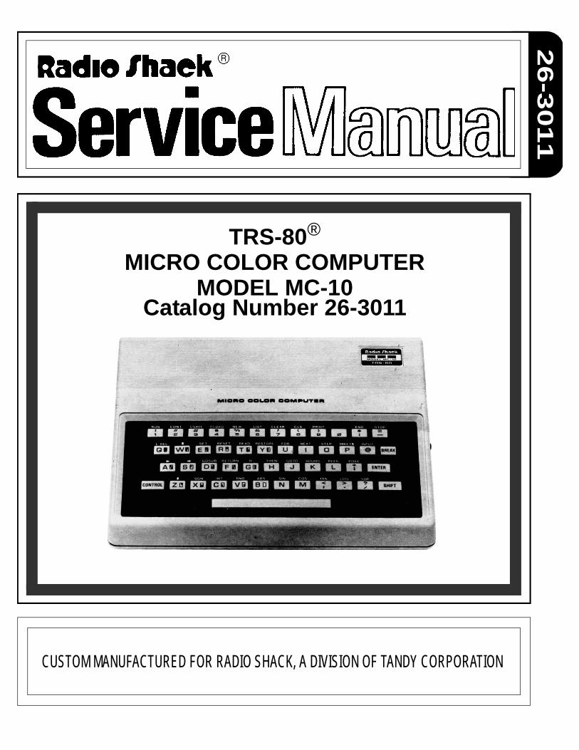
TRS-80®
MICRO COLOR COMPUTERMODEL MC-10
Catalog Number 26-3011
CUSTOM MANUFACTURED FOR RADIO SHACK, A DIVISION OF TANDY CORPORATION
26-3
011

– 2 –
TABLE OF CONTENTS
SECTION PAGENUMBER NUMBER
I SYSTEM DESCRIPTION - - - - - - - - - - - - - - - - - - - - - - - - - - - - - - - - - - - - - - - - - - - - - 3
II SPECIFICATIONS - - - - - - - - - - - - - - - - - - - - - - - - - - - - - - - - - - - - - - - - - - - - - - - - - - 7
III DISASSEMBLY / REASSEMBLY - - - - - - - - - - - - - - - - - - - - - - - - - - - - - - - - - - - - - - - 9
IV THEORY OF OPERATION - - - - - - - - - - - - - - - - - - - - - - - - - - - - - - - - - - - - - - - - - - - 11CPU-6803 - - - - - - - - - - - - - - - - - - - - - - - - - - - - - - - - - - - - - - - - - - - - - - - - - - - - - 12Reset Circuit - - - - - - - - - - - - - - - - - - - - - - - - - - - - - - - - - - - - - - - - - - - - - - - - - - - 12ROM - - - - - - - - - - - - - - - - - - - - - - - - - - - - - - - - - - - - - - - - - - - - - - - - - - - - - - - - - 12Cassette Interface - - - - - - - - - - - - - - - - - - - - - - - - - - - - - - - - - - - - - - - - - - - - - - - 12Detailed Tape Format Information - - - - - - - - - - - - - - - - - - - - - - - - - - - - - - - - - - - 13RS-232C Interface - - - - - - - - - - - - - - - - - - - - - - - - - - - - - - - - - - - - - - - - - - - - - - - 14I/O Connector - - - - - - - - - - - - - - - - - - - - - - - - - - - - - - - - - - - - - - - - - - - - - - - - - - 15Keyboard Interface - - - - - - - - - - - - - - - - - - - - - - - - - - - - - - - - - - - - - - - - - - - - - - 16TV Switch Box - - - - - - - - - - - - - - - - - - - - - - - - - - - - - - - - - - - - - - - - - - - - - - - - - 16Power Supply - - - - - - - - - - - - - - - - - - - - - - - - - - - - - - - - - - - - - - - - - - - - - - - - - - 17VDG - - - - - - - - - - - - - - - - - - - - - - - - - - - - - - - - - - - - - - - - - - - - - - - - - - - - - - - - - 17Device Selection - - - - - - - - - - - - - - - - - - - - - - - - - - - - - - - - - - - - - - - - - - - - - - - - 19System Timing - - - - - - - - - - - - - - - - - - - - - - - - - - - - - - - - - - - - - - - - - - - - - - - - - 19RAM - - - - - - - - - - - - - - - - - - - - - - - - - - - - - - - - - - - - - - - - - - - - - - - - - - - - - - - - - 20Modulator - - - - - - - - - - - - - - - - - - - - - - - - - - - - - - - - - - - - - - - - - - - - - - - - - - - - - 20
V TROUBLESHOOTING - - - - - - - - - - - - - - - - - - - - - - - - - - - - - - - - - - - - - - - - - - - - - - 21
VI PARTS LIST - - - - - - - - - - - - - - - - - - - - - - - - - - - - - - - - - - - - - - - - - - - - - - - - - - - - - 25
VII PRINTED CIRCUIT BOARDS - - - - - - - - - - - - - - - - - - - - - - - - - - - - - - - - - - - - - - - - 30
VIII IC INTERNAL CONNECTIONS - - - - - - - - - - - - - - - - - - - - - - - - - - - - - - - - - - - - - - - 33
IX SCHEMATlC DlAGRAM - - - - - - - - - - - - - - - - - - - - - - - - - - - - - - - - - - - - - - - - - - - - 44
X EXPLODED VlEW - - - - - - - - - - - - - - - - - - - - - - - - - - - - - - - - - - - - - - - - - - - - - - - - - 46
[ Editor’s Note: I would also like to express my thanks to RadioShack for permit-ting the distribution of this manual. I hope you find it useful. I have found a fewtypos and inconsistencies in the Service Manual that I have noted in an italizedfont like this. JMM.]
– 3 –
SECTION I
SYSTEM DESCRIPTION

– 4 –
SYSTEM DESCRIPTION
The MC-10 Micro Color Computer is a fullyexpandable microprocessor system. It is com-posed of a 6803 central processing unit, 4K ofstatic RAM, 8K of Basic ROM, and a 6847 videodisplay generator. The microcomputer is alsointerfaced to a 48-key keyboard and providesthe logic to execute a 1500 Baud cassette inter-face and a RS-232 serial interface. The systemoperates on a common color burst frequencyof 3.579545 MHz. This main clock is divided by4 in the CPU to yield an operating speed of 0.89MHz.
In operation, the 4K of static RAM is sharedbetween the CPU and the video display gene-rator. This time multiplexing is based on theprocessor clock E. The CPU will be grantedaccess to the RAM (upon request) only duringthe high state of E. This allows efficient usageof the RAM with no waiting by the CPU and novisible conflict on the display.
The 6847 VDG provides a display on a TVscreen of 32 characters by 16 rows. It alsoallows a 64 x 32 semigraphics mode with eightcolors. This display utilizes a minimum amountof system RAM (512 bytes).
The final elements of the microcomputer sys-tem are the I/O devices. The MC-10 is interfacedto a 48-key keyboard which generates thecodes for upper and lower case characters,graphics symbols, and single stroke keyboardentry. The computer also provides a 1500 baudcassette interface for fast and reliable data andprogram storage and a limited signal RS-232Cinterface. The RS-232C interface allows either aprinter or a modem to be used with the MC-10.

– 5 –
SYSTEM BLOCK DIAGRAM
– 6 –
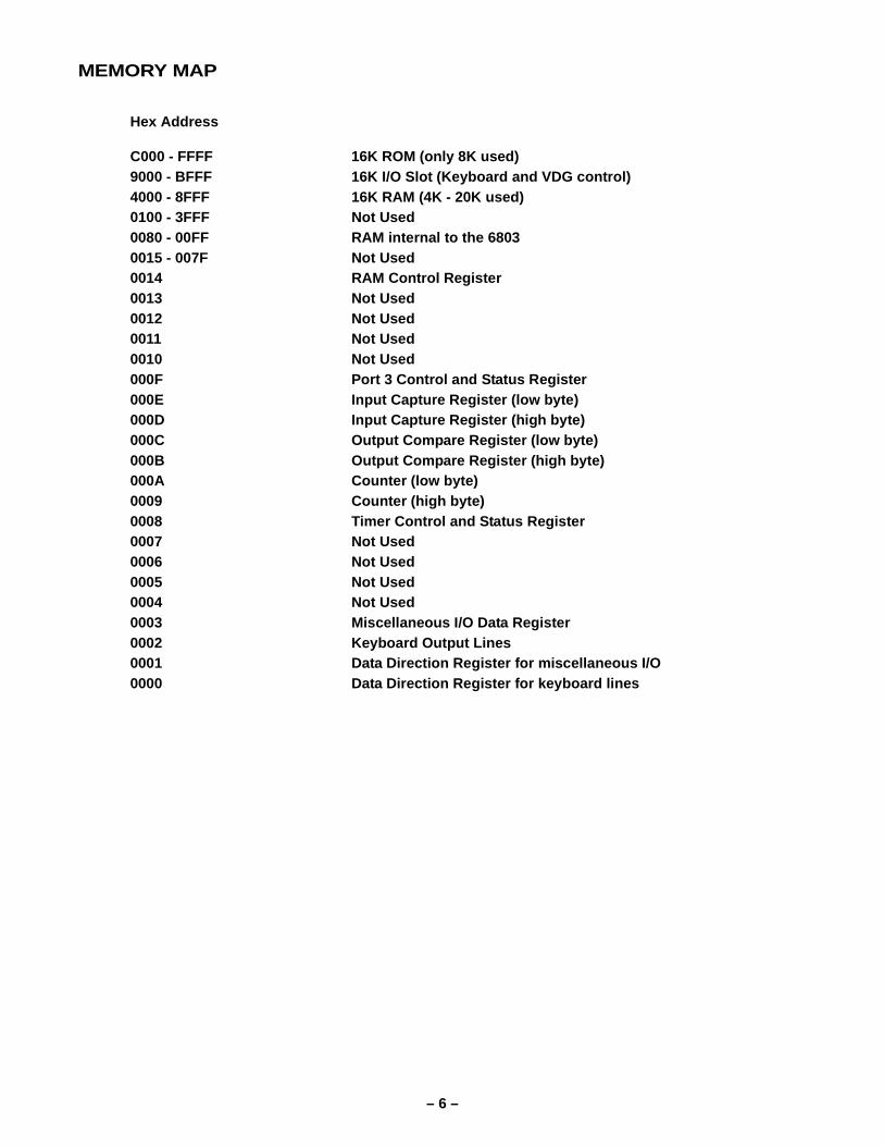
MEMORY MAP
Hex Address
C000 - FFFF 16K ROM (only 8K used)9000 - BFFF 16K I/O Slot (Keyboard and VDG control)4000 - 8FFF 16K RAM (4K - 20K used)0100 - 3FFF Not Used0080 - 00FF RAM internal to the 68030015 - 007F Not Used0014 RAM Control Register0013 Not Used0012 Not Used0011 Not Used0010 Not Used000F Port 3 Control and Status Register000E Input Capture Register (low byte)000D Input Capture Register (high byte)000C Output Compare Register (low byte)000B Output Compare Register (high byte)000A Counter (low byte)0009 Counter (high byte)0008 Timer Control and Status Register0007 Not Used0006 Not Used0005 Not Used0004 Not Used0003 Miscellaneous I/O Data Register0002 Keyboard Output Lines0001 Data Direction Register for miscellaneous I/O0000 Data Direction Register for keyboard lines

– 7 –
SECTION II
SPECIFICATIONS

– 8 –
SPECIFICATIONS
Power SupplyAC/AC adaptor Input 120V/60Hz
Output 8.0V/1.5A 16W
RF Modulator Ch. FC (MHz) Fsc (MHz)For U.S.A./CANADA 3 61.25 +/-0.25 4.5 +/-0.2
4 67.65 4.5
Output Impedance 75 ohmRF Output Terminal RCA jackRF Output Level 1.5 - 2.8 mV at 75 ohm
Central Processing Unit6803 8-bit processorclock speed 0.89 MHz
Memory SizeROM (for BASIC) 8KRAM 4K (expandable up to
20K-external)
Video DisplayCharacter display 512 (32 x 16) upper case
charactersSemi-Graphic display 64 x 32 elementsColor 8 colors - Green, Yellow,
Blue, Red, Buff, Cyan, Magenta, Orange
InterfacePrinter RS232C, 4 pin DINCassette 5-pin DIN 1500 baudBus line 34-pin Cartridge connector
Switch BoxIsolation more than 60 dB
Dimensions8-1/2" x 1-7/8” x 7”
Weight1.75 Ibs (.7875 kilograms)
– 9 –
SECTION III
DISASSEMBLY / REASSEMBLY

– 10 –
DISASSEMBLY
1. Unplug the units from the AC wall outletand disconnect all cables from the rearpanel.
2. Turn the computer over and remove thefour screws from the case bottom. One ofthe screws is located under the warrantyseal in the upper right corner of the casebottom.
3. Turn the computer right side up. Discon-nect the snap locks located on the right andleft side of the case by placing a slottedscrew driver in the groove between the topand bottom cases, approximately 2.7inches from the rear of case. Push in andturn the screwdriver to pop the case apart.
4. Disconnect Keyboard cable from wire con-nector. NOTE: Pull flat wire upward.
5. Remove three screws that fasten the PCBoard to the bottom of the case. Removethe PC Board.
6. Use tweezers to remove eleven clips thatfasten the bottom shield to the P.C. Board.
7. Locate the eight positions where the topshield is soldered to the PC Board. Removethis solder with solder wick or a desolder-ing tool. Bend the protruding edge of theshield upward until it is parallel to the slotand remove top shield.
REASSEMBLY
1. Install the top PC Board shield. Solder theshield to the ground plane at eight points.
2. Install the bottom shield with metal side up.Secure to the PC Board with eleven clips.
3. Install PC Board in bottom of case. Securewith three screws.
4. Install the two keyboard cables in theirrespective connectors. This will be easier ifboth hands are used and you are facingrear of unit. Refasten cable restraints.
5. Join the top and bottom cases and pushthem together at the snap lock positions.This is a tight fit, therefore repositioning ofthe cases may be required.
6. Install four screws in bottom of case.
1. Removal of Top CabinetRemove 4 screws as shown in Figure A.
Figure A
2. Removal of P.C. BoardRemove flat wires of keyboard from con-nector.Remove 3 screws as shown in Figure B.
Figure B
3. Removal of KeyboardRemove 4 screws as shown in Figure C.
Figure C

– 11 –
SECTION IV
THEORY OF OPERATION

– 12 –
CPU-6803
The main component of this microcomputersystem is the 6803 CPU. This is a 40-pin in-tegrated circuit which provides the address,data, and miscellaneous control signals. TheCPU receives the main clock frequency of3.579545 MHz from the modulator assemblyand divides this by 4 to produce an operatingfrequency of 0.89 MHz. This frequency is avail-able as the processor clock E.
This processor chip is designed to be used in aminimum hardware configuration so, I/O linesare provided directly from the CPU chip. In theMC-10 computer these I/O lines are used toaddress the keyboard and to support the cas-sette and RS232 interface.
The 6803 CPU is able to support several differ-ent modes of operation. For the MC-10 the CPUis operating in mode 2. The CPU mode isselected at power-up by the state of lines P20,P21, and P22. P20 and P22 are connected by adiode to Reset so that during power-up theselines are low. P21 is connected to a pull-upresistor so that during power-up it is high.
Mode 2 operates with 128 bytes of internalRAM, a full 16 line address bus and an 8 bitdata bus which is multiplexed with the lowereight address lines. Due to the multiplexedaddress and data bus, two external devices arerequired. A 74LS373 is used to latch theaddress lines. This occurs during the low por-tion of the E clock when the CPU is not access-ing external devices. The latch signal (AS) isprovided by the CPU. The other external deviceis a 74LS245. This bi-directional buffer isrequired to isolate the RAM output lines, whichare providing data to the video display genera-tor during the low portion of the E clock, awayfrom the CPU data bus. This buffer is controlledby the device selection logic.
RESET CIRCUIT
The reset circuit is composed of switch S1diode D9, resistor R24, capacitor C8, and twogates of IC U12. R24 and C8 form a simple timeconstant so that during power up or wheneverthe reset switch is pressed, the reset line willstay low for a few milliseconds before returningto the high state. The reset input to the 6803does not provide hysteresis so the reset signalmust be buffered by U12 before being con-nected to the CPU. The final component of thecircuit is diode D9 which is provided to allowfor rapid cycling of the power switch.
ROM
The MC-10 uses a single 8K x 8 ROM to storethe BASIC operating language. This is locatedin a 16K memory map segment between hexC000 - FFFF. This device is connected directlyto the multiplexed address/data, however anypossible contention is avoided by enabling theROM only during the high cycle of the E clock.
CASSETTE INTERFACE
The cassette interface is composed of an out-put attenuator connected to a CPU output lineand an input zero crossing detector. Most ofthe important cassette parameters are con-trolled by software. However, there is no cas-sette motor relay in the Micro Color Computerand cassette recorder operation must be man-ual.
The cassette format chosen uses a sinewave of2400 or 1200 Hertz to yield a Baud rate of ap-proximately 1500 Baud. In this format, a 0 (orlogic low) is represented by one cycle of 1200Hertz. A 1 (or logic high) is represented by onecycle of 2400 Hertz. A sample of data is shownin Figure 2. A typical program tape would con-sist of a leader of alternating 1’s and 0’s, fol-lowed by one or more blocks of data. A block ofdata is composed of 0 to 255 bytes of data witha checksum, sync byte, and the block length.
The output circuit utilizes a CPU output line toproduce a sinewave of 1200 or 2400 Baud. Thissignal is then attenuated to approximately 1volt and connected to the auxiliary input of thecassette recorder.

– 13 –
DETAILED TAPE FORMAT INFORMATION
tor equal to 1/2 volt. Since the other input isbiased at 1 volt, the comparator output isswitched to the high state. If the AC input fromthe recorder is positive, diode D6 is turned offand the input to the comparator will be at somepoint greater than 1 volt, in which case, thecomparator output will be low.
The input circuit is a zero crossing detector.R12 is a termination resistor for the cassetteoutput. Resistors R16 and R17 are used to biasone input of the comparator at 1 volt. The otherinput is also biased at 1 volt by R15 and theseries combination of R14 and R13. If the ACinput from the recorder goes negative, diodeD6 turns on and sets the input to the compara-
the comparator. The final portion of the cas-sette circuit is capacitor C7 which is used toisolate noise from the cassette cable.
The comparator output is open-collector sopullup resistor R19 is provided to generate aTTL signal. R18 is used to prevent oscillation of
Figure 2. Sample Data of Cassette FormatThis is shown inverted to indicate possible phase inversion by the tape recorder.
0
0
1
1
0
0
0
0
1
1
1
1
1
1
0
0
REFERENCE SQUARE WAVE
COMPUTER MEMORY DATA
D/A OUTPUT
INPUT TO TAPE
OUTPUT FROM TAPE
INPUT TO THE PIA
DATA STOREDIN MEMORY
4.6v
0v
1v0v
2.5v
0v2.5v
5v
0v
The End of File block is a standard block with alength of 0 and the block type equal to FFH. TheNamefile block is a standard block with alength of 15 bytes (0FH) and the block typeequals 00H. The 15 bytes of data provide infor-mation to BASIC and are employed as de-scribed below:1. Eight bytes for the program name2. One file type byte - 00H = BASIC, 01H =
Data, 02H = Machine Language3. One ASCII flag byte - 00H = Binary, FFH =
ASCII4. One Gap flag byte - 01H = Continuous, FFH
= Gaps5. Two bytes for the start address of a
machine language program6. Two bytes for the load address of a
machine language program
The standard MC-10 tape is composed of thefollowing items:1. A leader consisting of 128 bytes of hex 552. A Namefile block3. A blank section of tape approximately
equal to 0.5 seconds in length; this allowsBASIC time to evaluate the Namefile.
4. A second leader of 128 bytes of Hex 55 5. One or more Data blocks6. An End of File block
The block format for Data blocks, NamefileBlocks, or an End of File block is as follows:1. One leader byte - 55H2. One sync byte - 3CH3. One block type byte — 01H = Data, FFH =
End of File, 00H - Namefile4. One block length byte - 00H to FFH 5. Data - 0 to 255 bytes6. One checksum byte - the sum of all the data
plus block type and block length7. One leader byte - 55H
– 14 –
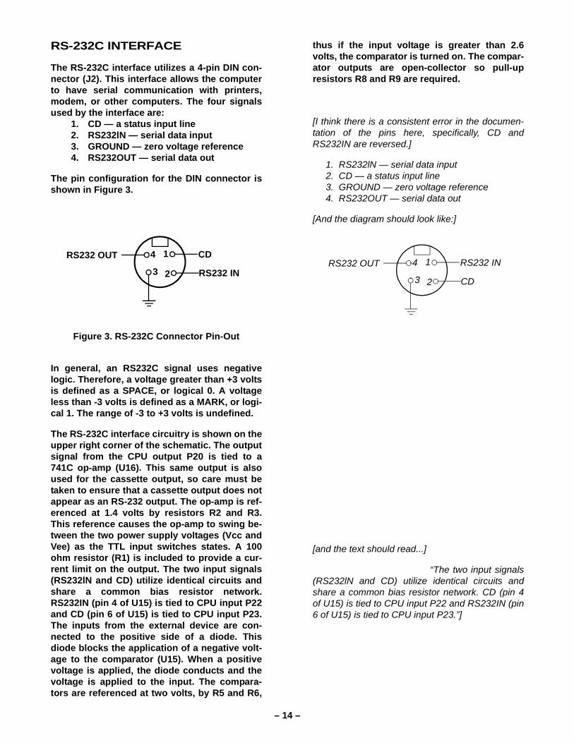
RS-232C INTERFACE
The RS-232C interface utilizes a 4-pin DIN con-nector (J2). This interface allows the computerto have serial communication with printers,modem, or other computers. The four signalsused by the interface are:
1. CD — a status input line2. RS232lN — serial data input3. GROUND — zero voltage reference4. RS232OUT — serial data out
The pin configuration for the DIN connector isshown in Figure 3.
Figure 3. RS-232C Connector Pin-Out
In general, an RS232C signal uses negativelogic. Therefore, a voltage greater than +3 voltsis defined as a SPACE, or logical 0. A voltageless than -3 volts is defined as a MARK, or logi-cal 1. The range of -3 to +3 volts is undefined.
The RS-232C interface circuitry is shown on theupper right corner of the schematic. The outputsignal from the CPU output P20 is tied to a741C op-amp (U16). This same output is alsoused for the cassette output, so care must betaken to ensure that a cassette output does notappear as an RS-232 output. The op-amp is ref-erenced at 1.4 volts by resistors R2 and R3.This reference causes the op-amp to swing be-tween the two power supply voltages (Vcc andVee) as the TTL input switches states. A 100ohm resistor (R1) is included to provide a cur-rent limit on the output. The two input signals(RS232lN and CD) utilize identical circuits andshare a common bias resistor network.RS232IN (pin 4 of U15) is tied to CPU input P22and CD (pin 6 of U15) is tied to CPU input P23.The inputs from the external device are con-nected to the positive side of a diode. Thisdiode blocks the application of a negative volt-age to the comparator (U15). When a positivevoltage is applied, the diode conducts and thevoltage is applied to the input. The compara-tors are referenced at two volts, by R5 and R6,
4 1
23
CD
RS232 IN
RS232 OUT
thus if the input voltage is greater than 2.6volts, the comparator is turned on. The compar-ator outputs are open-collector so pull-upresistors R8 and R9 are required.
[I think there is a consistent error in the documen-tation of the pins here, specifically, CD andRS232IN are reversed.]
1. RS232lN — serial data input 2. CD — a status input line 3. GROUND — zero voltage reference 4. RS232OUT — serial data out
[And the diagram should look like:]
[and the text should read...]
“The two input signals(RS232lN and CD) utilize identical circuits andshare a common bias resistor network. CD (pin 4of U15) is tied to CPU input P22 and RS232IN (pin6 of U15) is tied to CPU input P23.”]
4 1
23
RS232 IN
CD
RS232 OUT
– 15 –
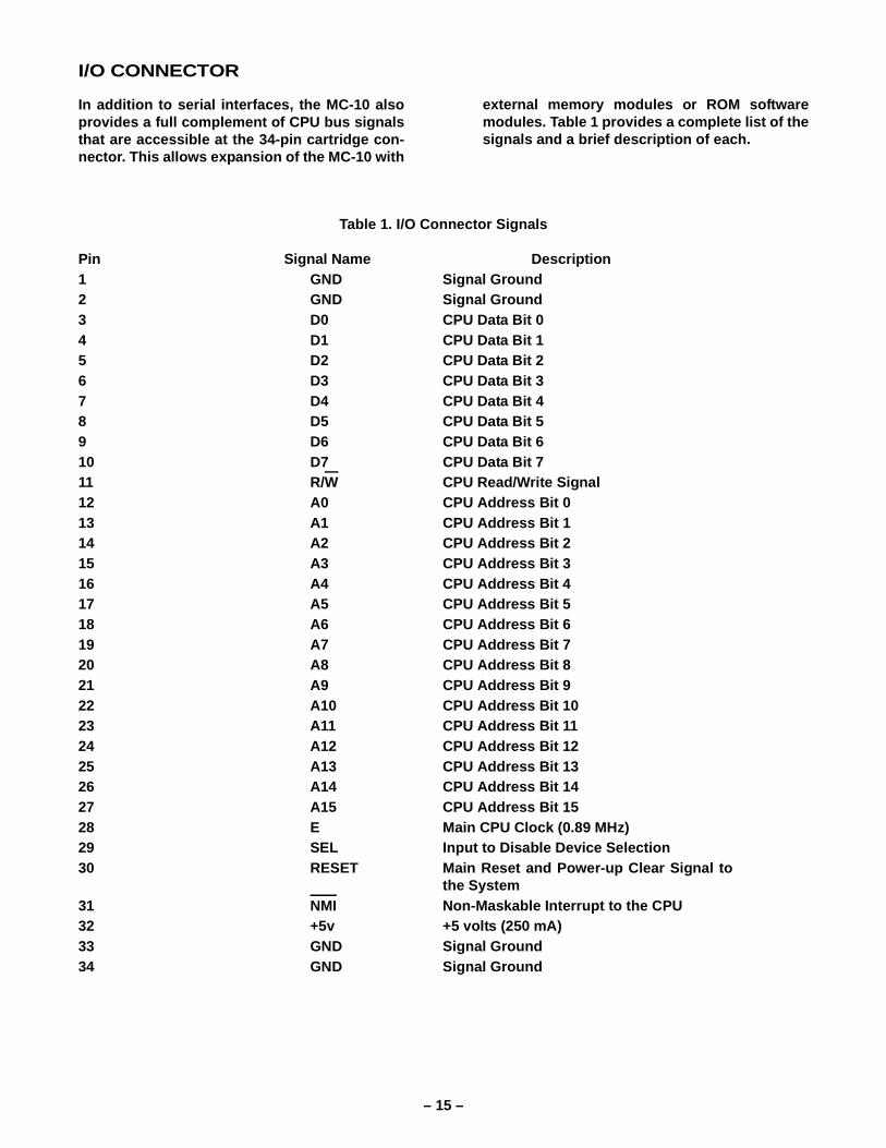
I/O CONNECTOR
Table 1. I/O Connector Signals
Pin Signal Name Description1 GND Signal Ground2 GND Signal Ground3 D0 CPU Data Bit 04 D1 CPU Data Bit 15 D2 CPU Data Bit 26 D3 CPU Data Bit 37 D4 CPU Data Bit 48 D5 CPU Data Bit 59 D6 CPU Data Bit 610 D7 CPU Data Bit 711 R/W CPU Read/Write Signal12 A0 CPU Address Bit 013 A1 CPU Address Bit 114 A2 CPU Address Bit 215 A3 CPU Address Bit 316 A4 CPU Address Bit 417 A5 CPU Address Bit 518 A6 CPU Address Bit 619 A7 CPU Address Bit 720 A8 CPU Address Bit 821 A9 CPU Address Bit 922 A10 CPU Address Bit 1023 A11 CPU Address Bit 1124 A12 CPU Address Bit 1225 A13 CPU Address Bit 1326 A14 CPU Address Bit 1427 A15 CPU Address Bit 1528 E Main CPU Clock (0.89 MHz)29 SEL Input to Disable Device Selection30 RESET Main Reset and Power-up Clear Signal to
the System31 NMI Non-Maskable Interrupt to the CPU32 +5v +5 volts (250 mA)33 GND Signal Ground34 GND Signal Ground
external memory modules or ROM softwaremodules. Table 1 provides a complete list of thesignals and a brief description of each.
In addition to serial interfaces, the MC-10 alsoprovides a full complement of CPU bus signalsthat are accessible at the 34-pin cartridge con-nector. This allows expansion of the MC-10 with
– 16 –
KEYBOARD INTERFACE
TV SWITCH BOX
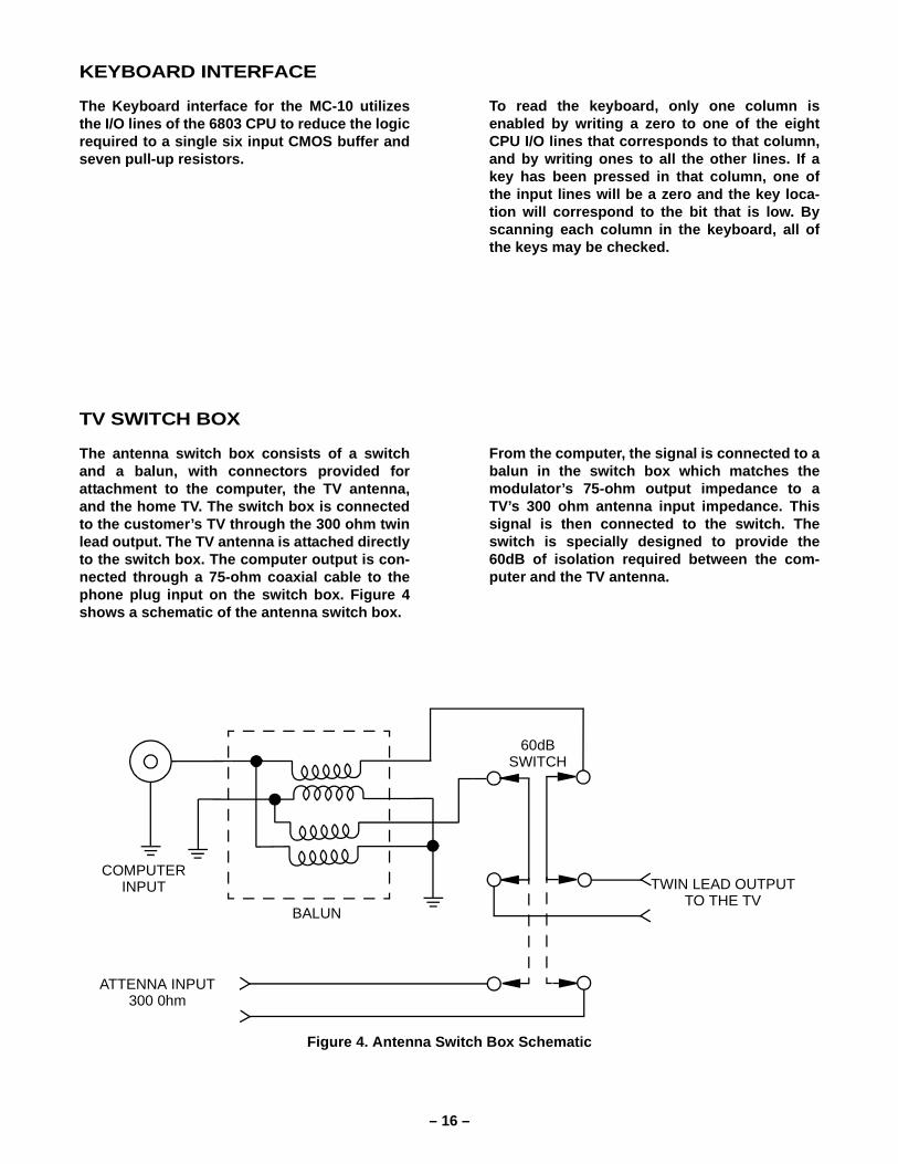
Figure 4. Antenna Switch Box Schematic
To read the keyboard, only one column isenabled by writing a zero to one of the eightCPU I/O lines that corresponds to that column,and by writing ones to all the other lines. If akey has been pressed in that column, one ofthe input lines will be a zero and the key loca-tion will correspond to the bit that is low. Byscanning each column in the keyboard, all ofthe keys may be checked.
The Keyboard interface for the MC-10 utilizesthe I/O lines of the 6803 CPU to reduce the logicrequired to a single six input CMOS buffer andseven pull-up resistors.
From the computer, the signal is connected to abalun in the switch box which matches themodulator’s 75-ohm output impedance to aTV’s 300 ohm antenna input impedance. Thissignal is then connected to the switch. Theswitch is specially designed to provide the60dB of isolation required between the com-puter and the TV antenna.
The antenna switch box consists of a switchand a balun, with connectors provided forattachment to the computer, the TV antenna,and the home TV. The switch box is connectedto the customer’s TV through the 300 ohm twinlead output. The TV antenna is attached directlyto the switch box. The computer output is con-nected through a 75-ohm coaxial cable to thephone plug input on the switch box. Figure 4shows a schematic of the antenna switch box.
COMPUTERINPUT
60dB
ATTENNA INPUT
BALUN
300 0hm
SWITCH
TWIN LEAD OUTPUTTO THE TV

– 17 –
POWER SUPPLY
The MC-10 power supply utilizes an externalpower pack to supply 8 VAC at 1.5 amps. Thisinput AC voltage is connected through thepower switch to the bridge rectifier. The MC-10operates primarily on +5 volts, so the negativeoutput of the bridge is grounded to provide alarger current capability to the positive supply.The output from the bridge is filtered by C1 andC5 and is connected to the +5 volt regulator.The regulator provides +5 volts at a maximumof 1.5 amps to the digital circuitry.
A small amount of negative voltage is requiredto the RS-232 output op-amp. This current issupplied by the simple circuit composed of D2,D3, C3, C4, and C32. This circuit operates byusing capacitor C3 for isolation from the pri-mary bridge circuit. Then the negative voltageis rectified by D2 and D3. The negative supplyvoltage is then filtered by C4 and C32 beforebeing connected to U16. This is an unregulatedoutput. However, when coupled with the outputfrom the main bridges, it provides a larger dif-ferential voltage (that is the source of the posi-tive op-amp voltage) with no detrimental effectson the operation of the op-amp.
VDG
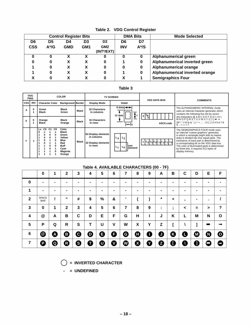
The video interface function in the MC-10 isperformed by the MC6847. This is a flexiblevideo display generator that will produce ninecolors (eight colors and black), an alphanu-meric display mode, and several high resolu-tion graphics modes.
In the MC-10 the VDG is interfaced to 4K ofstatic RAM and the mode control inputs arecontrolled by a 74LS174 register. However, theonly modes of operation which are supportedby the machine are the alphanumeric mode andthe alpha semigraphic-4 mode. Table 4 lists allof the alphanumeric characters which may bedisplayed by the VDG along with the hex codewhich will produce the character. Table 2 liststhe required control bit values to produce theMC-10 display modes.
In the MC-10 the 4K of RAM is shared betweenthe CPU and video display generator. This isaccomplished by providing buffers betweenthe address lines (U5 and U6) the data line (U7),and synchronizing the operation of the VDG tothe CPU.
Normally the three buffers are disabled so thatthe VDG address is being supplied to the RAMand the RAM data is supplied to the VDG. How-ever, during a CPU access to the RAM, thethree buffers are enabled and the MS* line isused to disable the address lines of theMC6847. This provides the CPU address to theRAM chips and allows a CPU read or writecycle to occur.
– 18 –
Table 2. VDG Control Register
Table 3
Table 4. AVAILABLE CHARACTERS (00 - 7F)
Control Register Bits DMA Bits Mode SelectedD6 D5 D4 D3 D2 D6 D7
CSS A*/G GMD GM1 GM2(INT*/EXT)
INV A*/S
0 0 X X 0 0 0 Alphanumerical green0 0 X X 0 1 0 Alphanumerical inverted green1 0 X X 0 0 0 Alphanumerical orange1 0 X X 0 1 0 Alphanumerical inverted orangeX 0 X X 0 X 1 Semigraphics Four
0 1 2 3 4 5 6 7 8 9 A B C D E F
0 - - - - - - - - - - - - - - - -
1 - - - - - - - - - - - - - - - -
2 SPACE BAR ! “ # $ % & ‘ ( ) * + , - . /
3 0 1 2 3 4 5 6 7 8 9 : ; < = > ?
4 @ A B C D E F G H I J K L M N O
5 P Q R S T U V W X Y Z [ \ ]
6
7
VDGPINS
CSS INV Character Color Background Border Display Mode Detail
COLOR TV SCREENVDG DATA BUS COMMENTS
0 0 Green Black 32 Characters1 Black Green in columnsBlack
0 0 Orange Black 16 Characters1 Black Orange in rowsBlack
64 Display elements in columns
32 Display elements in rows
Blackx x
Lx C2 C1 C0 Color0 x x x Black1 0 0 0 Green1 0 0 1 Yellow1 0 1 0 Blue1 0 1 1 Red1 1 0 0 Buff1 1 0 1 Cyan1 1 1 0 Magenta1 1 1 1 Orange
L L3 2
L L1 0oneelement
12 dots
8 dots
5
7
1 C C C L L L L 2 1 0 3 2 1 0
0
ASCII code
INV
The ALPHANUMERIC INTERNAL modeuses an internal character generator whichcontains the following five dot by sevendot characters @ A B C D E F G H I J K LM N O P Q R S T U V W X Y Z [ \ ] SP ! ” # $ % & ‘ ( ) * + , - . / 0 1 2 3 4 5 6 7 89 : ; < = > ?
The SEMIGRAPHICS FOUR mode usesan internal “coarse graphics” generatorin which a rectangle (eight dots by twelvedots) is divided into four equal parts. Theluminance of each part is determined bya corresponding bit on the VDG data bus.The color of illummated parts is determinedby three bits. It requires 512 bytes ofdisplay memory.
@ A B C D E F G H I J K L M N O
P Q R S T U V W X Y Z [ \ ]
= INVERTED CHARACTER
- = UNDEFINED

– 19 –
DEVICE SELECTION
SYSTEM TIMING
Figure 5
allows an external device to change the MC-10memory map. Also, the disable signal for thememory write is ORed with A12 to prevent acomplete overlap of the 4K of RAM into the 16Kmemory map segment.
From the output of the 74LS155 the IY1 outputis used to switch the tri-state controls for thememory address and data buffers. The IY2 out-put is ORed with R/W and inverted R/W to pro-vide a write pulse to the VDG control register(U8) and a read enable for the keyboard inputbuffer. The final output (IY3) is used to selectthe ROM chip.
A 74LS155 is used along with four OR gatesand two inverters to provide device selection inthe MC-10. The 74LS155 uses A15 and A14 todivide the memory map into four 16K seg-ments. The bottom 16K segment is not usedexternally to the CPU. The next 16K segment isused for system RAM. The third 16K segment isused to read the keyboard and to write to theVDG control register. The final 16K is reservedfor system ROM.
Both sections of the LS155 are used so that allof the device selects may be gated with E, whilethe CPU write signal for the RAMs is gated withwindow* (U18 pin 6). The disable inputs to the74LS155 are tied through an inverter to the car-tridge connector and to a pull-up resistor. This
Internal to the CPU chip, the main clock fre-quency is divided by 4 to produce the proces-sor clock E. This clock is used to synchronizeall system operations to the CPU. Figure 5shows the main clock and timing signals usedin the MC-10.
The main clock frequency of 3.579545 MHz isproduced by the oscillator circuit in the modu-lator. This clock is buffered by one gate of U12before being connected to the CPU and to theclock synchronization circuitry.
3.579545 MHz CLK
E CLOCK
AS U1-39
WIN U18-6

– 20 –
The MC6847 (VDG) has access to the RAM dur-ing the low portion of the E clock. Also duringthe low portion of E, the signal AS is used tolatch the address lines in the latch (U2). Duringthe high portion of E, all CPU address and datalines are valid and any accesses to the RAM orROM occur during this time.
The signal window is used for two purposes.The first usage is to gate the write signal. The2K x 8 static RAM requires setup and hold timeon the address and data line, during a writecycle. The address and data lines are both validfor the high portion of the E clock. By gatingthe write pulse with window, a safety margin iscreated, so that the write pulse will never golow while the address or data is changing.
The second usage of the signal window is forsynchronization of the VDG and the CPU. Thetwo devices must be synchronized to allowboth the CPU and the VDG to use the systemRAM with no conflict. This has been accom-plished in the MC-10 by forcing the VDG tolatch data at the end of the low portion of the Eclock. To do this, low transition of the signalHS* is only allowed to happen during the activeportion of the signal window. If HS* occurs dur-ing the window, the latching of data will occurat the end of the low portion of the E clock.
RAM
The MC-10 uses two 2K x 8 static RAM chips fora total internal memory of 4K. The RAM chipsreceive their address lines from either theMC6847 (VDG) or the CPU. This switching isaccomplished by tri-state buffers which arecontrolled by the MS* line. The individual RAMchip is selected by VA11, the 12th address line,and since the OE* input is grounded, one RAMis always enabled. The WE* line is generated bythe CPU address decoding logic, and is highexcept when the CPU is writing to RAM.
MODULATOR
The outputs from the MC6847 are connecteddirectly to the modulator. The modulator unit isbuilt around the MC1372. This is a linear inte-grated circuit which is designed to interface tothe MC6847 and produce an RF output for con-nection to the TV. Figure 6 shows a block dia-gram of the MC1372 chip.
The 3.579545 MHz crystal and associated com-ponents are connected between pins 1 and 2.This provides the color burst frequency and themain clock for the MC-10. The duty cycle inputis left unconnected to produce a 50% dutycycle clock.
The other inputs to the MC1372 are the lumi-nance input, øA, øB, and the color referencevoltage input. All of these inputs are connecteddirectly to the MC6847 chip.
The chroma modulator output is filtered by anR-C network between pins 8 and 10 of theMC1372. Also the 4.5 MHz frequency modulatedsound signal is AC coupled in at pin 10. Thesound input to the modulator is used to fre-quency modulate the 4.5 MHz oscillator com-posed of Q1 and the associated circuitry.
The channel selection for the modulator is per-formed by the tank circuit between pins 13 and14 of the MC1372. This circuit allows the RFoutput to be switched from channel 3 to 4 by anexternal switch input.
The final RF output of the modulator is avail-able at pin 12 of the MC1372. However, beforethis signal is connected to the output jack, avestigial sideband filter must be used to sup-press unwanted harmonics of the signal. Thisfilter is shown in the schematic as the thirteenpassive components before the RF output.
Figure 6. MC1372 Block Diagram
11
4 3 7 6 13 14
5 9 12
10
8
2
1
CHROMINANCEINPUT
CHROMAMODULATOROUTPUT
RFMODULATOROUTPUT
LUMINANCEINPUT
COLOR BINPUT
COLOR AINPUT
COLORREFERENCEINPUT
CLOCKOUTPUT
OSCILLATORINPUT
DUTY CYCLEADJUST
V
GROUND
CC
RF TANK
LAG
LAG
CHROMAMODULATOR
B
CHROMAMODULATOR
A
RFMODULATOR
RFOSCILLATOR
CHROMINANCEOSCILLATOR
andCLOCKDRIVER

– 21 –
SECTION V
TROUBLESHOOTING

– 22 –
TROUBLESHOOTING
Problems with the MC-10 may be separated intotwo major areas - I/O problems and dead com-puter problems. If the computer will display thesign-on message, then a fairly simple set oftesting procedures may be used to isolate theproblem. If, however, the computer displaysrandom characters on the screen or has no dis-play, then a major failure has occurred.
In the case of a major failure, the first thing tocheck is the +5-volt power supply. If the voltagelevel is off by more than 10%, then the powersupply is the problem. Refer to the Power Sup-ply section for hints on how to isolate the prob-lem.
If the power supply has a proper +5 volts out-put, then check the clock output from the mod-ulator at U12 pin 13. If the clock is oscillating atthe proper frequency, and you have no display,the problem is in the video area. Refer to thesection on the video interface for hints on fix-ing this problem.
If the MC-10 displays garbage on the screen,then some problem is causing a failure of theCPU. At this point you will have to remove thetop and bottom shield. After you have removedthe two shields, test the operation of the MC-10to be sure that the problem was not a short tothe shield.
With both of the shields removed, check theaddress and data lines of the 6803. After thereset switch has been pressed, check for indi-cations that the CPU is operating. If the CPUshows no signs of activity, then one of theinput signals is preventing the CPU from oper-ating or the CPU is bad.
If the CPU is operating, then the most likelyproblems are a memory or buffer chip failure ora short on the address or data bus. In this caseyou will have to methodically check theaddress and data lines, while looking for a linethat shows a problem.
In the case of a simple I/O problem, please referto the appropriate interface section discussion.
VIDEO INTERFACE
Almost all of the work for the video interface isperformed by the VDG (U11 - MC6847). There-fore, this chip is the most likely source of avideo problem. However, it is always a goodidea to isolate the source of a problem beforetrying to desolder chips.
If the problem is no picture or a distorted pic-ture, then a new switch box and cable shouldbe tried. If you still do not have a picture, thenuse an oscilloscope to look at U11 pin 28. Youshould have a video signal at this point. If youdo not have a video signal, check +5 volts (pin17) and the 3.579 MHz clock (pin 33) , if youhave both of these inputs and no video out,then U11 is bad.
If you have a video signal at pin 28, but no pic-ture on your TV, then there could be a problemwith the modulator. Check the +5-volt inputbefore replacing the modulator.
The only other type of video failure which canoccur in the MC-10 is the loss of synchroniza-tion with the CPU which will cause excessglitches on the screen. If this occurs, then thecircuitry composed of U18 and U19 is failing.
KEYBOARD INTERFACE
The keyboard interface is composed of oneresistor pack and one IC (U14). A keyboard fail-ure will usually be caused by a mechanical fail-ure of the keyboard, or a short or open in thecable. Mechanical failures will usually be onlyone or two isolated keys failing. Cable failureswill cause an entire keyboard row or column tofail.
– 23 –
RS-232 INTERFACE
The RS-232 interface uses three simple levelconverter circuits. Isolating the problem will bean easy job of comparing the input to the out-put.
Connect a DIN-type plug to the serial I/O jack toshort together pins 1, 2, and 4. Now, type in thefollowing test program:
5 POKE 3,1 10 FOR X=0 TO 10: NEXT X 15 POKE3,0 20 FOR X=0 TO 10: NEXT X 25 GOTO 5
Run the program and check pin 2 of U16; aswitching TTL waveform should be present. Pin6 of U16 should have the same waveformexcept that it will be switching from +Vcc to -Vcc (the supply voltages of pins 4 and 7 ofU16). Also check pins 4 and 6 of U15. Thesepins have the same waveform switching from 0to +Vcc. The outputs of U15, pins 1 and 2should show the original TTL signal.
CASSETTE INTERFACE
If you are having problems with the cassettecircuit, short together pins 4 and 5 of the cas-sette DIN plug. Next run the program listed forthe RS-232 interface test. The output pin isshared between RS-232 and cassette, so thistest program will produce a switching TTLwaveform on the output.
The output circuit is a simple attenuator, so thelikely failure here should be a short to ground.The output on pin 5 of the DIN connectorshould be switching for 0 to +1 volt.
The input circuit is a zero crossing detector. Itshould convert the cassette signal back to theoriginal TTL waveform at pin 13 of U15.
POWER SUPPLY
The power supply circuit in the MC-10 has aminimum component count so that a failureshould be readily identifiable.
The first place to check if the computer has no+5-volt supply voltage is the output of the regu-lator. With the power pack unplugged, measurethe resistance between the +5 output and
ground. If this shows zero resistance, the prob-lem is a short to ground.
If the +5 output is not shorted, check the volt-age with the power pack plugged in. Youshould have 8 VAC at the power ON-OFFswitch. If this looks good, check the input tothe regulator. Here you should see a full waverectified voltage of 10 volts DC. If you do not,one of the following components could be bad:D1; CI [C1] or C5; U15, U16, or U17.
The only major remaining component is the +5-volt regulator. If the regutator is receiving theproper input voltage, and there is no +5 volts,the regulator chip is bad.
Also, there is a simple circuit to supply anunregulated negative voltage to the RS-232interface. If you are missing the negative volt-age but the +5 volts is OK, then one of thediodes or the capacitors has failed.
MODULATOR
If clock does not appear at TP 2, there could bea problem with the modulator.
Check the +5 volts (pin 11 of MC1372) and the3.579 MHz clock (pin 1 of MC1372).
If you cannot see the 3.579 MHz clock, checkparts connected to pin 1 and pin 2 (R1, C2, C3,X1) .
If the 3.579 MHz clock is OK but picture is dis-torted, try to tune TV set by adjusting fine tun-ing.
If picture is distorted even after fine turningadjustment, replace modulator unit if you donot have Spectrum Analyzer.
If you have a spectrum analyzer, you can adjustinside of modulator.
Remove the modulator first.
Refer to disassembly instruction on page 10and locate the four positions where modulatoris soldered to P.C. Board. Remove this solderwith solder wick or desoldering tool.
Bend the protruding edge of modulator until itis parallel to the slot and remove modulator.

– 24 –
ADJUSTMENT OF VSB (vestigial side band)FILTER
Make Connection according to Figure 7
Figure 71. Adjust marker of tracking generator at
61.25 MHz (marker - 2)2. Adjust L102 so lower side band peak point
meets 61.25 MHz (marker - 2)3. Adjust marker of tracking generator at
72.15 MHz (marker - 3)4. Adjust L103 so higher side peak point
meets 72.15 MHz (marker - 3)5. Repeat steps 1 to 4 until lower and higher
side band peaks agree with 61.25 MHz(marker - 2) and 72.15 MHz (marker - 3)Refer to Figure 8
6. Adjust L101 so that filter characteristic of -1dB stays about within 12 MHz.
7. Adjust marker point of tracking generatorat 57 MHz (marker - 1) and check the leveldifference between 61.25 MHz (lower sidepeak point - marker 2) and 57 MHz (marker -1) is more than 20 dB.
Figure 8
ADJUSTMENT OF VIDEO CARRIER FRE-QUENCY
Prepare switch, 0.01 µF capacitor and 2.2K ohmresistor and 75 ohm coaxial cable with RCAand 50/75 ohm converter.
Make connection according to Figure 9.1. Set switch to CH 4.2. Adjust T102 core so that frequency counter
of spectrum analyzer shows 67.65 MHz3. Set switch to CH 3.4. Adjust trimmer capacitor of C113 so that
frequency counter of spectrum analyzershows 61.25 MHz.
12
IC1
0.01
C117
C116
L102 L103
TRACKINGGENERATOR
INPUT
RF OUT
RCAJACK
75Ω COAXIALCABLE
L101
50/75Ω ImpedanceOUT
SPECTRUMANALYZER
1 dB
2 dB
20 d
B
12 MHz
57 61.25 72.15 (MHz)Freq.
3
1
2
Figure 9
ADJUSTMENT OF SOUND CARRIER FREQUENCY
Figure 10
Prepare capacitor of 470 µF [pF] and make con-nection according to Figure 10.
Adjust T101 core so that freq. counter shows4.500 MHz.
ADJUSTMENT OF CHROMATIC FREQUENCY
Make connection according to Figure 11.
Adjust trimmer capacitor C102 so that freq.counter shows 3.579545 MHz.
Figure 11
Note: On actual board, unit of hundred of thereference numbers is omitted. Ex. L102 ismarked “L2.”
MDV - 1
CH. Select
RF Out
Luminance In
Sound In
DC PowerSupply
CH. 4
0.01 CH. 3
75Ω CoaxialCable
50/75ΩImpedance
5 ± 0.1V
SPECTRUMANALYZER
Video Carrier
Sound Carrier
Freq. (MHz)
4.5 4.5
T101
R103 IC1
470 pF
Q1
SoundIn
Frequency Counter
10
0.0015 ± 0.1VMDV-1 CLK
OUT
Freq.Counter
RegulatedD.C. PowerSupply

– 25 –
SECTION VI
PARTS LIST

– 26 –
PRINTED CIRCUIT BOARD PARTS
CAPACITORS
DIODES
CORE
CONNECTORS
Ref.No. Value (µF) Voltage (V) Tolerance ( %) R/S Part No. Material
C1 4700 16 ±20 Radial ElectrolyticC2 10 25 ±20 Radial ElectrolyticC3/4 100 16 ±20 Axial ElectrolyticC5 0.1 25 ±20 Radial CeramicC6 0.0022 50 +80/-20 Radial CeramicC7 0.022 50 +80/-20 Radial CeramicC8 4.7 50 ±20 Radial ElectrolyticC9~12 0.022 50 +80/-20 Radial CeramicC13 0.1 25 ±20 Radial CeramicC14~20 0.1 50 ±5 Radial M-Plastic CapacitorC21/22 0.022 50 +80/-20 Radial CeramicC23 0.022 16 ±30 Axial CeramicC24~26 0.022 50 ±80/-20 Radial CeramicC27 0.1 25 ±20 Radial CeramicC28 0.022 50 +80/-20 Radial CeramicC29 0.022 16 ±30 Axial CeramicC30~32 0.022 50 +80/-20 Radial CeramicC33 150P 50 ±5 Radial Ceramic
Ref. No. Description R/S Part No. Manufacture
D1 SIRBA10 RECTIFIER SHINDENGEND2/3 10E1 or SI DIODE
SR1K-2 SI DIODENIHONINTER or UNIZON
D4~9 1N4148 SI DIODE HITACHI or ITT
Ref. No. Description R/S Part No. Mfr’s Part No.
FB1~5 CORE φ3.5 x φ1.3 x 5 or BL01RN1-A61
588010050A 588010060A
Ref. No. Description R/S Part No. Mfr’s Part No.
J1 5P DIN (For CASSETTE I/O) 193410030AJ2 4P DIN (For SERIAL I/O) 193410020AJ3 POWER JACK 196610020AJ4 WIRE CONNECTOR 193904400AJ5 WIRE CONNECTOR 193904400A

– 27 –
RESISTORS
SWITCHES
INTEGRATED CIRCUITS
Ref.No. Value (ohms) Wattage Tolerance ( %) R/S Part No. Material
R1 100 1/2 ±5 CarbonR2 3.9K 1/6 ±5 CarbonR3 1.5K 1/6 ±5 CarbonR4 10K 1/4 ±5 CarbonR5 15K 1/4 ±5 CarbonR6/7 10K 1/4 ±5 CarbonR8/9 4.7K 1/4 ±5 CarbonR10 75K 1/6 ±5 CarbonR11 24K 1/6 ±5 CarbonR12 220 1/4 ±5 CarbonR13 8.2K 1/4 ±5 CarbonR14 6.8K 1/4 ±5 CarbonR15/16 56K 1/4 ±5 CarbonR17 15K 1/4 ±5 CarbonR18 1.5M 1/4 ±5 CarbonR19 4.7K 1/4 ±5 CarbonR20 10K x 8 1/4 ±5 Resistor ArrayR21 4.7K 1/4 ±5 CarbonR22/23 4.7K 1/6 ±5 CarbonR24 100K 1/4 ±5 CarbonR25 4.7K 1/4 ±5 CarbonR26 100K 1/4 ±5 Carbon
Ref. No. Description R/S Part No. Mfr’s Part No.
S1 RESET SW 187010040AS2 POWER SW 183110240AS3 CHANNEL SW 183110280A
Ref. No. Description R/S Part No. Mfr’s Part No.
U1 MC6803G or (MCU) HD6803P
MOTOROLA HITACHI
U2 SN74LS373N or (D-LATCH) MB74LS373M
MOTOROLA FUJITSU
U3 MB8364M (MASK ROM) FUJITSUU4 SN74LS155N or (DECODER)
MB74LS155M orHD74LS155P
MOTOROLA FUJITSUHITACHI
U5/6 SN74LS367AN or (DRIVER)MB74LS367AM orHD74LS367AP
MOTOROLA FUJITSUHITACHI
U7 SN74LS245N or (TRANSCEIVER)MB74LS245M
MOTOROLA FUJITSU

– 28 –
Ref. No. Description R/S Part No. R/S Part No. Mfr’s Part No.
U8 SN74LS174N or (D-TYPE F.F) MB74LS174M or HD74LS174P
MOTOROLA FUJITSU HITACHI
U9/10 µPD4016C-1 or (STATIC RAM) µPD4016D-1 or MB8128-15P or MSM2128-20RS
NEC NEC FUJITSU OKI
U11 MC6847P (VDG) MOTOROLAU12 SN74LS14N or (INVERTER)
MB74LS14M or HD74LS14P
MOTOROLA FUJITSU HITACHI
U13 SN74LS32N or (OR-GATE) MB74LS32M or HD74LS32P
MOTOROLA FUJITSU HITACHI
U14 MC14503BCP or (BUFFER) HD14503BP or µPD4503BC or MSM4503RS
MOTOROLA HITACHI NEC OKI
U15 LM339N or (COMPARATOR) µPC339C
MOTOROLA NEC
U16 MC1741CP1 or (OP AMP) HA17741PS
MOTOROLA HITACHI
U17 MC7805CT or (VOLTAGE REGULATOR) NJM7805A or µPC7805H
MOTOROLA JRC NEC
U18 SN74LS74AN or (D-F.F) MB74LS74AM or HD74LS74AP
MOTOROLA FUJITSU HITACHI
U19 SN74LS76AN or (JK-F.F) MB74LS76AM or HD74LS76P
MOTOROLA FUJITSU HITACHI
U20 SN74LS32N or (OR-GATE) MB74LS32M or HD74LS32P
MOTOROLA FUJITSU HITACHI

– 29 –
EXPLODED VIEW PARTS LIST
MISCELLANEOUS PARTS LIST
Ref. No. Description R/S Part No. R/S Part No. Mfr’s Part No.
1 Cabinet Ass’y, Top Cabinet, Top Plate, Model
M00324601210420A711010040A
2 Cover, Connector 851210720A3 Key Board Ass’y 187510010A4 Knob, Reset (Red) 659510310A5 Holder, SW Reset 411101870A6 Case, Shield 473010160A7 P.C. Board Ass’y U320088 Modulator, MDV-1 (Custom) 525010030A9 Connector, Flat Wire 193903430A10 Sheet, Shield 473310380A11 Knob, Channel (Black) 659510320A12 Cabinet, Bottom 601310290A13 Foot, Rubber 608010080AF1 Screw, Top Tite 3x12 BT-B For CabinetF2 Screw, Top Tite 3x 8 BT-B For Key BoardF3 Screw, Top Tite 3x 8 PT-B For P.C. BoardF4 Screw, Top Tite 3x 6 PT-B For CoverF5 Rivet HARRA002SW For Sheet, Shield
Ref. No. Description R/S Part No. R/S Part No. Mfr’s Part No.
Box, Switch 189510020A
Adaptor, Power AC-AC (U.S.A.) 10901008TA
AC-AC (CA) 10901009TA
PATCH CORD RCA-RCA 2M 313510100A

– 30 –
SECTION VII
PRINTED CIRCUIT BOARDS

– 31 –
MAIN P.C.B. (TOP VIEW)

– 32 –
(BOTTOM VIEW)

– 33 –
SECTION VIII
IC INTERNAL CONNECTIONS
– 34 –
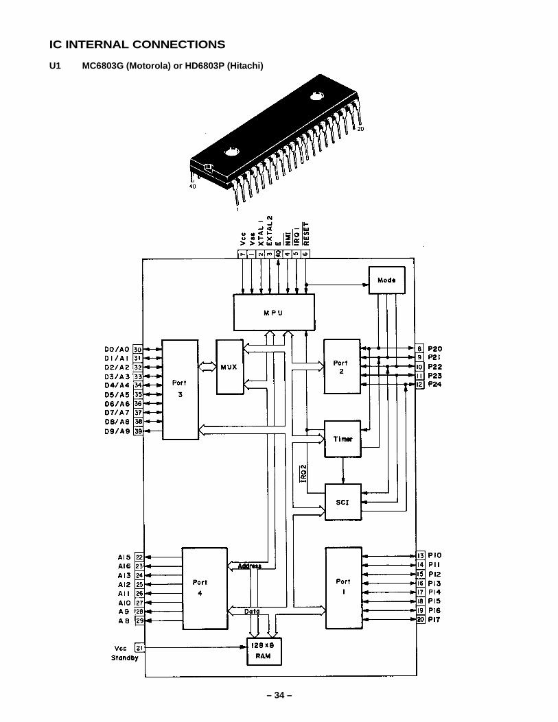
IC INTERNAL CONNECTIONS
U1 MC6803G (Motorola) or HD6803P (Hitachi)

– 35 –
U11 MC6847P (Motorola)

– 36 –
U2 SN74LS373N (Motorola) or MB74LS373M (Fujitsu)
U7 SN74LS245N (Motorola) or MB74LS245M (Fujitsu)

– 37 –
U3 MB8364M (Fujitsu)
U9/10 µPD4016C-1 (NEC) or µPD4016D-1 (NEC) or MB8128-15P (Fujitsu) or MSM2128-20RS (Oki)

– 38 –
U4 SN74LS155N (Motorola) or MB74LS155M (Fujitsu) or HD74LS155P (Hitachi)
U5/6 SN74LS367AN (Motorola) or MB74LS367AM (Fujitsu) or HD74LS367AP (Hitachi)

– 39 –
U8 SN74LS174N (Motorola) or MB74LS174M (Fujitsu) or HD74LS174P (Hitachi)
U14 MC14503BCP (Motorola) or HD14503BP (Hitachi) or µPD4503BC (NEC) or MSM4503RS (Oki)
U19 SN74LS76AN (Motorola) or MB74LS76AM (Fujitsu) or HD74LS76P (Hitachi)

– 40 –
U12 SN74LS14N (Motorola) or MB74LS14M (Fujitsu) or HD74LS14P (Hitachi)
U13 SN74LS32N (Motorola) or MB74LS32M (Fujitsu) or HD74LS32P (Hitachi)
U20 SN74LS32N (Motorola) or MB74LS32M (Fujitsu) or HD74LS32P (Hitachi)

– 41 –
U15 LM339N (Motorola) or µPC339C (NEC)
U18 SN74LS74AN (Motorola) or MB74LS74AM (Fujitsu) or HD74LS74AP (Hitachi)
– 42 –
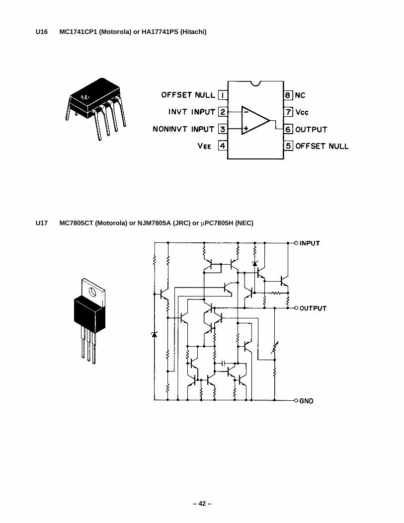
U16 MC1741CP1 (Motorola) or HA17741PS (Hitachi)
U17 MC7805CT (Motorola) or NJM7805A (JRC) or µPC7805H (NEC)
– 43 –
SECTION IX
SCHEMATlC DlAGRAM
SECTION X
EXPLODED VlEW

RADIO SHACK, A DIVISION OF TANDY CORPORATION
U.S.A.: FORT WORTH, TEXAS 76102CANADA: BARRIE. ONTARIO L4M 4W5
TANDY CORPORATION
6A3 Printed in U.S.A.
AUSTRALIA BELGIUM U. K.
91 KURRAJONG ROAD PARC INDUSTRIEL DE NANINNE BILSTON ROAD WEONESBURY
MOUNT ORUITT, N.S.W. 2770 5140 NANINNE WEST MIDLANDS WS10 7JN