256-tap non-volatile digital potentiometer sheets/winbond pdfs... · 256-tap non-volatile digital...
TRANSCRIPT

PRELIMINARY
Publication Release Date: April 22, 2005 - 1 - Revision 1.2
WMS7201
256-TAP NON-VOLATILE DIGITAL POTENTIOMETER
WMS7201
- 2 -
1. GENERAL DESCRIPTION The WMS7201 is a 256-tap, single-channel non-volatile digital potentiometer available in 10KΩ, 50KΩ and 100KΩ end-to-end resistances. These devices can be used as a three-terminal potentiometer or as a two terminal variable resistor in a wide variety of applications. The output of the potentiometer is determined by the wiper position, which varies linearly between VA and VB terminal according to the content stored in the volatile Tap Register (TR). The settings of the TR can be provided either directly by the user through the industry standard SPI interface, or by the non-volatile memory (NVMEM0~3) where the previous settings are stored. When changes are made to the TR to establish a new wiper position, the value of the setting can be saved into any non-volatile memory location (NVMEM0~3) by executing a NVMEM save operation. Upon powerup the content of the NVMEM0 is automatically loaded to the Tap Register. The WMS7201 contains a single potentiometer in 8-pin PDIP, SOIC, MSOP or 10 pin TSSOP packages and can operate over a wide operating voltage range from 2.7V to 5.5V. A selectable output buffer is built-in for those applications where an output buffer is required.
2. FEATURES • 256 taps for the potentiometer
• End-to-end resistance available in 10KΩ, 50KΩ and 100KΩ • Selectable output buffer for each channel • SPI Serial Interface for data transfer and potentiometer control • Daisy-chain operation for multiple devices (10-pin TSSOP package only) • Nonvolatile storage of four wiper positions per channel with power-on recall from NVMEM0
• Low standby current (1μA Max. with output buffer inactive) • Endurance 100K typical stores per bit • Register Data Retention 100 years
• Industrial temperature range: -40 ~ 85°C • Wide operating voltage range: 2.7V ~ 5.5V • Package option:
8-pin MSOP, 8-pin SOIC, 8-pin PDIP, 10-pin TSSOP

WMS7201
Publication Release Date: April 22, 2005 - 3 - Revision 1.2
3. BLOCK DIAGRAM
Serial
Interface Ta
p R
egis
ter
Dec
oder
MU
X
Power on/Preset Mem Tap
3 Addressable Preset Tap values
NV Memory9 th bit
9 th bit
CS SDI
CLK
V
SD O 1
DD
WP
1
NV Memory Control VSS
VA
1VW
VB1
1
FIGURE 1 – WMS7201 BLOCK DIAGRAM
Note 1: Available in 10-pin TSSOP packages only.

WMS7201
- 4 -
4. TABLE OF CONTENTS 1. GENERAL DESCRIPTION.................................................................................................................. 2 2. FEATURES ......................................................................................................................................... 2 3. BLOCK DIAGRAM .............................................................................................................................. 3 4. TABLE OF CONTENTS ...................................................................................................................... 4 5. PIN CONFIGURATION ....................................................................................................................... 5 6. PIN DESCRIPTION............................................................................................................................. 5 7. FUNCTIONAL DESCRIPTION............................................................................................................ 7
7.1. Potentiometer and Rheostat Modes ............................................................................................. 7 7.1.1. Rheostat Configuration .......................................................................................................... 7 7.1.2. Potentiometer Configuration .................................................................................................. 7
7.2. Programming Modes .................................................................................................................... 7 7.3. Non-Volatile Memory (NVMEM) ................................................................................................... 8
7.3.1 Write Protect of NVMEM......................................................................................................... 8 7.4 Flow Control................................................................................................................................... 8 7.5. Daisy Chain .................................................................................................................................. 9 7.6. Serial Data Iterface ..................................................................................................................... 10 7.7. Instruction Set............................................................................................................................. 12 7.8. Basic Operation .......................................................................................................................... 12
7.8.1 Sending a Command ............................................................................................................ 12 7.8.2 Wake Up/Sleep/Power Commands ...................................................................................... 13 7.8.3 Write to Tap Register (TR).................................................................................................... 13 7.8.4 Programming Non-Volatile Memory (NVMEM)..................................................................... 14 7.8.5 Reading Tap Register and NVMEM Location (10-pin TSSOP package only)...................... 15
8. TIMING DIAGRAMS.......................................................................................................................... 16 9. ABSOLUTE MAXIMUM RATINGS.................................................................................................... 18 10. ELECTRICAL CHARACTERISTICS ............................................................................................... 19
10.1 Test Circuits ............................................................................................................................... 21 11. TYPICAL APPLICATION CIRCUIT................................................................................................. 22
11.1. Layout Considerations .............................................................................................................. 24 12. PACKAGE DRAWINGS AND DEMINSIONS.................................................................................. 25 13. ORDERING INFORMATION........................................................................................................... 28 14. VERSION HISTORY ....................................................................................................................... 29

WMS7201
Publication Release Date: April 22, 2005 - 5 - Revision 1.2
5. PIN CONFIGURATION
FIGURE 2 – PACKAGE TYPES
WMS7201
- 6 -
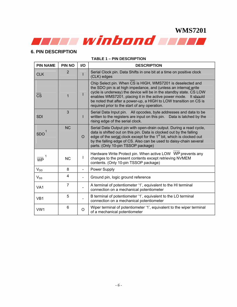
6. PIN DESCRIPTION TABLE 1 – PIN DESCRIPTION
PIN NAME PIN NO I/O DESCRIPTION
CLK 2 I Serial Clock pin. Data Shifts in one bit at a time on positive clock (CLK) edges
CS 1 I
Chip Select pin. When CS is HIGH, WMS7201 is deselected and the SDO pin is at high impedance, and (unless an internal write cycle is underway) the device will be in the standby state. CS LOW enables WMS7201, placing it in the active power mode. It should be noted that after a power-up, a HIGH to LOW transition on CS is required prior to the start of any operation.
SDI 3
I Serial Data Input pin. All opcodes, byte addresses and data to be written to the registers are input on this pin. Data is latched by the rising edge of the serial clock.
SDO
NC
O
Serial Data Output pin with open-drain output. During a read cycle, data is shifted out on this pin. Data is clocked out by the falling edge of the serial clock except for the 1st bit, which is clocked out by the falling edge of CS. Also can be used to daisy-chain several parts. (Only 10-pin TSSOP package)
1
WP
NC I
Hardware Write Protect pin. When active LOW WP prevents any changes to the present contents except retrieving NVMEM contents. (Only 10-pin TSSOP package)
1
VDD 8 - Power Supply
VSS4 - Ground pin, logic ground reference
VA1 7 - A terminal of potentiometer ‘1’, equivalent to the HI terminal connection on a mechanical potentiometer
VB1 5 - B terminal of potentiometer ‘1’, equivalent to the LO terminal connection on a mechanical potentiometer
6 Wiper terminal of potentiometer ‘1’, equivalent to the wiper terminal of a mechanical potentiometer VW1 O
WMS7201
Publication Release Date: April 22, 2005 - 7 - Revision 1.2
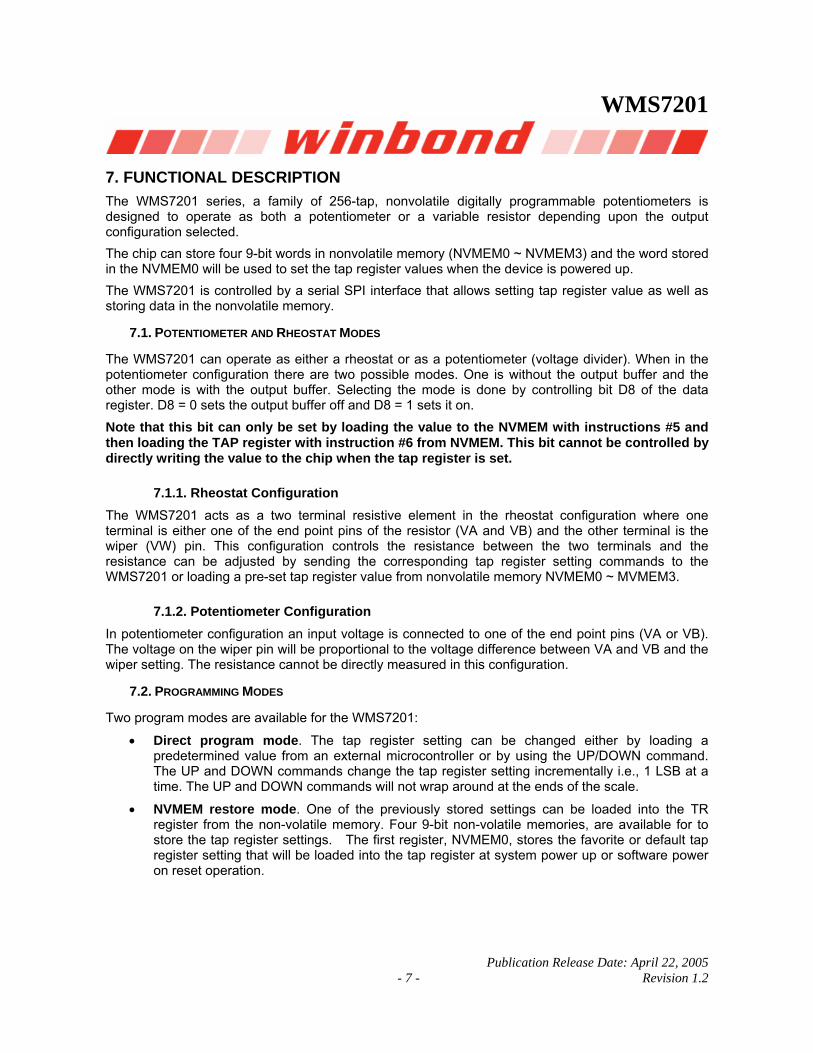
7. FUNCTIONAL DESCRIPTION The WMS7201 series, a family of 256-tap, nonvolatile digitally programmable potentiometers is designed to operate as both a potentiometer or a variable resistor depending upon the output configuration selected. The chip can store four 9-bit words in nonvolatile memory (NVMEM0 ~ NVMEM3) and the word stored in the NVMEM0 will be used to set the tap register values when the device is powered up. The WMS7201 is controlled by a serial SPI interface that allows setting tap register value as well as storing data in the nonvolatile memory.
7.1. POTENTIOMETER AND RHEOSTAT MODES
The WMS7201 can operate as either a rheostat or as a potentiometer (voltage divider). When in the potentiometer configuration there are two possible modes. One is without the output buffer and the other mode is with the output buffer. Selecting the mode is done by controlling bit D8 of the data register. D8 = 0 sets the output buffer off and D8 = 1 sets it on. Note that this bit can only be set by loading the value to the NVMEM with instructions #5 and then loading the TAP register with instruction #6 from NVMEM. This bit cannot be controlled by directly writing the value to the chip when the tap register is set.
7.1.1. Rheostat Configuration The WMS7201 acts as a two terminal resistive element in the rheostat configuration where one terminal is either one of the end point pins of the resistor (VA and VB) and the other terminal is the wiper (VW) pin. This configuration controls the resistance between the two terminals and the resistance can be adjusted by sending the corresponding tap register setting commands to the WMS7201 or loading a pre-set tap register value from nonvolatile memory NVMEM0 ~ MVMEM3.
7.1.2. Potentiometer Configuration In potentiometer configuration an input voltage is connected to one of the end point pins (VA or VB). The voltage on the wiper pin will be proportional to the voltage difference between VA and VB and the wiper setting. The resistance cannot be directly measured in this configuration.
7.2. PROGRAMMING MODES
Two program modes are available for the WMS7201:
• Direct program mode. The tap register setting can be changed either by loading a predetermined value from an external microcontroller or by using the UP/DOWN command. The UP and DOWN commands change the tap register setting incrementally i.e., 1 LSB at a time. The UP and DOWN commands will not wrap around at the ends of the scale.
• NVMEM restore mode. One of the previously stored settings can be loaded into the TR register from the non-volatile memory. Four 9-bit non-volatile memories, are available for to store the tap register settings. The first register, NVMEM0, stores the favorite or default tap register setting that will be loaded into the tap register at system power up or software power on reset operation.

WMS7201
- 8 -
7.3. NON-VOLATILE MEMORY (NVMEM)
The WMS7201 has four NVMEM positions available for storing the output buffer operating mode and the potentiometer setting. These NVMEM positions can be directly written through the SPI using a write command (#5) with address and data bytes. Another command (#7) is available that stores the current output buffer operating mode and potentiometer settings into the selected NVMEM position. Bit A3 and A2 in the instruction byte decide which NVMEM position is used. (See Table 5) The potentiometer is loaded with the value stored in the NVMEM position 0 on power up.
7.3.1 Write Protect of NVMEM
Write-Protect ( WP ) disables any changes of current content in the NVMEM regardless of the commands, except that NVMEM setting can be retrieved using commands 4, 6 of Table 5. Therefore, Write-Protect ( WP ) pin provides hardware NVMEM protection feature with WP tied to Vss. WP , which is active at logic LOW, should be tied directly to VDD if it is not being used. This function is only available on the 10-pin package.
7.4 FLOW CONTROL
Reading and writing to NVMEM requires an internal access cycle to complete before the next command can be sent. Read Tap Register (#2) Read NVMEM (#4) Program NVMEM (#5) Load Tap Register(#6) Program NVMEM with Tap Register (#7)
WMS7201
Publication Release Date: April 22, 2005 - 9 - Revision 1.2
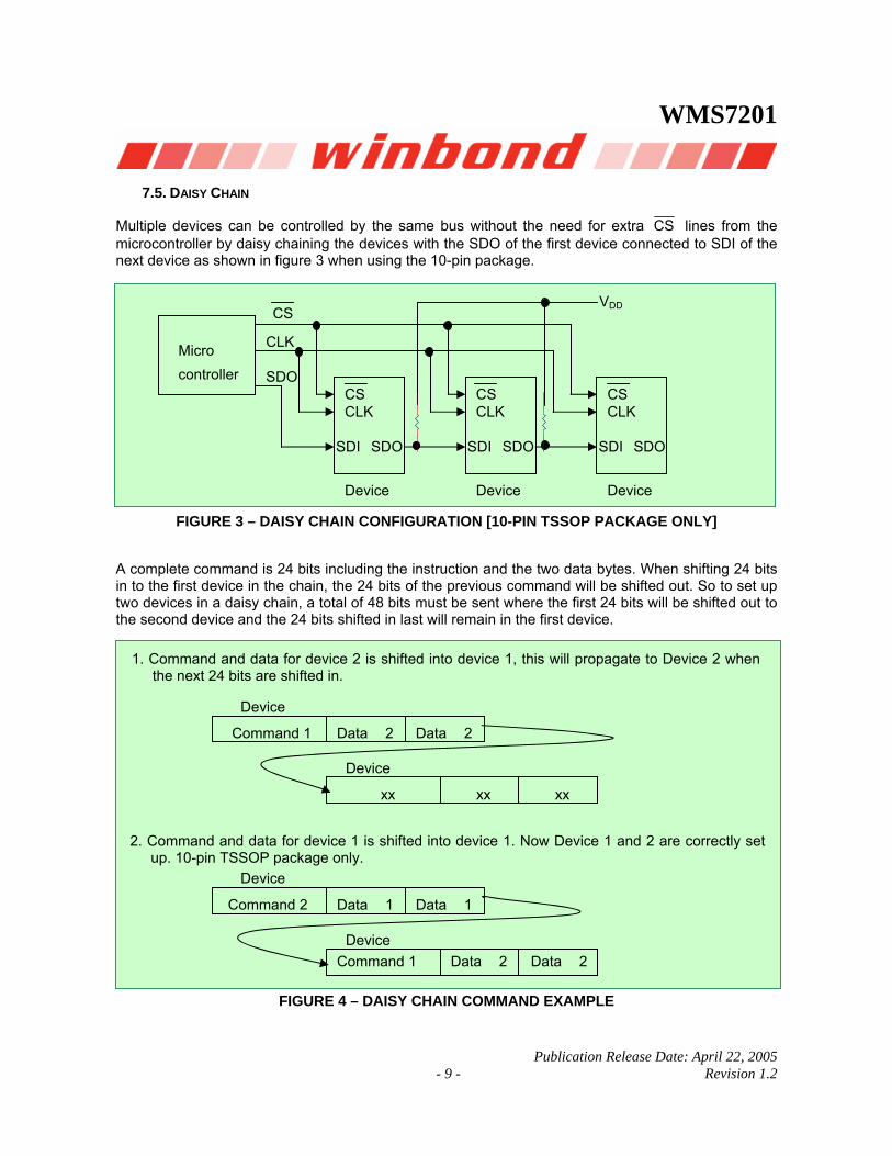
7.5. DAISY CHAIN
Multiple devices can be controlled by the same bus without the need for extra CS lines from the microcontroller by daisy chaining the devices with the SDO of the first device connected to SDI of the next device as shown in figure 3 when using the 10-pin package.
controller Micro
Device Device Device
CS
CLK
SDO
SDI SDO SDI SDO SDI SDO
CS CSCLK CLK CLK
CS
VDD
FIGURE 3 – DAISY CHAIN CONFIGURATION [10-PIN TSSOP PACKAGE ONLY] A complete command is 24 bits including the instruction and the two data bytes. When shifting 24 bits in to the first device in the chain, the 24 bits of the previous command will be shifted out. So to set up two devices in a daisy chain, a total of 48 bits must be sent where the first 24 bits will be shifted out to the second device and the 24 bits shifted in last will remain in the first device.
1. Command and data for device 2 is shifted into device 1, this will propagate to Device 2 when the next 24 bits are shifted in.
Command 1 Data 2 Data 2
xx xx xx
Device
Device
Device
Command 2 Data 1 Data 1
Command 1 Data 2 Data 2 Device
2. Command and data for device 1 is shifted into device 1. Now Device 1 and 2 are correctly set up. 10-pin TSSOP package only.
FIGURE 4 – DAISY CHAIN COMMAND EXAMPLE

WMS7201
- 10 -
7.6. SERIAL DATA ITERFACE
The WMS7201 contains a four-wire SPI interface:
• SDO (Serial Data Output) Used for reading out the internal register contents and for daisy chaining multiple devices on the 10-pin package.
• SDI (Serial Data Input) Used for clocking in commands and potentiometer settings.
• CS (Chip Select) This pin must be pulled LOW before starting to send a command and pulled HIGH to signal the end of the command; this pin can be used to control multiple devices on the bus.
• CLK (Clock) The SDI bits are shifted in on the rising edge of the clock and SDO data is shifted out on the falling edge of the clock.
The key features of this interface include:
• Independently programmable Read & Write to all registers
• Direct parallel refresh of Tap register from corresponding internal NVMEM registers
• Increment and decrement instruction for Tap register
• Nonvolatile storage of the present Tap register values into one of the four NVMEM registers available.
• Configurable output buffer amplifier to allow both the functions of a potentiometer and a variable resistor
• Four 9-bit non-volatile registers store four preset wiper positions and the first one will be recalled to set the wiper position during power up.
The serial interface uses an SPI compatible uniform 24-bit word format as shown below. This format is used for all members of the WMS720x family. The data is sent MSB first.
TABLE 2 – 24-BIT DATA WORD FORMAT
MSB LSB
C3 C2 C1 C0 A3 A2 A1 A0 X X X X X X X D8 D7 D6 D5 D4 D3 D2 D1 D0
C3-C0 are the command bits that control the operation of the digital potentiometer according to the command instructions shown in the Instruction Set in Table 5 in Section 7.7. A1 and A0 are the address bits that determine which channel is activated in the WMS720x family as shown in the table below. For the WMS7201 A0 and A1 are always set to 0.
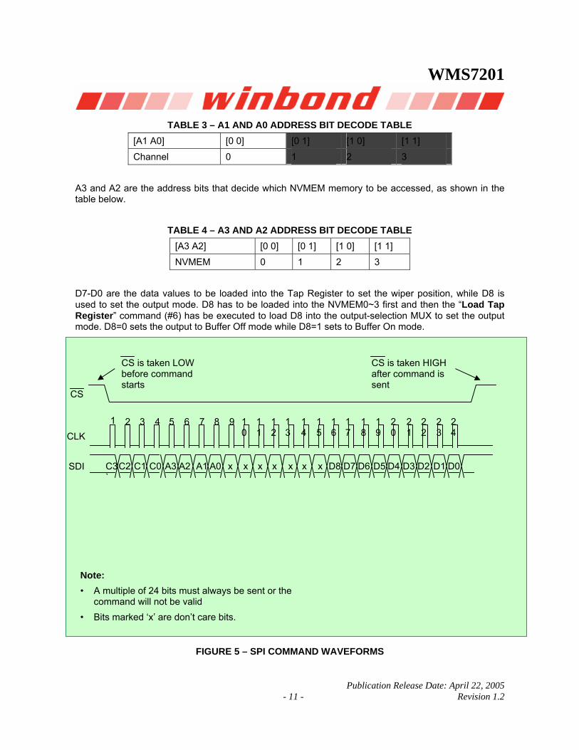
WMS7201
Publication Release Date: April 22, 2005 - 11 - Revision 1.2
TABLE 3 – A1 AND A0 ADDRESS BIT DECODE TABLE [A1 A0] [0 0] [0 1] [1 0] [1 1]
Channel 0 1 2 3
A3 and A2 are the address bits that decide which NVMEM memory to be accessed, as shown in the table below.
TABLE 4 – A3 AND A2 ADDRESS BIT DECODE TABLE [A3 A2] [0 0] [0 1] [1 0] [1 1]
NVMEM 0 1 2 3
D7-D0 are the data values to be loaded into the Tap Register to set the wiper position, while D8 is used to set the output mode. D8 has to be loaded into the NVMEM0~3 first and then the “Load Tap Register” command (#6) has be executed to load D8 into the output-selection MUX to set the output mode. D8=0 sets the output to Buffer Off mode while D8=1 sets to Buffer On mode.
FIGURE 5 – SPI COMMAND WAVEFORMS
C3`
C2 C1 C0 A3 A2 A1 A0 x x x x x x x D8 D7 D6 D5 D4 D3 D2 D1 D0
1 2 3 4 5 6 7 8 9 10
11
12
13
14
15
16
17
18
19
20
21
22
23
24 CLK
SDI
• Bits marked ‘x’ are don’t care bits.
• A multiple of 24 bits must always be sent or the command will not be valid
Note:
CS
CS is taken LOW before command starts
CS is taken HIGH after command is sent

WMS7201
- 12 -
7.7. INSTRUCTION SET
TABLE 5 – INSTRUCTION SET Inst No.
Instruction Byte
C3 C2 C1 C0 A3 A2 A1 A0
Data Byte 1
D15 D14 D13 D12 D11 D10 D9 D8
Data Byte 2
D7 D6 D5 D4 D3 D2 D1 D0
Operation
1 0 0 0 0 x x x x x x x x x x x x x x x x x x x x No Operation (NOP). Do nothing
2 1 1 0 0 x x A1 A0 x x x x x x x x x x x x x x x x Read Tap Register and output selection MUX register
3 0 1 0 0 x x A1 A0 x x x x x x x x D7 D6 D5 D4 D3 D2 D1 D0 Write to Tap Register with D7-D0
4 1 0 1 0 A3 A2 A1 A0 x x x x x x x x x x x x x x x x Read NVMEM pointed to by A3-A0
5 0 0 1 0 A3 A2 A1 A0 x x x x x x x D8
D7 D6 D5 D4 D3 D2 D1 D0 Program NVMEM pointed to by A3-A0 with D8-D0
6 1 0 1 1 A3 A2 A1 A0 x x x x x x x x x x x x x x x x Load Tap Register and output selection MUX register with the contents of NVMEM pointed to by A3-A0
7 0 0 1 1 A3 A2 A1 A0 x x x x x x x x x x x x x x x x Program NVMEM pointed to by A3-A0 with the contents of Tap Register and output selection MUX register
8 0 1 1 1 x x A1 A0 x x x x x x x x x x x x x x x x Up: Increment setting of TR by one tap
9 1 1 1 1 x x A1 A0 x x x x x x x x x x x x x x x x Down: Decrement setting of TR by one tap
10 1 0 0 0 x x x x x x x x x x x x x x x x x x x x Sleep: Discontinue clock supply to the logic and memories
11 0 0 0 1 x x x x x x x x x x x x x x x x x x x x Wake Up: Clock supply to the logic and memories
12 1 1 0 1 A3 A2 A1 A0 x x x x x x x x x x x x x x x x Byte-erase NVMEM pointed to by A3-A0
13 1 0 0 1 x x x x x x x x x x x x x x x x x x x x Power On Reset: Software reset the part to the power up state
Note: C3-C0 are the command op-code; A3, A2 are the NVMEM address; A1, A0 are the channel address.
7.8. BASIC OPERATION
This chapter describes the sequences of commands to send to the WMS7201 and how to use the different features.
7.8.1 Sending a Command 1. Take the chip out of SLEEP mode. 2. Check that the write protect is set correctly if writing to NVMEM (10-pin TSSOP package
only).
3. Pull the CS pin LOW before sending data to the device.
WMS7201
Publication Release Date: April 22, 2005 - 13 - Revision 1.2
4. 24 clock pulses are sent for each command. SDI must be valid on the rising edge of the clock, SDO is valid on the falling edge of the clock or CS .
5. Take CS HIGH after the command has completed
6. If command 2, 4, 5, 6 or 7 is sent, wait TSV time before sending the next command.
7.8.2 Wake Up/Sleep/Power Commands The chip is in SLEEP mode after:
• VDD is applied
• A Power on Reset command is sent
• A SLEEP command is sent Before any operations can be performed the WAKE UP command must be sent. When a SLEEP command is sent, the chip retains its resistor settings as long as the chip is powered up but cannot accept any other commands than a WAKE UP command.
TABLE 6 – POWER RELATED COMMANDS Inst. No.
Command Name:
Command Byte Data Byte 1 Data Byte 2 Comment
11 Wake Up 0 0 0 1 x x x x x x x x x x x x x x x x x x x x Wake Up entire chip
10 Sleep 1 0 0 0 x x x x x x x x x x x x x x x x x x x x Send chip into power save mode
13 Power on Reset 1 0 0 1 x x x x x x x x x x x x x x x x x x x x Reset Chip
1 NOP 0 0 0 0 x x x x x x x x x x x x x x x x x x x x Dummy instruction
The commands above control the entire chip.
7.8.3 Write to Tap Register (TR) The microcontroller can write a value directly into the tap register or send an increment or decrement command to control the tap register. Alternatively, the contents of an NVMEM location can be written to the tap register. The only way to change the output buffer mode is to write the desired value of bit D8 into an NVMEM location and then load the corresponding NVMEM location into the tap register.

WMS7201
- 14 -
TABLE 7 – WRITING TO THE TAP REGISTERS Inst. No.
Command Name:
Command Byte Data Byte 1 Data Byte 2 Comment
3 Write to Tap Register
0 1 0 0 x x 0 0 x x x x x x x x D7 D6 D5 D4 D3 D2 D1 D0 Writes a value to the tap register.
8 Up 0 1 1 1 x x 0 0 x x x x x x x x x x x x x x x x Increment tap register value by one
9 Down 1 1 1 1 x x 0 0 x x x x x x x x x x x x x x x x Decrement tap register value by one
6 Load Tap Register
1 0 1 1 A3 A2 0 0 x x x x x x x x x x x x x x x x Load the selected NVMEM location into the tap register
7.8.4 Programming Non-Volatile Memory (NVMEM) The value stored in the NVMEM location is 9 bits, the 8 bits (D7-D0) of the tap register plus 1 bit (D8) of the output buffer mode. The NVMEM position must be erased before writing to it. There are two ways to program a value into NVMEM. Write a value directly from the microcontroller. Load the current potentiometer setting into NVMEM.
TABLE 8 – PROGRAMMING NVMEM Inst. No
Command Name
Command Byte Data Byte 1 Data Byte 2 Comment
12 Erase NVMEM
1 1 0 1 A3 A2 0 0 x x x x x x x x x x x x x x x x Erases the 9 bit word pointed to by A3, A2, A1 and A0.
5 Program NVMEM
0 0 1 0 A3 A2 0 0 x x x x x x x D8 D7 D6 D5 D4 D3 D2 D1 D0 Writes a value to the NVMEM register.
7 Program NVMEM with Tap Register
0 0 1 1 A3 A2 0 0 x x x x x x x x x x x x x x x x Takes the current potentiometer settings and saves in the selected NVMEM location.
For programming NVMEM, the following sequence must be followed:
1. Erase word at NVMEM location 2. Program word at NVMEM location

WMS7201
Publication Release Date: April 22, 2005 - 15 - Revision 1.2
7.8.5 Reading Tap Register and NVMEM Location (10-pin TSSOP package only) The contents of the tap register or any NVMEM location can be read back through the SDO pin. When a command is sent, the data is clocked out on the falling edge of the clock. Since daisy-chain operation requires data from one command to be clocked out when the next command arrives, any read command must be followed by another command to get the correct data on the SDO pin.
TABLE 9 – READING THE TAP REGISTER Inst. No.
Command Name:
Command Byte Data Byte 1 Data Byte 2 Comment
4 Read NVMEM
1 0 1 0 A3 A2 0 0 x x x x x x x x x x x x x x x x Read the value of the selected NVMEM location
2 Read Tap Register
1 1 0 0 x x 0 0 x x x x x x x x x x x x x x x x Read the value of the selected tap register
1 NOP to Read Register
0 0 0 0 x x x x x x x x x x x D8 D7 D6 D5 D4 D3 D2 D1 D0 Output data to SDO pin
To read the contents of either the tap register or a NVMEM location, the following sequence must be followed.
1. Send the desired read command (#2 or #4) 2. Send another command such as NOP and read the SDO pin on the falling edge of the clock.
The other command could be any command, but to make sure that the chip does not change anything, send either another Read command or a NOP command (#1).

WMS7201
- 16 -
8. TIMING DIAGRAMS
FIGURE 6 – WMS7201 TIMING DIAGRAM Notes: (1) Internal signal only. (2) Only on 10-pin TSSOP package.
tLEAD
tCYC tWL tWH
tLAG
tCS tDH tDSU
tLAC tPD tLRL
tRSU tST
tSV
CLK
CS
MSB LSBSDI
SDO
R/B tWPSU tWPH
MSB LSB
1
2 WP

WMS7201
Publication Release Date: April 22, 2005 - 17 - Revision 1.2
TABLE 10 – TIMING PARAMETERS
PARAMETER SYMBOL MIN. MAX. UNIT SPI Clock Cycle Time tCYC 100 ns
SPI Clock HIGH Time tWH 50 ns
SPI Clock LOW Time tWL 50 ns
Lead Time tLEAD 100 ns
Lag Time tLAG 100 ns
SDI Setup Time tDSU 20 ns
SDI Hold Time tDH 20 ns
CS to SDO – SPI Line Acquire 1 tLAC 5 ns
CS to SDO – SPI Line Release 1 tLRL 5 ns
CLK to SDO Propagation Delay 1 tPD 1 ns
Store to NVMEM Save Time tSV 2 ms
CS Deselect Time tCS 600 ns
Startup Time tST 0.1 ms
WP Setup Time 1 tWPSU 10 ns
tWPH 10 WP Hold Time 1 ns
Note: The interface timing characteristics apply to all parts but are guaranteed by design and not subject to production test. Note 1: 10-pin package only.

WMS7201
- 18 -
9. ABSOLUTE MAXIMUM RATINGS TABLE 11 – ABSOLUTE MAXIMUM RATINGS
Condition Value Junction temperature 150ºC
Storage temperature -65º to +150ºC
Voltage applied to any pad (Vss – 0.3V) to (VDD + 0.3V)
VDD – VSS -0.3 to 7.0V
Note: Exposure to conditions beyond those listed under: Absolute Maximum Ratings, may adversely affect the life and reliability of the device.
WMS7201
Publication Release Date: April 22, 2005 - 19 - Revision 1.2
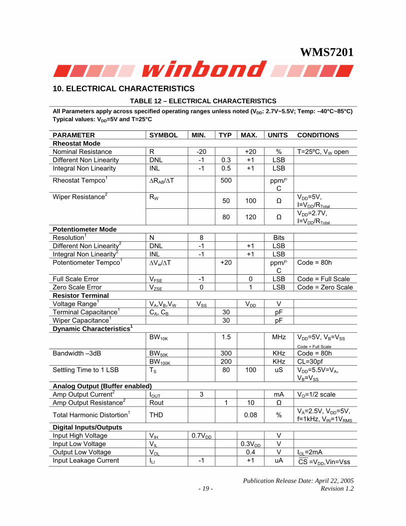
10. ELECTRICAL CHARACTERISTICS TABLE 12 – ELECTRICAL CHARACTERISTICS
All Parameters apply across specified operating ranges unless noted (VDD: 2.7V~5.5V; Temp: –40°C~85°C) Typical values: VDD=5V and T=25°C PARAMETER SYMBOL MIN. TYP MAX. UNITS CONDITIONS Rheostat Mode Nominal Resistance R -20 +20 % T=25ºC, VW open Different Non Linearity DNL -1 0.3 +1 LSB Integral Non Linearity INL -1 0.5 +1 LSB
Rheostat Tempco1 ΔRAB/ΔT 500 ppm/°C
Wiper Resistance2 RW 50 100 Ω VDD=5V, I=VDD/RTotal
80 120 Ω VDD=2.7V, I=VDD/RTotal
Potentiometer Mode Resolution1 N 8 Bits Different Non Linearity2 DNL -1 +1 LSB Integral Non Linearity2 INL -1 +1 LSB Potentiometer Tempco1 ΔVw/ΔT +20 ppm/°
C Code = 80h
Full Scale Error VFSE -1 0 LSB Code = Full Scale Zero Scale Error VZSE 0 1 LSB Code = Zero ScaleResistor Terminal Voltage Range1 VA,VB,VB W VSS VDD V Terminal Capacitance1 CA, CBB 30 pF Wiper Capacitance1 30 pF Dynamic Characteristics1 BW10K 1.5 MHz VDD=5V, VB=VB SS
Code = Full Scale
Bandwidth –3dB BW50K 300 KHz Code = 80h BW100K 200 KHz CL=30pf Settling Time to 1 LSB TS 80 100 uS VDD=5.5V=VA,
VB=VB SS
Analog Output (Buffer enabled) Amp Output Current2 IOUT 3 mA VO=1/2 scale Amp Output Resistance2 Rout 1 10 Ω
Total Harmonic Distortion1 THD 0.08 % VA=2.5V, VDD=5V, f=1kHz, VIN=1VRMS
Digital Inputs/Outputs Input High Voltage VIH 0.7VDD V Input Low Voltage VIL 0.3VDD V Output Low Voltage VOL 0.4 V IOL=2mA Input Leakage Current ILI -1 +1 uA CS =VDD,Vin=Vss

WMS7201
- 20 -
~ VDD
Output Leakage Current ILo -1 +1 uA CS =VDD,Vin=VSS ~ VDD
Input Capacitance1 CIN 25 pF VDD=5V, fc = 1Mhz Code = 80h
Output Capacitance1 COUT 25 pF VDD=5V, fc = 1MhzCode = 80h
Power Requirements Operating Voltage1 VDD 2.7 5.5 V
Operating Current IDDR 1 1.8 mA All ops except NVMEM program
Operating Current 1 2 mA During Non-volatile memory program
IDDW
ISA 0.5 1 mA Buffer is active, , no load
Standby Current ISB
2 0.1 1 uA Buffer is inactive, Power Down, No load
Power Supply Rejection Ratio VDD=5V±10%, Code=80h PSRR 1 LSB/V
Note: 1. Not subject to production test; 2. Only on Final Test; 3. VDD = +2.7V to 5.5V, VSS = 0V, T = 25ºC, unless otherwise noted.

WMS7201
Publication Release Date: April 22, 2005 - 21 - Revision 1.2
10.1 TEST CIRCUITS
FIGURE 7 – TEST CIRCUITS
Potentiometer divider nonlinearity error test circuit (INL, DNL)
*Assume infinite input impedance
V +
VMS*
V+ = VDD 1LSB= V+/255
WMS7201
VA
VB B
VW
Resistor position nonlinearity error test circuit (Rheostat Operation: R-INL, R-DNL)
*Assume infinite input impedance
No Connection
V MS *
WMS7201
WVA
VBB
VW
IW
WMS7201
10%
Wiper resistance test circuit
*Assume infinite input impedance
V MS*
WMS7201
VA
VBB
VW
IW I W = V DD /R Total
R W = V MS /I W
Power supply sensitivity test circuit (PSS, PSRR)
*Assume infinite input impedance
V+
V+ = V DD ±
VA
VBB
VW
VMS*
PSRR(dB) = 20LOG ( Δ VΔ
) MS VDD
PSS(%/% ) = VΔ M VΔ S
DD
WMS7201 VA VB B
VW
VIN~
+5V
V OUT
2.5V DCOffset
Capacitance test circuit
VA
VBB
WMS7201
VW VIN ~
+5V
OFFSETGND
VOUT
2.5V DC
Gain vs. frequency test circuit

WMS7201
- 22 -
11. TYPICAL APPLICATION CIRCUIT
Vin
VOUT = - VIN A
B
RR
RA = 256
D)(256RAB − , RB = B
256DRAB
RAB = Total resistance of potentiometer D = Wiper setting for WMS7201
FIGURE 8 – PROGRAMMABLE INVERTING GAIN AMPLIFIER USING THE WMS7201
VOUT = VIN (1+A
B
RR
)
RA = 256
D)(256RAB − , RB = B
256DRAB
RAB = Total resistance of potentiometer D = Wiper setting for WMS7201
FIGURE 9 – PROGRAMMABLE NON-INVERTING GAIN AMPLIFIER USING THE WMS7201
OP AMP
_ VOUT
WMS7201
+
OP AMP
VIN VOUT
WMS7201
_
RA RB
+
RA RB B

WMS7201
Publication Release Date: April 22, 2005 - 23 - Revision 1.2
VREF = 5.0v
GND
VREFH
WMS7201
V+
I = 32mA
FIGURE 10 – WMS7201 TRIMMING VOLTAGE REFERENCE
SDI CS\
RF Input
FILTER
L1 CHOKE
WMS7201 WINPOT
1 2 3 4
765
8CSCLKSDIVSS
VA1VW1VB1
VDD RF OUT
VDD
Q1
RF POWER AMP
C10.1uF
C2
CLK
FIGURE 11 – WMS7201 RF AMP CONTROL

WMS7201
- 24 -
11.1. LAYOUT CONSIDERATIONS
A 0.1μF bypass capacitor as close as possible to the VDD pin is recommended for best performance. Often this can be done by placing the surface mount capacitor on the bottom side of the PC board, directly between the VDD and VSS pins. Care should be taken to separate the analog and digital traces. Sensitive traces should not run under the device or close to the bypass capacitors. A dedicated plane for analog ground helps in reducing ground noise for sensitive analog signals.
FIGURE 12 – WMS7201 LAYOUT

WMS7201
Publication Release Date: April 22, 2005 - 25 - Revision 1.2
12. PACKAGE DRAWINGS AND DEMINSIONS
L
O
c
D
A1
A
e
bSEATING PLANE
Y
0.25
GAUGE PLANE
E HE
1
8 5
4
4.00
0.25
0.510.25
E
cbA1
3.80
0.190.330.10
0.1570.010
0.0200.010
0.1500.008
0.0130.004
MAX.DIMENSION IN MM
1.75A
SYMBOLMIN.1.35
DIMENSION IN INCH
0.069MIN.
0.053MAX.
Control demensions are in milmeters .
1.270.106.20
L
θ
YH
0 100.40
5.80
e 1.27 BSC
0.050
0.0040.244
00.016
0.228
10
0.050 BSC
E
D 4.80 5.00 0.188 0.196
FIGURE 13 – 8L SOIC – 150MIL

WMS7201
- 26 -
1E
D
1B
B
1.631.470.0640.058
SymbolMin Nom Max MaxNomMin
Dimension in inch Dimension in mm
A
B
cD
e
A
L
S
AA
1
2
E
0.060 1.52
0.175 4.45
0.010
0.125
0.016
0.130
0.018
0.135
0.022
3.18
0.41
0.25
3.30
0.46
3.43
0.56
0.008
0.120
0.375
0.010
0.130
0.014
0.140
0.20
3.05
0.25
3.30
0.36
3.56
0.2550.2500.245 6.486.356.22
9.53
7.627.37 7.870.3000.290 0.310
2.29 2.54 2.790.090 0.100 0.110
B 1
1
e
E 1
0.360 0.380 9.14 9.65
0 15
0.045 1.14
0.3550.335 8.51 9.02
150
Seating Plane
e A
2A
c
E
Base Plane1A
1e
L
A
S
8 5
1 4
α
α
FIGURE 14 – 8L PDIP

WMS7201
Publication Release Date: April 22, 2005 - 27 - Revision 1.2
FIGURE 15 – 8L MSOP

WMS7201
- 28 -
13. ORDERING INFORMATION Winbond’s WinPot Part Number Description:
WMS72 XX XXX X Winbond WinPot Products
Features:
• 01: Single channel with SPI Interface
• 02: Dual channels with SPI Interface
• 04: Quad channels with SPI Interface
End-to-end Resistance:
• 010: 10KΩ
• 050: 50KΩ
• 100: 100KΩ
• M: MSOP (Available only for single channel devices)
• P: PDIP
• S: SOIC
• T: TSSOP
Package Index:
For the latest product information, access Winbond’s worldwide website at http://www.winbond-usa.com

WMS7201
Publication Release Date: April 22, 2005 - 29 - Revision 1.2
14. VERSION HISTORY VERSION DATE DESCRIPTION
1.0 Jan. 2003 Initial issue
1.1 Jan. 2003 Correct typos
1.2 April. 2005
Revise disclaim section

WMS7201
- 30 -
The contents of this document are provided “AS IS”, and Winbond assumes no liability whatsoever and disclaims any express or implied warranty of merchantability, fitness for a particular purpose or infringement of any Intellectual property. In no event, shall Winbond be liable for any damages whatsoever (including, without limitation, damages for loss of profits, business interruption, loss of information) arising out of the use of or inability to use the contents of this documents, even if Winbond has been advised of the possibility of such damages.
Application examples and alternative uses of any integrated circuit contained in this publication are for illustration only and Winbond makes no representation or warranty that such applications shall be suitable for the use specified.
The 100-year retention and 100K record cycle projections are based upon accelerated reliability tests, as published in the Winbond Reliability Report, and are neither warranted nor guaranteed by Winbond. This product incorporates SuperFlash®.
This datasheet and any future addendum to this datasheet is(are) the complete and controlling ISD® ChipCorder® product specifications. In the event any inconsistencies exist between the information in this and other product documentation, or in the event that other product documentation contains information in addition to the information in this, the information contained herein supersedes and governs such other information in its entirety. This datasheet is subject to change without notice.
Copyright© 2005, Winbond Electronics Corporation. All rights reserved. ChipCorder® and ISD® are trademarks of Winbond Electronics Corporation. SuperFlash® is the trademark of Silicon Storage Technology, Inc. All other trademarks are properties of their respective owners.
Winbond products are not designed, intended, authorized or warranted for use as components in systems or equipment intended for surgical implantation, atomic energy control instruments, airplane or spaceship instruments, transportation instruments, traffic signal instruments, combustion control instruments, or for other applications intended to support or sustain life. Furthermore, Winbond products are not intended for applications wherein failure of Winbond products could result or lead to a situation wherein personal injury, death or severe property or environmental damage could occur.
Winbond customers using or selling these products for use in such applications do so at their own risk and agree to fully indemnify Winbond for any damages resulting from such improper use or sales.
The contents of this document are provided only as a guide for the applications of Winbond products. Winbond makes no representation or warranties with respect to the accuracy or completeness of the contents of this publication and reserves the right to discontinue or make changes to specifications and product descriptions at any time without notice. No license, whether express or implied, to any intellectual property or other right of Winbond or others is granted by this publication. Except as set forth in Winbond's Standard Terms and Conditions of Sale, Winbond assumes no liability whatsoever and disclaims any express or implied warranty of merchantability, fitness for a particular purpose or infringement of any Intellectual property.