2.4qvga spec a qvga tft lcm...(8) install the lcd module by using the mounting holes. when mounting...
TRANSCRIPT

© Haier Equipment Product Group
Product Specification 2.4″(240RGB*320)TFT-LCM
Revision: A
Customer Name:
Approved by:
Qingdao Haier Intelligent ElectrnicsCo. Ltd.
Prepared by: Pan Xinli Product Part No.: 2.4QVGA
Checked by: Qi Sen Product ID:
Approved by: Wen Guiqin Date: 2014.09.22
Address: Haier (Qingdao) Industry Zone, Haier Road No.1, Laoshan District, Qingdao, P.R.C.
Tel: 86-532-88937051 Fax: 86-532-88935273

Template ID: PDP03-050
Revision: V1.0 Product Specification
Released: 20101230
© Haier Equipment Product Group 第 2 页 共 23 页
Document History:
Mark Update Author Before Change After Change
2014-09-22 PanXinli /
First Release
Ver:A

Template ID: PDP03-050
Revision: V1.0 Product Specification
Released: 20101230
© Haier Equipment Product Group 第 3 页 共 23 页
Contents
1、 GENERAL INFORMATION ..................................................................4
2、ABSOLUTE MAXIMUM RATINGS ............................................................4
3、ELECTRICAL CHARACTERISTICS ...........................................................4
4、BACKLIGHT SYSTEM CHARACTERISTICS ...................................................5
5、EXTERNAL DIMENSIONS ...................................................................6
6、 ELECTRO-OPTICAL CHARACTERISTICS ....................................................8
7、 BLOCK DIAGRAM ........................................................................ 10
8、INTERFACE PIN ASSIGNMENT ............................................................. 11
9、RELIABILITY TEST ....................................................................... 13
10、PRECAUTIONS FOR USING LCD MODULES................................................. 14
11、FACTORY CONTACT INFORMATION ...................................................... 15
12、LCM PRODUCT INSPECTION CRITERIA ................................................... 16

Template ID: PDP03-050
Revision: V1.0 Product Specification
Released: 20101230
© Haier Equipment Product Group 第 4 页 共 23 页
1、 GENERAL INFORMATION 1.1 LCM Parameter
Item Contents Unit LCD Type TFT Transmissive /
Viewing Direction 6 O,ClockLCM Outline Dimension 42.72(H) x60.26 (V) x2.45(T) mm
Active Area 36.72 (H) x 48.93 (V) mmPixel Pitch (mm) 0.153 (H) x0.153(V) mm Number of Dots 240 (H)×3(RGB)×320(V) / Display Mode Normally White / Backlight Type LED /
Electrical Interface(Data) System parallel interface /
2、 ABSOLUTE MAXIMUM RATINGS 2.1 LCD Driver IC Parameter
Parameter Symbol Min. Max. unit Power Supply VDD -0.3 4.6 V
Operating Temperature Top -20 70 ℃ Storage Temperature Tst -30 80 ℃
Humidity RH - 90%(Max60 )℃ RH
3、 ELECTRICAL CHARACTERISTICS 3.1 LCD Characteristics
Parameter Symbol Min. Typ. Max. Unit Power Supply Voltage for LCD VDD 2.5 2.8 3.3 V
Input Voltage ' H ' Level VIH 0.8VDD - VDD V Input Voltage ' L ' Level VIL -0.3 - 0.2VDD V
Output Voltage ' H ' Level VOH 0.8VDD - - V Output Voltage ' L ' Level VOL - - 0.2VDD V
4、 BACKLIGHT SYSTEM CHARACTERISTICS Symbol Function Min. TYP Max. unit
IF Forward Current - 60 - mA VF(K1-K6) Forward Voltage 3 3.2 3.4 V
Quantity of LED - 4 Piece
LED Circuit Construction
AK
LED CIRCUIT

Template ID: PDP03-050
Revision: V1.0 Product Specification
Released: 20101230
© Haier Equipment Product Group 第 5 页 共 23 页
5、 EXTERNAL DIMENSION
MARK REVISION LIST DATE NAME
1
2
PART NO.:********
3RD ANGLETITLE
CHECKED BY
APPROVED BY
DRAFTED BY
TECHNICIAN AND QUALITY
DATE
STANDARD
REVISION
MATERIAL
MODULE NO.
PART NO.
A
1:1
1 1
LCM-2.4inch QVGA TFT
TBD
14/09/12Panxinli
Qisen
Wenguiqin
Chenzhenhua
Huyaomei
PAGE
SCALE
UNIT mm
0.0410.051
0.143
0.1
53
60.2
6±
0.2(BL
)
42.72±0.2(BL)
48.93
(A.A
)36.72(A.A)
3.03
52.4
2(PO
L)
1.3
0
3.00
40.18(POL) 1.27
CONTACT SIDESTIFFENER
0.3±0.03
A
2.45±0.05
*
*
*
K2A K1 K3 K4
3.00±
0.3
P0.5*(24-1)=11.50
6.25
0.500.50
12.50
2-15.
00
2-30.
26
0.7
54-
8.0
0
4-0.80
4-Ø1.0000
58.7
6±
0.1
41.22±0.14-0.60
25.54±
0.3 12
.50
min
8.36±0.3
26.9012.50 7.65
PI STIFF T=0.3
5.0
0±0.30
7.46±0.3
1
2
No:
4
5
3
9
8
7
13
12
11
10
6
PIN NAME
14
VDD(2.8V)
NC
/CS
/RST
RS
/WR
/RD
DB7
LED-A
GND
LED-K
FMARK
15
19
18
17
16
20
GND
DB6
DB5
DB4
DB3
DB2
DB1
DB0
21
22
23
24
240(RGB)x320
2.4"TFT
18.62
0.75
K
LED CIRCUIT

Template ID: PDP03-050
Revision: V1.0 Product Specification
Released: 20101230
© Haier Equipment Product Group 第 6 页 共 23 页
6、ELECTRO-OPTICAL CHARACTERISTIC Item Symbol Condition Min Typ Max Unit Note
Response Time Tr +Tf - 16 32 ms 4 Contrast Rat io Cr 300 - - - 1
Luminance Uni formi ty △L 80 - - % 3 Surface Luminance Lw
Viewing Normal Angle
ΘX =ΘY =0°220 - - cd/m2 2
Vert ical Θ - 75 - Viewing Angle
Range Hor izontal Θ
CR≧10 - 90 -
deg 6
X - TBD - RED
Y - TBD - X - TBD -
GREEN Y - TBD - X - TBD -
BLUE Y - TBD - X - TBD -
CIE (x, y)
Chromat ic i ty
WHITE Y
-
- TBD -
-
5
NTSC Rat io S - - 60% - - 7

Template ID: PDP03-050
Revision: V1.0 Product Specification
Released: 20101230
© Haier Equipment Product Group 第 7 页 共 23 页

Template ID: PDP03-050
Revision: V1.0 Product Specification
Released: 20101230
© Haier Equipment Product Group 第 8 页 共 23 页
7、 BLOCK DIAGRAM

Template ID: PDP03-050
Revision: V1.0 Product Specification
Released: 20101230
© Haier Equipment Product Group 第 9 页 共 23 页
8、 INTERFACE PIN ASSIGNMENT
PinNo. Symbol Description 1-4 NC No connect.
5 LED-K Power supply Cathode input for backl ight
6 LED-A Power supply Anode input for backl ight.
7 GND System ground
8 VDD Power supply for analog circuit , 2.5~3.3v
9 FMARK Tearing effect output pin
10 NC No connect.
11 /CS
Chip select signal. Low: chip can be accessed;
High: chip cannot be accessed.
12 /RST Reset input Pin Init ial izes with a low input.
13 RS
The signal for register index or register command
select in Paral lel I /F mode.
14 /WR This serves as a write strobe signal
15 /RD Read enable pin.
16-23 DB7-DB0 Data bus DB7~DB0
24 GND System ground

Template ID: PDP03-050
Revision: V1.0 Product Specification
Released: 20101230
© Haier Equipment Product Group 第 10 页 共 23 页
9、RELIABILITY TEST Item Test condition Inspection after test
High Temp. Operation Test
+70 °C /96 hours
Low Temp. Operation Test
-20 °C/96 hours
High Temperature and High
Humidity(Operation) +50 °C, 90%RH/96 hours
Thermal Shock Test - �20°C (30min) +70°C (30min) 10cycles
Vibrat ion Test ( for Packaging)
Frequency: 10Hz to 55Hz to 10Hz,
Swing:1.5mm,time: X,Y,Z each 2H. 6 hours .
Packing Drop test (for Packaging)
1 drop on a corner, 1 drop on three arr is,
1 drop on six sides
ESD(On Final Product)
150pF,330Ω , ±10KV, air test ,
150pF, 330Ω , ±8KV, contact test.
1.For humidity test, DI water should be used. Inspection Standard: Inspect after 1-2hrs storage at room temperature, the sample shal l be free from the fol lowing defects:
* Air bubble in the LCD * Seal Leakage * Non-display *Missing Segment *Glass Crack *IDD is greater than twice ini t ial value. *Others as per QA Inspect ion Criter ia
2. No defect is al lowed after test ing. 3.ESD should be appl ied to LCD glass panel, not other areas (such as on IC and so on) IDD should be within twice init ial value. In case of malfunct ion defect caused by ESD damage, i f i t would be recovered to normal state after resett ing, i t would be judged as a good part .

Template ID: PDP03-050
Revision: V1.0 Product Specification
Released: 20101230
© Haier Equipment Product Group 第 11 页 共 23 页
10、PRECAUTIONS FOR USING LCD MODULE Handing Precautions (1) The display panel is made of glass and polar izer. As glass is fragi le. I t tends to become or chipped during handling especial ly on the edges. Please avoid dropping or jarr ing. Do not subject i t to a mechanical shock by dropping i t or impact. (2) I f the display panel is damaged and the l iquid crystal substance leaks out, be sure not to get any in your mouth. I f the substance contacts your skin or clothes, wash i t off using soap and water. (3) Do not apply excessive force to the display surface or the adjoining areas since this may cause the color tone to vary. Do not touch the display with bare hands. This wi l l stain the display area and degraded insulat ion between terminals (some cosmetics are determined to the polar izer). (4) The polarizer covering the display surface of the LCD module is soft and easi ly scratched. Handle this polarizer careful ly. Do not touch, push or rub the exposed polarizers with anything harder than an HB penci l lead (glass, tweezers, etc.). Do not put or attach anything on the display area to avoid leaving marks on. Condensat ion on the surface and contact with terminals due to cold wi l l damage, stain or dirty the polarizer. After products are tested at low temperature they must be warmed up in a container before coming is contact ing with room temperature air. (5) I f the display surface becomes contaminated, breathe on the surface and gent ly wipe i t with a soft dry cloth. I f i t is heavi ly contaminated, moisten cloth with one of the fol lowing solvents - Isopropyl alcohol - Ethyl alcohol Do not scrub hard to avoid damaging the display surface. (6) Solvents other than those above-mentioned may damage the polarizer. Especial ly, do not use the fol lowing. - Water - Ketone - Aromatic solvents Wipe off sal iva or water drops immediately, contact with water over a long period of t ime may cause deformation or color fading. Avoid contact ing oi l and fats. (7) Exercise care to minimize corrosion of the electrode. Corrosion of the electrodes is accelerated by water droplets, moisture condensation or a current f low in a high-humidity environment. (8) Instal l the LCD Module by using the mounting holes. When mounting the LCD module make sure i t is free of twist ing, warping and distort ion. In part icular, do not forcibly pul l or bend the I/O cable or the backl ight cable. (9) Do not attempt to disassemble or process the LCD module. (10) NC terminal should be open. Do not connect anything. (11) I f the logic circuit power is off , do not apply the input signals. (12) Electro-Stat ic DischargeControl,Since this module uses a CMOS LSI,the same careful attention should be paid to electrostat ic discharge as for an ordinary CMOS IC. To prevent destruct ion of the elements by stat ic electr ic i ty, be careful to maintain an optimum work environment.

Template ID: PDP03-050
Revision: V1.0 Product Specification
Released: 20101230
© Haier Equipment Product Group 第 12 页 共 23 页
- Before remove LCM from its packing case or incorporat ing i t into a set, be sure the module and your body have the same electr ic potential. Be sure to ground the body when handling the LCD modules. - Tools required for assembling, such as solder ing irons, must be properly grounded. make certain the AC power source for the solder ing iron does not leak. When using an electr ic screwdriver to attach LCM, the screwdriver should be of ground potent ial i ty to minimize as much as possible any transmission of electromagnet ic waves produced sparks coming from the commutator of the motor. - To reduce the amount of stat ic electr ic ity generated, do not conduct assembling and other work under dry condit ions. To reduce the generation of stat ic electr ic i ty be careful that the air in the work is not too dried. A relat ive humidity of 50%-60% is recommended. As far as possible make the electr ic potential of your work clothes and that of the work bench the ground potential - The LCD module is coated with a f i lm to protect the display surface. Exercise care when peel ing off this protect ive f i lm since stat ic electr ic i ty may be generated. (13)Since LCM has been assembled and adjusted with a high degree of precision, avoid applying excessive shocks to the module or making any alterat ions or modif icat ions to i t . - Do not alter, modify or change the shape of the tab on the metal frame. - Do not make extra holes on the pr inted circuit board, modify i ts shape or change the posit ions of components to be attached. - Do not damage or modify the pattern writ ing on the printed circuit board. - Absolutely do not modify the zebra rubber str ip (conduct ive rubber) or heat seal connector. - Except for soldering the interface, do not make any alterat ions or modif icat ions with a solder ing iron.
- Do not drop, bend or twist LCM. 11、FACTORY CONTACT INFORMATION FACTORY NAME: Haier lntelligent Electronics Co.,Ltd. FACTORY ADDRESS: Information Garden NO.1 Haier Road. P.C: 266101 Tel:+86-532-88937051 E-mail:[email protected]

Template ID: PDP03-050
Revision: V1.0 Product Specification
Released: 20101230
© Haier Equipment Product Group 第 13 页 共 23 页
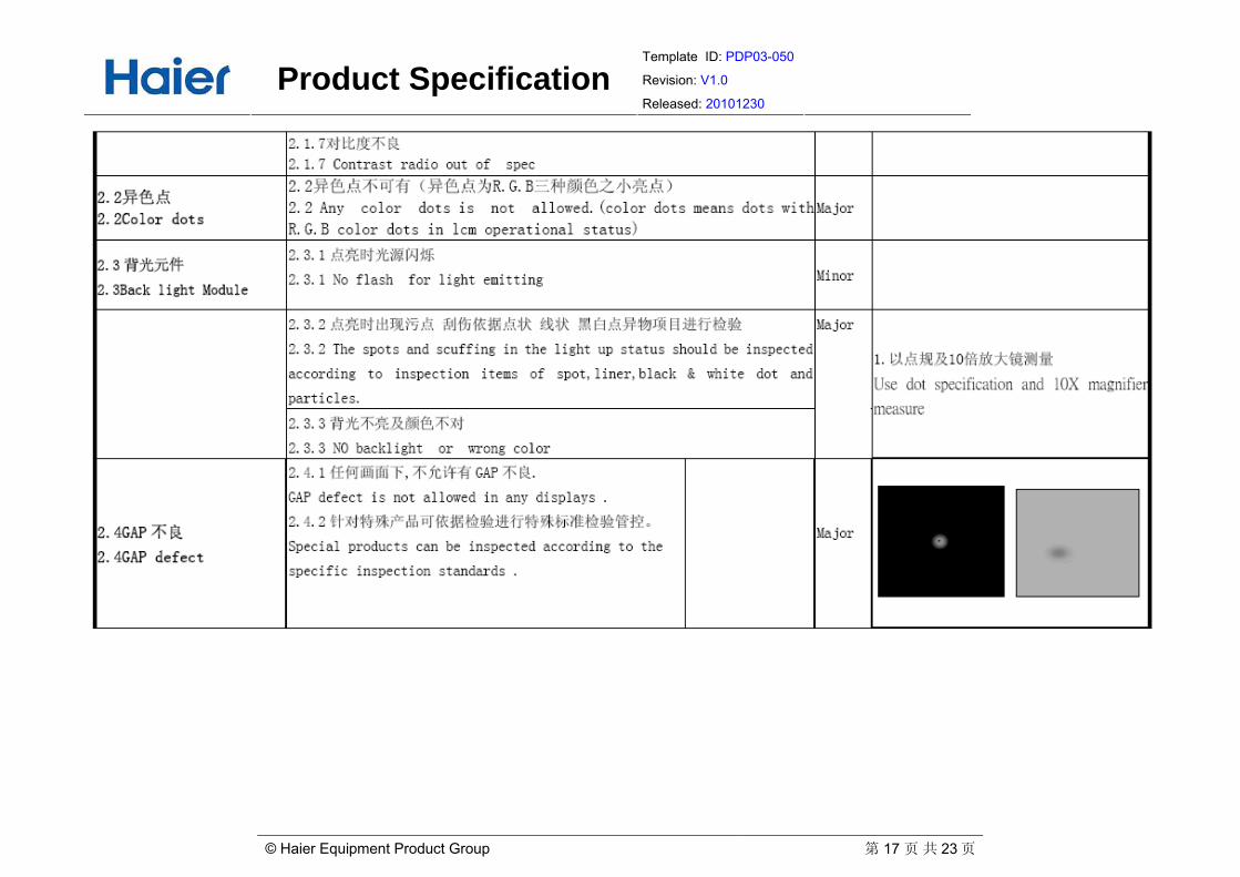
12、LCM PRODUCT INSPECTION CRITERIA

Template ID: PDP03-050
Revision: V1.0 Product Specification
Released: 20101230
© Haier Equipment Product Group 第 14 页 共 23 页

Template ID: PDP03-050
Revision: V1.0 Product Specification
Released: 20101230
© Haier Equipment Product Group 第 15 页 共 23 页

Template ID: PDP03-050
Revision: V1.0 Product Specification
Released: 20101230
© Haier Equipment Product Group 第 16 页 共 23 页
Template ID: PDP03-050
Revision: V1.0 Product Specification
Released: 20101230
© Haier Equipment Product Group 第 17 页 共 23 页

Template ID: PDP03-050
Revision: V1.0 Product Specification
Released: 20101230
© Haier Equipment Product Group 第 18 页 共 23 页

Template ID: PDP03-050
Revision: V1.0 Product Specification
Released: 20101230
© Haier Equipment Product Group 第 19 页 共 23 页

Template ID: PDP03-050
Revision: V1.0 Product Specification
Released: 20101230
© Haier Equipment Product Group 第 20 页 共 23 页

Template ID: PDP03-050
Revision: V1.0 Product Specification
Released: 20101230
© Haier Equipment Product Group 第 21 页 共 23 页

Template ID: PDP03-050
Revision: V1.0 Product Specification
Released: 20101230
© Haier Equipment Product Group 第 22 页 共 23 页

Template ID: PDP03-050
Revision: V1.0 Product Specification
Released: 20101230
© Haier Equipment Product Group 第 23 页 共 23 页