2020 trial run examination
TRANSCRIPT
2020 Trial Run Examination
A Special Test based of Extended Past Paper Models
(Internal Use Only at Hampton School)
Developed by: G. David • Bö§Zïk Inc.™
SUBJECT : PHYSICS July 30, 2020 LEVEL (Class) : Advanced (U6) 90 Minutes TEST TYPE : Paper 1 - Multiple Choice (Module 2 only)
This document consists of typeset pages and 0 blank pages. 17
Please Turn Over
..: Runtime Revision Sessions (R2S) • Navigate™ :..
READ THESE INSTRUCTIONS FIRST: • Write your name, shade your class ID on the Answer Sheet in the spaces provided unless this has
been done for you.
• Read the instructions on the Answer Sheet very carefully. Do not write in any barcodes. • There are 45 questions on this paper. Answer all questions. For each question there are four
possible answers A, B, C and D. Choose the one you consider correct and record your choice in the separate Answer Sheet provided.
• Please SHADE your MCQ responses on R2S Form A or TYPESET using R2S Form B provided. • Mark scheme [ Correct (1 mark); Incorrect (0 mark); No Response (0 mark) ] • Any rough working should be done in this booklet. Do not do any rough working on your Answer
Sheet.
• Use only a No. 2 pencil. Do not use staples, paper clips, glue or correction fluid. • Electronic calculators may be used.
CAPE: Unit 2 - Physics - 2018 TR
G. David • BÖ§ZïK Inc.™ 1 0 1 0 1 0 1 0 1

- -2
REPOSITORY OF PHYSICAL CONSTANTS
LIST OF PHYSICAL CONSTANTS
Universal gravitational constant
Acceleration due to gravity
Radius of the Earth
G
g
RE
=
=
=
6.67 x 10⁻¹¹ N m2 kg-2
9.80 m s –2
6380 km
Mass of the Earth
Mass of the Moon
Atmosphere
ME
MM
Atm
=
=
=
5.98 x 10 24 kg
7.35 x 10 22 kg
1.00 x 10 5 N m –2
Boltzmann's constant
k
=
1.38 x 10 -23 J K –1
Coulomb constant
=
9.00 x 10 9 N m 2 C –2
Mass of the electron Electron charge
me
e
=
=
9.11 x 10 -31 kg
1.60 x 10 -19 C
Density of water
Resistivity of steel
Resistivity of copper
=
=
=
1.00 x 10 3 kg m –3
1.98 x 10 -7 Ωm
1.80 x 10 -8 Ωm
Thermal conductivity of copper
=
400 W m -1 K –1
Specific heat capacity of aluminium
=
910 J kg -1 K –1
Specific heat capacity of copper
=
387 J kg -1 K –1
Specific heat capacity of water
=
4200 J kg -1 K –1
Specific latent heat of fusion of ice
=
3.34 x 10 5 J kg-1
Specific latent heat of vaporisation of water
=
2.26 x 10⁶ J kg-1
Avogadro number
Speed of light in free space
Permeability of free space
NA
c
µ0
=
=
=
6.02 x 10 23 per mole
3.00 x 10⁸ m s-1
4π x 10-7 H m-1
78CXC A16/U2/07
A-Level Physics for U6 G. David Boswell | BÖ§ZïK Inc.™ 2020 R2S Navigate

- -3
REPOSITORY OF PHYSICAL CONSTANTS (continued)
Please Do Not Turn this Page … until told
LIST OF PHYSICAL CONSTANTS (cont’d)
Permittivity of free space Ⴆ0 = 8.85 x 10⁻¹² F m-1
The Planck constant
h
=
6.63 x 10⁻³⁴ J s
Unified atomic mass constant
u
=
1.66 x 10⁻²⁷ kg
Rest mass of proton
Molar gas constant
Stefan- Boltzmann constant
mp
R
Ⴔ
=
=
=
1.67 x 10⁻²⁷ kg
8.31 J K-1 mol-1
5.67 x 10⁻⁸ W m-2 K-4
Mass of neutron
mn
=
1.67 x 10⁻²⁷ kg
79CXC A16/U2/07 A-Level Physics for U6 G. David Boswell | BÖ§ZïK Inc.™ 2020 R2S Navigate

- -4
6 Questions (01 - 06): Alternating Currents
1. A current waveform is given by the equation A. What is its
frequency, f: (A) (B) (C) (D)
2. The period of a periodic signal is What is its frequency in ?
(A) (B) (C) (D)
3. What is relationship between the peak to peak value of an alternating voltage with DC offset to the value of its true average (r.m.s.)?
(A)
(B)
(C)
(D)
4. A current is passed through an electric heater whose power rating is . What is the value of the resistance of the heater?
(A) (B) (C) (D)
5. Which if the following is TRUE in regard to the advantages of using alternating current and high voltage (HV) transmission of electrical energy?
I. Better for the environment II. Ease of transformation without loss of “Power Quality” of the AC sinusoids III. Faster delivery to the consumers IV. HV transmission with lowered current results in less losses in the transmission lines
(A) I and III (B) II and IV (C) II and III (D) III and IV
6. The peak power (in units of watts) in an AC circuit with a purely restive load can be computed using
(A) (C)
(B) (D)
11 Questions (07 - 17): The p-n Junction Diode
7. In diffusing relatively small concentrations of Boron, a Group 3 nonmetallic solid, into pure Germanium, what type of extrinsic semiconductor is produced?
(A) n-type with minority electrons (B) p-type with majority holes (C) n-type with majority electrons (D) p-type with majority protons
i(t) = 25cos(300t + 0.25)+ 8
95.5 Hz300 Hz47.7 Hz0.25 Hz
100 mskHz
10−1 Hz10−2 Hz10−3 Hz10−4 Hz
0V
Vpp =Vrms2
Vpp =2
VrmsVpp = 2Vrms
Vpp = 2 2Vrms
i(t) = 28.3sin 100t( )
4kW
10 Ω200 Ω141 Ω≈ 5 Ω
I 2R
PR =12VPIP PR =VPIP
PR =12VrmsIrms PR =
VrmsIrms2
A-Level Physics for U6 G. David Boswell | BÖ§ZïK Inc.™ 2020 R2S Navigate

- -5
8. In a p-n junction device, a ‘small p.d.’ exist across its junction. This barrier p.d. ______ .
(A) prevents the device from conducting (B) allows the device to conduct electricity in one direction only (C) controls the width of the depletion layer (D) is a result if an opposing electric field when the p-n junction is forward biased
9. The barrier p.d. for a typical p.n. junction diode made from doped intrinsic silicon is
. When the diode is operating in reversed biased and the applied p.d. is greater than its PIV at ‘avalanche breakdown’, the voltage drop across the diode is
(A) (B) (C) (D)
10. Avalanche breakdown in a p-n junction diode occurs when:
(A) Potential barrier is reduced to zero. (B) Forward current exceeds certain value. (C) Reverse bias potential exceeds a certain physical limit of the device. (D) The depletion layer widens
11. The most common uses of the p-n junction are as
(A) DC to AC converters and transistors (B) logic gates and DC filters (C) AC filters and transistors (D) diodes and transistors
12. Which of the following graph represents the correct relationship between voltage and current for a p-n junction diode?
0.7V
VD = 0.7 VVD > 0.7 VVD < 0 VVD ≈ 0 V
A-Level Physics for U6 G. David Boswell | BÖ§ZïK Inc.™ 2020 R2S Navigate
- -6
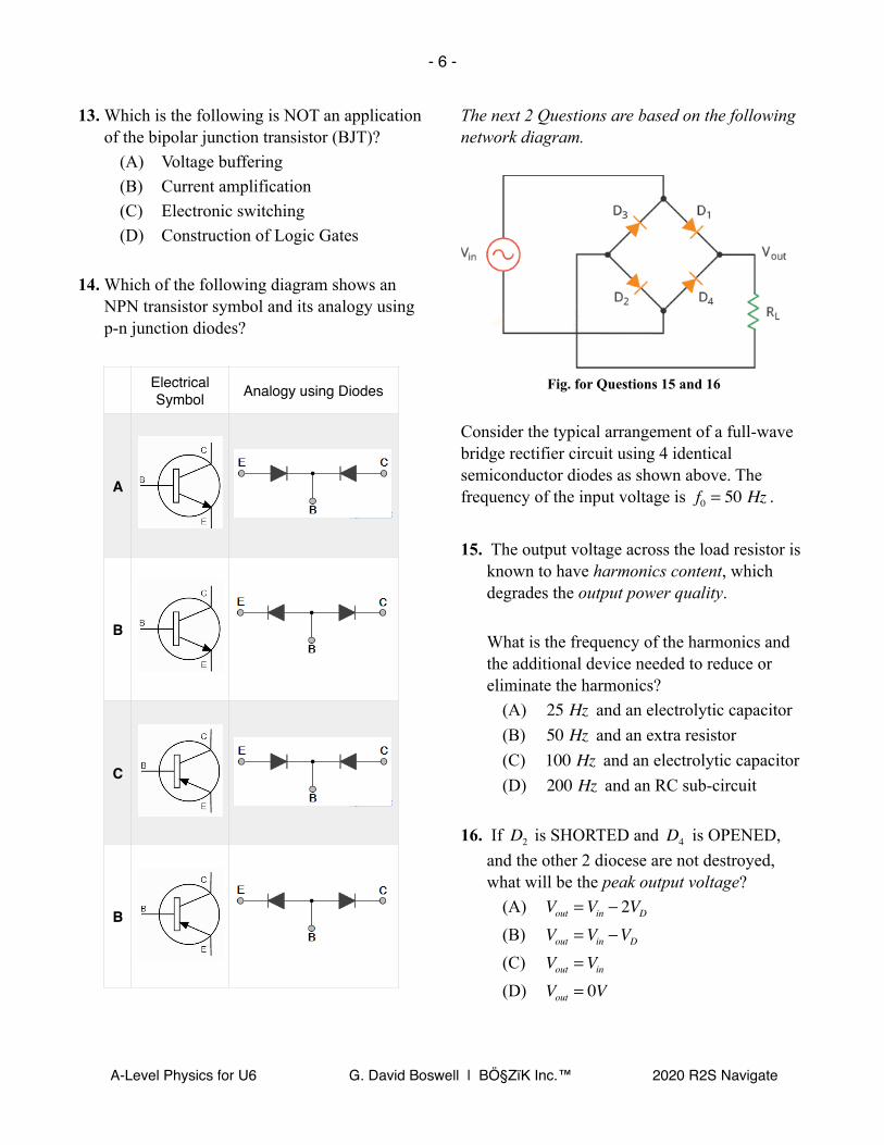
13. Which is the following is NOT an application of the bipolar junction transistor (BJT)?
(A) Voltage buffering (B) Current amplification (C) Electronic switching (D) Construction of Logic Gates
14. Which of the following diagram shows an NPN transistor symbol and its analogy using p-n junction diodes?
The next 2 Questions are based on the following network diagram.
Fig. for Questions 15 and 16
Consider the typical arrangement of a full-wave bridge rectifier circuit using 4 identical semiconductor diodes as shown above. The frequency of the input voltage is .
15. The output voltage across the load resistor is known to have harmonics content, which degrades the output power quality.
What is the frequency of the harmonics and the additional device needed to reduce or eliminate the harmonics?
(A) and an electrolytic capacitor (B) and an extra resistor (C) and an electrolytic capacitor (D) and an RC sub-circuit
16. If is SHORTED and is OPENED, and the other 2 diocese are not destroyed, what will be the peak output voltage?
(A) (B) (C) (D)
Electrical Symbol Analogy using Diodes
A
B
C
B
7/30/20, 12)18Bipolar Transistor Tutorial, The BJT Transistor
Page 4 of 25https://www.electronics-tutorials.ws/transistor/tran_1.html
Bipolar Transistor Construction
The construction and circuit symbols for both the
PNP and NPN bipolar transistor are given above
with the arrow in the circuit symbol always
showing the direction of “conventional current
flow” between the base terminal and its emitter
terminal. The direction of the arrow always points
from the positive P-type region to the negative N-
type region for both transistor types, exactly the
same as for the standard diode symbol.
Bipolar Transistor Configurations
f0 = 50 Hz
25 Hz50 Hz100 Hz200 Hz
D2 D4
Vout =Vin − 2VDVout =Vin −VDVout =VinVout = 0V
A-Level Physics for U6 G. David Boswell | BÖ§ZïK Inc.™ 2020 R2S Navigate

- -7
17. In the circuit shown, given that , , and , what is
the minimum and maximum output voltages of the circuit, respectively?
Fig. for Question 15
(A) ,
(B) ,
(C) ,
(D) ,
5 Questions (18 - 22): Transducers
18. Which of the following is an example of an input / output transducer pair, respectively?
(A) LDR / Thermistor (B) Lamp / Electromagnetic Relay (C) Piezoelectric Buzzer / LED (D) Photocell / Bell
19. And electromagnetic relay is an important transducer.
Which of the following is TRUE?
I. It requires high currents to operate efficiently. II. It can be used to create electrical isolation between 2 or more circuits. III. It can be used in circuits requiring over current protection. IV. It has no moving parts.
(A) I only (B) II only (C) II and III (D) All of the above
20. When the thermistor in the potential divider shown is cold, its resistance is .
Fig. for Question 19
As its temperature rises, its resistance decreases and the potential at node changes from
(A) to a positive value (B) to a negative value (C) to a larger value (D) to a smaller value
Vi = ±10VVD = 0.7V RL = 2Ω VB = 5V
V0min = −9.3 V V0
max = 0.7 V
V0min = −10 V V0
max = 5 V
V0min = −9.7 V V0
max = 4.3 V
V0min = 0 V V0
max = 5 V
1.0 kΩ
+9 V −9 VQ
R = 2.0 kΩRT
Q
0 V0 V
+3 V+3 V
A-Level Physics for U6 G. David Boswell | BÖ§ZïK Inc.™ 2020 R2S Navigate

- -8
21. Consider the following diagram of a Light-Dependent Resistor (LDR).
Fig. for Question 20
With the LDR in complete darkness, its p.d. is . When fully illuminated, the voltage across it drops to .
What will be the current through the resistor at that time? (Assume that when the LDR is in complete darkness, its resistance is infinite.)
(A) (B) (C) (D)
22. The diagram shows part of a circuit used to switch street lamps on and off automatically.
Fig. for Question 20
In the evening, it gets dark.
Which row shows the effect on the resistance of the light-dependent resistor (LDR) and on the potential difference (p.d.) across it?
13 Questions (23-35): Operational Amplifiers
+9 V −9 VQ
R = 2.0 kΩRT
R = 2.0 kΩIR
VSLDR
10 V3 V
2.0 kΩ
3.5 mA350 µA5 mA7 mA
14
© UCLES 2016 0625/21/M/J/16
31 The diagram shows a combination of logic gates.
input P(= 0) output X
output Yinput Q(= 1)
Input P is at a logic state 0 (low) and input Q is at a logic state 1 (high).
What are the logic states at output X and at output Y?
output X output Y
A 0 0
B 0 1
C 1 0
D 1 1
32 The diagram shows part of a circuit used to switch street lamps on and off automatically.
+
–
LDR
In the evening it gets dark.
Which row shows the effect on the resistance of the light-dependent resistor (LDR) and on the
potential difference (p.d.) across it?
resistance of LDR p.d. across LDR
A decreases decreases
B decreases increases
C increases decreases
D increases increases
A-Level Physics for U6 G. David Boswell | BÖ§ZïK Inc.™ 2020 R2S Navigate

- -9
23. What types of op-amps configuration is/are required to implement the equation below:
I. Inverting op-amp II. Non-inverting op-amp III. Voltage follower IV. Inverting Summer
(A) I and IV only (B) I and II only (C) II only (D) I only
The next 3 Questions are based on the following network diagram.
Fig. for Questions 24, 25 and 26
24. What overall voltage gain of the circuit? (A) (B) (C) (D)
25. What is the value of the current, and the output voltage, ?
(A) , (B) , (C) , (D) ,
26. What would it take in order for us to convert node b to a true virtual earth?
I. Short the resistor and connect node b to earth II. Open the resistor III. Remove the first stage amplifier and connect node a to earth.
(A) I only (B) II only (C) I and II only (D) III only
27. The derived expression for the magnitude of the voltage gain of a standard non-inverting
op-amp is
(A)
(B)
(C)
(D)
V0 =Rf
R1V1 +
Rf
R2V2
⎛⎝⎜
⎞⎠⎟−V3
AAV = 3.5AAV = 17.5AAV = 8.5AAV = ∞
i0v0
7 µA 100 mV12 mA 170 mV25 µA 350 mV14 µA 20 mV
10 kΩ
10 kΩ
AV = v0 (t)vi (t)
=
Rg + Rf
RgRg − Rf
RgRg + Rf
Rf
1+RgRf
A-Level Physics for U6 G. David Boswell | BÖ§ZïK Inc.™ 2020 R2S Navigate

- -10
28. When the input to the differential terminals of a op-amp is a cosine wave, the shape of the output waveform is likely to be a ______.
(A) sinusoidal waveform (B) a saw-tooth waveform (C) a square waveform (D) a clipped sinusoidal waveform
29. Consider the transfer function of an op-amp circuit powered by a dual power supply:
A configuration to archive this function is
(A) Inverting op-amp with and
(B) Non-inverting op-amp with and
(C) Non-inverting op-amp with and
(D) Inverting op-amp with and
30. The peak value of input voltage of a op-amp circuit is and its r.m.s. output is
. Compute the voltage gain, (A) (B) (C) (D)
31. Consider an Open Loop Gain-Frequency Response for an op-amp as shown.
Fig. for Question 31
What is the value of the Gain-Bandwidth Product (GBWP) of the same op-amp circuit when its closed loop voltage gain is 100?
(A) (B) (C) (D)
32. At the maximum bandwidth of an operational amplifier (op-amp) in a circuit with a frequency-caring input signal, the voltage gain of the amplifier is
(A) 0 (B) 1 (C) (D)
±25V
VOUT =−25 , VIN > +2.5 volts
−10VIN , −2.5 <VIN < +2.5 volts+25 , VIN < −2.5 volts
⎧
⎨⎪
⎩⎪⎪
Rf = 10 kΩ Ri = 100 kΩ
Rf = 470 kΩ Rg = 47 kΩ
Rf = 56 kΩ Rg = 560 kΩ
Rf = 10 kΩ Ri = 1 kΩ
12 V283 mV AV (dB)
20 log10 30.0 dB10 log10 30.0 dB20 log10 42.4 dB10 log10 42.4 dB
7/30/20, 09)28Op Amp Bandwidth: Operational Amplifier Frequency Response » Electronics Notes
Page 1 of 7https://www.electronics-notes.com/articles/analogue_circuits/operational-amplifier-op-amp/gain-bandwidth-product-frequency-response.php
!
Op-Amp Bandwidth, Gain Bandwidth Product &Frequency ResponseThe bandwidth of an operational amplifier is a key factor in its performance and itis directly related to the gain bandwidth product .
Op-amp Tutorial Includes:Introduction Op amp gain Bandwidth Op amp slew rate Offset null Input impedance Outputimpedance Understanding specifications How to choose an op amp Op amp circuits summary
The bandwidth of any circuit is of paramount importance that needs to be considered during the electroniccircuit design process.
When designing the electronic circuit, it will be seen that the bandwidth of the circuit is related to the gain. Toomuch gain and the bandwidth will be low, less gain and the bandwidth that can be achieved is much higher.
As any op amp has limited bandwidth, it is necessary to carefully consider the gain, bandwidth, and frequencyresponse at the outset of the design of any circuit.
Operational amplifiers themselves when operating in open loop mode only have a very limited limitedbandwidth before the gain starts to fall. However by using negative feedback, the huge gain of the amplifier canbe used to ensure that a flat response with sufficient bandwidth is available.
Op amp bandwidthAlthough op amps have a very high gain, this level of gain starts to fall at a low frequency. The open loopbreakpoint, i.e. the frequency at which the gain has fallen by 3 dB is often only a few Hz.
The long lived and still very popular 741 op amp has an open loop breakpoint around 6Hz. Beyond this theresponse falls at a rate of -6dB/octave or -20dB/decade. Note: an octave is a doubling in frequency, and adecade is a ten-fold increase in frequency and therefore these two figures are two ways of expressing the samecharacteristic.
1 10 10 10 10 10 102 3 4 5 61
10
102
103
104
105
106
Ope
n Lo
op V
olta
ge g
ain
Frequency (Hz)
" # $
FOLLOW
30 JULY 2020
Fact of the day: It was on this day in 1889that Vladimir Zworykin was born in Russia. Heinvented the iconoscope and as a result wasoften called the 'Father of Television.' on thisday in 1959 that Robert Noyce's patent forintegrated circuit technology was filed in theUSA. Along with Jack Kilby's ideas and patentthis started the age of semiconductorintegration.
Quote: I never think of the future; it comes soonenough Albert Einstein
Fact: Michael Faraday who discovered manyof the basic foundations of electrical sciencewas the son of a blacksmith and received littleformal education.
FOCUS ON TEST
Focus on Test from Rohde &Schwarz offers a huge number ofinformative PDFs, white-papers,webinars videos and general information onmany test topics. Rohde &Schwarz Focus on Test Zone.
HOME ELECTRONICS COMMUNICATIONS TEST EQUIPMENT HISTORY RESOURCES SHOPPING
0.8 Hz102 Hz103 Hz106 Hz
106
∞
A-Level Physics for U6 G. David Boswell | BÖ§ZïK Inc.™ 2020 R2S Navigate

- -11
The next 2 Questions are based on the following network diagram.
33. An operational amplifier (op-amp) is used in the comparator circuit shown below.
Fig. for Questions 33 and 34
What is the value of the potential at the inverting input of the op-amp?
(A) (B) (C) (D)
34. Under what condition is the potential difference across the resistor is ? (A) (B) (C) (D)
20
9702/41/M/J/15© UCLES 2015
Section B
Answer all the questions in the spaces provided.
10 An operational amplifier (op-amp) is used in the comparator circuit of Fig. 10.1.
V IN V OUT1.2 k1
4.2 k1
R–5 V
+5 V
+4.5 V
+
–
Fig. 10.1
(a) (i) Show that the potential at the inverting input of the op-amp is +1.0 V.
[1]
(ii) Explain why the potential difference across resistor R is + 5 V when VIN is greater than 1.0 V and is zero when VIN is less than 1.0 V.
VIN > 1.0 V: .........................................................................................................................
...........................................................................................................................................
...........................................................................................................................................
VIN < 1.0 V: .........................................................................................................................
...........................................................................................................................................
...........................................................................................................................................[4]
+1.0 V−1.0 V+4.5 V+2.25 V
VOUT = 0VVIN < +1.0 VVIN ≤ −1.0 VVIN > +4.5 V−5 <VIN < 5 V
A-Level Physics for U6 G. David Boswell | BÖ§ZïK Inc.™ 2020 R2S Navigate

- -12
35. The circuit diagram for a temperature-sensing device is shown. The operational amplifier is assumed to be ideal. G and B represents green and blue light LEDs, respectively.
Fig. for Question 35
Thermistor Calibration Data or Question 35
The thermistor is held in a water bath at a temperature of and based on its Calibration Curve, is temperature is
What are states of the 2 LEDS at ?
G B (A) OFF OFF (B) OFF ON (C) ON OFF (D) ON ON
14
9702/04/SP/16© UCLES 2014
7 (a) The symbol for a light-emitting diode (LED) is shown in Fig. 7.1.
Fig. 7.1
On Fig. 7.1, mark the polarity of the diode such that the diode is emitting light. [1]
(b) The circuit diagram for a temperature-sensing device is shown in Fig. 7.2.
Fig. 7.2
The operational amplifi er (op-amp) is ideal.
Some values for the resistance of the thermistor at different temperatures are given in Fig. 7.3.
temperature / ° C resistance / Ω
15
30
60
100
2200
1200
800
680
Fig. 7.3
The thermistor is held in a water bath at a temperature of 15 °C.
14
9702/04/SP/16© UCLES 2014
7 (a) The symbol for a light-emitting diode (LED) is shown in Fig. 7.1.
Fig. 7.1
On Fig. 7.1, mark the polarity of the diode such that the diode is emitting light. [1]
(b) The circuit diagram for a temperature-sensing device is shown in Fig. 7.2.
Fig. 7.2
The operational amplifi er (op-amp) is ideal.
Some values for the resistance of the thermistor at different temperatures are given in Fig. 7.3.
temperature / ° C resistance / Ω
15
30
60
100
2200
1200
800
680
Fig. 7.3
The thermistor is held in a water bath at a temperature of 15 °C. 150C
2.2kΩ
150C
A-Level Physics for U6 G. David Boswell | BÖ§ZïK Inc.™ 2020 R2S Navigate
- -13
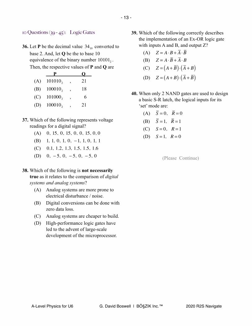
10 Questions (39 - 45): Logic Gates
36. Let P be the decimal value converted to base 2. And, let Q be the to base 10 equivalence of the binary number . Then, the respective values of P and Q are
P Q (A) , 21 (B) , 18 (C) , 6 (D) , 21
37. Which of the following represents voltage readings for a digital signal?
(A) (B) (C) (D)
38. Which of the following is not necessarily true as it relates to the comparison of digital systems and analog systems?
(A) Analog systems are more prone to electrical disturbance / noise. (B) Digital conversions can be done with zero data loss. (C) Analog systems are cheaper to build. (D) High-performance logic gates have led to the advent of large-scale development of the microprocessor.
39. Which of the following correctly describes the implementation of an Ex-OR logic gate with inputs A and B, and output Z?
(A) (B) (C)
(D)
40. When only 2 NAND gates are used to design a basic S-R latch, the logical inputs for its ‘set’ mode are:
(A) (B) (C) (D)
(Please Continue)
3410
101012
1010102100010210100021000102
0, 15, 0, 15, 0, 0, 15, 0, 01, 1, 0, 1, 0, −1, 1, 0, 1, 10.1, 1.2, 1.3, 1.5, 1.5, 1.60, − 5, 0, − 5, 0, − 5, 0
Z = A ⋅B + A ⋅BZ = A ⋅B + A ⋅BZ = A + B( ) ⋅ A + B( )Z = A + B( ) ⋅ A + B( )
S = 0, R = 0S = 1, R = 1S = 0, R = 1S = 1, R = 0
A-Level Physics for U6 G. David Boswell | BÖ§ZïK Inc.™ 2020 R2S Navigate

- -14
41. The diagram shows a combination of logic gates.
Fig. for Question 41
Input P is at a logic state 0 (low) and input Q is at a logic state 1 (high). What are the logic states at output X and at output Y?
(A) (B) (C) (D)
42. Consider the following 4-input digital circuit shown.
Fig. for Question 42
When A = C = 0 and B = D = 1, what are intermediate states R and the final output Z?
(A) (B) (C) (D)
14
© UCLES 2016 0625/21/M/J/16
31 The diagram shows a combination of logic gates.
input P(= 0) output X
output Yinput Q(= 1)
Input P is at a logic state 0 (low) and input Q is at a logic state 1 (high).
What are the logic states at output X and at output Y?
output X output Y
A 0 0
B 0 1
C 1 0
D 1 1
32 The diagram shows part of a circuit used to switch street lamps on and off automatically.
+
–
LDR
In the evening it gets dark.
Which row shows the effect on the resistance of the light-dependent resistor (LDR) and on the
potential difference (p.d.) across it?
resistance of LDR p.d. across LDR
A decreases decreases
B decreases increases
C increases decreases
D increases increases
X = 0, Y = 0X = 0, Y = 1X = 1, Y = 0X = 1, Y = 1
P
Q R
Z
A
B
C
D
R = 0, Z = 0R = 0, Z = 1R = 1, Z = 0R = 1, Z = 1
A-Level Physics for U6 G. David Boswell | BÖ§ZïK Inc.™ 2020 R2S Navigate

- -15
43. A 4-output binary circuit X was used to generate signals , , and below. The input to the circuit was a uniform set of clock signal (pulses).
Fig. for Question 43
Which of the following is correct?
I. Circuit X is called a Synchronous Ripple Binary Counter. II. The output data change on the rising edge of the clock pulse. III. T-Flip Flops cannot be used to build Circuit X.
(A) I only (B) I and II only (C) II and III only (D) I, II and III
(Please Continue)
QA QB QC QD
A-Level Physics for U6 G. David Boswell | BÖ§ZïK Inc.™ 2020 R2S Navigate
- -16
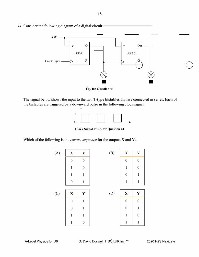
44. Consider the following diagram of a digital circuit.
Fig. for Question 44
The signal below shows the input to the two T-type bistables that are connected in series. Each of the bistables are triggered by a downward pulse in the following clock signal.
Clock Signal Pulse. for Question 44
Which of the following is the correct sequence for the outputs X and Y?
+9 V −9 VQ
R = 2.0 kΩRT
R = 2.0 kΩIR
VSLDR
Q Q
Q Q
T T
+5V
YX
FF #1 FF #2
Clock input
+9 V −9 VQ
R = 2.0 kΩRT
R = 2.0 kΩIR
VSLDR
Q Q
Q Q
T T
+5V
YX
FF #1 FF #2
Clock input
0
1
(A) X Y
0 0
1 0
1 1
0 1
(B) X Y
0 0
1 0
0 1
1 1
(C) X Y
0 1
0 1
1 1
1 0
(D) X Y
0 0
0 1
1 0
1 1
A-Level Physics for U6 G. David Boswell | BÖ§ZïK Inc.™ 2020 R2S Navigate

- -17
45. In a 3-bit binary counter using T flip-flops, the clock frequency is 240 Hz. If its LSB and MSB are bits and , respectively, what is the frequency of bit ?
(A) 120 Hz (B) 240 Hz (C) 60 Hz (D) 30 Hz
- ENFIN -
Q0 Q2
Q1
A-Level Physics for U6 G. David Boswell | BÖ§ZïK Inc.™ 2020 R2S Navigate