2011 inemi introduction & selected...
TRANSCRIPT
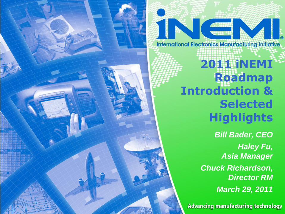
2011 iNEMI Roadmap
Introduction & Selected
Highlights
Bill Bader, CEO
Haley Fu,
Asia Manager
Chuck Richardson,
Director RM
March 29, 2011

Asian Agenda
Time Subject Presenter
8:00 AM iNEMI Welcome/Roadmap Overview Bill Bader, Haley Fu,
8:15 AM Portable, Auto and Medical product sectors Chuck Richardson,
8:30 AM Packaging & Component Substrates Chuck Richardson
8:40 AM Board Assembly Paul Wang, Mitac
8:55 AM Test, Inspection & Measurement Bill Bader
9:05 AM Environmentally Conscious Electronics Haley Fu
9:15 AM Summary Bill Bader
9:25 AM Q & A, Discussion Haley Fu, All
9:30 AM Close
1
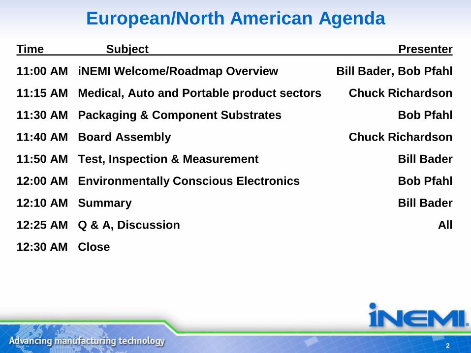
European/North American Agenda
2
Time Subject Presenter
11:00 AM iNEMI Welcome/Roadmap Overview Bill Bader, Bob Pfahl
11:15 AM Medical, Auto and Portable product sectors Chuck Richardson
11:30 AM Packaging & Component Substrates Bob Pfahl
11:40 AM Board Assembly Chuck Richardson
11:50 AM Test, Inspection & Measurement Bill Bader
12:00 AM Environmentally Conscious Electronics Bob Pfahl
12:10 AM Summary Bill Bader
12:25 AM Q & A, Discussion All
12:30 AM Close

International Electronics Manufacturing Initiative (iNEMI)• Not for profit, highly efficient R&D consortia since 1994
– Funded by Corporate memberships - Staffed globally in US, China & Ireland
• Membership includes 89 leading industry companies & organizations, representing
a cross section of our electronics manufacturing industry & supply chain
3
iNEMI Mission: Forecast and accelerate improvements in the Electronics Manufacturing
Industry for a sustainable future.
We Accomplish This By:
• Being the recognized leader at projecting future technology needs for the global supply
chain (iNEMI Technology Roadmap).
• Guiding and leveraging the strength of the consortium‟s industry leading international
membership.
• Driving high impact collaborative R&D Results through constantly improving methodologies.
• Defining and implementing science based sustainable solutions in high impact areas
including the environment and health care.
• Influencing and leveraging key government agencies and labs (iNEMI Research Priorities
Document).
• iNEMI has currently 25 collaborative R&D projects and initiatives that address key
technology gaps
• Projects typically have 10-20 member companies/institutions
www.inemi.org

Roadmap Process & Scope

Some Definitions
• TWG - Technical Working Group
– Develops the roadmap technology chapters
– Presently 21 groups and chapters
• PEG – Product Emulator Group
– “Virtual Product”: future product attributes plus key cost and density
drivers
• Portable / Consumer
• Office / Large Business Systems
• Netcom Systems
• Medical Products
• Automotive
• Aerospace/Defense
5
Methodology
6
Product
Needs
Technology
Evolution
GAP
AnalysisResearch
Projects
Competitive
Solutions
Roadmap
Industry Solution
Needed
Academia
Government
iNEMI
Members
Collaborate
No Work
Required
Available
to Market
Place
Global
Industry
Participation Disruptive
Technology

Statistics for the 2011 Roadmap
• > 575 participants -- Big Thanks to All Contributors!!
• > 310 companies/organizations
• 18 countries from 4 continents
• 21 Technology Working Groups (TWGs)
• 6 Product Emulator Groups (PEGs)
• > 1800 pages of information
• Roadmaps the needs for 2011-2021
• Workshops held in Europe (IMEC, Belgium), Asia (TPCA, Taiwan) and North America (ECTC, Las Vegas) in June 2010
• A Full Global Perspective
• Available to iNEMI members on 12/22/10 at: www.inemi.org
• Available to industry beginning March 29 at www.inemi.org
7

2011 Technology Working Groups (TWGs)
8
Organic PCBBoard
Assembly Customer
RF Components &
Subsystems
OptoelectronicsLarge Area, Flexible Electronics
Energy Storage &
Conversion Systems
Modeling, Simulation,
and Design
Packaging
&
Component
Substrates
Semiconductor
Technology
Final
Assembly
Mass Storage (Magnetic & Optical)
Passive Components
Information
Management
Systems
Test, Inspection &
Measurement
Environmentally
Conscious
Electronics
Ceramic
Substrates
Thermal
Management
Connectors
MEMS/
Sensors
Red=Business Green=Engineering Aqua=Manufacturing Blue=Component & Subsystem
Solid State Illumination
Photovoltaics

Roadmap Development
9
Product Emulator GroupsTWGs
Med
ical P
rod
ucts
Au
tom
oti
ve
Defe
nse a
nd
Aero
sp
ace
Semiconductor Technology
Design Technologies
Manufacturing Technologies
Comp./Subsyst. Technologies
Modeling, Thermal, etc.
Board Assembly, Test, etc.
Packaging, Substrates, Displays, etc.
Product Sector Needs Vs. Technology Evolution
Business Processes
Prod Lifecycle Information Mgmt.
Po
rtab
le / C
on
su
me
r
Off
ice / L
arg
eS
yste
ms
Netc
om
Optoelectronics and
Optical Storage
Organic Printed
Circuit Boards
Magnetic and
Optical Storage
Supply Chain
Management
Semiconductors
iNEMI
Information
Management
TWG
iNEMI
Mass Data
Storage TWG
iNEMI / IPC / EIPC
/ TPCA
Organic PWB
TWG
iNEMI / ITRS /
MIG/PSMA
Packaging
TWG
iNEMI
Board Assembly
TWG
Interconnect
Substrates—Ceramic
iNEMI Roadmap
iNEMI
Optoelectronics
TWG
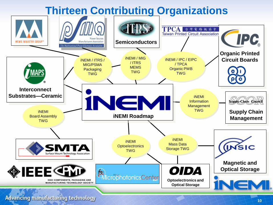
Thirteen Contributing Organizations
10
iNEMI / MIG
/ ITRS
MEMS
TWG

Situation Analysis
• Convergence
– Medical-Consumer
– Automotive-Entertainment
– Communication-Entertainment
• Telecom-Datacom
• Miniaturization and Thinner; Speed of Change Escalating
• Quality, reliability, cost still paramount
• Counterfeit Products a growing issue
• Product Personalization
• Infrastructure (Business Model) changes:
– Fabless Semiconductor Fabrication
– Redundant Elements
– EMS and ODM roles grow; R&D Challenges
• Rare Earth and Conflict Materials
• Carbon foot printing is becoming a requirement
• Energy Storage
– Growth in Consumer electronics
– New transportation market
– Future opportunity for smart grid
11

Highlights of PEGs

ELECTRONICS PRODUCTION
2009 - 2021
Note: Total includes product categories not included in iNemi segmentation
$Bn 2009 2011 2013 2015 2021 CAAGR
„09-„15
CAAGR
„15-„21
Computers and Office $396 $433 $474 $500 $617 4.0% 3.6%
Communications Infrastructure Equipment $157 $174 $192 $213 $281 5.2% 4.7%
Consumer and Portable Electronics $298 $319 $341 $400 $479 5.0% 3.1%
Automotive Electronics $105 $129 $158 $161 $237 7.4% 6.6%
Medical Electronics $77 $85 $93 $103 $134 5.0% 4.5%
Military and Aerospace Electronics $118 $129 $140 $151 $189 4.2% 3.8%
Total Electronics Production $1,242 $1,382 $1,541 $1,679 $2,171 5.2% 4.4%
Courtesy PrismarK Partners LLC
13
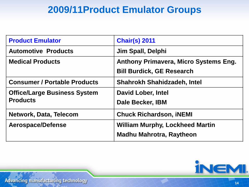
2009/11Product Emulator Groups
14
Product Emulator Chair(s) 2011
Automotive Products Jim Spall, Delphi
Medical Products Anthony Primavera, Micro Systems Eng.
Bill Burdick, GE Research
Consumer / Portable Products Shahrokh Shahidzadeh, Intel
Office/Large Business System
Products
David Lober, Intel
Dale Becker, IBM
Network, Data, Telecom Chuck Richardson, iNEMI
Aerospace/Defense William Murphy, Lockheed Martin
Madhu Mahrotra, Raytheon
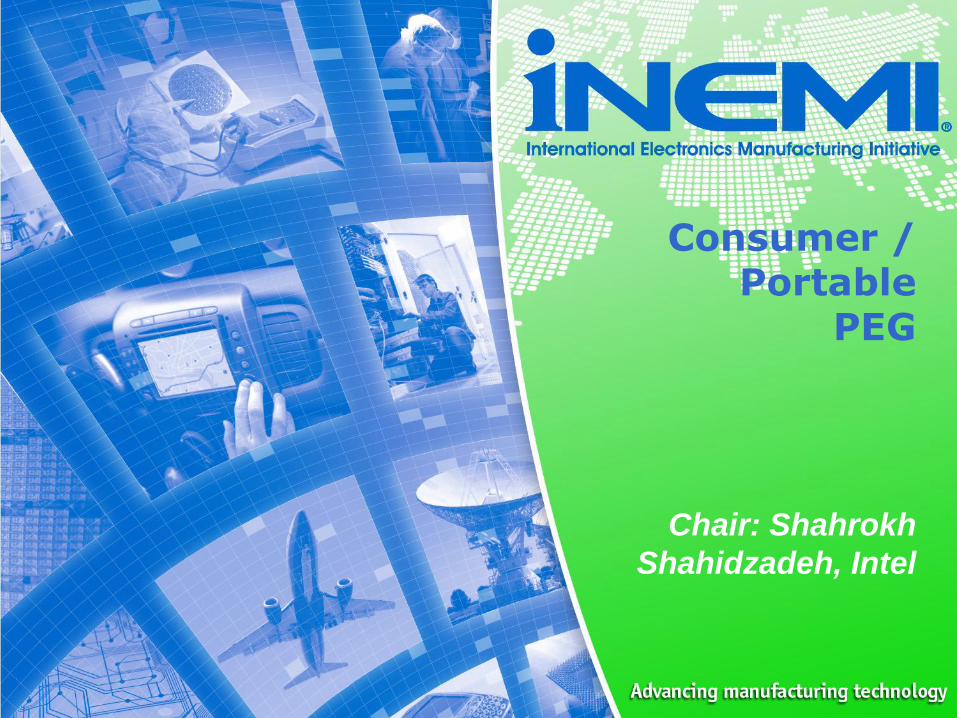
Consumer / Portable
PEG
Chair: Shahrokh
Shahidzadeh, Intel

1616
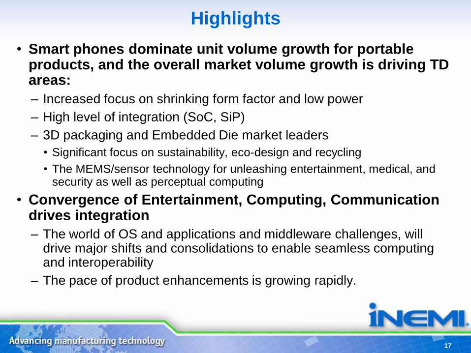
Highlights
• Smart phones dominate unit volume growth for portable products, and the overall market volume growth is driving TD areas:
– Increased focus on shrinking form factor and low power
– High level of integration (SoC, SiP)
– 3D packaging and Embedded Die market leaders
• Significant focus on sustainability, eco-design and recycling
• The MEMS/sensor technology for unleashing entertainment, medical, and security as well as perceptual computing
• Convergence of Entertainment, Computing, Communication drives integration
– The world of OS and applications and middleware challenges, will drive major shifts and consolidations to enable seamless computing and interoperability
– The pace of product enhancements is growing rapidly.
17

Automotive PEG
Chair: Jim Spall,
Delphi

• Business Issues
– Reduced North American volume in 2009 (worst year in 30 years)
– Western Europe sales tracking at a full-year rate near 14.7 million units
for 2009, 2010 volume could be reduced to 13.7 million units
– Japan sales declined to the lowest level in 38 years (2.9 million units)
– China exceeding the U.S. in auto output in 2009 (12 million units)
• Up 34 percent from a year earlier
– Increased Corporate Average Fuel Economy to 35.5 mpg by 2016
• Downsizing of engines and increased use of Gas Direct injection
• Increased use of turbo-charging
• Researchers project 14 million electrified vehicles annually by 2020
Situation Analysis
Automotive Product Emulator
19

• Technical Issues
– Shift to Hybrid Electric Vehicles (HEV), Plug-in Hybrid Electric Vehicles (PHEV), and Electric Vehicles (EV)
• Invention required to reach the battery cost target of $250/kWh
– Today‟s cost $1,000 -$1,200/kWh
• Key components that are in need include: power devices, bulk capacitors, inductors and transformers, cooling structures, motor drive microprocessors, high current connectors, current sensors, gate driver ICs, battery management ICs, bus bars, and enclosures.
– Increased use of MEMS in automotive
• Accelerometers
• Gyroscopes
• Pressure
• Air Flow
Situation Analysis (con‘t.)
Automotive Product Emulator
20

– 12.3 inch reconfigurable displays for the instrument panel
– LED lighting used internally and externally
– Connected Vehicle
• Key Drivers: cost, reliability, size
– Cost is still the key driver for automotive
• Competitive cost will get you an opportunity to win a program
– Reliability is a given in the automotive sector
• Failure to deliver will result in no future business
• Toyota situation will test its loyal customer base
– Size is a benefit because some vehicles having 100 electronic
controllers and space is limited
Situation Analysis (con‘t.)
Automotive Product Emulator
21

• Chart 2009 vs. 2011 forecast differences
– Circuit board – use of 8 layer with blind vias
– Lower memory prices in 2011 than forecast
– Increased use of MEMS sensors (Identified the types being used in the
emulator)
– Higher resolution and larger displays being used (12.3” displays for the
instrument cluster)
– Nand Flash used for Hard Drive emulation
– Increased use of Built In Self Test (BIST) and Boundary Scan
– Quicker conversion to lead free solder
– Greater thermal demands due to the electrified vehicle
Situation Analysis (con‘t.)
Automotive Product Emulator
22

Medical PEG
Chair: Anthony
Primavera, Micro
Systems Eng.
Co-chair: Bill Burdick,
GE Research

Medical Market Background
• Global
– 65+ year old population will triple by 2050 .. from 516M (2009) to 1.53B
(2050)
– 80+ year old population will increase from 40M (2009) to 219M (2050)
• Currently, the U.S. (for example) spends 1.75 Trillion dollars
… 15% of 2009 GDP … 25% of GDP 2015
• It is estimated that current annual spending on medical
devices / electronics is 70 to 100 Billion dollars
• The market opportunities are large and are growing
24

Three Major Market Sectors
25
Medical products were grouped into three general categories.
1) Implanted products (devices implanted in a human body)
– Strict regulatory procedures
– Driven by battery life (low power loss) – this limits the use of certain
components such as DRAM due to high energy consumption
– Validation and traceability required
– Long term reliability paramount
– Long development cycles, primary assembly and design by OEMs
2) Portable products (devices that are easily transported)
– Cost parity with consumer / portables
– Dynamic market, needs fast response, 9 to 24 month product cycle time
– Mixed regulatory environment
– Mostly outsourced assembly and design
– Higher Volume; Lower Cost – example – diagnostic ultrasound in PDA size ..
and smaller .. form factors
3) Diagnostic imaging devices and large scale equipment, e.g., MRI, CT
– Larger scale (often similar to servers or telecom equipment)
– Challenging thermal management and heat sinking
– Utilizes commercial off-the-shelf components, when available
– Development cycle is shorter than implantable
– Application and design well suited to EMS environment
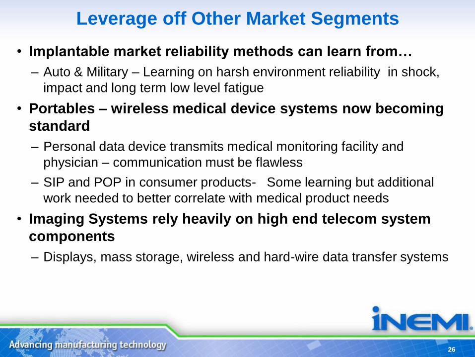
Leverage off Other Market Segments
• Implantable market reliability methods can learn from…
– Auto & Military – Learning on harsh environment reliability in shock,
impact and long term low level fatigue
• Portables – wireless medical device systems now becoming
standard
– Personal data device transmits medical monitoring facility and
physician – communication must be flawless
– SIP and POP in consumer products- Some learning but additional
work needed to better correlate with medical product needs
• Imaging Systems rely heavily on high end telecom system
components
– Displays, mass storage, wireless and hard-wire data transfer systems
26

Critical Gaps and Challenges
• Connector technologies that are highly reliable
– Ultra small for implantable products with automated wire attach. Also require
ultra high fidelity signal properties
– Large geometry connectors for imaging systems with superior contact quality –
zero electron loss
• Safety and efficacy in RF traffic wireless telemetry.
– Different frequencies, pulse widths, etc. in medical device settings are not
thoroughly addressed in international standards
• High reliability (10 year life minimum) PCB technologies to support
high density high performance silicon in implantable – major
research need
• High performance energy storage methodologies
– Includes researching and refining energy harvesting the bodies thermal and
motion attributes
• Addressing critical business issues for the medical market:
– Conversion to alternative to leaded solder attach technologies
– Simplifying regulatory and time to market challenges
27

Highlights of TWGs

2011 TWG Leadership Status
29
Business Processes /
Technologies
Chair(s) Co-Chair(s)
Information Management Jeff Pettinato, Intel Eric Simmon, NIST
Design Technologies
Modeling, Simulation &
Design Tools
Yishao Lai, ASE
Andy Tseng, ASE
S.B. Park, Binghamton U.
Environmentally Conscious
Electronics
Jackie Adams, IBM
Ted Reichelt, Intel
(Retired)
Thermal Management Azmat Malik, Consultant
Manufacturing Technologies
Final Assembly John Allen, Celestica Reijo Tuokko, Tampere U.
Board Assembly Paul Wang, Mitac Mitch Holtzer, Bawa Singh,
Cookson Electronics
Test, Inspection &
Measurement
Mike Reagin, Delphi

2011 TWG Leadership (cont.)
30
Component / Subsystem
Technologies
Chair(s) Co-Chair(s)
Semiconductor Technology Paolo Gargini, Intel Alan K. Allan, Intel
Optoelectronics Dick Otte, Promex William Ring, WSR
Photovoltaics Jim Handy Objective-Analysis Alain Harrus, Cross Link Capital
Packaging Bill Bottoms, 3MTS
William Chen, ASE
Passive Components Ed Mikoski, ECA
Connectors John MacWilliams, Consultant
RF Components Ken Harvey, Advantest Eric Strid, Cascade MicroTech
MEMS / Sensors Michael Gaitan, NIST Raffaella Borzi, IMEC
Francois Iker, IMEC
Large Area, Flexible Electronics Dan Gamota, Printovate
Technologies
Andreas Schaller, ASC
Jie Zhang, Institute of Materials
Research and Engineering
Energy Storage & Conversion
Systems
Namid Maluf, QNovo
Tom Newton, IPC
Ravi Bhatkal, Cookson Electronics
Interconnect Substrates (Ceramic) Howard Imhof, Metalor Ton Schless, Sibco
Interconnect PCB John T. Fisher, IPC
Michelle Hung, TPCA Liaison
Henry Utsunomiya, Consultant
Dieter Bergman, IPC
Mass Data Storage Roger F. Hoyt, Consultant Tom Coughlin, Coughlin Associates
Illumination Marc Chason, Consultant Ravi Bhatkal, Cookson Electronics

Packaging & Component
Substrates TWG
Chair: Bill Bottoms,
3MTS
Co-chair: William
Chen, ASE

Packaging and Component Substrate
Technical Working Group
Areas of Focus:
– Materials
– Embedded components
– 3D integration
– Wafer thinning
– Interposers
– Bonding (d-d, w-w, d-w)
– Optical interconnect for SiP
32

33
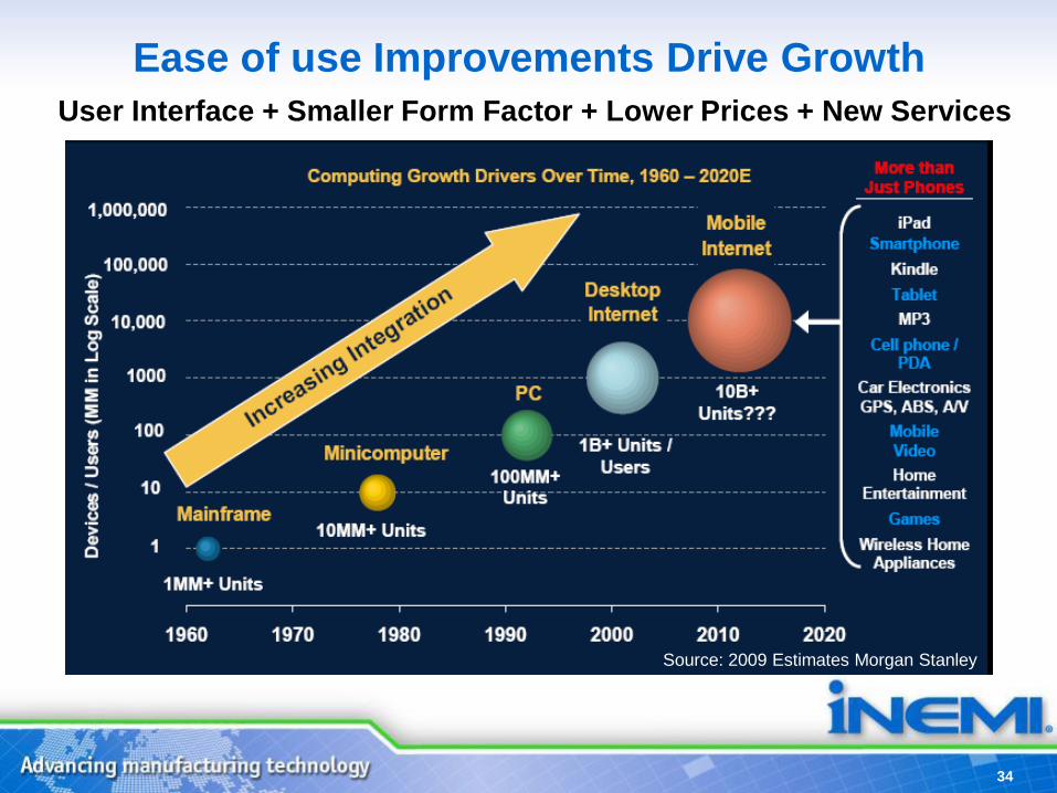
Source: 2009 Estimates Morgan Stanley
Connectivity is the Key to Consumer Growth
34
Ease of use Improvements Drive Growth
User Interface + Smaller Form Factor + Lower Prices + New Services
Source: 2009 Estimates Morgan Stanley

The Consumer dominates the Market and
The Market makes the decisions
What does the Consumer want?
– Lower cost
– Higher performance
– Longer battery life
– Innovative features
– Connectivity (wireless)
– Smaller size
– Lighter weight
– Less heat generation
– Rapid availability
35

Roadmap of Quantified Key Attribute Needs
36
Functional Diversification (―More than Moore‖) is driving rapid change in Packaging and Component Substrate Technology for Consumer products
New packaging technologies needed to satisfy market requirements include:
• Wafer level packaging
• Wafer thinning
• System in Package (SiP)
• Printed electronics
• Direct bonding interconnect
• New conducting materials
• New dielectric materials
• 3D Integration
3D integration will require a combination of new technologies and materials including some defined above

• Through Silicon Via – active wafer & interposers
• Two side wafer level Processes– RDL and MicroBumping
• Embedded Components (active & passive)
• Wafer thinning & Handling
• Wafer to Wafer Bonding
• Die to Wafer Bonding
• Micro bump assembly
• Design Tools
• Micro fluidics Cooling
• Assembly of TSV die
• Test of TSV Die
Technologies Enabling 3D Integration
Source: Phil Garrou, 2009
37

3D System Integration
38

3D System IntegrationPost Fab Processing for 3D TSV integration
provides key advantages for Consumer
products:
• Reduced power
• Increased performance
• Lighter weight
• Smaller size
39

SiP Packaging reduces cost
and time to market:
• Heterogeneous integration
• Reduced NRE
• Reduced power
• Smaller size
3D System Integration
40

Pushing the Envelope
• All of these new technologies are moving very quickly.
• In today's world the effectiveness of an integrated supply
chain approach is key
• Multiple nodes on the supply chain covering all aspects of
design, materials, assembly, test, etc, etc
• Cooperative roadmap efforts of groups (such as, MIG, iNEMI,
IPC, TPCA and ITRS) are key to clarify timing and needs
• There are many/many opportunities for collaborative R&D
– An iNEMI Strength and Core Capability
41
Board Assembly TWG
Chair: Paul Wang, Mitac
Co-Chair: Mitch Holtzer,
Bawa Singh, Cookson
Miniaturization Credits –
John Lau
43
Key Trends (2011 Roadmap)
Business Environment
• Higher level of service demand placed on EMS
• EMS companies are expanding offerings to include services
in a wider range of a product‘s life cycle
• Increased role of EMS/ODM and materials/equipment
suppliers in R&D and process development
• Continued migration to low cost regions
• Demands on cost reduction and low margins are driving
consolidation among EMS companies
43

44
Key Trends (2011 Roadmap)
Main Drivers for Development in Board Assembly
• Conversion cost reduction
• Increased Component I/O Density (miniaturization)
• Environmental and regulatory requirements
• Reduction in New Product Introduction (NPI) Time
44
45
Key Trends (2011 Roadmap)
Technology Trends (examples of solutions)
• SiP solutions
• Embedded components
• Flexible tooling solutions
• Optimized production equipment sets
• Optimized production line configurations
45

46
• From 2012 onwards the „M0201‟ package will be introduced
• Dimensions: 0.2 x 0.1 mm
• This is half the size of a „01005‟ package!
Sources: Murata, Rohm
Miniaturization: Passive components size
reduction

Ultra thin capacitors
47
• Available in 2 sizes: ‗0402‘ and ‗0201‘
• Enables placement below ICs
– Typical applications: Modules (SiP), mobile phones
– Very thin ultra low placement force
Dimensions 0.6 0.3mm 1.0 0.5mm
Thickness 0.05mm 0.05mm
Capacitance (@1kHz) 0.01μF 0.1μF
Insulation resistance (@4V) ≧10MΩ ≧1MΩ
Nominal voltage 4V 4V
Temperature characteristics X5R X5R
(Murata, October 2009)

3D IC Integration System-in-Package (SiP) is coming!
Is board-level assembly ready?
(No, I don‘t think so!)
Board Assembly of 3D IC Integration
System-in-Package (SiP)
John H. Lau
48

Technology
Ma
turi
ty
Basic
R&D
Applied
R&D
Mass
Production
Commercia-
lization
Die
Stacking
with wire
bonds
Package
on
Package
Stacking
(PoP)
C2C, C2W,
W2W
Stacking
W2W
Stacking
Full swing production for memories.
Every 18 months one layer increase
Testing and yield challenges give
way for Package stacking
Active applied R&D is undertaken
by Research Institutes. System
level challenges are key. In the
phase of industrialization.
Still in Upstream research,
technological challenges such
as yield & device architecture
are key issues.
3D Integration Technology3D IC Packaging 3D IC Integration 3D Si Integration
3D Integration Technology
49
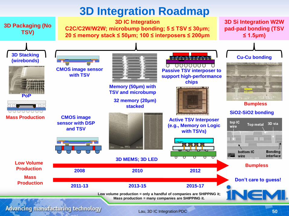
3D Packaging (No
TSV)
3D IC Integration
C2C/C2W/W2W; microbump bonding; 5 ≤ TSV ≤ 30μm;
20 ≤ memory stack ≤ 50μm; 100 ≤ interposers ≤ 200μm
3D Si Integration W2W
pad-pad bonding (TSV
≤ 1.5μm)
3D Stacking
(wirebonds)
PoP
CMOS image sensor
with TSV
Memory (50μm) with
TSV and microbump
Passive TSV interposer to
support high-performance
chips
CMOS image
sensor with DSP
and TSV
32 memory (20μm)
stacked
Active TSV Interposer
(e.g., Memory on Logic
with TSVs)
Mass Production
Low Volume
Production 2008 2010 2012
Don‘t care to guess!Mass
Production2011-13 2013-15 2015-17
Low volume production = only a handful of companies are SHIPPING it;
Mass production = many companies are SHIPPING it.
Cu-Cu bonding
SiO2-SiO2 bonding
3D MEMS; 3D LED
Lau, 3D IC Integration PDC
Bumpless
Bumpless
3D Integration Roadmap
50

What are the Challenges (Opportunities)?
1. Pick and Place of 3D thin chips
2. Pick and place of Bare 3D stacked chips with irregular
shapes
3. Rework processes
4. Heat sink attachment is more difficult
5. Solder joint reliability of large packages
51

Test, Inspection & Measurement TWG
Chair: Mike Reagin,
Delphi
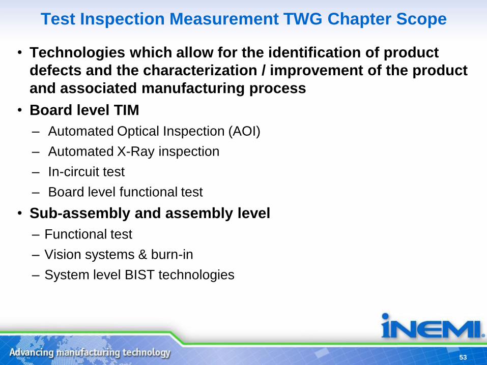
Test Inspection Measurement TWG Chapter Scope
• Technologies which allow for the identification of product
defects and the characterization / improvement of the product
and associated manufacturing process
• Board level TIM
– Automated Optical Inspection (AOI)
– Automated X-Ray inspection
– In-circuit test
– Board level functional test
• Sub-assembly and assembly level
– Functional test
– Vision systems & burn-in
– System level BIST technologies
53
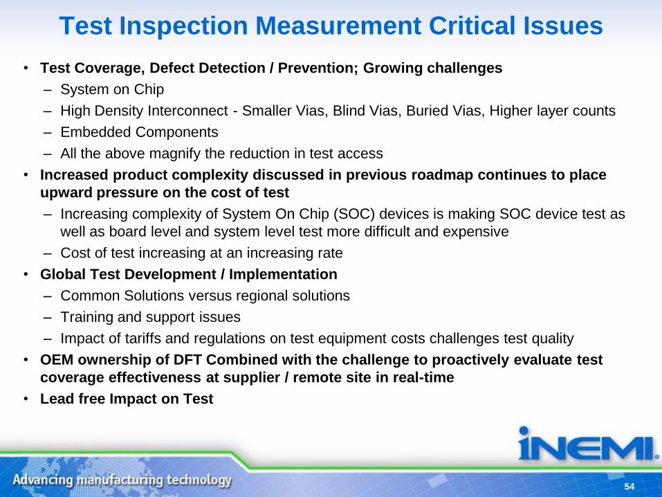
Test Inspection Measurement Critical Issues
• Test Coverage, Defect Detection / Prevention; Growing challenges
– System on Chip
– High Density Interconnect - Smaller Vias, Blind Vias, Buried Vias, Higher layer counts
– Embedded Components
– All the above magnify the reduction in test access
• Increased product complexity discussed in previous roadmap continues to place
upward pressure on the cost of test
– Increasing complexity of System On Chip (SOC) devices is making SOC device test as
well as board level and system level test more difficult and expensive
– Cost of test increasing at an increasing rate
• Global Test Development / Implementation
– Common Solutions versus regional solutions
– Training and support issues
– Impact of tariffs and regulations on test equipment costs challenges test quality
• OEM ownership of DFT Combined with the challenge to proactively evaluate test
coverage effectiveness at supplier / remote site in real-time
• Lead free Impact on Test
54
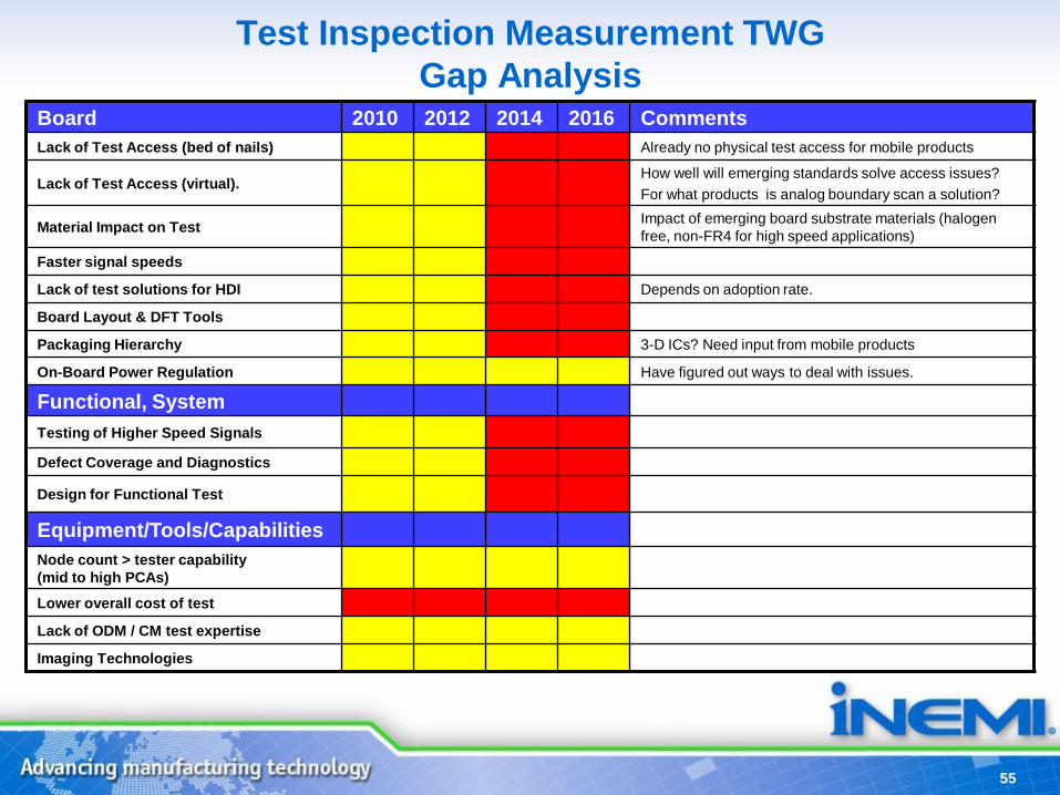
55
Test Inspection Measurement TWG
Gap AnalysisBoard 2010 2012 2014 2016 Comments
Lack of Test Access (bed of nails) Already no physical test access for mobile products
Lack of Test Access (virtual).How well will emerging standards solve access issues?
For what products is analog boundary scan a solution?
Material Impact on TestImpact of emerging board substrate materials (halogen
free, non-FR4 for high speed applications)
Faster signal speeds
Lack of test solutions for HDI Depends on adoption rate.
Board Layout & DFT Tools
Packaging Hierarchy 3-D ICs? Need input from mobile products
On-Board Power Regulation Have figured out ways to deal with issues.
Functional, System
Testing of Higher Speed Signals
Defect Coverage and Diagnostics
Design for Functional Test
Equipment/Tools/Capabilities
Node count > tester capability
(mid to high PCAs)
Lower overall cost of test
Lack of ODM / CM test expertise
Imaging Technologies
Test TWG Summary
• Clearly test challenges are growing to become more severe with time
• Industry collaboration and alignment on strategies to address these gaps is key
• iNEMI projects on BIST standards and portability , Boundary Scan and Board Flexure Standardization are excellent steps
• INEMI projects on component packaging and HFR free laminates will also ultimately drive lower defect rates
• Test strategy/coverage collaboration definition via a face to face Test TWG session is required to address (priorities):
– DFT requirements for 3D packaging
– Specific TIM requirements and strategies to deal with increasing speeds and lowering voltages of products
– Access challenges growing with rapid evolution of HDI
56

Environmentally Conscious
Electronics TWG
Chairs:
Ted Reichert, Intel
(Retired)
Jackie Adams, IBM

ECE TWG Focus
• TWG Focus Topics – Materials
• Ramping restrictions challenge science based evaluation
• Lead and halogen free challenges
• Conflict and rare earth metals
– Energy• Efficiency – harmonized requirements and metrics
• Carbon footprint
– Recycling• Common approach and infrastructure – closer collaboration
• Harmonize patchwork requirements
• Market incentives for recovered materials
– Eco-Design• Better design tools
• Life cycle impact methodologies and database needs
– Sustainability• Our products as an enabler to address climate change
• Water and manufacturing eco-efficiency are emerging areas
58

ECE Summary
• 2011 Issues
– New issues not in previous roadmap that may impact other TWGs
• Rare earth and conflict metals
• Expanding list of restricted materials via global RoHS, REACH
• Carbon footprint
• Cross Cutting Issues
– Highlighted issues that are cross cutting with other TWGs
• Energy efficiency standards and technologies
• Transition to lead free and low halogen
• Additional restricted materials
• Standards for product data management
• Eco-design standards
59

Concluding Thoughts
• New global environmental requirements continue to multiply –faster than industry can effectively respond
• Industry needs to be more proactive in developing solutions that:
– Are based on science and engineering, delivering value to customers
– Are available in advance of new regulations
– Can influence future regulations and stakeholder groups for more sustainable results
• iNEMI and its members are playing a significant role in preparing industry for these future needs
• Sustainability will be a major undertaking for industry as well as society
• Electronic solutions can help to empower people to live a more sustainable lifestyle
60

Summary/Next Steps
Strategic Infrastructural Changes
• The restructuring of the electronics industry over the last decade
from vertically integrated OEMs to a multi-firm supply chain has
resulted in a disparity in R&D needs versus available resources
• Restructuring has created skill gaps at various nodes of supply
chain
• Critical needs for research and development exist in the middle part
of the supply chain (IC assembly services, passive components and
EMS assembly) and yet these are the firms least capable of
providing the resources
• A partial solution has been the development of vertical teams to
develop critical new technology while sharing the costs
• A major gap in this new model is the rapid evaluation of the
reliability and environmental impact of these new technologies by
the supply chain
62
The Next iNEMI Deliverables Are Key:
Addressing the Gaps
• Technology continues to move at a faster rate of change
• Driven in many cases by short life cycle low cost yet high volume
product
• Many of these ―cool new things‖ don‘t port well or quickly to high
reliability markets such as automotive, medical, or high end
networking
• The next key deliverables from iNEMI are the 2011 Technical Plan
(available only to members) and the 2011 Research Priorities
• Effective usage and coordination behind both these documents will
be key to continued industry progress and growth
• Look for them in August of 2011
– The iNEMI TIG‟s and Research Committee are actively working them NOW!
63
RoadmapAvailability

2011 iNEMI Roadmap
• Available to industry beginning today at www.inemi.org as
follows:
– Free for iNEMI members – If interested in joining contact an iNEMI
staff member
– For Non Members:
• $3100 US (complete roadmap CD) International (includes S&H)
• $3000 US (complete roadmap CD) (North America)
• $500 US (per downloaded PDF chapter) - includes executive summary
• Special Rates of $500 US, $600 International for complete RM for
Universities, Research Institutes, and Non Profit Corporations. - $100 Per
chapter for these organizations
• Please contact Chuck Richardson for quantity discount
requests at [email protected]
65

Questions

www.inemi.orgEmail contacts Asia:
Haley [email protected] (Asia)
Chuck Richardson [email protected]
Bill [email protected]

www.inemi.orgEmail contacts Europe/NA:
Grace O’Malley (Europe)[email protected]
Chuck Richardson [email protected]
Bill [email protected]