2009_yield
TRANSCRIPT
882019 2009_Yield
httpslidepdfcomreaderfull2009yield 125
INTERNATIONALTECHNOLOGY ROADMAP
FORSEMICONDUCTORS
2009 EDITION
YIELD ENHANCEMENT
THE ITRS IS DEVISED AND INTENDED FOR TECHNOLOGY ASSESSMENT ONLY AND IS WITHOUT REGARD TO ANYCOMMERCIAL CONSIDERATIONS PERTAINING TO INDIVIDUAL PRODUCTS OR EQUIPMENT
882019 2009_Yield
httpslidepdfcomreaderfull2009yield 225
THE INTERNATIONAL TECHNOLOGY ROADMAP FOR S EMICONDUCTORS 2009
TABLE OF CONTENTS Yield Enhancement 1
Scope1 Difficult Challenges 2
Yield Learning 5 Needed Research 7
Technology Requirements7 Yield Model and Defect Budget 7 Defect Detection and Characterization 9 Wafer Environmental Contamination Control10
Potential Solutions 18 Yield Model and Defect Budget 18 Defect Detection and Characterization 18 Wafer Environmental Contamination Control19
LIST OF FIGURES Figure YE1 General Test Methodology for Ultrapure Water13 Figure YE2 Yield Model and Defect Budget Potential Solutions 18 Figure YE3 Defect Detection and Characterization Potential Solutions 19 Figure YE4 Wafer Environmental and Contamination Control Potential Solutions 20
LIST OF TABLES Table YE1 Definitions for the Different Interface Points 2 Table YE2 Yield Enhancement Difficult Challenges4 Table YE3 Defect Budget Technology Requirement Assumptions 9 Table YE4 Defect Inspection on Pattern Wafer Technology Requirements10 Table YE5 Defect Inspection on Unpatterned Wafers Macro and
Bevel Inspection Technology Requirements 10 Table YE6 Defect Review and Automated Defect Classification Technology Requirements10 Table YE7 Technology Requirements for Wafer Environmental Contamination Control 17
882019 2009_Yield
httpslidepdfcomreaderfull2009yield 325
Yield Enhancement 1
Y IELD E NHANCEMENT S COPE Yield in most industries has been defined as the number of products that can be sold divided by the number of productsthat can be potentially made In the semiconductor industry yield is represented by the functionality and reliability of
integrated circuits produced on the wafer surfaces The scope of this chapter is limited to the yield of front endprocessing The YE chapter does not discuss manufacture line yield assemblypackaging yield and final test yield YieldEnhancement (YE) for manufacturing of integrated devices addresses the improvement from research and developmentyield to mature yield The YE chapter displays the current and future requirements for high yielding manufacturing of DRAM MPU and Flash Furthermore it has the objective to identify the red brick wall for manufacturing and to discusspotential solutions
n-well p-well
n
Via
p
crackshort open
contaminationp+
particle
COP
layer thicknessMetal 1
Metal 2
overlay
p
Interconnects
n+
particle
ESDDamage
Si crystal stacking faults contaminationstress COP
interfaces roughnessstate density charges
n-well p-well
n
Via
p
crackshort open
contaminationp+
particle
COP
layer thicknessMetal 1
Metal 2
overlay
p
Interconnects
n+
particle
ESDDamage
Si crystal stacking faults contaminationstress COP
interfaces roughnessstate density charges
During the manufacturing of integrated circuits yield loss is caused for example by defects faults process variations anddesign During processes as implantation etching deposition planarization cleaning lithography etc failuresresponsible for yield loss are observed Several examples of contaminations and mechanisms responsible for yield loss are
listed in the following a) Airborne Molecular Contamination (AMC) or particles of organic or inorganic matter caused bythe environment or by the tools b) process induced defects as scratches cracks and particles overlay faults and stress c)process variations resulting eg in differing doping profiles or layer thicknesses d) the deviation from design due topattern transfer from the mask to the wafer results in deviations and variations of layout and critical dimensions and e)diffusion of atoms through layers and in the semiconductor bulk material
The determination of defects and yield and an appropriate yield to defect correlation are essential for yield enhancementThis correlation is of major importance because not all defects change device properties or cause failure of devices orintegrated circuits Therefore the yield enhancement chapter addresses not only the identification of tolerablecontamination limits for processes and media but also the tolerable budgets for particulate contamination of tools Thespecification of tools for defect detection and classification of defects for root cause analysis addresses the technologyrequirements for detection and characterization of faults and failures
The YE chapter has three focus topics lsquoYield Model and Defect Budgetrsquo lsquoDefect Detection and Characterizationrsquo andlsquoWafer Environment Contamination Controlrsquo These three topics crosscut front end process technology interconnectprocesses lithography metrology design process integration test and facility infrastructures Yield learning is discussedwithout identification of the red brick wall for manufacturing or potential solutions
Yield Model and Defect Budget mdashYield model has been developed for the purpose of predicting the yield of products andproviding information how to improve them Historically yield has been limited by extra and missing materials generatedin the fabrication environment and showed good correlation with defect density of the wafer Defect budget have had arole of breaking down the targeted yield into the targeted control limit of every process module in the fabrication lineHowever current most serious yield issue has been changed from said physical defect to insufficient compensation or
THE INTERNATIONAL TECHNOLOGY ROADMAP FOR S EMICONDUCTORS 2009
882019 2009_Yield
httpslidepdfcomreaderfull2009yield 425
2 Yield Enhancement
countermeasure for manufacturability at the design stage General consensus or agreements of modeling abovementionedissue have not been established yet
Defect Detection and Characterization mdashPhysical device dimensions and corresponding defect dimensions continueshrinking posing new challenges to detection and tolerable contamination The wafer edges were identified to showsignificant impact on yield as well as process variations and design Development of defect detection defect review andclassification technologies showing highest sensitivity at high throughput is crucial for cost efficient manufacturingAutomated intelligent analysis and reduction algorithms which correlate facility design process test and work-in-
progress data will have to be developed to enhance root cause analysis and therefore enable rapid yield learningWafer Environment Contamination Control mdashOrder-of-magnitude improvements in process critical fluid and gas impuritylevels are not considered to be necessary in the foreseeable future New materials and their precursors however introducechallenges that require continuous study Clarification of potential contamination from point-of-supply to point-of-process will define control systems necessary for delivered purity There are several locations in the pathway from theoriginal delivery package ie the Point of Supply (POS) of a liquid or gas to the location where that material contacts thewafer ie the Point of Process (POP) for ascertaining purity This has led to a considerable amount of confusion andambiguity in discussing the quality of process fluids including the data found in Table YE7 Table YE1 summarizes themajor fluid handling andor measurement nodes found along the typical systems supplying process fluid This table is aneffort to create a common language for the discussion of attributes and requirements at these different node pointsFurther information regarding pathway nodes can be found in the supplementary materials and references such as theSemiconductor Equipment and Materials International (SEMI) Standards
Table YE1 Definitions for the Different Interface Points POS POD POC POE POU PO
Delivery Point of GasChemical
Supplier
Outlet of Central Facility System
Submain or VMBVMP
Take off Valve
Entry to Equipment or Sub Equipment
Entry to the ProcessChamber Contact with Wafer
Interfaces SEMI Standards Focus Area
ITRS Factory Integration Facilities Group Focus Area
ITRS Factory Integration Equipment Group Focus Area
ITRS Front End Processes
Lithography Interconnect TWG
Focus Area
Ultrapurewater Raw water Outlet of final filtration
in UPW plant
Outlet of submain takeoff valve
Inlet of wet bench orsubequipment
Inlet of wet bench bathspray nozzle orconnection point topiping which is also usedfor other chemicals
Wafer in production
Processchemicals
Chemical
drumtotebulk supply
Outlet of final filtration
of chemical distributionunit
Outlet of VMBvalve
Inlet of wet bench orintermediate tank
Inlet of wet bench bath orspray nozzle Wafer in production
Specialtygases
Gas cylinder orbulk specialty gassystems
Outlet of final filtrationof gas cabinet
Outlet of VMBvalve Inlet of equipment Inlet of chamber (outlet of
MFC) Wafer in production
Bulk gasesBulk gasdelivered on siteor gas generator
Outlet of finalfiltrationpurification
Outlet of submain takeoff valve orVMB valve
Inlet of equipment subequipment
Inlet of chamber (outlet of MFC) Wafer in production
Cleanroomand AMC Outside air Outlet of make-up air
handling unit
Outlet of filtersin cleanroomceiling
Inlet to mini-environment or subequipment for AMCoutlet of the tool filterfor particles
Gasair in vicinity towafersubstrate
Wafersubstrate inproduction (AMC SMC)
PODmdashpoint of delivery POCmdashpoint of connection POEmdashpoint of entry POUmdashpoint of use VMBmdash valve manifold boxVMPmdash valve manifold post UPWmdashultra pure water MFCmdashmass flow controller AMCmdashairborne molecular contaminationSMCmdashsurface molecular contamination
D IFFICULT C HALLENGES The difficult challenges for the Yield Enhancement chapter are summarized in Table YE2 Currently the most importantkey challenge will be the detection of multiple killer defects and the signal-to-noise ratio It is a challenge to detectmultiple killer defects and to differentiate them simultaneously at high capture rates low cost of ownership and highthrough put Furthermore it is a dare to identify but yield relevant defects under a vast amount of nuisance and falsedefects As a challenge with second priority the requirement for 3D inspection was identified This necessitates forinspection tools the capability to inspect high aspect ratios but also to detect non-visuals such as voids embedded defects
THE INTERNATIONAL TECHNOLOGY ROADMAP FOR S EMICONDUCTORS 200 9
882019 2009_Yield
httpslidepdfcomreaderfull2009yield 525
Yield Enhancement 3
and sub-surface defects is crucial The demand for high-speed and cost-effective inspection tools remains The need forhigh-speed and cost-effective 3D inspection tools becomes crucial as the importance of 3D defect types increases E-beaminspection seems not to be the solution for all those tasks any more
Other topics challenging the Yield Enhancement community are prioritized as follows in the near term
bull Process Stability vs Absolute Contamination Level
bull Wafer Edge and Bevel Monitoring and Contamination Control
In 2009 a new long term key challenge was identified This is the introduction of 450 mm wafers which is expected toimpact the defect detection and characterization but as well defect budgets and yield models due to the large surface of the substrate The introduction of 450 mm wafers requires a new generation of inspection tools The cost of ownership isimpacted by throughput and tool cost It will be difficult to maintain the throughput of inspection tools at the 450 mmwafer size Therefore the tool costs are crucial 450 mm handling for inspection has the risk of large substrate flexibilitybut also coordinate accuracy required for defect review Due to the large surface a huge amount of inspection data will beobtained Improvement of data quality and reduction of the amount of data will be important Defect budgets and yieldmodels are impacted by the unknown defect densities on the large substrates Data test structures and methods areneeded for correlating process fluid contamination types and levels to yield and to determine the required control limitsThe issues for this challenge are to define the relative importance of different contaminants to wafer yield a standard testfor yieldparametric effect and a maximum process variation (control limits) The fundamental challenge is to understandthe correlation between impurity concentration in key process steps and device yield reliability and performance Thiscorrelation will determine whether further increases in contamination limits are truly required The challenge increases incomplexity as the range of process materials widens and selection of the most sensitive processes for study will berequired for meaningful progress
Furthermore in the long term the following key challenges are identified
bull Non-Visual Defects and Process Variations
bull In - line Defect Characterization and Analysis
bull Development of model-based design-manufacturing interface
THE INTERNATIONAL TECHNOLOGY ROADMAP FOR S EMICONDUCTORS 2009
882019 2009_Yield
httpslidepdfcomreaderfull2009yield 625
4 Yield Enhancement
Table YE2 Yield Enhancement Difficult Challenges Difficult Challenges ge 16 nm Summary of Issues
Existing techniques trade-off throughput for sensitivity but at expected defect levels boththroughput and sensitivity are necessary for statistical validity
Reduction of inspection costs and increase of throughput is crucial in view of CoO Detection of line edge roughness due to process variation Electrical and physical failure analysis for killer defects at high capture rate high
throughput and high precision
Reduction of background noise from detection units and samples to improve the sensitivityof systems Improvement of signal to noise ratio to delineate defect from process variation
Detection of Multiple Killer Defects Signal to Noise Ratio- Detection of multiple killer defects and their simultaneousdifferentiation at high capture rates low cost of ownershipand high throughput It is a challenge to find small but
yield relevant defects under a vast amount of nuisance and false defects
Where does process variation stop and defect start Detection of non visible defects eg voids embedded defects and sub surface defects in the
structuresThe demand for high-speed and cost-effective inspection is crucial
Large number of contacts and vias per wafer E-beam inspection seems not to be the solution for all those tasks any more
3D Inspection ndash For inspection tools the capability toinspect high aspect ratios but also to detect non-visuals
such as voids embedded defects and sub-surface defects iscrucial The need for high-speed and cost-effective 3Dinspection tools becomes crucial as the importance of 3Ddefect types increases Sensitivity of the inspection tool to process variation and definition of maximum process
variation (control limits)Methodology for employment and correlation of fluidgas types to yield of a standard test
structureproduct Relative importance of different contaminants to wafer yield
Process Stability vs Absolute Contamination Level ndash Including the Correlation to Yield Test structures methodsand data are needed for correlating defects caused bywafer environment and handling with yield This requiresdetermination of control limits for gases chemicals air
precursors ultrapure water and substrate surfacecleanliness
Define a standard test for yieldparametric effect
Wafer Edge and Bevel Monitoring and ContaminationControl ndash Defects and process problems around wafer edgeand wafer bevel are identified to cause yield problems
Currently the monitoring and contamination control methods require intensivedevelopment
Difficult Challenges lt 16 nm Summary of IssuesSystematic Mechanism Limited Yield (SMLY) resulting from unrecognized models hidden in
the chip should be efficiently identified and tackled through logic diagnosis capabilitydesigned into products and systematically incorporated in the test flow It is required tomanage the above models at both the design and manufacturing stage Potential issues canarise due to
a) Accommodation of different Automatic Test Pattern Generation (ATPG) flowsb) Automatic Test Equipment (ATE) architecture which might lead to significant test time
increase when logging the number of vectors necessary for the logic diagnosis to convergec) Logic diagnosis runs time per died) Statistical methodology to analyze results of logic diagnosis for denoising influence of
random defects and building a layout-dependent systematic yield model
Non-Visual Defects and Process Variations ndash Increasing yield loss due to non-visual defects and process variationsrequires new approaches in methodologies diagnosticsand control This includes the correlation of systematic
yield loss and layout attributes The irregularity of featuresin logic areas makes them very sensitive to systematic yield loss mechanisms such as patterning process variationsacross the lithographic process window
Test pattern generation has to take into account process versus layout marginalities(hotspots) which might cause systematic yield loss and has to improve their coverage
Data volume + quality strong increase of data volume due to miniaturizationThe probe for sampling should show minimum impact as surface damage or destruction
from SEM image resolution It will be recommended to supply information on chemical state and bonding especially of
organicsSmall volume technique adapted to the scales of technology generations
In - line Defect Characterization and Analysis ndash Based onthe need to work on smaller defect sizes and featurecharacterization alternatives to optical systems and
Energy Dispersive X-ray Spectroscopy systems arerequired for high throughput in-line characterization and analysis for defects smaller than feature sizes The datavolume to be analyzed is drastically increasing thereforedemanding for new methods for data interpretation and toensure quality [1]
Capability to distinguish between the particle and the substrate signal
A lot of models should be operated at the design stage For example Optical ProximityCorrection Well Proximity Stress Proximity CMP and so on
The Amount of models seems to be rapidly increasing Not only accuracy of models but also optimization of trade-off between models might be
requested
Development of model-based design-manufacturing interface mdash Due to Optical Proximity Correction (OPC)and the high complexity of integration the models must comprehend greater parametric sensitivities ultra-thin filmintegrity impact of circuit design greater transistor
packing etc Development of test structures for new technology generationsThe cost of ownership is impacted by throughput and tool cost It will be difficult to
maintain the throughput of inspection tools at the 450 mm wafer size Therefore the tool costsare crucial
450 mm handling for inspection has the risk of large substrate flexibility but also coordinateaccuracy required for defect review
Due the large surface a huge amount of inspection data will be obtained Improvement of data quality and reduction of the amount of data will be important
The introduction of 450 mm wafers is expected to impactthe defect detection and characterization but as well defectbudgets and yield models due to the large surface of thesubstrate The introduction of 450 mm wafers requires anew generation of inspection tools
Defect budgets and yield models are impacted by the unknown defect densities on the large substrates
THE INTERNATIONAL TECHNOLOGY ROADMAP FOR S EMICONDUCTORS 200 9
882019 2009_Yield
httpslidepdfcomreaderfull2009yield 725
Yield Enhancement 5
Y IELD L EARNING
I NTRODUCTION Yield learning is defined as the collection and application of process and wafer knowledge to improve device yieldthrough the identification and resolution of systematic and random manufacturing events Currently yield learning is notdescribed by technology requirements and potential solutions
The semiconductor industry operates in an environment of exponentially decaying product prices which put
semiconductor manufacturers under time-to-market pressure Profitability is derived from an early and successful yieldramp The sooner a semiconductor manufacturer generates high yield the earlier the manufacturer ramps to volumeproduction and the more profitable the semiconductor manufacturerrsquos integrated circuit venture is likely to be Improvingthe systematic component of yield which frequently constrains yield in the early stages of manufacturing can enhanceprofitability by enabling production at a point in time when chip prices are very high Yield learning in the early stages of manufacturing may thus differ significantly from yield learning in the later stages of manufacturing Beside this anytransition from one technology generation to the next is accompanied by a decrease in initial yield Along with atechnology generation change for example new materials or litho processes have to be introduced These changes haveto be implemented in parallel with new technology generations Monitoring capabilities inspection metrology toproperly cover the issues of latest technology generations cause enormous expenses and require concentrated research anddevelopment
The key requirements for achieving highly sophisticated yield ramps include the detection of ever-shrinking yield-detracting defects of interest timely identification of root causes with growing data volume chip complexity processcomplexity and improving the yield learning rate per each cycle of learning With increasing process complexity andlonger cycle times tools and methods are needed to increase the number of yield learning cycles for each technologygeneration Also with continuous move to smaller features and longer processes larger wafers and new materialsnumerous tools and methods are required to understand the entire yield detracting interactions
D ATA M ANAGEMENT AND ADVANCED P ROCESS C ONTROL AND F AULT D ETECTION AND C LASSIFICATION (FDC) Yield Management in a factory is going to be more closely coupled to data management The rapid identification of defect and fault sources through integrated data management is the essence of rapid yield learning Learning must proceedat an accelerated rate to maintain the yield ramp from introduction to maturity within the expected timeline despite thegrowth in circuit complexity and the larger amount of data acquired on a given wafer lot As integrated circuit fabricationprocesses continue to increase in complexity it has been determined that data collection retention and retrieval ratesincrease exponentially This is getting significant importance now and in the future In advanced manufacturing any data
generated could potentially hold the key to understanding and solving a yield issue that is identified at wafer sort andneeds to be recorded in an accessible way for the yield engineers if required Accessing the raw data in such a way as togenerate meaningful correlations and results is going to be a critical requirement for manufacturing Data storage andconsequently the user interfaces to access this data cannot be handled as an afterthought if these factories are to besuccessful during the start upHow the data from all generating sources of the factory is collected stored compiled and accessed is going to be crucialIn the face of this increased complexity strategies and software methods for integrated data management have beenidentified as critical for maintaining productivity Integrated device manufacturing must comprehend integrated circuitdesign visible and non-visual defects parametric data and electrical test information to recognize process trends andexcursions to facilitate the rapid identification of yield detracting mechanisms Once identified the integrated devicemanufacturing system must source the product issue back to the point of occurrence The point of occurrence is defined tobe a process tool design test or process integration issue that resulted in the defect parametric problem or electricalfault Integrated device manufacturing will require a merging of the various data sources that are maintained throughout
the fabrication environment This confluence of data will be accomplished by merging the physical and virtual data fromcurrently independent databases The availability of multiple data sources and the evolution of automated analysistechniques such as Automatic Defect Classification (ADC) and Spatial Signature Analysis (SSA) can provide amechanism to convert basic defect parametric and electrical test data into useful process informationImplemented Advanced Process Control (APC) and Fault Detection and Classification (FDC) solutions will be of increasing importance However these control solutions will require tremendous data transport and data processingsystems to support a full-scale implementation Managing this which must all be done in real time to benefit the factoryis a monumental undertaking Maintaining standards and open access systems allowing the best internal and externalsolutions to work together is a must
THE INTERNATIONAL TECHNOLOGY ROADMAP FOR S EMICONDUCTORS 2009
882019 2009_Yield
httpslidepdfcomreaderfull2009yield 825
6 Yield Enhancement
Down stream or rather offline analysis of all the factoriesrsquo data will also require new approaches in addition to theexisting ones to fully grasp all information that can be correlated to yield The greatest challenge to a comprehensive datamanagement system required for yield learning is the ability to deal with and integrate data streams that are continuousperiodic sporadic and interval-based so they can all be linked through some common coupling system or user interfaceand be resolved by engineers Keeping data aligned down to the wafer level or possibly to the die level requiresautomated data matching techniques It is also critical to have all data sources open and accessible by multiple userinterfaces in order to maximize the effectiveness of yield engineering resources in finding problems The best-of-breeddata systems going forward will allow internal as well as multiple third party software solutions and Graphical UserInterfaces (GUIs) to access the raw data formats giving engineers the greatest flexibility in identifying and solving yieldlimiting issues Barriers such as these must be eliminated
The current practice in Data Management System (DMS) technology is to maintain several independent databases thatcan be accessed by different engineering groups for yield analysis This data is used for base-line analysis excursioncontrol trend identification process design and yield prediction
A fundamental impediment to efficient integrated device manufacturing is a lack of standards on which to base systemcommunication data formats and a common software interface between data repositories The creation of useablestandards is also needed to facilitate automation methods Current engineering analysis techniques are highly manual andexploratory by nature The ability to automate the retrieval of data from a variety of database sources such as based onstatistical process control charts and other system cues will be required to efficiently reduce these data sources to process-related information in a timely manner To close the loop on defect and fault sourcing capabilities methods must beestablished for integrating workflow information (WIP) such as data determined with the DMS particularly in
commercial DMS systems This will be important when addressing issues of advanced process and tool control beyondsimple tool shutdown eg lot and wafer re-direction tool prognostics and health assessment
DMS systems today are limited in their ability to incorporate time based data generated from in situ process sensors toolhealth and tool log data Methods for recording time based data that can be correlated with lot and wafer-based data areneeded
Even though there is a wide variety of manufacturing data accessible through the DMS system today yield predictiontools and methods continue to be limited to a small number of experts The ability to provide these analysis techniques toa broader engineering group will result in the rapid prioritization of defect generating mechanisms and a fasterengineering response to the most important of these issues
F OUNDRY S PECIFIC Y IELD LEARNING Yield learning in a foundry differs substantially from yield learning in a fabrication facility that produces a few high-
volume products The high-volume producer will be constrained by batch yield in the early stages of manufacturing Lineyield will be the limiting factor once batch yield is high and volume production has begun By contrast a foundry mayintroduce a plethora of low-volume products into a relatively mature process on a routine basis On occasion one lot of wafers may provide a lifetime inventory of a particular design which sells into a very short market window A few chipsof the design must exit the fabrication facility by a specific date Due to this it is more important to get a initially defectfree design of the integrated circuit to get a initially flawless masks and to obtain immediately a rapid cycle time throughthe line combined with a high line yield instead of a high batch yield
D EFECTS The various types of defects are described in the following
Visible Defects mdashTools are needed to detect review classify analyze and source continuously shrinking visible defects
Non-visual Defects mdashDefects that cause electrical failure but do not leave behind a physical remnant that can beaffordably detected with todayrsquos detection techniques are called non-visual defects As circuit design becomes morecomplex more circuit failures will be caused by defects that leave no detectable physical remnant Some of these failureswill be systematic and parametric in nature such as cross-wafer and cross-chip variations in resistance or capacitance ortiming others will be random and non-parametric such as stress caused dislocations and localized crystallinebondingdefects The rapid sourcing of the latter (non-parametric random and non-visual defects) will become increasinglychallenging Techniques need to be developed that rapidly isolate failures and partition them into those caused by visibledefects non-visual defects and parametric issues
Parametric Defects mdashAs minimum feature size decreases so does the systematic mechanism limited yield (SMLY or Y s)A major contributor to the Y s component of yield is parametric variation within a wafer and wafer-to-wafer Parametric
THE INTERNATIONAL TECHNOLOGY ROADMAP FOR S EMICONDUCTORS 200 9
882019 2009_Yield
httpslidepdfcomreaderfull2009yield 925
Yield Enhancement 7
defects have traditionally been referred to as lsquonon-visual defectsrsquo However parametric defects require separation fromthe ldquonon-visual defectsrdquo for rapid sourcing
Electrical Faults mdashAs the number of steps the number of transistors and the circuit density increases and the criticaldefect size decreases an increasing number of defects are only seen as electrical faults This includes faults caused byspot defects and faults caused by parametric process disturbances In order to perform defect sourcing the electrical faultmust be isolated (localized) within the chip The complexity of this task is roughly proportional to the pattern number of awafer times the number of process steps forming a defect sourcing complexity factor In order to maintain the defect
sourcing time the time to isolate (localize) the electrical fault within the chip must not grow despite the increasingcomplexity Moreover the soft failures caused by sporadic cross-chip timing variation will require innovative newapproaches to identify the root causes since these type of failures reside between a hard spot defect failure and consistentsystematic failure issue
N EEDED R ESEARCH
The technology requirements and potential solutions described in 2007 call for continued cooperation between allstakeholders For example tool defect data is needed from semiconductor manufacturers and equipment manufacturers tospecify design processes and the required equipment A challenge for the future will be the detection of smallest defects athigh throughput Currently there are no solutions known This situation is also observed for control of critical dimensionswith respect to the expected scaling down progress As e-beam inspection is too slow the development of scatterometryor other optical methodologies seems more promising Furthermore the future transition of metrology tools to inspectiontools has to be performed as the yield issues get more and more complex related to the small feature sizes at atomic scale2007 the importance of flatness control of surfaces was recognized during cross technical working group discussions Theproblem is solved for bare wafer inspection but not for pattern wafer inspection Enormous RampD efforts are required toobtain solutions for the above mentioned red brick wall within the next years
In order to maintain manufacturing costs while improving yield contamination control must focus on impact at the pointof process Innovative ideas such as local removal of undesirable contamination from a re-usable process gas or fluidmust be examined For new thin-film materials understanding of purity requirements for deposition chemicals is needed
Performance analysis indicates replacements for SEMEDX that are also activated by e-beam illumination Auger-electron spectroscopy can be used in the short-term to augment and replace SEMEDX analysis because Auger-electrongeneration can only escape a target particle from a depth of approximately 3 nm or less This property of Auger electronsspecifically avoids a large sampling volume
In the next two to three years SEMEDX can be further improved by more versatile e-beam acceleration control and X-ray detection methods More sensitive detection methods include micro-calorimetry and WDS
For elemental and bonding analysis of particles that are 60 nm diameter and below Scanning Transmission ElectronMicroscopy (STEM) Electron Energy Loss Spectroscopy (EELS) holds good promise for performance in the next 3 to 5years STEMEELS has the capabilities to simultaneously capture elemental analysis while imaging the atomic structureof the constituents of a particle Automated sample preparation must be improved and accelerated to achieve timely ultra-thin samples of 50-100 nm thickness Aberrations of incoming and transmitted e-beams must be mitigated to enable theidentification of constituent elements and compounds by the sizing of these constituents from images alone
T ECHNOLOGY R EQUIREMENTS
Y IELD M ODEL AND D EFECT B UDGET
The overall die yield of an IC process can be described as a product of material-defect limited yield (Y M) systematicmechanism limited yield (SMLY - Y S) and random-defect limited yield (Y R) (see Equation 1) Y M separates yielddegradation caused by defects embedded in a starting material from Y S andor Y R during wafer fabrication Furtherinformation about Y M is described in FEP chapter In most cases Y M is negligible Y S requires problem specific modelingand general formula to describe Y S is currently unknown A negative binomial yield model is adopted to calculate Y R inYE chapter A is the area of the device D 0 is the electrical fault density and α is the cluster factor Parameters required tocalculate D 0 are defined in Table YE3
THE INTERNATIONAL TECHNOLOGY ROADMAP FOR S EMICONDUCTORS 2009
882019 2009_Yield
httpslidepdfcomreaderfull2009yield 1025
8 Yield Enhancement
α
α ⎟⎟
⎟
⎟
⎠
⎞
⎜⎜
⎜
⎜
⎝
⎛
+==
01
1
ADY Y Y Y Y Y S M RS M Die
(1)
2
11
1
⎟
⎟
⎠
⎞
⎜
⎜
⎝
⎛ times=
minusminus
minus
n
nn
nnn
S S
F
F PWP PWP (2)
The previously published tables for defect budgets (YE4 and YE5 in ITRS 2007) were deleted because of the lack of accuracy supported by surveys among semiconductor manufacturers Although based on results of old studies (19971999 and 2000) of Particles per Wafer Pass (PWP) levels at SEMATECH member companies they are still useful as areference for investigating defect reduction target toward new technology generation or discussing difference betweenseveral specific processes In the Equation 2 PWP is the particles per wafer pass defect density per square meter F is theaverage faults per mask level (determined by the random electrical fault density (D 0) divided by number of masks at agiven technology generation) S is the minimum critical defect size and n refers to the technology generation
Table YE3 states the yield and the product maturity assumptions that were used in calculating electrical fault densityvalues and PWP defect budget target values for MPUs DRAMsFlashs respectively These assumptions for the most partare as defined in the 2009 Overall Roadmap Technology Characteristics (ORTC) Cluster parameter value of 2 permits
slight non-uniformity of fault distribution on wafers The electrical fault density that is used to calculate faults per mask level is based on only the periphery (logicdecoder) area of the chip This periphery area can be calculated from cell arrayarea at production defined in Table ORTC-2A Since there is no redundancy in the periphery this portion of the chip mustconsistently achieve the 895 random-defect limited yield It is assumed that the core (array) area of the DRAMFlashcan implement redundancy to attain the overall yield target of 85
Besides continuous improvement in tool cleanliness there are at least three other major challenges that must be addressedgoing forward in order to achieve acceptable yields
1 The issues of particles and defects which are located not only at the front surface of a wafer but also at waferbeveledge portion and backside surface needs to be addressed
2 With Systematic Mechanisms Limited Yield (SMLY) dominating the rate of yield learning a concerted effort isrequired to understand model and eliminate SMLY detractors
3 New methodology including APC should be evaluated the possibility of becoming a new variationdefect source
THE INTERNATIONAL TECHNOLOGY ROADMAP FOR S EMICONDUCTORS 200 9
882019 2009_Yield
httpslidepdfcomreaderfull2009yield 1125
Yield Enhancement 9
Table YE3 Defect Budget Technology Requirement Assumptions Product MPU DRAM Flash
Yield Ramp Phase Volume Production
Volume Production
Volume Production
Y OVERALL 75 85 85
Y RANDOM 83 8950 8950
Y SYSTEMATIC 90 95 95Y MATERIAL gt99 gt99 gt99
Chip Size 140mm2
93mm2
144
Cluster Parameter 2 2 2
D EFECT D ETECTION AND C HARACTERIZATION
The ability to detect in-line yield-limiting defects on specific process layers is the primary requirement of a defectdetection technology The extension of this ability to the diverse throughput requirements of various phases of production-process research and development yield ramp and volume production mdash broadens the applicability of thetechnology and creates extremely complex solutions that must be fast and sensitive This is becoming more critical asfabrication facilities begin to run different products in multiple stages of process maturity through the same defect
detection tools to extract maximum returns from extensive capital investment in such toolsThe respective capabilities must be ready for use by the integrated device manufacturers just in time for each phase of theprocess cycle Tools that meet the requirements for process research and development are typically required well inadvance of the planned introduction of a technology generation Tools that can accelerate yield ramp must be availableseveral months before production begins Finally the ability to monitor excursions at a technology generation is neededwhen the product hits high yield levels
Technology requirements are presented by three tables covering the needs for a) patterned wafer - and e-beam inspectionb) unpatterned wafer inspection macro and bevel inspection and defect review and c) Defect Review and AutomatedDefect Classification (ADC) The complexity of processes and integration schemes for manufacturing of integrateddevices requires intense defect inspection for process and tool monitoring Unpatterned wafer inspection is extensivelyused for tool qualification Both defect inspections use subsequent defect review for root cause analysis posingchallenging requirements to the accuracy of defect coordinates Furthermore the cleanliness of inspection tools is of increasing importance Due to the observed impact of defects on wafer bevel and edge on yield backside and bevel waferinspection needs a defect review possibility in order to be used to the full extent High aspect ratio inspection defined asthe detection of defects occurring deep within structures having depth to width ratios greater than 3 is inspected on e-beam tools which find their application also in detection of small defects
One of the major challenges is to get to the defect of interest Therefore the signal-to-noise ratio is an important criterionfor all inspection tools The more nuisance defects are captured the less valuable the results are as defects of interestmight not be recognized even after intense review Furthermore an efficient separation of DOI from noise will enable anincreased throughput of the subsequent review
The inspection of bevel apex and wafer edge on the top and bottom on multilayer product wafers is nowadays possiblewith a variety of tools Anyway the variety of process problems having their origin in those areas of the wafer requiresdefect classification which is challenging for any inspection tool Important criteria besides coverage of all areassensitivity and speed are the ADC and the optical review capability on the tool as well as a standard result file allowingSEM review
The technology requirements for defect detection on unpatterned wafers depend on the film and substrate Detection of defects on the backside of wafers without introducing any contamination or physical contact on the front side is desirableThe wafer backside inspection requirements are based on the Lithography chapter technology requirements table and alsoask for specification of tool cleanliness of the inspection tools themselves this was introduced
Several other defect modes need to be addressed by detection tools A better understanding of non-visible killers defectsthat can not be detected with conventional optical technologies is emerging with the increased usage of e-beam basedtechnologies Most of these defects tend to be sub-surface and possess a significant dimension in the longitudinaldirection or z-axis A clear definition is not yet available for the minimum size of such defects that must be detected
THE INTERNATIONAL TECHNOLOGY ROADMAP FOR S EMICONDUCTORS 2009
882019 2009_Yield
httpslidepdfcomreaderfull2009yield 1225
10 Yield Enhancement
Many have electrically significant impact to device performance and can occur in both the front end of the process(process steps prior to contact oxide deposition) and the back end of the process Macro defects impacting large areas of the wafer should not be overlooked because of the urgency to address the sub-micron detection sensitivities stipulatedbelow Scan speeds for macro inspection should be continuously improved matching the wafer throughput (plus overheadof the inspection) of the lithography and possibly CMP systems at every technology generation
Semiconductor manufacturers balance the costs and benefits of automated inspection by inspecting with sufficientfrequency to enable rapid yield learning and avoid substantial risk of yield loss The cost of the investment fab space
occupied and the throughput of defect detection tools are major contributors to their cost of ownership (CoC) CurrentlyCoO forces many semiconductor manufacturers to deploy such tools in a sparse sampling mode Statistically optimizedsampling algorithms are needed to maximize the yield learning resulting from inspection tool usage In order to maintainacceptable CoO in the future the throughput the sensitivity as well as the use of adaptive recipe options of theseinspection tools must be increased If future tools operate at increased sensitivity with decreased throughput therebyincreasing their CoO semiconductor manufacturers will have to adopt even sparser sampling plans thereby increasingtheir risk of yield loss and slowing their yield learning rates
The requirements for sensitivity in Table YE4 YE5 and YE6 have been stipulated on the basis of detecting accuratelysized PolyStyrene Latex (PSL) spheres that are deposited on test and calibration wafers However new tools are mostlyevaluated on their capability to detect real defects that occurred during process development that were captured usinghigh-resolution microscopy Such defects include particles pits pattern flaws surface roughness and scratches There isan urgent need for the development of a defect standard wafer that will enable objectively evaluating new and existingdefect detection tools to accommodate the growing palette of defect types on various layers
Table YE4 Defect Inspection on Pattern Wafer Technology Requirements
Table YE5 Defect Inspection on Unpatterned Wafers Macro and Bevel Inspection Technology Requirements
Table YE6 Defect Review and Automated Defect Classification Technology Requirements
W AFER E NVIRONMENTAL C ONTAMINATION C ONTROL
Wafer environmental contamination control requirements are categorized by manufacturing materials or environment asshown in Table YE7
Wafer environment control mdashThe wafer environment control includes the ambient space around the wafer at all timeswhether the wafers are open to the cleanroom air or stored in PODsFOUPs As the list of ambient contaminants to becontrolled broadens so must measurement capabilities Affordable accurate repeatable real time sensors for non-particulate contamination are becoming increasingly necessary The use of inert environments to transport and storewafers is expected to increase with process sensitivities Pre-gate pre-contact clean salicidation exposed copper andreticle exposure are cited as processes that first require this capability In addition using inert environments offers theopportunity to reduce the introduction of moisture into vacuum load-lock tools thereby decreasing contamination andload-lock pump-down times While closed carrier purging systems exist and are evolving tool environments that mayneed to become inert such as wet sink end-stations present a challenge As wafer isolation technologies evolve designand material selection of carriers and enclosures will be critical for performance in isolating the wafers from the ambientand in not contributing contaminants themselves In addition the materials and designs must not promote cross-contamination between processes Seal technology low-outgassing and non-absorbing materials development are key toeffective wafer and reticle isolation deployment
Airborne molecular contamination mdashOutgassing from materials of construction in the cleanroom wafer processingequipment and wafer environmental enclosures as well as fugitive emissions from chemicals used in wafer processing arethe two main sources of AMC Oxygen and water vapor as well as low concentration atmospheric contaminants (egCO) can also be considered as part of the AMC burden Acid vapors in the air have been linked with the release of boronfrom HEPA filters and the impact of amines on Deep UltraViolet (DUV) photoresists are well known examples of AMCaffecting wafer processing The impact of AMC on wafer processing can only be expected to become more deleterious asdevice dimensions decrease There is a need for better AMC monitoring instrumentation in the cleanroom to measureAMC at the part per trillion level (by volume) Surface Acoustic Wave (SAW) devices and Atmospheric Pressure IonizedMass Spectroscopy (APIMS) have been used to measure low level AMC but low cost routine monitoring may be
THE INTERNATIONAL TECHNOLOGY ROADMAP FOR S EMICONDUCTORS 200 9
882019 2009_Yield
httpslidepdfcomreaderfull2009yield 1325
Yield Enhancement 11
required as devices approach molecular dimensions see also AMC monitoring programs Hydrocarbon films of only afew monolayers may lead to loss of process control especially for front-end processes Although numerous studiesrelated to AMC outgassing from the materials of construction of environmental enclosures and FOUPs have beenperformed to guide material selection for these enclosures the need for nitrogen purging of wafer environment enclosuresis being investigated for critical process steps Not all process steps will be impacted by AMC For example futurelithography systems will require vacuum processing and are not expected to impose new AMC control requirements inthe cleanroom environment The potential for AMC to impact new processes should be considered in all processintegration studies A detailed definition of critical impurities is provided in AMC definitions
Temperature and humidity specifications have been added to Table YE7 this year for the most critical applications eglithography for several reasons
1) The strictest requirements are driven by the lithography process which is protected by an environmentalchamber The specifications in the Table YE7 reflect the inlet condition to each individual environmentalchamber Here especially the maximum variation over time is important which the environmental chamber
must be able to compensate At the POP lower specifications down to plusmn 003 deg K are maintained
2) But also in the coaterdeveloper track temperature and humidity specifications must be guaranteed to maintainstable conditions for the resist
3) The temperature variation is also important for the stepper itself since minor temperature variations can resultdue to different thermal extension coefficients in misalignments between the stepper foundationwafer stage andthe lens column Steppers need up to a week to stabilize after a temperature change
4) Another critical requirement is driven by metrology equipment which depend either on laser beams (the airdensity depend on temperature and humidity) and by measurements where misalignments are important
The temperature and humidity stability over different locations within critical areas is less important Also in other areastemperature and humidity variations shall be controlled to less strict limits since it may have an impact on the surface(native oxide formation) or alignments Some companies choose not to have different specifications for critical and non-critical areas to allow flexibility in the cleanroom use as well as simplify the temperature and humidity control and theassociated segregation
These specifications are variational specifications and set points can be chosen in a wide range A recent benchmarkingstudy between fabs has shown values between 195 and 24degC for temperature and values between 35 and 48 for therelative humidity There are different drivers for that The temperature set point is normally chosen based on comfortlevel and climatic conditions and the resulting energy consumption The set point for relative humidity takes intoconsideration higher electrostatic charges at lower humidity and higher corrosionnative oxide formation at higher relativehumidity Capacity of AMC filters also depends on the humidity
Another process area with temperaturehumidity control as well as AMC control requirements is the location of thelithography excimer lasers if they are installed in the subfab and not in the main cleanroom
Process critical materials mdashAdditional experimental investigation is required to support our understanding of impurityspecifications in novel materials such as Cu plating solutions CMP slurries or chemical vapor deposition (CVD)precursors to highlow- κ dielectrics and other thin film materials For many years the critical particle size concept wasused to judge whether particles will have an impact on yield or not This concept has to be rethought since particles do notimpact the process yield alone by their physical size but also by their chemical composition The allowable particleconcentration thereby depend also on product parameters such as cell size and have therefore been aligned with theparticle concentration on the surface as derived by the FEP surface preparation group calculation model
Ultrapure water mdashUPW is generally considered to be 182 Meg Ω-cm resistivity at 25degC low ppt in metals less than50 ppt in inorganic anions and ammonia less than 02 ppb in organic anions and below 1 PPB total oxidizable carbon(TOC) and silica (dissolved and colloidal) Particle levels are reduced using the best available ultrafiltration technologyBacteria are present on surfaces and to a lesser degree in the bulk fluid and controlled to very low levels typicallylt1 colony forming unit (cfu)L in the bulk fluid The 2007 Roadmap values presented in Table YE7 represent typicalUPW quality currently in use to manufacture the most advanced semiconductor devices and have been validated bybenchmark surveys More stringent criteria beyond 2007 are only projected where there is evidence that manufacturingprocess requirements demand improvements UPW is generally the cleanest fluid available in the manufacturing processAs such there is not much data to suggest that it is has a significant negative impact on process yields For this reason theUPW Roadmap is relatively stable over time The UPW group is evaluating Gibbs Free Energy deposition models to
THE INTERNATIONAL TECHNOLOGY ROADMAP FOR S EMICONDUCTORS 2009
882019 2009_Yield
httpslidepdfcomreaderfull2009yield 1425
12 Yield Enhancement
indicate the potential for critical elements to deposit on the wafer under various process conditions A discussion of theUPW requirements can be found in the UPW supplemental material onlineThe UPW section of Table YE7 considers some parameters as process variables rather than contaminants It is clear thatthe stability of the wafer environment can be as important as the level of contaminants present for some parameters Somesemiconductor manufactures now treat Dissolved Oxygen (DO) in this way while others still consider it a contaminantStability of temperature and pressure continue to be important the former being critically important for immersionlithography
Contaminant quality levels in UPW must be viewed in the context of where that quality is required and where it is to bemeasured Points of measurement are referred to as the POD POE and POU The POD is just after the last treatment stepof the UPW system the POE is at the tool connection point and the POU is in the tool Refer to Table YE1 for detaileddescription of sample locations The 2007 Roadmap defines UPW quality at the POE in Table YE7 UPW quality canchange between these three locations especially between the POE and POU and requires particular attention to maintainquality throughout In addition sampling techniques are critical to ensure accurate analytical results As UPWspecifications shift from the POE to the POU sampling methods will become more difficult and costly Most benchmark data has been collected at POD or POE and is the basis for parameters in Table YE7 A benchmark of POE and POUvalues was conducted in 2007 however results were not received in time for publishing These results will be consideredfor the 2008 update Where contaminant levels have been extended to POU this has been done based on engineering
judgment assuming the semiconductor processing tool is well designed and operated with regard to maintaining fluidpurity in accordance with applicable SEMI standardsOzonated UPW is not addressed in this Roadmap as it is considered a dilute process chemistry that is generally applied at
the process tool At the time of printing immersion lithography posed no special requirements for UPW other thanpossible degasification and additional closer temperature control which would be done at the process toolImmersion Lithography processes which use UPW as the lens fluid is very sensitive to temperature and hazing of the lensTool manufacturers are interested in minimizing all potential sources of organics Accelerated hazing tests are beingconducted to see if the organic species known and thought to be in UPW can contribute to lens hazing Results were notavailable at the time of printing but will be considered in the 2008 updateUPW recyclemdash To promote resource optimization UPW use efficiency improvements are typically required Costeffective technologies including treatment and analytical methods are needed to ensure UPW quality is maintained asmore water is recycled back through the system A well-implemented recycle program has been shown to improve finalwater quality by using a ldquocleanerrdquo stream for the feed in addition to providing other benefits Further information andrequirements can be found in the Environmental Safety and Health chapterUPW measurement methodologiesmdash General test methodologies for monitoring contaminants in UPW are indicated in theFigure YE1 below Over the past few years the ITRS UPW team has benchmarked many advanced UPW systems todetermine water quality The 2007 benchmark effort includes Non Volatile Residue Monitoring and particles by SEMwith a novel sample collection method Past benchmark efforts have identified the inadequacy of some measurementmethodologies to quantify contaminants in UPW The following analytical methods are not sensitive to present levels of contamination in UPW resistivity total oxidizable carbon inorganic anions and organic ions as well as some organicspecies Speciation of organics has been limited by these methods Sensitivity of the following methods is presentlyadequate viable bacteria dissolved gasses and metals While particle measurement is generally not adequately sensitiveat the critical dimension it may be technically sound to extrapolate particle size and concentration data to the criticaldimension Benchmarking has shown this size distribution to be unique to a particular UPW system andor measurementtechnique Each user of the Roadmap is advised to determine a particle distribution for their fab empiricallyBenchmarking has indicated a log log distribution relationship with slopes from -1 to -5 A more complete treatment of UPW concerns is covered in the supplemental material of this chapter online where also a conversion tool can be found
THE INTERNATIONAL TECHNOLOGY ROADMAP FOR S EMICONDUCTORS 200 9
882019 2009_Yield
httpslidepdfcomreaderfull2009yield 1525
Yield Enhancement 13
Parameter Measured (PODPOC) Test Method
Resistivity Online Electric cell Viable bacteria Lab Incubation TOC Online ConductivityCO 2 Inorganic anions and NH 4 + Lab Ion chromatography Organic ions Lab Ion chromatography
Other organics Lab Various eg ES TOF ICP-MS Reactive silica Online or lab Colorimetric Dissolved N 2 Online Electric cell Total silica Lab ICP-MS or GFAAS Particle monitoring Online Light scatter Particle count Lab SEMmdashcapture filter at various pore sizes Cations anions metals Lab Ion chromatography ICP-MS
Dissolved O 2 Online Electric cell ES TOFmdashElectro spray time of flight ICP-MSmdashinductively coupled plasma mass spectrometryGFAASmdashgraphite furnace atomic absorption spectrometry
Figure YE1 General Test Methodology for Ultrapure Water
THE INTERNATIONAL TECHNOLOGY ROADMAP FOR S EMICONDUCTORS 2009
882019 2009_Yield
httpslidepdfcomreaderfull2009yield 1625
14 Yield Enhancement
UPW and liquid chemicals particle measurementmdash Problem Definition and Goals The sensitivity limit of particlecounters for UPW and liquid chemicals has not kept pace with decreases in the critical particle size (the size of particleswhich are thought to be detrimental to wafer yield) Although this concept needs to be discussed again since particles notonly impact yield because of their physical dimensions but even more by the chemical composition eg as spot Fecontamination the fact remains the same It is important to measure even smaller particles than we can do todayMeasurements of these nanoparticles are made difficult by the low scattering efficiency of them Low particleconcentrations and small sample volumes of current particle monitors can result in large sample-to-sample variabilityMore sensitive particle measurement methodology with adequate measurement statistics is needed to meet projectedpurity goals
The Sensitivity Problem As of 2007 the highest sensitivity particles counter commercially available for UPW is 005microns and for liquid chemicals is 0065 microns Experiments have shown that small particles may even depositpreferentially [M Knotter] and therefore the impact is increased even further Past improvements in particle countersensitivity for UPW have been accomplished by increases in laser power While improvements in sensitivity for liquidchemical particle counters are viable further sensitivity improvements for UPW using this approach are unlikely due tothe significant cost implications In addition high-cost solutions do not necessarily guarantee a production-worthymetrology tool High initial expense coupled with increased cost of ownership impact the viability of higher sensitivityinstruments To estimate the concentration of smaller particles currently an extrapolation assumes a 1d 3 relationshipbetween particle counts and particle size in liquids The further away the particle size of interest gets from actualmeasurement capabilities the higher the potential for error-error being defined as the difference in the projected value tothe true value Therefore it is still important for the industry to develop a more sensitive method that can measure particle
concentrations at greater sensitivity to validate the particle count versus particle size relationship so that the relationshipcan continue to be reliably used
The Measurement Precision Problem Statistical process control is increasingly being used to monitor the consistency of process parameters Process variation of fluid purity can be as critical to wafer yield as the absolute purity of the fluidsTherefore it is important that measurement methods detect sufficient number of events to ensure confidence in measuredparticle concentrations Development of other statistically significant particle counting methods or a higher samplevolume particle counter is needed to improve confidence in reported particle counts The sample volume (volume of fluidmeasured) will determine the number of particle counts that are detected during the sample interval Refer toSupplemental Information link Particle monitoring for more detail
Although the gasliquid chemical section of Table YE7 shows an essentially flat purity trend there is likelihood thatspecific process steps may require higher purity Yield improvements may be achieved more by reducing variations inpurity than by reduction of average contamination levels There is therefore a need for improved statistical processcontrol of contamination levels during manufacturing and delivery of these process materials
Overview for gases and liquid chemicalsmdash The recommended contaminant values for gases and chemicals in Table YE7represent typical gasliquid chemical quality requirements at the point of entry to the process tool (POE) for the moredemanding manufacturing processes in the roadmap In many applications the requirements for the contaminants in thesegases andor liquid chemicals may be relaxed as dictated by the specific process requirements On the other hand somemanufacturers have claimed benefits from lower contaminant levels Considering that a given process can be runsuccessfully within a ldquowindowrdquo defined by a range of material purity and also by ranges in other parameters (purgingtime etc) it follows that in practice trade-offs exist between imposed purity requirements process throughput etcPushing a process to the upper limit of its ldquopurity windowrdquo may require significant investment of time and effort inoptimizing other parameters and the economics of pursuing that effort will depend on the environment It may also bethat benefits attributed to low contaminant levels are more attributable to the reduction in contaminant variations achievedwith high-purity process gases and chemicals This topic is addressed in more detail below regarding the push for theadoption of statistical process control SPC for specifying process fluid purity
There are three primary sources of process environment contamination One is the impurities in the process materials assupplied The second is the delivery system or the process itself The third is decomposition which may be causedthermally or by reaction with adventitious contaminants eg moisture These contamination sources are found throughoutthe pathway from the delivered gas or chemical to the wafer surface Table YE1 describes the several interfacial points of process materials with equipment found along these paths and associates them with the various TWGs within the ITRSand other organizations such as SEMI that focuses on them This helps to clarify the relationship of these organizationswith the WECC while also removing ambiguity about the definition of various points along the process path
While purity measurements at the Point of Process POP (that is in the processing chamber itself) would provide themost direct correlation between gas or liquid quality and process performance these measurements are often very difficult
THE INTERNATIONAL TECHNOLOGY ROADMAP FOR S EMICONDUCTORS 200 9
882019 2009_Yield
httpslidepdfcomreaderfull2009yield 1725
Yield Enhancement 15
to obtain with the exception of certain fluid properties in wafer immersion baths Examples include both particulategeneration during plasma processes and wafer outgassing The latter is the most important source of water vaporcontamination in many processes often obscuring moisture contributions from the process fluid Measurements at thePOU provide the most direct information of the quality of process fluids going directly into the process chamber butthese are also not available for many of the common processes
Because of these difficulties the values in Table YE7 are intended to represent those at the Point of Entry POE definedas the inlet to the process tool as described in Table YE1 There are sufficient measurement data on bulk gases and
aqueous fluids to provide guidance with regard to POE impurity levels for many applications although measurements onthese fluids are often performed at the POS POD or POC For these materials which are relatively unreactive anddelivered in large volume the extrapolation to POE is generally very reasonable In the case of Specialty Gases and otherreactive process fluids such extrapolation is more delicate because delivered volumes are smaller increasing sensitivityto contamination effects and degradation in the distribution system related to materials of construction atmosphericcontamination thermal degradation etc is more likely These factors are minimized with normal best construction andoperations practices and therefore the best guidance available is often regarding POS specification and to a lesser extentPOD or POC measurements which are interpreted as equivalent to POE In summary while the intention is torecommend POE purity levels for all gases and liquids in practice the supporting data has more often been collected atPOS POD or POC
The targeted levels can be reached either by bulk delivery of a fluid with requisite purity or through use of a localpurificationfiltration Care should be taken at a minimum to maintain the quality of the gas coming from the sourceensuring that contamination is not added downstream of the POS as may occur due to particle generation at components
moisture out gassing byproduct generation due to incompatible materials etc Particle filtration as close to the POU aspossible is generally advisable for gases For the most critical applications a local purifier may be used to enhance orensure ultimate purity at the POU In those cases the prevailing approach is to seek POC levels that are adequate for theprocess and to view the purifier as ldquoinsurancerdquo The challenge to the purifier is minimal and long purifier lifetimes cannormally be expected
Specific purity challenges will be discussed below but generally there is little objective evidence to suggest that thepurity levels listed in Table YE7 are not suitable for multiple generations of semiconductor manufacturing Yieldimprovements are expected to be achieved by reducing variations in purity Statistical process control (SPC) on incomingmaterials will reduce variation at the POS Inconsistencies at the POU may remain due to variations in downstreamcontributions eg when the flow in a distribution system is decreased moisture contamination due to out gassing tendsto increase Elimination of these variations may require purification at the appropriate point (eg POU purificationPOUP)
The major bulk gases are listed separately in Table YE7 The 2007 roadmap had indicated an increase in purityrequirements post 45 nm This type of improvement might be anticipated based upon historical trends as design rulestightened but there is again little objective evidence to support the need for improvements across the range of bulk gasesInformal poling of several large semiconductor manufacturing organizations suggests that an increase above currentpurity requirements for the majority of bulk gases is not necessary to meet post 45 nm design rule manufacturing Forvery special applications where extraordinarily higher purities are critical special purity grades or additional purificationwill be required As exemplified above downstream POUP might also be utilized as an additional means of removingvariability in POS gases Therefore Table YE7 has been modified from 2005 to remove many of the step improvementsscheduled for future manufacturing nodes except where specific information has been identified to justify the change
The situation is similar for many of the Specialty Gases although several additional categories of applications have beenadded to better identify needs for specific processes eg etch deposition doping and laser applications Like the Bulk gases the values in Table YE7 have been left at current levels unless an objective justification for increased purity can beidentified Although changes to the current table YE7 values for gases are small the introduction of so many new
materials and the process innovations required to meet future design rules eg atomic layer deposition will require closemonitoring More details with regard to bulk and specialty gases are provided in the Gas supplemental documents
The 2005 roadmap identified the growing need for statistical process control for process gases and liquids Severalcompanies have begun requesting materials with specifications related to the statistical control of variability of thematerials but there are no standards accepted across the industry that define the SPC process Currently there is a Semisponsored task force composed of representatives from the end user and supplier communities that is creating a commonset of characteristics for defining ldquoin controlrdquo specifications for gases and liquids
THE INTERNATIONAL TECHNOLOGY ROADMAP FOR S EMICONDUCTORS 2009
882019 2009_Yield
httpslidepdfcomreaderfull2009yield 1825
16 Yield Enhancement
The promise of providing ldquoin controlrdquo process fluids is anticipated to improve process yields by either minimizing theoverall variability of the manufacturing process or in simply reducing the likelihood of a process crash resulting fromlarge variations in material quality that would still nominally have met a more standard specification
An informal survey of several large semiconductor manufacturing companies on their implementation of statisticalprocess control requirements for their bulk and specialty gas purchases indicates that SPC processes are already beingapplied to many of the materials utilized in manufacturing or will be shortly However the criteria that form the basis of ldquoin controlrdquo varies substantially Survey responses suggest that customer expectation is that the application of process
control for the preparation of POS materials will improve their semiconductor manufacturing process stability and arecritical for high yield manufacturing Initial implementation will likely focus on specialty gases that exhibit the greatestpotential for causing semiconductor process variability eg anhydrous HCl but will be used on new and existingproducts for both memory and microprocessors
Liquid chemicals mdashTable YE7 summarizes the purity requirements for liquid chemicals delivered to process tools Pre-diffusion cleaning requirements drive the most aggressive impurity levels Liquid particle level targets are shown tobecome purer each technology generation These target values are derived from the purity requirements on a wafer ascalculated by the FEP surface preparation group assuming a linear relationship between the concentration in the liquidand on the wafer Particle counters currently are capable of measuring only to 65 nm for liquid chemicals By assuming aparticle size distribution it should be possible to infer particle concentrations to smaller particle sizes but this will beinfluenced by the level of filtration utilized Another measurement challenge for several chemicals is the differentiationbetween particles and bubbles which is currently not possible
The ability to accurately analyze organic anion and cation contamination in process chemicals is becoming more criticalto successful wafer processing In the supplementary materials an ion table and a mixing calculation is provided whichshows for which chemicals which ions are important and in which chemicals they could actually occurhave beenobserved With the increased use of CMP and plating chemicals there must be a better understanding of purityrequirements for the delivered chemicals Table YE7 contains information only for very few CVDALD precursors Thevariety of layers and the respective contaminants is enormous Therefore a link to the precursor table is provided in thesupplementary materials online The precursor table provides information by application as to which precursors arepotential candidates at different technology generations and the nature of contamination that can be expected A majorchallenge is the development of accelerated yield learning for critical processes that introduce new precursors that willonly be used for one or two generations
Bulkspecialty gases mdashThere were only a few changes to the bulk gas purity requirements The measurement of organicrefractory components at lt01 ppb is a detect ability challenge for both nitrogen and helium used in lithographyapplications The roadmap indicates these areas as orange from 2007 to 2010 because this is at the limit of detection for
current analytical methodsIn addition changes were made to better delineate the need to control Ar as an impurity The N 2 specification waschanged to eliminate Ar as a critical impurity although it was left in the O 2 specification Even so the 50 ppbv limitgiven in 2005 was raised to an Ar limit of lt1000 ppbv The ongoing requirement in O 2 derives from the potential foruncontrolled Ar impurities to impact plasma etching processes although typical Ar specifications for O 2 used for etchingis more consistent with the lt1000 ppbv level
For some processes such as advanced lithography very small quantities of ldquohigh molecular weighthigh boiling pointrdquo(eg C 6-C 30) hydrocarbons are detrimental because of increased adherence to the exposed surfaces and potential forphotochemical degradation to leave non-volatile residues on lenses masks mirrors etc However any organics evenones with retention times less than C 6 are considered detrimental if they can result in refractory deposits For the samereason other potential impurities such as siloxanes or organophosphates can also be very detrimental in extremely smallquantities In order to detect such species with ultimate sensitivity it is necessary to directly detect the relevant speciesand calibrate the analyzer with the appropriate standard The methods used are analogous to those for AMC such as TDgas chromatography (GC)mass spectroscopy (MS) (TD = thermal desorption) or TD GCFID or ion mobilityspectroscopy (IMS) Even these approaches may miss some heavier hydrocarbons andor polar species that tend to remainin the column or emerge as very broad peaks For methods using adsorbent traps it is very important to determine the trapefficiency Using APIMS to provide real time measurement of individual hydrocarbons is possible in principle butcalibration is difficult because larger hydrocarbons are collisionally dissociated in the ionization process
A compromise approach that has gained some acceptance is to use TD GCMS and sum all peaks corresponding to C6and higher The instrument is usually calibrated with a multi-component standard and results are reported ldquohexadecanerdquo
THE INTERNATIONAL TECHNOLOGY ROADMAP FOR S EMICONDUCTORS 200 9
882019 2009_Yield
httpslidepdfcomreaderfull2009yield 1925
Yield Enhancement 17
While the quantization provided by this method is approximate and some species may be overlooked it does at leastemphasize the heavier hydrocarbons while providing a straightforward calibration
Applications for both O 2 and H 2 generally tolerate higher levels of N 2 contamination than other contaminants and thetable reflects this observation Requirements for critical clean dry air (CDA) lithography purge gases and supercriticalCO 2 supply are included Whereas critical CDA may not always be conveniently or cheaply available there is notechnological barrier to its production Analytical methods are usually the same as used for airborne molecularcontamination in clean room air such as bubbling through ultra pure water (for metals sulfates amines etc) or trapping
on an adsorbent trap for organics In each case the sampler concentrates impurities so that requisite sensitivities areachieved when the sample is introduced to the analyzer (ICP-MS or ion chromatography for aqueous samples GC-MS fordesorption of organics) Such methods are time consuming by nature and direct methods would be preferred if availableHowever there is no apparent pressing need for real-time analysis For SO 2 there are convenient on line methods egUV fluorescence
For specialty gases contaminant values in etchants dopants and deposition gases have been expanded in Table YE7 toreflect the increase number of different materials in use and to better delineate the processes they are used for Particulatecontamination is omitted since online monitoring of particle concentrations is not commonly practiced and the efficacy of POU particle filters is well established Whereas there is evidence that the most demanding applications such as lowtemperature epi and its cleaning gases will continue to benefit from improvements in purity as deposition temperaturesare lowered this is expected to be reflected in wider use of the best available purity rather than substantial improvementsof those levels
Tighter control over the variation in purity in both bulk and specialty gases is anticipated to be more important thanimprovement in absolute purity levels However the often more chemically reactive specialty gases present a moreformidal challenge for maintaining of POS purity levels throughout the delivery to the point of process Selected specialtygases eg HCl are also expected to be among the first targeted for statistical process control at the POS
Novel materials mdashMore detailed consideration of the impurity levels found in the growing number of novel materials usedin processing will be increasingly important Requisite purity levels for critical materials such as novel metal oxidesCMP slurries lowhigh k dielectric materials precursor materials (such as CVD and electroplating solutions) for barrierand conductor metals (such as Cu Ta) have not been widely studied and many of these materials have not been called outin Table YE7 An early attempt to start to catalogue and characterize the properties of the thin film precursors utilized insemiconductor processing is found in the supplementary material for this chapter (provide link)
Deposition precursors for thin film materials are often sensitive to moisture air and high temperatures Control over thedelivery process from the POS to the reaction chamber is critical to high yielding performance The use of very highpurity carrier and purge gases in these systems are often required to prevent decomposition that can contribute detrimentalmolecular and particulate impurities Traditionally bulk purifiers were used in the bulk gas delivery systems to removeparticles and other homogeneous chemical contaminations like oxygen or moisture present in the supply gases Howeverwith the development and commercial availability of point-of-use (POU) purifiers there is a strong interest from endusers to utilize point-of-use (POU) purifiers particularly for specialty gases needed for critical process steps with verycritical level of contamination control These point-of-use purifiers (POU) are highly effective to remove chemicalcontaminants to extreme low level (~ ppt) easy to use easy to replace with low cost-of-ownership The capability of placing those point-of-use (POU) purifiers very close to inlet of process chamber assures least travel path (lesscontamination) for process gases after chemical purification and filtration
Novel measurement techniques and impact studies are needed to ensure that these materials are produced with theimpurity specifications that meet technology requirements Additional detail on the variety of thin film precursors underconsideration can be found in Liquid Chemicals section of Table YE7 and the supplementary precursor table
Table YE7 Technology Requirements for Wafer Environmental Contamination Control
THE INTERNATIONAL TECHNOLOGY ROADMAP FOR S EMICONDUCTORS 2009
882019 2009_Yield
httpslidepdfcomreaderfull2009yield 2025
18 Yield Enhancement
P OTENTIAL S OLUTIONS
Y IELD M ODEL AND D EFECT B UDGET
Very small particles will request study of thermophoresis andor Van Der Waals force to understand behavior in the nearfuture Currently yield society does not have enough experience about particles between molecular and optically visible
particles Research into precise yield model assisted by TCAD is becoming important because SMLY issues tend torestrict yield ramping rate and attainment level Ever increasing NRE also requests understanding of SMLY and itseffective implementation to product Parametric limited yield issues including line edge roughness and design to processmismatch also tend to limit yield This will require research into new characterization devices and statistical methods toorganize measured data Figure YE2 illustrates a few potential solutions that may help address the technologyrequirements for future yield modeling
First Year of IC Production 2009 2010 2011 2012 2013 2014 2015 2016 2017 2018 2019 2020 2021 2022 2023 2024
Yield ModelSMLY model generationSMLY model based DFMScaling Proces complexity
Defect BudgetingTest structures to clasify and quantifyandor non-visual defects
This legend indicates the time during which research development and qualificationpre-production should be taking place for the solutionResearch Required Development Underway Qualification Pre-Production Continuous Improvement
Figure YE2 Yield Model and Defect Budget Potential Solutions
D EFECT D ETECTION AND C HARACTERIZATION
For pattern wafer inspection the requirements the next years will be to overcome issues of detection of the defects withinthe nuisance signal This is correlated to the issue to obtain high sensitivity at high throughput Major breakthroughs arerequired to achieve the required throughputs at roadmap sensitivities for yield ramp and volume production Waferedgebevel inspection will require methods to filter and to classify defects Really challenging is the review capability atthe wafer edge The review is the enabler for defect to yield correlation and therefore essential for high yieldingproduction The research and development should focus on methods to filter out the defects of interest automatically Thehigh aspect ratio inspection is still requiring for high yield at high throughput due to the high cost of ownership of theinspection tools This requires also a good separation of the defect signals from the noise The introduction of 450 mmsubstrates will start research activities in the area data quality and reduction of data amount Also impacted and a need forresearch is the coordinate accuracy of inspection and subsequent review As mentioned before this is essential for theyield improvement especially required during ramp up Due to the doubled surface area of the new substrates a researchtopic for the next years will be the throughput simulation and according improvement
THE INTERNATIONAL TECHNOLOGY ROADMAP FOR S EMICONDUCTORS 200 9
882019 2009_Yield
httpslidepdfcomreaderfull2009yield 2125
Yield Enhancement 19
First Year of IC Production 2009 2010 2011 2012 2013 2014 2015 2016 2017 2018 2019 2020 2021 2022 2023 2024
Pattern Wafer InspectionHigh sensitivity at high throughputHigh signal to noise ratio
Wafer EdgeBevel InspectionMethod to filter and classify defectsReview capability
High Aspect Ratio InspectionHigh sensitivity at high throughputHigh signal to noise ratio
450 mm inspectiondata quality and reduction of data amountcoordiante accuracythroughput
This legend indicates the time during which research development and qualificationpre-production should be taking place for the solutionResearch Required Development Underway Qualification Pre-Production Continuous Improvement
Figure YE3 Defect Detection and Characterization Potential Solutions
W AFER E NVIRONMENTAL C ONTAMINATION C ONTROL
Process Equipment mdashDefect reduction in process equipment remains paramount to achieving defect density goalsSolutions and technology developments are expected to provide major enhancement capabilities in the next 15 years andcontinue to enable cost-effective high volume manufacturing for device dimensions below 90 nm Refer to Figure YE4Equipment defect targets are primarily based on horizontal scaling Vertical faults particularly as they apply to the gatestack metallic and other non-visual contaminants and parametric sensitivities need to be understood New cleaningchemistries in situ chamber monitoring materials development and other techniques including improved techniques of parts cleaning can help maintain chamber cleanliness run-to-run and dramatically reduce the frequency of chamber wetcleans These developments will also act to increase equipment utilization Reduced backside wafer contamination controlmust drive both measurement technology and fundamental changes in equipment Metalparticle cross contaminationfrom backside to next wafer front-side hot spotsdepth of focus in lithography and punch through on electrostatic chucks
are all examples of issues that must be addressed in future tools Particle avoidance techniques (o-ring material selectiongas flowtemperature management wafer chuck optimization) will continue to play a key role in meeting defect densitiesIt is believed that a more fundamental understanding of reactor contamination formation transport and deposition will berequired to enhance current equipment and process design and aid in the placement and interpretation of data from in situ sensors These fundamental physical chemical and plasma reactor contamination models must be employed In situprocess control will become increasingly important to reduce process-induced defects and to minimize requirements forpost-measurements Intelligent process control at a tool requires a fundamental understanding of how parameters impactdevice performance Open tool control systems that allow both users and equipment suppliers to easily integrate newsensor and new control software will be necessary to enable intelligent process control
Process critical materials mdashFigure YE4 illustrates the set of potential solutions for prevention and elimination of defectsFurther studies into device impact are necessary to validate any need for increased purities System concerns such ascorrosion potential may lead process concerns in seeking higher purities
In order to accelerate yield enhancement for processes that incorporate new materials it is very desirable thatdevelopment studies include purity data as much as is practical Studies of new materials (eg for gate dielectrics) areinitially concerned with basic process performance and later with integration issues During those stages of developmentcontamination is a relatively minor concern However if no information is collected later yield enhancement effortsproceed with inadequate technical basis Collecting and reporting both environmental and material contamination datawhenever practical will lead to long-term benefits
UPW mdashUPW systems meeting specifications do not appear to be large defect drivers for current device geometries Basedon this the Roadmap does not predict that significant changes are required for future geometries As a Roadmap priorityspecific defect mechanisms related to UPW are required to drive significant changes The current focus is to understand
THE INTERNATIONAL TECHNOLOGY ROADMAP FOR S EMICONDUCTORS 2009
882019 2009_Yield
httpslidepdfcomreaderfull2009yield 2225
20 Yield Enhancement
the impact of the tool upon water quality specifically particles bacteria and dissolved gasses as well as to identifyspecies that are suspected to be in UPW but are below the detection limit of available measurement methods Improvedmeasurement methodologies are required for organics and organic ions to specify low-level contaminants in UPWRecycling and reclaiming initiatives must drive improvements in rapid online analytical technology especially detectionof organics to ensure that POU-recycled UPW is equal or better than single-pass water
Chemicals mdashFigure YE4 shows various technological areas that may be required to enhance and measure the purity of delivered chemicals to the wafer manufacturing process
Wafer environment control mdashAs the list of ambient contaminants to be controlled broadens so must measurementcapabilities Affordable accurate repeatable real time sensors for non-particulate contamination are becomingincreasingly necessary The use of inert environments to transport and store wafers is expected to increase with processsensitivities Pre-gate and pre-contact clean and salicidation are cited as processes to first require this capability Inaddition using inert environments offers the opportunity to reduce the introduction of moisture into vacuum load-lock tools thereby decreasing contamination and load-lock pump-down times While closed carrier purging systems exist andare evolving tool environments that may need to become inert such as wet sink end-stations present a challenge Aswafer isolation technologies evolve design and material selection of carriers and enclosures will be critical forperformance in isolating the wafers from the ambient and in not contributing contaminants themselves In addition thematerials and designs must not promote cross-contamination between processes Seal technology low outgassing andnon-absorbing materials development are key to effective wafer isolation deployment
First Year of IC Production 2009 2010 2011 2012 2013 2014 2015 2016 2017 2018 2019 2020 2021 2022 2023 2024
GENERAL
Fluid purity impact on device yield performance
Contaminant based process control
AIRAMC
On-line monitor for AMC contaminants - TotalRefractory Compounds
On-line monitor for AMC contaminants - Bases -Improvements of amines detection
On-line monitor for AMC contaminants - AcidsMA beyond corrosion monitoring
On-line monitor for AMC contaminants -Condensable high molecular weight organics
Reduced cost of ownership for AMC control
Development of emergency response proceduresand measures for fugitive emissions
Verification for AMC limits relative to processexcursions or yield events
Figure YE4 Wafer Environmental and Contamination Control Potential Solutions
THE INTERNATIONAL TECHNOLOGY ROADMAP FOR S EMICONDUCTORS 200 9
882019 2009_Yield
httpslidepdfcomreaderfull2009yield 2325
Yield Enhancement 21
First Year of IC Production 2009 2010 2011 2012 2013 2014 2015 2016 2017 2018 2019 2020 2021 2022 2023 2024
ULTRAPURE WATER
Metal samplingdetection capability
Metal deposition Understanding
Tool blanketing to preclude dissolved O2 increase
Particle counting techniques for directmeasurement of smaller particles
Colloidal Silica as a surrogate measure ofparticles in UPW
Organics speciation and analytical capabilities toprovide information about organic molecularweight and chemical species class
Yield impacts of various organic species
TOC analysis for chemical family and molecularweight identification
Figure YE4 Wafer Environmental and Contamination Control Potential Solutions (continued)
THE INTERNATIONAL TECHNOLOGY ROADMAP FOR S EMICONDUCTORS 2009
882019 2009_Yield
httpslidepdfcomreaderfull2009yield 2425
22 Yield Enhancement
First Year of IC Production 2009 2010 2011 2012 2013 2014 2015 2016 2017 2018 2019 2020 2021 2022 2023 2024
CHEMICALS
Development of sub 65 nm particle counter
Filtration 002004 microm with high flux (1 gpm05psi101cP)
Filtration sub 002 microm with higher flux
Reduced pressure fluctuations by improved BCDsystem performance and by better pressure andflow control
Improved blend accuracy taking into accountincoming chemical concentration changes (closedloop control capability)
Improved metrology for concentrationmeasurements
Improved flow capacity for piping components
Improved connection technology (reduceleakages)
Higher purity resins (metals organics anionscations surface smoothness permeability)
Particle characterization to identify source ofcontamination
Anion amp cation measurement in processchemicals eg cleaning chemicals
Organic measurement (TOC and speciation) inprocess chemicals eg H2O2 IPA
Contaminant characterization in CMP slurrieseg zeta potential large particle size
On-line contaminant and constituentmeasurement in plating chemicals eg coppersulfate organic additives
Figure YE4 Wafer Environmental and Contamination Control Potential Solutions (continued)
THE INTERNATIONAL TECHNOLOGY ROADMAP FOR S EMICONDUCTORS 200 9
882019 2009_Yield
httpslidepdfcomreaderfull2009yield 2525
Yield Enhancement 23
First Year of IC Production 2009 2010 2011 2012 2013 2014 2015 2016 2017 2018 2019 2020 2021 2022 2023 2024
PRECURSORS
Particle measurement for precursors
Other analyzer techniques for precursors(precursor specific contaminants seesupplementary table)
GASESDevelopment of statistically process c ontrolled(SPC) based specifications for critical specialtygases
Bulk gas purity requirements specifically ofcarrier and purge gases for moisture sensitivematerials
Blending accuracy for low concentrations ofdopant mixtures
Figure YE4 Wafer Environmental and Contamination Control Potential Solutions (continued)

882019 2009_Yield
httpslidepdfcomreaderfull2009yield 1725
Yield Enhancement 15
to obtain with the exception of certain fluid properties in wafer immersion baths Examples include both particulategeneration during plasma processes and wafer outgassing The latter is the most important source of water vaporcontamination in many processes often obscuring moisture contributions from the process fluid Measurements at thePOU provide the most direct information of the quality of process fluids going directly into the process chamber butthese are also not available for many of the common processes
Because of these difficulties the values in Table YE7 are intended to represent those at the Point of Entry POE definedas the inlet to the process tool as described in Table YE1 There are sufficient measurement data on bulk gases and
aqueous fluids to provide guidance with regard to POE impurity levels for many applications although measurements onthese fluids are often performed at the POS POD or POC For these materials which are relatively unreactive anddelivered in large volume the extrapolation to POE is generally very reasonable In the case of Specialty Gases and otherreactive process fluids such extrapolation is more delicate because delivered volumes are smaller increasing sensitivityto contamination effects and degradation in the distribution system related to materials of construction atmosphericcontamination thermal degradation etc is more likely These factors are minimized with normal best construction andoperations practices and therefore the best guidance available is often regarding POS specification and to a lesser extentPOD or POC measurements which are interpreted as equivalent to POE In summary while the intention is torecommend POE purity levels for all gases and liquids in practice the supporting data has more often been collected atPOS POD or POC
The targeted levels can be reached either by bulk delivery of a fluid with requisite purity or through use of a localpurificationfiltration Care should be taken at a minimum to maintain the quality of the gas coming from the sourceensuring that contamination is not added downstream of the POS as may occur due to particle generation at components
moisture out gassing byproduct generation due to incompatible materials etc Particle filtration as close to the POU aspossible is generally advisable for gases For the most critical applications a local purifier may be used to enhance orensure ultimate purity at the POU In those cases the prevailing approach is to seek POC levels that are adequate for theprocess and to view the purifier as ldquoinsurancerdquo The challenge to the purifier is minimal and long purifier lifetimes cannormally be expected
Specific purity challenges will be discussed below but generally there is little objective evidence to suggest that thepurity levels listed in Table YE7 are not suitable for multiple generations of semiconductor manufacturing Yieldimprovements are expected to be achieved by reducing variations in purity Statistical process control (SPC) on incomingmaterials will reduce variation at the POS Inconsistencies at the POU may remain due to variations in downstreamcontributions eg when the flow in a distribution system is decreased moisture contamination due to out gassing tendsto increase Elimination of these variations may require purification at the appropriate point (eg POU purificationPOUP)
The major bulk gases are listed separately in Table YE7 The 2007 roadmap had indicated an increase in purityrequirements post 45 nm This type of improvement might be anticipated based upon historical trends as design rulestightened but there is again little objective evidence to support the need for improvements across the range of bulk gasesInformal poling of several large semiconductor manufacturing organizations suggests that an increase above currentpurity requirements for the majority of bulk gases is not necessary to meet post 45 nm design rule manufacturing Forvery special applications where extraordinarily higher purities are critical special purity grades or additional purificationwill be required As exemplified above downstream POUP might also be utilized as an additional means of removingvariability in POS gases Therefore Table YE7 has been modified from 2005 to remove many of the step improvementsscheduled for future manufacturing nodes except where specific information has been identified to justify the change
The situation is similar for many of the Specialty Gases although several additional categories of applications have beenadded to better identify needs for specific processes eg etch deposition doping and laser applications Like the Bulk gases the values in Table YE7 have been left at current levels unless an objective justification for increased purity can beidentified Although changes to the current table YE7 values for gases are small the introduction of so many new
materials and the process innovations required to meet future design rules eg atomic layer deposition will require closemonitoring More details with regard to bulk and specialty gases are provided in the Gas supplemental documents
The 2005 roadmap identified the growing need for statistical process control for process gases and liquids Severalcompanies have begun requesting materials with specifications related to the statistical control of variability of thematerials but there are no standards accepted across the industry that define the SPC process Currently there is a Semisponsored task force composed of representatives from the end user and supplier communities that is creating a commonset of characteristics for defining ldquoin controlrdquo specifications for gases and liquids
THE INTERNATIONAL TECHNOLOGY ROADMAP FOR S EMICONDUCTORS 2009
882019 2009_Yield
httpslidepdfcomreaderfull2009yield 1825
16 Yield Enhancement
The promise of providing ldquoin controlrdquo process fluids is anticipated to improve process yields by either minimizing theoverall variability of the manufacturing process or in simply reducing the likelihood of a process crash resulting fromlarge variations in material quality that would still nominally have met a more standard specification
An informal survey of several large semiconductor manufacturing companies on their implementation of statisticalprocess control requirements for their bulk and specialty gas purchases indicates that SPC processes are already beingapplied to many of the materials utilized in manufacturing or will be shortly However the criteria that form the basis of ldquoin controlrdquo varies substantially Survey responses suggest that customer expectation is that the application of process
control for the preparation of POS materials will improve their semiconductor manufacturing process stability and arecritical for high yield manufacturing Initial implementation will likely focus on specialty gases that exhibit the greatestpotential for causing semiconductor process variability eg anhydrous HCl but will be used on new and existingproducts for both memory and microprocessors
Liquid chemicals mdashTable YE7 summarizes the purity requirements for liquid chemicals delivered to process tools Pre-diffusion cleaning requirements drive the most aggressive impurity levels Liquid particle level targets are shown tobecome purer each technology generation These target values are derived from the purity requirements on a wafer ascalculated by the FEP surface preparation group assuming a linear relationship between the concentration in the liquidand on the wafer Particle counters currently are capable of measuring only to 65 nm for liquid chemicals By assuming aparticle size distribution it should be possible to infer particle concentrations to smaller particle sizes but this will beinfluenced by the level of filtration utilized Another measurement challenge for several chemicals is the differentiationbetween particles and bubbles which is currently not possible
The ability to accurately analyze organic anion and cation contamination in process chemicals is becoming more criticalto successful wafer processing In the supplementary materials an ion table and a mixing calculation is provided whichshows for which chemicals which ions are important and in which chemicals they could actually occurhave beenobserved With the increased use of CMP and plating chemicals there must be a better understanding of purityrequirements for the delivered chemicals Table YE7 contains information only for very few CVDALD precursors Thevariety of layers and the respective contaminants is enormous Therefore a link to the precursor table is provided in thesupplementary materials online The precursor table provides information by application as to which precursors arepotential candidates at different technology generations and the nature of contamination that can be expected A majorchallenge is the development of accelerated yield learning for critical processes that introduce new precursors that willonly be used for one or two generations
Bulkspecialty gases mdashThere were only a few changes to the bulk gas purity requirements The measurement of organicrefractory components at lt01 ppb is a detect ability challenge for both nitrogen and helium used in lithographyapplications The roadmap indicates these areas as orange from 2007 to 2010 because this is at the limit of detection for
current analytical methodsIn addition changes were made to better delineate the need to control Ar as an impurity The N 2 specification waschanged to eliminate Ar as a critical impurity although it was left in the O 2 specification Even so the 50 ppbv limitgiven in 2005 was raised to an Ar limit of lt1000 ppbv The ongoing requirement in O 2 derives from the potential foruncontrolled Ar impurities to impact plasma etching processes although typical Ar specifications for O 2 used for etchingis more consistent with the lt1000 ppbv level
For some processes such as advanced lithography very small quantities of ldquohigh molecular weighthigh boiling pointrdquo(eg C 6-C 30) hydrocarbons are detrimental because of increased adherence to the exposed surfaces and potential forphotochemical degradation to leave non-volatile residues on lenses masks mirrors etc However any organics evenones with retention times less than C 6 are considered detrimental if they can result in refractory deposits For the samereason other potential impurities such as siloxanes or organophosphates can also be very detrimental in extremely smallquantities In order to detect such species with ultimate sensitivity it is necessary to directly detect the relevant speciesand calibrate the analyzer with the appropriate standard The methods used are analogous to those for AMC such as TDgas chromatography (GC)mass spectroscopy (MS) (TD = thermal desorption) or TD GCFID or ion mobilityspectroscopy (IMS) Even these approaches may miss some heavier hydrocarbons andor polar species that tend to remainin the column or emerge as very broad peaks For methods using adsorbent traps it is very important to determine the trapefficiency Using APIMS to provide real time measurement of individual hydrocarbons is possible in principle butcalibration is difficult because larger hydrocarbons are collisionally dissociated in the ionization process
A compromise approach that has gained some acceptance is to use TD GCMS and sum all peaks corresponding to C6and higher The instrument is usually calibrated with a multi-component standard and results are reported ldquohexadecanerdquo
THE INTERNATIONAL TECHNOLOGY ROADMAP FOR S EMICONDUCTORS 200 9
882019 2009_Yield
httpslidepdfcomreaderfull2009yield 1925
Yield Enhancement 17
While the quantization provided by this method is approximate and some species may be overlooked it does at leastemphasize the heavier hydrocarbons while providing a straightforward calibration
Applications for both O 2 and H 2 generally tolerate higher levels of N 2 contamination than other contaminants and thetable reflects this observation Requirements for critical clean dry air (CDA) lithography purge gases and supercriticalCO 2 supply are included Whereas critical CDA may not always be conveniently or cheaply available there is notechnological barrier to its production Analytical methods are usually the same as used for airborne molecularcontamination in clean room air such as bubbling through ultra pure water (for metals sulfates amines etc) or trapping
on an adsorbent trap for organics In each case the sampler concentrates impurities so that requisite sensitivities areachieved when the sample is introduced to the analyzer (ICP-MS or ion chromatography for aqueous samples GC-MS fordesorption of organics) Such methods are time consuming by nature and direct methods would be preferred if availableHowever there is no apparent pressing need for real-time analysis For SO 2 there are convenient on line methods egUV fluorescence
For specialty gases contaminant values in etchants dopants and deposition gases have been expanded in Table YE7 toreflect the increase number of different materials in use and to better delineate the processes they are used for Particulatecontamination is omitted since online monitoring of particle concentrations is not commonly practiced and the efficacy of POU particle filters is well established Whereas there is evidence that the most demanding applications such as lowtemperature epi and its cleaning gases will continue to benefit from improvements in purity as deposition temperaturesare lowered this is expected to be reflected in wider use of the best available purity rather than substantial improvementsof those levels
Tighter control over the variation in purity in both bulk and specialty gases is anticipated to be more important thanimprovement in absolute purity levels However the often more chemically reactive specialty gases present a moreformidal challenge for maintaining of POS purity levels throughout the delivery to the point of process Selected specialtygases eg HCl are also expected to be among the first targeted for statistical process control at the POS
Novel materials mdashMore detailed consideration of the impurity levels found in the growing number of novel materials usedin processing will be increasingly important Requisite purity levels for critical materials such as novel metal oxidesCMP slurries lowhigh k dielectric materials precursor materials (such as CVD and electroplating solutions) for barrierand conductor metals (such as Cu Ta) have not been widely studied and many of these materials have not been called outin Table YE7 An early attempt to start to catalogue and characterize the properties of the thin film precursors utilized insemiconductor processing is found in the supplementary material for this chapter (provide link)
Deposition precursors for thin film materials are often sensitive to moisture air and high temperatures Control over thedelivery process from the POS to the reaction chamber is critical to high yielding performance The use of very highpurity carrier and purge gases in these systems are often required to prevent decomposition that can contribute detrimentalmolecular and particulate impurities Traditionally bulk purifiers were used in the bulk gas delivery systems to removeparticles and other homogeneous chemical contaminations like oxygen or moisture present in the supply gases Howeverwith the development and commercial availability of point-of-use (POU) purifiers there is a strong interest from endusers to utilize point-of-use (POU) purifiers particularly for specialty gases needed for critical process steps with verycritical level of contamination control These point-of-use purifiers (POU) are highly effective to remove chemicalcontaminants to extreme low level (~ ppt) easy to use easy to replace with low cost-of-ownership The capability of placing those point-of-use (POU) purifiers very close to inlet of process chamber assures least travel path (lesscontamination) for process gases after chemical purification and filtration
Novel measurement techniques and impact studies are needed to ensure that these materials are produced with theimpurity specifications that meet technology requirements Additional detail on the variety of thin film precursors underconsideration can be found in Liquid Chemicals section of Table YE7 and the supplementary precursor table
Table YE7 Technology Requirements for Wafer Environmental Contamination Control
THE INTERNATIONAL TECHNOLOGY ROADMAP FOR S EMICONDUCTORS 2009
882019 2009_Yield
httpslidepdfcomreaderfull2009yield 2025
18 Yield Enhancement
P OTENTIAL S OLUTIONS
Y IELD M ODEL AND D EFECT B UDGET
Very small particles will request study of thermophoresis andor Van Der Waals force to understand behavior in the nearfuture Currently yield society does not have enough experience about particles between molecular and optically visible
particles Research into precise yield model assisted by TCAD is becoming important because SMLY issues tend torestrict yield ramping rate and attainment level Ever increasing NRE also requests understanding of SMLY and itseffective implementation to product Parametric limited yield issues including line edge roughness and design to processmismatch also tend to limit yield This will require research into new characterization devices and statistical methods toorganize measured data Figure YE2 illustrates a few potential solutions that may help address the technologyrequirements for future yield modeling
First Year of IC Production 2009 2010 2011 2012 2013 2014 2015 2016 2017 2018 2019 2020 2021 2022 2023 2024
Yield ModelSMLY model generationSMLY model based DFMScaling Proces complexity
Defect BudgetingTest structures to clasify and quantifyandor non-visual defects
This legend indicates the time during which research development and qualificationpre-production should be taking place for the solutionResearch Required Development Underway Qualification Pre-Production Continuous Improvement
Figure YE2 Yield Model and Defect Budget Potential Solutions
D EFECT D ETECTION AND C HARACTERIZATION
For pattern wafer inspection the requirements the next years will be to overcome issues of detection of the defects withinthe nuisance signal This is correlated to the issue to obtain high sensitivity at high throughput Major breakthroughs arerequired to achieve the required throughputs at roadmap sensitivities for yield ramp and volume production Waferedgebevel inspection will require methods to filter and to classify defects Really challenging is the review capability atthe wafer edge The review is the enabler for defect to yield correlation and therefore essential for high yieldingproduction The research and development should focus on methods to filter out the defects of interest automatically Thehigh aspect ratio inspection is still requiring for high yield at high throughput due to the high cost of ownership of theinspection tools This requires also a good separation of the defect signals from the noise The introduction of 450 mmsubstrates will start research activities in the area data quality and reduction of data amount Also impacted and a need forresearch is the coordinate accuracy of inspection and subsequent review As mentioned before this is essential for theyield improvement especially required during ramp up Due to the doubled surface area of the new substrates a researchtopic for the next years will be the throughput simulation and according improvement
THE INTERNATIONAL TECHNOLOGY ROADMAP FOR S EMICONDUCTORS 200 9
882019 2009_Yield
httpslidepdfcomreaderfull2009yield 2125
Yield Enhancement 19
First Year of IC Production 2009 2010 2011 2012 2013 2014 2015 2016 2017 2018 2019 2020 2021 2022 2023 2024
Pattern Wafer InspectionHigh sensitivity at high throughputHigh signal to noise ratio
Wafer EdgeBevel InspectionMethod to filter and classify defectsReview capability
High Aspect Ratio InspectionHigh sensitivity at high throughputHigh signal to noise ratio
450 mm inspectiondata quality and reduction of data amountcoordiante accuracythroughput
This legend indicates the time during which research development and qualificationpre-production should be taking place for the solutionResearch Required Development Underway Qualification Pre-Production Continuous Improvement
Figure YE3 Defect Detection and Characterization Potential Solutions
W AFER E NVIRONMENTAL C ONTAMINATION C ONTROL
Process Equipment mdashDefect reduction in process equipment remains paramount to achieving defect density goalsSolutions and technology developments are expected to provide major enhancement capabilities in the next 15 years andcontinue to enable cost-effective high volume manufacturing for device dimensions below 90 nm Refer to Figure YE4Equipment defect targets are primarily based on horizontal scaling Vertical faults particularly as they apply to the gatestack metallic and other non-visual contaminants and parametric sensitivities need to be understood New cleaningchemistries in situ chamber monitoring materials development and other techniques including improved techniques of parts cleaning can help maintain chamber cleanliness run-to-run and dramatically reduce the frequency of chamber wetcleans These developments will also act to increase equipment utilization Reduced backside wafer contamination controlmust drive both measurement technology and fundamental changes in equipment Metalparticle cross contaminationfrom backside to next wafer front-side hot spotsdepth of focus in lithography and punch through on electrostatic chucks
are all examples of issues that must be addressed in future tools Particle avoidance techniques (o-ring material selectiongas flowtemperature management wafer chuck optimization) will continue to play a key role in meeting defect densitiesIt is believed that a more fundamental understanding of reactor contamination formation transport and deposition will berequired to enhance current equipment and process design and aid in the placement and interpretation of data from in situ sensors These fundamental physical chemical and plasma reactor contamination models must be employed In situprocess control will become increasingly important to reduce process-induced defects and to minimize requirements forpost-measurements Intelligent process control at a tool requires a fundamental understanding of how parameters impactdevice performance Open tool control systems that allow both users and equipment suppliers to easily integrate newsensor and new control software will be necessary to enable intelligent process control
Process critical materials mdashFigure YE4 illustrates the set of potential solutions for prevention and elimination of defectsFurther studies into device impact are necessary to validate any need for increased purities System concerns such ascorrosion potential may lead process concerns in seeking higher purities
In order to accelerate yield enhancement for processes that incorporate new materials it is very desirable thatdevelopment studies include purity data as much as is practical Studies of new materials (eg for gate dielectrics) areinitially concerned with basic process performance and later with integration issues During those stages of developmentcontamination is a relatively minor concern However if no information is collected later yield enhancement effortsproceed with inadequate technical basis Collecting and reporting both environmental and material contamination datawhenever practical will lead to long-term benefits
UPW mdashUPW systems meeting specifications do not appear to be large defect drivers for current device geometries Basedon this the Roadmap does not predict that significant changes are required for future geometries As a Roadmap priorityspecific defect mechanisms related to UPW are required to drive significant changes The current focus is to understand
THE INTERNATIONAL TECHNOLOGY ROADMAP FOR S EMICONDUCTORS 2009
882019 2009_Yield
httpslidepdfcomreaderfull2009yield 2225
20 Yield Enhancement
the impact of the tool upon water quality specifically particles bacteria and dissolved gasses as well as to identifyspecies that are suspected to be in UPW but are below the detection limit of available measurement methods Improvedmeasurement methodologies are required for organics and organic ions to specify low-level contaminants in UPWRecycling and reclaiming initiatives must drive improvements in rapid online analytical technology especially detectionof organics to ensure that POU-recycled UPW is equal or better than single-pass water
Chemicals mdashFigure YE4 shows various technological areas that may be required to enhance and measure the purity of delivered chemicals to the wafer manufacturing process
Wafer environment control mdashAs the list of ambient contaminants to be controlled broadens so must measurementcapabilities Affordable accurate repeatable real time sensors for non-particulate contamination are becomingincreasingly necessary The use of inert environments to transport and store wafers is expected to increase with processsensitivities Pre-gate and pre-contact clean and salicidation are cited as processes to first require this capability Inaddition using inert environments offers the opportunity to reduce the introduction of moisture into vacuum load-lock tools thereby decreasing contamination and load-lock pump-down times While closed carrier purging systems exist andare evolving tool environments that may need to become inert such as wet sink end-stations present a challenge Aswafer isolation technologies evolve design and material selection of carriers and enclosures will be critical forperformance in isolating the wafers from the ambient and in not contributing contaminants themselves In addition thematerials and designs must not promote cross-contamination between processes Seal technology low outgassing andnon-absorbing materials development are key to effective wafer isolation deployment
First Year of IC Production 2009 2010 2011 2012 2013 2014 2015 2016 2017 2018 2019 2020 2021 2022 2023 2024
GENERAL
Fluid purity impact on device yield performance
Contaminant based process control
AIRAMC
On-line monitor for AMC contaminants - TotalRefractory Compounds
On-line monitor for AMC contaminants - Bases -Improvements of amines detection
On-line monitor for AMC contaminants - AcidsMA beyond corrosion monitoring
On-line monitor for AMC contaminants -Condensable high molecular weight organics
Reduced cost of ownership for AMC control
Development of emergency response proceduresand measures for fugitive emissions
Verification for AMC limits relative to processexcursions or yield events
Figure YE4 Wafer Environmental and Contamination Control Potential Solutions
THE INTERNATIONAL TECHNOLOGY ROADMAP FOR S EMICONDUCTORS 200 9
882019 2009_Yield
httpslidepdfcomreaderfull2009yield 2325
Yield Enhancement 21
First Year of IC Production 2009 2010 2011 2012 2013 2014 2015 2016 2017 2018 2019 2020 2021 2022 2023 2024
ULTRAPURE WATER
Metal samplingdetection capability
Metal deposition Understanding
Tool blanketing to preclude dissolved O2 increase
Particle counting techniques for directmeasurement of smaller particles
Colloidal Silica as a surrogate measure ofparticles in UPW
Organics speciation and analytical capabilities toprovide information about organic molecularweight and chemical species class
Yield impacts of various organic species
TOC analysis for chemical family and molecularweight identification
Figure YE4 Wafer Environmental and Contamination Control Potential Solutions (continued)
THE INTERNATIONAL TECHNOLOGY ROADMAP FOR S EMICONDUCTORS 2009
882019 2009_Yield
httpslidepdfcomreaderfull2009yield 2425
22 Yield Enhancement
First Year of IC Production 2009 2010 2011 2012 2013 2014 2015 2016 2017 2018 2019 2020 2021 2022 2023 2024
CHEMICALS
Development of sub 65 nm particle counter
Filtration 002004 microm with high flux (1 gpm05psi101cP)
Filtration sub 002 microm with higher flux
Reduced pressure fluctuations by improved BCDsystem performance and by better pressure andflow control
Improved blend accuracy taking into accountincoming chemical concentration changes (closedloop control capability)
Improved metrology for concentrationmeasurements
Improved flow capacity for piping components
Improved connection technology (reduceleakages)
Higher purity resins (metals organics anionscations surface smoothness permeability)
Particle characterization to identify source ofcontamination
Anion amp cation measurement in processchemicals eg cleaning chemicals
Organic measurement (TOC and speciation) inprocess chemicals eg H2O2 IPA
Contaminant characterization in CMP slurrieseg zeta potential large particle size
On-line contaminant and constituentmeasurement in plating chemicals eg coppersulfate organic additives
Figure YE4 Wafer Environmental and Contamination Control Potential Solutions (continued)
THE INTERNATIONAL TECHNOLOGY ROADMAP FOR S EMICONDUCTORS 200 9
882019 2009_Yield
httpslidepdfcomreaderfull2009yield 2525
Yield Enhancement 23
First Year of IC Production 2009 2010 2011 2012 2013 2014 2015 2016 2017 2018 2019 2020 2021 2022 2023 2024
PRECURSORS
Particle measurement for precursors
Other analyzer techniques for precursors(precursor specific contaminants seesupplementary table)
GASESDevelopment of statistically process c ontrolled(SPC) based specifications for critical specialtygases
Bulk gas purity requirements specifically ofcarrier and purge gases for moisture sensitivematerials
Blending accuracy for low concentrations ofdopant mixtures
Figure YE4 Wafer Environmental and Contamination Control Potential Solutions (continued)
882019 2009_Yield
httpslidepdfcomreaderfull2009yield 1925
Yield Enhancement 17
While the quantization provided by this method is approximate and some species may be overlooked it does at leastemphasize the heavier hydrocarbons while providing a straightforward calibration
Applications for both O 2 and H 2 generally tolerate higher levels of N 2 contamination than other contaminants and thetable reflects this observation Requirements for critical clean dry air (CDA) lithography purge gases and supercriticalCO 2 supply are included Whereas critical CDA may not always be conveniently or cheaply available there is notechnological barrier to its production Analytical methods are usually the same as used for airborne molecularcontamination in clean room air such as bubbling through ultra pure water (for metals sulfates amines etc) or trapping
on an adsorbent trap for organics In each case the sampler concentrates impurities so that requisite sensitivities areachieved when the sample is introduced to the analyzer (ICP-MS or ion chromatography for aqueous samples GC-MS fordesorption of organics) Such methods are time consuming by nature and direct methods would be preferred if availableHowever there is no apparent pressing need for real-time analysis For SO 2 there are convenient on line methods egUV fluorescence
For specialty gases contaminant values in etchants dopants and deposition gases have been expanded in Table YE7 toreflect the increase number of different materials in use and to better delineate the processes they are used for Particulatecontamination is omitted since online monitoring of particle concentrations is not commonly practiced and the efficacy of POU particle filters is well established Whereas there is evidence that the most demanding applications such as lowtemperature epi and its cleaning gases will continue to benefit from improvements in purity as deposition temperaturesare lowered this is expected to be reflected in wider use of the best available purity rather than substantial improvementsof those levels
Tighter control over the variation in purity in both bulk and specialty gases is anticipated to be more important thanimprovement in absolute purity levels However the often more chemically reactive specialty gases present a moreformidal challenge for maintaining of POS purity levels throughout the delivery to the point of process Selected specialtygases eg HCl are also expected to be among the first targeted for statistical process control at the POS
Novel materials mdashMore detailed consideration of the impurity levels found in the growing number of novel materials usedin processing will be increasingly important Requisite purity levels for critical materials such as novel metal oxidesCMP slurries lowhigh k dielectric materials precursor materials (such as CVD and electroplating solutions) for barrierand conductor metals (such as Cu Ta) have not been widely studied and many of these materials have not been called outin Table YE7 An early attempt to start to catalogue and characterize the properties of the thin film precursors utilized insemiconductor processing is found in the supplementary material for this chapter (provide link)
Deposition precursors for thin film materials are often sensitive to moisture air and high temperatures Control over thedelivery process from the POS to the reaction chamber is critical to high yielding performance The use of very highpurity carrier and purge gases in these systems are often required to prevent decomposition that can contribute detrimentalmolecular and particulate impurities Traditionally bulk purifiers were used in the bulk gas delivery systems to removeparticles and other homogeneous chemical contaminations like oxygen or moisture present in the supply gases Howeverwith the development and commercial availability of point-of-use (POU) purifiers there is a strong interest from endusers to utilize point-of-use (POU) purifiers particularly for specialty gases needed for critical process steps with verycritical level of contamination control These point-of-use purifiers (POU) are highly effective to remove chemicalcontaminants to extreme low level (~ ppt) easy to use easy to replace with low cost-of-ownership The capability of placing those point-of-use (POU) purifiers very close to inlet of process chamber assures least travel path (lesscontamination) for process gases after chemical purification and filtration
Novel measurement techniques and impact studies are needed to ensure that these materials are produced with theimpurity specifications that meet technology requirements Additional detail on the variety of thin film precursors underconsideration can be found in Liquid Chemicals section of Table YE7 and the supplementary precursor table
Table YE7 Technology Requirements for Wafer Environmental Contamination Control
THE INTERNATIONAL TECHNOLOGY ROADMAP FOR S EMICONDUCTORS 2009
882019 2009_Yield
httpslidepdfcomreaderfull2009yield 2025
18 Yield Enhancement
P OTENTIAL S OLUTIONS
Y IELD M ODEL AND D EFECT B UDGET
Very small particles will request study of thermophoresis andor Van Der Waals force to understand behavior in the nearfuture Currently yield society does not have enough experience about particles between molecular and optically visible
particles Research into precise yield model assisted by TCAD is becoming important because SMLY issues tend torestrict yield ramping rate and attainment level Ever increasing NRE also requests understanding of SMLY and itseffective implementation to product Parametric limited yield issues including line edge roughness and design to processmismatch also tend to limit yield This will require research into new characterization devices and statistical methods toorganize measured data Figure YE2 illustrates a few potential solutions that may help address the technologyrequirements for future yield modeling
First Year of IC Production 2009 2010 2011 2012 2013 2014 2015 2016 2017 2018 2019 2020 2021 2022 2023 2024
Yield ModelSMLY model generationSMLY model based DFMScaling Proces complexity
Defect BudgetingTest structures to clasify and quantifyandor non-visual defects
This legend indicates the time during which research development and qualificationpre-production should be taking place for the solutionResearch Required Development Underway Qualification Pre-Production Continuous Improvement
Figure YE2 Yield Model and Defect Budget Potential Solutions
D EFECT D ETECTION AND C HARACTERIZATION
For pattern wafer inspection the requirements the next years will be to overcome issues of detection of the defects withinthe nuisance signal This is correlated to the issue to obtain high sensitivity at high throughput Major breakthroughs arerequired to achieve the required throughputs at roadmap sensitivities for yield ramp and volume production Waferedgebevel inspection will require methods to filter and to classify defects Really challenging is the review capability atthe wafer edge The review is the enabler for defect to yield correlation and therefore essential for high yieldingproduction The research and development should focus on methods to filter out the defects of interest automatically Thehigh aspect ratio inspection is still requiring for high yield at high throughput due to the high cost of ownership of theinspection tools This requires also a good separation of the defect signals from the noise The introduction of 450 mmsubstrates will start research activities in the area data quality and reduction of data amount Also impacted and a need forresearch is the coordinate accuracy of inspection and subsequent review As mentioned before this is essential for theyield improvement especially required during ramp up Due to the doubled surface area of the new substrates a researchtopic for the next years will be the throughput simulation and according improvement
THE INTERNATIONAL TECHNOLOGY ROADMAP FOR S EMICONDUCTORS 200 9
882019 2009_Yield
httpslidepdfcomreaderfull2009yield 2125
Yield Enhancement 19
First Year of IC Production 2009 2010 2011 2012 2013 2014 2015 2016 2017 2018 2019 2020 2021 2022 2023 2024
Pattern Wafer InspectionHigh sensitivity at high throughputHigh signal to noise ratio
Wafer EdgeBevel InspectionMethod to filter and classify defectsReview capability
High Aspect Ratio InspectionHigh sensitivity at high throughputHigh signal to noise ratio
450 mm inspectiondata quality and reduction of data amountcoordiante accuracythroughput
This legend indicates the time during which research development and qualificationpre-production should be taking place for the solutionResearch Required Development Underway Qualification Pre-Production Continuous Improvement
Figure YE3 Defect Detection and Characterization Potential Solutions
W AFER E NVIRONMENTAL C ONTAMINATION C ONTROL
Process Equipment mdashDefect reduction in process equipment remains paramount to achieving defect density goalsSolutions and technology developments are expected to provide major enhancement capabilities in the next 15 years andcontinue to enable cost-effective high volume manufacturing for device dimensions below 90 nm Refer to Figure YE4Equipment defect targets are primarily based on horizontal scaling Vertical faults particularly as they apply to the gatestack metallic and other non-visual contaminants and parametric sensitivities need to be understood New cleaningchemistries in situ chamber monitoring materials development and other techniques including improved techniques of parts cleaning can help maintain chamber cleanliness run-to-run and dramatically reduce the frequency of chamber wetcleans These developments will also act to increase equipment utilization Reduced backside wafer contamination controlmust drive both measurement technology and fundamental changes in equipment Metalparticle cross contaminationfrom backside to next wafer front-side hot spotsdepth of focus in lithography and punch through on electrostatic chucks
are all examples of issues that must be addressed in future tools Particle avoidance techniques (o-ring material selectiongas flowtemperature management wafer chuck optimization) will continue to play a key role in meeting defect densitiesIt is believed that a more fundamental understanding of reactor contamination formation transport and deposition will berequired to enhance current equipment and process design and aid in the placement and interpretation of data from in situ sensors These fundamental physical chemical and plasma reactor contamination models must be employed In situprocess control will become increasingly important to reduce process-induced defects and to minimize requirements forpost-measurements Intelligent process control at a tool requires a fundamental understanding of how parameters impactdevice performance Open tool control systems that allow both users and equipment suppliers to easily integrate newsensor and new control software will be necessary to enable intelligent process control
Process critical materials mdashFigure YE4 illustrates the set of potential solutions for prevention and elimination of defectsFurther studies into device impact are necessary to validate any need for increased purities System concerns such ascorrosion potential may lead process concerns in seeking higher purities
In order to accelerate yield enhancement for processes that incorporate new materials it is very desirable thatdevelopment studies include purity data as much as is practical Studies of new materials (eg for gate dielectrics) areinitially concerned with basic process performance and later with integration issues During those stages of developmentcontamination is a relatively minor concern However if no information is collected later yield enhancement effortsproceed with inadequate technical basis Collecting and reporting both environmental and material contamination datawhenever practical will lead to long-term benefits
UPW mdashUPW systems meeting specifications do not appear to be large defect drivers for current device geometries Basedon this the Roadmap does not predict that significant changes are required for future geometries As a Roadmap priorityspecific defect mechanisms related to UPW are required to drive significant changes The current focus is to understand
THE INTERNATIONAL TECHNOLOGY ROADMAP FOR S EMICONDUCTORS 2009
882019 2009_Yield
httpslidepdfcomreaderfull2009yield 2225
20 Yield Enhancement
the impact of the tool upon water quality specifically particles bacteria and dissolved gasses as well as to identifyspecies that are suspected to be in UPW but are below the detection limit of available measurement methods Improvedmeasurement methodologies are required for organics and organic ions to specify low-level contaminants in UPWRecycling and reclaiming initiatives must drive improvements in rapid online analytical technology especially detectionof organics to ensure that POU-recycled UPW is equal or better than single-pass water
Chemicals mdashFigure YE4 shows various technological areas that may be required to enhance and measure the purity of delivered chemicals to the wafer manufacturing process
Wafer environment control mdashAs the list of ambient contaminants to be controlled broadens so must measurementcapabilities Affordable accurate repeatable real time sensors for non-particulate contamination are becomingincreasingly necessary The use of inert environments to transport and store wafers is expected to increase with processsensitivities Pre-gate and pre-contact clean and salicidation are cited as processes to first require this capability Inaddition using inert environments offers the opportunity to reduce the introduction of moisture into vacuum load-lock tools thereby decreasing contamination and load-lock pump-down times While closed carrier purging systems exist andare evolving tool environments that may need to become inert such as wet sink end-stations present a challenge Aswafer isolation technologies evolve design and material selection of carriers and enclosures will be critical forperformance in isolating the wafers from the ambient and in not contributing contaminants themselves In addition thematerials and designs must not promote cross-contamination between processes Seal technology low outgassing andnon-absorbing materials development are key to effective wafer isolation deployment
First Year of IC Production 2009 2010 2011 2012 2013 2014 2015 2016 2017 2018 2019 2020 2021 2022 2023 2024
GENERAL
Fluid purity impact on device yield performance
Contaminant based process control
AIRAMC
On-line monitor for AMC contaminants - TotalRefractory Compounds
On-line monitor for AMC contaminants - Bases -Improvements of amines detection
On-line monitor for AMC contaminants - AcidsMA beyond corrosion monitoring
On-line monitor for AMC contaminants -Condensable high molecular weight organics
Reduced cost of ownership for AMC control
Development of emergency response proceduresand measures for fugitive emissions
Verification for AMC limits relative to processexcursions or yield events
Figure YE4 Wafer Environmental and Contamination Control Potential Solutions
THE INTERNATIONAL TECHNOLOGY ROADMAP FOR S EMICONDUCTORS 200 9
882019 2009_Yield
httpslidepdfcomreaderfull2009yield 2325
Yield Enhancement 21
First Year of IC Production 2009 2010 2011 2012 2013 2014 2015 2016 2017 2018 2019 2020 2021 2022 2023 2024
ULTRAPURE WATER
Metal samplingdetection capability
Metal deposition Understanding
Tool blanketing to preclude dissolved O2 increase
Particle counting techniques for directmeasurement of smaller particles
Colloidal Silica as a surrogate measure ofparticles in UPW
Organics speciation and analytical capabilities toprovide information about organic molecularweight and chemical species class
Yield impacts of various organic species
TOC analysis for chemical family and molecularweight identification
Figure YE4 Wafer Environmental and Contamination Control Potential Solutions (continued)
THE INTERNATIONAL TECHNOLOGY ROADMAP FOR S EMICONDUCTORS 2009
882019 2009_Yield
httpslidepdfcomreaderfull2009yield 2425
22 Yield Enhancement
First Year of IC Production 2009 2010 2011 2012 2013 2014 2015 2016 2017 2018 2019 2020 2021 2022 2023 2024
CHEMICALS
Development of sub 65 nm particle counter
Filtration 002004 microm with high flux (1 gpm05psi101cP)
Filtration sub 002 microm with higher flux
Reduced pressure fluctuations by improved BCDsystem performance and by better pressure andflow control
Improved blend accuracy taking into accountincoming chemical concentration changes (closedloop control capability)
Improved metrology for concentrationmeasurements
Improved flow capacity for piping components
Improved connection technology (reduceleakages)
Higher purity resins (metals organics anionscations surface smoothness permeability)
Particle characterization to identify source ofcontamination
Anion amp cation measurement in processchemicals eg cleaning chemicals
Organic measurement (TOC and speciation) inprocess chemicals eg H2O2 IPA
Contaminant characterization in CMP slurrieseg zeta potential large particle size
On-line contaminant and constituentmeasurement in plating chemicals eg coppersulfate organic additives
Figure YE4 Wafer Environmental and Contamination Control Potential Solutions (continued)
THE INTERNATIONAL TECHNOLOGY ROADMAP FOR S EMICONDUCTORS 200 9
882019 2009_Yield
httpslidepdfcomreaderfull2009yield 2525
Yield Enhancement 23
First Year of IC Production 2009 2010 2011 2012 2013 2014 2015 2016 2017 2018 2019 2020 2021 2022 2023 2024
PRECURSORS
Particle measurement for precursors
Other analyzer techniques for precursors(precursor specific contaminants seesupplementary table)
GASESDevelopment of statistically process c ontrolled(SPC) based specifications for critical specialtygases
Bulk gas purity requirements specifically ofcarrier and purge gases for moisture sensitivematerials
Blending accuracy for low concentrations ofdopant mixtures
Figure YE4 Wafer Environmental and Contamination Control Potential Solutions (continued)

882019 2009_Yield
httpslidepdfcomreaderfull2009yield 2325
Yield Enhancement 21
First Year of IC Production 2009 2010 2011 2012 2013 2014 2015 2016 2017 2018 2019 2020 2021 2022 2023 2024
ULTRAPURE WATER
Metal samplingdetection capability
Metal deposition Understanding
Tool blanketing to preclude dissolved O2 increase
Particle counting techniques for directmeasurement of smaller particles
Colloidal Silica as a surrogate measure ofparticles in UPW
Organics speciation and analytical capabilities toprovide information about organic molecularweight and chemical species class
Yield impacts of various organic species
TOC analysis for chemical family and molecularweight identification
Figure YE4 Wafer Environmental and Contamination Control Potential Solutions (continued)
THE INTERNATIONAL TECHNOLOGY ROADMAP FOR S EMICONDUCTORS 2009
882019 2009_Yield
httpslidepdfcomreaderfull2009yield 2425
22 Yield Enhancement
First Year of IC Production 2009 2010 2011 2012 2013 2014 2015 2016 2017 2018 2019 2020 2021 2022 2023 2024
CHEMICALS
Development of sub 65 nm particle counter
Filtration 002004 microm with high flux (1 gpm05psi101cP)
Filtration sub 002 microm with higher flux
Reduced pressure fluctuations by improved BCDsystem performance and by better pressure andflow control
Improved blend accuracy taking into accountincoming chemical concentration changes (closedloop control capability)
Improved metrology for concentrationmeasurements
Improved flow capacity for piping components
Improved connection technology (reduceleakages)
Higher purity resins (metals organics anionscations surface smoothness permeability)
Particle characterization to identify source ofcontamination
Anion amp cation measurement in processchemicals eg cleaning chemicals
Organic measurement (TOC and speciation) inprocess chemicals eg H2O2 IPA
Contaminant characterization in CMP slurrieseg zeta potential large particle size
On-line contaminant and constituentmeasurement in plating chemicals eg coppersulfate organic additives
Figure YE4 Wafer Environmental and Contamination Control Potential Solutions (continued)
THE INTERNATIONAL TECHNOLOGY ROADMAP FOR S EMICONDUCTORS 200 9
882019 2009_Yield
httpslidepdfcomreaderfull2009yield 2525
Yield Enhancement 23
First Year of IC Production 2009 2010 2011 2012 2013 2014 2015 2016 2017 2018 2019 2020 2021 2022 2023 2024
PRECURSORS
Particle measurement for precursors
Other analyzer techniques for precursors(precursor specific contaminants seesupplementary table)
GASESDevelopment of statistically process c ontrolled(SPC) based specifications for critical specialtygases
Bulk gas purity requirements specifically ofcarrier and purge gases for moisture sensitivematerials
Blending accuracy for low concentrations ofdopant mixtures
Figure YE4 Wafer Environmental and Contamination Control Potential Solutions (continued)
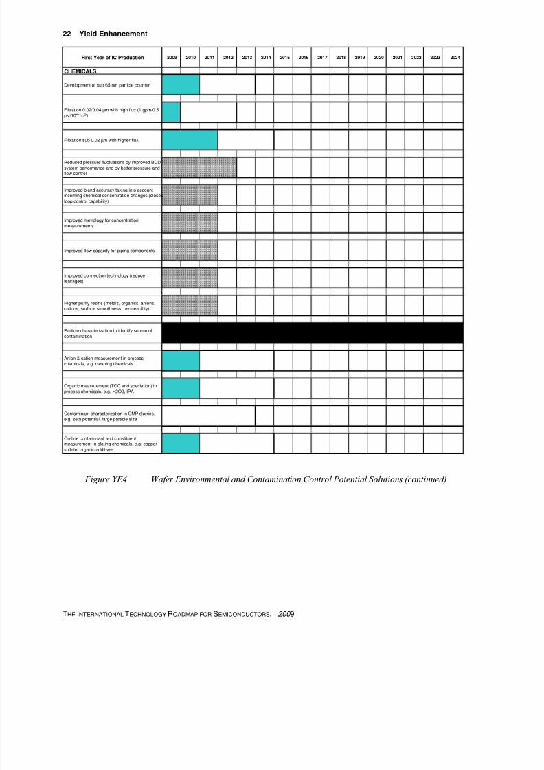
882019 2009_Yield
httpslidepdfcomreaderfull2009yield 2525
Yield Enhancement 23
First Year of IC Production 2009 2010 2011 2012 2013 2014 2015 2016 2017 2018 2019 2020 2021 2022 2023 2024
PRECURSORS
Particle measurement for precursors
Other analyzer techniques for precursors(precursor specific contaminants seesupplementary table)
GASESDevelopment of statistically process c ontrolled(SPC) based specifications for critical specialtygases
Bulk gas purity requirements specifically ofcarrier and purge gases for moisture sensitivematerials
Blending accuracy for low concentrations ofdopant mixtures
Figure YE4 Wafer Environmental and Contamination Control Potential Solutions (continued)