2009 oct. 1 中山電機 黃義佑 1 introduction to the semiconductor industry
TRANSCRIPT

2009 Oct. 1 中山電機 黃義佑 1
Introduction to The Semiconductor Industry

2009 Oct. 1 中山電機 黃義佑 2
PRODUCT APPLICATIONS
INFRASTRUCTURE
Consumers: • Computers• Automotive• Aerospace• Medical• other industries
Customer Service
Original Equipment Manufacturers
Printed Circuit Board Industry
Industry Standards (SIA, SEMI, NIST, etc.)
Production Tools
Utilities
Materials & Chemicals
Metrology Tools
Analytical Laboratories
Technical Work Force
Colleges & Universities
ChipManufacturer
Worldwide sales of microchips : > $250 billion in 2007
SIA: semiconductor industry association
The Semiconductor Industry

2009 Oct. 1 中山電機 黃義佑 3
(1947) The First Solid-state Transistor
Lucent Technologies, Bell Labs Innovations, William Shockley, John Bardeen, Walter Brattain (1956 Nobel Prize in physics)
(1958) The First Integrated Circuit (IC) Device - Oscillator
IC ( 5 components )
Texas Instruments, Inc., Jack Kilby
From Devices to Integrated Circuits
•1950s: Transistor Technology
•1960s: Process Technology
•1970s: Competition
•1980s: Automation
•1990s: Volume Production
(1961) The First Planar IC (Transistor+R+C)
Fairchild Semiconductor, California (Silicon Valley), Robert Noyce

2009 Oct. 1 中山電機 黃義佑 4
Top View of Wafer with Chips
A single integrated circuit, also known as a die, chip, and microchip

2009 Oct. 1 中山電機 黃義佑 5
Snapshot- Profile of IC 8 metal layers – over the past 25 years
Silicon
M6
Via 5
M5
M4
M3
M2
M1
Via 4
Via 3
Via 2
Via 1
Contact(W)
Cu

2009 Oct. 1 中山電機 黃義佑 6
IC Fabrication
Silicon Wafer Wafer Sizes Devices and Layers
Wafer Fab Stages of IC Fabrication
Wafer preparation Wafer fabrication Wafer test/sort Assembly and packaging Final test
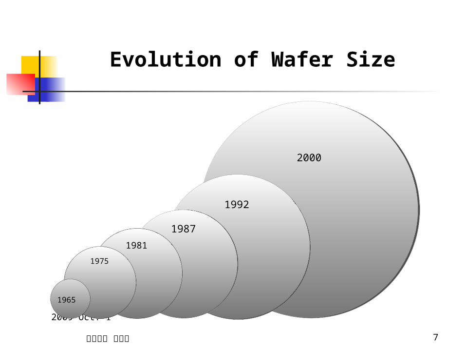
2009 Oct. 1 中山電機 黃義佑 7
Evolution of Wafer Size
2000
1992
1987
1981
1975
1965

2009 Oct. 1 中山電機 黃義佑 8
Devices and Layers from a Silicon Chip
Silicon substrate
drain
Silicon substrate
Top protective layer
Metal layer
Insulation layers
Recessed conductive layer
Conductive layer

2009 Oct. 1 中山電機 黃義佑 9
Stages of IC Fabrication
Wafer Preparationincludes crystalgrowing, rounding,slicing and polishing.
Wafer Fabricationincludes cleaning,layering, patterning,etching and doping.
Assembly and Packaging:
The wafer is cutalong scribe linesto separate each die.
Metal connectionsare made and thechip is encapsulated.
Test/Sort includesprobing, testing andsorting of each die onthe wafer.
Final Test ensures ICpasses electrical andenvironmentaltesting.
Defective die
1.
2.
3.
Scribe line
A single die
Assembly Packaging
4.
5.
Wafers sliced from ingot
Single crystal silicon

2009 Oct. 1 中山電機 黃義佑 10
Preparation of Silicon Wafers
1. Crystal Growth
2. Single Crystal Ingot
3. Crystal Trimming and Diameter Grind
4. Flat Grinding
5. Wafer Slicing
6. Edge Rounding
7. Lapping
8. Wafer Etching
9. Polishong
10. Wafer Inspection
Slurry
Polishing table
Polishing head
Polysilicon Seed crystal
Heater
Crucible
(Note: Terms in Figure 1.7 are explained in Chapter 4.)

2009 Oct. 1 中山電機 黃義佑 11
Wafer Fab
Photo courtesy of Advanced Micro Devices-Dresden, © S. Doering

2009 Oct. 1 中山電機 黃義佑 12
Fab 2 (Hsinchu) Fab 3 (Hsinchu) Fab 5(Hsinchu) Fab 6(Tainan)
Fab 7 (Hsinchu) Fab 8 (Hsinchu) Fab 12 (Hsinchu) Fab 14(Tainan)
TSMC (Shanghai) Wafer Tech (USA) SSMC (Singapore)
TSMC (台積電 )
2009 Oct. 1 中山電機 黃義佑 13
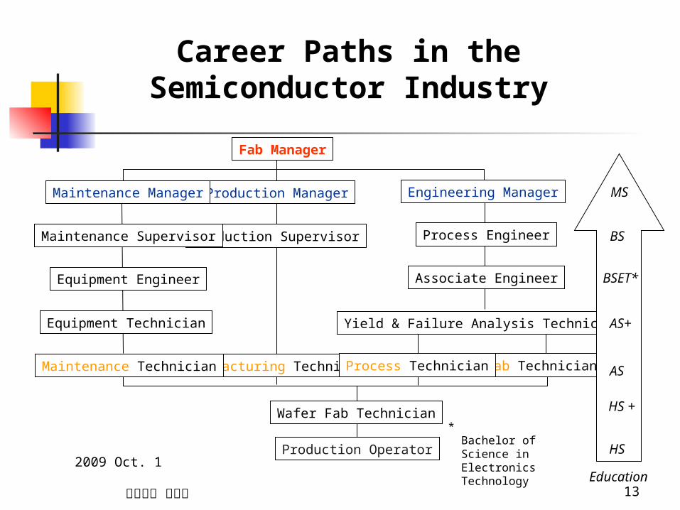
Career Paths in the Semiconductor Industry
Manufacturing Technician
Wafer Fab Technician
Maintenance Technician Lab Technician
Yield & Failure Analysis TechnicianEquipment Technician
Equipment Engineer Associate Engineer
Process EngineerProduction Supervisor
Production Manager
Maintenance Supervisor
Fab Manager
Maintenance Manager
Process Technician
Engineering Manager
Production Operator
HS +
AS+
AS
BS
MS
HS
Education
BSET*
* Bachelor of Science in Electronics Technology

2009 Oct. 1 中山電機 黃義佑 14
Circuit Integration of Semiconductors - Integration Eras
•Increase in Chip Performance
–Components per Chip
–Power Consumption
•Increase in Chip Reliability
•Reduction in Chip Price
Semiconductor Trends :

2009 Oct. 1 中山電機 黃義佑 15
Size Comparison of Early and Modern Semiconductors
1990s Microchip(5~25 million transistors)
1960s Transistor
U.S. coin, 10 cents

2009 Oct. 1 中山電機 黃義佑 16

2009 Oct. 1 中山電機 黃義佑 17
1988 1992 1995 1997 1999 2001 2002 2005
CD(m)
1.0 0.5 0.35 0.25 0.18 0.15 0.13 0.10
Past and Future Technology Nodes for Device Critical Dimension (CD)
Common IC Features
Contact Hole
Line Width Space

2009 Oct. 1 中山電機 黃義佑 18
Feature Technology and Size
150 mm
200 mm
300 mm
Wafer
0.35 m technology
0.25 m technology
0.18 m technology
0.13 mtechnology
0.09 mtechnology
0.065 mtechnology
12-Inch
8-Inch
6-Inch
When compared to the 0.18-micron process, the new 0.13-micron process results in less than 60 percent the die size and nearly 70 percent improvement in performance
The 90-nm process will be manufactured on 300mm wafers
NEC devises low-k film for second-generation 65-nm process

2009 Oct. 1 中山電機 黃義佑 19
TSMC Advanced Technology Overview90 nm (2004) 65 nm (2006) 55 nm (2007) 45 nm (2008) 32/28 nm (2010)

2009 Oct. 1 中山電機 黃義佑 20
Die Size
Wafer photo
Single die
Wafer
From http://www.amd.com

2009 Oct. 1 中山電機 黃義佑 21
Price Decrease of Semiconductor Chips
Redrawn from C. Chang & S. Sze, McGraw-Hill, ULSI Technology, (New York: McGraw-Hill, 1996), xxiii.
1930 1940 1950 1960 1970 1980 1990 2000Year
104
102
1
10-2
10-4
10-6
10-8
10-10
Rel
ativ
e va
lue
Device size = Price =
Bipolar transistor
MSI
LSIVLSI
ULSI
Standard tube
Electron tubes Semiconductor devices
Integrated circuits
Miniature tube
1958 : $10 / 1 Transistor
2001 : $10 / 20 million Transistor
1995 : CD=0.35 μm
1997 : CD=0.25 μm
2002 : CD=0.13 μ m
increase 150~275 chips per wafer

2009 Oct. 1 中山電機 黃義佑 22
Reliability Improvement of Chips & Reduction in Chip Power Consumption per IC
1972 1976 1980 1984 1988 1992 1996 2000
700
600
500
400
300
200
100
0
Year
Lon
g-T
erm
Fai
lure
Rat
e G
oals
in p
arts
per
mil
lion
(P
PM
)
10
8
6
4
2
01997 1999 2001 2003 2006 2009 2012A
vera
ge P
ower
in m
icro
Wat
ts (
10-6 W
)
Year
Redrawn from Semiconductor Industry Association (SIA) National Technology Roadmap, 1997

2009 Oct. 1 中山電機 黃義佑 23
ULSI Chip
Intel Corporation, Pentium III
► Gross world product (GWP) and sales volumes of the electronics, automobile, semiconductor, and steel industries from 1980 to 2000 and projected to 2010.

2009 Oct. 1 中山電機 黃義佑 24
Intel Corporation, Pentium IV

2009 Oct. 1 中山電機 黃義佑 25
► (a) A schematic diagram of the first nonvolatile semiconductor memory (NVSM) with a floating gate. (b) A limiting case of the floating-gate NVSM—the single-electron memory cell.
IC Product #1:
Semiconductor Memory Devices
► Exponential increase of dynamic random access memory (DRAM) density versus year based on the Semiconductor Industry Association (SIA) roadmap.
NVSM : non-volatility; high device density; low-power consumption; electrical rewritability.

2009 Oct. 1 中山電機 黃義佑 26
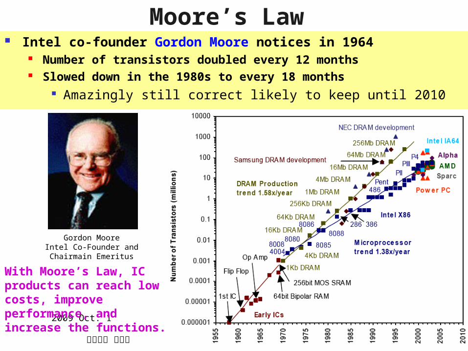
IC Product #2 : Microprocessor Chips Moore’s Law for Microprocessors
Advanced Micro Devices
Intel Corporation
Year
4004
8080
8086
80286
80386
80486
Pentium Pentium Pro
100M
10M
1M
100K
10K
Tra
nsis
tors
1975 1980 1985 1990 1995 2000
500
25
1.0
.1
.01
Proceedings of the IEEE, January, 1998, © 1998 IEEE
The number of transistors on a chip double every (12) 18 months.
2009 Oct. 1 中山電機 黃義佑 27
Moore’s Law Intel co-founder Gordon Moore notices in 1964
Number of transistors doubled every 12 months Slowed down in the 1980s to every 18 months
Amazingly still correct likely to keep until 2010
With Moore’s Law, IC products can reach low costs, improve performance, and increase the functions.
Gordon MooreIntel Co-Founder and Chairmain
Emeritus

2009 Oct. 1 中山電機 黃義佑 28
Start-Up Cost of Wafer Fabs
$100,000,000,000
$10,000,000,000
$1,000,000,000
$100,000,000
$10,000,000
Cos
t
1970 1980 1990 2000 2010 2020
Year
Actual CostsProjected Costs
Used with permission from Proceedings of IEEE, January, 1998 © 1998 IEEE

2009 Oct. 1 中山電機 黃義佑 29
Productivity Measurements in a Wafer Fab
MetallizationProduction Bay
EtchProduction Bay
Thin FilmsProduction Bay
DiffusionProduction Bay
Photo Production Bay
Ion ImplantProduction Bay
Misprocessing
Production Equipment Inspection
Rework
Inspection
Scrap
Production Equipment Inspection
Production Equipment
InspectionProduction Equipment
InspectionProduction Equipment
InspectionProduction Equipment
Wafer Starts
1 2 3 4
5 6 7 8 9 10 11
12 13 14 15 16 17 18
19 20 21 22 23 24 25
26 27 28 29 30 31
1 2 3 4
5 6 7 8 9 10 11
12 13 14 15 16 17 18
19 20 21 22 23 24 25
26 27 28 29 30 31
1
2 3 4 5 6 7 8
9 10 11 12 13 14 15
16 17 18 19 20 21 22
23 24 25 26 27 28 29
30 31
1
2 3 4 5 6 7 8
9 10 11 12 13 14 15
16 17 18 19 20 21 22
23 24 25 26 27 28 29
30 31
Wafer Outs
Time In Time Out
12
3
6
9
Cycle Timeper Operation
Production Cycle Time = (Date and Time of Wafer Start) - (Date and Time of Wafer Out)
Wafer Outs = Wafer Starts - Wafers Scrapped
Operator Efficiency = Theoretical Cycle Time / Actual Cycle Time
Wafer Moves

2009 Oct. 1 中山電機 黃義佑 30
Equipment Technician in a Wafer Fab
Photograph courtesy of Advanced Micro Devices

2009 Oct. 1 中山電機 黃義佑 31
Technician in Wafer Fab
Photo courtesy of Advanced Micro Devices