20-bit analog-to-digital converter - ti.com · 20-bit analog-to-digital converter ddc101...
TRANSCRIPT

20-BIT ANALOG-TO-DIGITAL CONVERTER
DDC101
DESCRIPTIONThe DDC101 is a precision, wide dynamic range, chargedigitizing A/D converter with 20-bit resolution. Lowlevel current output devices, such as photosensors, can bedirectly connected to its input. The most stringent accu-racy requirements of many unipolar output sensor appli-cations occur at low signal levels. To meet this require-ment, Burr-Brown developed the adaptive delta modula-tion architecture of the DDC101 to provide linearlyimproving noise and linearity errors as the input signallevel decreases. The DDC101 combines the functions ofcurrent-to-voltage conversion, integration, input program-mable gain amplification, A/D conversion, and digitalfiltering to produce precision, wide dynamic range re-sults. The input signal can be a low level current con-nected directly into the unit or a voltage connectedthrough a user selected resistor. Although the DDC101 isoptimized for unipolar signals, it can also accuratelydigitize bipolar input signals. The patented delta modula-
tion topology combines charge integration and digitiza-tion functions. Oversampling and digital filtering reducesystem noise dramatically. Correlated Double Sampling(CDS) captures and eliminates steady state and conver-sion cycle dependent offset and switching errors that arenot eliminated with conventional analog circuits.
The DDC101 block diagram is shown below. Duringconversion, the input signal is collected on the internalintegration capacitance for a user determined integrationperiod. A high precision, autozeroed comparator samplesthe analog input node. Tracking logic updates the internalhigh resolution D/A converter at a 2MHz rate to maintainthe analog input at virtual ground. A user programmabledigital filter oversamples the tracking logic’s output. Thedigital filter passes a low noise, high resolution digitaloutput to the serial I/O register. The serial outputs ofmultiple DDC101 units can be easily connected togetherin series or parallel if desired to minimize interconnections.
MONOLITHIC CHARGE INPUT ADC
DIGITAL FILTER NOISE REDUCTION:0.9ppm, rms
DIGITAL ERROR CORRECTION: CDS
CONVERSION RATE: Up to 15kHz
USER FRIENDLY EVALUATION FIXTURE
APPLICATIONSFEATURES DIRECT PHOTOSENSOR DIGITIZATION
PRECISION INSTRUMENTATION
INFRARED PYROMETRY
PRECISION PROCESS CONTROL
CT SCANNER DAS
CHEMICAL ANALYZERS
CINT
Digital Integration,Tracking andControl Logic
Digital Filter andError Correction
Serial I/ORegister
Serial InSerial Out
Reset
DAC
CDAC
DDC101 Integrated Circuit
Comparator
VREF
AnalogInput
Ground
Setup
OversampledDigital Out
18 Bits
20 Bits
Test In +VS
Test Current
©1993 Burr-Brown Corporation PDS-1211E Printed in U.S.A. March, 1998
®
International Airport Industrial Park • Mailing Address: PO Box 11400, Tucson, AZ 85734 • Street Address: 6730 S. Tucson Bl vd., Tucson, AZ 85706 • Tel: (520) 746-1111 • Twx: 910-952-1111Internet: http://www.burr-brown.com/ • FAXLine: (800) 548-6133 (US/Canada Only) • Cable: BBRCORP • Telex: 066-6491 • FA X: (520) 889-1510 • Immediate Product Info: (800) 548-6132
DDC101
SBAS029

®
DDC101 2
TABLE OF CONTENTSSection 1 ............. Basic Theory of Operation
2 ............. Specifications
3 ............. Pin Descriptions
4 ............. Timing Diagrams
5 ............. Discussion of Specifications
6 ............. Detailed Theory of Operation
7 ............. Applications Information
8 ............. Mechanical
The second block diagram, Figure 2, shows the DDC101circuit architecture which implements these functionsmonolithically. During each conversion, the input signalcurrent is collected on the internal integration capacitance,CINT, as charge for a user determined integration period, TINT.As the integration capacitor collects input charge, the track-ing logic updates the internal high resolution D/A converterat a 2MHz rate to maintain the analog input node at virtualground.
The digital filter oversamples the tracking logic’s output atthe beginning and end of each integration period to producetwo oversampled data points. The DDC101 measures thecharge accumulated in the integration and performs corre-lated double sampling (CDS) by subtracting these two datapoints. CDS eliminates integration cycle dependent errorssuch as charge injection, offset voltage, and reset noise sincethese errors are measured with the signal at each of the twodata points. The number of oversamples, and thus the fre-quency response of the digital filter, is user programmable.
The digital filter passes a low noise, high resolution digitaloutput to the serial I/O register. Since the timing control ofthe serial I/O register is independent of the DDC101 conver-sion process, the outputs of multiple DDC101 units can beconnected together in series or parallel to minimize intercon-nections.
SECTION 1BASIC THEORY OF OPERATIONThe basic function of the DDC101 is illustrated in theSimplified Equivalent Circuit shown in Figure 1. The opera-tion is equivalent to the functions performed by a very highquality, low bias current switched integrator followed by aprecision floating point programmable gain amplifier andending with a high resolution A/D converter.
FIGURE 1. Simplified Equivalent Circuit of DDC101 to Illustrate Function.
FIGURE 2. DDC101 Block Diagram.
CINT
Digital Integration,Tracking andControl Logic
Digital Filter andError Correction
Serial I/ORegister
Serial InSerial Out
Reset
DAC
CDAC
DDC101 Integrated Circuit
Comparator
VREF
AnalogInput
Ground
Setup
OversampledDigital Out
18 Bits
20 Bits
Test In +VS
Test Current
CINT
Data Out
Reset
Switched Integrator Programmable GainAmplifier
A/D Converterand Control Logic
Sensor
i Signal

3 DDC101®
The information provided herein is believed to be reliable; however, BURR-BROWN assumes no responsibility for inaccuracies or omissions. BURR-BROWNassumes no responsibility for the use of this information, and all use of such information shall be entirely at the user’s own risk. Prices and specifications are subjectto change without notice. No patent rights or licenses to any of the circuits described herein are implied or granted to any third party. BURR-BROWN does notauthorize or warrant any BURR-BROWN product for use in life support devices and/or systems.
An internal test current source is provided for basic func-tionality testing and diagnostics. This approximately 100nAcurrent source is pin activated and sums with the externalinput current.
Figure 3 shows a more detailed circuit configuration of theDDC101. The single integration capacitor, CINT, and theD/A converter have been replaced with a high resolution
Capacitor Digital-to-Analog Converter (CDAC). By switch-ing between ground and VREF the binary weighted capacitorarray of the CDAC accumulates the input signal’s charge tokeep the comparator input at virtual ground.
FIGURE 3. DDC101 Detailed Circuit Diagram.
Reset
ComparatorSensor
Serial I/ORegister
DATAINPUT
DATAOUTPUT
HighResolutionDigital Out
3rd Order DigitalIntegration,
Tracking andControl Logic
DigitalFilter
OversampledDigital Out
CINT
Buffer
VREF SYSTEMCLOCK
System Control DATACLOCK
DATATRANSMIT
CDAC
DDC101+VS
Test Current
TESTIn
ANALOGIn
ANALOGCOMMON
18 Bits 20 Bits

®
DDC101 4
SECTION 2SPECIFICATIONSELECTRICALAll specifications with unipolar current input range, TINT = 1ms, correlated double sampling enabled, System Clock = 2MHz, VREF = –2.5V, TA = +25°C and VS = ±5VDC,unless otherwise noted.
DDC101
PARAMETER CONDITIONS MIN TYP MAX UNITS
INPUTSCharge Input(6)
Unipolar Input Range BTC Output Code –1.95 500 pC/IntegrationBipolar Input Range BTC Output Code –251.95 250 pC/Integration
Input Current Unipolar or Bipolar Range 7.8 µACurrent Input Range Examples(10)
Unipolar Input Range TINT
= 100µs –0.0195 5 µAUnipolar Input Range TINT = 1ms –1.95 500 nABipolar Input Range TINT = 100µs –2.5195 2.5 µABipolar Input Range TINT = 1ms –251.95 250 nA
Voltage Input Examples(10)
Unipolar Input Range(2) RIN
= 10MΩ, TINT
= 1ms –0.0195 5 VBipolar Input Range(2) RIN = 10MΩ, TINT = 1ms –2.5195 2.5 V
DYNAMIC CHARACTERISTICSConversion Time 64 256 x 106 µsIntegration Time 64 106 µsSystem Clock Input 0.5 2 MHz
ACCURACYUnipolar Mode Noise
Noise, Low Level Current Input(1) CSENSOR = 0pF, L = 8 0.9 ppm of FSR, rms(3)
Noise, Low Level Current Input(1) CSENSOR = 0pF, L = 1 1.6 ppm of FSR, rmsNoise, Low Level Current Input(1) C
SENSOR = 100pF, L = 1 2.1 3 ppm of FSR, rms
Noise, Low Level Current Input(1) CSENSOR = 500pF, L = 1 4.2 ppm of FSR, rmsNoise, Voltage Input(1, 2) RIN ≥ 20MΩ 1.9 ppm of FSR, rms
Differential Linearity ErrorUnipolar Input Range Entire Range ±0.005% Reading ±0.5ppm FSR, max
0.1% FSR Input ±0.00006 % of FSR1% FSR Input ±0.00010 % of FSR10% FSR Input ±0.00055 % of FSR
Unipolar or Bipolar Input Range ±0.0015 % of FSRIntegral Linearity Error
Unipolar Input Range(11) 0 to 500 pc/Integration ±0.0244% Reading ±2.5ppm FSR, max–1.95 to 0 pc/Integration ±0.0244% Reading ±3.0ppm FSR, max
0.1% FSR Input ±0.00028 % of FSR1% FSR Input ±0.00050 % of FSR10% FSR Input ±0.0027 % of FSR
Unipolar or Bipolar Input Range(11) ±0.003 % of FSRNo Missing Codes
Unipolar Input Range 18 BitsBipolar Input Range 16 Bits
Input Bias Current TA = +25°C 3 10 pA
DC Gain Error ±0.5 ±2 % of FSROutput Offset Error(8) ±0.5 ppm of FSRInput Offset Voltage(8) ±0.5 ±2 mVExternal Voltage Reference, VREF –2.5 VDCInternal Test Signal 100 nAInternal Test Signal Accuracy ±20 nAGain Sensitivity to VREF VREF = 2.5V ±0.1V 1:1PSRR 80 90 dB
PERFORMANCE OVER TEMPERATUREOutput Offset Drift(8) not including bias current drift 0 µV/°CInput Offset Voltage Drift(8) 1 µV/°CInput Bias Current Drift +25°C to +45°C 0.1 0.5 pA/°CInput Bias Current T
A = +85°C 8 40 pA
Gain Drift(4) ±15 ppm/°C
DIGITAL INPUT/OUTPUTLogic Family TTL Compatible CMOSLogic Level: VIH IIH = +5µA +2.0 +VCC V
VIL IIL = +5µA –0.3 +0.8 VVOH IOH = 2 TTL Loads +2.4 +VCC VV
OLIOL
= 2 TTL Loads 0.0 0.4 VData Clock
Data I/O 8 MHzSETUP Code I/O(9) 4 MHz
Data FormatStraight Binary Unipolar or Bipolar Range 20 BitsTwo’s Complement Unipolar or Bipolar Range 21 Bits

5 DDC101®
SPECIFICATIONS (CONT)
ELECTRICALAll specifications with unipolar current input range, TINT = 1ms, correlated double sampling enabled, System Clock = 2MHz, VREF = –2.5V, TA = +25°C and VS = ±5VDC,unless otherwise noted.
DDC101
PARAMETER CONDITIONS MIN TYP MAX UNITS
POWER SUPPLY REQUIREMENTSOperation(5) ±4.75 ±5 ±5.25 VDCQuiescent Current, Positive Supply VS+ = +5VDC, VDD+ = +5VDC 15.6 19.5 mA
Analog, VS+ 8.9 mADigital, VDD+ 6.7 mA
Quiescent Current, Negative Supply VS– = –5VDC 18.0 22.5 mA
Operating Power 170 mW
TEMPERATURE RANGEOperating –40 +85 °CStorage –60 +100 °C
NOTES: (1) Input = low level (less than 1% of Full Scale); Full Scale IIN = 500nA; TINT = 1ms; Unipolar Input Range; Acquisition Time = 16 clock cycles, Oversampling = 128. (2) Voltage input is converted through userprovided input resistor, R
IN. (3) FSR is Full Scale Range. (4) Gain Drift does not include the drift of the external reference. (5) V
DD+ must be less than or equal to V
S+. See Section 7 for recommended connections. (6)
Straight Binary output code has slightly different Charge Range. See Section 6. (8) Input offset voltage is nulled by autozero circuitry and causes no output error. See Section 6 (Internal Error Correction). (9) This isthe maximum clock frequency at which SETUP codes can be written to and read from the DDC101. (10) For other input current and voltage configurations, see Discussion of Specifications and Detailed Theory of Operationsections. (11) A best-fit straight line method is used to determine linearity. Two different best-fit straight lines are used for the two unipolar integral linearity specifications. Acquisition Time = 16 clock cycles, Oversampling= 128.
Analog InputsInput Current ............................................................ 100mA, momentaryInput Current .............................................................. 10mA, continuousInput Voltage ................................................... VS+ +0.5V to VS– –0.5V
Power SupplyVS+ .................................................................................................. + 7VVS– .................................................................................................... –7VVDD+ ................................................................................. must be ≤ VS+
Maximum Junction Temperature ................................................... +165°C
ABSOLUTE MAXIMUM RATINGS
PACKAGE/ORDERING INFORMATION
PACKAGE THERMALDRAWING RESISTANCE (θJA)
PRODUCT PACKAGE NUMBER (1) (°C/W)
DDC101U 24-Lead SOIC 239 100
NOTE: (1) For detailed drawing and dimension table, please see end of datasheet, or Appendix C of Burr-Brown IC Data Book.
The information provided herein is believed to be reliable; however, BURR-BROWN assumes no responsibility for inaccuracies or omissions. BURR-BROWN assumesno responsibility for the use of this information, and all use of such information shall be entirely at the user’s own risk. Prices and specifications are subject to changewithout notice. No patent rights or licenses to any of the circuits described herein are implied or granted to any third party. BURR-BROWN does not authorize or warrantany BURR-BROWN product for use in life support devices and/or systems.
ELECTROSTATICDISCHARGE SENSITIVITY
This integrated circuit can be damaged by ESD. Burr-Brownrecommends that all integrated circuits be handled with ap-propriate precautions. Failure to observe proper handling andinstallation procedures can cause damage.
ESD damage can range from subtle performance degradationto complete device failure. Precision integrated circuits maybe more susceptible to damage because very small parametricchanges could cause the device not to meet publishedspecifications.

®
DDC101 6
PIN CONFIGURATION
Top View 24-Lead SOIC
SECTION 3PIN DESCRIPTIONS
1
2
3
4
5
6
7
8
9
10
11
12
24
23
22
21
20
19
18
17
16
15
14
13
REFERENCE BUFFER BYPASS
VREF
TEST In
RESET SETUP In
SETUP
READ DATA/SETUP
DATA TRANSMIT In
OVERFLOW + Out
OVERFLOW – Out
DATA VALID Out
DATA OUTPUT
DIGITAL GROUND
VS–, ANALOG
ANALOG COMMON
ANALOG In
ANALOG COMMON
VS+, ANALOG
VS+, ANALOG
RESET SYSTEM In
FDS (Final Data Point Start) In
SYSTEM CLOCK
DATA CLOCK
DATA INPUT
VDD+, DIGITAL
PINNUMBER NAME DESCRIPTION
1 VS–, ANALOG Negative analog power supply voltage, –5VDC.
2 ANALOG COMMON Analog ground point.
3 ANALOG INPUT Input for low level current signal. Photosensor can be directly connected to this input. With a resistor in series,DDC101 will convert a voltage input.
4 ANALOG COMMON Analog ground point.
5 VS+, ANALOG Positive analog power supply voltage, +5VDC. Hardwire to pin 6.
6 VS+, ANALOG Positive analog power supply voltage, +5VDC. Hardwire to pin 5.
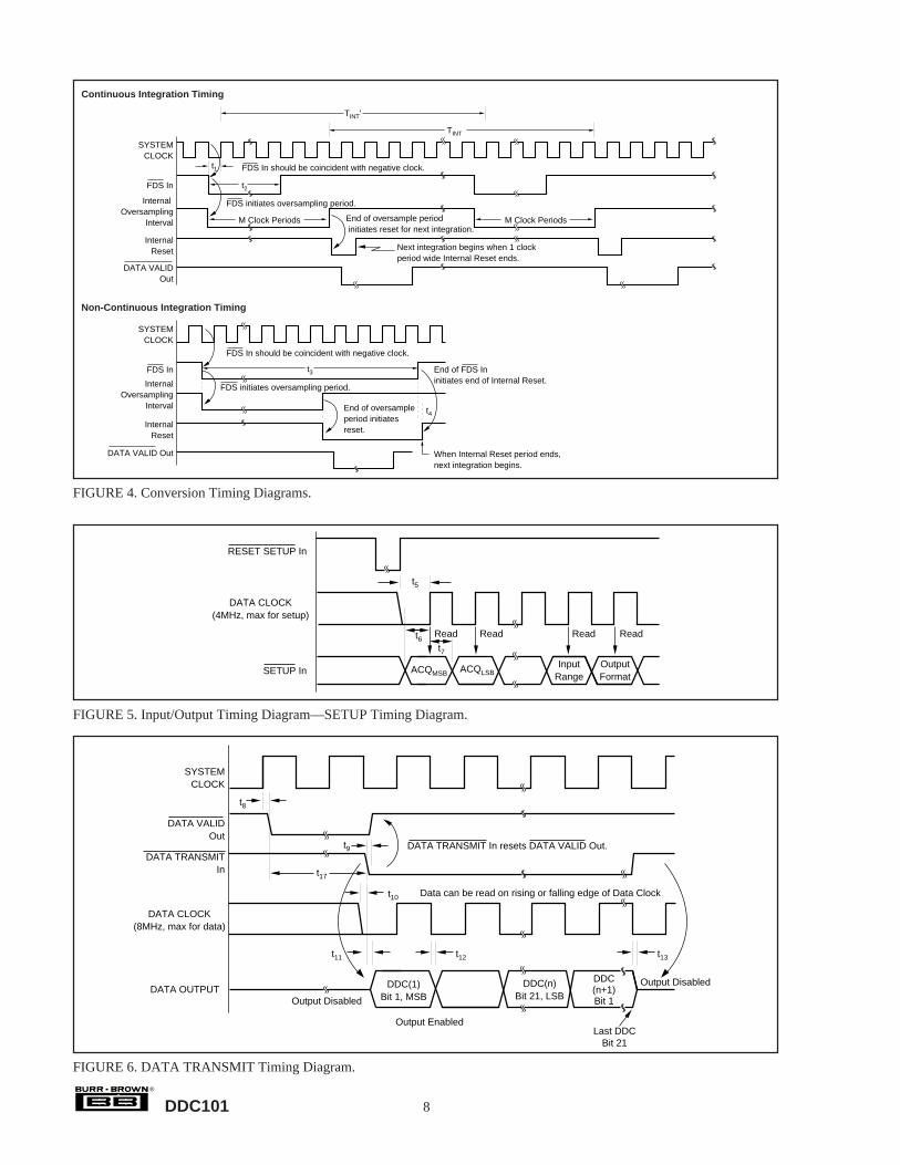
7 RESET SYSTEM In This input resets DDC101, but does not reset the SETUP register. The DDC101 system is reset when this pinis active; reset action is removed when the pin is inactive.
8 FDS In This is Final Data point Start input. This input is the basic user control of the integration and conversion timing.When it becomes active, the DDC101 starts collection of the M, final data point samples. The beginning of thenext integration time is exactly M system clock periods after the Final Data point Start command when operatingin the continuous mode.
9 SYSTEM CLOCK This clock input sets the basic sampling rate of the DDC101. The DDC101 is specified with a clock speed of2MHz. The clock speed can be 0.5MHz to 2.0MHz.
10 DATA CLOCK This clock input controls the data transfer rate for the serial DATA INPUT and DATA OUTPUT ports. The DATACLOCK is independent of the SYSTEM CLOCK. This allows the DATA CLOCK to be operated at higher or lowerspeeds than the SYSTEM CLOCK. For best noise performance, data should not be transmitted and the DATACLOCK should not be active during the initial and final data point collection. If data is being transmitted duringthe initial and final data point collection periods, the DATA CLOCK should be synchronized to the SYSTEMCLOCK, to minimize added noise. DATA CLOCK can be connected to SYSTEM CLOCK, so that the same clockis used for both; however, for best noise performance, the DATA CLOCK input should be active only when datais transmitted.
11 DATA INPUT This input can be used to “daisy chain” the output of several DDC101s together to minimize wiring. The outputregister of the DDC101 acts as a shift register to pass through the output of previously connected DDC101 units.In this way, multiple DDC101 units can convert simultaneously then sequence the data out serially on the samedata line with one common control line and one common data line for all DDC101 units.
12 VDD+, DIGITAL Digital power supply, +5VDC. VDD+ must be less than or equal to VS+.
13 DIGITAL GROUND Digital ground point.
14 DATA OUTPUT This output provides serial digital data clocked out at user controlled DATA CLOCK rate. Output data formatis a 21-bit Binary Two's Complement word or a 20-bit Straight Binary word. The data word is transmitted MSBfirst. When DATA TRANSMIT is not active DATA OUTPUT tri-states.
15 DATA VALID This output is activated when conversion is complete and remains active until the DATA TRANSMIT input isactivated.
16 OVERFLOW– The OVERFLOW output signals each provide an open collector output so that the overflow outputs from several
17 OVERFLOW+ DDC101s can easily be connected (wire ORed) together to a common pull-up resistor. They are activated whenthe input is beyond the acceptable range during conversion. Specifically, they are activated when the internalD/A converter input or digital filter exceeds full scale. They are Cleared at the end of conversion 1/2 clock cycleafter DATA VALID high. DATA VALID can be used to capture OVERFLOW data into an external register.

7 DDC101®
PIN DESCRIPTIONS (CONT)
PINNUMBER NAME DESCRIPTION
18 DATA TRANSMIT In This input controls the transmission of data from the serial I/O register of the DDC101. It can be activatedanytime after DATA VALID out becomes active. It must remain active until all data has been collected from theserial I/O register(s) of all DDC101s in the data path.
19 READ DATA/ This input can be used to read back the current SETUP data. When this input is held high, the output from DATASETUP In OUTPUT is the data collected by the DDC101. When this input is pulled low, an internal shift register is loaded
with the current SETUP data on the rising edge of DATA CLOCK. This SETUP data shift register is logicallyconnected between DATA INPUT and DATA OUTPUT pins and can be read in the same way that the dataoutput is read. SETUP data read back does not invalidate data already stored in the DDC101's serial I/O registeror data being collected by the DDC101, although digital noise concerns should be considered asdiscussed in DATA CLOCK.
20 SETUP In This input pin controls the DDC101 SETUP. A 12-bit digital word transmitted into this pin controls AcquisitionTime, K, Oversampling, M, Multiple Integrations, L, Input Range and Output Data Format. The DDC101 readsthe SETUP code at this pin after the RESET SETUP input transitions from active to inactive. The SETUP codeis read into the SETUP register on the 12 positive data clock transitions following that transition.
21 RESET SETUP Resets SETUP register only, does not reset balance of DDC101. The DDC101 reads SETUP input data afterthis input transitions from active (reset) to inactive.
22 TEST In This is a digital input that controls the connection of an internal DC current source to the DDC101's input. TESTIn exercises the DDC101 and is intended to test for functionality only. The typical test input current is 100nA±20nA. The quiescent current of the DDC101 increases by approximately 1mA when TEST In is active. WhenTEST is HIGH, the internal current source is ON and current is flowing into the DDC101 input. When TEST isLOW, the current source is disconnected from the input.
23 VREF An external –2.5V reference must be connected to the REFERENCE In pin. Use of an external reference allowsmultiple DDC101s to use the same system reference for optimum channel matching. The external referenceshould be filtered to minimize noise contribution (see Figure 24).
24 REFERENCE An external capacitor of 10µF should be connected to this node to provide proper operation of the internalBUFFER BYPASS D/A converter. The REFERENCE In pin is connected to an internal reference bufferamplifier. The internal reference buffer drives the internal CDAC. This buffer output is not intended for externaluse.
SECTION 4TIMING CHARACTERISTICSAll specifications with Unipolar input range, TINT = 1ms, Current Input, Correlated Double Sampling enabled, Sys Clock = 2MHz, VREF = –2.5V, TA = +25°C and
VS = ±5VDC, unless otherwise noted.
SYMBOL DESCRIPTION MIN TYP MAX UNITS
t1 FDS Setup 30 ns
t2 FDS width, Continuous Conversion 50 (M–1) Clocks+t1+100ns ns
t3 FDS width, Asynchronous Conversion M Clocks+t1 ns
t4 FDS HIGH to start of next integration, Asynchronous Conversion 50 ns
t5 Setup time for RESET SETUP HIGH to DATA CLOCK HIGH 60 ns
t6 Setup time for Setup Codes data valid before rising edge of DATA Clock 30 ns
t7 Hold time for Setup Codes data valid after rising edge of DATA Clock 30 ns
t8 Propagation delay from rising edge of SYSTEM CLOCK to DATA VALID LOW 50 ns
t9 Propagation delay from DATA TRANSMIT LOW to DATA VALID HIGH 35 ns
t10 Setup time for DATA CLOCK LOW to DATA TRANSMIT LOW 30 ns
t11 Propagation delay from DATA TRANSMIT LOW to valid data out 30 ns
t12 Hold time that Data output is valid after falling edge of DATA CLOCK 10 ns
t13 Propagation delay from DATA TRANSMIT HIGH to Data Output tri-stated 40 ns
t14 Propagation delay from falling edge of SYSTEM CLOCK to OVERFLOW+ and 25 ns
OVERFLOW–cleared
t15 SYSTEM CLOCK pulse width HIGH 240 ns
t16 SYSTEM CLOCK pulse width LOW 240 ns
t17 DATA VALID LOW to DATA TRANSMIT LOW, Single DDC101 30 (LxN–21) Clocks ns
®
DDC101 8
FIGURE 6. DATA TRANSMIT Timing Diagram.
FIGURE 4. Conversion Timing Diagrams.
InputRange
OutputFormat
SETUP In
DATA CLOCK(4MHz, max for setup)
ACQLSB
t5
RESET SETUP In
ACQMSB
Read Read Read Readt6t7
FIGURE 5. Input/Output Timing Diagram—SETUP Timing Diagram.
SYSTEMCLOCK
DATA VALIDOut
DATA TRANSMITIn
DATA OUTPUT
DATA CLOCK(8MHz, max for data)
t10
DDC(1)Bit 1, MSB
DDC(n)Bit 21, LSB
DDC(n+1)Bit 1
Output Disabled
Last DDCBit 21
Output Enabled
Output Disabled
t12
Data can be read on rising or falling edge of Data Clock
DATA TRANSMIT In resets DATA VALID Out.t9
t11 t13
t17
t8
Continuous Integration Timing
Non-Continuous Integration Timing
SYSTEMCLOCK
FDS In
Internal Oversampling
Interval
InternalReset
SYSTEMCLOCK
FDS In
InternalOversampling
Interval
InternalReset
FDS In should be coincident with negative clock.
FDS initiates oversampling period.
M Clock Periods End of oversample period initiates reset for next integration.
FDS In should be coincident with negative clock.
FDS initiates oversampling period.
End of FDS Ininitiates end of Internal Reset.
End of oversample period initiates reset.
When Internal Reset period ends, next integration begins.
DATA VALIDOut
t2
t1
t3
DATA VALID Out
Next integration begins when 1 clockperiod wide Internal Reset ends.
M Clock Periods
t4
TINT'
TINT

9 DDC101®
TIMING DIAGRAMS (CONT)
FIGURE 7. OVERFLOW Out Monitoring Timing Diagram.
OVERFLOW – Out
OVERFLOW + Out
t8
DATA VALID Out
Read
Read Clear
SYSTEM CLOCK In
t14
DATA VALID Out can be used to latch data from the overflow status outputs.
Clear
FIGURE 8. System Clock Timing.
t15SYSTEM CLOCK In
SYSTEM CLOCK
t16

®
DDC101 10
TYPICAL PERFORMANCE CURVESELECTRICALSystem Clock = 2MHz, VS = ±5VDC, VREF = –2.5V, L = 1 Integration/Conversion, and TA = +25°C, unless otherwise noted.
SINAD AT 10kHz CONVERSION, UNIPOLAR INPUT
0
0
20
40
60
80
100500 1000 1500 2000 2500 3000 3500 4000 4500 5000
0dB
–60dB
Input Frequency (Hz)
TH
D +
N (
dB)
100µs Integration TimeK = 16 Acquisition Clocks
M = 32 Oversamples
SINAD AT 1kHz CONVERSION, UNIPOLAR INPUT
0
0
20
40
60
80
10050 100 150 200 250 300 350 400 450 500
0dB
–60dB
Input Frequency (Hz)
TH
D +
N (
dB)
1ms Integration TimeK = 16 Acquisition Clocks
M = 128 Oversamples
NOISE vs INPUT LEVEL (UNIPOLAR) WITH CDS
Noi
se (
ppm
, rm
s)
0 0.1 0.2 0.3 0.4 0.5 0.6 0.7 0.8 0.9 1.0
Input Level of FS
18
16
14
12
10
8
6
4
2
0
CIN = 500pF
CIN = 100pF
CIN = 0pF
1ms Integration TimeK = 16 Acquisition Clocks
M = 128 Oversamples
NOISE vs INPUT LEVEL (UNIPOLAR) WITHOUT CDS
Noi
se (
ppm
, rm
s)
0 0.1 0.2 0.3 0.4 0.5 0.6 0.7 0.8 0.9 1.0
Input Level of FS
18
16
14
12
10
8
6
4
2
0
CIN = 500pF
CIN = 100pF
1ms Integration TimeM = 128 Oversamples
CIN = 0pF
NOISE vs RESISTOR VALUE1000
100
10
1
Noi
se (
ppm
, rm
s)
0.01 0.1 1 10 100 1G
RIN (MΩ)
100µs Int., M = 16 O/S
1ms Int., M = 128 O/S
Low Level, Unipolar InputK = 16 Acquisition Clocks
CHARGE INJECTION vs INPUT CAPACITANCE350
300
250
200
150
100
50
0
–500 100 200 500 1000
CIN (pF)
No CDS
Cha
rge
Inje
ctio
n (p
pm)
CDS On, K = 16

11 DDC101®
TYPICAL PERFORMANCE CURVES (CONT)
ELECTRICALSystem Clock = 2MHz, VS = ±5VDC, VREF = –2.5V, L = 1 Integration/Conversion, and TA = +25°C, unless otherwise noted.
NOISE vs INPUT CAPACITANCE, UNIPOLAR INPUT40
35
30
25
20
15
10
5
00 100 200 500 1000 2000
CIN (pF)
Noi
se (
ppm
, rm
s)
No CDS
CDS On, K = 16
1ms Integration TimeM = 128 Oversamples
CHANGE IN IB vs TEMPERATURE2.0
0
–2.0
–4.0
–6.0
–8.0–40 –20 0 20 40 60 80 100
Temperature (°C)
∆ I B
(pA
)
NOISE vs TEMPERATURE, UNIPOLAR INPUT5
4
3
2
1
0–40 –20 0 25 45 65 85
Temperature (°C)
Noi
se (
ppm
, rm
s)1ms Integration Time
K = 16 Acquisition ClocksM = 128 Oversamples
NOISE vs INTEGRATION TIME, UNIPOLAR INPUT5
4
3
2
1
00.1 1 10 100
Integration Time (ms)
Noi
se (
ppm
, rm
s)
M = 256 O/S
M = 16 O/S
M = 64 O/S
K = 16 Acquisition ClocksCIN = 0pF
INPUT OFFSET VOLTAGE vs INPUT CAPACITANCE0.050
0.000
–0.050
0.100
–0.150
–0.200
–0.250
–0.3000 100 500
VB
IAS (
mV
)
CIN (pF)
NOISE vs OVERSAMPLING, UNIPOLAR INPUT50
10
1.0
0.5
Noi
se (
ppm
, rm
s)
1 2 4 8 16 32 64 128 256
M Oversamples
L = 1 Integration/Conversion
L = 2L = 4L = 8L = 16L = 32
L = 64L = 128
L = 256
1ms Integration TimeK = 16 Acquisition Clocks
CIN = 0pF

®
DDC101 12
NEGATIVE PSRR vs FREQUENCY
0
100
90
80
70
60
50
40
30
20
10
020 40 60 80 100 120 140 160 180 200
PS
RR
(dB
)
100µs Integration TimeK = 16 Acquisition Clocks
M = 32 Oversamples
Frequency (kHz)
POSITIVE PSRR vs FREQUENCY
0
100
90
80
70
60
50
40
30
20
10
020 40 60 80 100 120 140 160 180 200
Frequency (kHz)
PS
RR
(dB
)
1ms Integration TimeK = 16 Acquisition Clocks
M = 128 Oversamples
NEGATIVE PSRR vs FREQUENCY
0
100
90
80
70
60
50
40
30
20
10
020 40 60 80 100 120 140 160 180 200
Frequency (kHz)
PS
RR
(dB
)
1ms Integration TimeK = 16 Acquisition Clocks
M = 128 Oversamples
TYPICAL PERFORMANCE CURVES (CONT)
ELECTRICALSystem Clock = 2MHz, VS = ±5VDC, VREF = –2.5V, L = 1 Integration/Conversion, and TA = +25°C, unless otherwise noted.
POSITIVE PSRR vs FREQUENCY
0
100
90
80
70
60
50
40
30
20
10
020 40 60 80 100 120 140 160 180 200
PS
RR
(dB
)
100µs Integration TimeK = 16 Acquisition Clocks
M = 32 Oversamples
Frequency (kHz)

13 DDC101®
input range, an input current of 0.5µA integrated for 1mswill result in the full scale charge of 500pC. For voltageinputs, the input resistor is chosen to achieve the proper fullscale input current. As an example, for a 5V full scale input,a 10MΩ input resistor is selected to achieve a full scale inputcurrent of 0.5µA (1ms integration time).
Noise of 1.6ppm of FSR is equal to 1.6ppm x 500pC = 0.8fCor 1.6ppm x 0.5µA = 0.8pA or 1.6ppm x 5V = 8µV. Thus,in this instance, noise is 1.6pA or 8µV.
For the unipolar input range, the following table shows thefull scale input current required for different integrationtimes to collect 500pC of charge and the equivalent currentvalues for 2 and 5ppm of FSR.
CURRENT INPUT
The maximum average input current that can be captured bythe DDC101 is ±7.8µA. This current will result in anintegration time of 64µs for unipolar input range and 32µsfor bipolar input range. For longer integration times, theaverage input current must be less.
The maximum input current is limited by the slew andupdate rate of the internal tracking logic and CDAC. Thelargest input current that the DDC101 can accurately track is7.8µA. Input currents larger than 7.8µA and high speedcurrent input pulses can be accurately captured and digitizedby the DDC101 with an external input or sensor capacitanceon the DDC101 input. The average current during a com-plete integration cycle cannot exceed 7.8µA. Likewise, thetotal charge input must not exceed 500pC unipolar, 250pCbipolar during the integration time.
An external user provided input capacitance, CS, as shown inFigure 9a, will capture the input signal charge if the inputcurrent limit is temporarily exceeded during the integrationcycle. The DDC101 will then transfer the charge completelyto CINT based upon conservation of charge. An additional
FIGURE 9a. Current Pulse Input Capture.
TABLE I. Integration Time (TINT
) and Full Scale Current (IFS
)for Full Scale 500pC Integration.
TINT IFS 2ppm 5ppm
50ms 10nA 0.02pA 0.5pA5ms 100nA 0.2pA 1pA1ms 500nA 1pA 2.5pA
500µs 1µA 2pA 5pA100µs 5µA 10pA 25pA
i
DDC101CS V
Voltage across input must not exceed ±2.5V.
Analog Input, pin 3
Analog Common
External user provided capacitance, CSOURCE, to store current pulses.
SECTION 5DISCUSSION OFSPECIFICATIONS
INPUT
The DDC101 is a charge digitizing A/D converter. Lowlevel current output sources, such as a photosensors, can bedirectly connected to its input. The input signal can also bea voltage connected through a user selected resistor.
CHARGE INPUT
The maximum charge that can be captured in one integrationby the DDC101 is 500pC. In the unipolar input range mode,the maximum positive charge that can be collected in oneintegration is 500pC. The DDC101 has a small negativerange in the unipolar mode of –1.95pC. This small negativeunderrange is included to allow for a small amount ofleakage current from the user’s PC board and sensor. In thebipolar input range, the maximum positive charge that canbe collected is +250pC. The maximum negative charge thatcan be collected is –251.95pC.
In addition to the normal mode of one integration perconversion, DDC101 can be configured by the user for 1 to256 integrations per conversion. When the multiple integra-tions per conversion mode is chosen, the DDC101 DSPcircuitry internally averages multiple integration cycles toprovide one conversion result. This result has lower noisebecause it is the average of multiple integrations. In thismode, the maximum total charge that can be captured by theDDC101 in 256 integrations is 128,000pC.
TEST CURRENT INPUT
An internal DC test current can be connected under usercontrol to the DDC101’s input. The test current is nominally100nA and will be summed with any applied external inputsignal. It is derived by a resistive network from the positivepower supply. The test current is intended to test for func-tionality only. The TEST In pin of the DDC101 controls thecurrent. When TEST is HIGH, the internal current source isON and current is flowing into the DDC101 input. WhenTEST is LOW, the current source is disconnected from theinput. With TEST active, positive power supply currentincreases by approximately 1mA.
FULL SCALE RANGE
The full scale range (FSR), which is referenced in thespecification table, is the difference between the positive fullscale charge and the negative full scale charge for theDDC101 in one integration cycle. Specifications such asnoise and linearity, which are specified in percent or ppm ofFSR, are referring to a value of 500pC for both unipolar andbipolar input ranges.
The full scale input current for a given integration time willresult in a full scale input charge. As an example for unipolar

®
DDC101 14
constraint is, the voltage that appears at the DDC101 input,must not exceed 2.5V. If this voltage is exceeded, chargemay be lost and the integration result may be invalid. Theinput voltage can be calculated:
maximum input voltage based upon several selections ofinput current and input resistor for unipolar input range. Theaccuracy of the input resistor will add directly to the DCGain Error of the DDC101; the drift of the input resistor willadd directly to the Gain Drift of the DDC101.
Note that the DDC101 output noise decreases as RIN in-creases. This is because the DDC101 noise gain decreasesand the input resistance current noise decreases as RIN
increases. This effect is shown in the “Noise vs ResistorValue” typical performance curve.
FIGURE 9b. DDC101 Input Configurations.
i
InputResistor
DDC101RINV
i
DDC101
Data Out
Data Out
Analog Input, pin 3
Analog Common
Analog Input, pin 3
Analog Common
Voltage Input Configuration
Current Input Configuration
Line
arity
Err
or (
% o
f FS
R)
0.1
0.01
0.001
0.0001
Unipolar Input Level (% of FSR)
0.001 0.01 0.1 1 10 100
FIGURE 10. Maximum Unipolar Integral Linearity ErrorRelative to Full-Scale, Converted From % ofReading Specification.
i(t) = CSdvdt
or
V = 1CS
i(t)dt∫
therefore,
V = it
CS
.
The current pulse must occur completely during part of oneDDC101 integration time, and the DDC101 must still havetime to discharge the input capacitance to ground at amaximum rate of 7.8µA before the DDC101 is triggered(through the FDS input) to end the integration. In addition,the total charge integrated must be 500pC or less for theunipolar range. A current pulse of 100µA for 2µs creates200pC of charge.
VOLTAGE INPUT SPECIFICATIONS
The DDC101 is a charge digitizing device. With a userprovided input resistor, the DDC101 can digitize voltageinputs. All of the general charge/current input specificationsapply to the voltage input situation. The specification tableshows the typical noise of the DDC101 including the effectsof a 20MΩ input resistor, RIN.
The input of the DDC101 is a virtual ground. A voltage inputcauses a current, i, to flow into the input through RIN asshown in Figure 9b. The maximum input current is deter-mined by the integration time selected. Table II shows the
V = 100µA( ) •2µs
100pF= 2V.
As an example, with a user supplied input capacitance of100pF, a current pulse of 100µA for 2µs could be storedwithout exceeding 2.5V applied to the input:
INPUT RESISTOR, RIN
INTEGRATION TIME 1ms 500 µs 100µs
Full Scale Input Current 0.5µA 1µA 5µA
Full Scale Voltage50mV 100kΩ 50kΩ 10kΩ500mV 1MΩ 500kΩ 100kΩ5V 10MΩ 5MΩ 1MΩ50V 100MΩ 50MΩ 10MΩ
TABLE II. Example of Input Resistor Values Unipolar InputRange.
UNIPOLAR LINEARITY ERRORS
Due to innovative design techniques, the absolute level oflinearity error of the DDC101 improves as the input signallevel decreases when used in the unipolar input mode.Therefore, in unipolar input mode, the integral linearity ofthe DDC101 is specified as a small base error plus apercentage of reading error or as a percentage of full scalerange. A best-fit straight line method is used to determineintegral linearity. Two different best-fit straight lines areused for the two unipolar integral linearity specifications.For bipolar input mode, linearity is specified only as apercentage of full scale range.
To illustrate the improvement in unipolar mode linearityerror, Figure 10 shows the maximum unipolar integral lin-earity error (ILE) of the DDC101 as a function of the inputsignal level. The maximum integral linearity error is±0.0244% of reading ±2.5ppm of FSR (ILE max for unipo-lar input of –1.95 to 0 pc is ±0.0244% of reading ±3.0ppmof FSR). Thus, the maximum ILE for an input level of 1%of FSR is 0.0005%FSR.

15 DDC101®
2. OversamplingThis is the low pass filter characteristic of the digitalfilter’s oversampling. This response reduces the broad-band noise in the input signal and the DDC101. Broad-band noise decreases as the number of oversamplesincreases.
3. Multiple IntegrationsThis is the low pass filter characteristic that results whenthe digital filter is used to average multiple integrations.This will determine the primary response of the DDC101if two or more integrations are internally averaged.
See Section 6 for more details.
SECTION 6DETAILED THEORYOF OPERATIONINTEGRATION CYCLE
An integration cycle, as illustrated in Figure 11, includes theAcquisition Time, Initial Data Point Sampling, TrackingInterval, and Final Data Point Sampling. The AcquisitionTime is K clock periods. The first clock cycle of theAcquisition Time is used to reset the integrating capacitor,CINT, to zero from the previous integration. The balance ofthe Acquisition Time insures that the DDC101 system isaccurately tracking the input signal prior to initial data pointacquisition. Close-ups of the Reset and Acquisition time areshown in Figures 12 and 13.
The Initial Data Point is then sampled M times. The Integra-tion cycle time consists primarily of the Tracking Intervalduring which time the DDC101 “tracks” the integration ofthe input signal. The Tracking Interval is followed by themeasurement of the Final Data Point with the same userselected number of samples, M. M and K are user selectable.The entire integration cycle consists of N clock periods ascontrolled by the user.
The DDC101 operates in continuous and non-continuousintegration modes. In the continuous mode, one integrationfollows another with no delay from the end of one integra-tion to the beginning of the next conversion. In the non-continuous mode, each new integration is started separatelyunder user control.
The Final Data point Start (FDS) input is the primary usercontrol of the integration cycle. The FDS input controls theend of one integration cycle and the start of the nextintegration cycle in both the continuous and non-continuousintegration modes. Measurement of the M final data pointsamples begins when the FDS input is activated.
CONTINUOUS INTEGRATION MODE
In the continuous integration mode, the “Final Data PointStart” command (using the FDS pin) initiates the measure-ment of the M final data point samples. The next integrationcycle begins immediately after the final data point sampling
NOISE
The noise of the DDC101 improves as the input signal leveldecreases, thus very low level signals can be resolved. Noiseis shown in the specification table for low level inputs. Forunipolar input range, the DDC101 noise at low level inputsis dominated by comparator noise gained to the output; atfull scale inputs, the noise is dominated by D/A converternoise. The noise at low low level inputs is a function of inputcapacitance; the noise at full scale is relatively independentof input capacitance. For bipolar input operation, the noiseis dominated by D/A converter noise and is higher than thefull scale unipolar noise.
BIPOLAR INPUT ACCURACY
Linearity—As a bipolar input device, the linearity of theDDC101 is specified as a percentage of full scale range thatdoes not improve with lower input signal levels. Perfor-mance is generally limited by the linearity of the unit whenoperated in the bipolar input mode.
Noise—In general, noise is not as important as linearitywhen determining total error. The output noise of the DDC101in the bipolar mode peaks at midscale (zero input signallevel). Output noise is lower for inputs above and belowzero.
RESET CHARGE ERROR
The reset charge error (typically less than 250fC) is an offseterror that could result from offset voltage, charge injectionand kT/C errors. The DDC101 eliminates the effects of resetcharge errors with correlated double sampling.
DC BIAS VOLTAGE
The DDC101 generates a small bias voltage (typically 500µV)at the input. This voltage is impressed on any sensor that isconnected to the input. The DC bias voltage is the actualvirtual ground voltage of the DDC101. The DDC101 inputcomparator circuitry includes an autozero circuit whicheliminates this offset internally so that it does not produce anoutput error.
GAIN SENSITIVITY TO VREF
The DDC101 gain is dependent upon the external referencevoltage, VREF. A change in the value of VREF will be seen asa directly proportional change in the gain of the DDC101.
FREQUENCY RESPONSE
The DDC101 is a sampling system whose transfer functionhas three separate frequency components. These compo-nents are multiplied together to make the total frequencycharacteristic of the DDC101. The three components are:
1. Basic IntegrationThis is the characteristic sin(x)/x response of the basicintegration function. This response is controlled by theintegration time of the DDC101.

®
DDC101 16
FIGURE 11. Equivalent Integrator Output for Single Integration.
X
X
Measurement TimeDigitalOutput
M
AquisitionTime, K Oversampled
Initial Data Point
N
Tracking Interval
Time,ClockCycles
Final DataPoint Start
M
OversampledFinal Data Point
DDC101 digital output is precise integration of input during measurement time.
FIGURE 12. Close-up of Initial Oversampled Data Point for DDC101.
DigitalOutput
AquisitionTime
Reset of Previous Integration
M
Time,ClockCycles
K
X
Oversampled Initial Data Point
TrackingInterval
has been completed; this occurs M clock periods after theFDS transition to “ON”. Acquisition, Initial Data Point andTracking for the next integration follow automatically. TheDDC101 continues in the Tracking mode until the next FDScommand initiates the measurement of the M final data pointsamples. An FDS command is needed for each integrationcycle. In the continuous integration mode, the FDS pulsewidth must be less than M clock periods. If the FDS pulse
is held low past this time of M clock periods, the DDC101will reset as for non-continuous mode (see also Figure 4).
In the continuous mode of operation, the tracking logic ofthe DDC101 “remembers” the integration rate of the previ-ous integration and begins the next integration at the rate ofthe previous integration. This allows faster acquisition of thesignal for the next integration.

17 DDC101®
Correlated Double Sampling is implemented in the DDC101by subtracting the Initial Data Point from the Final DataPoint. Thus, the error correction is updated automatically foreach integration. When operating in the unipolar input range,CDS functions with either output data format—straightbinary or binary two’s complement. When operating in thebipolar input range, CDS functions with binary two’s comple-ment output data format only.
The errors that CDS removes are charge injection, kT/C andDDC101 input voltage offset. These errors are very difficultto eliminate in equivalent analog circuits. Charge injectionerrors result from charge that is transferred through the resetswitch into the integration capacitor. kT/C errors are switch-ing errors due to the noise of the resistance of the resetswitch. DDC101 voltage offset errors are due to input offsetof the input comparator. Both initial offset and offset driftwith time and temperature are corrected since the correctionis performed each integration cycle.
SINGLE CYCLE INTEGRATIONThe DDC101 acquires charge (q) by integrating input cur-rent (i) for a specific time (T). That is,
The DDC101 acquires up to 500pC of full scale charge perintegration cycle in the unipolar input range, and approxi-mately ±250pC of full scale charge in the bipolar inputrange. Therefore, for the DDC101, maximum values can becalculated.
Unipolar Input Range Bipolar Input Range
500pC = IFS x TINT ±250pC = ±IFS x TINT
Where IFS is the full scale input current and TINT is theintegration time of the DDC101. Examples of IFS and TINT
that equal 500pC and ±250pC are shown in the followingtables.
The maximum average input current that the DDC101 canintegrate is 7.8µA. This results in a minimum integrationtime of 64µs for unipolar inputs and 32µs for bipolar inputs.Further flexibility is possible with multiple integration cyclesper conversion as described in the following text.
INPUT RANGE
Unipolar Input Range
For the unipolar input range, the range of charge for eachintegration cycle is from positive full scale of +500pC to aslightly negative charge of –1/256 (approximately –0.4%) ofthe positive full scale charge. This is +500pC to –1.95pC.The negative charge measurement capability allows for lowlevel PC board parasitic leakages.
Bipolar Input Range
For the bipolar input range, the range of charge for eachintegration cycle is from positive full scale of +250pC tonegative full scale of –251.95pC.
FIGURE 13. Close-up of Reset and Acquisition Time forDDC101.
Signal AcquiredReset ofPrevious Integration
Ideal Integration
Actual Integration
Acquisition Time, K
FIGURE 14. Close-up of End of One Integration Cycle andBeginning of Next.
Tracking IntervalFinal
OversampledData
Integration n Integration n + 1
InitialOversampled
Data
Acquisition
Reset
Final Data Point Start
NON-CONTINUOUS INTEGRATION MODEFor the non-continuous integration mode, FDS controls thestart of the M final data point samples and the end ofintegration as discussed above. In this mode, however, FDSis also used to control the start of a new integration cycleasynchronously with the end of the previous integration.When FDS transitions to “ON”, the collection of the M finaldata point samples begins. At the end of each integration, theDDC101 automatically resets the integration capacitance. IfFDS remains “ON” past the end of integration, the DDC101will stay in the integration reset state until FDS transitions to“OFF”. Holding FDS “ON” past the end of integration willalso reset the DDC101’s tracking logic to zero integrationrate.
In non-continuous integration mode, the initial data pointmeasurement may be less accurate since the DDC101’sinternal tracking logic is reset at the beginning of theintegration and tracking may not be accurate for the initialdata point measurement. In this situation, Correlated DoubleSampling (CDS) operation may not be advantageous.
INTERNAL ERROR CORRECTIONThe DDC101 uses CDS techniques to gain optimum perfor-mance. CDS removes internal DDC101 errors which occurfor a given integration cycle such as, charge injection, kT/C,and DDC101 offset errors. Correlated Double Sampling isuser selectable. It is recommended for most continuousmeasurement applications.
q = iO
T
∫ dt

®
DDC101 18
IFS TINT
1nA 500ms10nA 50ms
100nA 5ms1µA 500µs5µA 100µs
7.8µA 64µs
TABLE III. Input Current vs Integration Time Examplesfor Maximum Charge. Unipolar input rangemaximum charge = 500pC.
±IFS TINT
1nA 250ms10nA 25ms
100nA 2.5ms1µA 250µs
2.5µA 100µs7.8µA 32µs
TABLE IV. Input Current vs Integration Time Examplesfor Maximum Charge. Bipolar input rangemaximum charge = ±250pC.
MULTIPLE INTEGRATIONSPER CONVERSION CYCLE
If more than 500pC, unipolar (or ±250pC, bipolar) of chargemust be integrated in one conversion cycle, the DDC101 canbe user programmed for multiple integrations per conversioncycle. This feature can be used to provide for longer conver-sion periods for a specific input current other than shown inthe previous table. The integration cycles forming a conver-sion cycle may be continuous or non-continuous. The num-ber of integrations per conversion cycle, L, can be 1, 2, 4, 8,16, 32, 64, 128, or 256. The multiple integrations areautomatically averaged in the DDC101 so that one conver-sion result is output per total conversion cycle. Note thateach integration requires individual control by the FDSsignal. For example, if L = 4, then four FDS signals perconversion are required.
FINAL DATA POINT CONFIGURATION LIMITS
In each conversion cycle, the maximum number of final datapoints which can be collected is 256. This means that at theextremes, the DDC101 can be setup to perform one integra-tion cycle with 256 oversamples, or the DDC101 can besetup to perform 256 integration cycles with one sample perintegration cycle. The total number of integrations, L, mul-tiplied by the number of samples per final data point, mustbe 256 or less. As an example, if 16 integration cycles, L, areused, the number of samples per final data point must be 16or less.
NOTE: When CDS is used, the initial data points impose noadditional conversion sampling limitations.
FREQUENCY RESPONSE
The DDC101 charge digitizing A/D Converter is a sampledsystem whose frequency response has three separate compo-nents. These components are multiplied together to make thetotal frequency characteristic of the DDC101. The threefrequency response components are shown below. Each
INTEGRATIONS CONVERSION MAX CHARGE/PER CONVERSION I
FSTIME CONVERSION
L = 1 10nA 50ms 500pCL = 2 10nA 100ms 1000pCL = 4 10nA 200ms 2000pCL = 8 10nA 400ms 4000pCL = 16 10nA 800ms 8000pCL = 32 10nA 1.6s 16000pCL = 64 10nA 3.2s 32000pC
L = 128 10nA 6.4s 64000pCL = 256 10nA 12.8s 128000pC
TABLE V. Integrations/Conversion vs Conversion Time.Example for multiple integrations with unipolarinput range.
FIGURE 15. Conversion Cycle with Two Integrations.
Conversion Cycle
Integration 1 Integration 2
CDACCharge
One data output perconversion cycle with
two integrations/conversion
Time
individual component has a sinc (sinx/x) frequency responsefunction.
1. Basic IntegrationThis is the characteristic sin(x)/x response of the basicintegration function. This response is controlled by themeasurement time of the DDC101, TMEAS; see Figure 16.
2. OversamplingThis is the low pass filter characteristic of the digitalfilter’s oversampling. This response reduces the broad-band noise in the input signal of the DDC101. Broadbandnoise decreases as the number of oversamples increases.This response is controlled by the number of oversamples,M; see Figure 17.
3. Multiple IntegrationsThis is the low pass filter characteristic that results whenthe digital filter is used to average multiple integrations.This will determine the primary response of the DDC101if two or more integrations are internally averaged. Thisresponse is controlled by the total conversion time of theDDC101; see Figure 18.
Input frequencies are multiplied by the DDC101 frequencyresponse. The Nyquist frequency is f
CONV/2, where f
CONV is
the DDC101 conversion rate. The highest frequency that canbe reconstructed from the output data is f
CONV/2. Input
frequencies above Nyquist are multiplied by the DDC101frequency response and are then aliased into DC to f
CONV/2.

19 DDC101®
Basic Integration Frequency ResponseThe sin(x)/x basic integration characteristic is controlled bythe digital filter’s measurement time (TMEAS). The measure-ment frequency, fMEAS is l/TMEAS. The input frequency re-sponse of the DDC101 is down –3dB at fMEAS/2.26 with anull at fMEAS. Subsequent nulls are at harmonics 2fMEAS,3fMEAS, 4fMEAS, etc. as shown in the frequency response curvebelow. This characteristic is often used to eliminate knowninterference by setting fMEAS or a harmonic to exactly thefrequency of the interference. Table VI illustrates the fre-quency characteristics of the DDC101 integration functionfor various measurement times. As an example, for N =2272, K = 16, and M = 256: TMEAS = (N-M-K)/fCLK = (2272-256-16)/2MHz = 1ms and fMEAS = 1kHz. TINT = 2272/2MHz= 1.14ms; fCONV = l/TINT = 880Hz.
MEASUREMENT TIME –3dB FREQUENCY fMEAS
100µs 4.42kHz 10kHz1ms 442Hz 1kHz
10ms 44.2Hz 100Hz16.66ms 26.5Hz 60Hz
20ms 22.1Hz 50Hz
TABLE VI. Basic Integration Frequency Response Examples.
FIGURE 16. Basic Integration Frequency Response.
0.1fMEAS fMEAS 10fMEAS
Frequency
Gai
n (d
B)
0
–10
–20
–30
–40
–50
–20dB/decadeSlope
Nyquist(fCONV/2)
fCONV
Oversampling Frequency ResponseThe M oversamples of the initial and the final data pointscreate an oversampling sin(x)/x type of low pass filterresponse. The oversampling function reduces broadbandnoise of the input signal and the DDC101. Broadband noiseis reduced approximately in proportion to the square root ofthe number of oversamples, M. As an example, a conversionwith 128 oversamples will have approximately 1/2 the noiseof a conversion with 32 oversamples (√32/128 = √1/4 =1/2) The oversampling low pass filter response creates a null
at fOS = 1/TOS. The oversample time, TOS, is M/fCLK. For M =256 and fCLK = 2MHz, fOS is approximately 7.8kHz. Subse-quent nulls are at harmonics 2fOS, 3fOS, 4fOS, etc. The –3dBpoint is at fOS/2.26. Table VII illustrates the DDC101oversampling frequency characteristics with approximatevalues for fOS and the –3dB frequency. An oversamplingfrequency response graph is shown below in Figure 17. Thisfigure shows the frequency response for M = 256 oversampleswith an fCLK of 2MHz . The slope of the attenuation curvedecreases at approximately 20dB/decade.
OVERSAMPLES (M) –3dB FREQUENCY f OS
256 3.5kHz 7.8kHz128 6.9kHz 15.6kHz64 13.9kHz 31.2kHz16 55kHz 125kHz
TABLE VII. Oversample Frequency Response Examples.
Normalized DDC101 Frequency ResponseThe normalized frequency response, H(f), of the DDC101 that is applied to the input signal consists of the product of the threefrequency response components:
Where:f is the signal frequency
fCLK is the system clock frequency, typically 2MHz
N is the total number of clock periods in each integration time, TINT = N/fCLK, TINT is the DDC101 CDAC'sintegration time
M is the number of oversamples in one oversampled data point
K is the number of clocks used in the acquisition time
(N-M-K)/f CLK is the digital filters measurement time, TMEAS, (TMEAS = TINT –(M+K)/fCLK)
M/fCLK is the oversample time, TOS
LN/f CLK is the total conversion time for multiple integrations, TCONV
The DDC101's transfer response has a linear phase characteristic as indicated by the exponential term.
H f( ) =sin πf N − M − K)/ f CLK(( )
πf N − M − K( )/ f CLK
•sin πfM/f CLK( )Msin πf / f CLK( ) •
sin πfLN/f CLK( )Lsin πfN/f CLK( ) • e
− jπf LN−K−1( ) / f CLK
Basic Integration Oversampling Multiple Integrations Linear Phase
®
DDC101 20
Multiple Integration Frequency ResponseIf the DDC101 is operated in the multiple integrations perconversion mode of operation, an additional sin(x)/x typelow pass filter is created. The filter creates an initial nullfrequency at the conversion frequency, fCONV of the DDC101and at multiples of fCONV. The –3dB point for this filter is alsoat fCONV/2.26. The conversion time, TCONV, is the sum of theintegration times for multiple integrations that are averagedtogether by the DDC101. TCONV = LN/fCLK. fCONV = l/TCONV.If multiple integrations per conversion are used, this filterwill be the dominant low frequency filter of the DDC101.Table VIII shows examples of the conversion time andfrequency for different parameter selections. Figure 18 showsan example of the frequency response due to MultipleIntegrations. In the case of Figure 18, the integration time is500µs (N = 1000 clock periods) and L = 64 integrations perconversion.
FIGURE 19. Product of Frequency Response of Basic Inte-gration and Oversampling: 1ms IntegrationTime, 256 Oversamples.
FIGURE 17. Oversampling Frequency Response for M = 256(f
CLK = 2MHz).
INTEGRATION CONVERSION –3dBTIME L TIME FREQUENCY fCONV
1ms 2 2ms 221Hz 500Hz1ms 8 8ms 55Hz 125Hz1ms 16 16ms 27.5Hz 62.5Hz1ms 64 64ms 6.9Hz 15.6Hz1ms 256 256ms 1.73Hz 3.91Hz
10ms 2 20ms 22.1Hz 50.0Hz10ms 8 80ms 5.5Hz 12.5Hz10ms 16 160ms 2.75Hz 6.25Hz10ms 64 640ms 0.69Hz 1.56Hz10ms 256 2560ms 0.173Hz 0.39Hz
TABLE VIII. Multiple Integration Time Examples.
System Noise implicationsThe noise at the digital output of the DDC101 consists ofsystem noise that is included in the analog input signal andnoise from the DDC101.
DDC101 Noise—The noise of the DDC101 includes lowfrequency and broadband noise. The low frequency noise isreduced by the integrating function and the CDS function ofthe DDC101. This is reflected in the basic integrationfrequency response and in the multiple integration frequencyresponse. The broadband electronic noise is reduced prima-rily by the oversampling function of the DDC101
Signal Noise—The noise of the input signal is filtered andreduced in a manner similar to the DDC101 noise reductionthrough the integrating and oversampling functions of theDDC101.
Figures 19 and 20 show the frequency response of theDDC101 for the product of the basic integration andoversampling frequency response for two different values ofM. In both examples, the integration time is 1ms, the onlydifference is in the number of oversamples, M; for Figure19, M = 256 oversamples was used; for Figure 20, M = 32oversamples was used. The first null frequency is fMEAS andsubsequent nulls are at multiples of fMEAS. The first examplewith the larger number of oversamples (M = 256) clearlyreduces high frequency noise more than the second examplewith M = 32.
For M = 256, fOS is 7.8kHz, fMEAS is 1.16kHz, and the –3dBfrequency is 507Hz. For M = 32, fOS is 62.4kHz, fMEAS is1.02kHz and the –3dB frequency is 453Hz.
FIGURE 18. A Multiple Integration Frequency ResponseExample.
0
–5
–10
–15
–20
–25
–30
–35
–40
Gai
n (d
B)
Frequency (Hz)
1k 10k 100k 1MfOS
0
–5
–10
–15
–20
–25
–30
–35
–401 10 100 1k
Frequency (Hz)
N = 1000L = 64fCONV = 31Hz
fCONV
0
–5
–10
–15
–20
–25
–30
–35
–40100 1k 10k 100k
Gai
n
Frequency (Hz)
N = 2000M = 256K = 16

21 DDC101®
Figure 21 shows the frequency response of the DDC101 andan ideal integrator with the same integration time. In thiscomparison, the DDC101 has greater bandwidth to the firstnull, but it also has greater out of band attenuation whichreduces broadband noise significantly. If desired, the fre-quency response of the ideal integrator can be produced bypassing the DDC101 output through an external digitalfiltering function which has the frequency response from DCto Nyquist of
This has the effect of further attenuating undesired signals(noise) outside the “passband”, further increasing the signal-to-noise ratio of the DDC101 and closely emulating the idealintegrator’s signal accumulation characteristics.
SYSTEM SETUPAfter power up, the Reset System and FDS signal inputsshould be held low (active), while the SETUP register isloaded by the user. After the SETUP register is loaded, theReset System input should transition to inactive while theFDS input remains active. The FDS should transition toinactive at the start of operation. Thereafter, Reset Systemshould stay inactive and the FDS should be used to controleach integration cycle.
SETUP INPUT
Software Control
Many of the options of the DDC101 are set through a serialbit stream transmitted by the user into the SETUP Input pin.The 12-bit word transmitted into the SETUP Input is used toset the following four options, in sequence:
1. Acquisition Time Control, K 2 bits
2. Oversampling ControlSamples/Integration, M 4 bits
3. Multiple Integration ControlIntegrations/Conversion, L 4 bits
4. Unipolar or Bipolar Input Range 1 bit
5. Output Format 1 bit
Total for SETUP 12 bits
See Figure 5: SETUP Timing Diagram.
Acquisition Time Control, K
This signal sets the acquisition time (K clock periods) andcontrols the use of Correlated Double Sampling. The acqui-sition time occurs at the start of each new integration. Theacquisition time control can be set to four options: “noCDS”, 1, 16 or 32 clock periods. For typical continuousintegration applications, K = 16 is recommended. The acqui-sition time always begins with one clock period for reset.This reset clock period is followed by 0, 15 or 31 clockperiods for signal acquisition. Correlated Double Samplingis activated if the initial acquisition time is set to 1, 16 or 32clock periods. Correlated Double Sampling is disabled andthe Initial Data Point is not acquired if “no CDS” is selected.
FIGURE 21. Comparison of DDC101 with Ideal Integrator.
When Correlated Double Sampling is activated, the DDC101acquires the initial data point for error correction as part ofeach conversion. At the end of the conversion cycle, theinitial data point is subtracted from the final data point. Theerrors that are corrected with CDS are charge injection,kT/C noise, and DDC101 voltage offset. When CorrelatedDouble Sampling is deactivated, the initial data point is nottaken.
0
–5
–10
–15
–20
–25
–30
–35
–40100 1k 10k 100k
Frequency (Hz)
Gai
n (d
B)
DDC101 with N = 2000;L = 1; M = 256; K = 16;TCONV = TINT = 2MHz/N = 1msfMEAS = 2MHz/(N-M-K) = 1.16kHz
Comparison of DDC101 with Ideal Integrator
Ideal Integratorwith TINT = 1ms
fMEAS
Nyquist(fCONV/2)
fCONV
sin(πf TINT )
πf TINT
•πf TMEAS
sin(πf TMEAS )•
M sin(πf / f CLK )
sin(πf M / f CLK ).
FIGURE 20. Product of Frequency Response of Basic Inte-gration and Oversampling; 1ms IntegrationTime, 32 Oversamples.
RESET ACQUISITIONK CLOCKS CLOCKS CDS
“No CDS” 1 0 Disabled1 1 0 Enabled
16 1 15 Enabled32 1 31 Enabled
TABLE IX. Acquisition Time Control, K.
0
–5
–10
–15
–20
–25
–30
–35
–40100 1k 10k 100k
Frequency (Hz)
Gai
nN = 2000M = 32K = 16

®
DDC101 22
When operating in the unipolar input range, CDS functionswith either output data format—straight binary or binarytwo’s complement. When operating in the bipolar inputrange, CDS functions correctly only with binary two’scomplement output data format.
Oversampling ControlSamples/Integration, M
This control sets the number of samples, M, used by theDDC101 to oversample the initial and final data points. Mcan be set for these values: 1, 2, 4, 8, 16, 32, 64, 128, 256.Broadband noise in the conversion is reduced roughly inproportion to the square root of M. Therefore, a conversionwith 128 oversamples will have 1/2 the broadband noise ofa conversion with 32 oversamples. See the previous fre-quency response discussion.
Multiple Integration Control, L
This control sets the number of integrations per conversioncycle, L. It is used to reduce the data rate, increase themagnitude of the input signal range, and/or reduce the noise.The product of L and M must be 256 or less.
Output Format
Two output formats are available for either the unipolar orbipolar input ranges:
Binary Two’s Complement (BTC) and Straight Binary.
UNIPOLAR INPUT RANGE
For Binary Two’s Complement, output data format, theoutput word is a 21-bit Two’s Complement word. The firstbit is the sign bit followed by the Most Significant Bit(MSB), etc. The output range is +100%FS to –0.4%FS,where FS is 500pC.
BIPOLAR INPUT RANGE
For Binary Two’s Complement, output data format, theoutput word is a 21-bit Two’s Complement word. The firstbit is the sign bit followed by the Most Significant Bit(MSB), etc. The output range is +100%FS to –100.8%FS,where FS is 250pC. For the bipolar input range, the outputcode table changes with the use of Correlated Double Sam-pling (CDS). (There is no difference with or without CDS inthe output code table when using the unipolar input range.)
CODE INPUT SIGNAL
0 1111 1111 1111 1111 1111 +100%FS +500pC0 1111 1111 1111 1111 1110 +100%FS –1LSB0 0000 0000 0000 0000 0001 +1SLB0 0000 0000 0000 0000 0000 Zero 0pC1 1111 1111 1111 1111 1111 –1LSB1 1111 1111 0000 0000 0000 –0.4%FS –1.95pC
TABLE X. BTC Code Table—Unipolar Input Range.
For Straight Binary output data format, the output is a 20-bitstraight binary word. The first bit is the Most Significant Bit(MSB), etc. The output range is +99.6%FS to –0.4%FS inwhich +99.6%FS represents positive full scale and –0.4%FSrepresents the minimum input.
CODE INPUT SIGNAL
1111 1111 1111 1111 1111 +99.6%FS 498.05pC1111 1111 1111 1111 1110 +99.6%FS –1LSB0000 0001 0000 0000 0001 +1LSB0000 0001 0000 0000 0000 Zero0000 0000 0000 0000 0000 –0.4%FS –1.95pC
TABLE XI. Straight Binary Code Table — Unipolar InputRange.
CODE INPUT SIGNAL
0 1111 1111 1111 1111 1111 +100%FS +250pC0 1111 1111 1111 1111 1110 +100%FS –1LSB0 1000 0000 0000 0000 0001 +1LSB0 1000 0000 0000 0000 0000 Zero 0pC0 0111 1111 1111 1111 1111 –1LSB0 0000 0000 0000 0000 0001 –100%FS + 1SLB0 0000 0000 0000 0000 0000 –100%FS –250pC1 1111 1111 0000 0000 0000 –100.8%FS –251.95pC
TABLE XII. BTC Code Table — Bipolar Input Range with-out CDS.
For Straight Binary output data format with the bipolar inputrange, the output is a 20-bit straight binary word. The firstbit is the Most Significant Bit (MSB), etc. The output rangeis +100%FS to –100%FS in which +100%FS representspositive full scale and –100%FS represents the negative fullscale. When using the straight binary output data format inbipolar input range, do not use CDS. This will cause anegative overflow to occur.
CODE INPUT SIGNAL
0 0111 1111 1111 1111 1111 +100%FS +250pC0 0111 1111 1111 1111 1110 +100%FS – 1LSB0 0000 0000 0000 0000 0001 +1LSB0 0000 0000 0000 0000 0000 Zero 0pC1 1111 1111 1111 1111 1111 –1LSB1 1000 0000 0000 0000 0001 –100%FS + 1LSB1 1000 0000 0000 0000 0000 –100%FS –250pC1 0111 1111 0000 0000 0000 –100.8%FS –251.95pC
TABLE XIII. BTC Code Table — Bipolar Input Range withCDS.
CODE INPUT SIGNAL
1111 1111 1111 1111 1111 +100%FS +250pC1111 1111 1111 1111 1110 +100%FS – 1LSB1000 0000 0000 0000 0001 +1LSB1000 0000 0000 0000 0000 Zero 0pC0111 1111 1111 1111 1111 –1LSB0000 0000 0000 0000 0000 –100%FS –250pC
TABLE XIV. Straight Binary Code Table — Bipolar InputRange without CDS.
SETUP INPUT CODE
Acquisition Time Control—K - 2 bits
CODE RESULT
00 1 Reset clock period, 0 clock period Acquisition Time,CDS disabled, no initial data point,
01 1 Reset clock period, 0 clock period Acquisition Time10(1) 1 Reset clock period, 15 clock period Acquisition Time11 1 Reset clock period, 31 clock period Acquisition Time
NOTE: (1) Recommended for continuous integration mode.

23 DDC101®
Power SuppliesThe ±5VDC supplies of the DDC101 should be bypassedwith 10µF solid tantalum capacitors and 0.1µF ceramiccapacitors. The supplies should each have a 10µF solidtantalum capacitor at a central point on the PC board. Eachof the DDC101 power supply lines (VS+, VS–, VDD+) shouldhave a separate 0.1µF ceramic capacitor placed as close tothe DDC101 package as possible.
The digital power supply voltage, VDD
+ must be equal to orless than the analog power supply voltage, V
S+. The analog
power supply, VS+, is connected to pins 5 and 6, these pins
should be hardwired together on the printed circuit board atthe pins for best performance.
VDD
+ should be as quiet as possible with minimal noisecoupling. It is particularly important to eliminate noise fromV
DD+ that is non-synchronous with DDC101 operation.
Figure 23 illustrates two acceptable ways to supply VDD
+power to the DDC101. The first case shows two separate+5VDC supplies for V
DD+ and V
S+. The second case shows
the VDD
+ power supply derived from the VS+ supply as used
on the DDC101 Evaluation Fixture Device Under Test(DUT) board.
Oversampling ControlSamples/Integration—M - 4 bits
CODE SAMPLES PER INTEGRATION
0000 10001 20010 40011 80100 160101 320110 640111 1281XXX 256
SECTION 7APPLICATIONS INFORMATIONBASIC PRINTED CIRCUIT BOARD LAYOUT
As with any precision circuit, careful printed circuit layoutwill ensure best performance. Make short, direct intercon-nections and avoid stray wiring capacitance—particularly atthe analog input pin. Digital signals should be kept as farfrom the analog input signals as possible on the PC board.
Leakage currents between PC board traces can exceed theinput bias current of the DDC101 if care is not taken. Acircuit board “guard” pattern for the analog input pin and forthe PC board trace that connects to the analog input pin isrecommended. The guard pattern reduces leakage effects bysurrounding the analog input pin and trace with a lowimpedance analog ground. Leakage currents from otherportions of the circuit will flow harmlessly to the lowimpedance analog ground rather than into the analog inputof the DDC101. Analog ground pins are placed on eitherside of the analog input pin in the DDC101 package to allowconvenient layout of guard patterns. Figure 22 illustrates theuse of guard patterns to protect the analog input.
Multiple Integration ControlIntegrations/Conversion—L - 4 bits
CODE INTEGRATIONS PER CONVERSION
0000 10001 20010 40011 80100 160101 320110 640111 1281XXX 256
Input Range - 1 bit
CODE INPUT RANGE
0 Unipolar1 Bipolar
Output Format - 1 bit
CODE OUTPUT FORMAT
1 Binary Two's Complement0 Straight Binary
FIGURE 22. PC Board Layout Showing “Guard” TracesSurrounding Analog Input Pin and Traces.
5
DDC101
6
12
0.1µF
0.1µF10Ω
10µF
VS+
One +5VDC Supply
5
DDC101
6
12
0.1µF
0.1µF
10µF
VS+
Separate +5VDC Supplies
10µF
VDD+
FIGURE 23. Positive Supply Connection Options.
DDC101
VS–Guard Pattern
Analog Common
Analog Input
Analog Common
Pin 1

®
DDC101 24
FIGURE 24. Example of Basic DDC101 Circuit Connections.
Reading Data Output
Data from the previous conversion can be read any time afterthe DATA VALID output is activated and before the end ofthe next conversion. Data is held in an internal serial shiftregister until the end of the next conversion. The data mustbe completely read before the end of the next conversion orit will be overwritten with new data.
Recommended Setup
The following Setup parameters are recommended, in gen-eral, for use with the DDC101 with integration times of 1msor longer. Multiple integrations per conversion, where prac-tical, will provide lowest noise as illustrated in the typicalperformance curves.
Measurement Time Calculation
The time between “Final Data point Start” commands is theIntegration Time, TINT. The Measurement Time, TMEAS, is theIntegration time reduced by the Acquisition Time and by theOversampling Time, TOS.
TMEAS = TINT - TACQ - TOS.
When CDS is used; TOS, the oversampling time, is the timerequired to collect a data point (M clock periods). Eachgroup of samples is averaged with the result at the midpointof each sample group. Therefore, with CDS, TOS = M clockperiods. This is shown in Figure 25.
Two calculations of the Measurement Time are shown
A Continuous Integration Cycle consists of the AcquisitionTime, Initial Data Point Collection, Tracking Interval, andFinal Data Point Collection. The user can select thesefunctions as illustrated in Table XV.
FUNCTION RECOMMENDED
Acquisition Clocks, K 16
Oversamples, M 128
CDS Enabled
USERFUNCTION CLOCK CYCLES CONTROLLED
Acquisition Time, K 1, 16, 32 Yes
Initial Data PointSamples, M(1) 1, 2, 4, 8, 16, 32,64, 128, 256 Yes
Tracking Interval Variable Yes
Final Data PointSamples, M(1) 1, 2, 4, 8, 16, 32, 64, 128, 256 Yes
NOTE: (1) Will be the same in CDS mode, initial Data Point Samples = 0 in non-CDS mode.
TABLE XV. Components of Integration Cycle.
1
2
3
4
5
6
7
8
9
10
11
12
24
23
22
21
20
19
18
17
16
15
14
13
24-Lead SOICTop view
+5VDC
0.1µF
0.1µF
0.1µF
–5VDC
10µF
10µF
Analog Input
10µF
VREF
Analog Common
Digital Common
Guard
DIGITAL GROUND
VS–
1kΩ
25kΩ
10µF–2.5V
REF1004 –2.5
10Ω
ReferenceBias
Resistor
ReferenceNoise Filter
Reference Buffer Bypass
VS– , ANALOG
ANALOG COMMON
ANALOG INPUT
ANALOG COMMON
VS+, ANALOG
VS+, ANALOG
VDD+, DIGITAL

25 DDC101®
FIGURE 25. DDC101 Equivalent Integrator Output for Single Integration with CDS.
Input Current CalculationThe following formula calculates the input current from theactual DDC output:
With CDS:
Without CDS:
below: one with Correlated Double Sampling (CDS) and theother without CDS. Each example assumes that the recom-mended system clock frequency of 2MHz is used and thatthe time between “Final Data point Start” commands, (theintegration time, TINT) is 1ms.
Example with CDS. The Measurement Time with CDS iscalculated as the Integration Time (TINT) of 1ms less TACQ
and TOS. TOS, the oversampling time, is 1/2 of the Initial DataPoint time plus 1/2 the Final Data Point time since eachgroup of samples is averaged with the result at the midpointof each sample group.
Therefore, the Measurement Time = 1ms –(8 + 32 + 32)µs= 928µs.
Example without CDS. The Measurement Time withoutCDS is calculated as the Total Integration Time (TINT) of1ms less TACQ and TOS. TOS, the oversampling time, is 1/2 ofthe Final Data Point time since this group of samples isaveraged with the result at the midpoint of the sample group.
Therefore, the Measurement Time = 1ms –(0.5 + 32)µs= 967.5µs.
USER SETTING MEASUREMENTFUNCTION (Clock Cycles) TIME (Calculated)
Integration Time (TINT) 1ms
Acquisition Time K (TACQ) 16 8µs
Initial Data PointSamples, M 128 64µs
Measurement Time 928µs
Final Data PointSamples, M 128 64µs
TABLE XVI. Measurement Time with CDS.
USER SETTING MEASUREMENTFUNCTION (Clock Cycles) TIME (Calculated)
Integration Time (TINT) 1ms
Acquisition Time, K (TACQ) “No CDS” 1 0.5µs
Initial Data PointSamples None 0µs
Measurement Time 967.5µs
Final Data PointSamples, M 128 64µs
TABLE XVII. Measurement Time without CDS.
i =500pC •
DDC output
220
TMEAS
i =500pC •
DDC output
220
TMEAS
i =500pC •
DDC output
220
TINT – K clock periods – M / 2 clock periods
i =500pC •
DDC output
220
TINT – K clock periods – M clock periods
X
X
Measurement TimeDigitalOutput
M
AquisitionTime, K Oversampled
Initial Data Point
N
Tracking Interval
TimeClockCycles
Final DataPoint Start
M
OversampledFinal Data Point
DDC101 digital output is precise integration of input during measurement time.

®
DDC101 26
FIGURE 26. Daisy Chained DDC101s.
FIGURE 27. DDC101 Parallel Operation.
MULTIPLE DDC101 OPERATIONMultiple DDC101 units can be connected in serial or parallelconfiguration as illustrated in Figures 26 and 27.
DATA OUTPUT can be used with DATA INPUT to “daisychain” the output of several DDC101 units together tominimize wiring; in this mode of operation, the serial dataoutput is shifted through multiple DDC101s (Figure 26).
DATA OUTPUT is in a high impedance state until DATATRANSMIT In is active. In this way, several DDC101 unitscan be connected in parallel to be enabled by the DATATRANSMIT In line (Figure 27).
DDC101 EVALUATION FIXTURE
The DEM-DDC101P-C Evaluation Fixture is highly recom-mended for initial evaluation of the DDC101. It is designedfor ease of use. The only additional equipment required to do
a complete evaluation of the performance of the DDC101 isan IBM compatible PC with EGA or VGA graphics, aparallel interface port, a laser printer (optional), a ±5VDCpower supply, and a signal source.
The DEM-DDC101P-C software is mouse compatible andretrieves data from up to 32 DDC101s in an easy to read,graphical format on the screen. The DEM-DDC101P-CEvaluation Fixture includes a PC Interface Board (withnecessary parts), a DDC101 Board, a 25-pin ribbon connec-tor and a 34-pin ribbon connector. The PC Interface Boardmakes timing commands and access to and from the DDC101test board possible through the provided PC software. Datasheet, LI-439, provides complete information describing theevaluation fixture.
DATAINPUT
DDC101
Data Output
DATA OUTPUTDATA TRANSMIT In
DATAINPUT
DDC101
DATA OUTPUTDATA TRANSMIT In
DATAINPUT
DDC101
DATA OUTPUTDATA TRANSMIT In
Enable
DATAINPUT
DATAOUTPUT
DATATRANSMIT
In
DDC101 DDC101DATA
INPUTDATAOUTPUT
DATAINPUT
DATAOUTPUT
DATATRANSMIT
In
DATATRANSMIT
In
DDC101

27 DDC101®
FIGURE 28. Photo of DEM-DDC101P-C Evaluation Fixture.
Your PC
25 Pin Cable
34 Pin Cable
+5VDC
±5VDC
DUT Board Assembly
Analog Input
PC Interface Board
Power Supply
FIGURE 29. DEM-DDC101P-C Evaluation Fixture Connection Diagram.

PACKAGING INFORMATION
Orderable Device Status (1) PackageType
PackageDrawing
Pins PackageQty
Eco Plan (2) Lead/Ball Finish MSL Peak Temp (3)
DDC101U NRND SOIC DW 24 25 Green (RoHS &no Sb/Br)
CU NIPDAU Level-3-260C-168 HR
DDC101UG4 NRND SOIC DW 24 25 Green (RoHS &no Sb/Br)
CU NIPDAU Level-3-260C-168 HR
(1) The marketing status values are defined as follows:ACTIVE: Product device recommended for new designs.LIFEBUY: TI has announced that the device will be discontinued, and a lifetime-buy period is in effect.NRND: Not recommended for new designs. Device is in production to support existing customers, but TI does not recommend using this part ina new design.PREVIEW: Device has been announced but is not in production. Samples may or may not be available.OBSOLETE: TI has discontinued the production of the device.
(2) Eco Plan - The planned eco-friendly classification: Pb-Free (RoHS), Pb-Free (RoHS Exempt), or Green (RoHS & no Sb/Br) - please checkhttp://www.ti.com/productcontent for the latest availability information and additional product content details.TBD: The Pb-Free/Green conversion plan has not been defined.Pb-Free (RoHS): TI's terms "Lead-Free" or "Pb-Free" mean semiconductor products that are compatible with the current RoHS requirementsfor all 6 substances, including the requirement that lead not exceed 0.1% by weight in homogeneous materials. Where designed to be solderedat high temperatures, TI Pb-Free products are suitable for use in specified lead-free processes.Pb-Free (RoHS Exempt): This component has a RoHS exemption for either 1) lead-based flip-chip solder bumps used between the die andpackage, or 2) lead-based die adhesive used between the die and leadframe. The component is otherwise considered Pb-Free (RoHScompatible) as defined above.Green (RoHS & no Sb/Br): TI defines "Green" to mean Pb-Free (RoHS compatible), and free of Bromine (Br) and Antimony (Sb) based flameretardants (Br or Sb do not exceed 0.1% by weight in homogeneous material)
(3) MSL, Peak Temp. -- The Moisture Sensitivity Level rating according to the JEDEC industry standard classifications, and peak soldertemperature.
Important Information and Disclaimer:The information provided on this page represents TI's knowledge and belief as of the date that it isprovided. TI bases its knowledge and belief on information provided by third parties, and makes no representation or warranty as to theaccuracy of such information. Efforts are underway to better integrate information from third parties. TI has taken and continues to takereasonable steps to provide representative and accurate information but may not have conducted destructive testing or chemical analysis onincoming materials and chemicals. TI and TI suppliers consider certain information to be proprietary, and thus CAS numbers and other limitedinformation may not be available for release.
In no event shall TI's liability arising out of such information exceed the total purchase price of the TI part(s) at issue in this document sold by TIto Customer on an annual basis.
PACKAGE OPTION ADDENDUM
www.ti.com 7-Jan-2009
Addendum-Page 1

IMPORTANT NOTICETexas Instruments Incorporated and its subsidiaries (TI) reserve the right to make corrections, modifications, enhancements, improvements,and other changes to its products and services at any time and to discontinue any product or service without notice. Customers shouldobtain the latest relevant information before placing orders and should verify that such information is current and complete. All products aresold subject to TI’s terms and conditions of sale supplied at the time of order acknowledgment.TI warrants performance of its hardware products to the specifications applicable at the time of sale in accordance with TI’s standardwarranty. Testing and other quality control techniques are used to the extent TI deems necessary to support this warranty. Except wheremandated by government requirements, testing of all parameters of each product is not necessarily performed.TI assumes no liability for applications assistance or customer product design. Customers are responsible for their products andapplications using TI components. To minimize the risks associated with customer products and applications, customers should provideadequate design and operating safeguards.TI does not warrant or represent that any license, either express or implied, is granted under any TI patent right, copyright, mask work right,or other TI intellectual property right relating to any combination, machine, or process in which TI products or services are used. Informationpublished by TI regarding third-party products or services does not constitute a license from TI to use such products or services or awarranty or endorsement thereof. Use of such information may require a license from a third party under the patents or other intellectualproperty of the third party, or a license from TI under the patents or other intellectual property of TI.Reproduction of TI information in TI data books or data sheets is permissible only if reproduction is without alteration and is accompaniedby all associated warranties, conditions, limitations, and notices. Reproduction of this information with alteration is an unfair and deceptivebusiness practice. TI is not responsible or liable for such altered documentation. Information of third parties may be subject to additionalrestrictions.Resale of TI products or services with statements different from or beyond the parameters stated by TI for that product or service voids allexpress and any implied warranties for the associated TI product or service and is an unfair and deceptive business practice. TI is notresponsible or liable for any such statements.TI products are not authorized for use in safety-critical applications (such as life support) where a failure of the TI product would reasonablybe expected to cause severe personal injury or death, unless officers of the parties have executed an agreement specifically governingsuch use. Buyers represent that they have all necessary expertise in the safety and regulatory ramifications of their applications, andacknowledge and agree that they are solely responsible for all legal, regulatory and safety-related requirements concerning their productsand any use of TI products in such safety-critical applications, notwithstanding any applications-related information or support that may beprovided by TI. Further, Buyers must fully indemnify TI and its representatives against any damages arising out of the use of TI products insuch safety-critical applications.TI products are neither designed nor intended for use in military/aerospace applications or environments unless the TI products arespecifically designated by TI as military-grade or "enhanced plastic." Only products designated by TI as military-grade meet militaryspecifications. Buyers acknowledge and agree that any such use of TI products which TI has not designated as military-grade is solely atthe Buyer's risk, and that they are solely responsible for compliance with all legal and regulatory requirements in connection with such use.TI products are neither designed nor intended for use in automotive applications or environments unless the specific TI products aredesignated by TI as compliant with ISO/TS 16949 requirements. Buyers acknowledge and agree that, if they use any non-designatedproducts in automotive applications, TI will not be responsible for any failure to meet such requirements.Following are URLs where you can obtain information on other Texas Instruments products and application solutions:Products ApplicationsAmplifiers amplifier.ti.com Audio www.ti.com/audioData Converters dataconverter.ti.com Automotive www.ti.com/automotiveDLP® Products www.dlp.com Broadband www.ti.com/broadbandDSP dsp.ti.com Digital Control www.ti.com/digitalcontrolClocks and Timers www.ti.com/clocks Medical www.ti.com/medicalInterface interface.ti.com Military www.ti.com/militaryLogic logic.ti.com Optical Networking www.ti.com/opticalnetworkPower Mgmt power.ti.com Security www.ti.com/securityMicrocontrollers microcontroller.ti.com Telephony www.ti.com/telephonyRFID www.ti-rfid.com Video & Imaging www.ti.com/videoRF/IF and ZigBee® Solutions www.ti.com/lprf Wireless www.ti.com/wireless
Mailing Address: Texas Instruments, Post Office Box 655303, Dallas, Texas 75265Copyright © 2009, Texas Instruments Incorporated