18-bit analog-to-digital converter for bridge sensors bridge sensors check for samples: ads1131...
TRANSCRIPT

DS ADC
VREFP VREFNCAP DVDD
GND
AINP
AINN SCLK
SPEED
DRDY/DOUT
PDWN
AVDD
Internal
Oscillator
G = 64
SW
CAP
ADS1131
www.ti.com SBAS449C –JULY 2009–REVISED OCTOBER 2013
18-Bit Analog-to-Digital Converterfor Bridge Sensors
Check for Samples: ADS1131
1FEATURES DESCRIPTIONThe ADS1131 is a precision, 18-bit analog-to-digital
2• Complete Front-End for Bridge Sensorsconverter (ADC). With an onboard, low-noise• Available in an SO Package amplifier, onboard oscillator, precision 18-bit delta-
• Internal Amplifier, Gain of 64 sigma (ΔΣ) ADC, and bridge power switch, theADS1131 provides a complete front-end solution for• Internal Oscillatorbridge sensor applications including weigh scales,• Low-Side Power Switch for Bridge Sensor strain gauges, and load cells.
• 18-Bit Noise-Free ResolutionThe low-noise amplifier has a gain of 64, supporting a• Selectable 10SPS or 80SPS Data Rates full-scale differential input of ±39mV. The ΔΣ ADC
• Simultaneous 50Hz and 60Hz Rejection at has 18-bit effective resolution and is comprised of a10SPS third-order modulator and fourth-order digital filter.
Two data rates are supported: 10SPS (with both• External Voltage Reference up to 5V for50Hz and 60Hz rejection) and 80SPS. The ADS1131Ratiometric Measurementscan be put into a low-power standby mode or shut off
• Simple, Pin-Driven Control completely in power-down mode.• Two-Wire Serial Digital Interface The ADS1131 is controlled by dedicated pins; there• Supply Range: 3V to 5.3V are no digital registers to program. Data are output
over an easily-isolated serial interface that connects• –40°C to +85°C Temperature Rangedirectly to the MSP430 and other microcontrollers.
APPLICATIONS The ADS1131 is available in an SO-16 package andis specified from –40°C to +85°C.• Weigh Scales
• Strain Gauges• Load Cells• Industrial Process Control
1
Please be aware that an important notice concerning availability, standard warranty, and use in critical applications ofTexas Instruments semiconductor products and disclaimers thereto appears at the end of this data sheet.
2All trademarks are the property of their respective owners.PRODUCTION DATA information is current as of publication date. Copyright © 2009–2013, Texas Instruments IncorporatedProducts conform to specifications per the terms of the TexasInstruments standard warranty. Production processing does notnecessarily include testing of all parameters.
ADS1131
SBAS449C –JULY 2009–REVISED OCTOBER 2013 www.ti.com
This integrated circuit can be damaged by ESD. Texas Instruments recommends that all integrated circuits be handled withappropriate precautions. Failure to observe proper handling and installation procedures can cause damage.
ESD damage can range from subtle performance degradation to complete device failure. Precision integrated circuits may be moresusceptible to damage because very small parametric changes could cause the device not to meet its published specifications.
PACKAGE AND ORDERING INFORMATION (1)
(1) For the most current package and ordering information, see the Package Option Addendum at the end of this document, or visit thedevice product folder at www.ti.com.
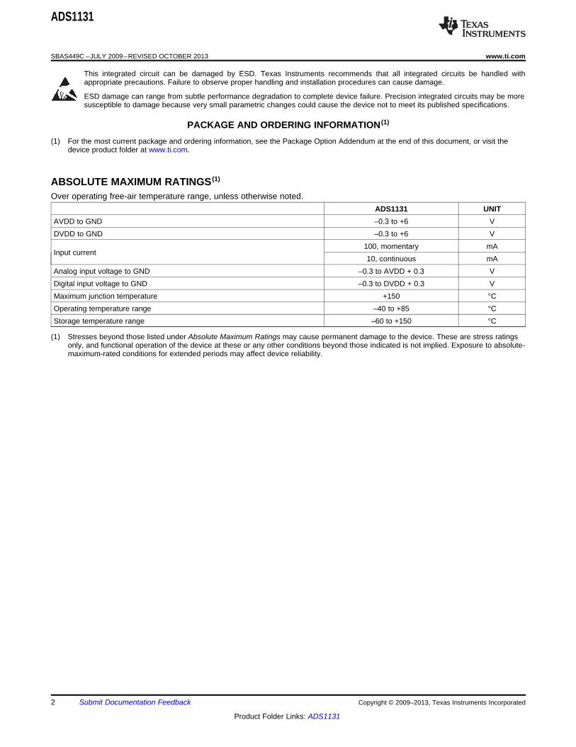
ABSOLUTE MAXIMUM RATINGS (1)
Over operating free-air temperature range, unless otherwise noted.ADS1131 UNIT
AVDD to GND –0.3 to +6 VDVDD to GND –0.3 to +6 V
100, momentary mAInput current
10, continuous mAAnalog input voltage to GND –0.3 to AVDD + 0.3 VDigital input voltage to GND –0.3 to DVDD + 0.3 VMaximum junction temperature +150 °COperating temperature range –40 to +85 °CStorage temperature range –60 to +150 °C
(1) Stresses beyond those listed under Absolute Maximum Ratings may cause permanent damage to the device. These are stress ratingsonly, and functional operation of the device at these or any other conditions beyond those indicated is not implied. Exposure to absolute-maximum-rated conditions for extended periods may affect device reliability.
2 Submit Documentation Feedback Copyright © 2009–2013, Texas Instruments Incorporated
Product Folder Links: ADS1131
ADS1131
www.ti.com SBAS449C –JULY 2009–REVISED OCTOBER 2013
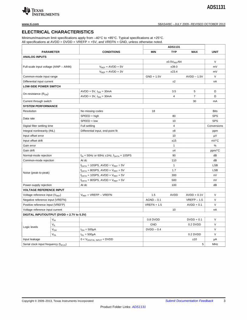
ELECTRICAL CHARACTERISTICSMinimum/maximum limit specifications apply from –40°C to +85°C. Typical specifications at +25°C.All specifications at AVDD = DVDD = VREFP = +5V, and VREFN = GND, unless otherwise noted.
ADS1131
PARAMETER CONDITIONS MIN TYP MAX UNIT
ANALOG INPUTS
±0.5VREF/64 V
Full-scale input voltage (AINP – AINN) VREF = AVDD = 5V ±39.0 mV
VREF = AVDD = 3V ±23.4 mV
Common-mode input range GND + 1.5V AVDD – 1.5V V
Differential input current ±2 nA
LOW-SIDE POWER SWITCH
AVDD = 5V, ISW = 30mA 3.5 5 ΩOn-resistance (RON)
AVDD = 3V, ISW = 30mA 4 7 Ω
Current through switch 30 mA
SYSTEM PERFORMANCE
Resolution No missing codes 18 Bits
SPEED = high 80 SPSData rate
SPEED = low 10 SPS
Digital filter settling time Full settling 4 Conversions
Integral nonlinearity (INL) Differential input, end-point fit ±8 ppm
Input offset error 10 μV
Input offset drift ±15 nV/°C
Gain error 1 %
Gain drift ±4 ppm/°C
Normal-mode rejection fIN = 50Hz or 60Hz ±1Hz, fDATA = 10SPS 90 dB
Common-mode rejection At dc 110 dB
fDATA = 10SPS, AVDD = VREF = 5V 1 LSB
fDATA = 80SPS, AVDD = VREF = 5V 1.7 LSBNoise (peak-to-peak)
fDATA = 10SPS, AVDD = VREF = 5V 300 nV
fDATA = 80SPS, AVDD = VREF = 5V 500 nV
Power-supply rejection At dc 100 dB
VOLTAGE REFERENCE INPUT
Voltage reference input (VREF) VREF = VREFP – VREFN 1.5 AVDD AVDD + 0.1V V
Negative reference input (VREFN) AGND – 0.1 VREFP – 1.5 V
Positive reference input (VREFP) VREFN + 1.5 AVDD + 0.1 V
Voltage reference input current 10 nA
DIGITAL INPUT/OUTPUT (DVDD = 2.7V to 5.3V)
VIH 0.8 DVDD DVDD + 0.1 V
VIL GND 0.2 DVDD VLogic levels
VOH IOH = 500μA DVDD – 0.4 V
VOL IOL = 500μA 0.2 DVDD V
Input leakage 0 < VDIGITAL INPUT < DVDD ±10 μA
Serial clock input frequency (fSCLK) 5 MHz
Copyright © 2009–2013, Texas Instruments Incorporated Submit Documentation Feedback 3
Product Folder Links: ADS1131
ADS1131
SBAS449C –JULY 2009–REVISED OCTOBER 2013 www.ti.com
ELECTRICAL CHARACTERISTICS (continued)Minimum/maximum limit specifications apply from –40°C to +85°C. Typical specifications at +25°C.All specifications at AVDD = DVDD = VREFP = +5V, and VREFN = GND, unless otherwise noted.
ADS1131
PARAMETER CONDITIONS MIN TYP MAX UNIT
POWER SUPPLY
Power-supply voltage (AVDD, DVDD) 3 5.3 V
Normal mode, AVDD = 3V 900 μA
Normal mode, AVDD = 5V 900 μAAnalog supply current
Standby mode 0.1 μA
Power-down 0.1 μA
Normal mode, DVDD = 3V 60 μA
Normal mode, DVDD = 5V 95 μA
Digital supply current Standby mode, SCLK = high, DVDD = 3V 45 μA
Standby mode, SCLK = high, DVDD = 5V 65 μA
Power-down 0.2 μA
Normal mode, AVDD = DVDD = 3V 2.9 mWPower dissipation, total
Normal mode, AVDD = DVDD = 5V 5.0 mW
TEMPERATURE
Operating temperature range –40 +85 °C
Specified temperature range –40 +85 °C
THERMAL INFORMATIONADS1131D
THERMAL METRIC (1) D UNITS16 PINS
θJA Junction-to-ambient thermal resistance 133.8θJC(top) Junction-to-case(top) thermal resistance 71.4θJB Junction-to-board thermal resistance 60.0
°C/WψJT Junction-to-top characterization parameter 17.4ψJB Junction-to-board characterization parameter 53.3θJC(bottom) Junction-to-case(bottom) thermal resistance n/a
(1) For more information about traditional and new thermal metrics, see the IC Package Thermal Metrics application report, SPRA953.
4 Submit Documentation Feedback Copyright © 2009–2013, Texas Instruments Incorporated
Product Folder Links: ADS1131
DVDD
GND
GND
SPEED
CAP
CAP
AINP
AINN
DRDY/DOUT
SCLK
PDWN
AVDD
SW
GND
VREFP
VREFN
1
2
3
4
5
6
7
8
16
15
14
13
12
11
10
9
ADS1131
www.ti.com SBAS449C –JULY 2009–REVISED OCTOBER 2013
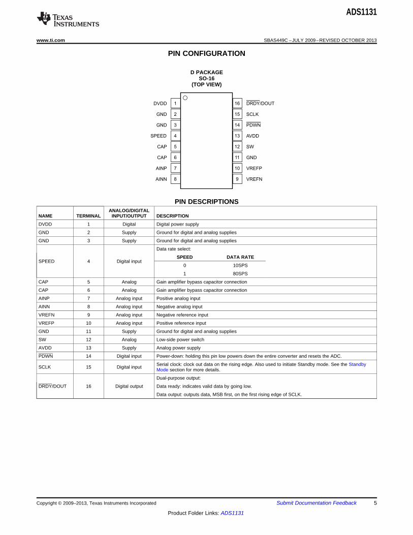
PIN CONFIGURATION
D PACKAGESO-16
(TOP VIEW)
PIN DESCRIPTIONSANALOG/DIGITAL
NAME TERMINAL INPUT/OUTPUT DESCRIPTION
DVDD 1 Digital Digital power supply
GND 2 Supply Ground for digital and analog supplies
GND 3 Supply Ground for digital and analog supplies
Data rate select:
SPEED DATA RATESPEED 4 Digital input
0 10SPS
1 80SPS
CAP 5 Analog Gain amplifier bypass capacitor connection
CAP 6 Analog Gain amplifier bypass capacitor connection
AINP 7 Analog input Positive analog input
AINN 8 Analog input Negative analog input
VREFN 9 Analog input Negative reference input
VREFP 10 Analog input Positive reference input
GND 11 Supply Ground for digital and analog supplies
SW 12 Analog Low-side power switch
AVDD 13 Supply Analog power supply
PDWN 14 Digital input Power-down: holding this pin low powers down the entire converter and resets the ADC.
Serial clock: clock out data on the rising edge. Also used to initiate Standby mode. See the StandbySCLK 15 Digital input Mode section for more details.
Dual-purpose output:
DRDY/DOUT 16 Digital output Data ready: indicates valid data by going low.
Data output: outputs data, MSB first, on the first rising edge of SCLK.
Copyright © 2009–2013, Texas Instruments Incorporated Submit Documentation Feedback 5
Product Folder Links: ADS1131
RINT
RINT
RF1
R1
RF2ADCA3
Gain = 1
CAP
AINP
CAP
A2
A1
450W
18pF
AINN
450W
18pF
ADS1131
SBAS449C –JULY 2009–REVISED OCTOBER 2013 www.ti.com
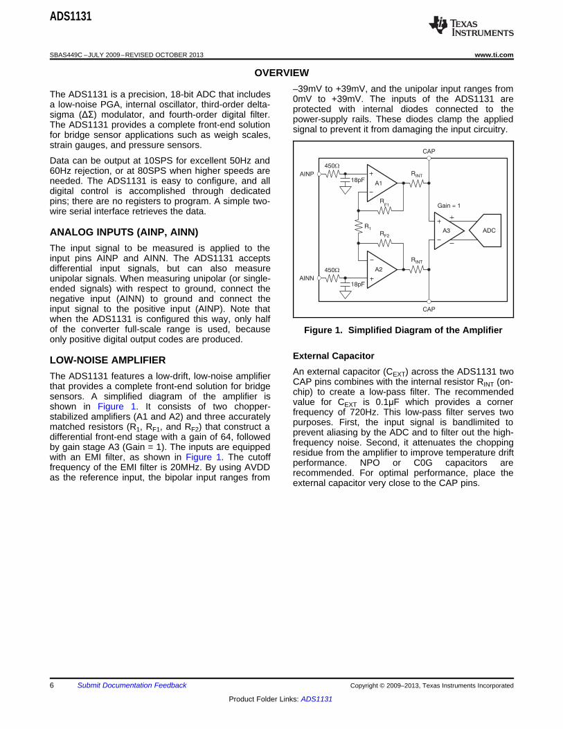
OVERVIEW–39mV to +39mV, and the unipolar input ranges fromThe ADS1131 is a precision, 18-bit ADC that includes 0mV to +39mV. The inputs of the ADS1131 area low-noise PGA, internal oscillator, third-order delta- protected with internal diodes connected to thesigma (ΔΣ) modulator, and fourth-order digital filter. power-supply rails. These diodes clamp the appliedThe ADS1131 provides a complete front-end solution signal to prevent it from damaging the input circuitry.for bridge sensor applications such as weigh scales,
strain gauges, and pressure sensors.
Data can be output at 10SPS for excellent 50Hz and60Hz rejection, or at 80SPS when higher speeds areneeded. The ADS1131 is easy to configure, and alldigital control is accomplished through dedicatedpins; there are no registers to program. A simple two-wire serial interface retrieves the data.
ANALOG INPUTS (AINP, AINN)The input signal to be measured is applied to theinput pins AINP and AINN. The ADS1131 acceptsdifferential input signals, but can also measureunipolar signals. When measuring unipolar (or single-ended signals) with respect to ground, connect thenegative input (AINN) to ground and connect theinput signal to the positive input (AINP). Note thatwhen the ADS1131 is configured this way, only halfof the converter full-scale range is used, because Figure 1. Simplified Diagram of the Amplifieronly positive digital output codes are produced.
External CapacitorLOW-NOISE AMPLIFIERAn external capacitor (CEXT) across the ADS1131 twoThe ADS1131 features a low-drift, low-noise amplifier CAP pins combines with the internal resistor RINT (on-that provides a complete front-end solution for bridge chip) to create a low-pass filter. The recommendedsensors. A simplified diagram of the amplifier is value for CEXT is 0.1μF which provides a cornershown in Figure 1. It consists of two chopper- frequency of 720Hz. This low-pass filter serves twostabilized amplifiers (A1 and A2) and three accurately purposes. First, the input signal is bandlimited tomatched resistors (R1, RF1, and RF2) that construct a prevent aliasing by the ADC and to filter out the high-differential front-end stage with a gain of 64, followed frequency noise. Second, it attenuates the choppingby gain stage A3 (Gain = 1). The inputs are equipped residue from the amplifier to improve temperature driftwith an EMI filter, as shown in Figure 1. The cutoff performance. NPO or C0G capacitors arefrequency of the EMI filter is 20MHz. By using AVDD recommended. For optimal performance, place theas the reference input, the bipolar input ranges from external capacitor very close to the CAP pins.
6 Submit Documentation Feedback Copyright © 2009–2013, Texas Instruments Incorporated
Product Folder Links: ADS1131
Bridge
Sensor
+VDD
AINP
AINN
VREFN
SW
GND
ADS1131
VREFP
AVDD
Z = 500MWEFF
VREFP VREFN
AVDD
ESD
Protection
CBUF
Z = 500MWEFF
ADS1131
www.ti.com SBAS449C –JULY 2009–REVISED OCTOBER 2013
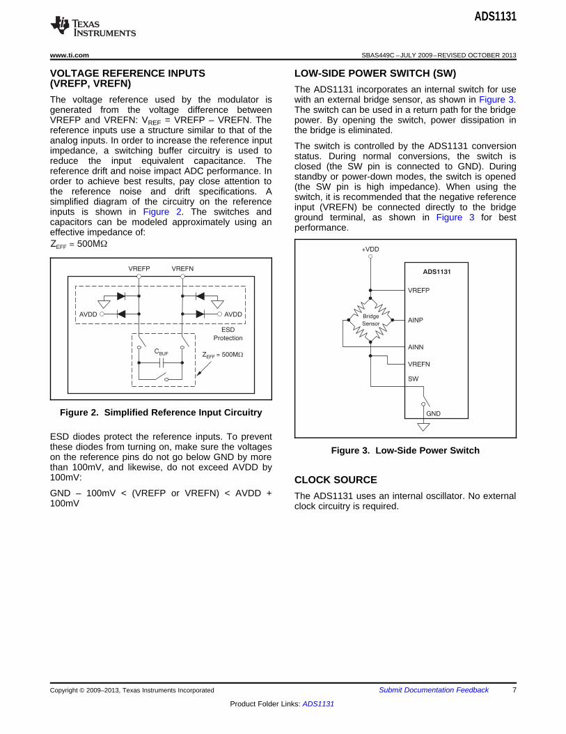
VOLTAGE REFERENCE INPUTS LOW-SIDE POWER SWITCH (SW)(VREFP, VREFN) The ADS1131 incorporates an internal switch for useThe voltage reference used by the modulator is with an external bridge sensor, as shown in Figure 3.generated from the voltage difference between The switch can be used in a return path for the bridgeVREFP and VREFN: VREF = VREFP – VREFN. The power. By opening the switch, power dissipation inreference inputs use a structure similar to that of the the bridge is eliminated.analog inputs. In order to increase the reference input The switch is controlled by the ADS1131 conversionimpedance, a switching buffer circuitry is used to status. During normal conversions, the switch isreduce the input equivalent capacitance. The closed (the SW pin is connected to GND). Duringreference drift and noise impact ADC performance. In standby or power-down modes, the switch is openedorder to achieve best results, pay close attention to (the SW pin is high impedance). When using thethe reference noise and drift specifications. A switch, it is recommended that the negative referencesimplified diagram of the circuitry on the reference input (VREFN) be connected directly to the bridgeinputs is shown in Figure 2. The switches and ground terminal, as shown in Figure 3 for bestcapacitors can be modeled approximately using an performance.effective impedance of:
Figure 2. Simplified Reference Input Circuitry
ESD diodes protect the reference inputs. To preventthese diodes from turning on, make sure the voltages Figure 3. Low-Side Power Switchon the reference pins do not go below GND by morethan 100mV, and likewise, do not exceed AVDD by100mV: CLOCK SOURCEGND – 100mV < (VREFP or VREFN) < AVDD + The ADS1131 uses an internal oscillator. No external100mV clock circuitry is required.
Copyright © 2009–2013, Texas Instruments Incorporated Submit Documentation Feedback 7
Product Folder Links: ADS1131
Frequency (Hz)
Gain
(dB
)
0
-50
-100
-150
0 10 20 30 40 50 60 70 80 90 100
(a)
Frequency (Hz)
(b)
Gain
(dB
)
-50
-100
-150
494846 47 50 51 52 53 54 55 56 57 58 59 60 61 62 63 64
Data Rate = 10SPS
Data Rate = 10SPS
ADS1131
SBAS449C –JULY 2009–REVISED OCTOBER 2013 www.ti.com
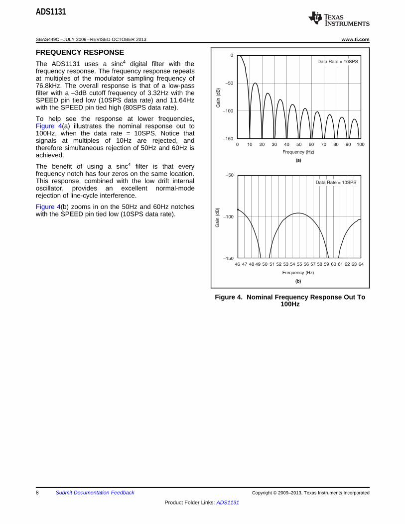
FREQUENCY RESPONSEThe ADS1131 uses a sinc4 digital filter with thefrequency response. The frequency response repeatsat multiples of the modulator sampling frequency of76.8kHz. The overall response is that of a low-passfilter with a –3dB cutoff frequency of 3.32Hz with theSPEED pin tied low (10SPS data rate) and 11.64Hzwith the SPEED pin tied high (80SPS data rate).
To help see the response at lower frequencies,Figure 4(a) illustrates the nominal response out to100Hz, when the data rate = 10SPS. Notice thatsignals at multiples of 10Hz are rejected, andtherefore simultaneous rejection of 50Hz and 60Hz isachieved.
The benefit of using a sinc4 filter is that everyfrequency notch has four zeros on the same location.This response, combined with the low drift internaloscillator, provides an excellent normal-moderejection of line-cycle interference.
Figure 4(b) zooms in on the 50Hz and 60Hz notcheswith the SPEED pin tied low (10SPS data rate).
Figure 4. Nominal Frequency Response Out To100Hz
8 Submit Documentation Feedback Copyright © 2009–2013, Texas Instruments Incorporated
Product Folder Links: ADS1131
Abrupt Change in VIN
VIN
DRDY/DOUT
Start of
Conversion
1st Conversion;
includes
unsettled V .IN
2nd Conversion;
V settled, butIN
digital filter
unsettled.
3rd Conversion;
V settled, butIN
digital filter
unsettled.
4th Conversion;
V settled, butIN
digital filter
unsettled.
5th Conversion;
V and digitalIN
filter both
settled.
Conversion
Time
ADS1131
www.ti.com SBAS449C –JULY 2009–REVISED OCTOBER 2013
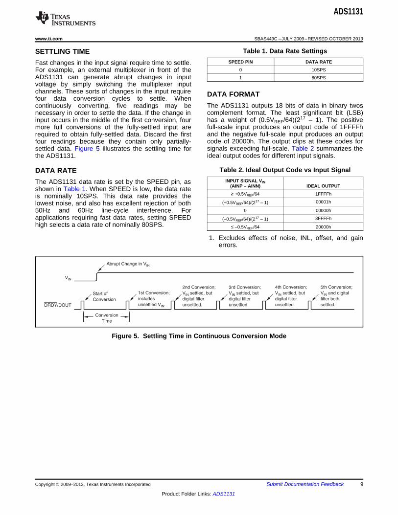
Table 1. Data Rate SettingsSETTLING TIMESPEED PIN DATA RATEFast changes in the input signal require time to settle.
0 10SPSFor example, an external multiplexer in front of theADS1131 can generate abrupt changes in input 1 80SPSvoltage by simply switching the multiplexer inputchannels. These sorts of changes in the input require DATA FORMATfour data conversion cycles to settle. When
The ADS1131 outputs 18 bits of data in binary twoscontinuously converting, five readings may becomplement format. The least significant bit (LSB)necessary in order to settle the data. If the change inhas a weight of (0.5VREF/64)(217 – 1). The positiveinput occurs in the middle of the first conversion, fourfull-scale input produces an output code of 1FFFFhmore full conversions of the fully-settled input areand the negative full-scale input produces an outputrequired to obtain fully-settled data. Discard the firstcode of 20000h. The output clips at these codes forfour readings because they contain only partially-signals exceeding full-scale. Table 2 summarizes thesettled data. Figure 5 illustrates the settling time forideal output codes for different input signals.the ADS1131.
Table 2. Ideal Output Code vs Input SignalDATA RATEINPUT SIGNAL VINThe ADS1131 data rate is set by the SPEED pin, as
(AINP – AINN) IDEAL OUTPUTshown in Table 1. When SPEED is low, the data rate≥ +0.5VREF/64 1FFFFhis nominally 10SPS. This data rate provides the
00001h(+0.5VREF/64)/(217 – 1)lowest noise, and also has excellent rejection of both0 00000h50Hz and 60Hz line-cycle interference. For
applications requiring fast data rates, setting SPEED 3FFFFh(–0.5VREF/64)/(217 – 1)high selects a data rate of nominally 80SPS. ≤ –0.5VREF/64 20000h
1. Excludes effects of noise, INL, offset, and gainerrors.
Figure 5. Settling Time in Continuous Conversion Mode
Copyright © 2009–2013, Texas Instruments Incorporated Submit Documentation Feedback 9
Product Folder Links: ADS1131
DRDY/DOUT 17 16 15
1 18
0
LSBMSB
Data
Data Ready
SCLK
tDS
tCONV
tSCLK
tPD
New Data Ready
tSCLK
tHT
tUPDATE
ADS1131
SBAS449C –JULY 2009–REVISED OCTOBER 2013 www.ti.com
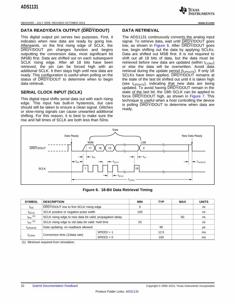
DATA READY/DATA OUTPUT (DRDY/DOUT) DATA RETRIEVALThis digital output pin serves two purposes. First, it The ADS1131 continuously converts the analog inputindicates when new data are ready by going low. signal. To retrieve data, wait until DRDY/DOUT goesAfterwards, on the first rising edge of SCLK, the low, as shown in Figure 6. After DRDY/DOUT goesDRDY/DOUT pin changes function and begins low, begin shifting out the data by applying SCLKs.outputting the conversion data, most significant bit Data are shifted out MSB first. It is not required to(MSB) first. Data are shifted out on each subsequent shift out all 18 bits of data, but the data must beSCLK rising edge. After all 18 bits have been retrieved before new data are updated (within tCONV)retrieved, the pin can be forced high with an or else the data will be overwritten. Avoid dataadditional SCLK. It then stays high until new data are retrieval during the update period (tUPDATE). If only 18ready. This configuration is useful when polling on the SCLKs have been applied, DRDY/DOUT remains atstatus of DRDY/DOUT to determine when to begin the state of the last bit shifted out until it is taken highdata retrieval. (see tUPDATE), indicating that new data are being
updated. To avoid having DRDY/DOUT remain in thestate of the last bit, the 19th SCLK can be applied toSERIAL CLOCK INPUT (SCLK)force DRDY/DOUT high, as shown in Figure 7. This
This digital input shifts serial data out with each rising technique is useful when a host controlling the deviceedge. This input has built-in hysteresis, but care is polling DRDY/DOUT to determine when data areshould still be taken to ensure a clean signal. Glitches ready.or slow-rising signals can cause unwanted additionalshifting. For this reason, it is best to make sure therise and fall times of SCLK are both less than 50ns.
Figure 6. 18-Bit Data Retrieval Timing
SYMBOL DESCRIPTION MIN TYP MAX UNITStDS DRDY/DOUT low to first SCLK rising edge 0 ns
tSCLK SCLK positive or negative pulse width 100 nstPD
(1) SCLK rising edge to new data bit valid: propagation delay 50 nstHT
(1) SCLK rising edge to old data bit valid: hold time 20 nstUPDATE Data updating: no readback allowed 90 μs
SPEED = 1 12.5 mstCONV Conversion time (1/data rate)
SPEED = 0 100 ms(1) Minimum required from simulation.
10 Submit Documentation Feedback Copyright © 2009–2013, Texas Instruments Incorporated
Product Folder Links: ADS1131

DRDY/DOUT 17 16 15
1 18
0 17
SCLK
Standby ModeData Ready
tDSS tSTANDBY tS_RDY
Start Conversion
17
1 18 19
16 15 0
Data
19th SCLK to Force /DOUT HighDRDY
Data Ready New Data Ready
DRDY/DOUT
SCLK
ADS1131
www.ti.com SBAS449C –JULY 2009–REVISED OCTOBER 2013
STANDBY MODE When tSTANDBY has passed with SCLK held high,Standby mode dramatically reduces power Standby mode activates. DRDY/DOUT stays highconsumption by shutting down most of the circuitry. In when Standby mode begins. SCLK must remain highStandby mode, the entire analog circuitry is powered to stay in Standby mode. To exit Standby modedown and only the clock source circuitry is awake to (wakeup), set SCLK low. The first data after exitingreduce the wake-up time from the Standby mode. To Standby mode are valid.enter Standby mode, simply hold SCLK high afterDRDY/DOUT goes low; see Figure 8. Standby modecan be initiated at any time during readback; it is notnecessary to retrieve all 18 bits of data beforehand.
Figure 7. Data Retrieval with DRDY/DOUT Forced High Afterwards
Figure 8. Standby Mode Timing (Can be used for single conversions)
SYMBOL DESCRIPTION MIN TYP MAX UNITSSCLK high after DRDY/DOUT SPEED = 1 12.44 ms
tDSS(1) goes low to activate Standby
SPEED = 0 99.94 msmodeSPEED = 1 0.0125 s
tSTANDBY Standby mode activation timeSPEED = 0 0.1 sSPEED = 1 No change (typical time required) msData ready after exiting StandbytS_RDY
(1)mode SPEED = 0 401.8 ms
(1) Based on an ideal internal oscillator.
Copyright © 2009–2013, Texas Instruments Incorporated Submit Documentation Feedback 11
Product Folder Links: ADS1131
Data Ready
Start
Conversion
DRDY/DOUT
SCLK
CLK Source
Wakeup
Power-Down Mode
PDWN
tWAKEUP tTS_RDY
tPDWN
ADS1131
SBAS449C –JULY 2009–REVISED OCTOBER 2013 www.ti.com
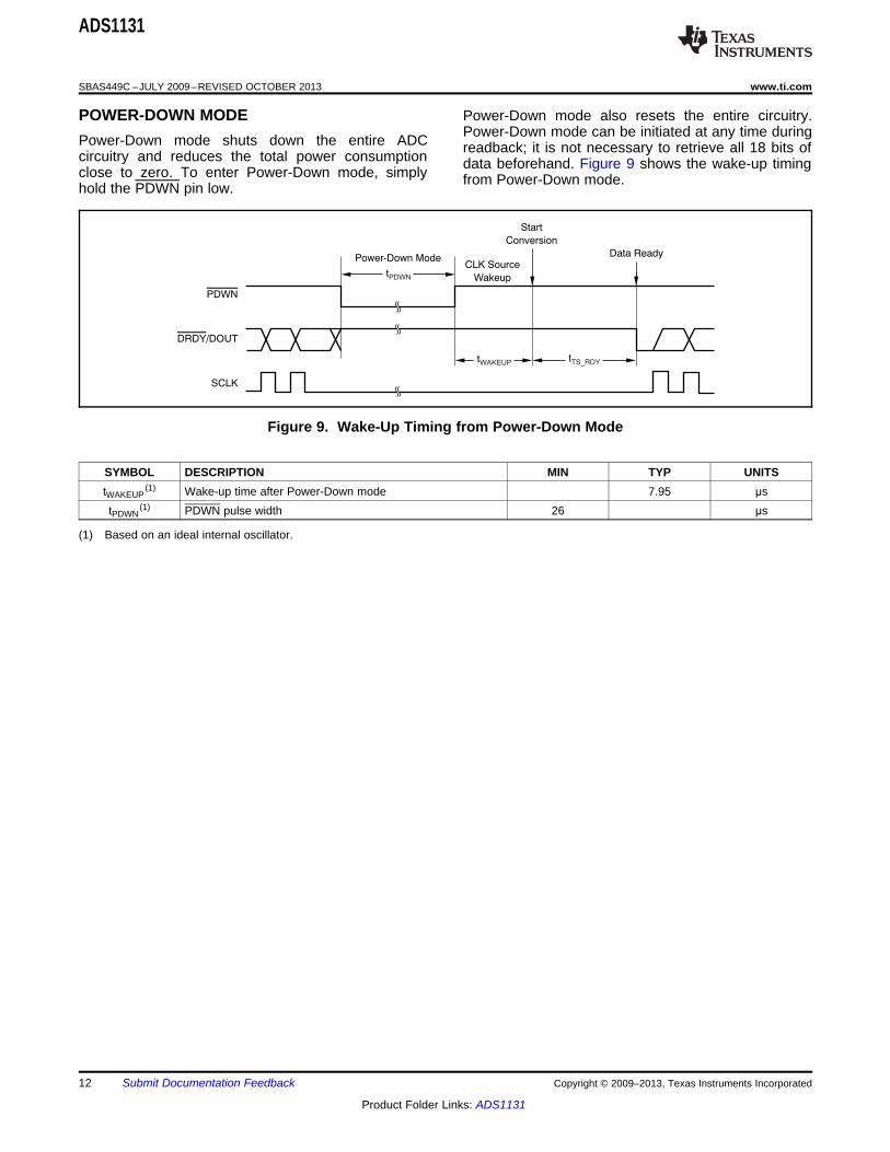
POWER-DOWN MODE Power-Down mode also resets the entire circuitry.Power-Down mode can be initiated at any time duringPower-Down mode shuts down the entire ADC readback; it is not necessary to retrieve all 18 bits ofcircuitry and reduces the total power consumption data beforehand. Figure 9 shows the wake-up timingclose to zero. To enter Power-Down mode, simply from Power-Down mode.hold the PDWN pin low.
Figure 9. Wake-Up Timing from Power-Down Mode
SYMBOL DESCRIPTION MIN TYP UNITStWAKEUP
(1) Wake-up time after Power-Down mode 7.95 μstPDWN
(1) PDWN pulse width 26 μs
(1) Based on an ideal internal oscillator.
12 Submit Documentation Feedback Copyright © 2009–2013, Texas Instruments Incorporated
Product Folder Links: ADS1131

ADS1131
10
5
6
7
8
12
16
15
14
4
VREFP
CAP
CAP
AINP
AINN
SW
AVDD DVDD
GND
DRDY/DOUT
SCLK
PDWN
SPEED
1 Fm(1)
0.1 Fm(2)
+-
2, 3, 11
13 1
MSP430x4xx
or Other
Microprocessor
VDD
GND
2.7V to 5.3V 3V
1 Fm(1)
9VREFN
LoadCell
ADS1131
www.ti.com SBAS449C –JULY 2009–REVISED OCTOBER 2013
APPLICATION EXAMPLE
Weigh Scale SystemFigure 10 shows a typical ADS1131 application as part of a weigh scale system.
(1) Place a 0.1μF or higher capacitor as close as possible on both AVDD and DVDD.(2) Place capacitor very close to the ADS1131 CAP pins for optimal performance.
Figure 10. Weigh Scale Example
Copyright © 2009–2013, Texas Instruments Incorporated Submit Documentation Feedback 13
Product Folder Links: ADS1131

ADS1131
SBAS449C –JULY 2009–REVISED OCTOBER 2013 www.ti.com
REVISION HISTORYNOTE: Page numbers for previous revisions may differ from page numbers in the current version.
Changes from Revision B (September 2011) to Revision C Page
• Changed pin 12 name from PSW to SW in pinout drawing ................................................................................................. 5• Changed pin 12 name from PSW to SW in Pin Descriptions table ...................................................................................... 5• Changed pin numbers in Figure 10 to match the device pinout ......................................................................................... 13
Changes from Revision A (May 2010) to Revision B Page
• Changed Supply Range Features bullet ............................................................................................................................... 1• Deleted ESD Ratings row and footnote 2 from Absolute Maximum Ratings table ............................................................... 2• Changed Digital Input/Output, VIH Logic level parameter minimum specification in Electrical Characteristics table ........... 3• Changed Power Supply, Power-supply voltage parameter minimum specification in Electrical Characteristics table ........ 4• Deleted Power Supply, Analog supply current parameter maximum specifications in Electrical Characteristics table ....... 4• Deleted Power Supply, Digital supply current parameter maximum specifications in Electrical Characteristics table ........ 4• Deleted Power Supply, Power dissipation parameter maximum specifications in Electrical Characteristics table .............. 4• Deleted minimum specification and added typical specification to tUPDATE row of table corresponding to Figure 6 ........... 10• Deleted Power-Up Sequence section ................................................................................................................................. 12
14 Submit Documentation Feedback Copyright © 2009–2013, Texas Instruments Incorporated
Product Folder Links: ADS1131
PACKAGE OPTION ADDENDUM
www.ti.com 9-Oct-2013
Addendum-Page 1
PACKAGING INFORMATION
Orderable Device Status(1)
Package Type PackageDrawing
Pins PackageQty
Eco Plan(2)
Lead/Ball Finish MSL Peak Temp(3)
Op Temp (°C) Device Marking(4/5)
Samples
ADS1131ID ACTIVE SOIC D 16 40 Green (RoHS& no Sb/Br)
CU NIPDAU Level-2-260C-1 YEAR -40 to 85 ADS1131
ADS1131IDR ACTIVE SOIC D 16 2500 Green (RoHS& no Sb/Br)
CU NIPDAU Level-2-260C-1 YEAR -40 to 85 ADS1131
(1) The marketing status values are defined as follows:ACTIVE: Product device recommended for new designs.LIFEBUY: TI has announced that the device will be discontinued, and a lifetime-buy period is in effect.NRND: Not recommended for new designs. Device is in production to support existing customers, but TI does not recommend using this part in a new design.PREVIEW: Device has been announced but is not in production. Samples may or may not be available.OBSOLETE: TI has discontinued the production of the device.
(2) Eco Plan - The planned eco-friendly classification: Pb-Free (RoHS), Pb-Free (RoHS Exempt), or Green (RoHS & no Sb/Br) - please check http://www.ti.com/productcontent for the latest availabilityinformation and additional product content details.TBD: The Pb-Free/Green conversion plan has not been defined.Pb-Free (RoHS): TI's terms "Lead-Free" or "Pb-Free" mean semiconductor products that are compatible with the current RoHS requirements for all 6 substances, including the requirement thatlead not exceed 0.1% by weight in homogeneous materials. Where designed to be soldered at high temperatures, TI Pb-Free products are suitable for use in specified lead-free processes.Pb-Free (RoHS Exempt): This component has a RoHS exemption for either 1) lead-based flip-chip solder bumps used between the die and package, or 2) lead-based die adhesive used betweenthe die and leadframe. The component is otherwise considered Pb-Free (RoHS compatible) as defined above.Green (RoHS & no Sb/Br): TI defines "Green" to mean Pb-Free (RoHS compatible), and free of Bromine (Br) and Antimony (Sb) based flame retardants (Br or Sb do not exceed 0.1% by weightin homogeneous material)
(3) MSL, Peak Temp. -- The Moisture Sensitivity Level rating according to the JEDEC industry standard classifications, and peak solder temperature.
(4) There may be additional marking, which relates to the logo, the lot trace code information, or the environmental category on the device.
(5) Multiple Device Markings will be inside parentheses. Only one Device Marking contained in parentheses and separated by a "~" will appear on a device. If a line is indented then it is a continuationof the previous line and the two combined represent the entire Device Marking for that device.
Important Information and Disclaimer:The information provided on this page represents TI's knowledge and belief as of the date that it is provided. TI bases its knowledge and belief on informationprovided by third parties, and makes no representation or warranty as to the accuracy of such information. Efforts are underway to better integrate information from third parties. TI has taken andcontinues to take reasonable steps to provide representative and accurate information but may not have conducted destructive testing or chemical analysis on incoming materials and chemicals.TI and TI suppliers consider certain information to be proprietary, and thus CAS numbers and other limited information may not be available for release.
In no event shall TI's liability arising out of such information exceed the total purchase price of the TI part(s) at issue in this document sold by TI to Customer on an annual basis.
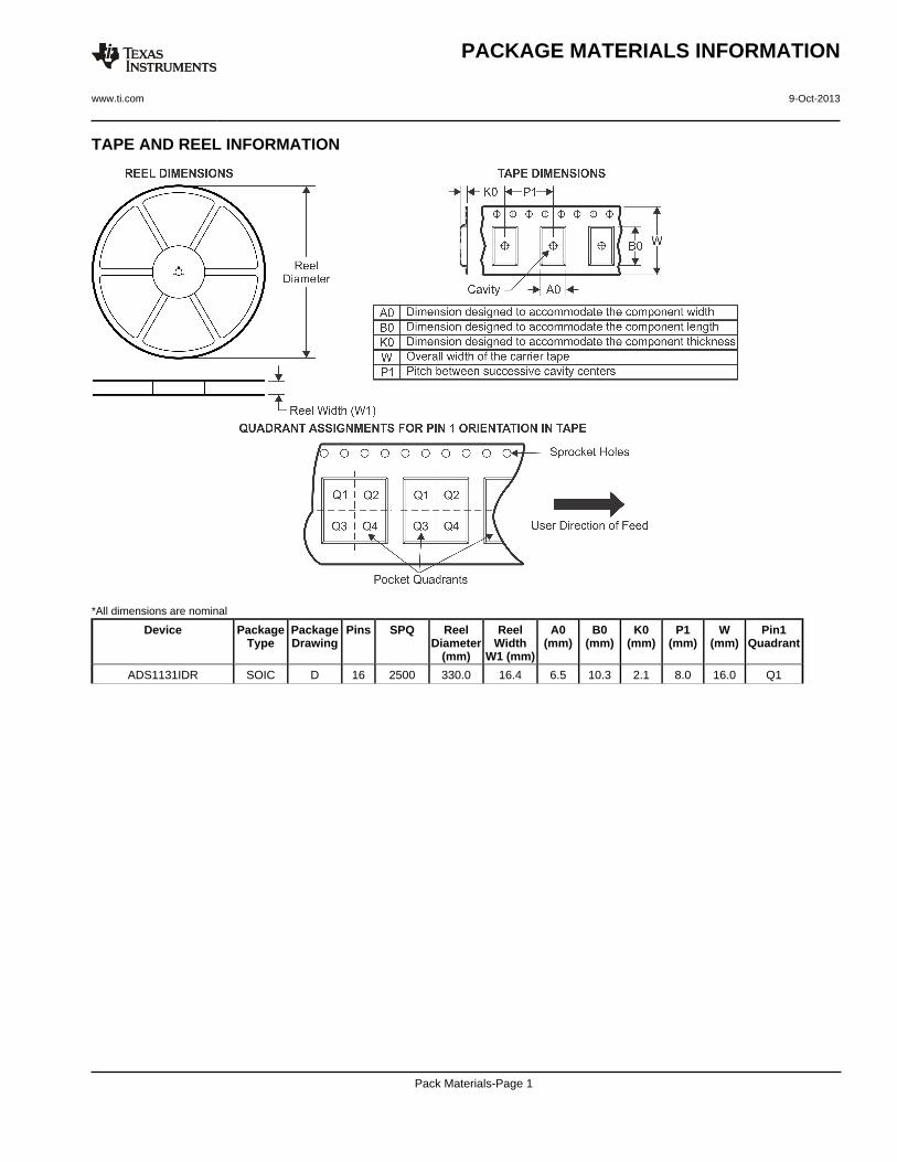
TAPE AND REEL INFORMATION
*All dimensions are nominal
Device PackageType
PackageDrawing
Pins SPQ ReelDiameter
(mm)
ReelWidth
W1 (mm)
A0(mm)
B0(mm)
K0(mm)
P1(mm)
W(mm)
Pin1Quadrant
ADS1131IDR SOIC D 16 2500 330.0 16.4 6.5 10.3 2.1 8.0 16.0 Q1
PACKAGE MATERIALS INFORMATION
www.ti.com 9-Oct-2013
Pack Materials-Page 1

*All dimensions are nominal
Device Package Type Package Drawing Pins SPQ Length (mm) Width (mm) Height (mm)
ADS1131IDR SOIC D 16 2500 333.2 345.9 28.6
PACKAGE MATERIALS INFORMATION
www.ti.com 9-Oct-2013
Pack Materials-Page 2

IMPORTANT NOTICE
Texas Instruments Incorporated and its subsidiaries (TI) reserve the right to make corrections, enhancements, improvements and otherchanges to its semiconductor products and services per JESD46, latest issue, and to discontinue any product or service per JESD48, latestissue. Buyers should obtain the latest relevant information before placing orders and should verify that such information is current andcomplete. All semiconductor products (also referred to herein as “components”) are sold subject to TI’s terms and conditions of salesupplied at the time of order acknowledgment.
TI warrants performance of its components to the specifications applicable at the time of sale, in accordance with the warranty in TI’s termsand conditions of sale of semiconductor products. Testing and other quality control techniques are used to the extent TI deems necessaryto support this warranty. Except where mandated by applicable law, testing of all parameters of each component is not necessarilyperformed.
TI assumes no liability for applications assistance or the design of Buyers’ products. Buyers are responsible for their products andapplications using TI components. To minimize the risks associated with Buyers’ products and applications, Buyers should provideadequate design and operating safeguards.
TI does not warrant or represent that any license, either express or implied, is granted under any patent right, copyright, mask work right, orother intellectual property right relating to any combination, machine, or process in which TI components or services are used. Informationpublished by TI regarding third-party products or services does not constitute a license to use such products or services or a warranty orendorsement thereof. Use of such information may require a license from a third party under the patents or other intellectual property of thethird party, or a license from TI under the patents or other intellectual property of TI.
Reproduction of significant portions of TI information in TI data books or data sheets is permissible only if reproduction is without alterationand is accompanied by all associated warranties, conditions, limitations, and notices. TI is not responsible or liable for such altereddocumentation. Information of third parties may be subject to additional restrictions.
Resale of TI components or services with statements different from or beyond the parameters stated by TI for that component or servicevoids all express and any implied warranties for the associated TI component or service and is an unfair and deceptive business practice.TI is not responsible or liable for any such statements.
Buyer acknowledges and agrees that it is solely responsible for compliance with all legal, regulatory and safety-related requirementsconcerning its products, and any use of TI components in its applications, notwithstanding any applications-related information or supportthat may be provided by TI. Buyer represents and agrees that it has all the necessary expertise to create and implement safeguards whichanticipate dangerous consequences of failures, monitor failures and their consequences, lessen the likelihood of failures that might causeharm and take appropriate remedial actions. Buyer will fully indemnify TI and its representatives against any damages arising out of the useof any TI components in safety-critical applications.
In some cases, TI components may be promoted specifically to facilitate safety-related applications. With such components, TI’s goal is tohelp enable customers to design and create their own end-product solutions that meet applicable functional safety standards andrequirements. Nonetheless, such components are subject to these terms.
No TI components are authorized for use in FDA Class III (or similar life-critical medical equipment) unless authorized officers of the partieshave executed a special agreement specifically governing such use.
Only those TI components which TI has specifically designated as military grade or “enhanced plastic” are designed and intended for use inmilitary/aerospace applications or environments. Buyer acknowledges and agrees that any military or aerospace use of TI componentswhich have not been so designated is solely at the Buyer's risk, and that Buyer is solely responsible for compliance with all legal andregulatory requirements in connection with such use.
TI has specifically designated certain components as meeting ISO/TS16949 requirements, mainly for automotive use. In any case of use ofnon-designated products, TI will not be responsible for any failure to meet ISO/TS16949.
Products Applications
Audio www.ti.com/audio Automotive and Transportation www.ti.com/automotive
Amplifiers amplifier.ti.com Communications and Telecom www.ti.com/communications
Data Converters dataconverter.ti.com Computers and Peripherals www.ti.com/computers
DLP® Products www.dlp.com Consumer Electronics www.ti.com/consumer-apps
DSP dsp.ti.com Energy and Lighting www.ti.com/energy
Clocks and Timers www.ti.com/clocks Industrial www.ti.com/industrial
Interface interface.ti.com Medical www.ti.com/medical
Logic logic.ti.com Security www.ti.com/security
Power Mgmt power.ti.com Space, Avionics and Defense www.ti.com/space-avionics-defense
Microcontrollers microcontroller.ti.com Video and Imaging www.ti.com/video
RFID www.ti-rfid.com
OMAP Applications Processors www.ti.com/omap TI E2E Community e2e.ti.com
Wireless Connectivity www.ti.com/wirelessconnectivity
Mailing Address: Texas Instruments, Post Office Box 655303, Dallas, Texas 75265Copyright © 2013, Texas Instruments Incorporated