16mb async/page/burst cellularram 1 - integrated silicon
TRANSCRIPT

IS66WVC1M16ALL IS67WVC1M16ALL
1 Rev.A | October 2013 www.issi.com – [email protected]
Overview
The IS66WVC1M16ALL and IS67WVC1M16ALL is an integrated memory device containing 16Mbit Pseudo Static Random Access Memory using a self-refresh DRAM array organized as 1M words by 16 bits. The device includes several power saving modes : Reduced Array Refresh mode where data is retained in a portion of the array and Temperature Controlled Refresh. Both these modes reduce standby current drain. The device can be operated in a standard asynchronous mode and high performance burst mode. The die has separate power rails, VDDQ and VSSQ for the I/O to be run from a separate power supply from the device core.
Single device supports asynchronous , page,
and burst operation
Mixed Mode supports asynchronous write and
synchronous read operation
Dual voltage rails for optional performance
VDD 1.7V~1.95V, VDDQ 1.7V~1.95V
Asynchronous mode read access : 70ns
Interpage Read access : 70ns
Intrapage Read access : 20ns
Burst mode for Read and Write operation
4, 8, 16,32 or Continuous
Low Power Consumption
Asynchronous Operation < 25 mA
Intrapage Read < 18mA
Burst operation < 45 mA (@133Mhz)
Standby < 80 uA(max.)
Deep power-down (DPD) < 3uA (Typ)
Low Power Feature
Reduced Array Refresh
Temperature Controlled Refresh
Deep power-down (DPD) mode
Operation Frequency up to 133Mhz
Operating temperature Range
Industrial: -40°C~85°C
Automotive A1: -40°C~85°C
Package: 54-ball VFBGA
16Mb Async/Page/Burst CellularRAM 1.5
Features
Copyright © 2013 Integrated Silicon Solution, Inc. All rights reserved. ISSI reserves the right to make changes to this specification and its
products at any time without notice. ISSI assumes no liability arising out of the application or use of any information, products or services
described herein. Customers are advised to obtain the latest version of this device specification before relying on any published information
and before placing orders for products.
Integrated Silicon Solution, Inc. does not recommend the use of any of its products in life support applications where the failure or
malfunction of the product can reasonably be expected to cause failure of the life support system or to significantly affect its safety or
effectiveness. Products are not authorized for use in such applications unless Integrated Silicon Solution, Inc. receives written assurance to
its satisfaction, that:
a.) the risk of injury or damage has been minimized;
b.) the user assume all such risks; and
c.) potential liability of Integrated Silicon Solution, Inc is adequately protected under the circumstances

IS66WVC1M16ALL IS67WVC1M16ALL
2 Rev.A | October 2013 www.issi.com – [email protected]
General Description CellularRAM™ (Trademark of MicronTechnology Inc.) products are high-speed, CMOS pseudo-static random access memory developed for low-power, portable applications. The 16Mb DRAM core device is organized as 1 Meg x 16 bits. This device is a variation of the industry-standard Flash control interface that dramatically increase READ/WRITE bandwidth compared with other low-power SRAM or Pseudo SRAM offerings. To operate seamlessly on a burst Flash bus, CellularRAM products have incorporated a transparent self-refresh mechanism. The hidden refresh requires no additional support from the system memory controller and has no significant impact on device read/write performance. Two user-accessible control registers define device operation. The bus configuration register (BCR) defines how the CellularRAM device interacts with the system memory bus and is nearly identical to its counterpart on burst mode Flash devices. The refresh configuration register (RCR) is used to control how refresh is performed on the DRAM array. These registers are automatically loaded with default settings during power-up and can be updated anytime during normal operation. Special attention has been focused on standby current consumption during self refresh. CellularRAM products include three mechanisms to minimize standby current. Partial array refresh (PAR) enables the system to limit refresh to only that part of the DRAM array that contains essential data. Temperature-compensated refresh (TCR) uses an on-chip sensor to adjust the refresh rate to match the device temperature — the refresh rate decreases at lower temperatures to minimize current consumption during standby. Deep power-down (DPD) enables the system to halt the refresh operation altogether when no vital information is stored in the device. The system-configurable refresh mechanisms are adjusted through the RCR. This CellularRAM device is compliant with the industry-standard CellularRAM 1.5 feature set established by the CellularRAM Workgroup. It includes support for both variable and fixed latency, with three drive strengths, a variety of wrap options, and a device ID register (DIDR).
[ Functional Block Diagram]
Address Decode Logic
Refresh Configuration Register
(RCR)
Bus Configuration Register
(BCR)
1024K X 16 DRAM
Memory Array
Input /Output
Mux And
Buffers
DQ0~DQ15
A0~A19
Device ID Register (DIDR)
Control Logic
CE# WE# OE# CLK
ADV# CRE LB# UB#
WAIT

IS66WVC1M16ALL IS67WVC1M16ALL
3 Rev.A | October 2013 www.issi.com – [email protected]
54Ball VFBGA Ball Assignment
[Top View] (Ball Down)

IS66WVC1M16ALL IS67WVC1M16ALL
4 Rev.A | October 2013 www.issi.com – [email protected]
Signal Descriptions
All signals for the device are listed below in Table 1.
Symbol Type Description
VDD Power Supply Core Power supply (1.7V~1.95V)
VDDQ Power Supply I/O Power supply (1.7V~1.95V)
VSS Power Supply All VSS supply pins must be connected to Ground
VSSQ Power Supply All VSSQ supply pins must be connected to Ground
DQ0~DQ15 Input / Output Data Inputs/Outputs (DQ0~DQ15)
A0~A19 Input Address Input(A0~A19)
LB# Input Lower Byte select
UB# Input Upper Byte select
CE# Input Chip Enable/Select
OE# Input Output Enable
WE# Input Write Enable
CRE Input Control Register Enable: When CRE is HIGH, READ and WRITE operations access registers.
ADV# Input Address Valid signal
Indicates that a valid address is present on the address inputs. Address can be latched on the rising edge of ADV# during asynchronous Read and Write operations. ADV# can be held LOW during asynchronous Read and Write operations.
CLK Input Clock
Latches addresses and commands on the first rising CLK edge when ADV# is active in synchronous mode. CLK must be kept static Low during asynchronous Read/Write operations and Page Read access operations.
WAIT Output WAIT
Data valid signal during burst Read/Write operation. WAIT is used to arbitrate collisions between refresh and Read/Write operation. WAIT is also asserted at the end of a row unless wrapping within the burst length. WAIT is asserted and should be ignored during asynchronous and page mode operation. WAIT is gated by CE# and is high-Z when CE# is high.
Table 1. Signal Descriptions

IS66WVC1M16ALL IS67WVC1M16ALL
5 Rev.A | October 2013 www.issi.com – [email protected]
Functional Description
All functions for the device are listed below in Table 2.
Mode Power CLK1 ADV# CE# OE# WE# CRE2 UB#/ LB#
WAIT3 DQ
[15:0]4 Note
Asynchronous Mode
Read Active L L L L H L L Low-Z Data-out 5
Write Active L L L X L L L Low-Z Data-in 5
Standby Standby
L X H X X L X High-Z High-Z 6,7
No Operation Idle L X L X X L X Low-Z X 5,7
Configuration Register Write
Active L L L H L H X Low-Z High-Z
Configuration Register Read
Active L L L L H H L Low-Z Config-Reg Out
Deep Power-Down DPD L X H X X X X High-Z High-Z 10
Synchronous Mode (Burst Mode)
Async read Active L L L L H L L Low-Z Data-Out 5
Async write Active L L L X L L L Low-Z Data-In 5
Standby Stand
by L X H X X L X High-Z High-Z 6,7
No operation Idle L X L X X L X Low-Z X 5,8
Initial burst read
Active L L X H L L Low-Z X 5,8
Initial burst write
Active L L H L L X Low-Z X 5,8
Burst continue
Active H L X X X L Low-Z Data-In or Data-Out
5,8
Burst suspend Active X X L H X X X Low-Z High-Z 5,8
Configuration register write
Active L L H L H X Low-Z High-Z 8,11
Configuration register read
Active L L L H H L Low-Z Config-Reg
Out 8,11
Deep Power-Down
DPD L X H X X X X High-Z High-Z 10
Table 2. Functional Descriptions

IS66WVC1M16ALL IS67WVC1M16ALL
6 Rev.A | October 2013 www.issi.com – [email protected]
Notes
1. CLK must be LOW during Async Read and Async Write modes. CLK must be LOW to achieve
low standby current during standby mode and DPD modes. CLK must be static (LOW or HIGH)
during burst suspend.
2. Configuration registers are accessed when CRE is HIGH during the address portion
of a READ or WRITE cycle.
3. WAIT polarity is configured through the bus configuration register (BCR[10]).
4. When UB# and LB# are in select mode (LOW), DQ0~DQ15 are affected as shown.
When only LB# is in select mode, DQ0~DQ7 are affected as shown. When only UB# is
in select mode, DQ8~DQ15 are affected as shown.
5. The device will consume active power in this mode whenever addresses are changed
6. When the device is in standby mode, address inputs and data inputs/outputs are internally
isolated from any external influence.
7. Vin=VDDQ or 0V, all device pins be static (unswitched) in order to achieve standby current.
8. Burst mode operation is initialized through the bus configuration register (BCR[15]).
9. Byte operation can be supported Write & Read at asynchronous mode and Write at
synchronous mode.
10. DPD is initiated when CE# transition from LOW to HIGH after writing RCR[4] to 0. DPD is
maintained until CE# transitions from HIGH to LOW
11. Initial cycle. Following cycles are the same as BURST CONTINUE. CE# must stay LOW
for the equivalent of a single word burst (as indicated by WAIT).
12. When the BCR is configured for sync mode, sync READ and sync WRITE and async WRITE
are supported.

IS66WVC1M16ALL IS67WVC1M16ALL
7 Rev.A | October 2013 www.issi.com – [email protected]
Functional Description In general, this device is high-density alternatives to SRAM and Pseudo SRAM products popular in low-power, portable applications. The 16Mb device contains a 16,777,216-bit DRAM core organized as 1,048,576 addresses by 16 bits. This device implements the same high-speed bus interface found on burst mode Flash products. The CellularRAM bus interface supports both asynchronous and burst mode transfers. Page mode accesses are also included as a bandwidth-enhancing extension to the asynchronous read protocol.
Power-Up Initialization
CellularRAM products include an on-chip voltage sensor used to launch the power-up initialization process. Initialization will configure the BCR and the RCR with their default settings (see Table 3 and Table 8). VDD and VDDQ must be applied simultaneously. When they reach a stable level at or above 1.7V, the device will require 150μs to complete its self-initialization process. During the initialization period, CE# should remain HIGH. When initialization is complete, the device is ready for normal operation.
Figure 1: Power-Up Initialization Timing
VDD=1.7V
Device Initialization
tPU > 150us Device ready for
normal operation VDD
VDDQ

IS66WVC1M16ALL IS67WVC1M16ALL
8 Rev.A | October 2013 www.issi.com – [email protected]
Bus Operating Modes CellularRAM products incorporate a burst mode interface targeted at low-power, wireless applications. This bus interface supports asynchronous, page mode, and burst mode read and write transfers. The specific interface supported is defined by the value loaded into the bus configuration register. Page mode is controlled by the refresh configuration register (RCR[7]).
Burst Mode Operation
Burst mode operations enable high-speed synchronous READ and WRITE operations. Burst operations consist of a multi-clock sequence that must be performed in an ordered fashion. After CE# goes LOW, the address to access is latched on the rising edge of the next clock that ADV# is LOW. During this first clock rising edge, WE# indicates whether the operation is going to be a READ (WE#=HIGH) or WRITE(WE#=LOW). The size of a burst can be specified in the BCR either as a fixed length or continuous. Fixed-length bursts consist of four, eight, sixteen, or thirty-two words. Continuous bursts have the ability to start at a specified address and burst to the end of the row. (Row length of 128 words or 256 words is a manufacturer option.) The latency count stored in the BCR defines the number of clock cycles that elapse before the initial data value is transferred between the processor and CellularRAM device. The initial latency for READ operations can be configured as fixed or variable. (WRITE operations always use fixed latency). Variable latency allows the CellularRAM to be configured for minimum latency at high clock frequencies, but the controller must monitor WAIT to detect any conflict with refresh cycles.(see Figure 26). Fixed latency outputs the first data word after the worst-case access delay, including allowance for refresh collisions. The initial latency time and clock speed determine the latency count setting. Fixed latency is used when the controller cannot monitor WAIT. Fixed latency also provides improved performance at lower clock frequencies. The WAIT output asserts when a burst is initiated and de-asserts to indicate when data is to be transferred into (or out of) the memory. WAIT will again be asserted at the boundary of the row unless wrapping within the burst length. To access other devices on the same bus without the timing penalty of the initial latency for a new burst, burst mode can be suspended. Bursts are suspended by stopping CLK. CLK must be stopped LOW. If another device will use the data bus while the burst is suspended, OE# should be taken HIGH to disable the CellularRAM outputs; otherwise, OE# can remain LOW. Note that the WAIT output will continue to be active, and as a result no other devices should directly share the WAIT connection to the controller. To continue the burst sequence, OE# is taken LOW, then CLK is restarted after valid data is available on the bus. CE# LOW time is limited by refresh considerations. CE# must not stay LOW longer than tCEM. If a burst suspension will cause CE# to remain LOW for longer than tCEM, CE# should be taken HIGH and the burst restarted with a new CE# LOW/ADV# LOW cycle.

IS66WVC1M16ALL IS67WVC1M16ALL
9 Rev.A | October 2013 www.issi.com – [email protected]
Burst Read Operation After CE# goes LOW, the address to access is latched on the rising edge of the next clock that ADV# is LOW. During this first clock rising edge, WE# indicates whether the operation is going to be a READ (WE# = HIGH, Figure 2) Then the data needs to be output to data bus (DQ0~DQ15) according to set WAIT states. The WAIT output asserts when a burst is initiated, and de-asserts to indicate when data is to be transferred into (or out of ) the memory. WAIT will again be asserted at the boundary of a row, unless wrapping within the burst length. A full 4 word synchronous read access is shown in Figure 2 and the AC characteristics are specified in Table 16.
Figure 2. Synchronous Read Access Timing
Address
DQ0- DQ15
ADV#
CE#
UB#/LB#
WAIT
WE#
OE#
CLK
Read Burst Identified (WE#=HIGH)
tCLK
VALID ADDRESS
tSP tHD
tSP tHD tKOH tACLK
tCEM
tCSP
tHD
tSP tHD
tBOE
tOLZ
tKHTL
VALID OUTPUT
VALID OUTPUT
VALID OUTPUT
VALID OUTPUT
tCBPH
tHZ
tABA
tHZ
HiZ
tCEW
tOHZ
tSP tHD

IS66WVC1M16ALL IS67WVC1M16ALL
10 Rev.A | October 2013 www.issi.com – [email protected]
Burst Write Operation After CE# goes LOW, the address to access is latched on the rising edge of the next clock that ADV# is LOW. During this first clock rising edge, WE# indicates whether the operation is going to be a WRITE (WE# =LOW, Figure 3). Data is placed to the data bus (DQ0~DQ15) with consecutive clock cycles when WAIT de-asserts. The WAIT output asserts when a burst is initiated, and de-asserts to indicate when data is to be transferred into (or out of ) the memory. WAIT will again be asserted at the boundary of a row, unless wrapping within the burst length. A full 4 word synchronous write access is shown in Figure 3 and the AC characteristics are specified in Table 18.
Figure 3. Synchronous Write Access Timing
Write Burst Identified (WE#=LOW)
Address
DQ0- DQ15
ADV#
CE#
UB#/LB#
WAIT
WE#
CLK
tCLK
VALID ADDRESS
tCEW
tSP tHD tHD
tCEM
tCSP
tHD
tSP tHD
tKHTL
DATA IN DATA IN DATA IN DATA IN
tCBPH
HiZ
tSP
tHD
tSP
tAS
tAS
tHD

IS66WVC1M16ALL IS67WVC1M16ALL
11 Rev.A | October 2013 www.issi.com – [email protected]
Asynchronous Mode Asynchronous mode uses industry-standard SRAM control signals (CE#, OE#, WE#, UB#, and LB#). READ operations (Figure 4) are initiated by bringing CE#, OE#, UB#/LB# LOW while keeping WE# HIGH. Valid data will be driven out of the I/Os after the specified access time has elapsed. WRITE operations (Figure 5) occur when CE#, WE#, UB#/LB# are driven LOW. During asynchronous WRITE operations, the OE# level is a “Don't Care,” and WE# will override OE#. The data to be written is latched on the rising edge of CE#, WE#, UB#/LB# (whichever occurs first). Asynchronous operations (page mode disabled) can either use the ADV input to latch the address, or ADV can be driven LOW during the entire READ/WRITE operations During asynchronous operation, the CLK input must be held LOW. WAIT will be driven during asynchronous READs, and its state should be ignored. WE# must not be held LOW longer than tCEM.
Figure 4. Asynchronous Read Access Timing (ADV# LOW)
Address
DQ0- DQ15
CE#
UB#/LB#
OE#
WE#
VALID ADDRESS
VALID OUTPUT
tRC = READ cycle Time
Notes: 1. ADV must remain LOW for PAGE MODE operation.

IS66WVC1M16ALL IS67WVC1M16ALL
12 Rev.A | October 2013 www.issi.com – [email protected]
Figure 5. Asynchronous Write Access Timing (ADV# LOW)
Address
DQ0- DQ15
CE#
UB#/LB#
WE#
OE#
VALID ADDRESS
VALID OUTPUT
tWC = WRITE cycle Time
< tCEM

IS66WVC1M16ALL IS67WVC1M16ALL
13 Rev.A | October 2013 www.issi.com – [email protected]
Page Mode READ Operation Page mode is a performance-enhancing extension to the legacy asynchronous READ operation. In page-mode-capable products, an initial asynchronous read access is preformed, then adjacent addresses can be read quickly by simply changing the low-order address. Addresses A[3:0] are used to determine the members of the 16-address CellularRAM page. Any change in addresses A[4] or higher will initiate a new tAA access time. Figure 6 shows the timing for a page mode access. Page mode takes advantage of the fact that adjacent addresses can be read in a shorter period of time than random addresses. WRITE operations do not include comparable page mode functionality. During asynchronous page mode operation, the CLK input must be held LOW. CE# must be driven HIGH upon completion of a page mode access. WAIT will be driven while the device is enabled and its state should be ignored. Page mode is enabled by setting RCR[7] to HIGH. ADV must be driven LOW during all page mode READ accesses. Due to refresh considerations, CE# must not be LOW longer than tCEM.
Figure 6. Page Mode READ Operation (ADV# LOW)
Address
DQ0- DQ15
CE#
UB#/LB#
OE#
WE#
tAA
Notes: 1. ADV must remain LOW for PAGE MODE operation.
ADD3 ADD2 ADD1 ADD0
D0 D1 D2 D3
tAPA tAPA tAPA

IS66WVC1M16ALL IS67WVC1M16ALL
14 Rev.A | October 2013 www.issi.com – [email protected]
Mixed-Mode Operation The device can support a combination of synchronous READ and asynchronous READ and WRITE operations when the BCR is configured for synchronous operation. The asynchronous READ and WRITE operations require that the clock (CLK) remain LOW during the entire sequence. The ADV# signal can be used to latch the target address, or it can remain LOW during the entire WRITE operation. CE# can remain LOW when transitioning between mixed-mode operations with fixed latency enabled; however, the CE# LOW time must not exceed tCEM. Mixed-mode operation facilitates a seamless interface to legacy burst mode Flash memory controllers. See Figure 45 for the “Asynchronous WRITE Followed by Burst READ” timing diagram.
WAIT Operation
WAIT output on the CellularRAM device is typically connected to a shared, system-level WAIT signal. The shared WAIT signal is used by the processor to coordinate transactions with multiple memories on the synchronous bus. When a synchronous READ or WRITE operation has been initiated, WAIT goes active to indicate that the CellularRAM device requires additional time before data can be transferred. For READ operations, WAIT will remain active until valid data is output from the device. For WRITE operations, WAIT will indicate to the memory controller when data will be accepted into the CellularRAM device. When WAIT transitions to an inactive state, the data burst will progress on successive rising clock edges. During a burst cycle CE# must remain asserted until the first data is valid. Bringing CE# HIGH during this initial latency may cause data corruption. When using variable initial access latency (BCR[14] = 0), the WAIT output performs an arbitration role for READ operations launched while an on-chip refresh is in progress. If a collision occurs, the WAIT pin is asserted for additional clock cycles until the refresh has completed (see Figure 26). When the refresh operation has completed, the READ operation will continue normally. WAIT will be asserted but should be ignored during asynchronous READ and WRITE and page READ operations. WAIT will be High-Z during asynchronous WRITE operations. By using fixed initial latency (BCR[14] = 1), this CellularRAM device can be used in burst mode without monitoring the WAIT pin. However, WAIT can still be used to determine when valid data is available at the start of the burst and at the end of the row. If wait is not monitored, the controller must stop burst accesses at row boundaries on its own.
UB#/LB# Operation
The UB#/LB# enable signals support byte-wide data WRITEs. During WRITE operations, any disabled bytes will not be transferred to the RAM array and the internal value will remain unchanged. During an asynchronous WRITE cycle, the data to be written is latched on the rising edge of CE#, WE#, UB#, and LB# whichever occurs first. UB#/LB# must be LOW during synchronous READ cycles. When UB#/LB# are disabled (HIGH) during an operation, the device will disable the data bus from receiving or transmitting data. Although the device will seem to be deselected, it remains in an active mode as long as CE# remains LOW.

IS66WVC1M16ALL IS67WVC1M16ALL
15 Rev.A | October 2013 www.issi.com – [email protected]
Low-Power Feature Standby Mode Operation
During standby, the device current consumption is reduced to the level necessary to perform the DRAM refresh operation. Standby operation occurs when CE# is HIGH. The device will enter a reduced power state upon completion of a READ or WRITE operation, or when the address and control inputs remain static for an extended period of time. This mode will continue until a change occurs to the address or control inputs.
Temperature-Compensated Refresh
Temperature-compensated refresh (TCR) allows for adequate refresh at different temperatures. This CellularRAM device includes an on-chip temperature sensor that automatically adjusts the refresh rate according to the operating temperature. The device continually adjusts the refresh rate to match that temperature.
Partial-Array Refresh
Partial-array refresh (PAR) restricts refresh operation to a portion of the total memory array. This feature enables the device to reduce standby current by refreshing only that part of the memory array required by the host system. The refresh options are full array, one-half array, one-quarter array, one-eighth array, or none of the array. The mapping of these partitions can start at either the beginning or the end of the address map (see Table 9). READ and WRITE operations to address ranges receiving refresh will not be affected. Data stored in addresses not receiving refresh will become corrupted. When re-enabling additional portions of the array, the new portions are available immediately upon writing to the RCR.
Deep Power-Down Operation
Deep power-down (DPD) operation disables all refresh-related activity. This mode is used if the system does not require the storage provided by the CellularRAM device. Any stored data will become corrupted when DPD is enabled. When refresh activity has been re-enabled, the CellularRAM device will require 150μs to perform an initialization procedure before normal operations can resume. During this 150μs period, the current consumption will be higher than the specified standby levels, but considerably lower than the active current specification. DPD can be enabled by writing to the RCR using CRE or the software access sequence; DPD starts when CE# goes HIGH. DPD is disabled the next time CE# goes LOW and stays LOW for at least 10us.

IS66WVC1M16ALL IS67WVC1M16ALL
16 Rev.A | October 2013 www.issi.com – [email protected]
Registers Two user-accessible configuration registers define the device operation. The bus configuration register (BCR) defines how the CellularRAM interacts with the system memory bus and is nearly identical to its counterpart on burst mode Flash devices. The refresh configuration register (RCR) is used to control how refresh is performed on the DRAM array. These registers are automatically loaded with default settings during power-up, and can be updated any time the devices are operating in a standby state. A DIDR provides information on the device manufacturer, CellularRAM generation, and the specific device configuration. The DIDR is read-only.
Access Using CRE
The registers can be accessed using either a synchronous or an asynchronous operation when the configuration register enable (CRE) input is HIGH (see Figures 7 through 10). When CRE is LOW, a READ or WRITE operation will access the memory array. The configuration register values are written via A[19:0]. In an asynchronous WRITE, the values are latched into the configuration register on the rising edge of ADV#, CE#, or WE#, whichever occurs first; LB# and UB# are “Don’t Care” The BCR is accessed when A[19:18] is 10b; the RCR is accessed when A[19:18] is 00b; the DIDR is accessed when A[19:18] is 01b. For READs, address inputs other than A[19:18] are “Don’t Care,” and register bits 15:0 are output on DQ[15:0]. Immediately after performing a configuration register READ or WRITE operation, reading the memory array is highly recommended
Figure 7: Configuration Register WRITE – Asynchronous Mode, Followed by READ ARRAY Operation
Address
DQ0- DQ151
ADV#
CE#
UB#/LB#
CRE2
WE#
OE#
tVP
tAVS tAVH
OPCODE1
tCW
tVS
tWP
tCVS
tVP
tAVS tAVH
VALID ADDRESS
VALID OUTPUT
tCO
tAADV
tOE
tBA
tHZ
tCVS
tOLZ
tCPH
tAVS
Write Address Bus Value to Control
Register
tAVH
Notes: 1. A[19:18] = 00b to load RCR, and 10b to load BCR. 2. CRE must be HIGH to access registers.

IS66WVC1M16ALL IS67WVC1M16ALL
17 Rev.A | October 2013 www.issi.com – [email protected]
Figure 8: Configuration Register WRITE – Synchronous Mode Followed by READ ARRAY Operation
VALID ADDRESS
tSP tHD tKOH tACLK
tCEM
tHD
tBOE
tKHTL
VALID OUTPUT
VALID OUTPUT
VALID OUTPUT
VALID OUTPUT
tABA
tHZ
tCEW
tOHZ
Address
DQ0- DQ15
ADV#
CE#
UB#/LB#
WAIT
WE#
OE#
CLK
Notes:
1. Non-default BCR settings for configuration register WRITE in synchronous mode, followed by READ ARRAY
operation: Latency code two (three clocks); WAIT active LOW; WAIT asserted during delay.
2. A[19:18] = 00b to load RCR, 10b to load BCR.
3. CE# must remain LOW to complete a burst-of-one WRITE. WAIT must be monitored additional WAIT
cycles caused by refresh collisions require a corresponding number of additional CE# LOW cycles.
4. CRE must be HIGH to access registers.
tCLK
OPCODE2
tCEW
tSP tHD
tCEM
tCSP
tKHTL
tCBPH3
HiZ
tSP tHD
CRE4
tSP
tHD
tSP tHD

IS66WVC1M16ALL IS67WVC1M16ALL
18 Rev.A | October 2013 www.issi.com – [email protected]
Figure 9: Configuration Register READ – Asynchronous Mode Followed by DATA READ
Address
DQ0- DQ15
ADV#
CE#
UB#/LB#
CRE2
WE#
OE#
tVP
tAVS tAVH
Select Control
Register1
tCO
tAADV
tVP
tAVS tAVH
VALID ADDRESS
VALID OUTPUT
tCO
tAADV
tOE
tBA
tHZ
tCPP
tOLZ
tCPH
tAVS tAVH
Notes:
1. A[19:18] = 00b to read RCR, 10b to read BCR, and 01b to read DIDR
2. CRE must be HIGH to access registers.
CR Valid
tOE
tAA
tBA tBA
tBLZ

IS66WVC1M16ALL IS67WVC1M16ALL
19 Rev.A | October 2013 www.issi.com – [email protected]
Figure 10: Configuration Register READ – Synchronous Mode Followed by Data READ
VALID ADDRESS
tSP tHD tKOH tACLK
tCEM
tHD
tBOE
tKHTL
VALID OUTPUT
VALID OUTPUT
VALID OUTPUT
VALID OUTPUT
tABA
tHZ
tCEW
tOHZ
Address
DQ0- DQ15
ADV#
CE#
UB#/LB#
WAIT
WE#
OE#
CLK
Notes:
1. Non-default BCR settings for configuration register READ in synchronous mode, followed by READ ARRAY
operation: Latency code three (four clocks); WAIT active LOW; WAIT asserted during delay.
2. A[19:18] = 00b to read RCR, 10b to read BCR, to 01b to read DIDR.
3. CE# must remain LOW to complete a burst-of-one READ. WAIT must be monitored additional WAIT
cycles caused by refresh collisions require a corresponding number of additional CE# LOW cycles.
4. CRE must be HIGH to access registers.
tCLK
tCEW
tSP tHD
tABA
tCSP
tKTHL
tCBPH3
HiZ
tSP
CRE4
tSP
tHD
CR valid
tACLK tKOH
tSP
tHD
tSP
tHD
Select Control
Register2

IS66WVC1M16ALL IS67WVC1M16ALL
20 Rev.A | October 2013 www.issi.com – [email protected]
Software Access Sequence Software access of the configuration registers uses a sequence of asynchronous READ and asynchronous WRITE operations. The contents of the configuration registers can be read or modified using the software sequence. The configuration registers are loaded using a four-step sequence consisting of two asynchronous READ operations followed by two asynchronous WRITE operations (see Figure 11). The read sequence is virtually identical except that an asynchronous READ is performed during the fourth operation (see Figure 12). The address used during all READ and WRITE operations is the highest address of the CellularRAM device being accessed (FFFFFh); the contents of this address are not changed by using this sequence. The data value presented during the third operation (WRITE) in the sequence defines whether the BCR or the RCR is to be accessed. If the data is 0000h, the sequence will access the RCR; if the data is 0001h, the sequence will access the BCR; if the data is 0002h, the sequence will access the DIDR. During the fourth operation, DQ[15:0] transfer data in to or out of bits 15:0 of the control registers. The use of the software sequence does not affect the ability to perform the standard (CRE-controlled) method of loading the configuration registers. However, the software nature of this access mechanism eliminates the need for the control register enable (CRE) pin. If the software mechanism is used, the CRE pin can simply be tied to VSS. The port line often used for CRE control purposes is no longer required.
Figure 11 : Configuration Register Write
Notes : 1. RCR : 0000h , BCR : 0001h
MAX ADDRESS
MAX ADDRESS
MAX ADDRESS
MAX ADDRESS
OE#
Address
DQ0- DQ15
CE#
UB#/LB#
WE#
Read Read Write Write
OUTPUT DATA
OUTPUT DATA
CR VALUE IN *Note1

IS66WVC1M16ALL IS67WVC1M16ALL
21 Rev.A | October 2013 www.issi.com – [email protected]
Notes : 1. RCR : 0000h , BCR : 0001h , DIDR : 0002h
Figure 12 : Configuration Register Read
MAX ADDRESS
OUTPUT DATA
MAX ADDRESS
OUTPUT DATA
MAX ADDRESS
MAX ADDRESS
CR VALUE OUT
*Note1
Read Read Write Read
OE#
Address
DQ0- DQ15
CE#
UB#/LB#
WE#

IS66WVC1M16ALL IS67WVC1M16ALL
22 Rev.A | October 2013 www.issi.com – [email protected]
Bus Configuration Register The BCR defines how the CellularRAM device interacts with the system memory bus. Table 3 describes the control bits in the BCR. At power-up, the BCR is set to 1D1Fh. The BCR is accessed using CRE and A[19:18] = 10b, or through the configuration register software sequence with DQ[15:0] = 0001h on the third cycle.
Bit Number Definition Remark
19 – 18 Register Select 00 = Select RCR 01 = Select DIDR 10 = Select BCR
17 – 16 Reserved Must be set to “0”
15 Operating mode 0 = Synchronous burst access mode 1 = Asynchronous access mode (default)
14 Initial Latency 0 = Variable (default) 1 = Fixed
13 – 11 Latency Count
000 = 9 clock cycles 001 = reserved 010 = 3 clock cycles 011 = 4 clock cycles (default) 100 = 5 clock cycles 101 = 6 clock cycles 110 = 7 clock cycles 111 = reserved
10 WAIT Polarity 0 = Active LOW : Data valid at WAIT HIGH 1 = Active HIGH : Data valid at WAIT LOW (default)
9 Reserved Must be set to “0”
8 WAIT Configuration 0 = Asserted during delay 1 = Asserted one data cycle before delay (default)
7 – 6 Reserved Must be set to “0”
5 – 4 Output Impedance
00 = Full drive 01 = ½ Drive (default) 10 = ¼ Drive 11 = Reserved
3 Burst mode 0 = Burst wrap within the burst length 1 = Burst no wrap (default)
2 – 0 Burst Length
001 = 4 words 010 = 8 words 011 = 16 words 100 = 32 words 111 = continuous (default) Others = Reserved
Table 3. Bus configuration Register
Notes : 1.Burst wrap and length apply to both READ and WRITE operations.

IS66WVC1M16ALL IS67WVC1M16ALL
23 Rev.A | October 2013 www.issi.com – [email protected]
Burst Length (BCR[2:0]) Default = Continuous Burst Burst lengths define the number of words the device outputs during burst READ and WRITE operations. The device supports a burst length of four, eight, sixteen, or thirty-two words. The device can also be set in continuous burst mode where data is accessed sequentially up to the end of the row.
Burst Wrap (BCR[3]) Default = No Wrap
The burst-wrap option determines if a 4-, 8-, 16, 32-word READ or WRITE burst wraps within the burst length, or steps through sequential addresses. If the wrap option is not enabled, the device accesses data from sequential addresses up to the end of the row.
Table 4. Sequence and Burst Length
Starting Address
Wrap BL4 BL8 BL16 BL32 Continuous
DEC BCR[3] Linear Linear Linear Linear Linear
0
“0” Wrap
0-1-2-3 0-1-2-3-4-5-6-7 0-1-2-3- ••• -12-13-14-15 0-1-2-3- ••• -28-29-30-31 0-1-2-3-4-5-6- •••
1 1-2-3-0 1-2-3-4-5-6-7-0 1-2-3-4- ••• -13-14-15-0 1-2-3-4- ••• -29-30-31-0 1-2-3-4-5-6-7- •••
2 2-3-0-1 2-3-4-5-6-7-0-1 2-3-4-5- ••• -14-15-0-1 2-3-4-5- ••• -30-31-0-1 2-3-4-5-6-7-8- •••
3 3-0-1-2 3-4-5-6-7-0-1-2 3-4-5-6- ••• -15-0-1-2 3-4-5-6- ••• -31-0-1-2 3-4-5-6-7-8-9- •••
••• ••• ••• ••• ••• •••
6 6-7-4-5 6-7-0-1-2-3-4-5 6-7-8-9- ••• -2-3-4-5 6-7-8-9- ••• -2-3-4-5 6-7-8-9-10-11-12- •••
7 7-4-5-6 7-0-1-2-3-4-5-6 7-8-9-10- ••• -3-4-5-6 7-8-9-10- ••• -3-4-5-6 7-8-9-10-11-12-13- •••
••• ••• ••• ••• ••• •••
14 14-15-12-13 14-15-8-9-10-11-12-13 14-15-0-1- ••• -10-11-12-13 30-31-0-1- ••• -26-27-28-29 14-15-16-17-18-19-20- •••
15 15-12-13-14 15-8-9-10-11-12-13-14 15-0-1-2-3- ••• -11-13-13-14 31-0-1-2-3- ••• -27-28-29-30 15-16-17-18-19-20-21- •••
••• ••• ••• ••• ••• •••
254 254-255-252-253 254-255-248-••• -252-253 254-255-240-241- ••• -252-253 254-255-224-225- ••• -252-253 254-255-0-1-2-•••
255 255-252-253-254 255-248-249- ••• -253-254 255-240-241-242- ••• -253-254 255-224-225-226- ••• -253-254 255-0-1-2-•••
0
“1” No
Wrap
0-1-2-3 0-1-2-3-4-5-6-7 0-1-2-3-4- ••• -12-13-14-15 0-1-2-3- ••• -28-29-30-31 0-1-2-3-4-5-6- •••
1 1-2-3-4 1-2-3-4-5-6-7-8 1-2-3-4- ••• -13-14-15-16 1-2-3-4- ••• -29-30-31-32 1-2-3-4-5-6-7- •••
2 2-3-4-5 2-3-4-5-6-7-8-9 2-3-4-5- ••• -14-15-16-17 2-3-4-5- ••• -30-31-32-33 2-3-4-5-6-7-8- •••
3 3-4-5-6 3-4-5-6-7-8-9-10 3-4-5-6- ••• -15-16-17-18 3-4-5-6- ••• -31-32-33-34 3-4-5-6-7-8-9- •••
••• ••• ••• ••• ••• •••
6 6-7-8-9 6-7-8-9-10-11-12-13 6-7-8-9- ••• -18-19-20-21 6-7-8-9- ••• -34-35-36-37 6-7-8-9-10-11-12- •••
7 7-8-9-10 7-8-9-10-11-12-13-14 7-8-9-10- ••• -19-20-21-22 7-8-9-10- ••• -35-36-37-38 7-8-9-10-11-12-13- •••
••• ••• ••• ••• ••• •••
14 14-15-16-17 14-15-16-17-18-19-20-21 14-15-16-17- ••• - 26-27-28-29 14-15-16-17- ••• - 42-43-44-45 14-15-16-17-18-19-20- •••
15 15-16-17-18 15-16-17-18-19-20-21-22 15-16-17-18- ••• -27-28-29-30 15-16-17-18- ••• -43-44-45-46 15-16-17-18-19-20-21- •••
••• ••• ••• ••• ••• •••
254 254-255 254-255 254-255 254-255 254-255
255 255 255 255 255 255

IS66WVC1M16ALL IS67WVC1M16ALL
24 Rev.A | October 2013 www.issi.com – [email protected]
Drive Strength (BCR[5:4]) Default = Outputs Use Half-Drive Strength The output driver strength can be altered to full, one-half, or one-quarter strength to adjust for different data bus loading scenarios. The reduced-strength options are intended for stacked chip (Flash + CellularRAM) environments when there is a dedicated memory bus. The reduced-drive-strength option minimizes the noise generated on the data bus during READ operations. Full output drive strength should be selected when using a discrete CellularRAM device in a more heavily loaded data bus environment. Outputs are configured at half-drive strength during testing. See Table 5 for additional information.
BCR[5] BCR[4] Drive Strength Impedance Typ (Ω) Use Recommendation
0 0 Full 25 ~ 30 CL = 30pF to 50pF
0 1 1/2(Default) 50 CL = 15pF to 30pF
104MHz at light load
1 0 1/4 100 CL = 15pF or lower
1 1 Reserved
Table 5. Drive Strength
WAIT Configuration (BCR[8]) Default = WAIT Transitions One Clock Before Data Valid/Invalid
The WAIT configuration bit is used to determine when WAIT transitions between the asserted and the de-asserted state with respect to valid data presented on the data bus. The memory controller will use the WAIT signal to coordinate data transfer during synchronous READ and WRITE operations. When BCR[8] = 0, data will be valid or invalid on the clock edge immediately after WAIT transitions to the de-asserted or asserted state respectively. When BCR[8] = 1, the WAIT signal transitions one clock period prior to the data bus going valid or invalid (see Figure 13).
WAIT Polarity (BCR[10]) Default = WAIT Active HIGH The WAIT polarity bit indicates whether an asserted WAIT output should be HIGH or LOW. This bit will determine whether the WAIT signal requires a pull-up or pull-down resistor to maintain the de-asserted state.
DQ0- DQ15
WAIT
CLK
WAIT
VALID OUTPUT
VALID OUTPUT
VALID OUTPUT
VALID OUTPUT
BCR[8]=0
Data valid/invalid in current cycle
BCR[8]=1
Data valid/invalid in next cycle
Figure 13. WAIT Configuration During Burst Operation
Notes : Non-default BCR setting : WAIT active LOW

IS66WVC1M16ALL IS67WVC1M16ALL
25 Rev.A | October 2013 www.issi.com – [email protected]
Latency Counter (BCR[13:11]) Default = Three Clock Latency The latency counter bits determine how many clocks occur between the beginning of a READ or WRITE operation and the first data value transferred. Latency codes from two (three clocks) to six (seven clocks) are supported (see Tables 6 and 7, Figure 14, and Figure 15).
Initial Access Latency (BCR[14]) Default = Variable
Variable initial access latency outputs data after the number of clocks set by the latency counter. However, WAIT must be monitored to detect delays caused by collisions with refresh operations. Fixed initial access latency outputs the first data at a consistent time that allows for worst-case refresh collisions. The latency counter must be configured to match the initial latency and the clock frequency. It is not necessary to monitor WAIT with fixed initial latency. The burst begins after the number of clock cycles configured by the latency counter. (See Table 7 and Figure 15)
Table 6. Variable Latency Configuration Codes (BCR[14] = 0)
Notes: 1. Latency is the number of clock cycles from the initialization of a burst operation until data appears. Data is transferred on the next clock cycle.
Figure 14. Latency Counter (Variable Latency, No Refresh Collision)
BCR
[13:11]
Latency
Configuration
Code
Latency Max Input CLK Frequency (MHz)
Normal Refresh
Collision -75 -96 -12
010 2 (3 clocks) 2 4 66 (15.0ns) 66 (15.0ns) 52 (18.5ns)
011 3 (4 clocks)-default 3 6 104 (9.62ns) 104 (9.62ns) 80 (12.5ns)
100 4 (5 clocks) 4 8 133 (7.5ns)
others Reserved - - - - -
DQ0- DQ15
ADV#
CLK
VALID OUTPUT
VALID ADDRESS
VALID OUTPUT
VALID OUTPUT
VALID OUTPUT
DQ0- DQ15
VALID ADDRESS
VALID OUTPUT
VALID OUTPUT
VALID OUTPUT
DQ0- DQ15
VALID ADDRESS
VALID OUTPUT
VALID OUTPUT
Code 2 (3 clocks)
Code 3 (4 clocks) : Default
Code 4 (5 clocks)
VALID ADDRESS
A[19:0]

IS66WVC1M16ALL IS67WVC1M16ALL
26 Rev.A | October 2013 www.issi.com – [email protected]
Table 7. Fixed Latency Configuration Codes (BCR[14] = 1)
Operating Mode (BCR[15]) Default = Synchronous Operation The operating mode bit selects either synchronous burst operation or the default asynchronous mode of operation
ADV#
CLK
DQ0- DQ15
(READ)
VALID OUTPUT
VALID OUTPUT
VALID OUTPUT
DQ0- DQ15
(WRITE)
Figure 15. Latency Counter (Fixed Latency)
CE#
VALID INPUT
VALID INPUT
VALID INPUT
tAA
tCO
tAADV
Burst Identified (ADV#=LOW)
Cycle N
A[19:0] VALID ADDRESS
BCR
[13:11]
Latency
Configuration
Code
Latency
Count (N)
Max Input CLK Frequency (MHz)
-75 -96 -12
010 2 (3 clocks) 2 33 (30ns) 33 (30ns) 25 (40ns)
011 3 (4 clocks)-default 3 52 (19.2ns) 52 (19.2ns) 40 (25ns)
100 4 (5 clocks) 4 66 (15ns) 66 (15.0ns) 52 (19.2ns)
101 5 (6 clocks) 5 75 (13.3ns) 75 (13.3ns) 66 (15.0ns)
110 6 (7 clocks) 6 104 (9.62ns) 104 (9.62ns) 80 (12.5ns)
000 8 (9 clocks) 8 133 (7.5ns) - -
others Reserved - - - -

IS66WVC1M16ALL IS67WVC1M16ALL
27 Rev.A | October 2013 www.issi.com – [email protected]
Refresh Configuration Register The refresh configuration register (RCR) defines how the CellularRAM device performs its transparent self refresh. Altering the refresh parameters can dramatically reduce current consumption during standby mode. Table 8 describes the control bits used in the RCR. At power-up, the RCR is set to 0010h The RCR is accessed using CRE and A[19:18] = 00b, or through the configuration register software access sequence with DQ = 0000h on the third cycle (see “Registers”)
Bit Number Definition Remark
19 – 18 Register Select 00 = Select RCR 01 = Select DIDR 10 = Select BCR
17 – 8 Reserved Must be set to “0”
7 Page 0 = Page Mode disabled (default) 1 = Page Mode enable
6 – 5 Reserved Setting is ignored (Default 00b)
4 DPD 0 = DPD enable 1 = DPD disable (default)
3 Reserved Must be set to “0”
2 – 0 Partial Refresh
000 = Full array (default) 001 = Bottom 1/2 array 010 = Bottom 1/4 array 011 = Bottom 1/8 array 100 = None of array 101 = Top 1/2 array 110 = Top 1/4 array 111 = Top 1/8 array
Table 8. Refresh Configuration Register

IS66WVC1M16ALL IS67WVC1M16ALL
28 Rev.A | October 2013 www.issi.com – [email protected]
Partial-Array Refresh (RCR[2:0]) Default = Full Array Refresh The PAR bits restrict refresh operation to a portion of the total memory array. This feature allows the device to reduce standby current by refreshing only that part of the memory array required by the host system. The refresh options are full array, one-half array, one-quarter array, one-eighth array, or none of the array. The mapping of these partitions can start at either the beginning or the end of the address map (see Table 9)
RCR[2] RCR[1] RCR[0] Active Section Address Space Size Density
0 0 0 Full 000000h ~ 0FFFFFh 1MX16 16Mb
0 0 1 Bottom 1/2 array 000000h ~ 07FFFFh 512KX16 8Mb
0 1 0 Bottom 1/4 array 000000h ~ 03FFFFh 256KX16 4Mb
0 1 1 Bottom 1/8 array 000000h ~ 01FFFFh 128KX16 2Mb
1 0 0 None of array 0 0Mb
1 0 1 Top 1/2 array 80000h ~ 0FFFFFh 512KX16 8Mb
1 1 0 Top 1/4 array C0000h ~ 0FFFFFh 256KX16 4Mb
1 1 1 Top 1/8 array E0000h ~ 0FFFFFh 128KX16 2Mb
Table 9. 16Mb Address Patterns for PAR (RCR[4]=1)
Deep Power-Down (RCR[4]) Default = DPD Disabled The deep power-down bit enables and disables all refresh-related activity. This mode is used if the system does not require the storage provided by the CellularRAM device. Any stored data will become corrupted when DPD is enabled. When refresh activity has been re-enabled, the CellularRAM device will require 150μs to perform an initialization procedure before normal operations can resume. Deep power-down is enabled by setting RCR[4] = 0 and taking CE# HIGH. Taking CE# LOW disables DPD and sets RCR[4] = 1; it is not necessary to write to the RCR to disable DPD. DPD can be enabled using CRE or the software sequence to access the RCR. BCR and RCR values (other than BCR[4]) are preserved during DPD.
Page Mode Operation (RCR[7]) Default = Disabled The Page mode operation bit determines whether page mode is enabled for asynchronous READ operations. In the power-up default state, page mode is disabled
Device Identification Register The DIDR provides information on the device manufacturer, CellularRAM generation, and the specific device configuration. Table 10 describes the bit fields in the DIDR. This register is read-only. The DIDR is accessed with CRE HIGH and A[19:18] = 01b, or through the software access sequence with DQ = 0002h on the third cycle.
Bit Field DIDR[15] DIDR[14:11] DIDR[10:8] DIDR[7:5] DIDR[4:0]
Field Name Row Length Device Version Device Density CellularRAM Generation
Vendor ID
Length - words
Bit Setting
Version Bit
Setting Density
Bit Setting
Generation
Bit Setting
Vendor Bit
Setting
128 0b 1st 0000b 16Mb 000b CR1.5 010b ISSI 00101b
256 1b 2nd 0001b 32Mb 001b CR2.0 011b
Table 10. Device Identification Register Mapping

IS66WVC1M16ALL IS67WVC1M16ALL
29 Rev.A | October 2013 www.issi.com – [email protected]
Electrical Characteristics
Parameter Rating
Voltage to Any Ball Except VDD, VDDQ Relative to VSS -0.3V to VDDQ + 0.3V
Voltage on VDD Supply Relative to VSS -0.2V to +2.45V
Voltage on VDDQ Supply Relative to VSS -0.2V to +2.45V
Storage Temperature (plastic) -55°C to +150°C
Operating Temperature (case) -40°C to +85°C
Soldering Temperature and Time 10s (solder ball only)
+260°C
Table 11. Absolute Maximum Ratings
Notes:
Stresses greater than those listed may cause permanent damage to the device. This is a
stress rating only, and functional operation of the device at these or any other
conditions above those indicated in this specification is not implied. Exposure to
absolute maximum rating conditions for extended periods may affect reliability.
Table 12. Electrical Characteristics and Operating Conditions Industrial Temperature (–40ºC < TC < +85ºC)
Description Conditions Symbol MIN MAX Unit Note
Supply Voltage VDD 1.7 1.95 V
I/O Supply Voltage VDDQ 1.7 1.95 V
Input High Voltage VIH VDDQ-0.4 VDDQ+0.2 V 1
Input Low Voltage VIL -0.20 0.4 V 2
Output High Voltage IOH = -0.2mA VOH 0.80 VDDQ V 3
Output Low Voltage IOL = +0.2mA VOL 0.20 VDDQ V 3
Input Leakage Current VIN = 0 to VDDQ ILI 1 uA
Output Leakage Current OE#=VIH or
Chip Disabled ILO 1 uA
Operating Current Conditions Symbol TYP MAX Unit Note
Asynchronous Random READ/WRITE
VIN = VDDQ or 0V Chip enabled,
IOUT = 0
IDD1 -70 25 mA 4
Asynchronous PAGE READ
IDD1P -70 18 mA 4
Initial Access, Burst READ/WRITE
IDD2
133Mhz 45
mA 4 104Mhz 35
80Mhz 30
Continuous Burst READ IDD3R
133Mhz 40
mA 4 104Mhz 30
80Mhz 25
Continuous Burst WRITE IDD3W
133Mhz 40
mA 4 104Mhz 35
80Mhz 30
Standby Current VIN=VDDQ or 0V
CE#=VDDQ ISB 80 uA 5

IS66WVC1M16ALL IS67WVC1M16ALL
30 Rev.A | October 2013 www.issi.com – [email protected]
Notes: 1. Input signals may overshoot to VDDQ + 1.0V for periods less than 2ns during transitions. 2. Input signals may undershoot to Vss – 1.0V for periods less than 2ns during transitions. 3. BCR[5:4] = 01b (default setting of one-half drive strength). 4. This parameter is specified with the outputs disabled to avoid external loading effects. User must add required current to drive output capacitance expected in the actual system. 5. ISB (MAX) values measured with PAR set to FULL ARRAY at +85°C. In order to achieve low standby current, all inputs must be driven to either VDDQ or VSS. ISB might be set slightly higher for up to 500ms after power-up, or when entering standby mode.
Description Conditions Symbol TYP MAX Unit
Deep Power-Down VIN=VDDQ or 0V
VDD,VDDQ=1.95V, +85°C IDPD 3 10 uA
Table 13. Deep Power-Down Specifications
Description Conditions Symbol MIN MAX Unit Note
Input Capacitance TC=+25°C; f=1Mhz; VIN=0V
CIN 2.0 6.0 pF 1
Input/Output Capacitance (DQ) CIO 3.5 6 pF 1
Table 14. Capacitance
Notes: Typical (TYP) IDPD value applies across all operating temperatures and voltages.
Notes: 1. These parameters are verified in device characterization and are not 100% tested.
VDDQ/23 Output
Figure 16. AC Input/Output Reference Waveform
Test Points
∫∫
∫∫
VDDQ/22 Output
VDDQ
VSS
Notes:
1. AC test inputs are driven at VDDQ for a logic 1 and VSS for a logic 0. Input rise and fall times
(10% to 90%) < 1.6ns.
2. Input timing begins at VDDQ/2.
3. Output timing ends at VDDQ/2.
DUT
30pF
50Ω
VDDQ/2
Test Point
Figure 17. Output Load Circuit
Notes: All tests are performed with the outputs configured for default setting of half drive strength (BCR[5:4] = 01b).

IS66WVC1M16ALL IS67WVC1M16ALL
31 Rev.A | October 2013 www.issi.com – [email protected]
Table15 . Asynchronous READ Cycle Timing Requirements
Symbol Parameter 70ns
Unit Notes Min Max
tAA Address Acess Time 70 ns
tAADV ADV# Access Time 70 ns
tAPA Page Access Time 20 ns
tAVH Address hold from ADV# HIGH 2 ns
tAVS Address setup to ADV# HIGH 5 ns
tBA UB#, LB# Access Time 70 ns
tBHZ UB#, LB# Disable to High-Z Output 8 ns 1
tBLZ UB#, LB# Enable to Low-Z Output 10 ns 2
tCEM Maximum CE# pulse width 4 us 3
tCEW CE# low to WAIT Valid 1 7.5 ns
tCO Chip Select Access Time 70 ns
tCVS CE# low to ADV# HIGH 7 ns
tHZ Chip Disable to DQ and WAIT High-Z Output 8 ns 1
tLZ Chip enable to Low-Z output 10 ns 2
tOE OE# low to Valid Output 20 ns
tOH Output hold from address change 5 ns
tOHZ Output disable to DQ High-Z output 8 ns 1
tOLZ Output enable to Low-Z output 3 ns 2
tPC Page READ cycle time 20 ns
tRC READ cycle time 70 ns
tVP ADV# Low pulse width 5 ns
AC Characteristics
Notes:
1. Low-Z to High-Z timings are tested with the circuit shown in Figure 17. The High-Z timings
measure a 100mV transition from either VOH or VOL toward VDDQ/2.
2. High-Z to Low-Z timings are tested with the circuit shown in Figure 17. The Low-Z timings
measure a 100mV transition away from the High-Z (VDDQ/2) level toward either VOH or
VOL.
3. Page mode enable only

IS66WVC1M16ALL IS67WVC1M16ALL
32 Rev.A | October 2013 www.issi.com – [email protected]
Table16 . Burst READ Cycle Timing Requirements
Symbol Parameter -7013 -7010 -7008
Unit Note Min Max Min Max Min Max
tAA Address Acess Time (Fixed Latency) 70 70 70 ns
tAADV ADV# Access Time (Fixed Latency) 70 70 70 ns
tABA
Burst to READ Access Time (Variable Latency)
35.5 35.9 46.5 ns
tACLK CLK to Output Delay 5.5 7 9 ns
tAVH
Address hold from ADV# HIGH (Fixed Latency)
2 2 2 ns
tBOE Burst OE# LOW to Output Valid 20 20 20 ns
tCBPH
CE# High between Subsequent Burst or Mixed-Mode Operations
5 5 6 ns 1
tCEM Maximum CE# Pulse width 4 4 4 us 1
tCEW CE# low to WAIT Valid 1 7.5 1 7.5 1 7.5 ns
tCLK CLK Period 7.5 9.62 12.5 ns
tCO
Chip Select Access Time (Fixed Latency)
70 70 70 ns
tCSP CE# Setup Time to Active CLK Edge 2.5 3 4 ns
tHD Hold Time from Active CLK Edge 1.5 2 2 ns
tHZ
Chip Disable to DQ and WAIT High-Z Output
7 8 8 ns 2
tKHKL CLK rise or fall Time 1.2 1.6 1.8 ns
tKHTL CLK to WAIT Valid 5.5 7 9 ns
tKOH Output HOLD from CLK 2 2 2
tKP CLK HIGH or LOW time 3 3 4
tOHZ Output disable to DQ High-Z Output 7 8 8 ns 2
tOLZ Output enable to DQ Low-Z output 3 3 3 ns 3
tSP Setup time to Active CLK Edge 2 3 3 ns
Notes:
1. A refresh opportunity must be provided every tCEM. A refresh opportunity is satisfied by
either of the following two conditions : a) clocked CE#, or b) CE# HIGH for longer than 15ns
2. Low-Z to High-Z timings are tested with the circuit shown in Figure 17.
The High-Z timings measure a 100mV transition from either VOH or VOL toward VDDQ/2.
3. High-Z to Low-Z timings are tested with the circuit shown in Figure 17. The
Low-Z timings measure a 100mV transition away from the High-Z (VDDQ/2) level toward
either VOH or VOL.

IS66WVC1M16ALL IS67WVC1M16ALL
33 Rev.A | October 2013 www.issi.com – [email protected]
Table17 . Asynchronous WRITE Cycle Timing Requirements
Symbol Parameter 70ns
Unit Notes Min Max
tAS Address and ADV# LOW Setup Time 0 ns
tAVH Address hold from ADV# HIGH 2 ns
tAVS Address setup to ADV# HIGH 5 ns
tAW Address Valid to End of Write 70 ns
tBW UB#, LB# Select to End of Write 70 ns
tCEW CE# low to WAIT Valid 1 7.5 ns
tCPH
CE# HIGH between Subsequent Asynchronous cycles
5 ns
tCVS CE# low to ADV# HIGH 7 ns
tCW Chip Enable to End of Write 70 ns
tDH Data Hold from Write Time 0 ns
tDW Data Write Setup Time 20 ns
tHZ Chip Disable to DQ and WAIT High-Z Output 8 ns 1
tLZ Chip enable to Low-Z output 10 ns 2
tOW End WRITE to Low-Z output 5 ns 2
tVP ADV# Low pulse width 5 ns
tVS ADV# Setup to End of Write 70 ns
tWC WRITE cycle time 70 ns
tWHZ WRITE to DQ High-Z Output 8 ns 1
tWP WRITE Pulse Width 45 ns 3
tWPH WRITE pulse width HIGH 10 ns
tWR WRITE Recovery Time 0 ns
Notes:
1. Low-Z to High-Z timings are tested with the circuit shown in Figure 17. The
High-Z timings measure a 100mV transition from either VOH or VOL toward VDDQ/2.
2. High-Z to Low-Z timings are tested with the circuit shown in Figure 17.
The Low-Z timings measure a 100mV transition away from the High-Z (VDDQ/2) level toward
either VOH or VOL.
3. WE# must be limited to tCEM (4us)

IS66WVC1M16ALL IS67WVC1M16ALL
34 Rev.A | October 2013 www.issi.com – [email protected]
Table18 . Burst WRITE Cycle Timing Requirements
Symbol Parameter -7013 -7010 -7008
Unit Note Min Max Min Max Min Max
tAS
Address and ADV# LOW Setup Time
0 0 0 ns 1
tAVH
Address hold from ADV# HIGH (Fixed Latency)
2 2 2 ns
tCBPH
CE# High between Subsequent Burst or Mixed-Mode Operations
5 5 6 ns 2
tCEM Maximum CE# Pulse width 4 4 4 us 2
tCEW CE# low to WAIT Valid 1 7.5 1 7.5 1 7.5 ns
tCLK CLK Period 7.5 9.62 12.5 ns
tCSP
CE# Setup Time to Active CLK Edge
2.5 3 4 ns
tHD Hold Time from Active CLK Edge 1.5 2 2 ns
tHZ
Chip Disable to DQ and WAIT High-Z Output
7 8 8 ns 3
tKHKL CLK rise or fall Time 1.2 1.6 1.8 ns
tKHTL CLK to WAIT Valid 5.5 7 9 ns
tKP CLK HIGH or LOW time 3 3 4 ns
tSP Setup time to Active CLK Edge 2 3 3 ns
Notes:
1. tAS required if tCSP > 20ns.
2. A refresh opportunity must be provided every tCEM. A refresh opportunity is satisfied by
either of the following two conditions : a) clocked CE#, or b) CE# HIGH for longer than 15ns
3. Low-Z to High-Z timings are tested with the circuit shown in Figure 17.
The High-Z timings measure a 100mV transition from either VOH or VOL toward VDDQ/2.
Symbol Parameter -70
Unit Notes Min Max
tDPD Time from DPD entry to DPD exit 150 us
tDPDX CE# LOW time to exit DPD 10 us
tPU Initialization Period (required before normal operations) 150 us
Table19 . Initialization and DPD Timing Requirements

IS66WVC1M16ALL IS67WVC1M16ALL
35 Rev.A | October 2013 www.issi.com – [email protected]
Timing Diagrams
Figure 18: Power-Up Initialization Timing
VDD, VDDQ=1.7V
Device Initialization
tPU > 150us Device ready for
normal operation
VDD(MIN)
CE#
tDPD tDPDX tPU
Write
RCR[4]=0
DPD Enabled DPD Exit Device Initialization Device ready for
normal operation
Figure 19: DPD Entry and Exit Timing Parameters
Figure 20: Asynchronous READ
Address
DQ0- DQ15
ADV#
CE#
UB#/LB#
WAIT
OE#
WE# HiZ HiZ
VALID ADDRESS
VALID OUTPUT
tCO
tOE
tHZ
tOLZ
tBA
tLZ
tAA
tBHZ
tOHZ
tCEW
tRC
tHZ

IS66WVC1M16ALL IS67WVC1M16ALL
36 Rev.A | October 2013 www.issi.com – [email protected]
Figure 21: Asynchronous READ Using ADV#
Address
DQ0- DQ15
ADV#
CE#
UB#/LB#
OE#
WE#
tVP
tAVS tAVH
VALID ADDRESS
VALID OUTPUT
tCO
tAADV
tOE
tHZ
tCVS
tOLZ
tBA
tLZ
tAA
tBHZ
tOHZ
WAIT HiZ HiZ
tCEW
tHZ

IS66WVC1M16ALL IS67WVC1M16ALL
37 Rev.A | October 2013 www.issi.com – [email protected]
Figure 22: PAGE MODE READ
A4-A19
DQ0- DQ15
ADV#
CE#
UB#/LB#
WAIT
OE#
WE# HiZ HiZ
VALID ADDRESS
VALID OUTPUT
tCO
tOE
tHZ
tOLZ
tBA
tLZ
tAA
tBHZ
tOHZ
tCEW
tRC
tHZ
A0-A3 VALID ADDRESS
VALID OUTPUT
VALID OUTPUT
VALID OUTPUT
VALID ADDRESS
VALID ADDRESS
VALID ADDRESS
tPC
tAPA
tOH
IS66WVC1M16ALL IS67WVC1M16ALL
38 Rev.A | October 2013 www.issi.com – [email protected]
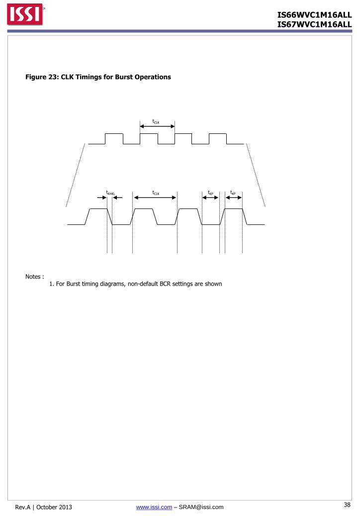
tKP tKP tCLK tKHKL
tCLK
Figure 23: CLK Timings for Burst Operations
Notes : 1. For Burst timing diagrams, non-default BCR settings are shown

IS66WVC1M16ALL IS67WVC1M16ALL
39 Rev.A | October 2013 www.issi.com – [email protected]
Figure 24: Single Access Burst READ Operation – Variable Latency without refresh collision
tCLK
Address
DQ0- DQ15
ADV#
CE#
UB#/LB#
WAIT
WE#
OE#
CLK
HiZ
VALID ADDRESS
tCEW
tSP
VALID OUTPUT
tHD
tSP tHD tKOH tACLK
tCEM
tCSP tHD
tSP tHD
tBOE
tKHTL
tHZ
Read Burst Identified (WE#=HIGH)
tABA
Notes:
1. Non-default variable latency BCR settings for single-access burst READ operation: Latency
code two (three clocks); WAIT active LOW; WAIT asserted during delay.
tOLZ

IS66WVC1M16ALL IS67WVC1M16ALL
40 Rev.A | October 2013 www.issi.com – [email protected]
Figure 25: Four-Word Burst READ Operation – Variable Latency without refresh collision
Notes:
1. Non-default variable latency BCR settings for 4-word burst READ operation: Latency code
two (three clocks); WAIT active LOW; WAIT asserted during delay.
Address
DQ0- DQ15
ADV#
CE#
UB#/LB#
WAIT
WE#
OE#
CLK
Read Burst Identified (WE#=HIGH)
tCLK
VALID ADDRESS
tSP tHD
tSP tHD tKOH tACLK
tCEM
tCSP
tHD
tSP tHD
tBOE
tOLZ
tKHTL
VALID OUTPUT
VALID OUTPUT
VALID OUTPUT
VALID OUTPUT
tCBPH
tHZ
tABA
tHZ
HiZ
tCEW
tOHZ
tSP tHD

IS66WVC1M16ALL IS67WVC1M16ALL
41 Rev.A | October 2013 www.issi.com – [email protected]
Figure 26: Four-Word Burst READ Operation – Variable Latency with refresh collision
Address
DQ0- DQ15
ADV#
CE#
UB#/LB#
WE#
CLK
Read Burst Identified (WE#=HIGH)
tCLK
VALID ADDRESS
tSP tHD
tSP tHD tKOH tACLK
tCEM
tCSP
tHD
tSP tHD
tBOE
tOLZ
tKHTL
VALID OUTPUT
VALID OUTPUT
VALID OUTPUT
VALID OUTPUT
tCBPH
tHZ
WAIT
OE#
tCEW
HiZ
tSP tHD tHZ
Notes:
1. Non-default variable latency BCR settings for 4-word burst READ operation: Latency code
two (three clocks); WAIT active LOW; WAIT asserted during delay.
2. If refresh collision happened, WAIT will be asserted between the latency count number of clock cycles
and 2x the latency count

IS66WVC1M16ALL IS67WVC1M16ALL
42 Rev.A | October 2013 www.issi.com – [email protected]
Figure 27: Single Access Burst READ Operation – Fixed Latency
tCLK
Address
DQ0- DQ15
ADV#
CE#
UB#/LB#
WAIT
WE#
OE#
CLK
VALID ADDRESS
tCEW
tSP tHD
tSP tAVH tKOH
tCEM
tCSP
tHD
tHD
tBOE
tOLZ
tKHTL
Read Burst Identified (WE#=HIGH)
VALID OUTPUT
tAA
tHZ
HiZ
tCO
tAADV
tHZ
tSP
tOHZ
Notes:
1. Non-default fixed latency BCR settings for single-access burst READ operation: Fixed Latency;
Latency code four (five clocks); WAIT active LOW; WAIT asserted during delay.
tSP tHD

IS66WVC1M16ALL IS67WVC1M16ALL
43 Rev.A | October 2013 www.issi.com – [email protected]
Figure 28: Four-Word Burst READ Operation – Fixed Latency
tCLK
Address
DQ0- DQ15
ADV#
CE#
UB#/LB#
WAIT
WE#
OE#
CLK
VALID ADDRESS
tCEW
tSP tAVH tKOH
tCEM
tCSP
tHD
tSP tHD
tBOE
tOLZ
tKHTL
Read Burst Identified (WE#=HIGH)
VALID OUTPUT
VALID OUTPUT
VALID OUTPUT
VALID OUTPUT
tCBPH
tHZ
tAA
tHZ
HiZ
tAADV
tCO
tSP tHD
tSP tHD
Notes:
1. Non-default fixed latency BCR settings for 4-word burst READ operation: Fixed latency;
latency code two (three clocks); WAIT active LOW; WAIT asserted during delay.

IS66WVC1M16ALL IS67WVC1M16ALL
44 Rev.A | October 2013 www.issi.com – [email protected]
Figure 29: READ Burst Suspend
Address
DQ0- DQ15
ADV#
CE#
UB#/LB#
WAIT
WE#
OE#
CLK
VALID ADDRESS
tCEW
tSP tHD tKOH
tCEM
tCSP
tHD
tSP tHD
tBOE
tOLZ
tKHTL
VALID OUTPUT
VALID OUTPUT
VALID OUTPUT
VALID OUTPUT
HiZ
tAADV
tCO
tSP tHD
tSP tHD
Notes:
1. Non-default BCR settings for READ burst suspend: Fixed or variable latency; latency code
two (three clocks); WAIT active LOW; WAIT asserted during delay.
2. CLK can be stopped LOW or HIGH, but must be static, with no LOW-to-HIGH transitions
during burst suspend.
3. OE# can stay LOW during BURST SUSPEND. If OE# is LOW, DQ[15:0] will continue to
output valid data.
tHD
tHD
VALID OUTPUT
VALID OUTPUT
tCBPH
tHZ
tHZ
Note2
Note3

IS66WVC1M16ALL IS67WVC1M16ALL
45 Rev.A | October 2013 www.issi.com – [email protected]
Figure 30: Burst READ at End of Row (Wrap Off)
Address
DQ0- DQ15
ADV#
CE#
UB#/LB#
WAIT
WE#
OE#
CLK
tCLK
VALID OUTPUT
VALID OUTPUT
VALID OUTPUT
VIL
VIL
VIL
tKHTL
VIH
NOTE2
VIH
tHZ
tHZ
End of Row (A[7:0]=FFh)
Notes:
1. Non-default BCR settings for burst WRITE at end of row: fixed or variable latency; WAIT
active LOW; WAIT asserted during delay.
2. For burst READs, CE# must go HIGH before the second CLK after the WAIT period begins
(before the second CLK after WAIT asserts with BCR[8] = 0, or before the third CLK after
WAIT asserts with BCR[8] = 1).

IS66WVC1M16ALL IS67WVC1M16ALL
46 Rev.A | October 2013 www.issi.com – [email protected]
Figure 31: CE#-Controlled Asynchronous WRITE
Address
DQ0- DQ15
ADV#
CE#
UB#/LB#
WAIT
OE#
WE#
HiZ HiZ
VALID ADDRESS
VALID INPUT
tCW tHZ
tBW
tAW
tCEW
tWC
tHZ
tWR
tAS
tWPH tWP
tDW tDH
tLZ
tWHZ

IS66WVC1M16ALL IS67WVC1M16ALL
47 Rev.A | October 2013 www.issi.com – [email protected]
Figure 32: LB#/UB#-Controlled Asynchronous WRITE
Address
DQ0- DQ15
ADV#
CE#
UB#/LB#
WAIT
OE#
WE#
HiZ HiZ
VALID ADDRESS
VALID INPUT
tCW tHZ
tBW
tAW
tCEW
tWC
tHZ
tWR
tAS
tWPH tWP
tDW tDH
tLZ
tWHZ

IS66WVC1M16ALL IS67WVC1M16ALL
48 Rev.A | October 2013 www.issi.com – [email protected]
Figure 33: WE#-Controlled Asynchronous WRITE
Address
DQ0- DQ15
ADV#
CE#
UB#/LB#
WAIT
OE#
WE#
HiZ HiZ
VALID ADDRESS
VALID INPUT
tCW tHZ
tBW
tAW
tCEW
tWC
tHZ
tWR
tAS
tWPH tWP
tDW tDH
tLZ
tWHZ
tAS

IS66WVC1M16ALL IS67WVC1M16ALL
49 Rev.A | October 2013 www.issi.com – [email protected]
Figure 34: Asynchronous WRITE Using ADV#
Address
DQ0- DQ15
ADV#
CE#
UB#/LB#
WE#
tVP
tAVS tAVH
VALID ADDRESS
VALID DATA
tCW
tVS
tWP
tBW
tCVS
tDW tDH
tAS
tAS
tAW
WAIT HiZ HiZ
tCEW
tHZ

IS66WVC1M16ALL IS67WVC1M16ALL
50 Rev.A | October 2013 www.issi.com – [email protected]
Figure 35: Four-Word Burst WRITE Operation – Variable Latency
Write Burst Identified (WE#=LOW)
Notes:
1. Non-default BCR settings for burst WRITE operation, with fixed-length burst of 4, burst wrap enabled:
Variable latency; latency code two (three clocks); WAIT active LOW; WAIT asserted during delay.
2. WAIT asserts for LC cycles for both fixed and variable latency. LC = latency code (BCR[13:11]).
3. tAS required if tCSP > 20ns.
Address
DQ0- DQ15
ADV#
CE#
UB#/LB#
WAIT
WE#
CLK
NOTE3
tCLK
VALID ADDRESS
tCEW
tSP tHD tHD
tCEM
tCSP
tHD
tSP tHD
tKHTL
DATA IN DATA IN DATA IN DATA IN
tCBPH
HiZ
tSP
tHD
tSP
tAS
tAS
tHD
NOTE2
IS66WVC1M16ALL IS67WVC1M16ALL
51 Rev.A | October 2013 www.issi.com – [email protected]
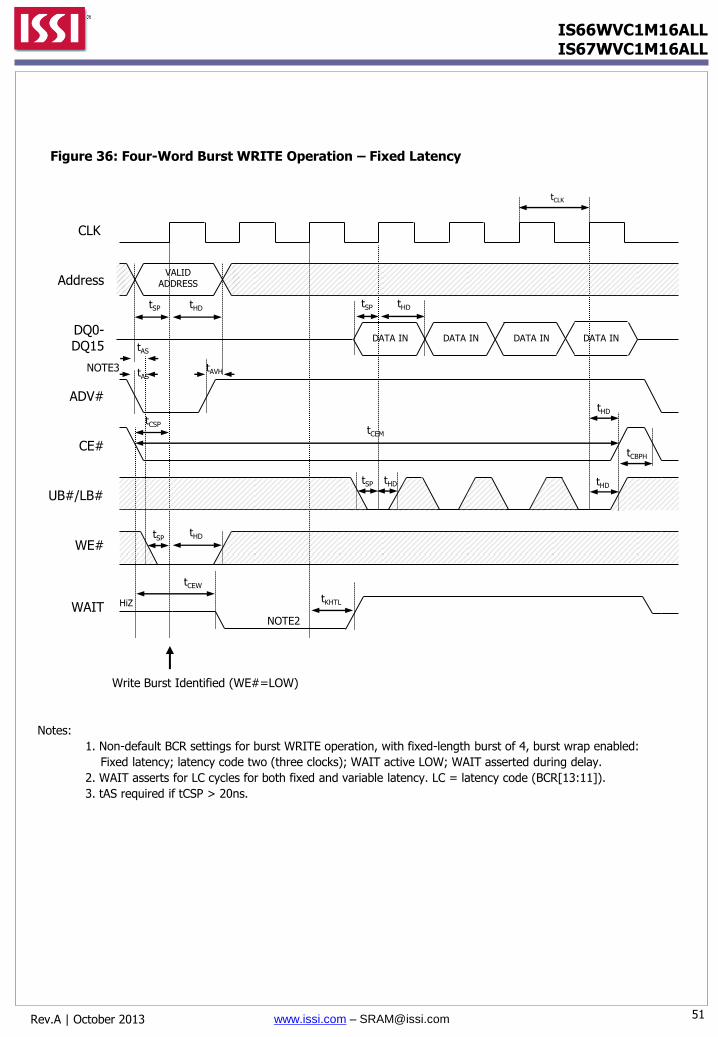
Figure 36: Four-Word Burst WRITE Operation – Fixed Latency
tCLK
Address
DQ0- DQ15
ADV#
CE#
UB#/LB#
WAIT
WE#
CLK
VALID ADDRESS
tCEW
tAVH
tSP tHD tHD
tCEM
tCSP
tHD
tSP tHD
tKHTL
Write Burst Identified (WE#=LOW)
DATA IN DATA IN DATA IN DATA IN
tCBPH
HiZ
tSP
tHD
tSP
tAS
tAS NOTE3
Notes:
1. Non-default BCR settings for burst WRITE operation, with fixed-length burst of 4, burst wrap enabled:
Fixed latency; latency code two (three clocks); WAIT active LOW; WAIT asserted during delay.
2. WAIT asserts for LC cycles for both fixed and variable latency. LC = latency code (BCR[13:11]).
3. tAS required if tCSP > 20ns.
tHD
NOTE2

IS66WVC1M16ALL IS67WVC1M16ALL
52 Rev.A | October 2013 www.issi.com – [email protected]
Figure 37: Burst WRITE at End-of-Row (Wrap Off)
Address
ADV#
UB#/LB#
WE#
OE#
CLK
tCLK
VIH
VIH
Notes:
1. Non-default BCR settings for burst WRITE at end of row: fixed or variable latency; WAIT
active LOW; WAIT asserted during delay.
2. For burst WRITEs, CE# must go HIGH before the second CLK after the WAIT period begins
(before the second CLK after WAIT asserts with BCR[8] = 0, or before the third CLK after
WAIT asserts with BCR[8] = 1).
WAIT
tKHTL tHZ
DQ0- DQ15
CE#
VALID INPUT
VALID INPUT
VALID INPUT
VIL
VIH
tHZ
End of Row (A[7:0]=FFh)
NOTE2
tHZ

IS66WVC1M16ALL IS67WVC1M16ALL
53 Rev.A | October 2013 www.issi.com – [email protected]
VALID ADDRESS
tSP tHD tKOH tACLK
tCEM
tHD
tBOE
tOLZ
tKHTL
VALID OUTPUT
VALID OUTPUT
VALID OUTPUT
VALID OUTPUT
tABA
tHZ
HiZ tCEW
tOHZ
Figure 38: Burst WRITE followed by Burst READ
Address
DQ0- DQ15
ADV#
CE#
UB#/LB#
WAIT
WE#
OE#
CLK
Notes:
1. Non-default BCR settings for burst WRITE followed by burst READ; latency code two (three clocks);
WAIT active LOW; WAIT asserted during delay.
2. A refresh opportunity must be provided every tCEM. A refresh opportunity is satisfied by either of the
following two conditions: a) clocked CE# HIGH, or b) CE# HIGH for longer than 15ns. CE# can stay
LOW between burst READ and burst WRITE operations, but CE# must not remain LOW longer than
tCEM. See burst interrupt diagram (Figure 39 through 44) for cases where
CE# stay LOW between bursts.
tCLK
VALID ADDRESS
tCEW
tSP tHD tHD
tCEM
tCSP
tSP
tKHTL
DATA IN DATA IN DATA IN DATA IN
tCBPH
HiZ
tSP
tHD
tSP
tAS
tAS
tHD

IS66WVC1M16ALL IS67WVC1M16ALL
54 Rev.A | October 2013 www.issi.com – [email protected]
Figure 39: Burst READ interrupted by Burst READ
Address
DQ0- DQ15
ADV#
CE#
UB#/LB#
WAIT
WE#
OE#
CLK
Notes:
1. Non-default BCR settings for burst READ interrupted by burst READ : fixed or variable latency;
latency code 2 (3 clocks); WAIT active LOW; WAIT asserted during delay. All bursts shown
for variable latency; no refresh collision.
2. Burst interrupt shown on first allowable clock (such as after the first data received by the controller).
3. CE# can stay LOW between burst operations, but CE# must not remain LOW longer than tCEM
VALID ADDRESS
VALID ADDRESS
tCEW
tSP tHD
tCSP
VALID OUTPUT
HiZ
tACLK
tSP tHD
tKOH tKOH tACLK
tBOE
tOLZ
VALID OUTPUT
VALID OUTPUT
VALID OUTPUT
VALID OUTPUT
tHZ
tKHTL
tOHZ
tOHZ
tBOE
tSP tHD
tCEM (Note3)
WRITE burst interrupted with new READ

IS66WVC1M16ALL IS67WVC1M16ALL
55 Rev.A | October 2013 www.issi.com – [email protected]
Figure 40: Burst READ interrupted by Burst WRITE
Address
DQ0- DQ15
ADV#
CE#
UB#/LB#
WAIT
WE#
OE#
CLK
Notes:
1. Non-default BCR settings for burst READ interrupted by burst WRITE: fixed or variable latency;
latency code 2 (3 clocks); WAIT active LOW; WAIT asserted during delay. All bursts shown
for variable latency; no refresh collision.
2. Burst interrupt shown on first allowable clock (such as after the first data received by the controller).
3. CE# can stay LOW between burst operations, but CE# must not remain LOW longer than tCEM
VALID ADDRESS
VALID ADDRESS
tCEW
tSP tHD
tCSP
VALID OUTPUT
HiZ
tACLK
tSP tHD
tKOH
VALID INPUT
VALID INPUT
VALID INPUT
VALID INPUT
tKHTL
tOHZ
tBOE
tHD tCEM (Note3)
WRITE burst interrupted with new WRITE

IS66WVC1M16ALL IS67WVC1M16ALL
56 Rev.A | October 2013 www.issi.com – [email protected]
Figure 41: Burst WRITE interrupted by Burst READ – Variable Latency Mode
Address
DQ0- DQ15
ADV#
CE#
UB#/LB#
WAIT
WE#
OE#
CLK
Notes:
1. Non-default BCR settings for burst WRITE interrupted by burst READ in variable latency mode:
fixed or variable latency; latency code 2 (3 clocks); WAIT active LOW; WAIT asserted during delay.
All bursts shown for variable latency; no refresh collision.
2. Burst interrupt shown on first allowable clock (such as after first data word written).
3. CE# can stay LOW between burst operations, but CE# must not remain LOW longer than tCEM.
VALID ADDRESS
VALID ADDRESS
tCEW
tSP tHD
tCSP
VALID INPUT
HiZ
tSP tHD
tKOH tACLK
tBOE
tOLZ
VALID OUTPUT
VALID OUTPUT
VALID OUTPUT
VALID OUTPUT
tHZ
tKHTL
tOHZ
tCEM (Note 3)
WRITE burst interrupted with new READ
tSP tHD

IS66WVC1M16ALL IS67WVC1M16ALL
57 Rev.A | October 2013 www.issi.com – [email protected]
Figure 42: Burst WRITE interrupted by Burst WRITE – Variable Latency Mode
Address
DQ0- DQ15
ADV#
CE#
UB#/LB#
WAIT
WE#
OE#
CLK
Notes:
1. Non-default BCR settings for burst WRITE interrupted by WRITE: fixed or variable latency;
latency code 2 (3 clocks); WAIT active LOW; WAIT asserted during delay. All bursts shown
for variable latency; no refresh collision.
2. Burst interrupt shown on first allowable clock (such as after the first data received by the controller).
VALID ADDRESS
VALID INPUT
VALID INPUT
VALID INPUT
VALID INPUT
tKHTL
tHD
VALID ADDRESS
tCEW
tSP tHD
tCSP
VALID INPUT
tSP tHD
WRITE burst interrupted with new WRITE
tCEM (Note 3)
tSP tHD

IS66WVC1M16ALL IS67WVC1M16ALL
58 Rev.A | October 2013 www.issi.com – [email protected]
Figure 43: Burst WRITE interrupted by Burst READ – Fixed Latency Mode
Address
DQ0- DQ15
ADV#
CE#
UB#/LB#
WAIT
WE#
OE#
CLK
Notes:
1. Non-default BCR settings for burst WRITE interrupted by burst READ in fixed latency mode:
fixed latency; latency code 2 (3 clocks); WAIT active LOW; WAIT asserted during delay.
2. Burst interrupt shown on first allowable clock (such as after first data word written).
3. CE# can stay LOW between burst operations, but CE# must not remain LOW longer than tCEM.
VALID ADDRESS
VALID ADDRESS
tCEW
tSP tAVH
tCSP
VALID INPUT
HiZ
tSP tHD
tKOH tACLK
tBOE
tOLZ
VALID OUTPUT
VALID OUTPUT
VALID OUTPUT
VALID OUTPUT
tHZ
tKHTL
tOHZ
tCEM (Note 3)
WRITE burst interrupted with new READ
tSP tHD

IS66WVC1M16ALL IS67WVC1M16ALL
59 Rev.A | October 2013 www.issi.com – [email protected]
Figure 44: Burst WRITE interrupted by Burst WRITE – Fixed Latency Mode
Address
DQ0- DQ15
ADV#
CE#
UB#/LB#
WAIT
WE#
OE#
CLK
Notes:
1. Non-default BCR settings for burst WRITE interrupted by burst WRITE in fixed latency mode:
fixed latency; latency code 2 (3 clocks); WAIT active LOW; WAIT asserted during delay.
2. Burst interrupt shown on first allowable clock (such as after first data word written).
3. CE# can stay LOW between burst operations, but CE# must not remain LOW longer than tCEM.
VALID ADDRESS
VALID INPUT
VALID INPUT
VALID INPUT
VALID INPUT
tKHTL
tHD
VALID ADDRESS
tCEW
tSP
tCSP
VALID INPUT
tSP tHD
tAVH
tHD tSP
tCEM (Note 3)

IS66WVC1M16ALL IS67WVC1M16ALL
60 Rev.A | October 2013 www.issi.com – [email protected]
Figure 45: Asynchronous WRITE followed by Burst READ
Address
DQ0- DQ15
ADV#
CE#
UB#/LB#
WAIT
WE#
OE#
CLK
tCLK
VALID ADDRESS
tSP
VALID OUTPUT
tHD
tSP tHD tKOH tACLK
tCSP tHD
tSP tHD
tBOE
tOLZ
tKHTL
tHZ
tCBPH
NOTE2
HiZ
tVP
VALID ADDRESS
VALID DATA
tCW
tVS
tWP
tBW
tCVS
tDS tDH
tAW
Notes:
1. Non-default BCR settings for asynchronous WRITE followed by burst READ: fixed or variable
latency; latency code 2 (3 clocks); WAIT active LOW; WAIT asserted during delay.
2. When transitioning between asynchronous and variable-latency burst operations, CE# must
go HIGH. CE# can stay LOW when transitioning to fixed-latency burst READs. A refresh
opportunity must be provided every tCEM. A refresh opportunity is satisfied by either of the
following two conditions: a) clocked CE# HIGH or b) CE# HIGH for longer than 15ns.
tWR

IS66WVC1M16ALL IS67WVC1M16ALL
61 Rev.A | October 2013 www.issi.com – [email protected]
Figure 46: Asynchronous WRITE (ADV# LOW) followed by Burst READ
Address
DQ0- DQ15
ADV#
CE#
UB#/LB#
WAIT
WE#
OE#
CLK
tCLK
VALID ADDRESS
tSP
VALID OUTPUT
tHD
tSP tHD tKOH tACLK
tCSP tHD
tSP tHD
tBOE
tOLZ
tKHTL
tHZ
tCBPH
NOTE2
Notes:
1. Non-default BCR settings for asynchronous WRITE followed by burst READ: fixed or variable
latency; latency code 2 (3 clocks); WAIT active LOW; WAIT asserted during delay.
2. When transitioning between asynchronous and variable-latency burst operations, CE# must
go HIGH. CE# can stay LOW when transitioning to fixed-latency burst READs. A refresh
opportunity must be provided every tCEM. A refresh opportunity is satisfied by either of the
following two conditions: a) clocked CE# HIGH or b) CE# HIGH for longer than 15ns.
VALID ADDRESS
VALID DATA
tCW
tWP
tBW
tDW tDH
tWC
tWPH
HiZ HiZ
tCEW
tHZ
tAW tWR
tLZ tWHZ tAS

IS66WVC1M16ALL IS67WVC1M16ALL
62 Rev.A | October 2013 www.issi.com – [email protected]
Figure 47: Burst READ Followed by Asynchronous WRITE (WE#-Controlled)
Notes:
1. Non-default BCR settings for burst READ followed by asynchronous WE#-controlled WRITE:
fixed or variable latency; latency code 2 (3 clocks); WAIT active LOW; WAIT asserted during delay.
2. When transitioning between asynchronous and variable-latency burst operations, CE# must
go HIGH. CE# can stay LOW when transitioning from fixed-latency burst READs. A refresh
opportunity must be provided every tCEM. A refresh opportunity is satisfied by either of the
following two conditions: a) clocked CE# HIGH or b) CE# HIGH for longer than 15ns.
tCLK
Address
DQ0- DQ15
ADV#
CE#
UB#/LB#
WAIT
WE#
OE#
CLK
HiZ
VALID ADDRESS
tCEW
tSP
VALID OUTPUT
tHD
tSP tHD tKOH tACLK
tCEM
tCSP tHD
tSP tHD
tBOE
tOLZ
tKHTL
tHZ
tABA
VALID ADDRESS
VALID DATA
tCW
tWP
tBW
tDW tDH tAS
tWC
HiZ
tCEW
tHZ
tAW tWR
tLZ
tWHZ

IS66WVC1M16ALL IS67WVC1M16ALL
63 Rev.A | October 2013 www.issi.com – [email protected]
Figure 48: Burst READ Followed by Asynchronous WRITE Using ADV#
Notes:
1. Non-default BCR settings for burst READ followed by asynchronous WRITE using ADV#: fixed
or variable latency; latency code 2 (3 clocks); WAIT active LOW; WAIT asserted during delay.
2. When transitioning between asynchronous and variable-latency burst operations, CE# must
go HIGH. CE# can stay LOW when transitioning from fixed-latency burst READs. A refresh
opportunity must be provided every tCEM. A refresh opportunity is satisfied by either of the
following two conditions: a) clocked CE# HIGH or b) CE# HIGH for longer than 15ns.
tCLK
Address
DQ0- DQ15
ADV#
CE#
UB#/LB#
WAIT
WE#
OE#
CLK
HiZ
VALID ADDRESS
tCEW
tSP
VALID OUTPUT
tHD
tSP tHD tKOH tACLK
tCEM
tCSP tHD
tSP tHD
tBOE
tOLZ
tKHTL
tHZ
tABA
VALID ADDRESS
VALID DATA
tCW
tWP
tBW
tDW tDH tAS
tWC
HiZ HiZ
tCEW
tHZ
tAW tWR
tLZ
tWHZ
tCVS

IS66WVC1M16ALL IS67WVC1M16ALL
64 Rev.A | October 2013 www.issi.com – [email protected]
Figure 49: Asynchronous WRITE followed by Asynchronous READ – ADV# LOW
Notes:
1. When configured for synchronous mode (BCR[15] = 0), CE# must remain HIGH for at least
5ns (tCPH) to schedule the appropriate refresh interval. Otherwise, tCPH is only required
after CE#-controlled WRITEs.
Address
DQ0- DQ15
ADV#
CE#
UB#/LB#
WAIT
WE#
VALID ADDRESS
VALID DATA
tCW
tWP
tBW
tDW tDH
tWC
tWPH
HiZ HiZ
tCEW
tHZ
tAW tWR
tLZ tWHZ tAS
HiZ
VALID ADDRESS
VALID OUTPUT
tCO
tOE
tHZ
tOLZ
tBA
tBLZ
tRC
tBHZ
tOHZ
tCEW
tHZ
tAA
Note1
tCPH
OE#

IS66WVC1M16ALL IS67WVC1M16ALL
65 Rev.A | October 2013 www.issi.com – [email protected]
Figure 50: Asynchronous WRITE followed by Asynchronous READ
Notes:
1. When configured for synchronous mode (BCR[15] = 0), CE# must remain HIGH for at least
5ns (tCPH) to schedule the appropriate refresh interval. Otherwise, tCPH is only required
after CE#-controlled WRITEs.
Address
DQ0- DQ15
ADV#
CE#
UB#/LB#
WAIT
WE#
HiZ HiZ HiZ
VALID ADDRESS
VALID OUTPUT
tCO
tOE
tHZ
tOLZ
tBA
tBLZ
tRC
tBHZ
tOHZ
tCEW
tHZ
tAA
VALID ADDRESS
VALID DATA
tCW
tWP
tBW
tDW tDH tAS
tWC
tWPH
tCEW
tHZ
tAW tWR
tLZ
tWHZ
tCVS
OE#

IS66WVC1M16ALL IS67WVC1M16ALL
66 Rev.A | October 2013 www.issi.com – [email protected]
Ordering Information – VDD = 1.8V
Industrial Temperature Range: (-40oC to +85oC)
Config. Speed (ns)
Frequency (MHz)
Orderable Part No. Package
1Mx16 70 133 IS66WVC1M16ALL-7013BLI 54-ball VFBGA
104 IS66WVC1M16ALL-7010BLI 54-ball VFBGA
80 IS66WVC1M16ALL-7008BLI 54-ball VFBGA
Automotive(A1) Temperature Range: (-40oC to +85oC)
Config. Speed (ns)
Frequency (MHz)
Orderable Part No. Package
1Mx16 70 104 IS67WVC1M16ALL-7010BLA1 54-ball VFBGA
