13 international conference on development and · pdf filewireless networks, ... computer...
TRANSCRIPT
13th International Conference on DEVELOPMENT AND APPLICATION SYSTEMS, Suceava, Romania, May 19-21, 2016
978-1-5090-1993-9/16/$31.00 ©2016 IEEE
A Novel PUF-Based Encryption Protocol for Embedded System On Chip
Alexandra Stanciu, Florin Dumitru Moldoveanu Department of Automatics and Information Technology
Transilvania University of Brasov Brasov, Romania
Marcian Cirstea Department of Computing and Technology
Anglia Ruskin University Anglia
Abstract—This paper presents a novel security mechanism for sensitive data stored, acquired or processed by a complex electronic circuit implemented as System-on-Chip (SoC) on an FPGA reconfigurable device. Such circuits are increasingly used in embedded or cyber systems employed in civil and military applications. Managing security in the overarching SoC presents a challenge as part of the process of securing such systems. The proposed new method is based on encrypted and authenticated communications between the microprocessor cores, FPGA fabric and peripherals inside the SoC. The encryption resides in a key generated with Physically Unclonable Function (PUF) circuits and a pseudorandom generator. The conceptual design of the security circuit was validated through hardware implementation, testing and analysis of results.
Keywords—physically unclonable functions, pseudorandm generators, security, system-on-chip, embedded system
I. INTRODUCTION
The modern Field Programmable Gate Array (FPGA) combines the programmability of processors with the performance of custom hardware. Due to their advantages, FPGAs have become the primary computational element in many critical embedded systems. Face recognition systems, wireless networks, intrusion detection systems and supercomputers, all of which are employed in large security applications, also use FPGAs [1]. As most other circuits, systems implemented on FPGAs require secure operations and communications. Design outsourcing has become increasingly common over the past 15 years for Integrated Circuits (ICs) generally and in particular for SoCs. In particular, a tendency to outsource the design and verification of the Intellectual Property (IP) core circuits and the manufacturing of integrated circuits can be noticed. Because of the globalization of the semiconductor design and fabrication processes, ICs are becoming increasingly vulnerable to malicious activities and alterations. Even if the participants are reliable, attacks like reverse engineering the bitstream, side channels attacks, manipulating the design through JTAG, initiating single
We hereby aknowledge the structural founds project PRO-DD (POS-CCE, O.2.2.1., ID 123, SMIS 2637, ctr. No. 11/2009) for providing the infrastructure used in this work.
events upset to cause functional changes to the design and other security attacks against embedded systems could appear. An example of a general model of multibit Differential Power Analysis (DPA) attacks to precharged buses, with emphasis on symmetric-key cryptography algorithms, is discussed in [2].
Modern computer systems are built on a foundation of software components from a variety of vendors. While critical applications may undergo extensive testing and evaluation procedures, the heterogeneity of software sources threatens the integrity of the execution environment for these trusted programs [3]. A similar case applies to SoCs: modern SoCs are built on a foundation of IP cores from a variety of vendors. Integration of untrusted third-party IPs into a SoC design is a major challenge in establishing trustworthiness of the entire SoC.
The proposed method is based on hardware isolation of peripherals that process critical data from peripherals that process ordinary data and on an encrypted data transfer inside the SoC, between microprocessor(s) and peripherals. The isolation and encryption are implemented at the hardware layer.
A range of countermeasures against embedded systems security attacks were developed and analyzed. Those mentioned further refer only to information encryption or application isolation at hardware level. A microprocessor designed for executing computer programs which are stored encrypted in memories to prevent software piracy is presented in [4]. Another architecture with execute-only code, which is stored in an encrypted form and may be decrypted by the instruction-loading path on the main processor chip, is introduced in [5]. In [6] the focus is on physical non-invasive attacks – or board level attacks – conducted on buses between the SoC and off-chip volatile memory or directly in the memory. The method presented ensures the confidentiality of the off-chip memory content during storage or execution in order to prevent the leakage of any sensitive information. It also ensures its integrity to forbid execution of intentionally altered data. The authors of [7] present a summary of the homomorphic encryption that consists of computations carried
158

out on ciphertext, thus generating an encrypted result which, when decrypted, matches the result of operations performed on unencrypted data. However, these computations involve complex resources and high computing time, thus making them inappropriate for embedded systems or SoC. The concept presented in this paper takes security a step forward and encrypts the transferred data between peripherals inside a SoC.
Separation and isolation are fundamental to the design of cryptographic devices. They may be found in many forms, from hardware to application at the architecture level. The authors of [8] present an approach which achieves information flow isolation between trusted and untrusted IP cores. Their method - , Gate-level information-flow tracking (GLIFT) - uses additional logic to monitor the security level of every bit in the system as they flow through Boolean gates. GLIFT associates a single-bit security label to each data-bit and tracks this information as it flows through the system [8]. Another mechanism based on isolation, physical isolation this time, is presented in [9]. They proposed a spatial isolation mechanism called a moat and a controlled sharing mechanism called a drawbridge. A moat surrounds a core with a channel in which routing is disabled; drawbridges allow signals to cross moats, letting the cores communicate with the outside world. The aim of this physical isolation is to counteract some attacks against SoC security.
The concept presented in this paper uses logical isolation between microprocessors and peripherals according to the sensitivity of transferred information. The security protocol introduced is based on data encryption/decryption with a symmetric cryptographic algorithm, trying to maintain the performance and the latency of the system. The symmetric algorithm is a pseudorandom generator (PRG) one, starting with a unique device value generated with physically unclonable functions (PUF) circuits and computing pseudo random cryptographic keys with Salsa20/20. An overview of the most important implementation details and experimental results for the PUFs is presented in [21], whereas the Salsa20/20 is introduced in [22].
II. SOC THREAT MODEL
Generally, cryptography applications or security mechanisms involve computations based on one or more secret keys. The security of a cryptosystem is only as strong as the secrecy of the key. Thus, some of the most effective attacks on a cryptosystem are based on finding flaws in the protocol that manages the keys. Attacks that may be thwarted by the introduced method are shown bellow.
One threat model for SoC is represented by physical attacks. Physical attacks against ICs assume the physical investigation of IC in order to obtain some sensitive information. Physical investigation of an IC refers to researching the parts of the IC that are not available through normal input/output pins. For example, attackers may inspect the IC layout in order to obtain the secret key. Those types of
attacks are hard to achieve due to high equipment costs. Even so, there are companies specialized in reverse engineering that analyze the circuits and structure of semiconductors and electronic systems that may lead to disclosure of secrets -one of them is Chipworks.
Bus monitoring attacks are another type of security threat against SoC. The bus between the SoC and memory is one of the most vulnerable points in the system: an adversary may easily listen on bus in order to extract information from the system. Bus monitoring attacks could also reveal access patterns to memories which may reveal sensitive information. For example, AES implementations use table of precomputed values. The order in which the table entries are accessed can reveal secret information [10]. Andrew “bunnie” Huang shows in [11] an attack against Xbox video game console from Microsoft, demonstrating that the bus is one of the weakest points in an embedded system. Although the code is stored encrypted in memory, the instructions are transferred in clear on the bus. Thus, code can be easily intercepted and the high speed of the bus is not a security protocol against bus snooping attacks.
In modern embedded systems, cores communicate with each other via shared bus. Unfortunately, the shared nature of traditional bus architecture raises several security issues. Malicious cores can obtain secrets by snooping on the bus. In addition, the bus can be used as a covert channel to leak secret data from one core to another. One of the IP cores (for example, the Ethernet controller) may contain a malicious hardware modification, a Trojan hardware that could leak information and secret keys that are being transferred between peripherals via bus. A hardware Trojan is a malicious modification of hardware during design or fabrication which causes an IC to have altered functional behavior with security consequences. A possible example of hardware Trojan insertion is presented in [12]. Israeli jets bombed a suspected nuclear installation in northeastern Syria. It was not long before military and technology bloggers concluded that this was an incident of electronic warfare. Post after post speculated that commercial off-the-shelf microprocessors in the Syrian radar might have been purposely fabricated with a hidden “backdoor”. By sending a preprogrammed code to those chips, an unknown antagonist had disrupted the chips’ function and temporarily blocked the radar.
III. SOC THREAT MODEL
The security concept of this paper consists of an analysis between computer networks and SoCs. Due to their complexity and possible attacks, SoCs may be viewed as a computer network: the SoC microprocessors represent the computer network servers, and the SoC peripherals represent the computer network clients. In terms of security threats, SoC is also similar with some computer networks attacks: spoofing attacks, when a malicious IP core can impersonate another one, covert channel to leak secret data from one core to another, or memory attacks for reading or overwriting the
159

critical data. The newly introduced method aims to experimentally validate and analyze the use of cryptographic- based operations (encryption/decryption, authentication) inside SoCs with minimum costs in terms of hardware resources or performance. The mechanism consists of the following methodology:
A. Dividing SoC peripherals into domains
The security protocol is based on logical isolation of sensitive IP cores and non-sensitive IP cores. Sensitive IP cores refer to IP cores that process sensitive information like passwords, information involved in cryptographic operations that may lead to disclosure of critical data. It is required to divide the SoC peripherals in critical and non-critical domains. The critical domain contains information flow which processes sensitive data. The processor and peripherals from the non-critical domain process trivial information. In this way, information level isolation is carried out. The division of IP cores into critical IP cores and non-critical IP cores is performed by a trust person such as the architecture system.
B. Generating PUF secret keys
The secret key is generated using PUF circuits. A PUF is a circuit that measures the inherent and random manufacturing variations presented in a device in order to generate a unique signature/cryptographic key in response to an input (challenge). PUF circuits are implemented as hard macros, this meaning that every instance is built identically: the gates are placed on the same locations and the propagation times between the gates are identical for any two instances. Theoretically, the responses of the PUF circuits have the same value, even if the instances are placed on different FPGAs/ICs or on the same FPGA/IC but in different locations. Practically, there will be differences between the responses of PUF circuits due to process variations. To instantiate multiple PUF circuits, a cryptographic key unique to each FPGA/IC due to uniqueness of process variations may be created. The FPGA or IC may be divided in a convenient number of sub-circuits, and for each sub-circuit a PUF secret key may be generated. One sub-circuit with one PUF secret key is associated with one domain from Section A. An integrated circuit may be seen as several smaller integrated circuits.
C. Encryption and Decryption
This step involves the addition of a wrapper beside peripherals and microprocessors containing the necessary mechanism to encrypt and decrypt sensitive data inside the critical domain. The wrapper contains a cryptographic key, pseudorandom generator, and the control logic in order to encrypt or decrypt the data transmitted or received. The microprocessor from the critical domain must also have the possibility to encrypt or decrypt the data stored in memories.
The transfer between peripherals inside the SoCs or embedded systems is quickly made during a few clock cycles (generally one clock cycle). In order to maintain the performance of the system, the encryption/decryption
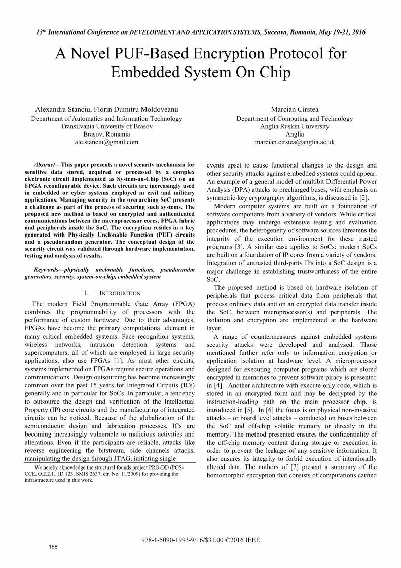
operations should not alter the transfer time between the IP cores. In order to define an efficient protocol, (running in one/two clock cycles), a stream cipher was used, where the plaintext digits are combined with a pseudorandom cipher digit stream (keystream). The key is a pseudo random bit string as long as the message. The message is XORed with the key, which assumes a very fast encryption and decryption algorithm. The security mechanism must offer the possibility to generate the same key both at the transmitter and the receiver: each peripheral has a wrapper that contains the key generation mechanism. Furthermore, the mechanisms inside one domain are synchronized. With this mechanism, the messages transferred on shared bus are encrypted. When one encrypted message is transferred on the system bus, all the peripherals inside the domain have the possibility to generate the decrypted key using PUF circuits. Fig. 1 shows the general encrypted mechanism between the microprocessor and one peripheral inside a domain.
D. Data transfer between domains
It is possible to have information that must be exchanged between different critical domains. In this case, it is necessary to generate a common key between two domains.
Periferic Wrapper
Microprocesor Peripheral
PRG_Salsa_based PRG_Salsa_based
xor xorPlaintext
data
Plaintextdata
Crypto_data
Crypto_key
Crypto_key
Address Signals
Control Signals
Microprocessor Wrapper
PUF 128bNonce 64b
Fig. 1. Encryption Scheme between Microprocessor and Peripherals.
Another key with the same length as the transferred messages may be generated using PUF circuits, in both domains. The PUF circuits may be chosen from the ones used to generate the input data for PRG. Considering that the keys are generated using the PUF circuits and according to experimental results, obtained by [17, 21] regarding the Hamming inter-distance, it may be considered that the difference in bits between the two keys is around 50%. Thus, an error correcting code to correct the n/2-1 bits from the total length of n bits may be applied for each key. The scheme of generating a common cryptographic key from two binary sequences with 49% different bits is described below. The BCH error correcting code consisting of two steps has been used:
a) The helper data phase. This phase, illustrated in Fig. 2a, is used only once per domain. It takes the cryptographic key generated by PUF circuits and generates helper data. The helper data will be available in the non-critical domain in order to reconstruct the common secret key. This stage
160
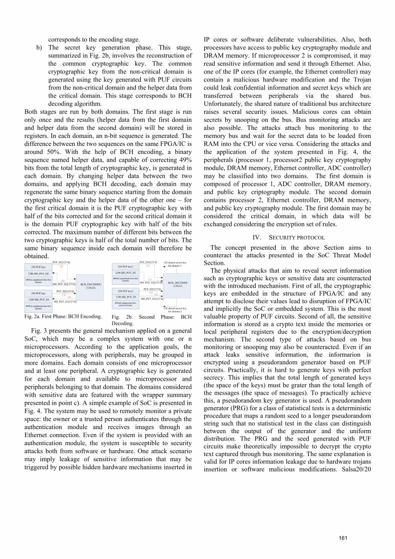
corresponds to the encoding stage. b) The secret key generation phase. This stage,
summarized in Fig. 2b, involves the reconstruction of the common cryptographic key. The common cryptographic key from the non-critical domain is generated using the key generated with PUF circuits from the non-critical domain and the helper data from the critical domain. This stage corresponds to BCH decoding algorithm.
Both stages are run by both domains. The first stage is run only once and the results (helper data from the first domain and helper data from the second domain) will be stored in registers. In each domain, an n-bit sequence is generated. The difference between the two sequences on the same FPGA/IC is around 50%. With the help of BCH encoding, a binary sequence named helper data, and capable of correcting 49% bits from the total length of cryptographic key, is generated in each domain. By changing helper data between the two domains, and applying BCH decoding, each domain may regenerate the same binary sequence starting from the domain cryptographic key and the helper data of the other one – for the first critical domain it is the PUF cryptographic key with half of the bits corrected and for the second critical domain it is the domain PUF cryptographic key with half of the bits corrected. The maximum number of different bits between the two cryptographic keys is half of the total number of bits. The same binary sequence inside each domain will therefore be obtained.
256 PUF key
MPSoC peripherals from first Domain
256 PUF key
MPSoC peripherals from first Domain
PUF_D1[127:0]
HD_PUF_D2[127:0]
128b HD_PUF_D2
128b HD_PUF_D1
PUF_D2[127:0]
HD_PUF_D1[127:0]
(1)
(2)
(3)
(4)
BCH_ENCODING(128,63)
Fig. 2a. First Phase: BCH Encoding.
256 PUF key1
MPSoC peripherals from first Domain
256 PUF key2
MPSoC peripherals from second Domain
PUF_D1[127:0]
HD_PUF_D2[127:0]
128b HD_PUF_D2
128b HD_PUF_D1
PUF_D2[127:0]
HD_PUF_D1[127:0]
(2)
(1)
(1)
(2)
BCH_DECODER(128,63)
128 shared secret key for domain 1
128 shared secret key for domain 2
Fig. 2b. Second Phase: BCH Decoding.
Fig. 3 presents the general mechanism applied on a general SoC, which may be a complex system with one or n microprocessors. According to the application goals, the microprocessors, along with peripherals, may be grouped in more domains. Each domain consists of one microprocessor and at least one peripheral. A cryptographic key is generated for each domain and available to microprocessor and peripherals belonging to that domain. The domains considered with sensitive data are featured with the wrapper summary presented in point c). A simple example of SoC is presented in Fig. 4. The system may be used to remotely monitor a private space: the owner or a trusted person authenticates through the authentication module and receives images through an Ethernet connection. Even if the system is provided with an authentication module, the system is susceptible to security attacks both from software or hardware. One attack scenario may imply leakage of sensitive information that may be triggered by possible hidden hardware mechanisms inserted in
IP cores or software deliberate vulnerabilities. Also, both processors have access to public key cryptography module and DRAM memory. If microprocessor 2 is compromised, it may read sensitive information and send it through Ethernet. Also, one of the IP cores (for example, the Ethernet controller) may contain a malicious hardware modification and the Trojan could leak confidential information and secret keys which are transferred between peripherals via the shared bus. Unfortunately, the shared nature of traditional bus architecture raises several security issues. Malicious cores can obtain secrets by snooping on the bus. Bus monitoring attacks are also possible. The attacks attach bus monitoring to the memory bus and wait for the secret data to be loaded from RAM into the CPU or vice versa. Considering the attacks and the application of the system presented in Fig. 4, the peripherals (processor 1, processor2 public key cryptography module, DRAM memory, Ethernet controller, ADC controller) may be classified into two domains. The first domain is composed of processor 1, ADC controller, DRAM memory, and public key criptography module. The second domain contains processor 2, Ethernet controller, DRAM memory, and public key cryptography module. The first domain may be considered the critical domain, in which data will be exchanged considering the encryption set of rules.
IV. SECURITY PROTOCOL
The concept presented in the above Section aims to counteract the attacks presented in the SoC Threat Model Section.
The physical attacks that aim to reveal secret information such as cryptographic keys or sensitive data are counteracted with the introduced mechanism. First of all, the cryptographic keys are embedded in the structure of FPGA/IC and any attempt to disclose their values lead to disruption of FPGA/IC and implicitly the SoC or embedded system. This is the most valuable property of PUF circuits. Second of all, the sensitive information is stored as a crypto text inside the memories or local peripheral registers due to the encryption/decryption mechanism. The second type of attacks based on bus monitoring or snooping may also be counteracted. Even if an attack leaks sensitive information, the informarion is encrypted using a pseudorandom generator based on PUF circuits. Practically, it is hard to generate keys with perfect secrecy. This implies that the total length of generated keys (the space of the keys) must be grater than the total length of the messages (the space of messages). To practically achieve this, a pseudorandom key generator is used. A pseudorandom generator (PRG) for a class of statistical tests is a deterministic procedure that maps a random seed to a longer pseudorandom string such that no statistical test in the class can distinguish between the output of the generator and the uniform distribution. The PRG and the seed generated with PUF circuits make theoretically impossible to decrypt the crypto text captured through bus monitoring. The same explanation is valid for IP cores information leakage due to hardware trojans insertion or software malicious modifications. Salsa20/20
161

starting with values generated with PUF circuits was used as a pseudorandom generator. The problem with using the Salsa PRG for encryption and decryption in System on Chip is that
the length of the stream cipher is 702 bytes = 732 bits and the
length of the messages is 32 bits = 52 . It is possible to
encrypt 5
73
2
2 = 682 messages. This is a large number of
messages but still small for a system on chip running continuously for decades or more. In order to increase the size of the output space of the original PRG, it is possible to build new PRGs out of old PRGs. For a fixed key and a nonce there
are 682 pseudorandom keys of 32 bits length generated with Salsa20/20 PRG. It is possible to use those pseudorandom keys as a nonce input or key input into another Salsa20/20 PRG. However, the sequence of the PRG is different between devices and between domains due to differences in PRG inputs: the PUF cryptographic keys.
Bus System
Up1_1Ip1_1 Ip1_n
Up2_1Ip2_1 Ip2_n
Up1_1Ip1_1 Ip1_n
Up2_1Ip2_1 Ip2_n
PUF_1 PUF_2
PUF_3PUF_4
Upm_1Ipm_1 Ipm_n
PUF_m
Encryption/Decryption
Authentication
Key Generation
Encryption/Decryption
Authentication
Key Generation
Fig. 3. General System on Chip.
Processor1
Processor2
ADC
DRAM Public Key Cryptography
Ethernet
User input
Data from external world
HDMI
User output
Fig. 4. System on Chip.
V. RESULTS AND DISCUSSION
The results are correlated with the methodology presented in Section III. All the implementations were done on Spartan 3E FPGA, XC3S500E and Virtex 4, XC4VFX20.
A. Dividing SoC peripherals into domains
The Spartan 3E is a small FPGA family with limited hardware resources. However, the FPGA may be divided in small areas, one for each SoC domain. In each area, the PUF
circuits and the IP cores may be manually placed and routed using Xilinx Planahead or Xilinx FPGA Editor. Placing and routing may be controlled using Xilinx Synthesis Constraints. In case of complex designs, larger FPGAs may be considered.
B. Generating PUF secret keys
This subject was widely discussed in [15 16, 17, 18] and a brief description is presented below. Despite many PUF circuits presented in scientific literature, few of them are suitable for FPGA implementations due to routing complexity and limitations. After analyzing most Silicon circuits, two of them were found to be appropriate for FPGA implementations: the Ring Oscillator PUF and the Latch Based PUF. Instantiating more PUF circuits from the same type, a cryptographic key is generated based on process variations and embedded in physical FPGA structure. The main properties of PUF circuits (randomness and uniqueness) were analyzed in [15, 16, 17] which considered 30 identical Spartan 3E devices. The use of the Ring Oscillator PUF and the latch based PUF to generate a unique identifier for FPGA devices are validated through the results obtained. Moreover, it has been demonstrated that distinct IDs on the same FPGA and distinct IDs for each domain or IP cores may exist on the same device. This will allow the implementation of the presented security protocol where IP cores are divided into different security level domains, and each domain has a different PUF ID.
C. Encryption and Decryption
The security protocol assumes to adjoin a wrapper that has access to the sequence generated with PUF for one domain and contains a pseudorandom generator. The chosen pseudorandom generator is Salsa20/20. Mathematical details and implementation are presented in [19]. Salsa20 generates the stream in 64-byte (512) blocks. It maps a 256-bit key, a 64-bit nonce, and a 64-bit stream position to a 512 bit output. The key is generated using 128 PUF circuits and the value is concatenated two times in order to obtain 256-bit key. Each block is an independent hash of the key, the nonce, and a 64-bit block number; there is no chaining from one block to the next.
The Salsa20 encryption function is a long chain of three simple operations on 32-bit words: 32-bit additions, 32-bit exclusive-or and constant-distance 32 bit rotation. Salsa20/20 starts with an initial state, first applies the operations for columns and then for rows. It repeats this 20 times and the final phase adds the initial state to the final result. The Salsa20 algorithm computes the pseudorandom value; 512 bits are generated in 21 clock cycles. The messages transferred on the system are presented in Fig. 1 and are 32 bits in length. In order to experimentally analyze the security concept, each peripheral was featured with this wrapper. The implementation of Salsa20/20 core was made on a Spartan 3E board and the summary of device utilization may be seen in Fig. 5. The frequency after synthesis is 139.451 MHz.
162

Fig. 5 Hardware resources for Salsa20/20.
The proposed theoretical security concept was validated using a SoC implemented on Spartan 3E FPGA, XC3S500E and Virtex 4, XC4VFX20, using IP cores from the rich library available in the Xilinx IP Catalog. The security mechanism introduced in this paper may be used inside SoCs implemented with both IP cores imported from different libraries or in-house developed custom IP cores. The experimental implementation has two approaches. The first approach uses the simulation model of Xilinx IP Cores and attaches a wrapper besides peripherals and microprocessor and it corresponds to the case when access to the input/output interface and to the logic implementation is allowed. The first approach may be applied when IP core designers implement the security mechanism. The second approach uses a coprocessor together with processor in order to encrypt/decrypt the data. The second approach corresponds to the case where access to the input/output interfaces or to the logic implementation is not allowed. In the second approach, the system architecture (which uses the IP Cores from third parties) integrates both the peripherals and the security mechanism. Both approaches were implemented in Xilinx EDK and simulated using Isim Simulator in order to validate the results. The values obtained from PUF generators are missing in the simulation. Their values may be used only in the hardware implementations.
1) The First approach In order to show that the security concept may be
implemented in a real application, a simple SoC was created with Xilinx IP Cores: Microblaze microprocessor, a custom cryptographic (crypto) peripheral with two read/write registers and a GPIO configured for LEDs. The communication inside SoC between peripherals is made through Xilinx PLB bus. The system is presented in Fig. 6. The microprocessor runs a simple C program that reads the value from register 0 of the crypto peripheral, increments the value, and writes back to the register and to the GPIO for LEDs. The communication between microprocessor and crypto peripheral must be encrypted involving that both the microprocessor and crypto peripheral need the encryption/decryption mechanism. In order to adjoin the wrapper it is necessary to understand the PLB bus protocol and the Microblaze architecture. The signals used for data transfer in case of PLB bus, Microblaze microprocessor and crypto peripheral are presented in Fig. 7, Fig. 8 and Fig. 9. Because of its instruction set architecture, Microblaze is similar to the RISC-based architecture described in [13]. In general, most Microblaze instructions are executed in one clock cycle, maintaining single-cycle throughput [14]. In order to encrypt and decrypt the data sent or received by
Microblaze two instructions are important: LW and SW. LW rA, rB, RD loads a word from the word aligned memory location that results from adding the contents of register rA and rB. The data is placed in register rD. SW rA, rB, rD stores the contents of register rD, into the word aligned memory location that results from adding the contents of registers rA and rB [14].
Fig. 6. System on Chip implemented on FPGA.
Fig. 7. PLB signals.
Fig. 8. Microblaze signals.
Fig. 9. Custom peripheral signals.
The sequence of signals corresponding to a write operation executed by Microblaze is described further. Crypto peripheral register 0 is loaded with the decimal value “10” through the SW assembly instruction. The pseudorandom cryptographic key is active 4 clock cycles. This timing was chosen in order to synchronize the microprocessor pseudo random generator with the peripheral pseudo random generator. The choice was made based on instruction execution latency and the number
163

of cycles necessary for a bus transfer. In the case of crypto peripheral, the pseudo generator mechanism is delayed with one clock cycle in order to synchronize the data transfer which has one clock cycle latency. For example, the data transferred between Microblaze and crypto peripheral has the value 0x0000000a and the pseudo random cryptographic key used for encryption/decryption has the value 0x1e68c1ce. Therefore the encrypted value sent on the PLB bus has the value 0x1e68c1c1.
The sequence of signals corresponding to a read operation executed by Microblaze is described further. It is a SW assembly instruction: the Microblaze copies the value from register 0 of crypto peripheral into one of its data registers. Fig. 10 indicates that the data read by Microblaze from the crypto peripheral has the value 0x00000014 and the pseudo random cryptographic key used for encryption/decryption has the value 0x391d1ea3.
2) The Second approach A coprocessor in order to encrypt/decrypt the received or transmitted data by or from microprocessor had been added. This version with IP cores from Xilinx IP Catalog may also be tested both on simulation and hardware. The coprocessor is a custom IP core that connects to the microprocessor through special buses. The software application has special functions in order to use the coprocessor. For the security protocol the coprocessor contains the PUF generated cryptographic key and the Salsa20/20 pseudorandom generator. In case of Microblaze and coprocessor, there is a special bus named FSL (Fast Simplex Link) available in the IP Catalog. The coprocessor is connected to Microblaze as can be seen in Fig. 10. In order to send data to coprocessor and to read data from processor, two software instructions are implemented: write_into_fsl(value) and read_from_fsl(value). Each of the two instructions has a latency of 5 clock cycles. After 10 clock cycles, Microblaze has the encrypted data and it can start the data transfer to another peripheral. The total cycle for transfer and encryption of the data between Microblaze and a peripheral is 19 clock cycles.
Fig. 10. Coprocessor connected to Microblaze.
The details regarding the sequence of signals for data transfer between Microblaze and a peripheral was presented in the first approach. Considering that each of the two operations of reading and writing have a latency of 19 clock cycles, the encryption and decryption are made combinational. Given that the Salsa20/20 (based on PUF circuits) generates the PRG key in 21 clock cycles, the mechanisms from Microblaze and peripheral are sychronized; one instance of Salsa20/20 was used. The hardware resources occupied by the SoC with coprocessor for crypotgraphic operations, on Virtex 4, xc4vfx20, are presented in Fig. 11.
Fig. 11 Hardware resources.
The validation of the proposed method is achieved through implementation results. The encryption\decryption mechanism does not affect the system’s performance or the system’s latency. There is a cost of hardware resources for implementation of this method, which is worth paying when it comes to application security. However, in most designs, the cost of hardware resources is preferable to the cost of performance or speed.
D. Data transfer between domains
In the case presented in this paper, the data width is 32 bits length. This means that a shared key between two domains with 32 bits width length is needed. In this case, in each domain, 32 bits may be considered from the total 128 bits generated with PUF circuits. From these 32 bits, a 32 bits length shared key may be obtained using the methodology with BCH encoding and decoding. The shared key may be used to encrypt the data using combinational operations to scramble the bits between the data and the shared key.
VI. CONCLUSION
The paper presents a theoretical concept for a complex SoC with more than one microprocessor and validates experimentally its significant benefits through a simple implementation of cryptographic operations in a SoC. The hardware implementation can easily be extended to accommodate a more complex SoC.
The method presented in this paper uses symmetric key algorithms in order to thwart some security issues against SoC. Considering other research results reported in this field, it can be stated that the encryption/decryption mechanism is for the first time introduced at the SoC level, between IP cores. The typical disadvantage of using symmetric key algorithms – obtaining the same cryptographic key for both encryption of plaintext and decryption of ciphertext - was eliminated by the use of PUF circuits and Salsa20/20 PRG. Adding the PUF circuits at the core of a PRG increases the randomness in the generator. The experimental results show
164

that the performance/speed of symmetric key algorithms may be used to construct a security mechanism at hardware level between the IP cores.
Given that a hardware implementation is much faster than a software one, the concept presented is based on hardware layers: PUF circuits are implemented on the physical layer, whereas the wrapper is added on soft or hard IP cores implemented in hardware description languages.
REFERENCES [1] T. Huffmire, B. Brotheron, T. Sherwood, R. Kastner, “Managing
Security in FPGA-Based Embedded Systems”, IEEE Design & Test of Computers, vol. 25, no. 6, pp. 509-598, Nov. 2008.
[2] M. Alioto, M. Poli, S. Rocchi, “Differential Power Analysis Attacks to Precharged Buses: A General Analysis for Symmetric-Key Cryptography Algorithms”, IEEE Trans. On Dependable and Secure Computing, vol. 7, no. 3, pp. 226-239, Aug. 2010.
[3] M.S. Kirkpatrick, H. Ghinita, E. Bertino, „Resilient Authenticated Execution of Critical Applications in Untrusted Environments“, IEEE Trans. On Dependable and Secure Computing, vol.9, no.4, pp.597-609, May 2012.
[4] R.M. Best, “Crypto Microprocessor for Executing Enciphered Programs”, U.S. Patent No. 4 278 837, July 1981.
[5] D. Lie, C. Thekkath, M. Mitchell, P. Lincoln, D. Boneh, J. Mitchell et al, “Architectural Support for Copy and Tamper Resistant Software” in Proc. Of the 9th Int’1 Conference on Architectural Support for Programming Languages and Operating Systems, Nov.2000, pp. 168-177.
[6] R. Elbaz, L. Torres, G. Sassatelli, P. Guillemin, M. Bardouillet, A. Martinez, “Block-Level Added Redundancy Explicit Authentication for Parallelized Encryption and Integrity Checking of Processor – Memory Transactions”, Trans. On Computational Science X LNCS, pp. 231-260, 2010.
[7] R.A. Popa, N. Zeldovich, “How to compute with data you can’t see – Web applications couls increase security by keeping data encrypted even during computations”, IEEE Spectrum [Online], 2015.
[8] J. Oberg, R. Kastner, “Eliminating Timming Information Flows in a Mix-Trusted System on Chip”, IEEE Design & Test, pp. 55-62, June 2013.
[9] T. Huffmire, B. Brotherton, N. Callegari, “Designing Secure Systems on Reconfigurable Hardware”, ACM Trans. On Design Automation of Electronic Systems,vol. 13, no. 3, July 2008.
[10] P. Colp, J. Zhang, J. Gleeson, S. Suneja, E. de Lara, H. Raj et al, “Protecting Data on Smartphones and Tablets from Memory Attacks”, ACM International Conference on Architectural Support for Programming Languages and Operating Systems, March 2015.
[11] Andrew “bunnie” Huang, “Keeping Secrets in Hardware: the Microsoft Xbox Case Study”, MIT, May 26, 2002
[12] S. Adee, ”The Hunt for the Kill Switch –Are chip makers building electronic trapdoors in key military hardware? The Pentagon is making its biggest effort yet to find out”, IEEE Spectrum [Online], May 2008.
[13] D.A. Patterson, J.L. Hennessy, “A survey of RISC Architecture for Desktop, Server and Embedded Computers” in Computer Organization and Design: The Hardware/Software Interface, 3rd Ed., San Francisco, 2005.
[14] Xilinx Microblaze Reference Guide, Online.
[15] A. Stanciu, M.Tudorancea, F. Moldoveanu, “A chip ID generation circuit – latch based”, in Proc. Of the Intl. Conf. on Ad. In Info. Proc. And Com. Tech – IPCT, pp. 58-64, June 2014.
[16] A. Stanciu, A. Craciun, “Generating an Unique Identifier for FPGA Devices”, in 14th International Conference on Optimization of Electrical and Electronic Equipment, pp. 802-808, Brasov, May, 2014.
[17] A. Stanciu, M. Cirstea, F.D. Moldoveanu, “A Novel FPGA Based on Latch Based Function With Security Applications”, IEEE Trans. on Industrial Electronics, Accepted.
[18] A. Stanciu, A.V. Craciun, F.D. Moldoveanu, “Pseudo-random generator using PUF circuits and Salsa stream cipher”, in Design and Technology in Electronic Packaging (SIITME), 2015 IEEE 21st International Symposium for, pp. 345-348, Brasov, Oct. 2015.
[19] H.P. Rosinger, “Connecting Customized IP to the Microblaze Soft Processor Using the Fast Simplex Link (FSL) Channel”, Xilinx Application Note, May 2004.
[20] A. Stanciu, T. Ciocoiu, F.D. Moldoveanu, “A method to handle BCH(n,k,t) algorithm over large GF(n) in practical hardware implementations”, Bulletin of the Transilvania University of Brasov, Vol.8(57), No 1-2015.
[21] A.R. Sadeghi, D. Naccache, Towards Hardware Intrinsic Security, 1st ed, ser. Information Security and Cryptography, Springer Berlin Heidelberg, Oct. 2010, ch. 1, pp. 3-37.
[22] D. J. Bernstein, „The Salsa20 family of stream cipher“, submitted to eStream, 2005.
165