128k x 8 high-speed cmos static ram march 2018 = 8.0 ma — 0.4 v vih input high voltage 2 vdd + 0.3...
TRANSCRIPT

Integrated Silicon Solution, Inc. — www.issi.com — 1-800-379-4774 1Rev. B103/23/2018
Copyright © 2018 Integrated Silicon Solution, Inc. All rights reserved. ISSI reserves the right to make changes to this specification and its products at any time without notice. ISSI assumes no liability arising out of the application or use of any information, products or services described herein. Customers are advised to obtain the latest version of this device specification before relying on any published information and before placing orders for products.
Integrated Silicon Solution, Inc. does not recommend the use of any of its products in life support applications where the failure or malfunction of the product can reasonably be ex-pected to cause failure of the life support system or to significantly affect its safety or effectiveness. Products are not authorized for use in such applications unless Integrated Silicon Solution, Inc. receives written assurance to its satisfaction, that:a.) the risk of injury or damage has been minimized;b.) the user assume all such risks; andc.) potential liability of Integrated Silicon Solution, Inc is adequately protected under the circumstances
IS63WV1288DALL/DALSIS63WV1288DBLL/DBLSIS64WV1288DBLL/DBLS
128K x 8 HIGH-SPEED CMOS STATIC RAMFEATURES
HIGH SPEED: (IS63/64WV1288DALL/DBLL)• High-speedaccesstime:8,10,12,20ns• LowActivePower:135mW(typical)• LowStandbyPower:12µW (typical)
CMOS standbyLOW POWER: (IS63/64WV1288DALS/DBLS)• High-speedaccesstime:25,35ns• LowActivePower:55mW(typical)• LowStandbyPower:12µW (typical)
CMOS standby• Singlepowersupply — Vdd1.65Vto2.2V(IS63WV1288DAxx) — Vdd 2.4V to 3.6V (IS63/64WV1288DBxx)• Multiplecenterpowerandgroundpinsfor
greater noise immunity• EasymemoryexpansionwithCE and OE options• CE power-down• Fullystaticoperation:noclockorrefresh
required• TTLcompatibleinputsandoutputs• Lead-freeavailable
DESCRIPTION
TheISSI IS63/64WV1288Dxxx is a very high-speed, low power, 131,072-word by 8-bit CMOS static RAM. TheIS63/64WV1288DBLLisfabricatedusingISSI's high-performanceCMOStechnology.Thishighlyreliableprocess coupled with innovative circuit design techniques, yields higher performance and low power consumption devices.
When CE is HIGH (deselected), the device assumes a standby mode at which the power dissipation can be re-duceddownto25µW(typical)withCMOSinputlevels.
TheIS63/64WV1288DBLLoperatesfromasingleVdd powersupply.TheIS63/64WV1288Dxxxisavailablein32-pinTSOP(TypeII),32-pinsTSOP(TypeI),48-Ball miniBGA (6mm x 8mm), 32-pin SOJ (400-mil) and 32-pin SOJ (300-mil) packages.
FUNCTIONAL BLOCK DIAGRAM
A0-A16
CE
OE
WE
128K X 8MEMORY ARRAYDECODER
COLUMN I/O
CONTROLCIRCUIT
GND
VDD
I/ODATA
CIRCUITI/O0-I/O7
MARCH 2018
2 Integrated Silicon Solution, Inc. — www.issi.com Rev. B1
03/23/2018
IS63WV1288DALL/DALSIS63WV1288DBLL/DBLSIS64WV1288DBLL/DBLS
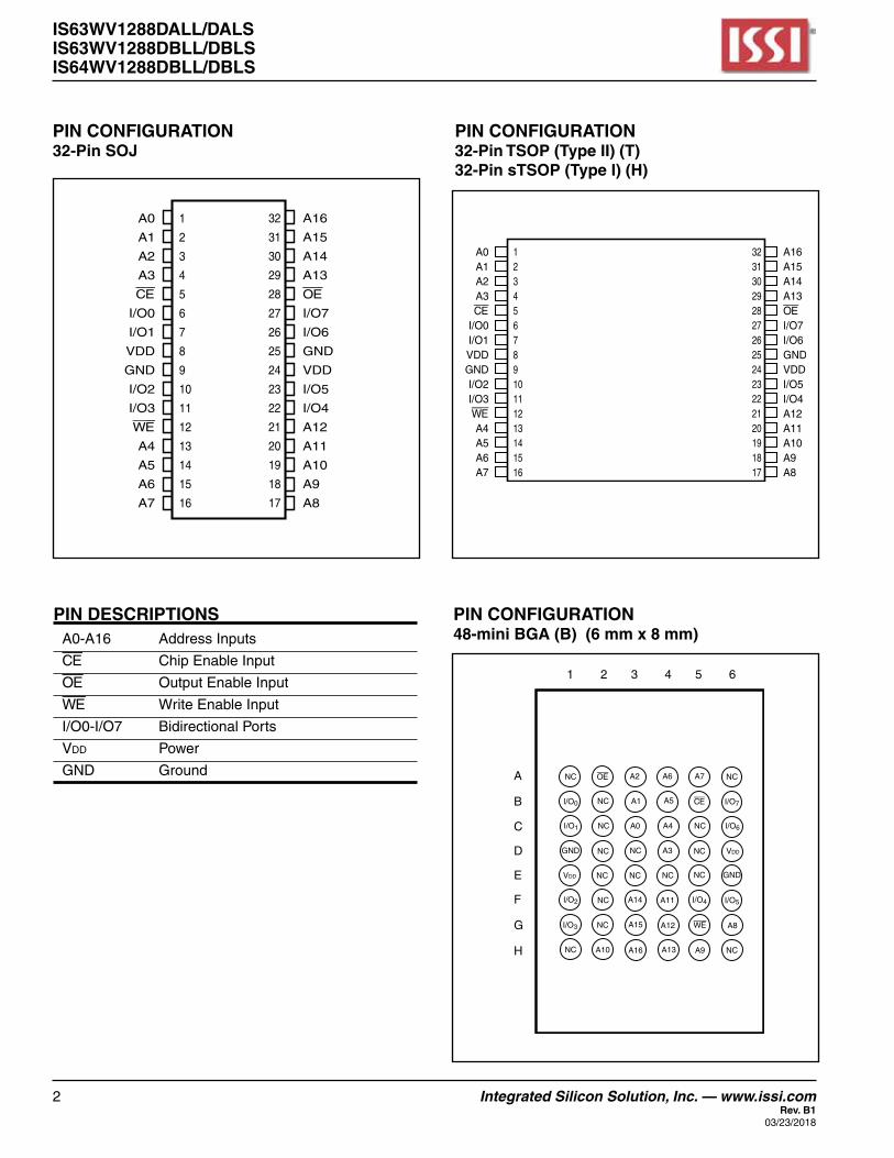
PIN DESCRIPTIONSA0-A16 Address Inputs
CE Chip Enable Input
OE Output Enable Input
WE Write Enable Input
I/O0-I/O7 Bidirectional Ports
Vdd Power
GND Ground
12345678910111213141516
32313029282726252423222120191817
A0A1A2A3CE
I/O0I/O1VDDGNDI/O2I/O3WEA4A5A6A7
A16A15A14A13OEI/O7I/O6GNDVDDI/O5I/O4A12A11A10A9A8
PIN CONFIGURATION32-Pin TSOP (Type II) (T)32-Pin sTSOP (Type I) (H)
PIN CONFIGURATION48-mini BGA (B) (6 mm x 8 mm)
PIN CONFIGURATION32-Pin SOJ
1
2
3
4
5
6
7
8
9
10
11
12
13
14
15
16
32
31
30
29
28
27
26
25
24
23
22
21
20
19
18
17
A0
A1
A2
A3
CE
I/O0
I/O1
VDD
GND
I/O2
I/O3
WE
A4
A5
A6
A7
A16
A15
A14
A13
OE
I/O7
I/O6
GND
VDD
I/O5
I/O4
A12
A11
A10
A9
A8
1 2 3 4 5 6
A
B
C
D
E
F
G
H
NC OE A2 A6 A7 NC
I/O0 NC A1 A5 CE I/O7
I/O1 NC A0 A4 NC I/O6
GND NC NC A3 NC VDD
VDD NC NC NC NC GND
I/O2 NC A14 A11 I/O4 I/O5
I/O3 NC A15 A12 WE A8
NC A10 A16 A13 A9 NC

Integrated Silicon Solution, Inc. — www.issi.com 3Rev. B103/23/2018
IS63WV1288DALL/DALSIS63WV1288DBLL/DBLSIS64WV1288DBLL/DBLS
TRUTH TABLE Mode WE CE OE I/O Operation VDD Current
Not Selected X H X High-Z Isb1, Isb2
(Power-down)
Output Disabled H L H High-Z Icc1, Icc2
Read H L L dout Icc1, Icc2
Write L L X dIn Icc1, Icc2
ABSOLUTE MAXIMUM RATINGS(1)
Symbol Parameter Value Unit Vterm TerminalVoltagewithRespecttoGND –0.5toVdd+0.5 V tstg StorageTemperature –65to+150 °C Pt PowerDissipation 1.5 W Vdd Vdd Related to GND -0.2 to +3.9 V
Note:1.StressgreaterthanthoselistedunderABSOLUTEMAXIMUMRATINGSmaycausepermanentdamagetothe
device.Thisisastressratingonlyandfunctionaloperationofthedeviceattheseoranyotherconditionsabovethose indicated in the operational sections of this specification is not implied. Exposure to absolute maximum rating conditions for extended periods may affect reliability.

4 Integrated Silicon Solution, Inc. — www.issi.com Rev. B1
03/23/2018
IS63WV1288DALL/DALSIS63WV1288DBLL/DBLSIS64WV1288DBLL/DBLS
AC TEST LOADS
Figure 1.
R1
5 pFIncluding
jig andscope
R2
OUTPUT
VTM
Figure 2.
ZO = 50Ω VDD/2
50ΩOUTPUT
30 pFIncludingjig andscope
AC TEST CONDITIONS Parameter Unit Unit Unit (2.4V-3.6V) (3.3V + 5%) (1.65V-2.2V)
Input Pulse Level 0.4V to Vdd - 0.3V 0.4V to Vdd - 0.3V 0.4V to Vdd - 0.3V
InputRiseandFallTimes 1V/ns 1V/ns 1V/ns
InputandOutputTiming VDD/2 VDD+0.05 0.9V and Reference Level (VRef) 2
OutputLoad SeeFigures1and2 SeeFigures1and2 SeeFigures1and2
R1 ( Ω ) 1909 317 13500
R2 ( Ω ) 1105 351 10800
Vtm (V) 3.0V 3.3V 1.8V

Integrated Silicon Solution, Inc. — www.issi.com 5Rev. B103/23/2018
IS63WV1288DALL/DALSIS63WV1288DBLL/DBLSIS64WV1288DBLL/DBLS
DC ELECTRICAL CHARACTERISTICS (Over Operating Range)
VDD = 2.4V-3.6V
Symbol Parameter Test Conditions Min. Max. Unit
Voh Output HIGH Voltage Vdd = Min., Ioh = –1.0mA 1.8 — V
Vol Output LOW Voltage Vdd = Min., Iol = 1.0 mA — 0.4 V
VIh Input HIGH Voltage 2.0 Vdd + 0.3 V
VIl Input LOW Voltage(1) –0.3 0.8 V
IlI Input Leakage GND ≤ VIn ≤ Vdd –1 1 µA
Ilo Output Leakage GND ≤ Vout ≤ Vdd, OutputsDisabled –1 1 µANote:1. VIl (min.) = –0.3V DC; VIl(min.)=–2.0VAC(pulsewidth<10ns).Not100%tested. VIh (max.) = Vdd + 0.3V dc; VIh (max.) = Vdd + 2.0V Ac(pulsewidth<10ns).Not100%tested.
DC ELECTRICAL CHARACTERISTICS (Over Operating Range)
VDD = 3.3V + 5%
Symbol Parameter Test Conditions Min. Max. Unit Voh Output HIGH Voltage Vdd = Min., Ioh = –4.0mA 2.4 — V Vol Output LOW Voltage Vdd = Min., Iol = 8.0 mA — 0.4 V VIh Input HIGH Voltage 2 Vdd + 0.3 V VIl Input LOW Voltage(1) –0.3 0.8 V IlI Input Leakage GND ≤ VIn ≤ Vdd –1 1 µA Ilo Output Leakage GND ≤ Vout ≤ Vdd, OutputsDisabled –1 1 µANote:1. VIl (min.) = –0.3V DC; VIl(min.)=–2.0VAC(pulsewidth<10ns).Not100%tested. VIh (max.) = Vdd + 0.3V dc; VIh (max.) = Vdd + 2.0V Ac(pulsewidth<10ns).Not100%tested.
DC ELECTRICAL CHARACTERISTICS (Over Operating Range)
VDD = 1.65V-2.2V
Symbol Parameter Test Conditions VDD Min. Max. Unit
Voh Output HIGH Voltage Ioh = -0.1mA 1.65-2.2V 1.4 — V
Vol Output LOW Voltage Iol = 0.1mA 1.65-2.2V — 0.2 V
VIh InputHIGHVoltage 1.65-2.2V 1.4 Vdd + 0.2 V
VIl(1) Input LOW Voltage 1.65-2.2V –0.2 0.4 V
IlI Input Leakage GND ≤ VIn ≤ Vdd –1 1 µA
Ilo Output Leakage GND ≤ Vout ≤ Vdd, OutputsDisabled –1 1 µANote:1. VIl (min.) = –0.3V DC; VIl(min.)=–2.0VAC(pulsewidth<10ns).Not100%tested. VIh (max.) = Vdd + 0.3V dc; VIh (max.) = Vdd + 2.0V Ac(pulsewidth<10ns).Not100%tested.

6 Integrated Silicon Solution, Inc. — www.issi.com Rev. B1
03/23/2018
IS63WV1288DALL/DALSIS63WV1288DBLL/DBLSIS64WV1288DBLL/DBLS
OPERATING RANGE (VDD) (IS63WV1288DBLL)(1)
Range Ambient Temperature VDD (8 nS)1 VDD (10 nS)1
Commercial 0°Cto+70°C 3.3V+5% 2.4V-3.6V Industrial –40°Cto+85°C 3.3V+5% 2.4V-3.6VNote:1. When operated in the range of 2.4V-3.6V, the device meets 10ns. When operated in the range of 3.3V +5%,
the device meets 8ns.
OPERATING RANGE (VDD) (IS64WV1288DBLL)(2)
Range Ambient Temperature VDD (8 nS)2 VDD (10 nS)2
Automotive –40°Cto+125°C 3.3V+5% 2.4V-3.6VNote:2. When operated in the range of 2.4V-3.6V, the device meets 10ns. When operated in the range of 3.3V +5%,
the device meets 8ns.
HIGH SPEED (IS63WV1288DALL/DBLL)OPERATING RANGE (VDD) (IS63WV1288DALL) Range Ambient Temperature VDD Speed Commercial 0°Cto+70°C 1.65V-2.2V 20ns Industrial –40°Cto+85°C 1.65V-2.2V 20ns Automotive –40°Cto+125°C 1.65V-2.2V 20ns
POWER SUPPLY CHARACTERISTICS(1) (Over Operating Range)
-8 -10 -12 -20 Symbol Parameter Test Conditions Min. Max. Min. Max. Min. Max. Min. Max. Unit
Icc Vdd Dynamic Operating Vdd = Max., Com. — 65 — 50 — 45 — 40 mA Supply Current Iout = 0 mA, f = fmAx Ind. — 70 — 55 — 50 — 45 CE = VIl Auto.(3) — — — 65 — 55 — 50 VIn ≥ Vdd – 0.3V, or typ.(2) 45 45 VIn ≤ 0.4V
Isb2 CMOS Standby Vdd = Max., Com. — 40 — 40 — 40 — 40 µA Current (CMOS Inputs) CE ≥ Vdd – 0.2V, Ind. — 55 — 55 — 55 — 55 VIn ≥ Vdd – 0.2V, or Auto. — — — 90 — 90 — 90 VIn ≤ 0.2V, f = 0 typ.(2) 4 4
Note:1. At f = fmAx, address and data inputs are cycling at the maximum frequency, f = 0 means no input lines change.2.TypicalvaluesaremeasuredatVdd=3.0V,TA=25oCandnot100%tested.3.ForAutomotivegradeat15ns,typ.Icc=38mA,not100%tested.

Integrated Silicon Solution, Inc. — www.issi.com 7Rev. B103/23/2018
IS63WV1288DALL/DALSIS63WV1288DBLL/DBLSIS64WV1288DBLL/DBLS
POWER SUPPLY CHARACTERISTICS(1) (Over Operating Range)
-25 -35 -45 Symbol Parameter Test Conditions Min. Max. Min. Max. Min. Max. Unit
Icc Vdd Dynamic Operating Vdd = Max., Com. — 15 — 15 — 12 mA Supply Current Iout = 0 mA, f = fmAx Ind. — 20 — 20 — 18 CE = VIl Auto. — 30 — 30 — 25 VIn ≥ Vdd – 0.3V, or typ.(2) 18 VIn ≤ 0.4V
Isb2 CMOS Standby Vdd = Max., Com. — 40 — 40 — 40 µA Current (CMOS Inputs) CE ≥ Vdd – 0.2V, Ind. — 50 — 50 — 50 VIn ≥ Vdd – 0.2V, or Auto. — 75 — 75 — 75 VIn ≤ 0.2V, f = 0 typ.(2) 4
Note:1. At f = fmAx, address and data inputs are cycling at the maximum frequency, f = 0 means no input lines change.2.TypicalvaluesaremeasuredatVdd=3.0V,TA=25oCandnot100%tested.
OPERATING RANGE (VDD) (IS63WV1288DBLS) Range Ambient Temperature VDD (35 nS) Commercial 0°Cto+70°C 2.4V-3.6V Industrial –40°Cto+85°C 2.4V-3.6V
LOW POWER (IS63WV1288DALS/DBLS)
OPERATING RANGE (VDD) (IS63WV1288DALS) Range Ambient Temperature VDD Speed Commercial 0°Cto+70°C 1.65V-2.2V 45ns Industrial –40°Cto+85°C 1.65V-2.2V 45ns Automotive –40°Cto+125°C 1.65V-2.2V 55ns
OPERATING RANGE (VDD) (IS64WV1288DBLS) Range Ambient Temperature VDD (35 nS) Automotive –40°Cto+125°C 2.4V-3.6V

8 Integrated Silicon Solution, Inc. — www.issi.com Rev. B1
03/23/2018
IS63WV1288DALL/DALSIS63WV1288DBLL/DBLSIS64WV1288DBLL/DBLS
READ CYCLE SWITCHING CHARACTERISTICS(1) (Over Operating Range)
-8 ns -10 ns -12 ns Symbol Parameter Min. Max. Min. Max. Min. Max. Unit
trc ReadCycleTime 8 — 10 — 12 — ns
tAA AddressAccessTime — 8 — 10 — 12 ns
tohA OutputHoldTime 2 — 2 — 2 — ns
tAce CEAccessTime — 8 — 10 — 12 ns
tdoe OEAccessTime — 4 — 5 — 6 ns
tlzoe(2) OE to Low-Z Output 0 — 0 — 0 — ns
thzoe(2) OEtoHigh-ZOutput 0 4 0 5 0 6 ns
tlzce(2) CE to Low-Z Output 3 — 3 — 3 — ns
thzce(2) CEtoHigh-ZOutput 0 4 0 5 0 6 ns
tPu CEtoPowerUpTime 0 — 0 — 0 — ns
tPd CEtoPowerDownTime — 8 — 10 — 12 ns
Notes: 1. Testconditionsassumesignaltransitiontimesof3nsorless,timingreferencelevelsof1.5V,inputpulselevelsof0to3.0Vload-
ingspecifiedinFigure1.2. TestedwiththeloadingspecifiedinFigure2.Transitionismeasured±500mVfromsteady-statevoltage.Not100%tested.
READ CYCLE SWITCHING CHARACTERISTICS(1) (Over Operating Range)
-20 ns -25 ns -35 ns -45 ns Symbol Parameter Min. Max. Min. Max. Min. Max. Min. Max. Unit
trc ReadCycleTime 20 — 25 — 35 — 45 — ns
tAA AddressAccessTime — 20 — 25 — 35 — 45 ns
tohA OutputHoldTime 2.5 — 6 — 8 — 10 — ns
tAce CEAccessTime — 20 — 25 — 35 — 45 ns
tdoe OEAccessTime — 8 — 12 — 15 — 20 ns
thzoe(2) OEtoHigh-ZOutput 0 8 0 8 0 10 0 15 ns
tlzoe(2) OE to Low-Z Output 0 — 0 — 0 — 0 — ns
thzce(2 CEtoHigh-ZOutput 0 8 0 8 0 10 0 15 ns
tlzce(2) CE to Low-Z Output 3 — 10 — 10 — 10 — nsNotes: 1. Testconditionsassumesignaltransitiontimesof1.5nsorless,timingreferencelevelsof1.25V,inputpulselevelsof0.4Vto
Vdd-0.3VandoutputloadingspecifiedinFigure1a.2. TestedwiththeloadinFigure1b.Transitionismeasured±500mVfromsteady-statevoltage.Not100%tested.3. Not100%tested.

Integrated Silicon Solution, Inc. — www.issi.com 9Rev. B103/23/2018
IS63WV1288DALL/DALSIS63WV1288DBLL/DBLSIS64WV1288DBLL/DBLS
DATA VALID
READ1.eps
PREVIOUS DATA VALID
t AA
t OHAt OHA
t RC
DOUT
ADDRESS
t RC
t OHAt AA
t DOE
t LZOE
t ACE
t LZCE
t HZOE
HIGH-ZDATA VALID
CE_RD2.eps
ADDRESS
OE
CE
DOUT
t HZCE
READ CYCLE NO. 2(1,3)
Notes: 1. WE is HIGH for a Read Cycle.2. Thedeviceiscontinuouslyselected.OE, CE = VIl.3. Address is valid prior to or coincident with CE LOW transitions.
AC WAVEFORMSREAD CYCLE NO. 1(1,2)

10 Integrated Silicon Solution, Inc. — www.issi.com Rev. B1
03/23/2018
IS63WV1288DALL/DALSIS63WV1288DBLL/DBLSIS64WV1288DBLL/DBLS
WRITE CYCLE SWITCHING CHARACTERISTICS(1,3) (Over Operating Range)
-8 ns -10 ns -12 ns Symbol Parameter Min. Max. Min. Max. Min. Max. Unit
twc WriteCycleTime 8 — 10 — 12 — ns
tsce CE to Write End 7 — 7 — 8 — ns
tAw AddressSetupTimeto 8 — 8 — 8 — ns Write End
thA Address Hold from 0 — 0 — 0 — ns Write End
tsA AddressSetupTime 0 — 0 — 0 — ns
tPwe1(1) WE Pulse Width (OE High) 7 — 7 — 8 — ns
tPwe2(2) WE Pulse Width (OE Low) 8 — 10 — 12 — ns
tsd DataSetuptoWriteEnd 5 — 5 — 6 — ns
thd Data Hold from Write End 0 — 0 — 0 — ns
thzwe(2) WELOWtoHigh-ZOutput — 4 — 5 — 6 ns
tlzwe(2) WE HIGH to Low-Z Output 3 — 3 — 3 — ns
Notes: 1. Testconditionsassumesignaltransitiontimesof3nsorless,timingreferencelevelsof1.5V,inputpulselevelsof0to3.0Vand
outputloadingspecifiedinFigure1.2. TestedwiththeloadinFigure2.Transitionismeasured±500mVfromsteady-statevoltage.Not100%tested.3. TheinternalwritetimeisdefinedbytheoverlapofCE LOW and WE LOW. All signals must be in valid states to initiate a Write,
butanyonecangoinactivetoterminatetheWrite.TheDataInputSetupandHoldtimingarereferencedtotherisingorfallingedge of the signal that terminates the Write.
WRITE CYCLE SWITCHING CHARACTERISTICS(1,2) (Over Operating Range)
-20 ns -25 ns -35 ns -45ns Symbol Parameter Min. Max. Min. Max. Min. Max. Min. Max. Unit
twc WriteCycleTime 20 — 25 — 35 — 45 — ns
tsce CEtoWriteEnd 12 — 18 — 25 — 35 — ns
tAw AddressSetupTime 12 — 15 — 25 — 35 — ns to Write End
thA Address Hold from Write End 0 — 0 — 0 — 0 — ns
tsA AddressSetupTime 0 — 0 — 0 — 0 — ns
tPwe1 WE Pulse Width (OE=HIGH) 12 — 18 — 30 — 35 — ns
tPwe2 WE Pulse Width (OE=LOW) 17 — 20 — 30 — 35 — ns
tsd DataSetuptoWriteEnd 9 — 12 — 15 — 20 — ns
thd Data Hold from Write End 0 — 0 — 0 — 0 — ns
thzwe(3) WE LOW to High-Z Output — 9 — 12 — 20 — 20 ns
tlzwe(3) WEHIGHtoLow-ZOutput 3 — 5 — 5 — 5 — ns
Notes: 1. TestconditionsforIS61WV6416LLassumesignaltransitiontimesof1.5nsorless,timingreferencelevelsof1.25V,inputpulse
levels of 0.4V to Vdd-0.3VandoutputloadingspecifiedinFigure1a.2. TestedwiththeloadinFigure1b.Transitionismeasured±500mVfromsteady-statevoltage.Not100%tested.3. TheinternalwritetimeisdefinedbytheoverlapofCE LOW and UB or LB, and WE LOW. All signals must be in valid states to
initiateaWrite,butanyonecangoinactivetoterminatetheWrite.TheDataInputSetupandHoldtimingarereferencedtotherising or falling edge of the signal that terminates the write.

Integrated Silicon Solution, Inc. — www.issi.com 11Rev. B103/23/2018
IS63WV1288DALL/DALSIS63WV1288DBLL/DBLSIS64WV1288DBLL/DBLS
AC WAVEFORMSWRITE CYCLE NO. 1(1,2 (CE Controlled, OE = HIGH or LOW)
DATA UNDEFINED
t WC
VALID ADDRESS
t SCE
t PWE1t PWE2
t AW
t HA
HIGH-Z
t HD
t SA
t HZWE
ADDRESS
CE
WE
DOUT
DIN DATAIN VALID
t LZWE
t SD
CE_WR1.eps

12 Integrated Silicon Solution, Inc. — www.issi.com Rev. B1
03/23/2018
IS63WV1288DALL/DALSIS63WV1288DBLL/DBLSIS64WV1288DBLL/DBLS
AC WAVEFORMSWRITE CYCLE NO. 2(1) (WE Controlled, OE = hIgh during Write Cycle)
WRITE CYCLE NO. 3 (WE Controlled: OE is LOW During Write Cycle)
Notes: 1. TheinternalwritetimeisdefinedbytheoverlapofCE LOW and WE LOW. All signals must be in valid states to initiate a Write,
butanyonecangoinactivetoterminatetheWrite.TheDataInputSetupandHoldtimingarereferencedtotherisingorfallingedge of the signal that terminates the Write.
2. I/O will assume the High-Z state if OE > VIh.
DATA UNDEFINED
LOW
t WC
VALID ADDRESS
t PWE1
t AW
t HA
HIGH-Z
t HD
t SA t HZWE
ADDRESS
CE
WE
DOUT
DIN
OE
DATAIN VALID
t LZWE
t SD
CE_WR2.eps
DATA UNDEFINED
t WC
VALID ADDRESS
LOW
LOW
t PWE2
t AW
t HA
HIGH-Z
t HD
tSA t HZWE
ADDRESS
CE
WE
DOUT
DIN
OE
DATAIN VALID
t LZWE
t SD
CE_WR3.eps

Integrated Silicon Solution, Inc. — www.issi.com 13Rev. B103/23/2018
IS63WV1288DALL/DALSIS63WV1288DBLL/DBLSIS64WV1288DBLL/DBLS
DATA RETENTION WAVEFORM (CE Controlled)
HIGH SPEED (IS63/4WV1288DALL/DBLL)
DATA RETENTION SWITCHING CHARACTERISTICS (2.4V-3.6V)
Symbol Parameter Test Condition Options Min. Typ.(1) Max. Unit Vdr Vdd for Data Retention See Data Retention Waveform 2.0 — 3.6 V Idr Data Retention Current Vdd = 2.0V, CE ≥ Vdd–0.2V Com. — 4 40 µA Ind. — — 55 Auto. 90 tsdr DataRetentionSetupTime SeeDataRetentionWaveform 0 — — ns trdr RecoveryTime SeeDataRetentionWaveform trc — — nsNote 1: TypicalvaluesaremeasuredatVdd=3.0V,TA = 25oc andnot100%tested.
VDD
CE ≥ VDD - 0.2V
tSDR tRDR
VDR
CEGND
Data Retention Mode
DATA RETENTION SWITCHING CHARACTERISTICS (1.65V-2.2V)
Symbol Parameter Test Condition Options Min. Typ.(1) Max. Unit Vdr Vdd for Data Retention See Data Retention Waveform 1.2 — 3.6 V Idr Data Retention Current Vdd = 1.2V, CE ≥ Vdd–0.2V Com. — 4 40 µA Ind. — — 55 Auto. — — 90 tsdr DataRetentionSetupTime SeeDataRetentionWaveform 0 — — ns trdr RecoveryTime SeeDataRetentionWaveform trc — — nsNote 1: TypicalvaluesaremeasuredatVdd=1.8V,TA = 25oc andnot100%tested.

14 Integrated Silicon Solution, Inc. — www.issi.com Rev. B1
03/23/2018
IS63WV1288DALL/DALSIS63WV1288DBLL/DBLSIS64WV1288DBLL/DBLS
DATA RETENTION WAVEFORM (CE Controlled)
LOW POWER (IS63/4WV1288DALS/DBLS)
DATA RETENTION SWITCHING CHARACTERISTICS (2.4V-3.6V)
Symbol Parameter Test Condition Options Min. Typ.(1) Max. Unit Vdr Vdd for Data Retention See Data Retention Waveform 2.0 — 3.6 V Idr Data Retention Current Vdd = 2.0V, CE ≥ Vdd–0.2V Com. — 4 40 µA Ind. — — 50 Auto. 75 tsdr DataRetentionSetupTime SeeDataRetentionWaveform 0 — — ns trdr RecoveryTime SeeDataRetentionWaveform trc — — nsNote 1: TypicalvaluesaremeasuredatVdd=3.0V,TA = 25oc andnot100%tested.
VDD
CE ≥ VDD - 0.2V
tSDR tRDR
VDR
CEGND
Data Retention Mode
DATA RETENTION SWITCHING CHARACTERISTICS (1.65V-2.2V)
Symbol Parameter Test Condition Options Min. Typ.(1) Max. Unit Vdr Vdd for Data Retention See Data Retention Waveform 1.2 — 3.6 V Idr Data Retention Current Vdd = 1.2V, CE ≥ Vdd–0.2V Com. — 4 40 µA Ind. — — 50 Auto. — — 75 tsdr DataRetentionSetupTime SeeDataRetentionWaveform 0 — — ns trdr RecoveryTime SeeDataRetentionWaveform trc — — nsNote 1: TypicalvaluesaremeasuredatVdd=1.8V,TA = 25oc andnot100%tested.

Integrated Silicon Solution, Inc. — www.issi.com 15Rev. B103/23/2018
IS63WV1288DALL/DALSIS63WV1288DBLL/DBLSIS64WV1288DBLL/DBLS
ORDERING INFORMATION
Industrial Range: –40°C to +85°C Speed (ns) Order Part No. Package
8 IS63WV1288DBLL-8TLI 32-pinTSOP(TypeII),Lead-free IS63WV1288DBLL-8HLI sTSOP(TypeI)(8mmx13.4mm),Lead-free IS63WV1288DBLL-8JLI 32-pin SOJ (300-mil), Lead-free
10 IS63WV1288DBLL-10TLI 32-pinTSOP(TypeII),Lead-free IS63WV1288DBLL-10HLI sTSOP(TypeI)(8mmx13.4mm),Lead-free IS63WV1288DBLL-10JLI 32-pin SOJ (300-mil), Lead-free IS63WV1288DBLL-10KLI 32-pin SOJ (400-mil), Lead-free
Automotive Range (A3): –40°C to +125°C Speed (ns) Order Part No. Package
10(8*) IS64WV1288DBLL-10CTLA3 32-pinTSOP(TypeII),CopperLeadframe,Lead-free IS64WV1288DBLL-10HLA3 sTSOP(TypeI)(8mmx13.4mm),Lead-freeNote:1. Speed = 8ns for Vdd=3.3V+5%.Speed=10nsforVdd = 2.4V-3.6V.

16 Integrated Silicon Solution, Inc. — www.issi.com Rev. B1
03/23/2018
IS63WV1288DALL/DALSIS63WV1288DBLL/DBLSIS64WV1288DBLL/DBLS
Integrated Silicon Solution, Inc. — www.issi.com 17Rev. B103/23/2018
IS63WV1288DALL/DALSIS63WV1288DBLL/DBLSIS64WV1288DBLL/DBLS
NO
TE :
2. D
imen
sion
D a
nd E
1 do
not
incl
ude
mol
d pr
otru
sion
.
4. F
orm
ed le
ads
shal
l be
plan
ar w
ith re
spec
t to
one
anot
her w
ithin
0.1
mm
3.
Dim
ensi
on b
2 do
es n
ot in
clud
e da
mba
r pro
trusi
on/in
trusi
on.
at t
he s
eatin
g pl
ane
afte
r fin
al te
st.
1. C
ontro
lling
dim
ensi
on :
mm
5. R
efer
ence
doc
umen
t : J
ED
EC
SP
EC
MS
-027
.
SE
ATI
NG
PLA
NE
12/1
9/20
07

18 Integrated Silicon Solution, Inc. — www.issi.com Rev. B1
03/23/2018
IS63WV1288DALL/DALSIS63WV1288DBLL/DBLSIS64WV1288DBLL/DBLS
Integrated Silicon Solution, Inc. — www.issi.com 19Rev. B103/23/2018
IS63WV1288DALL/DALSIS63WV1288DBLL/DBLSIS64WV1288DBLL/DBLS
20 Integrated Silicon Solution, Inc. — www.issi.com Rev. B1
03/23/2018
IS63WV1288DALL/DALSIS63WV1288DBLL/DBLSIS64WV1288DBLL/DBLS
2. R
efer
ence
doc
umen
t : J
ED
EC
MO
-207
1. C
ON
TRO
LLIN
G D
IME
NS
ION
: M
M .
NO
TE :
08/1
2/20
08Pa
ckag
e O
utlin
e