128 ieee transactions on biomedical …mason/pubs/ieee tbcas 2007 - dwt.pdf · area-power...
TRANSCRIPT

128 IEEE TRANSACTIONS ON BIOMEDICAL CIRCUITS AND SYSTEMS, VOL. 1, NO. 2, JUNE 2007
Area-Power Efficient VLSI Implementation ofMultichannel DWT for Data Compression in
Implantable NeuroprostheticsAwais M. Kamboh, Student Member, IEEE, Matthew Raetz, Student Member, IEEE,
Karim G. Oweiss, Member, IEEE, and Andrew Mason, Senior Member, IEEE
Abstract—Time-frequency domain signal processing of neuralrecordings, from high-density microelectrode arrays implanted inthe cortex, is highly desired to ease the bandwidth bottleneck as-sociated with data transfer to extra-cranial processing units. Be-cause of its energy compactness features, discrete wavelet trans-form (DWT) has been shown to provide efficient data compressionfor neural records without compromising the information content.This paper describes an area-power minimized hardware imple-mentation of the lifting scheme for multilevel, multichannel DWTwith quantized filter coefficients and integer computation. Perfor-mance tradeoffs and key design decisions for implantable neuro-prosthetics are presented. A 32-channel 4-level version of the cir-cuit has been custom designed in 0.18- m CMOS and occupiesonly 0.22 mm2 area and consumes 76 W of power, making ithighly suitable for implantable neural interface applications re-quiring wireless data transfer.
Index Terms—Brain–machine interface (BMI), integer liftingwavelet transform, neural signal compression, VLSI design.
I. INTRODUCTION
NEUROPROSTHETICS devices and brain–machine in-terfaces (BMIs) are increasingly playing a vital role in
helping patients with severe motor disorders achieve a betterlifestyle by enabling direct interface to the central nervoussystem at various levels. Recording the activity of corticalneurons with microelectrode arrays was shown to be essentialto quantify their degree of involvement in encoding movementparameters, thereby permitting decoding of the neural signalsto take place to control artificial limbs [1]. Such BMIs showgreat promise in many biomedical applications.
One particular challenge with BMI technology is the need totransmit the high bandwidth neural data from the implanted de-vice to the outside world for further analysis. For example, atypical recording experiment with a 100-electrode array sam-pled at 25 kHz per channel with 12-bit precision yields an ag-gregate data rate of 30 Mbps, which is well beyond the reach ofstate-of-the-art telemetry links for biological applications. An-other significant challenge is the need to fit implanted circuitry
Manuscript received March 13, 2007; revised August 20, 2007. This workwas supported in part by the National Institute of Health under Grant NS047516and in part by the National University of Sciences and Technology, Islamabad,Pakistan. This paper was recommended by Associate Editor M. Sawan.
The authors are with the Electrical and Computer Engineering Department,Michigan State University, East Lansing, MI 48824 USA (e-mail: [email protected]).
Color versions of one or more of the figures in this paper are available onlineat http://ieeexplore.ieee.org.
Digital Object Identifier 10.1109/TBCAS.2007.907557
within 1 cm for the entire signal processing system, andoperate the chip at very low power (no more than 8–10 mW)to prevent temperature rise above 1 C and avoid neural tissuedamage [2].
For implanted microelectrode arrays, the power required towirelessly transmit raw data to extra-cranial processing unitsis prohibitively large. Likewise, the hardware required to per-form full neural data analysis is too complex to be implementedwithin an implanted system. Data compression before transmis-sion is an attractive alternative, if it can be preformed with min-imal hardware resources. Discrete wavelet transform (DWT) isa very effective method for compressing neural data [3], [4]. Theresulting nonzero DWT coefficients give a sparse representationof the signal that greatly reduces the power required to uploaddata.
To utilize DWT-based compression with modern neuropros-thetics devices, a multichannel, multilevel implementation isnecessary because microelectrode arrays sample multiple datachannels simultaneously and multiple decomposition levels im-prove signal reproduction accuracy. Thus, area and power effi-cient hardware that can perform multichannel, multilevel DWTin real time is highly desirable. In contrast to traditional DWTapplications, neuroprosthetics can afford long computation in-tervals, up to 40 s [4], permitting hardware to prioritize powerand area efficiency over speed. From the hardware point of view,integer-lifting and B-spline DWT factorization schemes havevery efficient implementations. The lifting approach to the DWTreduces the required arithmetic operations and, as an in-placeimplementation, requires less memory at the expense of a longercritical path [5], [6]. The B-spline factorization reduces the crit-ical path delay by converting some of the required multiply op-erations into less computationally intensive shift-and-add oper-ations [6].
With few exceptions, recent efforts to optimize DWT hard-ware have concentrated on increasing throughput at the expenseof area and power [5], [6]. In contrast, our prior work has iden-tified an optimal implementation of the DWT architecturewhere chip area and power have priority over speed [7]. Theapproach relies on a hardware-efficient integer lifting factoriza-tion scheme and the “symmlet” family of wavelet basis that hasbeen shown to provide a near optimal compression of neuralsignals [4].
This paper describes the design of a highly area and powerefficient VLSI circuit that implements multichannel, multilevellifting-based DWT in real time. Section II explains the architec-ture used to calculate the DWT while the design decisions fora computation core (CC) are detailed in Section III. Section IV
1932-4545/$25.00 © 2007 IEEE

KAMBOH et al.: AREA-POWER EFFICIENT VLSI IMPLEMENTATION 129
Fig. 1. Data flow diagram for lifting DWT using the symmlet 4 basis.
describes optimizations in the memory modules, and Sec-tion V discusses controller operations. Results for a 32-channel4-level DWT realization are summarized and performance ofthe system is analyzed in Section VI, followed by conclusionsin Section VII.
II. ARCHITECTURE
Fig. 1 shows the data flow diagram of lifting-based DWTusing the symmlet 4 bases. If and are two sequential inputsamples from the same channel, and are approximation anddetail results, and , , and are intermediate results, the fivefilter steps in this flow can be expressed by
(1)
where are the eight constant filter coefficients and sub-scripts of the other variables represent the time sample, 0 beingthe current sample, 1 the previous sample, and so on.
To ease hardware requirements, it has been shown thatinteger lifting DWT with quantized data and filter coefficientvalues maintains a high signal to noise ratio. Based on thisanalysis, we have chosen 10-bit data and 5-bit coefficients(including sign bit) for our hardware implementation. Ourprevious work evaluated two structurally different hardwareapproaches, namely pipeline and sequential, for suitabilityin implantable devices based on their resource demands [2].Derived from this system-level analysis, we have found thatfor the single channel case, the pipeline architecture consumessmaller power at the expense of considerably larger area ascompared to the sequential architecture, resulting in a higherarea-power product. The difference in area-power productincreases with the increasing number of channels and levels,making the sequential architecture the better choice of the twoespecially for higher number of channels.
Fig. 2 describes the DWT architecture resulting from ourcircuit-level design efforts. It is composed of a customizedCC, a digital controller, and five memory modules for in-coming data, filter coefficients, intermediate CC products, andintermediate values necessary to sequentially process multiplelevels and channels. Sequential data samples (inputs and )from a given channel are processed in pairs to generate theapproximate and detail DWT coefficients (outputs and ). Toachieve system-level goals of power and area efficiency, each
Fig. 2. Complete system diagram for sequential calculation of DWT.
of these architectural blocks has been customized at the circuitlevel to minimize transistor count and eliminate unnecessaryoutput transitions.
III. COMPUTATION CORE
Analysis of the “symmlet4” lifting factorization and resultingequations in (1) show a noticeable computation regularity; allarithmetic operations can be expressed in the general form of
. This regularity can be exploited tominimize hardware by implementing a single CC that sequen-tially executes all computational steps in (1). Sequential reuse ofthe same hardware significantly reduces chip real estate require-ments without impacting performance in this low bandwidth ap-plication.
The merits of using two’s complement arithmetic versus sign-magnitude arithmetic were considered. The 10-bit input data isreceived in sign magnitude form, as are the constant 5-bit filtercoefficients. The CC multipliers are required to perform 10 5operations. Methods for multiplying sign-magnitude numbersdo not work with two’s complement numbers without adapta-tion. We have implemented several combinations of adders andmultipliers using sign-magnitude and two’s complement repre-sentation and found that it is most efficient to handle multipli-cation in sign-magnitude form while additions are performed intwo’s complement. As shown in Fig. 3, the CC can be imple-mented using two multipliers and a three-term adder formed bycascading two two-term adders. Using this CC to sequentiallyexecute the steps in (1) requires five cycles to compute resultsfor one sample pair. The critical path for this CC is ,where and are the delays of the multiplier and the adder,respectively. Overflows that can occur during these computa-tions are handled by replacing the results with appropriate pos-itive or negative saturation values.
A. Adders
Ripple carry–, carry save, and carry–look-ahead adders wereanalyzed for this DWT implementation. Because delay does notpose a bottleneck and area and power are much more important,the lower transistor count required by ripple carry adder wasfavored. Ripple carry adder performance depends largely uponstructure of its individual full-adder cells, whose properties can

130 IEEE TRANSACTIONS ON BIOMEDICAL CIRCUITS AND SYSTEMS, VOL. 1, NO. 2, JUNE 2007
Fig. 3. Computation core architecture for integer lifting DWT used to compute(1).
Fig. 4. Single bit full adder cell used in the CC adders based on pass transistorlogic [8].
vary widely to match different applications. Comparative anal-ysis of several full adder structures was performed at the cir-cuit level to take into account transistor count, activity factor,and dynamic power due to parasitics. Based on these results,the pass gate logic 1-bit full adder presented in [8] and shownin Fig. 4 was chosen to best suit our DWT application. Unlikesome adder cells with slightly lower transistor counts, this cellhas no internal direct path between power and ground, elimi-nating short circuit current during transistor switching. Further-more, the use of transmission gates limits the output voltageswing and reduces dynamic power consumption without com-promising overall speed or reliability. In 0.18- m CMOS, this16 transistor cell was designed to dissipate 0.4 W power andoccupy 41.5 m . It was utilized to construct 10-bit adders forthe three-term adder block and 13-bit adders for the 10 5 mul-tipliers.
B. Multipliers
The CC requires two multipliers to perform 10 5 oper-ations. Booth multiplication algorithm is especially suited fortwo’s complemented multiplication; however, it works well forblock multiplications. Both Booth and array multiplier struc-tures were optimized to the specific bit resolutions of our DWTapplication and compared for area and power. The Booth multi-plier consists of recoders, partial product generators, 3:2 and 2:1compressors and a final adder. The recoders and partial product
TABLE ICC TRANSISTOR COUNTS AND WORST CASE VALUES
generators were optimized for low power [9]. Two different re-coders and partial product generators were considered, both re-quiring 18 transistors each. The two partial product generatorarchitectures, NPR3a and NPR3b, presented in [9], were tai-lored to this application and it was determined that, while powerconsumption is similar, NPR3b needs slightly fewer transistors(14 versus 16) and is preferred. The 3:2 and 2:1 compressorsare full and half adders respectively. In contrast, the array mul-tiplier ANDs every bit of the multiplier with every bit of themultiplicand to create partial products. A Wallace tree structurewas implemented to compress the partial products. Both Boothand array multipliers require an adder at the final stage. In com-parison, a CC design using a Booth multiplier was shown tooccupy 16% more area than a CC design with an array multi-plier. Table I gives area, average power and delay measurementsof the custom designed adder and array multiplier sub-modulesselected for use in our DWT CC. It also includes the averagepower, area and delay measurements for the complete compu-tational core including two’s complement circuits. The averagepower includes static and dynamic power dissipation at a clockfrequency of 6.4 MHz.
IV. MEMORY MODULES
A. Multichannel/Level Memory Module
Neuroprosthetics applications generally depend upon mul-tiple data streams taken from an array of microelectrodes. Thus,our DWT system has been designed to compress data from mul-tiple channels simultaneously using multilevel decomposition inreal time. Analysis of our DWT implementation indicates thatthere is sufficient bandwidth within a single CC to process wellover 100 data channels sequentially. Sequential processing sig-nificantly reduces computational hardware demand; however,the intermediate values, or “state,” of the current channel needsto be stored in memory so they are available when the CC laterprocesses the next sample from this channel.
Similarly, memory is needed to store intermediate valueswhile switching between different levels. The memory blockrequired to hold these intermediate values is called thechannel/level memory. The values that need to be stored andmade available to process future samples are defined by (1). Foreach level and channel (beyond one), the lifting architecture re-quires five 10-bit values— , , , , and —to be saved,four of which are stored in channel/level memory while one isstored in the pairing memory. Every level and every channel re-quires a corresponding 40-bit memory register. In a 32-channel4-level design, this amounts to 128 registers. The channel/levelmemory was implemented in both an SRAM using standard sixtransistor cells and a DRAM. For a large number of channelsand levels, the channel/level memory module was found todominate the power and area of the overall DWT system.

KAMBOH et al.: AREA-POWER EFFICIENT VLSI IMPLEMENTATION 131
TABLE IICC TRANSISTOR COUNTS AND WORST CASE VALUES
For the prototype DWT chip, the channel/level memory wasimplemented in SRAM to maximize reliability and ease system-level testing. However a DRAM implementation is particularlyefficient in this application; due to the sequential nature of theDWT, the entire memory block is periodically overwritten, elim-inating the need for refresh circuitry during normal operation.For example, at a sampling rate of 25 kHz, the least frequentlyaccessed level 4 data is overwritten every 0.64 ms, which ismuch faster than the hold time easily achievable by a DRAMcell implemented in a standard CMOS process. This feature per-mits significant area savings over the SRAM implementation, asshown in Table II which compares relative performance criteriafor a 32-channel 4-level memory block.
In a standard 0.18- m CMOS process, use of a discreteDRAM storage capacitor is prohibitively area expensive. Al-ternatively, the gate capacitance of a large MOSFET has beenused to store charge. Assuming that the sense amplifiers need astored value of at least 1 V to reliably read the correct value, aMOSFET with at least 0.2- m gate area is required to realize adependable hold time. Constructed in this fashion, comparisonof two custom designed CMOS memory blocks shows that aDRAM block would permit a 64% area savings over an SRAMblock for a 32-channel 4-level implementation.
B. Input, Coefficient, Pairing, and CC Memory Modules
Because DWT operates on data pairs, there is a hold cycle be-tween each computation of input pairs wherein the first sampleof the pair is acquired. Thus, an input data buffer of size equal tothe number of channels is required to store input samples duringthe hold cycles. For the 32-channel implementation, the inputbuffer was constructed using FIFO shift registers. Note that inthis architecture, the hold cycle is used to compute all results forhigher (beyond one) levels of decomposition, where the neces-sary data is available from previous computations.
A separate coefficient memory block is required to store theeight 5-bit filter coefficients. Because this data is static, it ismost efficiently implemented using hardwired connections, ef-fectively operating as a ROM structure with only the electronicsnecessary to switch the proper coefficient values into the CC atthe appropriate computation phase.
To accommodate sequential reuse of CC hardware, at the be-ginning of each computation cycle, four intermediate resultsfrom the previous computation cycle for the same channel mustbe loaded into the CC. These values, loaded from the channel/level memory module, are stored in a block defined as the CCmemory. This CC memory block must be capable of loadingall four bytes in parallel and moving data to the appropriate CCinput as it cycles through the filter steps in (1). As describedbelow, this requires six 10-bit registers that were implementedusing flip-flops for parallel load/store and byte-wise shift oper-ations.
Fig. 5. DWT circuit operation phases for a single computation cycle.
When performing calculations for levels 2 and beyond, theCC input data ( and in Fig. 2) does not come from inputs tothe DWT circuit. Rather, inputs must be pulled from results cal-culated previously for a lower level. These values are stored ina pairing memory that must contain two 10-bit values for everychannel and level except the highest level. All computation cy-cles except those of the highest level will generate one 10-bitbyte to be written to this pairing memory. During all compu-tation cycles for level 2 and beyond, two 10-bit values will beread from this block. Due to this unique read/write structure,this block was implemented independent of the channel/levelmemory using an SRAM with address decoding circuitry thatallows us to enable each 10-bit byte block independently.
C. Power Saving Strategies for Memory
To reduce power consumption in the SRAM blocks, a dividedbit line structure [10] was adopted, reducing the overall bit linecapacitance and eliminating unnecessary dynamic power con-sumption during read and write cycles. Each of the sub bit lineswere connected to only eight SRAM cells, and extra logic withinthe decoder controls access to these sub bit lines. With reducedbit line capacitance, the SRAM could be implemented withouta sense amplifier, eliminating the need to access both sides ofthe SRAM cell and reducing bit line currents during read oper-ations.
V. CONTROLLER
The main functions of the controller are to direct overallsystem operation and route data between DWT circuit blocksat the proper time [11]. The sequence of actions needed tocomplete a single DWT computation cycle consists of threedifferent phases over a total of eight clock cycles, as shown inFig. 5. As managed by the DWT controller, one read cycle isfollowed by five calculation cycles and then two write cycles.During the read cycle, stored values from prior calculations areloaded into the CC memory. During the calculation cycles, thefive filter steps in (1) are executed. During the write cycles, re-sults are stored onto channel/level and pairing memory blocks.This sequence must be repeated for each channel within theinput sampling period. For example, with 32 data channels anda typical neural signal sampling rate of 25 kHz, the eight oper-ation cycles must be clocked at 6.4 MHz. For fewer channels,the clock rate can be reduced to ensure power is only consumedwhen computations are required.
Note that the number of levels has no effect on the clock fre-quency because higher level results will be computed duringintermediate hold cycles (see Section IV-B) while data inputpairs are being stored. This is illustrated in Fig. 6, which de-scribes the sequence of computation cycles managed by the con-troller for one channel and four levels. Here, each column repre-sents a computation cycle composed of eight clock cycles. Thenumber of computation cycles necessary for a complete, repeat-able, DWT operation sequence is , where is the number oflevels. As shown in Fig. 6, four levels requires 16 computation

132 IEEE TRANSACTIONS ON BIOMEDICAL CIRCUITS AND SYSTEMS, VOL. 1, NO. 2, JUNE 2007
Fig. 6. Per channel activity of the CC at different levels of decomposition for a 4-level implementation. The top line shows the computation cycle count, andthe next line counts the cycles within each operation sequence (two shown). A level 1 result is computed when a pair of data samples is received, a level 2 resultis computed when two level 1 results are available, and so on. The first results calculated at each level are trash values because the memory initially containsmeaningless values. After each 2 computation cycles (where L is the number of levels), there is an idle (no calc) cycle.
Fig. 7. Data movement in CC memory during the five calculation cycles withina computation cycle (one per sample per level). Top line shows the six registernames. Subsequent lines define how data must be moved as the steps in (1) areprocessed sequentially.
cycles for a complete operation sequence. Within each operationsequence ( computation cycles) one cycle will be an idle cyclewhere no computations are necessary, as indicated by NO CALCin Fig. 6. Notice that, in each odd numbered computation cycle,no level one results are being calculated. These odd cycles cor-respond to input hold cycles discussed above. While input datapairs are being stored in these cycles (to be processed in the fol-lowing cycle), the CC hardware can be utilized to process resultsfor all levels greater than one in the sequence defined by Fig. 6.Thus, an infinite number of levels could be processed withoutadditional hardware or increasing frequency. The number ofchannels has no impact on this sequence; each channel is pro-cessed sequentially within a single computation cycle, whichcan be achieved by increasing clocking frequency by a factorequal to the number of channels. Thus, the only major impactof increasing channels or levels is an increase in dynamic powerconsumption and the addition of channel/level memory.
To control the sequence and timing of operations within theDWT circuit, both an instruction based microprocessor and astate machine based controller were analyzed. Because of therelatively straightforward and repetitive nature of operations,the efficiency of a state machine design was found to be muchmore compatible with the power and area goals of this DWTcircuit. The inherent tradeoff for this efficiency is limited flexi-bility, and the maximum number of levels and channels had tobe set before implementing the state machine controller. Here
we will describe a state machine for 32 channels and 4 levels.This design assumes multichannel input data is multiplexed intoa single 10-bit input bus, and it will output results sequentiallyonto a single output bus.
For a 32-channel 4-level DWT system, the state machine con-troller utilizes a 12-bit counter to keep track of the current state,channel, and level. The three least significant bits of this counterdetermine the eight clock cycles within a computation cycle(Fig. 5) defining the operation phase for the CC and memoryblocks, regardless of the channel or level being processed. Thenext five bits of the counter specify channel being processed.The remaining four bits represent the level being processed,where each bit represents an individual level (Fig. 6). The level1 bit also determines if the input stream should go to the inputbuffer (hold cycle) or the CC (compute level 1 results). In thisfashion, a level 1 result is computed once a pair of data sam-ples is received; a level 2 result is computed when two level oneresults are available; and so on. By increasing the width of thecounter, more states could be added to support additional chan-nels or levels.
Fig. 7 describes operations within the CC memory controlledby the three least significant bits of the state machine counter.Here, complex data movement within the CC memory and itsinteraction with other memory blocks is controlled. Fig. 7 de-fines CC memory register names, where X, Y, and Z are reg-isters connected to respective inputs of the CC while M1, M2,and M3 store intermediate computation results. Values are readinto the CC memory at the beginning of the computation cycle.This is followed by five cycles of calculations and register datashifts. The last calculation cycle produces detail and approxi-mation DWT results. The detail DWT coefficient is sent to theoutput bus. The approximation DWT coefficient is sent to theoutput bus and, depending on the level being processed, storedin pairing memory. After the last calculation cycle, four of thevalues in CC memory, , , , and , are stored to thechannel/level memory for use in subsequent calculations of thecurrent channel/level results.
VI. RESULTS AND ANALYSIS
A. Final Hardware Resources
All of the DWT circuit blocks were custom designed andlaid out in 0.18- m CMOS. Table III lists number of transis-tors required for each module. The corresponding chip area re-
KAMBOH et al.: AREA-POWER EFFICIENT VLSI IMPLEMENTATION 133
TABLE IIITRANSISTOR COUNT AND AREA FOR HARDWARE MODULES
�Counts exclude transistors for address decoding circuitry
TABLE IVAVERAGE ACTIVITY PER CYCLE FOR HARDWARE MODULES
quired by each module, including routing, is also shown. Thedominance of channel/level memory over other modules is ev-ident, where increasing the number of channels by a factor offour (from 8 to 32) results in roughly a 300% increase in boththe number of transistors and the area consumption. Our model32-channel, 4-level DWT implementation, requires 54 k tran-sistors and occupies roughly 470 m 470 m. These valueswere obtained with the major memory blocks implemented withSRAM for reliability and testing purposes. If the input buffer,pairing and channel/level memory were replaced by DRAMblocks, the estimated transistor count for the 32-channel, 4-levelcircuit would drop to around 25 000 and the total DWT circuitarea would reduce to a little more than 100 000 m , which isless than 50% of the overall circuit using SRAM. Table III alsogives the area and transistor count precise estimates for 100- and250-channel designs.
A 32-channel system, with a sampling frequency of 25 KHz,operating at 4 levels of DWT decomposition requires a clockfrequency of 6.4 MHz. The power is managed separately foreach block, thus the hardware portions not working at a giventime do not consume any power. As described in Section V,operation of the DWT block can be modeled as a state machinewhich requires 8 cycles to complete its operation, as shown inFig. 5. Table IV gives the average activity per cycle of eachhardware module.
If the maximum delay of 10 ns is considered to allow for ef-fects of fabrication non idealities, it allows us time to process500 channels, at 25 KHz sampling frequency, in a time-mul-tiplexed fashion. However handling of 500 channels does notseem feasible especially at the analog-to-digital converters andthe neural signal amplifiers.
The overall 32-channel 4-level system at 0.18- m processtechnology with 1.3 V and at 6.4 MHz of operating fre-quency consumes an average power of 76 W, including static
and dynamic power dissipation, with highest power being con-sumed by CC memory, the CC and the controller respectively.Since these three modules are operational most of the time, theyaccount for about 80% of the total power.
B. Data Compression Versus MSE
The DWT circuit outputs interleaved approximate and de-tail transform coefficients that give a sparse representation ofthe original neural signal. Coefficient values below a specificthreshold can be set to zero to compress the results into a smallernumber of bytes. The nonzero coefficients can then be encodedusing a lossless encoding scheme and transmitted to the extra-cranial or extra-cutaneous processing units [4], [12]. Choosingthe value of the zeroing threshold provides a tradeoff betweensignal integrity and compression ratio.
To test our DWT circuit implementation on real neural data,a linear-step analog to digital converter was used to convert ex-perimentally obtained neural data into a stream of 10-bit digitalvalues. The data was then processed through the DWT systemand results were stored for analysis. In one test, the stored trans-form coefficients were used to reconstruct the neural signal, andthis result was compared to the original signal to measure thequality of reconstruction. This analysis was performed for sev-eral different zeroing threshold values to evaluate signal qualityverses the amount of compression obtained. The final perfor-mance metrics can be defined in terms of three quantities, theroot mean squared error (RMS), Shannon’s entropy [13], andthe assigned threshold.
RMS error is a measure of the average difference betweenthe original and the reconstructed signal. Here the differencebetween the original signal and the reconstructed signal is com-prised of two components: the quantization noise due to finite-word length, and the lossy-compression noise resulting fromthe thresholding operation. The mathematical representation ofRMS error is given by
(2)
where is the original signal, is the reconstructed signal,and is the length of the signal.
Shannon’s entropy is a measure of uncertainty associatedwith a random signal and can be interpreted as the averageminimum message length, represented in bits, which must betransmitted to communicate the exact value of the signal.
Entropy gives the theoretical limit to the best possible loss-less data compression for any communication. Entropy can bemathematically represented as
(3)
where is the total number of possible values (also called sym-bols in information theory literature) and is the probabilityof occurrence of the th value.
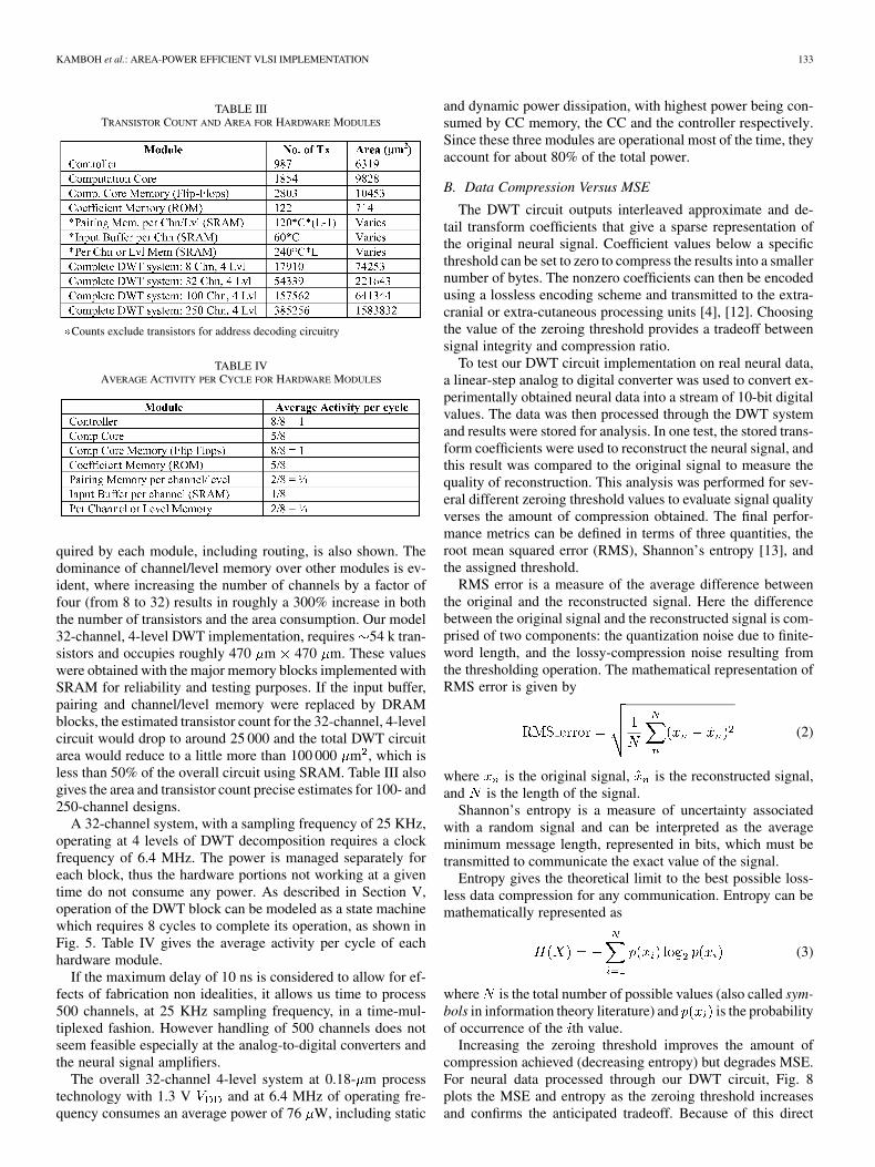
Increasing the zeroing threshold improves the amount ofcompression achieved (decreasing entropy) but degrades MSE.For neural data processed through our DWT circuit, Fig. 8plots the MSE and entropy as the zeroing threshold increasesand confirms the anticipated tradeoff. Because of this direct
134 IEEE TRANSACTIONS ON BIOMEDICAL CIRCUITS AND SYSTEMS, VOL. 1, NO. 2, JUNE 2007
Fig. 8. RMS error and entropy in bits per symbol as a function of thresholdvalue for the neural data set used in our experiments.
Fig. 9. Relation between RMS error and entropy, where the independent vari-able is the threshold.
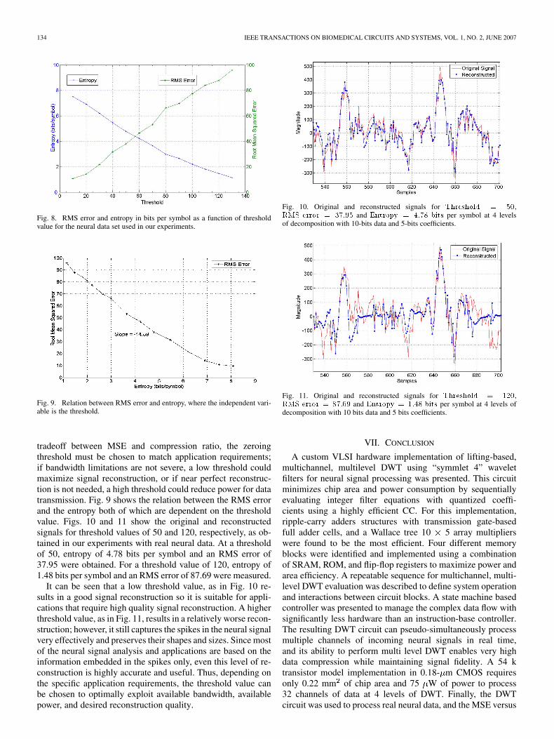
tradeoff between MSE and compression ratio, the zeroingthreshold must be chosen to match application requirements;if bandwidth limitations are not severe, a low threshold couldmaximize signal reconstruction, or if near perfect reconstruc-tion is not needed, a high threshold could reduce power for datatransmission. Fig. 9 shows the relation between the RMS errorand the entropy both of which are dependent on the thresholdvalue. Figs. 10 and 11 show the original and reconstructedsignals for threshold values of 50 and 120, respectively, as ob-tained in our experiments with real neural data. At a thresholdof 50, entropy of 4.78 bits per symbol and an RMS error of37.95 were obtained. For a threshold value of 120, entropy of1.48 bits per symbol and an RMS error of 87.69 were measured.
It can be seen that a low threshold value, as in Fig. 10 re-sults in a good signal reconstruction so it is suitable for appli-cations that require high quality signal reconstruction. A higherthreshold value, as in Fig. 11, results in a relatively worse recon-struction; however, it still captures the spikes in the neural signalvery effectively and preserves their shapes and sizes. Since mostof the neural signal analysis and applications are based on theinformation embedded in the spikes only, even this level of re-construction is highly accurate and useful. Thus, depending onthe specific application requirements, the threshold value canbe chosen to optimally exploit available bandwidth, availablepower, and desired reconstruction quality.
Fig. 10. Original and reconstructed signals for Threshold = 50,RMS error = 37:95 and Entropy = 4:78 bits per symbol at 4 levelsof decomposition with 10-bits data and 5-bits coefficients.
Fig. 11. Original and reconstructed signals for Threshold = 120,RMS error = 87:69 and Entropy = 1:48 bits per symbol at 4 levels ofdecomposition with 10 bits data and 5 bits coefficients.
VII. CONCLUSION
A custom VLSI hardware implementation of lifting-based,multichannel, multilevel DWT using “symmlet 4” waveletfilters for neural signal processing was presented. This circuitminimizes chip area and power consumption by sequentiallyevaluating integer filter equations with quantized coeffi-cients using a highly efficient CC. For this implementation,ripple-carry adders structures with transmission gate-basedfull adder cells, and a Wallace tree 10 5 array multiplierswere found to be the most efficient. Four different memoryblocks were identified and implemented using a combinationof SRAM, ROM, and flip-flop registers to maximize power andarea efficiency. A repeatable sequence for multichannel, multi-level DWT evaluation was described to define system operationand interactions between circuit blocks. A state machine basedcontroller was presented to manage the complex data flow withsignificantly less hardware than an instruction-base controller.The resulting DWT circuit can pseudo-simultaneously processmultiple channels of incoming neural signals in real time,and its ability to perform multi level DWT enables very highdata compression while maintaining signal fidelity. A 54 ktransistor model implementation in 0.18- m CMOS requiresonly 0.22 mm of chip area and 75 W of power to process32 channels of data at 4 levels of DWT. Finally, the DWTcircuit was used to process real neural data, and the MSE versus

KAMBOH et al.: AREA-POWER EFFICIENT VLSI IMPLEMENTATION 135
compression ratio tradeoff was analyzed over many values ofzeroing threshold. The small size and low power consumptionof this DWT VLSI circuit makes it highly suitable for font-enddata compression in implantable applications.
ACKNOWLEDGMENT
The authors would like to thank T. Canfield for his valuablecontributions towards this research.
REFERENCES
[1] M. Nicolelis, “Actions from thoughts,” Nature, vol. 409, 2001, pp.403–107.
[2] K. Oweiss, A. Mason, Y. Suhail, A. M. Kamboh, and K. Thomson, “Ascalable wavelet transform VLSI architecture for real-time signal pro-cessing in multichannel cortical implants,” IEEE Trans. Circuits Syst.I, Fundam. Theory Appl., vol. 54, no. 6, pp. 1266–1278, Jun. 2007.
[3] S. Mallat, A Wavelet Tour of Signal Processing. New York: Aca-demic, 1998.
[4] K. G. Oweiss, “A systems approach for data compression and latencyreduction in cortically controlled brain machine interfaces,” IEEETrans. Biomed. Eng., vol. 53, no. 7, pp. 1364–1377, Jul. 2006.
[5] H. Liao, M. K. Mandal, and B. F. Cockburn, “Efficient architecturesfor 1-D and 2-D lifting-based wavelet transforms,” IEEE Trans. SignalProcess., vol. 52, no. 5, pp. 1315–1326, May 2004.
[6] C. T. Huang, P. C. Tseng, and L. G. Chen, “VLSI architecture for for-ward discrete wavelet transform based on B-spline factorization,” J.VLSI Signal Process., pp. 343–353, 2005.
[7] A. M. Kamboh, A. Mason, and K. G. Oweiss, “Comparison of liftingand B-spline DWT implementations for implantable neuroprosthetics,”J. VLSI Signal Process. Syst., to be published.
[8] A. Shams, T. K. Darwish, and M. A. Bayoumi, “Performance analysisof low-power 1-bit CMOS full adder cells,” IEEE Trans. Very LargeScale Integr. (VLSI) Syst., vol. 10, no. 1, pp. 20–29, Feb. 2002.
[9] Z. Huang, “High-level optimization techniques for low-power multi-plier design,” Ph.D. dissertation, Comp. Sci. Dept., Univ. California,Los Angeles, 2003.
[10] B.-D. Yang and L.-S. Kim, “A low power SRAM using hierarchical bitline and local sense amplifiers,” IEEE J. Solid-State Circuits, vol. 40,no. 6, pp. 1366–1376, Jun. 2005.
[11] A. M. Kamboh, M. Raetz, A. Mason, and K. Oweiss, “Area-power ef-ficient lifting-based DWT hardware for implantable neuroprosthetics,”in Proc. IEEE Int. Symp. Circuits Syst., 2007, pp. 2371–2374.
[12] K. G. Oweiss, Y. Sohail, K. Thomson, J. Li, and A. Mason, “Aug-menting real-time DSP in implantable high-density neuroprostheticsdevices,” in Proc. IEEE/EMBS Special Topic Conf. Microtechnol. Med.Biol., 2005, pp. 108–111.
[13] C. E. Shannon, “A mathematical theory of communication,” Bell Syst.Tech. J., vol. 27, pp. 379–423, 1948.
Awais M. Kamboh (S’07) received the B.S. degree(hons.) in electrical engineering from National Uni-versity of Sciences and Technology, Islamabad, Pak-istan, in 2003, and the M.S. degree in electrical en-gineering systems from the University of Michigan,Ann Arbor, in 2006. He is currently working towardsthe Ph.D. degree at Michigan State University, EastLansing.
His research interests include signal processing,multimedia communications, VLSI and SoC design.
Mr. Kamboh is a student member of the IEEECommunications Society, IEEE Circuit and Systems Society, and the IEEEEngineering in Medicine and Biology Society.
Matthew Raetz (S’04) is currently working towardthe B.S. degree in electrical engineering fromMichigan State University, East Lansing, wherehe has been actively engaged in research with theAdvanced MicroSystem and Circuits (AMSaC)research group.
He has worked on custom mixed-signal circuits forneural signal processing and low power digital con-trol circuits for sensor-based microsystems. His re-search interests include system design and low powerintegrated circuits.
Karim G. Oweiss (S’95–M’02) received the B.S.and M.S. degrees (hons.) in electrical engineeringfrom the University of Alexandria, Alexandria,Egypt, in 1993 and 1996, respectively, and thePh.D. degree in electrical engineering and computerscience from the University of Michigan, Ann Arbor,in 2002.
He completed postdoctoral training with theBiomedical Engineering Department, University ofMichigan, Ann Arbor, in the summer of 2002. InAugust 2002, he joined the Department of Electrical
and Computer Engineering and the Neuroscience program at Michigan StateUniversity, where he is currently an Assistant Professor and Director of theNeural Systems Engineering Laboratory. His research interests span diverseareas that include statistical and multiscale signal processing, informationtheory, machine learning as well as modeling the dynamics of the nervoussystem, neural integration and coordination in sensorimotor systems, andcomputational neuroscience.
Dr. Oweiss is a member of the IEEE Society for Neuroscience. He is alsoa member of the Board of Directors of the IEEE Signal Processing Society onBrain Machine Interfaces, the Technical Committees of the IEEE BiomedicalCircuits and Systems, the IEEE Life Sciences, and the IEEE Engineering inMedicine and Biology Society. He was awarded the excellence in Neural Engi-neering award from the National Science Foundation in 2001.
Andrew Mason (S’90–M’99–SM’06) received theB.S. degree in physics (highest distinction) fromWestern Kentucky University, Bowling Green, in1991, the B.S.E.E. degree (hons.) from the GeorgiaInstitute of Technology, Atlanta, in 1992, and theM.S. and Ph.D. degrees in electrical engineeringfrom the University of Michigan, Ann Arbor, in1994 and 2000, respectively.
From 1997 to 1999, he was an Electronic SystemsEngineer at a small aerospace company, and from1999 to 2001, he was an Assistant Professor at the
University of Kentucky. In 2001, he joined the Department of Electrical andComputer Engineering, Michigan State University, East Lansing, where heis currently an Associate Professor. His research addresses many areas ofmixed-signal circuit design and the fabrication of integrated microsystems.Current projects include adaptive sensor interface circuits, bioelectrochemicalinterrogation circuits, post-CMOS fabrication of electrochemical sensors, andintegrated circuits for neural signal processing.
Dr. Mason serves on the Sensory Systems and Biomedical Circuits and Sys-tems Technical Committees of the IEEE Circuits and Systems Society and theon the Technical Program Committee for IEEE International Conference onSensors. In 2006, he received the Michigan State University Teacher-ScholarAward.