1.2 survey of dc to dc converters - home page for the...
TRANSCRIPT
the organic designer should avoid using inductors, which are present in the buck
and boost converters, because they are extremely lossy. There are other DC to DC
converters that do not use inductors, and one of the most famous is the Dickson
charge pump. The Dickson charge pump consists only of capacitors, diodes, and a
clock, which makes it an excellent candidate for organic implementation.
In a general solar cell array power system, the DC to DC converter can be designed
with an efficiency close to 100%, so it is not a limitation for powering the load. The
solar cells in the solar array and the load are the factors that affect the power efficiency
of the solar array.
This work investigates what solar cell manufacturing tolerances, loads, and power
are required to make the charge pump option more economical than the array option.
A little background on common DC to DC converters, Dickson charge pumps, and
solar cell arrays is given first. Then, simulation results are given that show what
conditions on the solar cell parameter tolerances produce situations that favor the
charge pump option.
1.2 Survey of DC to DC converters
The simplest DC to DC converter is the voltage divider using resistors. However,
there are not many voltage divider circuits in use because the non-load resistor dissi-
pates power, lowering the overall power efficiency. Optimal DC to DC converters use
switching techniques to move charge or current in such a way that creates a larger or
smaller voltage or current on the output.
1.2.1 Buck Converter
The buck converter is used to lower the input voltage. The circuit diagram is shown
in Figure 2. The waveform applied to the low-pass L-C filter, Va is a square wave and
has an average value of DVin, where D is the duty cycle of the switch. The low-pass
filter removes all the high frequency components in Va, and the output becomes just
6

Figure 2: The buck converter uses a switch and low-pass filter to lower input voltage.
the DC component [16],
Vout = Va = DVin (1)
The gain equation is linear, so a feedback loop can be used to control or regulate the
output.
1.2.2 Boost Converter
The boost converter is used to raise the input voltage. The circuit diagram is shown
in Figure 3. The inductor is first charged when the switch is closed. When the switch
opens, it discharges into the capacitor, which slowly discharges into the load. The
gain equation is [16]:
Vout =1
1 − DVin (2)
The gain equation is linear, so a feedback loop can also be used to control the output
of the boost converter.
1.2.3 Buck-Boost Converter
The buck-boost converter is used to raise or lower the input voltage. The circuit
diagram is shown in Figure 4. The buck-boost converter can be thought of as a
buck and boost converter cascaded together. The peculiarity is that the output is
inverted. The gain equation is the product of the buck and boost gain equations.
7

Figure 3: The boost converter uses a switched inductor and a ripple capacitor toraise input voltage.
Figure 4: The buck-boost converter uses a switched inductor and a blocking diodeto control how much power goes to the load.
From equations (1) and (2) [16],
Vout =D
1 − DVin (3)
The gain equation is linear, so a feedback loop can be used to control the output.
1.2.4 Cuk Converter
The Cuk converter is used to raise or lower the input voltage just like the buck-boost
converter. The circuit diagram is shown in Figure 5. This circuit was named after its
inventor, Slobodan Cuk. The gain equation is the same as the buck-boost converter
8

Figure 5: The Cuk converter uses a capacitor as its main energy storage device asopposed to an inductor like in the Buck, Boost, and Buck-Boost converters.
[16] [6]:
Vout =D
1 − DVin (4)
The gain equation is linear, so a feedback loop can be used to control the output.
1.2.5 Cockcroft-Walton Voltage Multiplier
J. D. Cockcroft and E. T. S. Walton unveiled the predecessor to the Dickson charge
pump in 1932. Their purpose was to accelerate protons to high speeds and conduct
other experiments [4]. To do that, they needed an extremely large DC voltage (800
kV exactly) to create an extremely powerful electric field, which could accelerate
protons from rest. The circuit they devised is shown in Figure 6. The basic idea
behind the circuit was charging the lower-level capacitors on the right-hand column
and then moving the switches up so that the higher left-hand capacitors could be
charged. Then, the switches would be moved again to charge even higher-level right-
hand column capacitors. This process continues until the circuit reaches steady-state,
at which time the output voltage becomes [4]
Vout = NVin (5)
where N is the number of capacitors in the left-hand column. The maximum voltage
across any individual capacitor is Vin. Even though the output voltage may be 800
kV, the individual capacitors do not need to be designed to withstand that much
9

Figure 6: The Cockcroft-Walton voltage multiplier uses switched capacitors to stepup the voltage.
voltage. This characteristic makes the Cockcroft-Walton voltage multiplier better
suited for very high-voltage generation.
This DC to DC converter is different from the previous converters discussed be-
cause it does not use inductors. Thus, it is a reasonable candidate for organic com-
ponent implementation. It would also be a good circuit to use for simulations in
this research, but the Dickson charge pump uses almost half as many components to
accomplish the same goal.
All of these DC to DC converters are used widely in other applications. Each has
their own purpose. The buck, boost, buck-boost, and Cuk converters can have real-
istic power efficiencies above 0.9 [16]. These converters use inductors, which does not
lend itself well to organic design. The Cockcroft-Walton voltage multiplier can have
a power efficiency very close to 1.0 if operating at very high voltage and using large
capacitors (> mF). However, it suffers when stray capacitance becomes comparable
to capacitors shown in the figure.
10

The Dickson charge pump overcomes many of the shortcomings of these converters.
First, it does not use inductors. Second, it suffers only half as much from stray
capacitance as does the Cockcroft-Walton voltage multiplier [7]. One downside is its
nonlinear gain, which means a more complex feedback system needs to be designed
in order to control the output.
11

CHAPTER II
DICKSON CHARGE PUMP OPERATION AND
DESIGN
A common circuit used for boosting DC input voltage to larger DC output voltage
is the Dickson charge pump [7] [1]. This type of charge pump circuit is a nonlinear,
boosting DC-to-DC converter. The input is a DC voltage source, and the output is
a DC voltage with ripple. It is nonlinear because a change in input voltage does not
produce a proportional change in output voltage. It is a boosting converter because
the circuit is generally used to create an output voltage that is larger than the input
voltage.
The most common use of Dickson charge pumps is on-chip generation of large
voltages for loads like flash memory and LCD displays in a systems-on-a-chip (SOC)
[3]. A Dickson charge pump made with poly-silicon thin-film-transistors (TFTs) was
designed to supply power for an LCD by Yoo and Lee [26]. Other uses include micro-
electro-mechanical systems (MEMS) and high voltage varicap devices in tunable filters
[2]. It can be used for larger power loads as well, but usage in power grid and high
power transmission applications (> 1 MW) is uncommon.
A circuit diagram of the Dickson charge pump is shown in Figure 7. A stage is
defined as a capacitor connected between the preceding diode’s cathode pin and one
of the two clock sources. The Dickson charge pump in Figure 7 has N = four stages.
The diodes and capacitors in each stage are called stage capacitors and stage diodes,
respectively. Each stage diode and stage capacitor has a subscript describing the stage
to which they belong. Each stage capacitor has the same capacitance (i.e. Ci = Ci−1).
12
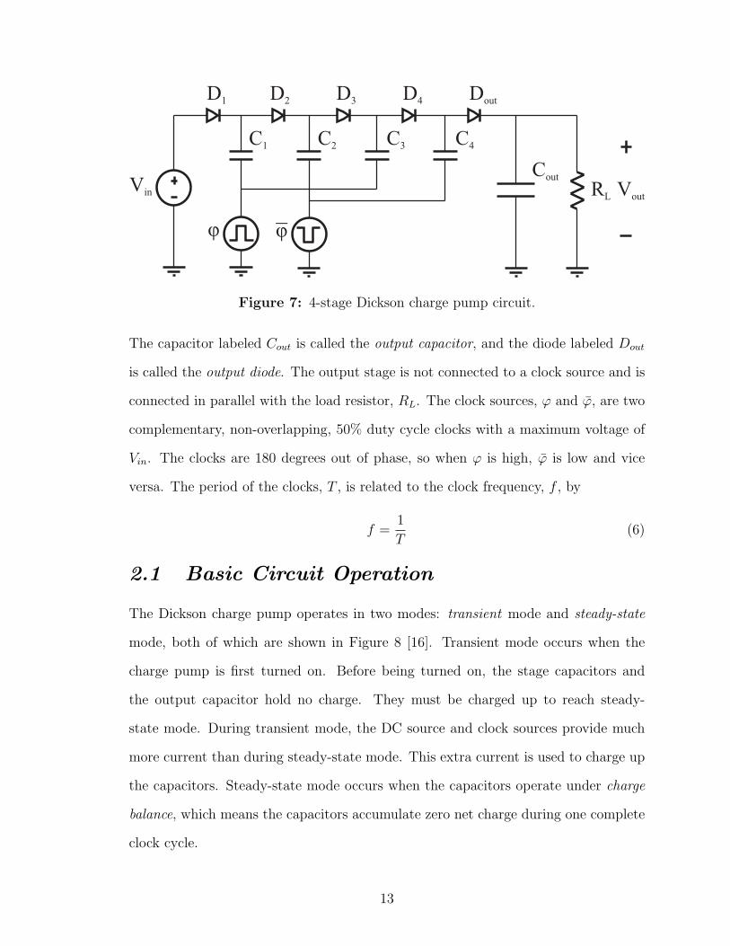
Figure 7: 4-stage Dickson charge pump circuit.
The capacitor labeled Cout is called the output capacitor, and the diode labeled Dout
is called the output diode. The output stage is not connected to a clock source and is
connected in parallel with the load resistor, RL. The clock sources, ϕ and ϕ, are two
complementary, non-overlapping, 50% duty cycle clocks with a maximum voltage of
Vin. The clocks are 180 degrees out of phase, so when ϕ is high, ϕ is low and vice
versa. The period of the clocks, T , is related to the clock frequency, f , by
f =1
T(6)
2.1 Basic Circuit Operation
The Dickson charge pump operates in two modes: transient mode and steady-state
mode, both of which are shown in Figure 8 [16]. Transient mode occurs when the
charge pump is first turned on. Before being turned on, the stage capacitors and
the output capacitor hold no charge. They must be charged up to reach steady-
state mode. During transient mode, the DC source and clock sources provide much
more current than during steady-state mode. This extra current is used to charge up
the capacitors. Steady-state mode occurs when the capacitors operate under charge
balance, which means the capacitors accumulate zero net charge during one complete
clock cycle.
13

Figure 8: Difference between transient and steady-state modes.
14

Pertinent equations such as input/output, power efficiency, input resistance, and
ripple voltage equations are given for the steady-state mode in the following subsec-
tions. Detailed derivations are given in Appendix A.
2.1.1 Input/Output Equation
The most common form of the input/output equation was first presented by John
F. Dickson [7]. For a general N -stage Dickson charge pump with clock voltage Vφ =
Vφ = Vin, this common output equation is
Vout = (N + 1)(Vin − Vt) −NIout
fC(7)
This form is derived in detail in appendix section A.1, but is then rearranged to a
simpler form:
Vout =(N + 1)(Vin − Vt)
1 + NfCRL
(8)
This equation describes how the output behaves when design parameters are changed.
Output voltage increases as more stages are added, but also loses Vt Volts as each stage
is added. The fractional term in the denominator, N/fCRL, is usually adds a small
amount to the denominator, which means changes in the number of stages, frequency,
capacitance, and load resistance do not affect the output voltage too heavily.
2.1.2 Power Efficiency
Power efficiency is defined as the ratio of power that makes it to the output without
getting dissipated vs. the power supplied. It can be calculated as
η =Pout
Pin
=VoutIout
VinIin
(9)
Efficiency η is easily found by substituting expressions for Vout, Iout, Vin, and Iin.
Appendix section A.3 derives these expressions in detail and makes substitutions into
equation (9). Two useful equations for power efficiency were derived. In terms of
15

input and output voltage, power efficiency is
η =Vout
Vin(N + 1)(10)
If only input voltage is known, the efficiency has the following dependencies:
η =(1 − Vt
Vin)
1 + NfCRL
(11)
These results have been verified through a different derivation technique by Tan-
zawa and Tanaka [23]. Equation (11) shows how the circuit parameters affect power
efficiency. Increasing frequency, stage capacitance, and load resistance all increase
efficiency as well as decreasing the number of stages. Efficiency becomes almost fre-
quency independent for f > N/(CRL). Efficiency depends on input voltage. For
large inputs, the Vt/Vin term is negligible, and efficiency becomes large. For small
inputs, the Vt/Vin term dominates, and efficiency becomes small. This circuit is only
useful for circuits with Vin > Vt.
The diodes are the only circuit components that dissipate power besides the load
resistor, and their threshold voltage is fairly constant for any diode current. Reducing
the current passing through the diodes for any given load resistance will increase
power efficiency. Large loads require less current than small loads for the same output
voltage. Large stage capacitors absorb less charge than small capacitors for constant
frequency. Reducing the number of stages reduces the number of diodes. All of these
things reduce the current through the diodes and increase power efficiency.
2.1.3 Output Ripple Voltage
The input/output equation gives a value for the maximum voltage the output can
be. Output ripple voltage determines how far the output voltage drops from the
final value given in equation (8). The load may require that voltage does not drop
below 95% of its specification. If it does, the load device may turn off, break, or do
something else that is undesired. So, it is important to determine what the output
ripple voltage will be based on circuit parameters.
16

From appendix section A.3, The expression for output voltage ripple is
∆Vout
Vout
=1
RLfCout
(12)
Ripple gets larger as load resistance gets smaller. Also, a faster frequency and a
larger output capacitance will suppress ripple. Let the specification for percent ripple
voltage be called α:
α =∆Vout
Vout
(13)
And let the ratio between output capacitance and stage capacitance be called β:
β =Cout
C(14)
Then, according to the detailed derivation in appendix section A.3 , β and α are
related by
β =1
RLfCα(15)
This relationship implies capacitor ratio, β, and the ripple voltage specification, α,
are inversely proportional to each other, which should make sense. Small ripple
implies small α, which implies large β and large output capacitance. A large load
resistance draws less charge from the output capacitor than a small load resistance,
so a small output capacitor would suffice. Increasing frequency decreases β also, so
along with the power efficiency equation (11), the designer can arbitrarily choose a
large frequency to minimize capacitor size and maximize efficiency.
2.1.4 Input Resistance
Input resistance describes the equivalent resistance seen looking into the circuit. It
is the same resistance the input solar cell array would see if connected to the input
of the charge pump. The input resistance determines how large or small the input
array needs to be in order to supply a certain input voltage and current.
17

Input resistance, Rin, is the resistance a Direct Current (DC) power source would
see if connected to the input of the Dickson charge pump. It is defined as
Rin =Vin
Iin
(16)
The expression for Iin is derived in appendix A section A.3 as
Iin = (N + 1)Iout (17)
Substituting this expression into equation (16) and then replacing Iout with Vout/RL,
equation (16) becomes
Rin =Vin
Iin
=Vin
(N + 1) Iout
=VinRL
(N + 1) Vout
(18)
Vin/Vout is the reciprocal of the the voltage gain, which is related simply to the power
efficiency by equation (10):
Vin
Vout
=1
η (N + 1)(19)
Substituting equation (19) into equation (18) yields
Rin =VinRL
(N + 1) Vout
=RL
η (N + 1)2(20)
This says input resistance decreases as the number of stages increases. This makes
sense because more stages means more current is drawn at the same voltage. Also,
load resistance determines the output current, which determines the input current as
well.
2.2 Dickson Charge Pump Design
This section will discuss the basic design of a Dickson charge pump, special design
cases, and the clock circuit used to drive the pump.
2.2.1 Basic Design
The common specifications for a DC-DC converter are:
18

• Output power
• Load resistance
• Input resistance
• Minimum power efficiency
• Percent ripple voltage
From these specifications, the designer must determine these circuit parameters:
• Stage diodes (threshold voltage)
• Number of stages
• Input power
• Input voltage
• Frequency
• Stage capacitance
• Output capacitance
The first parameter the designer must determine is the type of diode to use in
circuit. There is no equation or method that finds the perfect diode threshold voltage,
Vt, to use for the circuit. However, it will be shown later that low Vt minimizes the
size of the capacitors. So, the designer should choose diodes that are cheap and have
low Vt. Also, advanced techniques such as using body diode connections in silicon-
on-insulator (SOI) MOSFETs can be used. In some cases, this technique increases
power efficiency [12] [13], and it may be transferable to organic transistors as well.
19
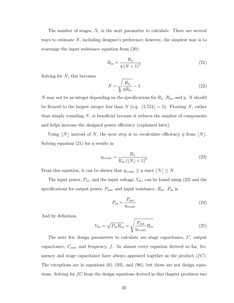
The number of stages, N , is the next parameter to calculate. There are several
ways to estimate N , including designer’s preference; however, the simplest way is to
rearrange the input resistance equation from (20):
Rin =RL
η (N + 1)2(21)
Solving for N , this becomes
N =
√
RL
ηRin
− 1 (22)
N may not be an integer depending on the specifications for RL, Rin, and η. N should
be floored to the largest integer less than N (e.g. ⌊5.724⌋ = 5). Flooring N , rather
than simply rounding N , is beneficial because it reduces the number of components
and helps increase the designed power efficiency (explained later).
Using ⌊N⌋ instead of N , the next step is to recalculate efficiency η from ⌊N⌋.
Solving equation (21) for η results in
ηrecalc =RL
Rin (⌊N⌋ + 1)2(23)
From this equation, it can be shown that ηrecalc ≥ η since ⌊N⌋ ≤ N .
The input power, Pin, and the input voltage, Vin, can be found using (23) and the
specifications for output power, Pout, and input resistance, Rin. Pin is
Pin =Pout
ηrecalc
(24)
And by definition,
Vin =√
PinRin =
√
Pout
ηrecalc
Rin (25)
The next few design parameters to calculate are stage capacitance, C, output
capacitance, Cout, and frequency, f . In almost every equation derived so far, fre-
quency and stage capacitance have always appeared together as the product (fC).
The exceptions are in equations (6), (93), and (96), but those are not design equa-
tions. Solving for fC from the design equations derived in this chapter produces two
20

Figure 9: Solution set for f and C. Most Dickson charge pump designs have large f(∼MHz) and small C (∼nF), because those are the typical sizes available.
equations:
fC =1
αβRL
(26)
fC =⌊N⌋
RL
[
ηrecalc
1 − ηrecalc −Vt
Vin
]
(27)
This is an under-determined system of equations, which produces infinite solutions
for f and C. The set of solutions for f and C form the graph shown in Figure 9.
Equation (27) will be used to determine the product (fC). Equation (27) contains
variables that were specified or found earlier in the design process, whereas equation
(26) contains β, which has not yet been found.
The set of infinite solutions, (f ,C), allows the designer the freedom to choose
f and C based on constraints such as component cost and size. Switch rise time
and fall time are factors that affect which frequency should be chosen [14]. Output
capacitance can be found using equation (26) and the equation for β in equation
21

(119). First β is found using
β =1
αfCRL
(28)
Then, Cout is found using
Cout = βC (29)
This finishes the basic design of the Dickson charge pump. The charge pump can
be designed for almost any combination of input resistance, power efficiency, load
resistance, and load power.
2.2.2 Special Cases
Sometimes, the constraint for η is too high for the given input resistance, and it is
simply impossible to build. In these situations, a sacrifice of power efficiency should
be made.
A large specification for η will sometimes call for N < 1. This situation occurs
when Rin is specified to be too large (Rin ≥ RL/η according to equation (22)). In
this case, the designer should simply set ⌊N⌋ = 1 in the design equations above.
Every specification can still be met except for the power efficiency: ηrecalc < η since
⌊N⌋ > N .
If the specifications call for a very small input voltage or a very high power ef-
ficiency, then the frequency-capacitance product will be negative (fC < 0). This
produces the inequality
ηrecalc +Vt
Vin
> 1 (30)
according to (27). The recalculated efficiency, ηrecalc, was recalculated from the speci-
fications, and input voltage, Vin, was found from the specifications. The only freedom
the designer has at this point is selection of a smaller Vt. If recalculated efficiency,
ηrecalc ≥ 1, then even letting Vt → 0 will not make fC positive. In this case, the de-
signer should take the ceiling of N , which is rounding upward to the smallest integer
22

Figure 10: φ and φ can be produced using a 555 timer and complementary inverter,or ”‘NOT”’ logic gate.
greater than N (e.g. ⌈5.724⌉ = 6). Using ⌈N⌉ will allow every specification to be met
except for power efficiency just as before: ηrecalc < η since ⌈N⌉ > N .
2.3 Clock Design
The two clock phases, φ and φ, can be designed in a number of ways. This section
discusses square-wave and sinusoidal clock designs.
2.3.1 Square-Wave Clock Design
A 555 timer chip is a circuit that can be configured to act as a 50% duty cycle switch
that flips between Vin and ground. The output pin of the 555 timer would be one phase
of the clock (φ). The other phase would be made using a complementary inverter with
φ as the input and φ as the output. This is a standard complementary inverter, or
“NOT” gate, where a “high” input produces a “low” output and vice-versa. Figure 10
shows this clock circuit.
Another option for the clock signal generator is a ring oscillator, which consists of
a NAND gate followed by an even number of NOT gates [25]. The output of the last
23
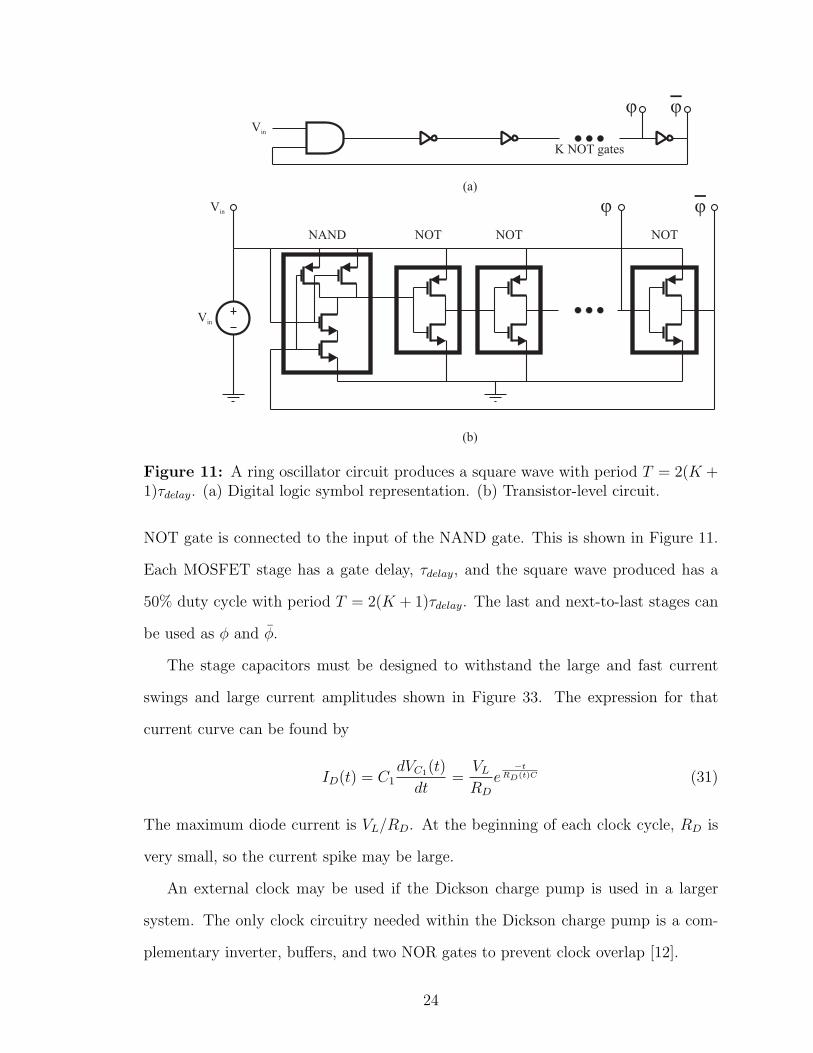
Figure 11: A ring oscillator circuit produces a square wave with period T = 2(K +1)τdelay. (a) Digital logic symbol representation. (b) Transistor-level circuit.
NOT gate is connected to the input of the NAND gate. This is shown in Figure 11.
Each MOSFET stage has a gate delay, τdelay, and the square wave produced has a
50% duty cycle with period T = 2(K + 1)τdelay. The last and next-to-last stages can
be used as φ and φ.
The stage capacitors must be designed to withstand the large and fast current
swings and large current amplitudes shown in Figure 33. The expression for that
current curve can be found by
ID(t) = C1
dVC1(t)
dt=
VL
RD
e−t
RD(t)C (31)
The maximum diode current is VL/RD. At the beginning of each clock cycle, RD is
very small, so the current spike may be large.
An external clock may be used if the Dickson charge pump is used in a larger
system. The only clock circuitry needed within the Dickson charge pump is a com-
plementary inverter, buffers, and two NOR gates to prevent clock overlap [12].
24

2.3.2 Sinusoidal Clock Design
If a sinusoidal clock is desired instead of a square-wave clock, the designer could choose
a crystal oscillator or any type of harmonic oscillator (Armstrong, Hartley, Colpitts,
etc.). The circuit connections need to be modified as in Figure 12a. Instead of a
separate φ-phase clock source connected to the even-numbered stages, these stages are
simply connected to ground. This method works because charge is transferred from
the even-numbered stages to the odd-numbered stages when the sinusoidal clock signal
goes negative. So, the charge transfer action of the charge pump is still preserved
even with a sinusoidal clock.
There are two benefits from using a sinusoidal clock over a square-wave clock.
First, the sinusoidal clock imposes a gradual voltage change across the capacitors,
which induces softer current transfer between the capacitors. The current no longer
looks like unit-step decaying exponential functions with large current spikes as in
Figure 33. Instead, the current looks like the curve in Figure 12b. In that graph, the
maximum current can be found by comparing IC(t) to a triangular approximation as
in the graph. The areas under IC(t) and the triangle curve must both be equal to
charge transferred, QL:
QL =1
2tLImax =
∫
tL
IC(t)dt = CVL (32)
Then, Imax is found as
Imax =2CVL
tL(33)
Making the substitution for VL using (104), this becomes
Imax =2Iout
ftL(34)
where
tL ∝Vin
fVout
(35)
25

Figure 12: (a) Dickson charge pump with sinusoidal clock phases. (b) Clock andstage capacitor voltage and current curves.
26

Figure 13: A VCO can provide output voltage regulation.
If the designer wishes to have control over the output voltage, a voltage-controlled
oscillator (VCO) could be used. A VCO can be used in a control loop as shown in
Figure 13 to regulate the output voltage in case the input voltage is not outputting
a constant average DC voltage. The plant is the Dickson charge pump, which has a
nonlinear gain with respect to frequency. Addition of a nonlinear control circuit would
then provide voltage regulation. The VCO may be used in either the square-wave
clock case or sinusoidal clock case.
Control over the output is useful when the input source experiences a sudden loss
or gain in power. For solar cell arrays, this means partial shading or unusually high
or low sun radiation, which causes a change in input voltage. The control system
may need to be powered by a separate, more reliable power source to provide reliable
reference voltages.
27

APPENDIX A
DICKSON CHARGE PUMP THEORY
A.1 Input/Output Equation Derivation
The circuit’s operation may be easily understood by analyzing the performance during
steady-state mode. Figure 32 shows the circuit from Figure 7 operating during the
two clock phases, the T/2 period when φ(t) is high and the T/2 period when φ(t) is
high. During φ, stage capacitor C1 is being charged by the input DC source, Vin. A
voltage loop equation will show that the expression for the voltage across C1 is
VC1 (t) = (Vin − VD1(t)) −[
(Vin − VD1(t)) − VC1
(
φbegin
)]
e−t
RD1(t)C1 (93)
where VD1(t) is the diode voltage, VC1
(
φbegin
)
is the voltage of capacitor C1 at the
beginning of the φ-phase, and RD1(t) is the on-resistance of diode D1. VD1(t) is
dependent on the diode current. For this analysis, we will assume that the current
through every diode is within ranges that allow VD1(t) ≈ Vt, where Vt is the diode
threshold voltage. The term VC1
(
φbegin
)
is equal to the voltage at the end of the
φ-phase, VC1(φend). It is also true that VC1(φbegin) = VC1
(
φend
)
. These relationships
hold for every capacitor in the circuit. RD1(t) is found by taking the ratio of its
voltage and current.
RD1(t) =VD1(t)
ID1(t)≈
Vt
ID1(t)(94)
This is the same as the reciprocal of the slope to the diode’s IV curve. RD1(t)
changes with current according to the diode equation. During the φ-phase, ID1(t) is
decreasing exponentially as shown in Figure 33, and VD1(t) decreases exponentially
with the same time constant but much more slowly. It stays approximately equal to
the threshold voltage of the diode. This implies RD1(t) is increasing almost linearly.
72

Figure 32: 4-Stage Dickson charge pump operating during (a) φ-phase and (b)φ-phase.
73

Figure 33: C1 voltage and current and D1 in steady-state.
When the φ-phase is just beginning, the capacitor draws a large amount of current,
which makes the on-resistance very low. By the end of the φ-phase, most of the charge
has been transferred to the capacitor, and the current drops to a low value, which
makes the on-resistance high. Most silicon diodes have on-resistances in the range of
1 and 1000 mΩ [18]. This dynamic resistance behavior is shown in Figure 33.
We will assume that the clock period is long enough to allow the approximation
VC1
(
φend
)
≈ VC1(t → ∞) = Vin − Vt (95)
At the beginning of the next clock phase (shown in Figure 32a), the capacitor voltage
should be continuous so that VC1(φbegin) = VC1(φend). The voltage presented to C2
is the sum of Vin, VC1(φbegin) and −Vt. At this point, VC2 is less than the sum of
74
these voltages, which means it begins to draw current (ID in Figure 32a) from the
input source. C1 loses charge as ID flows into C2 and away from C1, which means VC1
decreases and VC2 increases. The amount of charge lost from C1 and gained by C2 is
QL =
∫ φend
φbegin
ID(t)dt = C1VL (96)
where VL is the voltage lost (or transferred) from C1 to C2 and the charge-voltage
relationship Q = CV was used. The integral equation is simply the area under the
ID(t) curve in Figure 33. At the end of the φ-phase, VC1 has decreased to
VC1(φend) = VC1(φbegin) − VL = Vin − Vt − VL (97)
as shown in Figure 33. And since C2 can only charge up to the voltage to which it is
excited, its end-of-stage value is given by
VC2(φend) = Vin + VC1(φend) − Vt = 2(Vin − Vt) − VL (98)
The process of analysis gets repetitive after this point. For the next phase, the
capacitor voltage is continuous so that φ, VC2(φbegin) = VC2(φend). The circuit is in
steady-state, so the charge gained by C2, which is QL, during the φ-phase must be
lost during the φ-phase. So, the same current ID flows away from C2 and into C3,
taking QL away from C2 and into C3. At the end of the φ-phase, VC2 has dropped to
VC2(φend) = VC2(φbegin) − VL = 2(Vin − Vt) − 2VL (99)
And since C3 can only charge up to the voltage to which it is excited, its end-of-stage
value is given by
VC3(φend) = Vin + VC2(φend) − Vt = 3(Vin − Vt) − 2VL (100)
The same process can be carried out for the kth stage, and in general the voltage
across the kth stage capacitor, Ck, after φ (for even k) or φ (for odd k) is
VCk(φend or φend) = Vin + VCk−1
(φend or φend) − Vt = k(Vin − Vt) − (k − 1)VL (101)
75
This equations shows how the voltage across the stage capacitors increases with the
number of stages. The 4th stage capacitor will have approximately four times the
voltage of the 1st stage capacitor. The designer should choose capacitors that can
withstand this maximum voltage. This characteristic of the Dickson charge pump
makes it difficult to design for extremely high voltages such as 800 kV as in the
Cockcroft-Walton voltage multiplier.
The output capacitor in Figure 32 is charged during the φ-phase in the same way
that the other stage capacitors are charged. The final equation for Vout can be found
if Cout is viewed as a 5th stage capacitor.
Vout = VC5(φend) = Vin + VC4(φend) − Vt = 5(Vin − Vt) − 4VL (102)
This expression provides Vout, but the VL term is still present, which will depend on
the load resistance.
The output current can be found by analyzing charge transfer. Capacitor C4 loses
charge QL, which is gained by Cout. The charge gained by Cout during φ will be
discharged into the resistor during φ and φ because the resistor is always drawing
current regardless of the clocks’ phase. Since the circuit is operating in steady-state,
the charge gained by Cout must be discharged before the next clock cycle. This implies
that QL Coulombs is discharged by the load resistor during T seconds. This gives an
expression for output current:
Iout =QL
T(103)
By substituting equations (6) and (96), Iout can be expressed as
Iout = fC1VL (104)
Now, equation (102) can be improved by using equation (104) to substitute for VL in
equation (102), which becomes
Vout = 5(Vin − Vt) − 4Iout
fC1
(105)
76

This is the common output equation given for a 4-stage Dickson charge pump [7]
[29], but it is not in proper form because of the Iout term that appears on the right
hand side. If Iout is replaced with Vout/RL and C1 replaced with a common stage
capacitance, C, then equation (105) becomes
Vout = 5(Vin − Vt) − 4Vout
fCRL
(106)
Then, Vout can be solved as
Vout =5(Vin − Vt)
1 + 4
fCRL
(107)
This form of the equation is more proper and simpler than equation (105).
For a general N -stage Dickson charge pump with clock voltage Vφ = Vφ = Vin,
the output equation is
Vout =(N + 1)(Vin − Vt)
1 + NfCRL
(108)
This equation describes how the output behaves when design parameters are changed.
This form of the output equation will be used in the research.
A.2 Power Efficiency Derivation
Power efficiency is defined as the ratio of output power to input power:
η =Pout
Pin
=VoutIout
VinIin
(109)
Efficiency η is found by substituting expressions for Vout, Iout, Vin, and Iin.
The output voltage equation was derived in Section 2.1, equation (108). The
output current equation was derived in Section 2.1, equation (104), and was found to
be
Iout =QL
T= fCVL = fCout∆Vout (110)
which has units Coulombs/Second or Amperes as expected.
Figure 32 is helpful in explaining the derivation of steady-state input current to
the charge pump. Figure 33 shows the DC input source five times: once as the DC
77
input, and four times as a replacement for the clock sources. The input source supplies
current ID five times during once complete clock cycle. And since QL is defined by
QL =
∫ φend
φbegin
ID(t)dt (111)
it must be true that the total charge supplied by the input source during one complete
clock cycle is
Qin =
∫ φend
φbegin
5ID(t)dt = 5
∫ φend
φbegin
ID(t)dt = 5QL (112)
Equations (111) and (112) were derived for a four-stage Dickson charge pump, so it
makes sense that for an N -stage Dickson charge pump, the charge injected by the
input source is
Qin = (N + 1)QL (113)
Input current Iin can be found using (113) and (110) as
Iin =Qin
T= (N + 1)
QL
T= (N + 1)Iout (114)
Now, Vout, Iout, and Iin are all clearly expressed in terms of Dickson charge pump
circuit parameters. Equation (108) is augmented to formulate the power efficiency, η:
Vout
Vin
=(N + 1)(1 − Vt
Vin)
1 + NfCRL
(115)
Now, multiplying (115) by Iout/Iin gives power efficiency as
η =Vout
Vin
Iout
Iin
=Vout
Vin
Iout
(N + 1)Iout
=Vout
Vin
1
(N + 1)=
(1 − Vt
Vin)
1 + NfCRL
(116)
These two forms of the efficiency equation are useful at different stages of the design
process. If the efficiency is specified, then equation (115) is used to find the input
voltage. Then, equation (116) is used to find other circuit components like frequency,
stage capacitance, or diode threshold voltage.
78

A.3 Output Voltage Ripple Derivation
The output capacitor usually has different capacitance than the stage capacitors be-
cause it directly influences the magnitude of the output ripple voltage, ∆Vout, whereas
the stage capacitors directly influence Vout. Stage capacitance does affect ripple volt-
age indirectly. It is primarily chosen control output voltage. Cout is commonly de-
signed to be large in order to reduce output ripple voltage. The difference in capacitor
size affects the voltage gained by Cout during charge transfer. The relationship be-
tween ∆Vout and VL is found by equating charge lost by the last stage capacitor with
capacitance C and charge gained by Cout.
QL = CVL = Cout∆Vout (117)
⇒ ∆Vout =C
Cout
VL (118)
The ratio of capacitor size is an important design parameter because it affects the size
of the output ripple voltage. The ratio of output capacitance to stage capacitance is
called β, and is defined as
β =Cout
C(119)
Also, percent ripple voltage, or ∆Vout/Vout is a common specification for the output
of a DC to DC converter. The percent ripple voltage is called α, and is defined as
α =∆Vout
Vout
(120)
Equation (118) can be modified using equations (110), (119), and (120) to get a
relationship between the ripple voltage specification, α, and the ratio of capacitance,
β. First, equation (118) is rearranged to be
Cout
C=
VL
∆Vout
(121)
Then, a substitution for VL is made, resulting in
Cout
C=
Iout
fC∆Vout
(122)
79

Then, using Ohm’s Law to replace Iout, (122) becomes
Cout
C=
Vout
RLfC∆Vout
(123)
Finally, the substitutions for β and α are made resulting in
β =1
RLfCα(124)
Then, the expression for output voltage ripple is
α =∆Vout
Vout
=1
RLfCout
(125)
80
The pair of ones within the parenthesis cancel, and this equation can be rearranged
in terms of powers of VOC :
0 = IPH −
(
ISβv +1
RP
)
VOC −
(
IS
β2v
2!
)
V 2OC −
(
IS
β3v
3!
)
V 3OC − . . . (136)
Then, multiplying by −1 and dividing by IS gives a simpler form of the polynomial
0 = −IPH
IS
+
(
βv +1
ISRP
)
VOC +β2
v
2!V 2
OC +β3
v
3!V 3
OC + . . . (137)
VOC can be approximated by truncating this infinite-degree polynomial to a large, but
finite-degree polynomial just like in the method for solving for ISC . Then, a computer
program like MATLAB can solve the equation quickly. From this equation, we can
see that VOC is dependent on IPH , IS, and βv, which is dependent on ideality factor,
n, and temperature, T . VOC is only slightly dependent on RP .
83

REFERENCES
[1] Baderna, D., Cabrini, A., and Torelli, G., “Efficiency comparison between
doubler and dickson charge pumps,” IEEE, vol. 89, pp. 1891–1894, December
2005.
[2] Bouhamame, M., Tourret, J. R., Coco, L. L., Toutain, S., and
Pasquier, O., “A fully intergrated DC/DC converter for tunable RF filters,”
in IEEE 2006 Custom Intergrated Circuits Conference, pp. 817 – 820, 10 - 13
September 2006.
[3] Cabrini, A., Gobbi, L., and Torelli, G., “Theoretical and experimental
analysis of dickson charge pump output resistance,” in Proceedings of the IEEE
International Symposium on Circuits and Systems, pp. 2749 – 2752, 21 - 24 May
2006.
[4] Cockcroft, F. D. and Walton, E. T., “Production of high velocity positive
ions.,” Proceedings of the Royal Society of London. Series A, Containing Papers
of a Mathematical and Physical Character, vol. 136, pp. 619–630, June 1932.
[5] Council of Economic Advisers, Economic Report of the President with The
Annual Report of the Council of Economic Advisers. Washington, D.C.: United
States Government Printing Office, 2008.
[6] Cuk, S. and Middlebrook, R. D., “A new optimum topology switching dc-
to-dc converter,” in Power Electronics Specialists Conference, 1977.
84

[7] Dickson, J. F., “On-chip high-voltage generation in MNOS integrated circuits
using an improved voltage multiplier technique,” IEEE Journal of Solid-State
Circuits, vol. SC-11, pp. 374–378, June 1976.
[8] Forrest, S., “The Limits to Organic Photovoltaic Cell Efficiency,” MRS Bul-
letin, vol. 30, pp. 28 – 32, January 2005.
[9] Garg, H. P. and Mullick, S. C. and Bhargava, A. K., Solar Thermal
Energy Storage. Springer, 1985.
[10] Green, M. A., Emery, K., King, D., Hishikawa, Y., and Warta, W., “So-
lar cell efficiency tables,” Progress in Photovoltaics: Research and Applications,
vol. 15, pp. 35 – 40, December 2006.
[11] Hoppe, H. and Niyazi, S. S., “Organic solar cells: an overview,” Journal of
Materials Research, vol. 19, pp. 1924 – 1945, March 2004.
[12] Hoque, M., Ahmad, T., McNutt, T. R., Mantooth, H. A., and Mo-
jarradi, M. M., “A technique to increase the efficiency of high-voltage charge
pumps.,” IEEE Transactions on Circuits and Systems, vol. 53, pp. 364 – 368,
May 2006.
[13] Hoque, M., McNutt, T., Zhang, J., Mantooth, A., and Mojarradi,
M., “A high-voltage dickson charge pump in SOI CMOS,” in Proceedings of
the IEEE 2003 Custom Integrated Circuits Conference, pp. 493 – 496, 21 - 24
September 2003.
[14] Liu, L. and Chen, Z., “Analysis and design of makowski charge-pump cell,”
in 6th International Conference on ASIC, vol. 1, pp. 497 – 502, 23 - 26 October
2005.
85
[15] Luque, A. and Hegedus, S., Handbook of Photovoltaic Science and Engineer-
ing. John Wiley and Sons, Inc., 2003.
[16] Mohan, N., Undeland, T. M., and Robbins, W. P., Power Electronics.
John Wiley and Sons, Inc., 2003.
[17] Nakayashiki, K., “Understanding og defect passivation and its effect on mul-
ticrystalline silicon solar cell performance.,” doctoral thesis, Georgia Institute of
Technology, 2001. Online: http://smartech.gatech.edu/handle/1853/19854.
[18] NXP, PMEG6010CEH; PMEG6010CEJ A very low VF MEGA schottky barrier
rectifiers, 2007.
[19] Peumans, P., Bulovi, V., and Forrest, S. R., “Efficient photon harvest-
ing at high optical intensities in ultrathin organic double-heterostructure photo-
voltaic diodes,” Applied Physics Letters, vol. 76, p. 2650 to 2652, May 2000.
[20] Poortmans, J. and Arkhipov, V., Thin Film Solar Cells: Fabrication, Char-
acterization and Applications. John Wiley and Sons, Inc., 2006.
[21] Shah, A., Torres, P., Tscharner, R., Wyrsch, N., and Keppner, H.,
“Photovoltaic technology: the case for thin-film solar cells,” in Science Magazine,
vol. 285, pp. 692–698, 1999.
[22] Shaheen, S. E., Radspinner, R., Peyghambarian, N., and Jabbour,
G., “Fabrication of bulk heterojunction plastic solar cells by screen printing,”
Applied Physics Letters, vol. 79, pp. 2996 – 2998, October 2001.
[23] Tanzawa, T. and Tanaka, T., “A dynamic analysis of the dickson charge
pump circuit,” IEEE Journal of Solid-State Circuits, vol. 32, pp. 1231–1240,
August 1997.
86

[24] Vak, D., Kim, S., Jo, J., Oh, S., Na, S., Kim, J., and Kima, D., “Fabri-
cation of organic bulk heterojunction solar cells by a spray deposition method
for low-cost power generation,” Applied Physics Letters, vol. 79, pp. 081102–1 to
081102–3, August 2007.
[25] Wu, W. C., “On-chip charge pumps,” master’s thesis, Georgia Institute of Tech-
nology, 2001. Online: http://smartech.gatech.edu/dspace/handle/1853/13451.
[26] Yoo, C. and Lee, K., “A low-ripple poly-Si TFT charge pump for driver-
integrated LCD panel,” IEEE Transactions on Consumer Electronics, vol. 51,
pp. 606 – 610, May 2005.
[27] Yoo, S., Domercq, B., and Kippelen, B., “Intensity-dependent equivalent
circuit parameters of organic solar cells based on pentacene and C60,” Journal
of Applied Physics, vol. 97, pp. 103706–1 to 103706–9, May 2005.
[28] Yoo, S., Potscavage, W. J., Domercq, B., Kim, J., Holt, J., and Kip-
pelen, B., “Integrated organic photovoltaic modules with a scalable voltage
output,” Applied Physics Letters, vol. 89, pp. 233516–1 to 233516–3, December
2006.
[29] Zhang, M. and Llaser, N., “Optimization design of the dickson charge pump
circuit with a resistive load,” in Proceedings of the 2004 International Symposium
on Circuits and Subsystems, vol. 5, pp. V–840 – V–843, 23 - 26 May 2004.
87