1.2 a/1.25 mhz, high-efficiency step-down converter … · tps62040 tps62042, tps62043 tps62044,...
TRANSCRIPT
TPS62040TPS62042, TPS62043TPS62044, TPS62046
SLVS463B − JUNE 2003 − REVISED OCTOBER 2005
1.2 A/1.25 MHz, HIGH-EFFICIENCY STEP-DOWN CONVERTER
FEATURES Up to 95% Conversion Efficiency
Typical Quiescent Current: 18 µA
Load Current: 1.2 A
Operating Input Voltage Range: 2.5 V to 6.0 V
Switching Frequency: 1.25 MHz
Adjustable and Fixed Output Voltage
Power Save Mode Operation at Light loadCurrents
100% Duty Cycle for Lowest Dropout
Internal Softstart
Dynamic Output Voltage Positioning
Thermal Shutdown
Short-Circuit Protection
10 Pin MSOP PowerPad™ Package
10 Pin QFN 3 X 3 mm Package
APPLICATIONS PDA, Pocket PC and Smart Phones
USB Powered Modems
CPUs and DSPs
PC Cards and Notebooks
xDSL Applications
Standard 5-V to 3.3-V Conversion
DESCRIPTION
The TPS6204x family of devices are high efficiencysynchronous step-down dc-dc converters optimized forbattery powered portable applications. The devices areideal for portable applications powered by a single Li-Ionbattery cell or by 3-cell NiMH/NiCd batteries. With anoutput voltage range from 6.0 V down to 0.7 V, the devicessupport low voltage DSPs and processors in PDAs,pocket PCs, as well as notebooks and subnotebookcomputers. The TPS6204x operates at a fixed switchingfrequency of 1.25 MHz and enters the power save modeoperation at light load currents to maintain high efficiencyover the entire load current range. For low noiseapplications, the devices can be forced into fixedfrequency PWM mode by pulling the MODE pin high. TheTPS6204x supports up to 1.2-A load current.
7VIN
VINEN
MODE
SW
FB
PGND
PGND
SW
GND
2
31
4 9
10
5
8
6
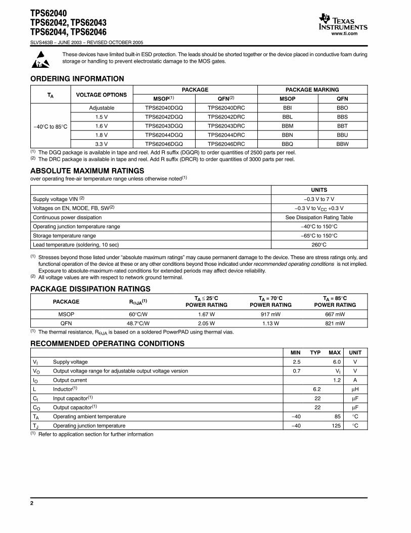
TPS6204xVI2.5 V to 6 V
VO0.7 V to VI /1.2 A
C222 µF
C122 µF
L16.2 µH
Typical Application Circuit 1.2-A Output Current
40
45
50
55
60
65
70
75
80
85
90
95
100
0 0.01 0.1 1 10 100 1 k 10 k
VI = 2.7 V
VI = 3.6 V
VI = 5 V
MODE = Low
VI = 3.6 VMODE = High
Eff
icie
ncy
− %
EFFICIENCYvs
LOAD CURRENT
IL − Load Current − mA
VO = 1.8 V
PRODUCTION DATA information is current as of publication date. Productsconform to specifications per the terms of Texas Instruments standard warranty.Production processing does not necessarily include testing of all parameters.
Please be aware that an important notice concerning availability, standard warranty, and use in critical applications of Texas Instrumentssemiconductor products and disclaimers thereto appears at the end of this data sheet.
www.ti.com
Copyright © 2003 − 2005, Texas Instruments Incorporated
PowerPAD is a trademark of Texas Instruments.
TPS62040TPS62042, TPS62043TPS62044, TPS62046SLVS463B − JUNE 2003 − REVISED OCTOBER 2005
www.ti.com
2
These devices have limited built-in ESD protection. The leads should be shorted together or the device placed in conductive foam duringstorage or handling to prevent electrostatic damage to the MOS gates.
ORDERING INFORMATION
T VOLTAGE OPTIONSPACKAGE PACKAGE MARKING
TA VOLTAGE OPTIONSMSOP(1) QFN(2) MSOP QFN
Adjustable TPS62040DGQ TPS62040DRC BBI BBO
1.5 V TPS62042DGQ TPS62042DRC BBL BBS
−40°C to 85°C 1.6 V TPS62043DGQ TPS62043DRC BBM BBT40 C to 85 C
1.8 V TPS62044DGQ TPS62044DRC BBN BBU
3.3 V TPS62046DGQ TPS62046DRC BBQ BBW(1) The DGQ package is available in tape and reel. Add R suffix (DGQR) to order quantities of 2500 parts per reel.(2) The DRC package is available in tape and reel. Add R suffix (DRCR) to order quantities of 3000 parts per reel.
ABSOLUTE MAXIMUM RATINGSover operating free-air temperature range unless otherwise noted(1)
UNITS
Supply voltage VIN (2) −0.3 V to 7 V
Voltages on EN, MODE, FB, SW(2) −0.3 V to VCC +0.3 V
Continuous power dissipation See Dissipation Rating Table
Operating junction temperature range −40°C to 150°C
Storage temperature range −65°C to 150°C
Lead temperature (soldering, 10 sec) 260°C
(1) Stresses beyond those listed under “absolute maximum ratings” may cause permanent damage to the device. These are stress ratings only, andfunctional operation of the device at these or any other conditions beyond those indicated under recommended operating conditions is not implied.Exposure to absolute-maximum-rated conditions for extended periods may affect device reliability.
(2) All voltage values are with respect to network ground terminal.
PACKAGE DISSIPATION RATINGS
PACKAGE RJA(1) TA ≤ 25°CPOWER RATING
TA = 70°CPOWER RATING
TA = 85°CPOWER RATING
MSOP 60°C/W 1.67 W 917 mW 667 mW
QFN 48.7°C/W 2.05 W 1.13 W 821 mW(1) The thermal resistance, RΘJA is based on a soldered PowerPAD using thermal vias.
RECOMMENDED OPERATING CONDITIONSMIN TYP MAX UNIT
VI Supply voltage 2.5 6.0 V
VO Output voltage range for adjustable output voltage version 0.7 VI V
IO Output current 1.2 A
L Inductor(1) 6.2 µH
CI Input capacitor(1) 22 µF
CO Output capacitor(1) 22 µF
TA Operating ambient temperature −40 85 °C
TJ Operating junction temperature −40 125 °C(1) Refer to application section for further information

TPS62040TPS62042, TPS62043TPS62044, TPS62046
SLVS463B − JUNE 2003 − REVISED OCTOBER 2005
www.ti.com
3
ELECTRICAL CHARACTERISTICS VI = 3.6 V, VO = 1.8 V, IO = 600 mA, EN = VIN, TA = −40°C to 85°C, typical values are at TA = 25°C (unless otherwise noted)(1)
SUPPLY CURRENT
PARAMETER TEST CONDITIONS MIN TYP MAX UNIT
VI Input voltage range 2.5 6.0 V
I(Q) Operating quiescent current IO = 0 mA, device is not switching 18 35 µA
ISD Shutdown supply current EN = GND 0.1 1 µA
VUVLO Under−voltage lockout threshold 1.5 2.3 V
ENABLE AND MODE
VEN EN high level input voltage 1.4 V
VEN EN low level input voltage 0.4 V
IEN EN input bias current EN = GND or VIN 0.01 1.0 µA
V(MODE) MODE high level input voltage 1.4 V
V(MODE) MODE low level input voltage 0.4 V
I(MODE) MODE input bias current MODE = GND or VIN 0.01 1.0 µA
POWER SWITCH
rP-channel MOSFET on−resistance VI = VGS = 3.6 V 115 210 mΩ
rDS(ON) P-channel MOSFET on−resistance VI = VGS = 2.5 V 145 270 mΩ
Ilkg(P) P-channel leakage current VDS = 6.0 V 1 µA
rN-channel MOSFET on−resistance VI = VGS = 3.6 V 85 200 mΩ
rDS(ON) N-channel MOSFET on−resistance VI = VGS = 2.5 V 115 280 mΩ
IIkg(N) N-channel leakage current VDS = 6.0 V 1 µA
IL P-channel current limit 2.5 V < VI< 6.0 V 1.5 1.85 2.2 A
Thermal shutdown 150 °C
OSCILLATOR
f Oscillator frequencyVFB = 0.5 V 1 1.25 1.5 MHz
fS Oscillator frequencyVFB = 0 V 625 kHz
OUTPUT
VO Adjustable output voltage range TPS62040 0.7 VIN V
Vref Reference voltage 0.5 V
VFB Feedback voltageTPS62040Adjustable
VI = 2.5 V to 6.0 V; IO= 0 mAVI = 2.5 V to 6.0 V; 0 mA ≤ IO ≤ 1.2 A
0%
−3%
3%
3%
TPS620421.5V
VI = 2.5 V to 6.0 V; IO = 0 mAVI = 2.5 V to 6.0 V; 0 mA ≤ IO ≤ 1.2 A
0%
−3%
3%
3%
V Fixed output voltage
TPS620431.6V
VI = 2.5 V to 6.0 V; IO = 0 mAVI = 2.5 V to 6.0 V; 0 mA ≤ IO ≤ 1.2 A
0%
−3%
3%
3%VO Fixed output voltage
TPS620441.8V
VI = 2.5 V to 6.0 V; IO = 0 mAVI = 2.5 V to 6.0 V; 0 mA ≤ IO ≤ 1.2 A
0%
−3%
3%
3%
TPS620463.3V
VI = 3.6 V to 6.0 V; IO = 0 mAVI = 3.6 V to 6.0 V; 0 mA ≤ IO ≤ 1.2 A
0%
−3%
3%
3%
Line regulation(1) VI = VO + 0.5 V (min. 2.5 V) to 6.0 V,IO = 10 mA
0 %/V
Load regulation(1) IO = 10 mA to 1200 mA 0 %/mA
ILeakage current into SW pin VI>VO, 0 V ≤ Vsw ≤ VI 0.1 1 µA
IIkg(SW) Reverse leakage current into pin SW VI = open; EN = GND; VSW = 6.0 V 0.1 1 µA
f Short circuit switching frequency VFB = 0 V 625 kHz(1) The line and load regulations are digitally controlled to assure an output voltage accuracy of ±3%.

TPS62040TPS62042, TPS62043TPS62044, TPS62046SLVS463B − JUNE 2003 − REVISED OCTOBER 2005
www.ti.com
4
PIN ASSIGNMENTS
1
2
3
4
5
10
9
8
7
6
ENVINVIN
GNDFB
PGNDPGNDSWSWMODE
DGQ PACKAGE(TOP VIEW)
NOTE: The PowerPAD must be connected to GND.
1
2
3
4
5
10
9
8
7
6
ENVIN
VINGND
FB
PGNDPGND
SWSWMODE
DRC PACKAGE(TOP VIEW)
Terminal Functions
TERMINALI/O DESCRIPTION
NAME NO.I/O DESCRIPTION
EN 1 I Enable. Pulling EN to ground forces the device into shutdown mode. Pulling EN to VI enables the device. EN shouldnot be left floating and must be terminated.
VIN 2,3 I Supply voltage input
GND 4 Analog ground
FB 5 I Feedback pin. Connect FB directly to the output if the fixed output voltage version is used. For the adjustable versionan external resistor divider is connected to this pin. The internal voltage divider is disabled for the adjustable version.
MODE 6 I Pulling the MODE pin high allows the device to be forced into fixed frequency operation. Pulling the MODE pin to lowenables the power save mode where the device operates in fixed frequency PWM mode at high load currents andin PFM mode (pulse frequency modulation) at light load currents.
SW 7,8 I/O This is the switch pin of the converter and is connected to the drain of the internal power MOSFETs
PGND 9,10 Power ground

TPS62040TPS62042, TPS62043TPS62044, TPS62046
SLVS463B − JUNE 2003 − REVISED OCTOBER 2005
www.ti.com
5
FUNCTIONAL BLOCK DIAGRAM
FB PGND
SW
VIN
EN
UndervoltageLockout
Bias supply
Control Logic
+
−
LoadComparator
1.25 MHzOscillator
Vref = 0.5 V
DriverShoot−thru
Logic
P−C
han
nel
Po
wer
MO
SF
ET
N−C
han
nel
Po
wer
MO
SF
ET
R1R2
SoftStart
+
−
+
−
Current limit Comparator
SkipComparator
Gm
Saw ToothGenerator
V
I
+
−
Vcomp
S
R
+−
Comp High
Comp Low
Comp Low 2
Comp High
Comp Low
Comp Low 2
−
+
Comparator
Compensation
Ref
Ref
PGND
VIN
GNDMODE
MODE
SW
For the Adjustable Version the FB Pin IsDirectly Connected to the Gm Amplifier

TPS62040TPS62042, TPS62043TPS62044, TPS62046SLVS463B − JUNE 2003 − REVISED OCTOBER 2005
www.ti.com
6
TYPICAL CHARACTERISTICS
TABLE OF GRAPHS
FIGURE
η Efficiency vs Load current 1, 2, 3
η Efficiency vs Input voltage 4
IQ Quiescent current vs Input voltage 5, 6
fs Switching frequency vs Input voltage 7
rDS(on) P-Channel rDS(on) vs Input voltage 8
rDS(on) N-Channel rectifier rDS(on) vs Input voltage 9
Load transient response 10
PWM operation 11
Power save mode 12
Start-up 13
Figure 1
40
45
50
55
60
65
70
75
80
85
90
95
100
0 0.01 0.1 1 10 100 1 k 10 k
VO = 3.3 V
VI = 3.6 VMODE = Low
VI = 5 VMODE = Low
VI = 3.6 VMODE = High
VI = 5 VMODE = High
Eff
icie
ncy
− %
EFFICIENCYvs
LOAD CURRENT
IL − Load Current − mA
Figure 2
40
45
50
55
60
65
70
75
80
85
90
95
100
0 0.01 0.1 1 10 100 1 k 10 k
VO = 1.8 V
VI = 2.7 V
VI = 3.6 V
VI = 5 V
MODE = Low
VI = 3.6 VMODE = High
Eff
icie
ncy
− %
EFFICIENCYvs
LOAD CURRENT
IL − Load Current − mA

TPS62040TPS62042, TPS62043TPS62044, TPS62046
SLVS463B − JUNE 2003 − REVISED OCTOBER 2005
www.ti.com
7
Figure 3
40
45
50
55
60
65
70
75
80
85
90
95
100
0 0.01 0.1 1 10 100 1 k 10 k
VO = 1.5 V
VI = 2.7 V
VI = 3.6 V
VI = 5 V
Eff
icie
ncy
− %
EFFICIENCYvs
LOAD CURRENT
IL − Load Current − mA
Figure 4
70
75
80
85
90
95
100
2.5 3 3.5 4 4.5 5 5.5 6
VO = 1.8 VMODE = Low
IL = 500 mA
IL = 1000 mA
IL = 1 mA
Eff
icie
ncy
− %
EFFICIENCYvs
INPUT VOLTAGE
VI − Input Voltage − V
Figure 5
5
7
9
11
13
15
17
19
21
23
2.4 2.8 3.2 3.6 4 4.4 4.8 5.2 5.6 6
Qu
isec
ent C
urr
ent −
QUIESCENT CURRENTvs
INPUT VOLTAGE
VI − Input Voltage − V
Aµ
MODE = LowTA = 85°C
TA = 25°C
TA = −40°C
Figure 6
3
3.5
4
4.5
5
5.5
6
6.5
7
7.5
2.5 3 3.5 4 4.5 5 5.5 6
Qu
isec
ent C
urr
ent −
QUIESCENT CURRENTvs
INPUT VOLTAGE
VI − Input Voltage − V
mA
MODE = High
TA = 25°C

TPS62040TPS62042, TPS62043TPS62044, TPS62046SLVS463B − JUNE 2003 − REVISED OCTOBER 2005
www.ti.com
8
Figure 7
1.18
1.18
1.19
1.19
1.20
1.20
1.21
1.21
1.22
1.22
1.23
1.23
2.5 2.9 3.3 3.7 4.1 4.5 4.9 5.3 5.7 6
f − S
witc
hin
g F
req
uen
cy −
MH
z
SWITCHING FREQUENCYvs
INPUT VOLTAGE
VI − Input Voltage − V
TA = 85°C
TA = 25°C
TA = −40°C
Figure 8
2.5 2.9 3.3 3.7 4.1 4.5 4.9 5.3 5.7 6
P-CHANNEL rDS(on)vs
INPUT VOLTAGE
VI − Input Voltage − V
TA = 85°C
TA = 25°C
TA = −40°C
0.080
0.090
0.100
0.110
0.120
0.130
0.140
0.150
0.160
0.170
0.180
ΩD
S(o
n) −
P−C
han
nel
r
Figure 9
2.5 2.9 3.3 3.7 4.1 4.5 4.9 5.3 5.7 6
N-CHANNEL RECTIFIER rDS(on)vs
INPUT VOLTAGE
VI − Input Voltage − V
TA = 85°C
TA = 25°C
TA = −40°C
N-C
han
nel
Rec
tifi
er r
Ω
0.050
0.060
0.070
0.080
0.090
0.100
0.110
0.120
0.130
0.140
0.150
DS
(on
) −

TPS62040TPS62042, TPS62043TPS62044, TPS62046
SLVS463B − JUNE 2003 − REVISED OCTOBER 2005
www.ti.com
9
Figure 10
LOAD TRANSIENT RESPONSEI
50 µs/div
V OO
100
mV
/div
150m
A to
1.1
5 A
VI = 3.6 VVO = 1.8 VPWM/PFM Operation
Figure 11
PWM OPERATION
500 ns/div
VS
W5
V/d
iv
V O20
mV
/div
I L50
0 m
A/d
iv
Figure 12
POWER SAVE MODE
VS
W5
V/d
iv
V O20
mV
/div
I L50
0 m
A/d
iv
2.5 µs/div
Figure 13
START-UP
200 µs/div
En
able
2 V
/div
V O1
V/d
iv
I IN20
0 m
A/d
iv
VI = 3.6 VVO = 1.8 VIO = 1.1 A

TPS62040TPS62042, TPS62043TPS62044, TPS62046SLVS463B − JUNE 2003 − REVISED OCTOBER 2005
www.ti.com
10
DETAILED DESCRIPTION
OPERATION
The TPS6204x is a synchronous step-down converter operating with typically 1.25 MHz fixed frequency. At moderateto heavy load currents, the device operates in pulse width modulation (PWM), and at light load currents, the deviceenters power save mode operation using pulse frequency modulation (PFM). When operating in PWM mode, thetypical switching frequency is 1.25 MHz with a minimum switching frequency of 1 MHz. This makes the devicesuitable for xDSL applications minimizing RF (radio frequency) interference.
During PWM operation the converter uses a unique fast response voltage mode controller scheme with input voltagefeed−forward to achieve good line and load regulation, allowing the use of small ceramic input and output capacitors.At the beginning of each clock cycle initiated by the clock signal (S) the P-channel MOSFET switch turns on and theinductor current ramps up until the comparator trips and the control logic turns off the switch. The current limitcomparator also turns off the switch in case the current limit of the P-channel switch is exceeded. After the dead timepreventing current shoot through, the N-channel MOSFET rectifier is turned on and the inductor current ramps down.The next cycle is initiated by the clock signal, again turning off the N-channel rectifier and turning on the P-channelswitch.
The Gm amplifier as well as the input voltage determines the rise time of the saw tooth generator, and therefore, anychange in input voltage or output voltage directly controls the duty cycle of the converter, giving a very good line andload transient regulation.
POWER SAVE MODE OPERATION
As the load current decreases, the converter enters power save mode operation. During power save mode theconverter operates with reduced switching frequency in PFM mode and with a minimum quiescent currentmaintaining high efficiency.
The converter monitors the average inductor current and the device enters power save mode when the averageinductor current is below the threshold. The transition point between PWM and power save mode is given by thetransition current with the following equation:
Itransition VI
18.66
During power save mode the output voltage is monitored with the comparator by the threshold’s comp low and comphigh. As the output voltage falls below the comp low threshold set to typically 0.8% above the nominal output voltage,the P-channel switch turns on. The P-channel switch remains on until the transition current (1) is reached. Then theN-channel switch turns on completing the first cycle. The converter continues to switch with its normal duty cycledetermined by the input and output voltage but with half the nominal switching frequency of 625-kHz typ. Thus theoutput voltage rises and as soon as the output voltage reaches the comp high threshold of 1.6%, the converter stopsswitching. Depending on the load current, the converter switches for a longer or shorter period of time in order todeliver the energy to the output. If the load current increases and the output voltage can not be maintained with thetransition current , equation (1), the converter enters PWM again. See Figure 11 and Figure 12 under the typicalgraphs section and Figure 14 for power save mode operation. Among other techniques this advanced power savemode method allows high efficiency over the entire load current range and a small output ripple of typically 1% ofthe nominal output voltage.
Setting the power save mode thresholds to typically 0.8% and 1.6% above the nominal output voltage at light loadcurrent results in a dynamic voltage positioning achieving lower absolute voltage drops during heavy load transientchanges. This allows the converter to operate with small output capacitors like 22 µF and still having a low absolutevoltage drop during heavy load transient. Refer to Figure 14 as well for detailed operation of the power save mode.
(1)

TPS62040TPS62042, TPS62043TPS62044, TPS62046
SLVS463B − JUNE 2003 − REVISED OCTOBER 2005
www.ti.com
11
1.6%
0.8%
VO
Comp High
Comp Low
Comp Low 2
PWM Mode at Medium to Full Load
PFM Mode at Light Load
Figure 14. Power Save Mode Thresholds and Dynamic Voltage Positioning
The converter enters the fixed frequency PWM mode as soon as the output voltage falls below the comp low 2threshold.
DYNAMIC VOLTAGE POSITIONING
As described in the power save mode operation sections before and as detailed in Figure 14 the output voltage istypically 0.8% (i.e., 1% on average) above the nominal output voltage at light load currents, as the device is in powersave mode. This gives additional headroom for the voltage drop during a load transient from light load to full load.In the other direction during a load transient from full load to light load the voltage overshoot is also minimized byturning on the N-Channel rectifier switch to pull the output voltage actively down.
MODE (AUTOMATIC PWM/PFM OPERATION AND FORCED PWM OPERATION)
Connecting the MODE pin to GND enables the automatic PWM and power save mode operation. The converteroperates in fixed frequency PWM mode at moderate to heavy loads and in the PFM mode during light loads,maintaining high efficiency over a wide load current range.
Pulling the MODE pin high forces the converter to operate constantly in the PWM mode even at light load currents.The advantage is the converter operates with a fixed switching frequency that allows simple filtering of the switchingfrequency for noise sensitive applications. In this mode, the efficiency is lower compared to the power save modeduring light loads (see Figure 1 to Figure 3). For additional flexibility it is possible to switch from power save modeto forced PWM mode during operation. This allows efficient power management by adjusting the operation of theTPS6204x to the specific system requirements.
100% DUTY CYCLE LOW DROPOUT OPERATION
The TPS6204x offers a low input to output voltage difference while still maintaining regulation with the use of the 100%duty cycle mode. In this mode, the P−Channel switch is constantly turned on. This is particularly useful in batterypowered applications to achieve longest operation time by taking full advantage of the whole battery voltage range.i.e. The minimum input voltage to maintain regulation depends on the load current and output voltage and can becalculated as:
VI min VO max IO maxrDS(on) max RL
with:
IO(max)= maximum output current plus inductor ripple current
rDS(on)max= maximum P-channel switch tDS(on).
RL = DC resistance of the inductor
VOmax = nominal output voltage plus maximum output voltage tolerance
(2)
TPS62040TPS62042, TPS62043TPS62044, TPS62046SLVS463B − JUNE 2003 − REVISED OCTOBER 2005
www.ti.com
12
SOFTSTART
The TPS6204x series has an internal softstart circuit that limits the inrush current during start up. This preventspossible voltage drops of the input voltage in case a battery or a high impedance power source is connected to theinput of the TPS6204x.
The softstart is implemented with a digital circuit increasing the switch current in steps of typically ILIM/8, ILIM/4, ILIM/2and then the typical switch current limit 1.85 A as specified in the electrical parameter table. The start-up time mainlydepends on the output capacitor and load current, see Figure 13.
SHORT-CIRCUIT PROTECTION
As soon as the output voltage falls below 50% of the nominal output voltage, the converter switching frequency aswell as the current limit is reduced to 50% of the nominal value. Since the short-circuit protection is enabled duringstart-up, the device does not deliver more than half of its nominal current limit until the output voltage exceeds 50%of the nominal output voltage. This needs to be considered in case a load acting as a current sink is connected tothe output of the converter.
THERMAL SHUTDOWN
As soon as the junction temperature of typically 150C is exceeded the device goes into thermal shutdown. In thismode, the P-Channel switch and N-Channel rectifier are turned off. The device continues its operation when thejunction temperature falls below typically 150°C again.
ENABLE
Pulling the EN low forces the part into shutdown mode, with a shutdown current of typically 0.1 µA. In this mode, theP-Channel switch and N-Channel rectifier are turned off and the whole device is in shut down. If an output voltageis present during shut down, which could be an external voltage source or super cap, the reverse leakage currentis specified under electrical parameter table. For proper operation the enable (EN) pin must be terminated and shouldnot be left floating.
Pulling EN high starts up the TPS6204x with the softstart as described under the section Softstart.
UNDERVOLTAGE LOCKOUT
The undervoltage lockout circuit prevents device misoperation at low input voltages. It prevents the converter fromturning on the switch or rectifier MOSFET with undefined conditions.
TPS62040TPS62042, TPS62043TPS62044, TPS62046
SLVS463B − JUNE 2003 − REVISED OCTOBER 2005
www.ti.com
13
APPLICATION INFORMATION
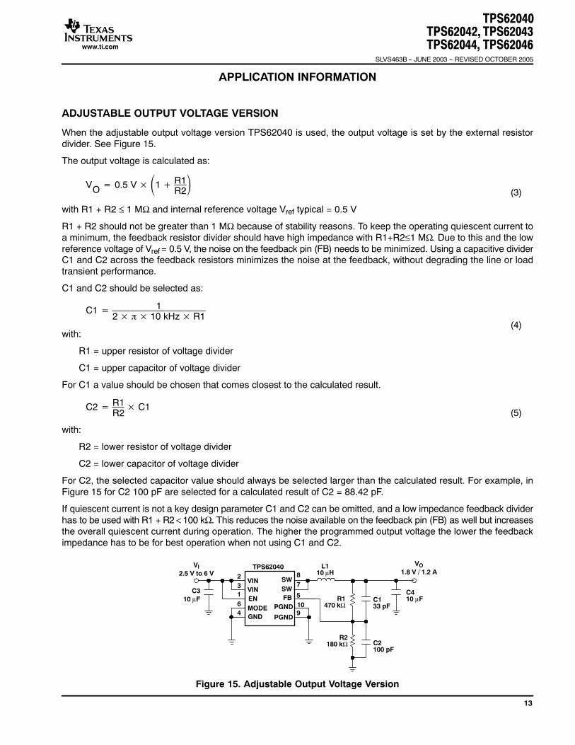
ADJUSTABLE OUTPUT VOLTAGE VERSION
When the adjustable output voltage version TPS62040 is used, the output voltage is set by the external resistordivider. See Figure 15.
The output voltage is calculated as:
VO 0.5 V 1 R1R2
with R1 + R2 ≤ 1 MΩ and internal reference voltage Vref typical = 0.5 V
R1 + R2 should not be greater than 1 MΩ because of stability reasons. To keep the operating quiescent current toa minimum, the feedback resistor divider should have high impedance with R1+R2≤1 MΩ. Due to this and the lowreference voltage of Vref = 0.5 V, the noise on the feedback pin (FB) needs to be minimized. Using a capacitive dividerC1 and C2 across the feedback resistors minimizes the noise at the feedback, without degrading the line or loadtransient performance.
C1 and C2 should be selected as:
C1 12 10 kHz R1
with:
R1 = upper resistor of voltage divider
C1 = upper capacitor of voltage divider
For C1 a value should be chosen that comes closest to the calculated result.
C2 R1R2
C1
with:
R2 = lower resistor of voltage divider
C2 = lower capacitor of voltage divider
For C2, the selected capacitor value should always be selected larger than the calculated result. For example, inFigure 15 for C2 100 pF are selected for a calculated result of C2 = 88.42 pF.
If quiescent current is not a key design parameter C1 and C2 can be omitted, and a low impedance feedback dividerhas to be used with R1 + R2 < 100 kΩ. This reduces the noise available on the feedback pin (FB) as well but increasesthe overall quiescent current during operation. The higher the programmed output voltage the lower the feedbackimpedance has to be for best operation when not using C1 and C2.
VINVINENMODE
SW
FBPGND
PGND
SW
GND
231
4 9105
78
6
TPS62040
C310 µF
VI2.5 V to 6 V
L110 µH
C410 µF
VO1.8 V / 1.2 A
R1470 kΩ
R2180 kΩ
C133 pF
C2100 pF
Figure 15. Adjustable Output Voltage Version
(3)
(4)
(5)
TPS62040TPS62042, TPS62043TPS62044, TPS62046SLVS463B − JUNE 2003 − REVISED OCTOBER 2005
www.ti.com
14
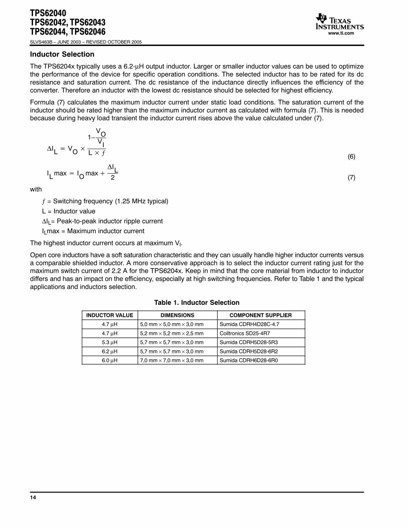
Inductor Selection
The TPS6204x typically uses a 6.2-µH output inductor. Larger or smaller inductor values can be used to optimizethe performance of the device for specific operation conditions. The selected inductor has to be rated for its dcresistance and saturation current. The dc resistance of the inductance directly influences the efficiency of theconverter. Therefore an inductor with the lowest dc resistance should be selected for highest efficiency.
Formula (7) calculates the maximum inductor current under static load conditions. The saturation current of theinductor should be rated higher than the maximum inductor current as calculated with formula (7). This is neededbecause during heavy load transient the inductor current rises above the value calculated under (7).
IL VO
1–VOVI
L ƒ
IL max IO maxIL2
with
ƒ = Switching frequency (1.25 MHz typical)
L = Inductor value
∆IL= Peak-to-peak inductor ripple current
ILmax = Maximum inductor current
The highest inductor current occurs at maximum VI.
Open core inductors have a soft saturation characteristic and they can usually handle higher inductor currents versusa comparable shielded inductor. A more conservative approach is to select the inductor current rating just for themaximum switch current of 2.2 A for the TPS6204x. Keep in mind that the core material from inductor to inductordiffers and has an impact on the efficiency, especially at high switching frequencies. Refer to Table 1 and the typicalapplications and inductors selection.
Table 1. Inductor Selection
INDUCTOR VALUE DIMENSIONS COMPONENT SUPPLIER
4.7 µH 5,0 mm × 5,0 mm × 3,0 mm Sumida CDRH4D28C-4.7
4.7 µH 5,2 mm × 5,2 mm × 2,5 mm Coiltronics SD25-4R7
5.3 µH 5,7 mm × 5,7 mm × 3,0 mm Sumida CDRH5D28-5R3
6.2 µH 5,7 mm × 5,7 mm × 3,0 mm Sumida CDRH5D28-6R2
6.0 µH 7,0 mm × 7,0 mm × 3,0 mm Sumida CDRH6D28-6R0
(6)
(7)

TPS62040TPS62042, TPS62043TPS62044, TPS62046
SLVS463B − JUNE 2003 − REVISED OCTOBER 2005
www.ti.com
15
Output Capacitor Selection
The advanced fast response voltage mode control scheme of the TPS6204x allows the use of small ceramiccapacitors with a typical value of 22 µF without having large output voltage under and overshoots during heavy loadtransients. Ceramic capacitors having low ESR values have the lowest output voltage ripple and are recommended.If required, tantalum capacitors may also be used. Refer to Table 2 for component selection.
If ceramic output capacitor are used, the capacitor RMS ripple current rating always meets the applicationrequirements. Just for completeness the RMS ripple current is calculated as:
IRMSCout VO
1–VOVI
L ƒ 12 3
At nominal load current the device operates in PWM mode and the overall output voltage ripple is the sum of thevoltage spike caused by the output capacitor ESR plus the voltage ripple caused by charging and discharging theoutput capacitor:
VO VO
1–VOVI
L ƒ 18 CO ƒ ESR
Where the highest output voltage ripple occurs at the highest input voltage, VI.
At light load currents, the device operates in power save mode and the output voltage ripple is independent of theoutput capacitor value. The output voltage ripple is set by the internal comparator thresholds. The typical outputvoltage ripple is 1% of the nominal output voltage.
Input Capacitor Selection
Because of the nature of the buck converter having a pulsating input current, a low ESR input capacitor is requiredfor best input voltage filtering and minimizing the interference with other circuits caused by high input voltage spikes.The input capacitor should have a minimum value of 22 µF. The input capacitor can be increased without any limitfor better input voltage filtering.
Table 2. Input and Output Capacitor Selection
CAPACITORVALUE
CASE SIZE COMPONENT SUPPLIER COMMENTS
22 µF 1206 Taiyo Yuden JMK316BJ226ML Ceramic
22 µF 1210 Taiyo Yuden JMK325BJ226MM Ceramic
(8)
(9)

TPS62040TPS62042, TPS62043TPS62044, TPS62046SLVS463B − JUNE 2003 − REVISED OCTOBER 2005
www.ti.com
16
Layout Considerations
For all switching power supplies, the layout is an important step in the design especially at high peak currents andswitching frequencies. If the layout is not carefully done, the regulator might show stability problems as well as EMIproblems. Therefore, use wide and short traces for the main current paths as indicated in bold in Figure 16. Thesetraces should be routed first. The input capacitor should be placed as close as possible to the IC pins as well as theinductor and output capacitor. The feedback resistor network should be routed away from the inductor and switchnode to minimize noise and magnetic interference. To further minimize noise from coupling into the feedback networkand feedback pin, the ground plane or ground traces should be used for shielding. A common ground plane or a starground as shown below should be used. This becomes very important especially at high switching frequencies of1.25 MHz.
VINVINENMODE
SW
FBPGND
PGND
SW
GND
231
4 9
1057
8
6
TPS6204x
C322 µF
VI
L110 µH
C222 µF
VO
The Switch Node Must BeKept as Small as Possible
Figure 16. Layout Diagram
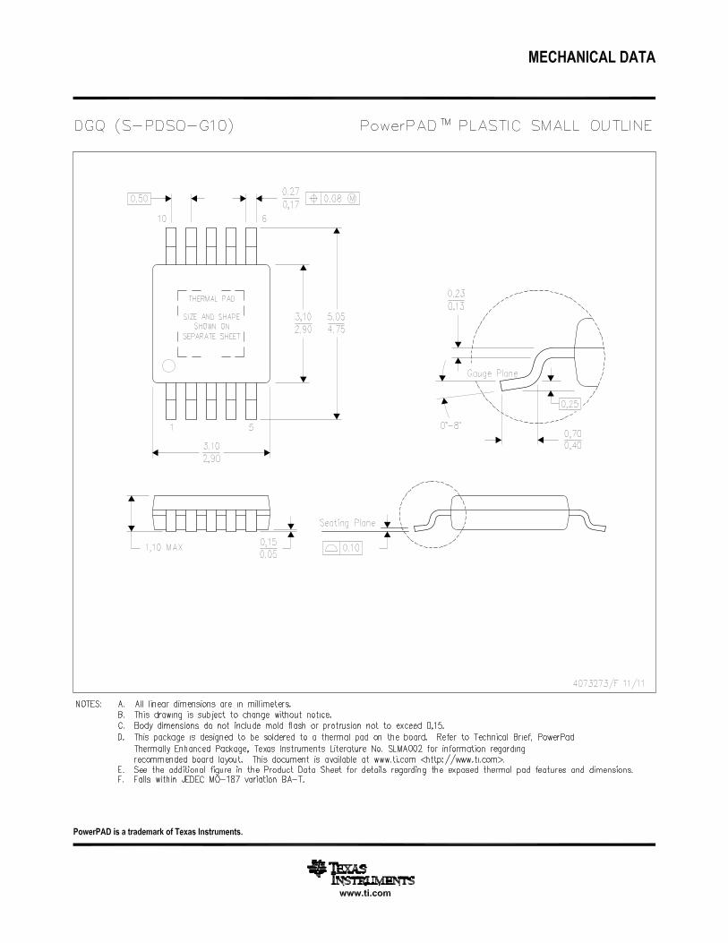
THERMAL INFORMATION
One of the most influential components on the thermal performance of a package is board design. In order to takefull advantage of the heat dissipating abilities of the PowerPAD packages, a board should be used that acts similarto a heat sink and allows for the use of the exposed (and solderable), deep downset pad. For further informationplease refer to Texas Instruments application note (SLMA002) PowerPAD Thermally Enhanced Package.
The PowerPAD of the 10-pin MSOP package has an area of 1,52 mm × 1,79 mm (± 0,05 mm) and must be solderedto the PCB to lower the thermal resistance. Thermal vias to the next layer further reduce the thermal resistance.

TPS62040TPS62042, TPS62043TPS62044, TPS62046
SLVS463B − JUNE 2003 − REVISED OCTOBER 2005
www.ti.com
17
TYPICAL APPLICATIONS
7VIN
VINEN
MODE
SW
FB
PGND
PGND
SW
GND
2
31
4 9
10
5
8
6
TPS62046VILi-lon
VO3.3 V / 1.2 A
C222 µF
C122 µF
L16.2 µH
Components:C1: Taiyo Yuden JMK316BJ226MLC2: Taiyo Yuden JMK316BJ226MLL1: Sumida CDRH5D28−6R2
Figure 17. Li-Ion to 3.3 V/1.2 A Conversion
VINVINENMODE
SW
FBPGND
PGND
SW
GND
231
4 91057
8
6
TPS62040
C322 µF
VI2.5 V to 6 V
L14.7 µH
C422 µF
VO1.8 V / 1.2 A
Components:C1: Taiyo Yuden JMK316BJ226MLC2: Taiyo Yuden JMK316BJ226MLL1: Sumida CDRH4D28C−4R7
R1470 kΩ
R2180 kΩ
C133 pF
C2100 pF
Figure 18. Li-Ion to 1.8 V/1.2 A Conversion Using the Adjustable Output Voltage Version

PACKAGE OPTION ADDENDUM
www.ti.com 15-Apr-2017
Addendum-Page 1
PACKAGING INFORMATION
Orderable Device Status(1)
Package Type PackageDrawing
Pins PackageQty
Eco Plan(2)
Lead/Ball Finish(6)
MSL Peak Temp(3)
Op Temp (°C) Device Marking(4/5)
Samples
HPA00355DRCR ACTIVE VSON DRC 10 3000 Green (RoHS& no Sb/Br)
CU NIPDAU Level-2-260C-1 YEAR -40 to 85 BBO
TPS62040DGQ ACTIVE MSOP-PowerPAD
DGQ 10 80 Green (RoHS& no Sb/Br)
CU NIPDAUAG Level-1-260C-UNLIM -40 to 85 BBI
TPS62040DGQG4 ACTIVE MSOP-PowerPAD
DGQ 10 80 Green (RoHS& no Sb/Br)
CU NIPDAUAG Level-1-260C-UNLIM -40 to 85 BBI
TPS62040DGQR ACTIVE MSOP-PowerPAD
DGQ 10 2500 Green (RoHS& no Sb/Br)
CU NIPDAUAG Level-1-260C-UNLIM -40 to 85 BBI
TPS62040DGQRG4 ACTIVE MSOP-PowerPAD
DGQ 10 2500 Green (RoHS& no Sb/Br)
CU NIPDAUAG Level-1-260C-UNLIM -40 to 85 BBI
TPS62040DRCR ACTIVE VSON DRC 10 3000 Green (RoHS& no Sb/Br)
CU NIPDAU Level-2-260C-1 YEAR -40 to 85 BBO
TPS62040DRCRG4 ACTIVE VSON DRC 10 3000 Green (RoHS& no Sb/Br)
CU NIPDAU Level-2-260C-1 YEAR -40 to 85 BBO
TPS62042DGQ ACTIVE MSOP-PowerPAD
DGQ 10 80 Green (RoHS& no Sb/Br)
CU NIPDAUAG Level-1-260C-UNLIM -40 to 85 BBL
TPS62042DGQG4 ACTIVE MSOP-PowerPAD
DGQ 10 80 Green (RoHS& no Sb/Br)
CU NIPDAUAG Level-1-260C-UNLIM -40 to 85 BBL
TPS62042DGQR ACTIVE MSOP-PowerPAD
DGQ 10 2500 Green (RoHS& no Sb/Br)
CU NIPDAUAG Level-1-260C-UNLIM -40 to 85 BBL
TPS62042DGQRG4 ACTIVE MSOP-PowerPAD
DGQ 10 2500 Green (RoHS& no Sb/Br)
CU NIPDAUAG Level-1-260C-UNLIM -40 to 85 BBL
TPS62042DRCR ACTIVE VSON DRC 10 3000 Green (RoHS& no Sb/Br)
CU NIPDAU Level-2-260C-1 YEAR -40 to 85 BBS
TPS62042DRCRG4 ACTIVE VSON DRC 10 3000 Green (RoHS& no Sb/Br)
CU NIPDAU Level-2-260C-1 YEAR -40 to 85 BBS
TPS62043DGQ ACTIVE MSOP-PowerPAD
DGQ 10 80 Green (RoHS& no Sb/Br)
CU NIPDAUAG Level-1-260C-UNLIM -40 to 85 BBM
TPS62043DGQR ACTIVE MSOP-PowerPAD
DGQ 10 2500 Green (RoHS& no Sb/Br)
CU NIPDAUAG Level-1-260C-UNLIM -40 to 85 BBM
TPS62043DRCR ACTIVE VSON DRC 10 3000 Green (RoHS& no Sb/Br)
CU NIPDAU Level-2-260C-1 YEAR -40 to 85 BBT
TPS62044DGQ ACTIVE MSOP-PowerPAD
DGQ 10 80 Green (RoHS& no Sb/Br)
CU NIPDAUAG Level-1-260C-UNLIM -40 to 85 BBN
PACKAGE OPTION ADDENDUM
www.ti.com 15-Apr-2017
Addendum-Page 2
Orderable Device Status(1)
Package Type PackageDrawing
Pins PackageQty
Eco Plan(2)
Lead/Ball Finish(6)
MSL Peak Temp(3)
Op Temp (°C) Device Marking(4/5)
Samples
TPS62044DGQG4 ACTIVE MSOP-PowerPAD
DGQ 10 80 Green (RoHS& no Sb/Br)
CU NIPDAUAG Level-1-260C-UNLIM -40 to 85 BBN
TPS62044DGQR ACTIVE MSOP-PowerPAD
DGQ 10 2500 Green (RoHS& no Sb/Br)
CU NIPDAUAG Level-1-260C-UNLIM -40 to 85 BBN
TPS62044DGQRG4 ACTIVE MSOP-PowerPAD
DGQ 10 2500 Green (RoHS& no Sb/Br)
CU NIPDAUAG Level-1-260C-UNLIM -40 to 85 BBN
TPS62044DRCR ACTIVE VSON DRC 10 3000 Green (RoHS& no Sb/Br)
CU NIPDAU Level-2-260C-1 YEAR -40 to 85 BBU
TPS62044DRCRG4 ACTIVE VSON DRC 10 3000 Green (RoHS& no Sb/Br)
CU NIPDAU Level-2-260C-1 YEAR -40 to 85 BBU
TPS62046DGQ ACTIVE MSOP-PowerPAD
DGQ 10 80 Green (RoHS& no Sb/Br)
CU NIPDAUAG Level-1-260C-UNLIM -40 to 85 BBQ
TPS62046DGQG4 ACTIVE MSOP-PowerPAD
DGQ 10 80 Green (RoHS& no Sb/Br)
CU NIPDAUAG Level-1-260C-UNLIM -40 to 85 BBQ
TPS62046DGQR ACTIVE MSOP-PowerPAD
DGQ 10 2500 Green (RoHS& no Sb/Br)
CU NIPDAUAG Level-1-260C-UNLIM -40 to 85 BBQ
TPS62046DGQRG4 ACTIVE MSOP-PowerPAD
DGQ 10 2500 Green (RoHS& no Sb/Br)
CU NIPDAUAG Level-1-260C-UNLIM -40 to 85 BBQ
TPS62046DRCR ACTIVE VSON DRC 10 3000 Green (RoHS& no Sb/Br)
CU NIPDAU Level-2-260C-1 YEAR -40 to 85 BBW
(1) The marketing status values are defined as follows:ACTIVE: Product device recommended for new designs.LIFEBUY: TI has announced that the device will be discontinued, and a lifetime-buy period is in effect.NRND: Not recommended for new designs. Device is in production to support existing customers, but TI does not recommend using this part in a new design.PREVIEW: Device has been announced but is not in production. Samples may or may not be available.OBSOLETE: TI has discontinued the production of the device.
(2) Eco Plan - The planned eco-friendly classification: Pb-Free (RoHS), Pb-Free (RoHS Exempt), or Green (RoHS & no Sb/Br) - please check http://www.ti.com/productcontent for the latest availabilityinformation and additional product content details.TBD: The Pb-Free/Green conversion plan has not been defined.Pb-Free (RoHS): TI's terms "Lead-Free" or "Pb-Free" mean semiconductor products that are compatible with the current RoHS requirements for all 6 substances, including the requirement thatlead not exceed 0.1% by weight in homogeneous materials. Where designed to be soldered at high temperatures, TI Pb-Free products are suitable for use in specified lead-free processes.Pb-Free (RoHS Exempt): This component has a RoHS exemption for either 1) lead-based flip-chip solder bumps used between the die and package, or 2) lead-based die adhesive used betweenthe die and leadframe. The component is otherwise considered Pb-Free (RoHS compatible) as defined above.Green (RoHS & no Sb/Br): TI defines "Green" to mean Pb-Free (RoHS compatible), and free of Bromine (Br) and Antimony (Sb) based flame retardants (Br or Sb do not exceed 0.1% by weightin homogeneous material)

PACKAGE OPTION ADDENDUM
www.ti.com 15-Apr-2017
Addendum-Page 3
(3) MSL, Peak Temp. - The Moisture Sensitivity Level rating according to the JEDEC industry standard classifications, and peak solder temperature.
(4) There may be additional marking, which relates to the logo, the lot trace code information, or the environmental category on the device.
(5) Multiple Device Markings will be inside parentheses. Only one Device Marking contained in parentheses and separated by a "~" will appear on a device. If a line is indented then it is a continuationof the previous line and the two combined represent the entire Device Marking for that device.
(6) Lead/Ball Finish - Orderable Devices may have multiple material finish options. Finish options are separated by a vertical ruled line. Lead/Ball Finish values may wrap to two lines if the finishvalue exceeds the maximum column width.
Important Information and Disclaimer:The information provided on this page represents TI's knowledge and belief as of the date that it is provided. TI bases its knowledge and belief on informationprovided by third parties, and makes no representation or warranty as to the accuracy of such information. Efforts are underway to better integrate information from third parties. TI has taken andcontinues to take reasonable steps to provide representative and accurate information but may not have conducted destructive testing or chemical analysis on incoming materials and chemicals.TI and TI suppliers consider certain information to be proprietary, and thus CAS numbers and other limited information may not be available for release.
In no event shall TI's liability arising out of such information exceed the total purchase price of the TI part(s) at issue in this document sold by TI to Customer on an annual basis.
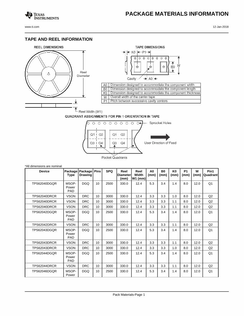
TAPE AND REEL INFORMATION
*All dimensions are nominal
Device PackageType
PackageDrawing
Pins SPQ ReelDiameter
(mm)
ReelWidth
W1 (mm)
A0(mm)
B0(mm)
K0(mm)
P1(mm)
W(mm)
Pin1Quadrant
TPS62040DGQR MSOP-Power PAD
DGQ 10 2500 330.0 12.4 5.3 3.4 1.4 8.0 12.0 Q1
TPS62040DRCR VSON DRC 10 3000 330.0 12.4 3.3 3.3 1.0 8.0 12.0 Q2
TPS62040DRCR VSON DRC 10 3000 330.0 12.4 3.3 3.3 1.1 8.0 12.0 Q2
TPS62040DRCR VSON DRC 10 3000 330.0 12.4 3.3 3.3 1.1 8.0 12.0 Q2
TPS62042DGQR MSOP-Power PAD
DGQ 10 2500 330.0 12.4 5.3 3.4 1.4 8.0 12.0 Q1
TPS62042DRCR VSON DRC 10 3000 330.0 12.4 3.3 3.3 1.1 8.0 12.0 Q2
TPS62043DGQR MSOP-Power PAD
DGQ 10 2500 330.0 12.4 5.3 3.4 1.4 8.0 12.0 Q1
TPS62043DRCR VSON DRC 10 3000 330.0 12.4 3.3 3.3 1.1 8.0 12.0 Q2
TPS62043DRCR VSON DRC 10 3000 330.0 12.4 3.3 3.3 1.0 8.0 12.0 Q2
TPS62044DGQR MSOP-Power PAD
DGQ 10 2500 330.0 12.4 5.3 3.4 1.4 8.0 12.0 Q1
TPS62044DRCR VSON DRC 10 3000 330.0 12.4 3.3 3.3 1.1 8.0 12.0 Q2
TPS62046DGQR MSOP-Power
DGQ 10 2500 330.0 12.4 5.3 3.4 1.4 8.0 12.0 Q1
PACKAGE MATERIALS INFORMATION
www.ti.com 12-Jan-2018
Pack Materials-Page 1

Device PackageType
PackageDrawing
Pins SPQ ReelDiameter
(mm)
ReelWidth
W1 (mm)
A0(mm)
B0(mm)
K0(mm)
P1(mm)
W(mm)
Pin1Quadrant
PAD
TPS62046DRCR VSON DRC 10 3000 330.0 12.4 3.3 3.3 1.1 8.0 12.0 Q2
TPS62046DRCR VSON DRC 10 3000 330.0 12.4 3.3 3.3 1.0 8.0 12.0 Q2
*All dimensions are nominal
Device Package Type Package Drawing Pins SPQ Length (mm) Width (mm) Height (mm)
TPS62040DGQR MSOP-PowerPAD DGQ 10 2500 364.0 364.0 27.0
TPS62040DRCR VSON DRC 10 3000 370.0 355.0 55.0
TPS62040DRCR VSON DRC 10 3000 367.0 367.0 35.0
TPS62040DRCR VSON DRC 10 3000 367.0 367.0 35.0
TPS62042DGQR MSOP-PowerPAD DGQ 10 2500 364.0 364.0 27.0
TPS62042DRCR VSON DRC 10 3000 367.0 367.0 35.0
TPS62043DGQR MSOP-PowerPAD DGQ 10 2500 364.0 364.0 27.0
TPS62043DRCR VSON DRC 10 3000 367.0 367.0 35.0
TPS62043DRCR VSON DRC 10 3000 370.0 355.0 55.0
TPS62044DGQR MSOP-PowerPAD DGQ 10 2500 364.0 364.0 27.0
TPS62044DRCR VSON DRC 10 3000 367.0 367.0 35.0
TPS62046DGQR MSOP-PowerPAD DGQ 10 2500 364.0 364.0 27.0
TPS62046DRCR VSON DRC 10 3000 367.0 367.0 35.0
TPS62046DRCR VSON DRC 10 3000 370.0 355.0 55.0
PACKAGE MATERIALS INFORMATION
www.ti.com 12-Jan-2018
Pack Materials-Page 2


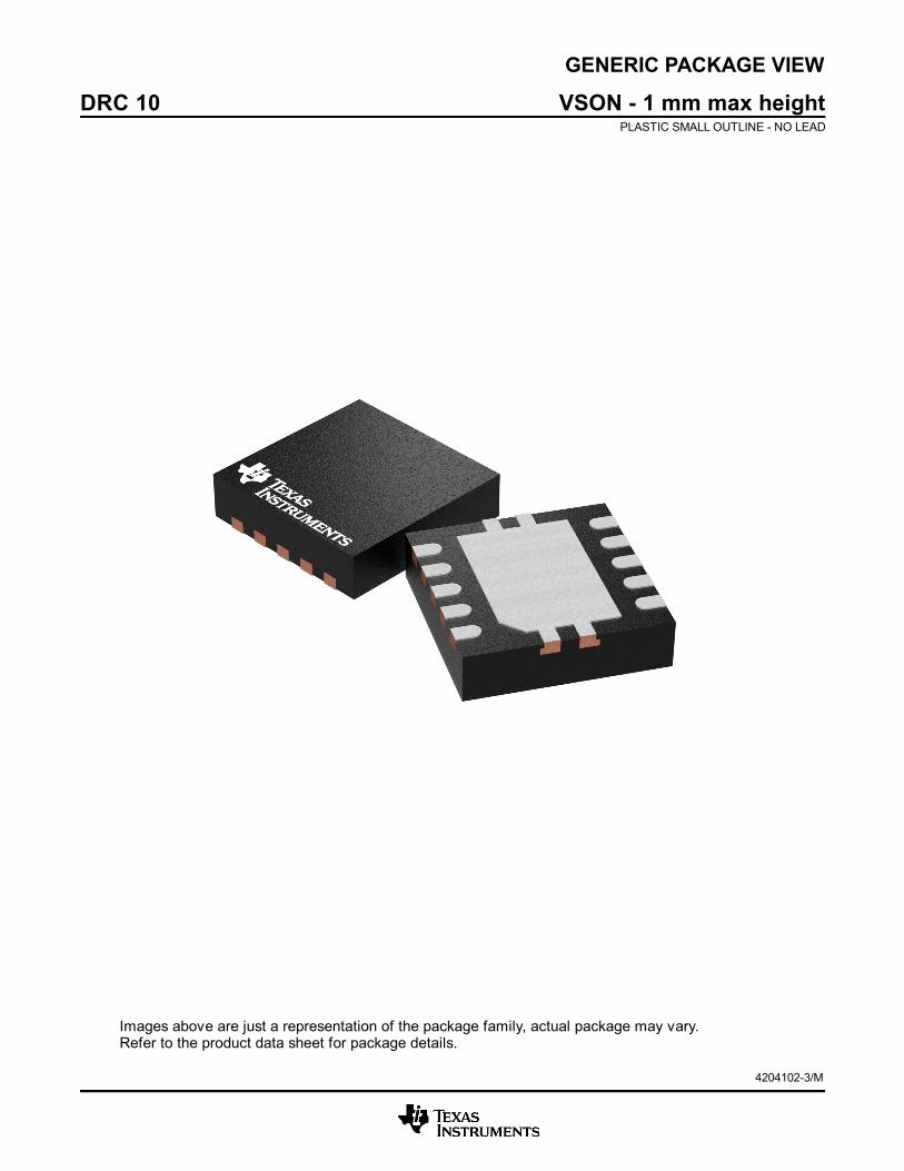
GENERIC PACKAGE VIEW
Images above are just a representation of the package family, actual package may vary.Refer to the product data sheet for package details.
DRC 10 VSON - 1 mm max heightPLASTIC SMALL OUTLINE - NO LEAD
4204102-3/M

www.ti.com
PACKAGE OUTLINE
C
10X 0.300.18
2.4 0.1
2X2
1.65 0.1
8X 0.5
1.00.8
10X 0.50.3
0.050.00
A 3.12.9
B
3.12.9
(0.2) TYP4X (0.25)
2X (0.5)
VSON - 1 mm max heightDRC0010JPLASTIC SMALL OUTLINE - NO LEAD
4218878/B 07/2018
PIN 1 INDEX AREA
SEATING PLANE
0.08 C
1
5 6
10
(OPTIONAL)PIN 1 ID 0.1 C A B
0.05 C
THERMAL PADEXPOSED
SYMM
SYMM11
NOTES: 1. All linear dimensions are in millimeters. Any dimensions in parenthesis are for reference only. Dimensioning and tolerancing per ASME Y14.5M. 2. This drawing is subject to change without notice. 3. The package thermal pad must be soldered to the printed circuit board for optimal thermal and mechanical performance.
SCALE 4.000

www.ti.com
EXAMPLE BOARD LAYOUT
0.07 MINALL AROUND0.07 MAX
ALL AROUND
10X (0.24)
(2.4)
(2.8)
8X (0.5)
(1.65)
( 0.2) VIATYP
(0.575)
(0.95)
10X (0.6)
(R0.05) TYP
(3.4)
(0.25)
(0.5)
VSON - 1 mm max heightDRC0010JPLASTIC SMALL OUTLINE - NO LEAD
4218878/B 07/2018
SYMM
1
5 6
10
LAND PATTERN EXAMPLEEXPOSED METAL SHOWN
SCALE:20X
11SYMM
NOTES: (continued) 4. This package is designed to be soldered to a thermal pad on the board. For more information, see Texas Instruments literature number SLUA271 (www.ti.com/lit/slua271).5. Vias are optional depending on application, refer to device data sheet. If any vias are implemented, refer to their locations shown on this view. It is recommended that vias under paste be filled, plugged or tented.
SOLDER MASKOPENINGSOLDER MASK
METAL UNDER
SOLDER MASKDEFINED
EXPOSED METAL
METALSOLDER MASKOPENING
SOLDER MASK DETAILS
NON SOLDER MASKDEFINED
(PREFERRED)
EXPOSED METAL

www.ti.com
EXAMPLE STENCIL DESIGN
(R0.05) TYP
10X (0.24)
10X (0.6)
2X (1.5)
2X(1.06)
(2.8)
(0.63)
8X (0.5)
(0.5)
4X (0.34)
4X (0.25)
(1.53)
VSON - 1 mm max heightDRC0010JPLASTIC SMALL OUTLINE - NO LEAD
4218878/B 07/2018
NOTES: (continued) 6. Laser cutting apertures with trapezoidal walls and rounded corners may offer better paste release. IPC-7525 may have alternate design recommendations.
SOLDER PASTE EXAMPLEBASED ON 0.125 mm THICK STENCIL
EXPOSED PAD 11:
80% PRINTED SOLDER COVERAGE BY AREASCALE:25X
SYMM
1
56
10
EXPOSED METALTYP11
SYMM
IMPORTANT NOTICE
Texas Instruments Incorporated (TI) reserves the right to make corrections, enhancements, improvements and other changes to itssemiconductor products and services per JESD46, latest issue, and to discontinue any product or service per JESD48, latest issue. Buyersshould obtain the latest relevant information before placing orders and should verify that such information is current and complete.TI’s published terms of sale for semiconductor products (http://www.ti.com/sc/docs/stdterms.htm) apply to the sale of packaged integratedcircuit products that TI has qualified and released to market. Additional terms may apply to the use or sale of other types of TI products andservices.Reproduction of significant portions of TI information in TI data sheets is permissible only if reproduction is without alteration and isaccompanied by all associated warranties, conditions, limitations, and notices. TI is not responsible or liable for such reproduceddocumentation. Information of third parties may be subject to additional restrictions. Resale of TI products or services with statementsdifferent from or beyond the parameters stated by TI for that product or service voids all express and any implied warranties for theassociated TI product or service and is an unfair and deceptive business practice. TI is not responsible or liable for any such statements.Buyers and others who are developing systems that incorporate TI products (collectively, “Designers”) understand and agree that Designersremain responsible for using their independent analysis, evaluation and judgment in designing their applications and that Designers havefull and exclusive responsibility to assure the safety of Designers' applications and compliance of their applications (and of all TI productsused in or for Designers’ applications) with all applicable regulations, laws and other applicable requirements. Designer represents that, withrespect to their applications, Designer has all the necessary expertise to create and implement safeguards that (1) anticipate dangerousconsequences of failures, (2) monitor failures and their consequences, and (3) lessen the likelihood of failures that might cause harm andtake appropriate actions. Designer agrees that prior to using or distributing any applications that include TI products, Designer willthoroughly test such applications and the functionality of such TI products as used in such applications.TI’s provision of technical, application or other design advice, quality characterization, reliability data or other services or information,including, but not limited to, reference designs and materials relating to evaluation modules, (collectively, “TI Resources”) are intended toassist designers who are developing applications that incorporate TI products; by downloading, accessing or using TI Resources in anyway, Designer (individually or, if Designer is acting on behalf of a company, Designer’s company) agrees to use any particular TI Resourcesolely for this purpose and subject to the terms of this Notice.TI’s provision of TI Resources does not expand or otherwise alter TI’s applicable published warranties or warranty disclaimers for TIproducts, and no additional obligations or liabilities arise from TI providing such TI Resources. TI reserves the right to make corrections,enhancements, improvements and other changes to its TI Resources. TI has not conducted any testing other than that specificallydescribed in the published documentation for a particular TI Resource.Designer is authorized to use, copy and modify any individual TI Resource only in connection with the development of applications thatinclude the TI product(s) identified in such TI Resource. NO OTHER LICENSE, EXPRESS OR IMPLIED, BY ESTOPPEL OR OTHERWISETO ANY OTHER TI INTELLECTUAL PROPERTY RIGHT, AND NO LICENSE TO ANY TECHNOLOGY OR INTELLECTUAL PROPERTYRIGHT OF TI OR ANY THIRD PARTY IS GRANTED HEREIN, including but not limited to any patent right, copyright, mask work right, orother intellectual property right relating to any combination, machine, or process in which TI products or services are used. Informationregarding or referencing third-party products or services does not constitute a license to use such products or services, or a warranty orendorsement thereof. Use of TI Resources may require a license from a third party under the patents or other intellectual property of thethird party, or a license from TI under the patents or other intellectual property of TI.TI RESOURCES ARE PROVIDED “AS IS” AND WITH ALL FAULTS. TI DISCLAIMS ALL OTHER WARRANTIES ORREPRESENTATIONS, EXPRESS OR IMPLIED, REGARDING RESOURCES OR USE THEREOF, INCLUDING BUT NOT LIMITED TOACCURACY OR COMPLETENESS, TITLE, ANY EPIDEMIC FAILURE WARRANTY AND ANY IMPLIED WARRANTIES OFMERCHANTABILITY, FITNESS FOR A PARTICULAR PURPOSE, AND NON-INFRINGEMENT OF ANY THIRD PARTY INTELLECTUALPROPERTY RIGHTS. TI SHALL NOT BE LIABLE FOR AND SHALL NOT DEFEND OR INDEMNIFY DESIGNER AGAINST ANY CLAIM,INCLUDING BUT NOT LIMITED TO ANY INFRINGEMENT CLAIM THAT RELATES TO OR IS BASED ON ANY COMBINATION OFPRODUCTS EVEN IF DESCRIBED IN TI RESOURCES OR OTHERWISE. IN NO EVENT SHALL TI BE LIABLE FOR ANY ACTUAL,DIRECT, SPECIAL, COLLATERAL, INDIRECT, PUNITIVE, INCIDENTAL, CONSEQUENTIAL OR EXEMPLARY DAMAGES INCONNECTION WITH OR ARISING OUT OF TI RESOURCES OR USE THEREOF, AND REGARDLESS OF WHETHER TI HAS BEENADVISED OF THE POSSIBILITY OF SUCH DAMAGES.Unless TI has explicitly designated an individual product as meeting the requirements of a particular industry standard (e.g., ISO/TS 16949and ISO 26262), TI is not responsible for any failure to meet such industry standard requirements.Where TI specifically promotes products as facilitating functional safety or as compliant with industry functional safety standards, suchproducts are intended to help enable customers to design and create their own applications that meet applicable functional safety standardsand requirements. Using products in an application does not by itself establish any safety features in the application. Designers mustensure compliance with safety-related requirements and standards applicable to their applications. Designer may not use any TI products inlife-critical medical equipment unless authorized officers of the parties have executed a special contract specifically governing such use.Life-critical medical equipment is medical equipment where failure of such equipment would cause serious bodily injury or death (e.g., lifesupport, pacemakers, defibrillators, heart pumps, neurostimulators, and implantables). Such equipment includes, without limitation, allmedical devices identified by the U.S. Food and Drug Administration as Class III devices and equivalent classifications outside the U.S.TI may expressly designate certain products as completing a particular qualification (e.g., Q100, Military Grade, or Enhanced Product).Designers agree that it has the necessary expertise to select the product with the appropriate qualification designation for their applicationsand that proper product selection is at Designers’ own risk. Designers are solely responsible for compliance with all legal and regulatoryrequirements in connection with such selection.Designer will fully indemnify TI and its representatives against any damages, costs, losses, and/or liabilities arising out of Designer’s non-compliance with the terms and provisions of this Notice.
Mailing Address: Texas Instruments, Post Office Box 655303, Dallas, Texas 75265Copyright © 2018, Texas Instruments Incorporated