10gbps dual-channel multi-rate serial link aggregator … · required for a certain data throughput...
TRANSCRIPT

2.5GBPS
ASSP 1 ASSP 3
2.5GBPS
2.5GBPS
2.5GBPS
2.5GBPS
2.5GBPS
2.5GBPS
2.5GBPS
2.5GBPS
2.5GBPS
2.5GBPS
2.5GBPS
2.5GBPS
2.5GBPS
2.5GBPS
2.5GBPS
ASSP 2 ASSP 4
BackplaneOptical
ASSP 1 ASSP 3
10GBPS10GBPS
TLK10022 TLK1002210GBPS10GBPS
ASSP 2 ASSP 4
Backplane/Optical
TLK10022
www.ti.com SLLSEE7 –NOVEMBER 2013
10Gbps DUAL-CHANNEL MULTI-RATE SERIAL LINK AGGREGATORCheck for Samples: TLK10022
1 INTRODUCTION1.1 Features1
• Automatic Digital Multiplexing/De-Multiplexing • Core Supply 1V; I/O: 1.5V/1.8Vof 4, 3, or 2 Independent Lower-Speed Gigabit • Programmable High SpeedSerial Lines into a Single Higher-Speed Gigabit Scrambling/Descrambling Functions ImproveSerial Line Serial Link Transition Density and Reduce
• 4 x (0.25 to 2.5 Gbps) to 1 x (1 to 10 Gbps) Spectral PeaksMultiplexing • Superior Signal Integrity Performance
• 3 x (0.5 to 3.33 Gbps) to 1x (1.5 to 10 Gbps) • Low Power Operation: < 800mW per Channel• 2 x (0.5 to 5 Gbps) to 1 x (1 to 10 Gbps) (typ)• 1 x (0.5 to 2.5 Gbps) to 1 x (0.5 to 2.5 Gbps) • Flexible Clocking• Programmable Per Channel Lane Switching • Multi Drive Capability (SFP+, backplane, cable)• Wide Data Rate Range for Multiple Application • Support for Programmable Lane Marker
Support Character• Transmit De-Emphasis and Adaptive Receiver • Support for Programmable HS/LS 10-Bit
Equalization on Both Low Speed and High Alignment CharacterSpeed Sides • Wide Range of Built-in Test Patterns
• 8B/10B ENDEC Coding Support • 144-pin, 13mmx13mm FCBGA Package• Raw (unencoded) Data Support1.2 Applications• Gigabit Serial Link Aggregation • Machine Vision• Communications System Backplanes • Video/Image Data Processing
1
Please be aware that an important notice concerning availability, standard warranty, and use in critical applications ofTexas Instruments semiconductor products and disclaimers thereto appears at the end of this data sheet.
PRODUCTION DATA information is current as of publication date. Products conform to Copyright © 2013, Texas Instruments Incorporatedspecifications per the terms of the Texas Instruments standard warranty. Productionprocessing does not necessarily include testing of all parameters.

TLK10022
SLLSEE7 –NOVEMBER 2013 www.ti.com
1.3 DescriptionThe TLK10022 is a dual-channel multi-rate link aggregator intended for use in high-speed bi-directionalpoint-to-point data transmission systems. The device allows for a reduction in the number of physical linksrequired for a certain data throughput by multiplexing multiple lower-rate serial links into higher-rate seriallinks.
Each channel of the TLK10022 has a low-speed interface which can accommodate one, two, three, or fourbidirectional serial links running at rates from 250 Mbps to 5 Gbps (maximum of 10 Gbps total throughput).The device’s high speed interfaces (one per channel, bidirectional) can operate at rates from 1 Gbps to 10Gbps. When a channel is configured for a certain multiplexing ratio (1-to-1, 2-to-1, 3-to-1, or 4-to-1), thehigh speed side will operate at a fixed multiple of the low speed rate (e.g., four times faster for 4-to-1mode) regardless of the number of lanes connected. Filler data will be placed on any unused lanes inorder to keep the interleaved lane ordering constant. This allows for low speed lanes to be hot swappedduring normal operation without requiring a change in configuration.
The device has multiple interleaving/de-interleaving schemes that may be used depending on the datatype. These schemes allow for the low speed lane ordering to be recovered after the lanes are transmittedover a single high-speed link. There is also a programmable scrambling/de-scrambling function availableto help ensure that the high-speed data has suitable properties for transmission (i.e., sufficient transitiondensity for clock recovery and DC balance over time) even for non-ideal input data.
A 1:1 mode is also supported for data rates ranging from 0.5 Gbps to 2.5 Gbps, whereby both low speedand high speed are rate matched. The TX and RX datapaths are also independent, so the TX and RX canoperates in different modes (this excludes 3:1 mode which requires both the TX and RX path to run in thesame mode). This independence is restricted to using the same low speed line rate. For example, the TXcan operate at 4 x 2.5 Gbps while RX operates at 1 x 2.5 Gbps.
The individual Low Speed lanes may also operate at independent rates in byte interleave mode, providedthey are operating at integer multiples. The High Speed line rate must be configured based on the fastestLow Speed line rate.
The TLK10022 has the ability to perform lane alignment on 2, 3, or 4 lanes with up to four bytes of lanede-skew.
Both the low speed and high speed side interfaces (transmitters and receivers) use CML signaling withintegrated termination resistors and feature programmable transmitter de-emphasis levels and adaptivereceive equalization to help compensate for media impairments at higher frequencies. The device’s serialtransceivers used are capable of interfacing to optical modules as well as higher-loss connections such asPCB backplanes and controlled-impedance copper cabling.
To aid in system synchronization, the TLK10022 is capable of extracting clocking information from theserial input data streams and outputting a recovered clock signal. This recovered clock can be input to ajitter cleaner in order to provide a synchronized system clock. The device also has two reference clockinput ports and a flexible internal PLL, allowing for various serial rates to be supported with a singlereference clock input frequency.
The device has various built-in self-test features to aid with system validation and debugging. Amongthese are pattern generation and verification on all serial lanes as well as internal data loopback paths.
||
2 INTRODUCTION Copyright © 2013, Texas Instruments IncorporatedSubmit Documentation FeedbackProduct Folder Links: TLK10022

TLK10022 RX
D
E
M
U
X
FIFOSe
rde
s
1:1
0
8b/10b
M
U
X
Se
rde
s
1:2
0
SKEW
8b/10b
DSCR
M
U
X
M
U
X
M
U
X
Ch_sync
JOG
Se
rde
s
1:1
0
8b/10b
M
U
X
Se
rde
s
1:1
0
8b/10b
M
U
X
Se
rde
s
1:1
0
8b/10b
M
U
X
FIFO
FIFO
FIFO
Marker
Replace
Lane
Ordering
SKEW
SKEW
SKEW
TLK10022 TX
M
U
X
Se
rd
es
1:1
0 CH
SYNC
8b/10b
SCR
8b/10b
FIFO
M
U
X
M
U
X
M
U
X
M
U
X
Se
rd
es
1:2
0
Se
rd
es
1:1
0 CH
SYNC8b/10b
FIFO
M
U
X
Se
rd
es
1:1
0 CH
SYNC8b/10b
FIFO
M
U
X
Se
rd
es
1:1
0 CH
SYNC8b/10b
FIFO
M
U
X
Lane 0
Mark
TLK10022
www.ti.com SLLSEE7 –NOVEMBER 2013
2 BLOCK DIAGRAM
A simplified block diagram of the TLK10022 device is shown in Figure 2-1 for Channel A which is identicalto Channel B. This low-power transceiver consists of two serializer/deserializer (SERDES) blocks, one onthe low speed side and the other on the high speed side. The core logic blocks that lie between the lowspeed and high speed SerDes blocks carry out all the logic functions such as byte alignment,encoding/decoding, lane marking, and scrambling.
The TLK10022 provides a management data input/output (MDIO) interface as well as a JTAG interface fordevice configuration, control, and monitoring. Detailed descriptions of the TLK10022 pin functions areprovided in Table 2-1.
spacing
Figure 2-1. A Simplified One Channel Block Diagram of the TLK10022
Copyright © 2013, Texas Instruments Incorporated BLOCK DIAGRAM 3Submit Documentation FeedbackProduct Folder Links: TLK10022

1 2 3 4 5 6 7 8 9 10 11 12
A INA1P VSS INA0N INA0P VSS OUTA0P OUTA0N PDTRXA_N CLKOUTBP CLKOUTBN VSS HSRXAN
B INA1N INA2P VSS VSS OUTA1P OUTA1N VSS TMS PRBSEN RXCTRL_0 VSS HSRXAP
C VSS INA2N VDDRA_LS OUTA2P OUTA2N VSS VDDO0 TDI CLKOUTAP CLKOUTAN AMUXA VSS
D INA3P VDDA_LS VSS AMUXB VSS TDO VPP TCK GPO0 VSS VSS HSTXAP
E INA3N VSS OUTA3N VSS TRST_N VDDD DVDD VDDD LOSA PRTAD0 VDDRA_HS HSTXAN
F VSS VDDA_LS OUTA3P VDDT_LS VSS VDDD DVDD VSS VDDT_HS VSS VDDA_HS VSS
G VSS VDDA_LS VSS VDDT_LS VSS DVDD VSS DVDD PRTAD1 VDDA_HS VSS HSRXBN
H INB0P VSS OUTB0N VSS RESET_N VDDD DVDD VDDD GPO1 GPI1 VSS HSRXBP
J INB0N VDDA_LS OUTB0P PDTRXB_N VSS PRTAD3 MDIO MDC PRBS_PASS GPI0 VDDRB_HS VSS
K VSS INB1P VDDRB_LS OUTB1N OUTB1P VSS VDDO1 LOSB REFCLK1P REFCLK1N VSS HSTXBP
L INB2P INB1N VSS VSS OUTB2N OUTB2P VSS RXCTRL_1 PRTAD2 TESTEN VSS HSTXBN
M INB2N VSS INB3P INB3N VSS OUTB3N OUTB3P PRTAD4 REFCLK_SEL REFCLK0P REFCLK0N VSS
TLK10022
SLLSEE7 –NOVEMBER 2013 www.ti.com
2.1 PackageA 13-mm x 13-mm, 144-pin PBGA package with a ball pitch of 1 mm is used. The device pin-out is asshown in Figure 2-2 and is described in detail in Table 2-1 and Table 2-2.
Figure 2-2. The Pin-Out of the TLK10022
4 BLOCK DIAGRAM Copyright © 2013, Texas Instruments IncorporatedSubmit Documentation FeedbackProduct Folder Links: TLK10022

TLK10022
www.ti.com SLLSEE7 –NOVEMBER 2013
2.2 Terminal FunctionsThe details of the terminal functions of the TLK10022 device are provided in Table 2-1 and Table 2-2.
Table 2-1. Pin Description - Signal PinsTERMINAL DIRECTION
TYPE DESCRIPTIONSIGNAL BGA SUPPLY
CHANNEL A
Output High Speed Transmit Channel A Output. HSTXAP and HSTXAN comprise the high speed side transmitHSTXAP D12 CML direction Channel A differential serial output signal. During device reset (RESET_N asserted low) these pins areHSTXAN E12 VDDA_HS driven differential zero. These CML outputs must be AC coupled.
InputHSRXAP B12 High Speed Receive Channel A Input. HSRXAP and HSRXAN comprise the high speed side receive directionCMLHSRXAN A12 Channel A differential serial input signal. These CML input signals must be AC coupled.VDDA_HS
D1/E1 Input Low Speed Channel A Inputs. INAP and INAN comprise the low speed side transmit direction Channel AB2/C2INA[3:0]P/N CML differential input signals. Only INA[0] is used in 1:1 mode, and only INA[1:0] are used in 2:1 mode, and onlyA1/B1 VDDA_LS INA[2:0] are used in 3:1 mode. These signals must be AC coupled.A4/A3
F3/E3 Low Speed Channel A Outputs. OUTAP and OUTAN comprise the low speed side receive direction ChannelOutputC4/C5 A differential output signals. During device reset (RESET_N asserted low) these pins are driven differential zero.OUTA[3:0]P/N CMLB5/B6 Only OUTA[0] is used in 1:1 mode, only OUTA[1:0] are used in 2:1 mode, and only OUTA[2:0] are used in 3:1VDDA_LSA6/A7 mode. These signals must be AC coupled.
Channel A Receive Loss Of Signal (LOS) Indicator.LOSA=0: Signal detected.LOSA=1: Loss of signal.Loss of signal detection is based on the input signal level. When HSRXAP/N has a differential input signal swing
Output of ≤75 mVpp, LOSA will be asserted (if enabled). If the input signal is greater than 150 mVp-p, LOS will beLVCMOS deasserted. Outside of these ranges, the LOS indication is undefined.
LOSA E9 1.5V/1.8VOther functions can be observed on LOSA real-time, configured via MDIOVDDO0
40Ω Driver During device reset (RESET_N asserted low) this pin is driven low. During pin based power down (PDTRXA_Nasserted low), this pin is floating. During register based power down, this pin is floating.
It is highly recommended that LOSA be brought to an easily accessible point on the application board (header)in the event that debug is required.
Input Channel A Bit Interleave Lane Rotation Jog.LVCMOSRXCTRL_0 B10 A toggle of this pin, either from high to low or from low to high, causes a lane rotation of the HSRXAP/N source1.5V/1.8V data.VDDO0
OutputLVCMOS Channel A General Purpose Output.GPO0 D9 1.5V/1.8V This pin should be left unconnected in the device application.VDDO0
40Ω Driver
Input Transceiver Power Down. When this pin is held low (asserted), Channel A is placed in power down mode.LVCMOSPDTRXA_N A8 When deasserted, Channel A operates normally. After deassertion, a software data path reset should be issued1.5V/1.8V through the MDIO interface.VDDO0
CHANNEL B
High Speed Transmit Channel B Output. HSTXBP and HSTXBN comprise the high speed side transmitHSTXBP K12 Output CML direction Channel B differential serial output signal. During device reset (RESET_N asserted low) these pins areHSTXBN L12 VDDA_HS driven differential zero. These CML outputs must be AC coupled.
HSRXBP H12 Input CML High Speed Receive Channel B Input. HSRXBP and HSRXBN comprise the high speed side receive directionHSRXBN G12 VDDA_HS Channel B differential serial input signal. These CML input signals must be AC coupled.
M3/M4 Low Speed Channel B Inputs. INBP and INBN comprise the low speed side transmit direction Channel BL1/M1 Input CMLINB[3:0]P/N differential input signals. Only INB[0] is used in the 1:1 mode, and only INB[1:0] are used in the 2:1 mode, andK2/L2 VDDA_LS only INB[2:0] are used in 3:1 mode. These signals must be AC coupled.H1/J1
M7/M6 Low Speed Channel B Outputs. OUTBP and OUTBN comprise the low speed side receive direction ChannelL6/L5 Output CML B differential output signals. During device reset (RESET_N asserted low) these pins are driven differential zero.OUTB[3:0]P/N K5/K4 VDDA_LS Only OUTB[0] is used in 1:1 mode, only OUTB[1:0] are used in 2:1 mode, and only OUTB[2:0] are used in 3:1J3/H3 mode. These signals must be AC coupled.
Copyright © 2013, Texas Instruments Incorporated BLOCK DIAGRAM 5Submit Documentation FeedbackProduct Folder Links: TLK10022

TLK10022
SLLSEE7 –NOVEMBER 2013 www.ti.com
Table 2-1. Pin Description - Signal Pins (continued)TERMINAL DIRECTION
TYPE DESCRIPTIONSIGNAL BGA SUPPLY
Channel B Receive Loss Of Signal (LOS) Indicator.LOSB=0: Signal detected.LOSB=1: Loss of signal.Loss of signal detection is based on the input signal level. When HSRXBP/N has a differential input signal swing
Output of ≤75 mVpp, LOSB will be asserted (if enabled). If the input signal is greater than 150 mVp-p, LOS will beLVCMOS deasserted. Outside of these ranges, the LOS indication is undefined.
LOSB K8 1.5V/1.8VOther functions can be observed on LOSB real-time, configured via MDIOVDDO1
40Ω Driver During device reset (RESET_N asserted low) this pin is driven low. During pin based power down (PDTRXB_Nasserted low), this pin is floating. During register based power down, this pin is floating.
It is highly recommended that LOSB be brought to easily accessible point on the application board (header), inthe event that debug is required.
Input Channel B Bit Interleave Lane Rotation Jog.LVCMOSRXCTRL_1 L8 A toggle of this pin, either from high to low or from low to high, causes a lane rotation of the HSRXBP/N source1.5V/1.8V data.VDDO0
OutputLVCMOS Channel B General Purpose Output.GPO1 H9 1.5V/1.8V This pin should be left unconnected in the device application.VDDO1
40Ω Driver
Input Transceiver Power Down. When this pin is held low (asserted), Channel B is placed in power down mode.LVCMOSPDTRXB_N J4 When deasserted, Channel B operates normally. After deassertion, a software data path reset should be issued1.5V/1.8V through the MDIO interface.VDDO1
REFERENCE CLOCKS AND CONTROL AND MONITORING SIGNALS
Input Reference Clock Input Zero. This differential input is a clock signal used as a reference to one or bothM10 LVDS/ channels.The reference clock selection is done through MDIO or REFCLKA_SEL and REFCLKB_SEL pins. ThisREFCLK0P/N M11 LVPECL input signal must be AC coupled. If unused, REFCLK0P/N should be pulled down to GND through a shared 100
DVDD ohm resistor.
Input Reference Clock Input One. This differential input is a clock signal used as a reference to one or bothK9 LVDS/REFCLK1P/N channels. The reference clock selection is done through MDIO. This input signal must be AC coupled. IfK10 LVPECL unused, REFCLK1P/N should be pulled down to GND through a shared 100 ohm resistor.DVDD
Input Reference Clock Select. This input, when low, selects REFCLK0P/N as the clock reference to Channel A/BLVCMOSREFCLK_SEL M9 SERDES. When high, REFCLK1P/N is selected as the clock reference to Channel A/B SERDES. If software1.5V/1.8V control is desired, this input signal should be tied low. Default reference clock for Channel A/B is REFCLK0P/N.VDDO0
Channel A/B Output Clock. By default, this output is enabled and outputs the high speed side Channel Arecovered byte clock (high speed line rate divided by 20). Optionally it can be configured to output the VCOclock divided by 2. Additional MDIO-selectable divide ratios of 1, 2, 4, 5, 8, 10, 16, 20, and 25 are available. SeeFigure 5-1.OutputCLKOUTAP/N C9/C10 This CML output must be AC coupled.CMLCLKOUTBP/N A9/A10 DVDD During device reset (RESET_N asserted low) these pins are driven differential zero.
During pin based power down (PDTRXA_N and PDTRXB_N asserted low), these pins are floating.
During register based power down, these pins are floating.
Enable PRBS: When this pin is asserted high, the internal PRBS generator and verifier circuits are enabled onInput both transmit and receive data paths on high speed and low speed sides of both channels.
LVCMOSPRBSEN B9 This signal is logically OR’d with MDIO register bits A.13:12, and B.13:12.1.5V/1.8VVDDO0
The PRBS 231-1 pattern is selected by default, and can be changed through MDIO.
Receive PRBS Error Free (Pass) Indicator.When PRBS test is enabled (PRBSEN=1):PRBS_PASS=1 indicates that PRBS pattern reception is error free.PRBS_PASS=0 indicates that a PRBS error is detected. The channel, high speed or low speed side, and laneOutput(for low speed side) that this signal refers to is chosen through MDIO register bits 0.3:0.LVCMOS
PRBS_PASS J9 1.5V/1.8V During device reset (RESET_N asserted low) this pin is driven high.VDDO1 During pin based power down (PDTRXA_N and PDTRXB_N asserted low), this pin is floating.40Ω Driver During register based power down, this pin is floating.
It is highly recommended that PRBS_PASS be brought to easily accessible point on the application board(header), in the event that debug is required.
6 BLOCK DIAGRAM Copyright © 2013, Texas Instruments IncorporatedSubmit Documentation FeedbackProduct Folder Links: TLK10022

TLK10022
www.ti.com SLLSEE7 –NOVEMBER 2013
Table 2-1. Pin Description - Signal Pins (continued)TERMINAL DIRECTION
TYPE DESCRIPTIONSIGNAL BGA SUPPLY
MDIO Port Address. Used to select the MDIO port address.
PRTAD[4:1] selects the MDIO port address. The TLK10022 has two different MDIO port addresses. Selecting aunique PRTAD[4:1] per TLK10022 device allows 16 TLK10022 devices per MDIO bus. Each channel can beM8 Input accessed by setting the appropriate port address field within the serial interface protocol transaction.J6 LVCMOSPRTAD[4:0] L9 The TLK10022 will respond if the 4 MSB’s of the port address field on MDIO protocol (PA[4:1]) matches1.5V/1.8VG9 PRTAD[4:1]. The LSB of port address field (PA[0]) determines which TLK10022 channel responds. Channel AVDDO[1:0]E10 responds when PA[0]=0 and Channel B responds when PA[0]=1.
PRTAD[0] is not used functionally, but is present for device testability and compatibility with other devices in thefamily of products. PRTAD[0] should be grounded on the application board.
InputLVCMOS Low True Device Reset. RESET_N should be asserted (low logic level) for at least 10µs after device powerRESET_N H5 1.5V/1.8V stabilization.VDDO0
InputLVCMOS
with MDIO Clock Input. Clock input for the MDIO interface.MDC J8 Hysteresis Note that an external pullup is generally not required on MDC.1.5V/1.8VVDDO1
MDIO Data I/O. MDIO interface data input/output signal for the MDIO interface. This signal must be externallypulled up to VDDO using a 2kΩ resistor.Input/ Output
LVCMOS During device reset (RESET_N asserted low) this pin is floating. During software initiated power down theMDIO J7 1.5V/1.8V management interface remains active for control register writes and reads. Certain status bits are not
VDDO1 deterministic as their generating clock source may be disabled as a result of asserting either power down input25Ω Driver signal. During pin based power down (PDTRXA_N and PDTRXB_N asserted low), this pin is floating. During
register based power down (1.15 asserted high both channels), this pin is driven normally.
InputLVCMOS JTAG Input Data. TDI is used to serially shift test data and test instructions into the device during the operation1.5V/1.8V of the test port. In system applications where JTAG is not implemented, this input signal may be left floating.TDI C8 VDDO0 During pin based power down (PDTRXA_N and PDTRXB_N asserted low), this pin is not pulled up. During(Internal register based power down (1.15 asserted high both channels), this pin is pulled up normally.Pullup)
Output JTAG Output Data. TDO is used to serially shift test data and test instructions out of the device duringLVCMOS operation of the test port. When the JTAG port is not in use, TDO is in a high impedance state.
TDO D6 1.5V/1.8V During device reset (RESET_N asserted low) this pin is floating. During pin based power down (PDTRXA_NVDDO0 and PDTRXB_N asserted low), this pin is floating. During register based power down (1.15 asserted high both
50Ω Driver channels), this pin is floating.
InputLVCMOS JTAG Mode Select. TMS is used to control the state of the internal test-port controller. In system applications1.5V/1.8V where JTAG is not implemented, this input signal can be left unconnected.TMS B8 VDDO0 During pin based power down (PDTRXA_N and PDTRXB_N asserted low), this pin is not pulled up. During(Internal register based power down (1.15 asserted high both channels), this pin is pulled up normally.Pullup)
InputLVCMOS
with JTAG Clock. TCK is used to clock state information and test data into and out of the device during boundaryTCK D8 Hysteresis scan operation. In system applications where JTAG is not implemented, this input signal should be grounded.1.5V/1.8VVDDO0
Input JTAG Test Reset. TRST_N is used to reset the JTAG logic into system operational mode. This input can be leftLVCMOS unconnected in the application and is pulled down internally, disabling the JTAG circuitry. If JTAG is1.5V/1.8V implemented on the application board, this signal should be deasserted (high) during JTAG system testing, andTRST_N E5 VDDO0 otherwise asserted (low) during normal operation mode(Internal During pin based power down (PDTRXA_N and PDTRXB_N asserted low), this pin is not pulled down. During
Pulldown) register based power down (1.15 asserted high both channels), this pin is pulled down normally.
InputLVCMOS Test Enable.This signal is used during the device manufacturing process. It should be grounded through aTESTEN L10 1.5V/1.8V resistor in the device application board.VDDO1
InputLVCMOS General Purpose Input. This signal is used during the device manufacturing process. It should be groundedGPI0 J10 1.5V/1.8V through a resistor on the device application board.VDDO1
InputLVCMOS General Purpose Input One. This signal is used during the device manufacturing process. It should beGPI1 H10 1.5V/1.8V grounded through a resistor on the device application board.VDDO1
Copyright © 2013, Texas Instruments Incorporated BLOCK DIAGRAM 7Submit Documentation FeedbackProduct Folder Links: TLK10022

TLK10022
SLLSEE7 –NOVEMBER 2013 www.ti.com
Table 2-1. Pin Description - Signal Pins (continued)TERMINAL DIRECTION
TYPE DESCRIPTIONSIGNAL BGA SUPPLY
SERDES Channel A Analog Testability I/O. This signal is used during the device manufacturing process. ItAMUXA C11 Analog I/O should be left unconnected in the device application.
SERDES Channel B Analog Testability I/O. This signal is used during the device manufacturing process. ItAMUXB D4 Analog I/O should be left unconnected in the device application.
Table 2-2. Pin Description - Power Pins
TERMINALTYPE DESCRIPTION
SIGNAL BGASERDES Analog Power.VDDA_LS and VDDA_HS provide supply voltage for the analog circuits on theVDDA_LS/HS D2, F2, G2, J2, F11, G10 Power low-speed and high-speed sides respectively. 1.0V nominal. Can be tiedtogether on the application board.SERDES Analog Power.VDDT_LS and VDDT_HS provide termination and supply voltage for the analogVDDT_LS/HS F4, G4, F9 Power circuits on the low-speed and high-speed sides respectively. 1.0V nominal. Canbe tied together on the application board.SERDES Digital Power.
VDDD E6, E8, F6, H6, H8 Power VDDD provides supply voltage for the digital circuits internal to the SERDES.1.0V nominal.Digital Core Power.DVDD E7, F7, G6, G8, H7 Power DVDD provides supply voltage to the digital core. 1.0V nominal.SERDES Analog Regulator Power.VDDRA_LS and VDDRA_HS provide supply voltage for the internal PLLVDDRA_LS/HS C3, E11 Power regulator for Channel A low speed and high speed sides respectively. 1.5V or1.8V nominal.SERDES Analog Regulator PowerVDDRB_LS and VDDRB_HS provide supply voltage for the internal PLLVDDRB_LS/HS K3, J11 Power regulator for Channel B low speed and high speed sides respectively. 1.5V or1.8V nominal.LVCMOS I/O Power.
VDDO[1:0] K7, C7 Power VDDO0 and VDDO1 provide supply voltage for the LVCMOS inputs andoutputs. 1.5V or 1.8V nominal. Can be tied together on the application board.Factory Program Voltage.
VPP D7 Power Used during device manufacturing. The application must connect this powersupply directly to DVDD.
A2, A5, A11, B3, B4, B7,B11, C1, C6, C12, D3, D5,D10, D11, E2, E4, F1, F5, Ground.VSS F8, F10, F12, G1, G3, G5, Ground Common analog and digital ground.G7, G11, H2, H4, H11, J5,J12, K1, K6, K11, L3, L4, L7,L11, M2, M5, M12
8 BLOCK DIAGRAM Copyright © 2013, Texas Instruments IncorporatedSubmit Documentation FeedbackProduct Folder Links: TLK10022

TLK10022 TX
M
U
X
Serd
es
1:1
0 CH
SYNC
8b/10b
SCR
8b/10b
FIFO
M
U
X
M
U
X
M
U
X
M
U
X
Serd
es
1:2
0
Serd
es
1:1
0 CH
SYNC8b/10b
FIFOM
U
X
Serd
es
1:1
0 CH
SYNC8b/10b
FIFOM
U
X
Serd
es
1:1
0 CH
SYNC8b/10b
FIFOM
U
X
LANE 0
MARK
GigE, 8b/10b Data (Word Interleave Mode)
TLK10022
www.ti.com SLLSEE7 –NOVEMBER 2013
3 FUNCTIONAL DESCRIPTION
Each channel of the TLK10022 allows for high-speed interleaving/de-interleaving of 2, 3, or 4 serial datastreams to aggregate them into a single physical link. The data processing required to support thisfunctionality is detailed in the following subsections.
3.1 Transmit (Interleaving) DirectionIn the transmit direction, the lower-rate serial lanes to be interleaved are first received by a deserializer(one per lane) capable of resolving data at up to 5 Gbps. This deserialized data can be optionally alignedto 10-bit word boundaries (based on a user-defined 10-bit alignment character) and optionally 8b/10bdecoded. If these functions are not relevant to the data being received, they can be bypassed. Thereceived data on each is input to a FIFO in order to compensate for phase differences between the lowspeed serial links and the high speed side of the chip. This FIFO is also capable of clock tolerancecompensation if needed.
The high speed side can then aggregate the data in one of two ways – (1) word interleaving or (2) bitinterleaving. If word interleaving is chosen, the low speed data streams are interleaved in a round-robinfashion 10 bits at a time. If bit interleaving is chosen, the interleaving is performed on a bit-by-bit basis. Ineither case, provisions need to be taken so that the far-end receiver is able to correctly identify the laneassignments. This is handled by the device’s lane ordering logic, described in Section 3.3.
The high-speed aggregate data stream can then be optionally 8b/10b encoded and optionally scrambledby a polynomial scrambling function. These functions provide different ways of ensuring the high speedserial output can be received properly by a device at the other end of the link (by increasing the transitiondensity and by giving a more even distribution of high and low levels). Note that if both the encoding andscrambling functions are used, the user can determine whether to first encode the data and then scrambleor to first scramble the data and then encode. If the latter option is chosen, scrambling is not performed oncontrol codes (Kx.x).
The resulting data is then output by a serializer capable of data rates up to 10 Gbps.
spacing
Copyright © 2013, Texas Instruments Incorporated FUNCTIONAL DESCRIPTION 9Submit Documentation FeedbackProduct Folder Links: TLK10022

TLK10022 TX
M
U
X
Serd
es
1:1
0 CH
SYNC
8b/10b
SCR
8b/10b
FIFO
M
U
X
M
U
X
M
U
X
M
U
X
Serd
es
1:2
0
Serd
es
1:1
0 CH
SYNC8b/10b
FIFOM
U
X
Serd
es
1:1
0 CH
SYNC8b/10b
FIFOM
U
X
Serd
es
1:1
0 CH
SYNC8b/10b
FIFOM
U
X
LANE 0
MARK
Raw Serial Data (Bit Interleave Mode)
TLK10022 TX
M
U
X
Serd
es
1:1
0 CH
SYNC
8b/10b
SCR
8b/10b
FIFO
M
U
X
M
U
X
M
U
X
M
U
X
Serd
es
1:2
0
Serd
es
1:1
0 CH
SYNC8b/10b
FIFOM
U
X
Serd
es
1:1
0 CH
SYNC8b/10b
FIFOM
U
X
Serd
es
1:1
0 CH
SYNC8b/10b
FIFOM
U
X
LANE 0
MARK
10-bit Data (Word Interleave Mode)
TLK10022
SLLSEE7 –NOVEMBER 2013 www.ti.com
Figure 3-1. Transmit Data Path for 4:1 Modes
3.2 Receive (De-Interleaving) DirectionIn the receive direction, the high speed aggregate stream is received by a deserializer capable of datarates up to 10 Gbps. The deserialized data is then aligned to 20-bit boundaries by the device’s channelsynchronization logic. This alignment can be based on a user-defined 10-bit alignment code (in the caseof 8b/10b or otherwise 10-bit delineated data) or can be done arbitrarily (for cases where 10-bit delineationis not meaningful). In either case, the chosen word boundaries can be adjusted manually if necessary toadjust the bit assignments.
Once the data is aligned, it can be optionally 8b/10b decoded or descrambled as needed before beinginput to the device’s receive lane ordering logic (discussed in detail in Section 3.3). After lane assignmentsare determined, the de-aggregated serial data streams are input to independent FIFOs in order to absorbphase variations between the high-speed and low-speed clock domains and to compensate for clock ratedifferences if desired.
Each low speed data stream will pass through a programmable skew buffer (in case delays need to beadded to certain lanes in order to meet system-level skew requirements) and optionally 8b/10b encodedbefore being output by a serializer capable of rates up to 5 Gbps.
10 FUNCTIONAL DESCRIPTION Copyright © 2013, Texas Instruments IncorporatedSubmit Documentation FeedbackProduct Folder Links: TLK10022

TLK10022 RX
D
E
M
U
X
FIFOSerd
es
1:1
0
8b/10b
M
U
X
Serd
es
1:2
0
SKEW
8b/10b
DSCR
M
U
X
M
U
X
M
U
X
Ch_sync
JOG
Serd
es
1:1
0
8b/10b
M
U
X
Serd
es
1:1
0
8b/10b
M
U
X
Serd
es
1:1
0
8b/10b
M
U
X
FIFO
FIFO
FIFO
Marker
Replacement
Lane Ordering
SKEW
SKEW
SKEW
10-Bit or Raw Data (Word or Bit Interleave Mode)
TLK10022 RX
D
E
M
U
X
FIFOSerd
es
1:1
0
8b/10b
M
U
XS
erd
es
1:2
0SKEW
8b/10b
DSCR
M
U
X
M
U
X
M
U
X
Ch_sync
JOG
Serd
es
1:1
0
8b/10b
M
U
X
Serd
es
1:1
0
8b/10b
M
U
X
Serd
es
1:1
0
8b/10b
M
U
X
FIFO
FIFO
FIFO
Marker
Replacement
Lane Ordering
SKEW
SKEW
SKEW
GigE, 8b/10b Data (Word Interleave Mode)
TLK10022
www.ti.com SLLSEE7 –NOVEMBER 2013
Figure 3-2. Receive Data Path for 4:1 Modes
3.3 Lane OrderingWhen multiple serial data links are multiplexed into a single physical link, special provisions need to betaken in order for the original lane assignments to be recovered at the far end of the link. The TLK10022provides several methods to accomplish this.
3.3.1 Reserved Lane Marker CharactersIf the data to be aggregated can be deserialized into 10-bit words, then it is possible to identify certainreserved codes that can be used to keep track of lane assignments. In the TX direction, the TLK10022can be configured to identify a programmable “search” character (one that is expected to occur in the datastream) and replace it with another programmable “replace” character (one that is not expected to occur inthe data stream). In the RX direction, the device can search for this reserved code in the high speed datait is receiving and use the position of the code in the aggregated data stream to determine the correct laneassignments. This code can then be replaced with another programmable character before being outputon the low speed side. This allows for the lane marking process to be transparent to systems interfacing tothe TLK10022’s low speed side.
Copyright © 2013, Texas Instruments Incorporated FUNCTIONAL DESCRIPTION 11Submit Documentation FeedbackProduct Folder Links: TLK10022

TLK 10022 TX TLK 10022 RX
DEMUX
MUX
M0B2C1D2A2B3C2D3
10Gbps
Sn Symbol ± 10 bits
FIFO
D2
D3
C1
C2
B2
B3
M0
A2
Se
rdes
1:10
Se
rdes
1:10
Se
rdes
1:10
Se
rdes
1:10
Serdes1
0:1S
erdes1
0:1S
erdes1:1
0S
erdes1:1
0
A1A2
B2B3
C1C2
D2D3
A1A2A3A4
2.5Gbps
B2B3B4B5
2.5Gbps
C1C2C3C4
D2D3D4D5
CH SYNC
CH SYNC
CH SYNC
CH SYNC
LN0MARK
Serdes20:1
Se
rdes
1:20 CH
SYNC
LN0 DETECT
Lane Ordering
2.5Gbps
2.5Gbps
D2
D3
C1
C2
B2
B3
A1
A2A1A2
B2B3
C1C2
D2D3
A1A2A3A4
2.5Gbps
B2B3B4B5
2.5Gbps
C1C2C3C4
D2D3D4D5
2.5Gbps
2.5Gbps
M0 Lane 0 Marker ± 10 bits ± Programmable char identified is replaced with programmable Marker
FIFO
FIFO
FIFO
FIFO
FIFO
FIFO
FIFO
SKEW
SKEW
SKEW
SKEW
10- Bit Programmable byte boundary
framer
10- Bit Programmable Marker Replacement
10- Bit Programmable Marker ID and Replacement
A1 M0 A1 M0
TLK10022
SLLSEE7 –NOVEMBER 2013 www.ti.com
3.3.2 Training SequenceIf it not possible to define reserved lane marking codes (for example, if the low-speed serial data does nothave 10-bit delineation or unused codes), then it is possible to configure the TLK10022 so that laneordering is determined at link start-up (prior to normal data transmission). This is accomplished via atraining sequence sent over the high speed link from the transmitting device to the receiving device. Oncethe receiver has detected the training sequence and has determined lane ordering (as indicated throughMDIO registers), then the transmitter can transition into normal operation.
3.3.3 Manual Lane RotationIf the application allows for lane ordering to be determined at a system level instead, the TLK10022provides a manual method for cycling through the four possible lane order rotations. If manual rotation isused, then the device will iterate through different rotations as controlled by either MDIO registers or theRXCTRL pins.
3.3.4 Reserved LaneIf fewer than four low speed lanes are required by the application, one lane can be used to continuouslysend lane ordering information. This allows for continual monitoring of lane ordering so that theassignments can be quickly re-established in the event of a link disruption.
Figure 3-3. Block Diagram of the Interleave/De-Interleave Scheme
3.4 Additional Functionality
3.4.1 1:1 ModeThe TLK10022 also supports a 1:1 mode for data retiming. The data path for this mode is shown below. Inthe transmit direction, data is received by the low-speed deserializer on Lane 0 of the selected channel,aligned to word boundaries (if applicable), 8b/10b decoded (if applicable), input to a phase-correctionFIFO capable of clock tolerance compensation, optionally 8b/10b encoded, and transmitted out the highspeed serial ports. The receive direction operates similarly, but in the opposite direction (eventuallyoutputting the serial data on low speed Lane 0).
12 FUNCTIONAL DESCRIPTION Copyright © 2013, Texas Instruments IncorporatedSubmit Documentation FeedbackProduct Folder Links: TLK10022

1:1 Mode TX
Serd
es10:1
8b/10bDecoder
Ser
des
1:10
Ch_syncJOG
FIFO
Serd
es1:10
8b/10bEncoder
FIFO
Ser
des
10:1 8b/10b
EncoderCh_sync
JOG8b/10b
Decoder
1:1 Mode RX
TLK10022
www.ti.com SLLSEE7 –NOVEMBER 2013
Figure 3-4. 1:1 Mode Transmit and Receive Data Paths
3.4.2 Clock Tolerance CompensationThe phase-correction FIFOs used to interface between the low speed and high speed clock domainswithin the device are also capable of clock tolerance compensation (CTC). If enabled, the CTC functionwill correct for clock rate mismatches by periodically inserting or deleting a user-defined reserved “idle”character. Note that character insertion only occurs immediately following detection of an existing “idle”character, so these should occur regularly in the data stream to ensure that compensation can beperformed frequently enough to avoid FIFO collisions.
3.4.3 Crosspoint SwitchThe TLK10022’s default lane ordering passes through low speed input lanes (0 through 3) into fixedpositions in the outputted high speed aggregate link. The high speed receiver will then identify whichpositions correspond to which lanes and output them accordingly on its low speed outputs. However, it ispossible to reconfigure the data sources that are associated with each output lane/position through MDIO.For each HS transmit output, the source can be selected from the low speed input of the same channel orfrom either channel's high speed input. For the LS transmit output, data can be sourced from eitherchannel's low speed input or either channel's high speed input. Since the data source (input) assigned toeach output is configured independently, a broadcast/fan-out function can be supported.
3.4.4 Unused LanesSome lanes may not be used all the time. When they are disconnected, data stuffing must occur to fill inthe void left by the missing input data. In TLK10022, the data pattern sent to represent lane down shouldnot alias with actual data; therefore, a repeated fill data sequence is used. The active/not active status ofall lanes can be monitored through MDIO.
To implement the lane down function on the RX side, a separate state machine for each lane will monitorthe high speed data for the fill sequence and indicate the status of each lane through the low speed statusregister 0x13.
A lane down status on the input lane can be detected either through the Low Speed Serdes LOS status(via MDIO), loss of channel sync for 8b10b data, or set by an MDIO override register.
3.4.5 Test Pattern Generation and VerificationThe TLK10022 has an extensive suite of built in test functions to support system diagnostic requirements.Each channel has multiple internal test pattern generators and verifiers.
Several patterns can be selected via the MDIO interface that offers extensive test coverage. The lowspeed side supports generation and verification of pseudo-random bit sequence (PRBS) 27-1, 223-1, and231-1 patterns. In addition to those PRBS patterns, the high speed side supports High-frequency (HF),Low-frequency (LF), Mixed-frequency (MF), and continuous random test pattern (CRPAT) long/shortpattern generation and verification as defined in the IEEE Standard 802.3.
Copyright © 2013, Texas Instruments Incorporated FUNCTIONAL DESCRIPTION 13Submit Documentation FeedbackProduct Folder Links: TLK10022

TLK10022
SLLSEE7 –NOVEMBER 2013 www.ti.com
The TLK10022 provides two pins: PRBSEN and PRBS_PASS, for additional and easy control andmonitoring of PRBS pattern generation and verification. When the PRBSEN is asserted high, the internalPRBS generator and verifier circuits are enabled on both transmit and receive data paths on high speedand low speed sides of both channels. This signal is logically OR’d with an MDIO register bits A.13:12 andB.13:12.
PRBS 231-1 is selected by default, and can be changed through MDIO.
When PRBS test is enabled (PRBSEN=1):
PRBS_PASS=1 indicates that PRBS pattern reception is error free.PRBS_PASS=0 indicates that a PRBS error is detected. The channel, the side (high speed or lowspeed), and the lane (for low speed side) that this signal refers to is chosen through MDIO register bit0.3:0.
3.4.6 Power Down ModeThe TLK10022 can be put in power down either through device inputs pins or through MDIO controlregister (1.15).
PDTRXA_N: Active low, powers down channel A.
PDTRXB_N: Active low, powers down channel B.
The MDIO management serial interface remains operational when in register based power down mode(1.15 asserted for both channels), but status bits may not be valid since the clocks are disabled. The lowspeed side and high speed side SERDES outputs are high impedance when in power down mode. Seethe detailed per pin description for the behavior of each device I/O signal during pin based and registerbased power down.
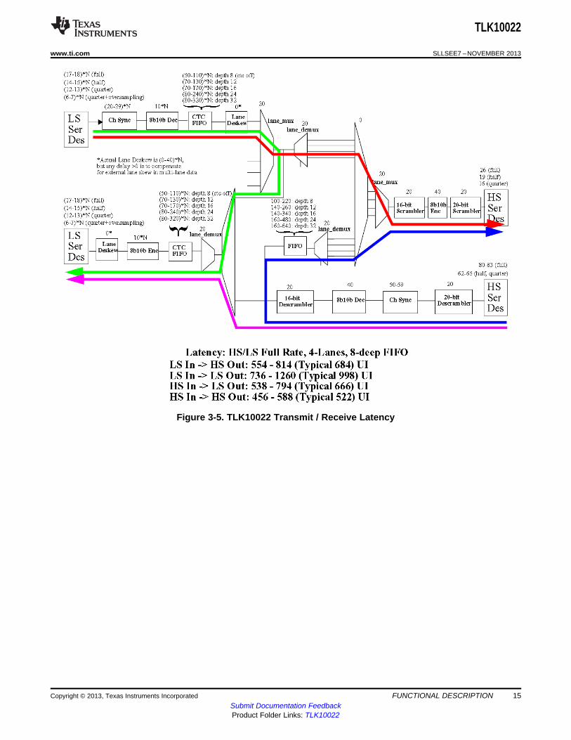
3.4.7 Transmit / Receive LatencyThe latency through the TLK10022 is shown in Figure 3-5. Note that the latency ranges shown indicatestatic rather than dynamic latency variance, i.e., the range of possible latencies when the serial link isinitially established. During normal operation, the latency through the device is fixed.
14 FUNCTIONAL DESCRIPTION Copyright © 2013, Texas Instruments IncorporatedSubmit Documentation FeedbackProduct Folder Links: TLK10022
TLK10022
www.ti.com SLLSEE7 –NOVEMBER 2013
Figure 3-5. TLK10022 Transmit / Receive Latency
Copyright © 2013, Texas Instruments Incorporated FUNCTIONAL DESCRIPTION 15Submit Documentation FeedbackProduct Folder Links: TLK10022

HSTXAP
HSTXAN
HSRXAP
HSRXAN
TRANSMITTER RECEIVERMEDIA
50
50
50 ohm transmission line
50 ohm transmission line
GND
VTERM
TLK10022
SLLSEE7 –NOVEMBER 2013 www.ti.com
4 SERDES INTERFACES
This section describes the high speed I/O that are used to transmit and receive the aggregated data.
4.1 High Speed CML OutputThe high speed data output driver is implemented using Current Mode Logic (CML) with integrated pull upresistors, requiring no external components. The transmit outputs must be AC coupled.
Figure 4-1. Example of High Speed I/O AC Coupled Mode (Channel A HS side is shown)
Current Mode Logic (CML) drivers often require external components. The disadvantage of the externalcomponent is a limited edge rate due to package and line parasitic. The CML driver on TLK10022 has on-chip 50Ω termination resistors terminated to VDDT, providing optimum performance for increased speedrequirements. The transmitter output driver is highly configurable allowing output amplitude and de-emphasis to be tuned to a channel's individual requirements. Software programmability allows for veryflexible output amplitude control. Only AC coupled output mode is supported.
When transmitting data across long lengths of PCB trace or cable, the high frequency content of the signalis attenuated due to the skin effect of the media. This causes a “smearing” of the data eye when viewedon an oscilloscope. The net result is reduced timing margins for the receiver and clock recovery circuits. Inorder to provide equalization for the high frequency loss, 4-tap finite impulse response (FIR) transmit de-emphasis is implemented. A highly configurable output driver maximizes flexibility in the end system byallowing de-emphasis and output amplitude to be tuned to a channel’s individual requirements. Outputswing is selectable via MDIO.
See Figure 7-2 output waveform flexibility. The level of de-emphasis is programmable via the MDIOinterface through control registers (5.7:4 and 5.12:8) through pre-cursor and post-cursor settings. Userscan control the strength of the de-emphasis to optimize for a specific system requirement.
4.2 High Speed ReceiverThe high speed receiver is implemented using differential CML with internal termination resistors. Thereceiver requires AC coupling. The termination impedances of the receivers are configured as 100 Ω withthe center tap weakly tied to 0.7×VDDT, and a capacitor to create an AC ground.
TLK10022 serial receivers incorporate adaptive equalizers. This circuit compensates for channel insertionloss by amplifying the high frequency components of the signal, reducing inter-symbol interference.Equalization can be enabled or disabled per register settings. Both feed-forward equalization (FFE) anddecision feedback equalization (DFE) are used to minimize the pre-cursor and post-cursor components(respectively) of intersymbol interference.
16 SERDES INTERFACES Copyright © 2013, Texas Instruments IncorporatedSubmit Documentation FeedbackProduct Folder Links: TLK10022

TLK10022
www.ti.com SLLSEE7 –NOVEMBER 2013
4.3 Loss of Signal Output Signal Generation (LOS)Loss of input signal detection is based on the voltage level of each serial input signal INA×P/N, INB×P/N,HSRXAP/N, and HSRXBP/N. Anytime the serial receive input differential signal peak to peak voltage levelis ≤75 mVpp for High Speed side or ≤65mVpp for Low Speed side, LOSA or LOSB are asserted (high true)respectively for Channel A and Channel B (if enabled, disabled by default). Note that an input signal ≥150mVpp for High Speed side and ≥175 mVpp for Low Speed side is required for reliable operation of the lossof signal detection circuits. If the input signal is between these two ranges, the SERDES will operateproperly, but the LOS indication will not be valid (or robust). The LOS indications are also directly readablethrough the MDIO interface in respective registers.
The following additional critical status conditions can be combined with the loss of signal conditionenabling additional real-time status signal visibility on the LOSA and LOSB outputs per channel:1. Loss of Channel Synchronization Status – Logically OR’d with LOS condition(s) when enabled. Loss of
channel synchronization can be optionally logically OR’d (disabled by default) with the internallygenerated LOS condition (per channel).
2. Loss of PLL Lock Status on LS and HS sides – Logically OR’d with LOS condition(s) when enabled.The internal PLL loss of lock status bit is optionally OR’d (disabled by default) with the other internallygenerated loss of signal conditions (per channel).
3. Receive 8B/10B Decode Error (Invalid Code Word or Running Disparity Error) – Logically OR’d withLOS condition(s) when enabled. The occurrence of an 8B/10B decode error (invalid code word ordisparity error) is optionally OR’d (disabled by default) with the other internally generated loss of signalconditions (per channel).
4. AGCLOCK (Active Gain Control Currently Locked) – Inverted and Logically OR’d with LOS condition(s)when enabled. HS RX SERDES adaptive gain control unlocked indication is optionally OR’d (disabledby default) with the other internally generated loss of signal conditions (per channel).
5. AZDONE (Auto Zero Calibration Done) – Inverted and Logically OR’d with LOS conditions(s) whenenabled. HS RX SERDES auto-zero not done indication is optionally OR’d (disabled by default) withthe other internally generated loss of signal conditions (per channel).
Copyright © 2013, Texas Instruments Incorporated SERDES INTERFACES 17Submit Documentation FeedbackProduct Folder Links: TLK10022

TLK10022
SLLSEE7 –NOVEMBER 2013 www.ti.com
5 CLOCKING
5.1 Configuring PLL and Line RatesThe TLK10022 includes internal low-jitter high quality oscillators that are used as frequency multipliers forthe low speed and high speed SERDES and other internal circuits of the device. Specific MDIO registersare available for SERDES rate and PLL multiplier selection to match line rates and reference clock(REFCLK0/1) frequencies for various applications. Some examples are detailed below on how to selectand configure.
The external differential reference clock has a large operating frequency range allowing support for manydifferent applications. The reference clock frequency must be within ±200 PPM of the incoming serial datarate (±100 PPM of nominal data rate).
Table 5-1. Line Rate and Reference Clock Frequency Ranges for the Low Speed Side SERDESREFERENCE CLOCK (MHz) FULL RATE (Gbps) HALF RATE (Gbps) QUARTER RATE (Gbps)SERDES PLL
MULTIPLIER (MPY) MIN MAX MIN MAX MIN MAX MIN MAX
4 250 425 2 3.4 1 1.7 0.5 0.85
5 200 425 2 4.25 1 2.125 0.5 1.0625
6 166.667 416.667 2 5 1 2.5 0.5 1.25
8 125 312.5 2 5 1 2.5 0.5 1.25
10 122.88 250 2.4576 5 1.2288 2.5 0.6144 1.25
12 122.88 208.333 2.94912 5 1.47456 2.5 0.73728 1.25
12.5 122.88 200 3.072 5 1.536 2.5 0.768 1.25
15 122.88 166.667 3.6864 5 1.8432 2.5 0.9216 1.25
20 122.88 125 4.9152 5 2.4576 2.5 1.2288 1.25
Rate Scale: Full Rate = 0.5, Half Rate = 1, Quarter Rate = 2
Table 5-2. Line Rate and Reference Clock Frequency Ranges for the High Speed Side SERDESREFERENCE CLOCK FULL RATE HALF RATE QUARTER RATE EIGHTH RATE
SERDES PLL (MHz) (Gbps) (Gbps) (Gbps) (Gbps)MULTIPLIER (MPY)
MIN MAX MIN MAX MIN MAX MIN MAX MIN MAX
4 375 425 6 6.8 3 3.4 1.5 1.7
5 300 425 6 8.5 3 4.25 1.5 2.125 1 1.0625
6 250 416.667 6 10 3 5 1.5 2.5 1 1.25
8 187.5 312.5 6 10 3 5 1.5 2.5 1 1.25
10 150 250 6 10 3 5 1.5 2.5 1 1.25
12 125 208.333 6 10 3 5 1.5 2.5 1 1.25
15 122.88 166.667 7.3728 10 3.6864 5 1.8432 2.5 1 1.25
16 122.88 156.25 7.864 10 3.932 5 1.966 2.5 1 1.25
20 122.88 125 9.8304 10 4.9152 5 2.4576 2.5 1.2288 1.25
Rate Scale: Full Rate = 0.25, Half Rate = 0.5, Quarter Rate = 1, Eighth Rate = 2
5.1.1 4:1 Reference Clock Frequency Selection ExampleIn the 4:1 operation mode, if the low speed side line rate is 2.2Gbps, the high-speed side line rate will be8.8Gbps. The following steps can be taken to make a reference clock frequency selection:1. Determine the appropriate SERDES rate modes that support the required line rates. Table 5-1 shows
that the 2.2Gbps line rate on the low speed side is supported in the half rate mode (RateScale = 1)and in the full rate mode (RateScale = 0.5). In the first example, half rate will be used. Table 5-2 showsthat the 8.8Gbps line rate on the high speed side is only supported in the full rate mode (RateScale =0.25).
2. For each SERDES side, and for all available PLL multipliers (MPY), compute the correspondingreference clock frequencies using the formula:
18 CLOCKING Copyright © 2013, Texas Instruments IncorporatedSubmit Documentation FeedbackProduct Folder Links: TLK10022

TLK10022
www.ti.com SLLSEE7 –NOVEMBER 2013
Reference Clock Frequency = (LineRate × RateScale)/MPY
The computed reference clock frequencies are shown in Table 5-3 along with the valid minimum andmaximum frequency values.
3. Mark all the common frequencies that appear on both SERDES sides. Note and discard all those thatfall outside the allowed range. In this example, the common frequencies are highlighted in Table 5-3.
4. Select any of the remaining marked common reference clock frequencies. The higher the referenceclock frequency usually the better. In this example, any of the following reference clock frequenciescan be selected: 366.67MHz, 275MHz, 220MHz, 183.33MHz, and 146.67MHz.
Table 5-3. Reference Clock Frequency Selection Example
LOW SPEED SIDE SERDES HIGH SPEED SIDE SERDESREFERENCE CLOCK FREQUENCY REFERENCE CLOCK FREQUENCY
SERDES PLL SERDES PLL(MHz) (MHz)MULTIPLIER MULTIPLIER
COMPUTED MIN MAX COMPUTED MIN MAX4 550 250 425 4 550 375 4255 440 200 425 5 440 300 4256 366.67 166.667 416.667 6 366.67 250 4258 275 125 312.5 8 275 187.5 390.62510 220 122.88 250 10 220 150 312.512 183.33 122.88 208.333 12 183.33 125 260.41715 146.67 122.88 166.667 15 146.67 122.88 208.33320 110 122.88 125 16 137.5 122.88 195.3125
20 110 122.88 156.25
5.1.2 2:1 Reference Clock Frequency Selection ExampleNow take the same low speed rate and configure the device for 2:1 operation, so the high speed side isnow 4.4Gbps. Based on the Line Rate/Reference Clock table, the only rate available at 4.4Gbps is HalfRate, so the rate scale is 0.5. The High Speed Side SERDES table is unchanged from the 4:1 mode(8.8Gbps x 0.25 in 4:1 mode, versus 4.4Gbps x 0.5 in 2:1 mode).
For the next example, using the same date rates and 4:1 mode, full rate will be chosen for the low speedside. The matching reference clock frequencies are 275MHz, 220MHz, 183.33MHz and 137.5MHz.
spacerLOW SPEED SIDE SERDES HIGH SPEED SIDE SERDES
REFERENCE CLOCK FREQUENCY REFERENCE CLOCK FREQUENCYSERDES PLL SERDES PLL(MHz) (MHz)MULTIPLIER MULTIPLIER
COMPUTED MIN MAX COMPUTED MIN MAX4 275 250 425 4 550 375 4255 220 200 425 5 440 300 4256 183.33 166.667 416.667 6 366.67 250 4258 137.5 125 312.5 8 275 187.5 390.62510 110 122.88 250 10 220 150 312.512 91.67 122.88 208.333 12 183.33 125 260.41715 73.33 122.88 166.667 15 146.67 122.88 208.33320 55 122.88 125 16 137.5 122.88 195.3125
20 110 122.88 156.25
Copyright © 2013, Texas Instruments Incorporated CLOCKING 19Submit Documentation FeedbackProduct Folder Links: TLK10022

TLK10022
SLLSEE7 –NOVEMBER 2013 www.ti.com
5.1.3 3:1 Mode ConfigurationIn 3:1 mode, there are only two possible combinations of low speed SERDES and high speed SERDESPLL multipliers. One option is Low Speed multiplier 10x and High Speed multiplier 15x, and the other isLow Speed multiplier 8x and High Speed Multiplier 12x. Select a REFCLK frequency that works best forthe application.
5.1.4 Low Speed Side Rates Below 500Mbps (4:1 mode only)For serial links below 500Mbps, the Low Speed Side SERDES must be configured using twice the desireddata rate. For instance, 270Mbps data must be configured for 540Mbps. In addition, the device must beconfigured through MDIO to run at half speed. This enables over-sampling of data to support data rateslower than the Low Speed side SERDES IP allows. Note that the High Speed SERDES should beconfigured for the actual data rate, and not 2x. Using the same 270Mbps example, the high speed sideshould be configured for 0.27x4 = 1.08Gbps.
Also note that Low Speed side rate will be twice the High Speed rate, and the High Speed PLL multiplierwill be 2x of Low Speed. For 270Mbps/1.08Gbps and a REFCLK of 135MHz, the Low Speed side will beset to 8x, Quarter Rate (540MHz) and the High Speed side will be set to 16x, Eighth Rate (1.08Gbps).
5.2 Clocking ArchitectureA simplified clocking architecture for the TLK10022 is captured in Figure 5-1. Each channel (Channel A orChannel B) has an option of operating with a differential reference clock provided either on pinsREFCLK0P/N or REFCLK1P/N. The choice is made either through MDIO or through REFCLKA_SEL andREFCLKB_SEL pins. The reference clock frequencies for those two clock inputs can be different as longas they fall under the valid ranges shown in Table 5-2. For each channel, the low speed side SERDES,high speed side SERDES and the associated part of the digital core operate from the same referenceclock.
The clock and data recovery (CDR) function of the high speed side receiver recovers the clock from theincoming serial data. The high speed side SERDES makes available two versions of clocks for furtherprocessing:1. HS_RXBCLK_A/B: recovered byte clock synchronous with incoming serial data and with a frequency
matching the incoming line rate divided by 20.2. VCO_CLOCK_A/B_DIV2: VCO frequency divided by 2. (VCO frequency = REFCLK x PLL Multiplier).
The above-mentioned clocks can be output through the differential pins, CLKOUTAP/N andCLKOUTBP/N, with optional frequency division ratios of 1, 2, 4, 5, 8, 10, 16, 20, or 25. The clock outputoptions are software controlled through the MDIO interface register 0x15. The maximum CLKOUTfrequency is 500MHz.
20 CLOCKING Copyright © 2013, Texas Instruments IncorporatedSubmit Documentation FeedbackProduct Folder Links: TLK10022

INA[3:0]P/N
OUTA[3:0]P/N
Low
Speed
Side
SERDES
Channel A
HSTXAP/N
HSRXAP/N
High
Speed
Side
SERDES
Channel A
+
_
+
_
REFCLK0P/N
REFCLK1P/N
+
_CLKOUTAP/N
INB[3:0]P/N
OUTB[3:0]P/N
Low
Speed
Side
SERDES
Channel B
HSTXBP/N
HSRXBP/N
High
Speed
Side
SERDES
Channel B
+
_CLKOUTBP/N
A S/W
Reg: 1.3:2
Reg: 1.7:4
Divide by N
(N=1,2,4,5,8,
10,16,20,25)
Divide by N
(N=1,2,4,5,8,
10,16,20,25)
HS_RXBCLK_A
VCO_CLOCK_A_DIV2
HS_RXBCLK_B
VCO_CLOCK_B_DIV2
4
2
B S/W
Reg: 1.3:2
Reg: 1.7:4
4
2REFCLKB_SEL
REFCLKA_SEL
TLK10022
www.ti.com SLLSEE7 –NOVEMBER 2013
Figure 5-1. Clocking Architecture
Copyright © 2013, Texas Instruments Incorporated CLOCKING 21Submit Documentation FeedbackProduct Folder Links: TLK10022

> 32 "1's"
0 1 1PA[4:0] D15 D00 1 0
Idle
1
StartWriteCode
PHYAddr
TurnAround
DataREGAddr
RA4 RA0
Preamble
MDC
MDIO
> 32 "1's"
0 1 ZPA[4:0] D15 D01 0 0
Idle
1
StartReadCode
PHYAddr
TurnAround
DataREGAddr
RA4 RA0
Preamble
MDC
MDIO
TLK10022
SLLSEE7 –NOVEMBER 2013 www.ti.com
6 PROGRAMMERS REFERENCE
Channel identification is based on PHY (Port) address field. Channel A can be accessed by setting LSB ofPHY address to 0. Channel B can be accessed by setting LSB of PHY address to 1.
6.1 MDIO Management InterfaceThe TLK10022 supports the Management Data Input/Output (MDIO) Interface as defined in Clause 22 ofthe IEEE 802.3 Ethernet specification. The MDIO allows register-based management and control of theserial links. Normal operation of the TLK10022 is possible without use of this interface. However, somefeatures are accessible only through the MDIO.
The MDIO Management Interface consists of a bi-directional data path (MDIO) and a clock reference(MDC). The port address is determined by control pins PRTAD[4:0] as described in Table 2-1.
In Clause 22, the top 4 control pins PRTAD[4:1] determine the device port address. In this mode the 2individual channels in TLK10022 are classified as 2 different ports. So for any PRTAD[4:1] value there willbe 2 ports per TLK10022.
TLK10022 will respond if the 4 MSB’s of PHY address field on MDIO protocol (PA[4:1]) matchesPRTAD[4:1]. The LSB of PHY address field (PA[0]) will determine which channel/port within TLK10022 torespond to.
If PA[0] = 1b0, TLK10022 Channel A will respond.
If PA[0] = 1b1, TLK10022 Channel B will respond.
Write transactions which address an invalid register or device or a read only register will be ignored. Readtransactions which address an invalid register will return a 0.
MDIO Protocol Timing: The Clause 22 timing required to read from the internal registers is shown inFigure 6-1. The Clause 22 timing required to write to the internal registers is shown in Figure 6-2.
Note that the 1 in the Turn Around section is externally pulled up, and driven to Z by TLK10022.
Figure 6-1. CL22 - Management Interface Read Timing
Figure 6-2. CL22 - Management Interface Write Timing
22 PROGRAMMERS REFERENCE Copyright © 2013, Texas Instruments IncorporatedSubmit Documentation FeedbackProduct Folder Links: TLK10022

> 32 "1's"
0 1 ZPA[4:0] D15 D01 0 0
Idle
1
StartReadCode
PHYAddr
TurnAround
DataREGAddr
5'h1F
Preamble
MDC
MDIO
> 32 "1's"
0 1 1PA[4:0] 16'h90000 1 0
Idle
1
StartWriteCode
PHYAddr
TurnAround
DataREGAddr
5'h1E
Preamble
MDC
MDIO
> 32 "1's"
0 1 1PA[4:0] DATA0 1 0
Idle
1
StartWriteCode
PHYAddr
TurnAround
DataREGAddr
5'h1F
Preamble
MDC
MDIO
> 32 "1's"
0 1 1PA[4:0] 16'h90000 1 0
Idle
1
StartWriteCode
PHYAddr
TurnAround
DataREGAddr
5'h1E
Preamble
MDC
MDIO
TLK10022
www.ti.com SLLSEE7 –NOVEMBER 2013
Clause 22 Indirect Addressing: The TLK10022 Register space is divided into two register groups. Oneregister group can be addressed directly through Clause 22, and one register group can be addressedindirectly through Clause 22. The register group which can be addressed through Clause 22 indirectly isimplemented in vendor specific register space (16’h8000 onwards). Due to clause 22 register spacelimitations, an indirect addressing method is implemented so that this extended register space can beaccessed through clause 22. To access this register space (16’h8000 onwards), an address controlregister (Reg 30, 5’h1E) should be written with the register address followed by a read/write transaction toaddress data register (Reg 31, 5’h1F) to access the contents of the address specified in address controlregister.
The following timing diagrams illustrate an example write transaction to Register 16’h8000 using indirectaddressing in Clause 22.
Figure 6-3. CL22 – Indirect Address Method – Address Write
Figure 6-4. CL22 - Indirect Address Method – Data Write
The following timing diagrams illustrate an example read transaction to read contents of Register 16’h8000using indirect addressing in Clause 22.
Figure 6-5. CL22 - Indirect Address Method – Address Write
Note that the 1 in the Turn Around section is externally pulled up, and driven to Z by TLK10022.
Figure 6-6. CL22 - Indirect Address Method – Data Read
Copyright © 2013, Texas Instruments Incorporated PROGRAMMERS REFERENCE 23Submit Documentation FeedbackProduct Folder Links: TLK10022

TLK10022
SLLSEE7 –NOVEMBER 2013 www.ti.com
6.2 Register Bit DefinitionsRW: Read-WriteUser can write 0 or 1 to this register bit. Reading this register bit returns the same value that has beenwritten.
RW/SC: Read-Write Self-ClearingUser can write 0 or 1 to this register bit. Writing a "1" to this register creates a high pulse. Reading thisregister bit always returns 0.
RO: Read-OnlyThis register can only be read. Writing to this register bit has no effect. Reading from this register bitreturns its current value.
RO/LH: Read-Only Latched HighThis register can only be read. Writing to this register bit has no effect. Reading a "1" from this register bitindicates that either the condition is occurring or it has occurred since the last time it was read. Reading a"0" from this register bit indicates that the condition is not occurring presently, and it has not occurredsince the last time the register was read. A latched high register, when read high, should be read again todistinguish if a condition occurred previously or is still occurring. If it occurred previously, the second readwill read low. If it is still occurring, the second read will read high. Reading this register bit automaticallyresets its value to 0.
RO/LL: Read-Only Latched LowThis register can only be read. Writing to this register bit has no effect. Reading a "0" from this register bitindicates that either the condition is occurring or it has occurred since the last time it was read. Reading a"1" from this register bit indicates that the condition is not occurring presently, and it has not occurredsince the last time the register was read. A latched low register, when read low, should be read again todistinguish if a condition occurred previously or is still occurring. If it occurred previously, the second readwill read high. If it is still occurring, the second read will read low. Reading this register bit automaticallysets its value to 1.
COR: Clear-On-ReadThis register can only be read. Writing to this register bit has no effect. Reading from this register bitreturns its current value, then resets its value to 0. Counter value freezes at Max.
The following registers can be accessed directly through Clause 22.
24 PROGRAMMERS REFERENCE Copyright © 2013, Texas Instruments IncorporatedSubmit Documentation FeedbackProduct Folder Links: TLK10022

TLK10022
www.ti.com SLLSEE7 –NOVEMBER 2013
Table 6-1. GLOBAL_CONTROL_1 (1)
Register Address:0x00 SPACER Default: 0x0610Bit(s) Name Description Access
15 GLOBAL_RESET Global reset. RW0 = Normal operation (Default 1’b0) SC (2)
1 = Resets TX and RX data path including MDIO registers. Equivalent to assertingRESET_N.
14:13 RESERVED For TI use only. Always reads 0. RW12 RESERVED For TI use only (Default 1'b0) RW11 GLOBAL_WRITE Global write enable. RW
0 = Control settings are specific to channel addressed (Default 1’b0)1 = Control settings in channel specific registers are applied to both channelsregardless of channel addressed
10:7 RESERVED For TI use only (Default 4’b1100) RW6:5 RESERVED For TI use only. Always reads 0.4:0 PRBS_PASS_OVERLAY[4:0] PRBS_PASS pin status selection. Applicable only when PRBS test pattern RW
verification is enabled on HS side or LS side.PRBS_PASS pin reflects PRBS verification status on selected Channel HS/LS side.1xx00 = PRBS_PASS reflects combined status of Channel A/B HS serdes PRBSverification. If PRBS verification fails on any channel HS serdes, PRBS_PASS will beasserted low. (Default 5’b10000)00000 = Status from Channel A HS Serdes side00001 = Reserved Status from Channel A HS core side0001x = Reserved00100 = Status from Channel A LS Serdes side Lane 000101 = Status from Channel A LS Serdes side Lane 100110 = Status from Channel A LS Serdes side Lane 200111 = Status from Channel A LS Serdes side Lane 301000 = Status from Channel B HS Serdes side01001 = Reserved Status from Channel B HS core side0101x = Reserved01100 = Status from Channel B LS Serdes side Lane 001101 = Status from Channel B LS Serdes side Lane 101110 = Status from Channel B LS Serdes side Lane 201111 = Status from Channel B LS Serdes side Lane 3
(1) This global register is channel independent.(2) After reset bit is set to one, it automatically sets itself back to zero on the next MDC clock cycle.
Copyright © 2013, Texas Instruments Incorporated PROGRAMMERS REFERENCE 25Submit Documentation FeedbackProduct Folder Links: TLK10022

TLK10022
SLLSEE7 –NOVEMBER 2013 www.ti.com
Table 6-2. CHANNEL_CONTROL_1
Register Address:0x01 SPACER Default: 0x4000Bit(s) Name Description Access
15 POWERDOWN Setting this bit high powers down entire data path with exception that MDIO RWinterface stays active.0 = Normal operation (Default 1’b0)1 = Power Down mode is enabled.
14 LT_ENABLE 1 = Enable link training (Default 1’b1) RW0 = Disable link trainingThis bit should be set to HIGH for auto train mode to function correctly
13:10 RESERVED For TI use only (Default 4’b0000) RW9 RX_BIT_INTERLEAVE 0 = Normal operation. (Default 1’b0) RW
1 = Enable bit interleave on receive path8 TX_BIT_INTERLEAVE 0 = Normal operation. (Default 1’b0) RW
1 = Enable bit interleave on transmit path7:6 RX_MODE_SEL Receive datapath mode RO
00 = 4 lane mode (Default 2’b00)01 = 2 lane mode1x = 3 lane mode
5:4 TX_MODE_SEL Transmit datapath mode RW00 = 4 lane mode (Default 2’b00)01 = 2 lane mode1x = 3 lane mode
3 RX_1LN_MODE_SEL 0 = Rx datapath mode selected through RX_MODE_SEL(Default 1’b0) RW1 = Enable 1 lane mode on receive datapath
2 TX_1LN_MODE_SEL 0 = Tx datapath mode selected through TX_MODE_SEL(Default 1’b0) RW1 = Enable 1 lane mode on transmit datapath
1 REFCLK_SW_SEL Channel HS Reference clock selection. Applicable only when REFCLK_SEL pin is RWLOW.0 = Selects REFCLK_0_P/N as clock reference to Channel x HS side serdesmacro(Default 1’b0)1 = Selects REFCLK_1_P/N as clock reference to Channel x HS side serdes macro
0 LS_REFCLK_SEL Channel LS Reference clock selection. RW0 = LS side serdes macro reference clock is same as HS side serdes referenceclock (E.g. If REFCLK_0_P/N is selected as HS side serdes macro reference clock,REFCLK_0_P/N is selected as LS side serdes macro reference clock and viceversa) (Default 1’b0)1 = Alternate reference clock is selected as clock reference to Channel x LS sideserdes macro (E.g. If REFCLK_0_P/N is selected as HS side serdes macroreference clock, REFCLK_1_P/N is selected as LS side serdes macro referenceclock and vice versa)
26 PROGRAMMERS REFERENCE Copyright © 2013, Texas Instruments IncorporatedSubmit Documentation FeedbackProduct Folder Links: TLK10022

TLK10022
www.ti.com SLLSEE7 –NOVEMBER 2013
Table 6-3. HS_SERDES_CONTROL_1
Register Address:0x02 SPACER Default: 0x831DBit(s) Name Description Access15:10 RESERVED For TI use only (Default 6’b100000) RW9:8 HS_LOOP_BANDWIDTH[1:0] HS Serdes PLL Loop Bandwidth settings RW
00 = Medium Bandwidth01 = Low Bandwidth10 = High Bandwidth11 = Ultra High Bandwidth. (Default 2'b11)
7 RESERVED For TI use only (Default 1’b0) RW6 HS_VRANGE HS Serdes PLL VCO range selection. RW
0 = VCO runs at higher end of frequency range (Default 1’b0)1 = VCO runs at lower end of frequency rangeThis bit needs to be set HIGH if VCO frequency (REFCLK *HS_PLL_MULT) isbelow 2.5 GHz.
5 RESERVED For TI use only (Default 1’b0) RW4 HS_ENPLL HS Serdes PLL enable control. HS Serdes PLL is automatically disabled when RW
PD_TRXx_N is asserted LOW or when register bit 1.15 is set HIGH.0 = Disables PLL in HS serdes1 = Enables PLL in HS serdes (Default 1’b1)
3:0 HS_PLL_MULT[3:0] HS Serdes PLL multiplier setting (Default 4’b1101). RWRefer to Table 6-4
Table 6-4. HS PLL Multiplier Control
2.3:0 2.3:0PLL MULTIPLIER PLL MULTIPLIERVALUE VALUEFACTOR FACTOR
0000 Reserved 1000 12x0001 Reserved 1001 12.5x0010 4x 10¹⁰ 15x0011 5x 10¹¹ 16x0100 6x 1100 16.5x0101 8x 1101 20x0110 8.25x 1110 25x0111 10x 1111 Reserved
Copyright © 2013, Texas Instruments Incorporated PROGRAMMERS REFERENCE 27Submit Documentation FeedbackProduct Folder Links: TLK10022

TLK10022
SLLSEE7 –NOVEMBER 2013 www.ti.com
Table 6-5. HS_SERDES_CONTROL_2
Register Address:0x03 SPACER Default:0xA848Bit(s) Name Description Access15:12 HS_SWING[3:0] Transmitter Output swing control for HS Serdes. (Default 4’b1010) RW
Refer to Table 6-611 HS_ENTX HS Serdes transmitter enable control. HS Serdes transmitter is automatically disabled RW
when PD_TRXx_N is asserted LOW or when register bit 1.15 is set HIGH.0 = Disables HS serdes transmitter1 = Enables HS serdes transmitter (Default 1’b1)
10 HS_EQHLD HSRX Equalizer hold control. RW0 = Normal operation (Default 1’b0)1 = Holds equalizer and long tail correction in its current state
9:8 HS_RATE_TX [1:0] HS Serdes TX rate settings. RW00 = Full rate (Default 2’b00)01 = Half rate10 = Quarter rate11 = Eighth rate
7:6 HS_AGCCTRL[1:0] Adaptive gain control loop. RW00 = Attenuator will not change after lock has been achieved, even if AGC becomesunlocked01 = Attenuator will not change when in lock state, but could change when AGCbecomes unlocked (Default 2’b01)10 = Force the attenuator off11 = Force the attenuator on
5:4 HS_AZCAL[1:0] Auto zero calibration. RW00 = Auto zero calibration initiated when receiver is enabled (Default 2’b00)01 = Auto zero calibration disabled10 = Forced with automatic update.11 = Forced without automatic update
3 HS_ENRX HS Serdes receiver enable control. RWHS Serdes receiver is automatically disabled when PD_TRXx_N is asserted LOW orwhen register bit 1.15 is set HIGH.0 = Disables HS serdes receiver1 = Enables HS serdes receiver (Default 1’b1)
2:0 HS_RATE_RX [2:0] HS Serdes RX rate settings. RW000 = Full rate (Default 3’b000)101 = Half rate110 = Quarter rate111 = Eighth rate001 = Reserved01x = Reserved100 = Reserved
Table 6-6. HSTX AC Mode Output Swing Control
AC MODEVALUE3[15:12] TYPICAL AMPLITUDE (mVdfpp)
0000 1300001 2200010 3000011 3900100 4800101 5700110 6600111 7501000 8301001 9301010 10201011 1110
28 PROGRAMMERS REFERENCE Copyright © 2013, Texas Instruments IncorporatedSubmit Documentation FeedbackProduct Folder Links: TLK10022

TLK10022
www.ti.com SLLSEE7 –NOVEMBER 2013
Table 6-6. HSTX AC Mode Output Swing Control (continued)AC MODEVALUE
3[15:12] TYPICAL AMPLITUDE (mVdfpp)1100 11801101 12701110 13401111 1400
Table 6-7. HS_SERDES_CONTROL_3
Register Address:0x04 SPACER Default:0x1500Bit(s) Name Description Access15 HS_ENTRACK HSRX ADC Track mode. RW
0 = Normal operation (Default 1’b0)1 = Forces ADC into track mode
14:12 HS_EQPRE[2:0] Serdes Rx precursor equalizer selection RW000 = 1/9 cursor amplitude001 = 3/9 cursor amplitude (Default 3’b001)010 = 5/9 cursor amplitude011 = 7/9 cursor amplitude100 = 9/9 cursor amplitude101 =11/9 cursor amplitude110 = 13/9 cursor amplitude111 = Disable
11:10 HS_CDRFMULT[:10] Clock data recovery algorithm frequency multiplication selection (Default 2'b01) RW00 = First order. Frequency offset tracking disabled01 = Second order. 1x mode10 = Second order. 2x mode11 = Reserved
9:8 HS_CDRTHR[1:0] Clock data recovery algorithm threshold selection (Default 2'b01) RW00 = Four vote threshold01 = Eight vote threshold10 = Sixteen vote threshold11 = Thirty two vote threshold
7 RESERVED For TI use only (Default 1’b0) RW6 HS_PEAK_DISABLE HS Serdes PEAK_DISABLE control RW
0 = Normal operation (Default 1’b0)1 = Disables high frequency peaking. Suitable for <6 Gbps operation
5 HS_H1CDRMODE HS_Serdes H1CDRMODE control RW0 = Normal operation (Default 1’b0)1 = Enables CDR mode suitable for short channel operation.
4:0 HS_TWCRF[4:0] Cursor Reduction Factor (Default 5’b00000). Refer to Table 6-8. RW
Copyright © 2013, Texas Instruments Incorporated PROGRAMMERS REFERENCE 29Submit Documentation FeedbackProduct Folder Links: TLK10022

TLK10022
SLLSEE7 –NOVEMBER 2013 www.ti.com
Table 6-8. HSTX Cursor Reduction Factor Weights
4.4:0 4.4:0CURSOR REDUCTION CURSOR REDUCTIONVALUE VALUE(%) (%)
00000 0 10000 1700001 2.5 10001 2000010 5.0 10010 2200011 7.5 10011 2500100 10.0 10100 2700101 12 10101 3000110 15 10110 3200111 10111 3501000 11000 3701001 11001 4001010 11010 4201011 Reserved 11011 4501100 11100 4701101 11101 5001110 11110 5201111 11111 55
Table 6-9. HS_SERDES_CONTROL_4
Register Address:0x05 SPACER SPACERDefault:0x2000Bit(s) Name Description Access15 HS_RX_INVPAIR Receiver polarity. RW
0 = Normal polarity. HSRXxP considered positive data. HSRXxN considered negative data(Default 1’b0)1 = Inverted polarity. HSRXxP considered negative data. HSRXxN considered positive data
14 HS_TX_INVPAIR Transmitter polarity. RW0 = Normal polarity. HSTXxP considered positive data and HSTXxN considered negativedata (Default 1’b0)1 = Inverted polarity. HSTXxP considered negative data and HSTXxN considered positivedata
13 RESERVED For TI use only (Default 1’b1) RW12:8 HS_TWPOST1[4:0] Adjacent post cursor1 Tap weight. Selects TAP settings for TX waveform. RW
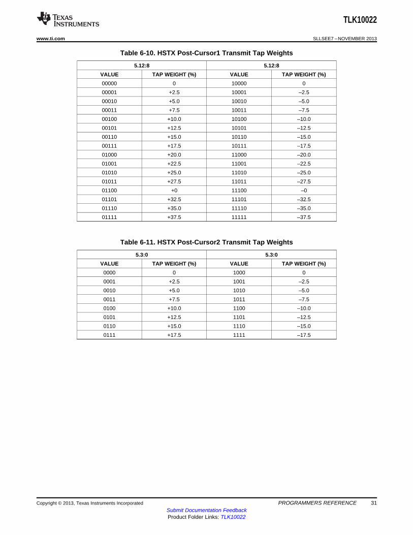
(Default 5’b00000 ) Refer Table 6-10.7:4 HS_TWPRE[3:0] Precursor Tap weight. Selects TAP settings for TX waveform. RW
(Default 4’b0000) Refer Table 6-12.3:0 HS_TWPOST2[3:0] Adjacent post cursor2 Tap weight. Selects TAP settings for TX waveform. RW
(Default 4’b0000) Refer Table 6-11.
30 PROGRAMMERS REFERENCE Copyright © 2013, Texas Instruments IncorporatedSubmit Documentation FeedbackProduct Folder Links: TLK10022
TLK10022
www.ti.com SLLSEE7 –NOVEMBER 2013
Table 6-10. HSTX Post-Cursor1 Transmit Tap Weights
5.12:8 5.12:8VALUE TAP WEIGHT (%) VALUE TAP WEIGHT (%)00000 0 10000 000001 +2.5 10001 –2.500010 +5.0 10010 –5.000011 +7.5 10011 –7.500100 +10.0 10100 –10.000101 +12.5 10101 –12.500110 +15.0 10110 –15.000111 +17.5 10111 –17.501000 +20.0 11000 –20.001001 +22.5 11001 –22.501010 +25.0 11010 –25.001011 +27.5 11011 –27.501100 +0 11100 –001101 +32.5 11101 –32.501110 +35.0 11110 –35.001111 +37.5 11111 –37.5
Table 6-11. HSTX Post-Cursor2 Transmit Tap Weights
5.3:0 5.3:0VALUE TAP WEIGHT (%) VALUE TAP WEIGHT (%)
0000 0 1000 00001 +2.5 1001 –2.50010 +5.0 1010 –5.00011 +7.5 1011 –7.50100 +10.0 1100 –10.00101 +12.5 1101 –12.50110 +15.0 1110 –15.00111 +17.5 1111 –17.5
Copyright © 2013, Texas Instruments Incorporated PROGRAMMERS REFERENCE 31Submit Documentation FeedbackProduct Folder Links: TLK10022

TLK10022
SLLSEE7 –NOVEMBER 2013 www.ti.com
Table 6-12. HSTX Pre-Cursor Transmit Tap Weights
5.7:4 5.7:4VALUE TAP WEIGHT (%) VALUE TAP WEIGHT (%)
0000 0 1000 00001 +2.5 1001 –2.50010 +5.0 1010 –5.00011 +7.5 1011 –7.50100 +10.0 1100 –10.00101 +12.5 1101 –12.50110 +15.0 1110 –15.00111 +17.5 1111 –17.5
Table 6-13. LS_SERDES_CONTROL_1
Register Address:0x06 SPACER Default:0x8115Bit(s) Name Description Access15 GLOBAL_LN_WRITE Global lane write enable. RW
0 = Control settings are specific to lane addressed. Lane can be specified throughLS_LN_CFG_EN1 = Control settings written to lane specific registers are applied to all lanes (Default1’b1)Lane specific registers are LS_SERDES_CONTROL_2 &LS_SERDES_CONTROL_3 & LS_TP_OVERLAY_CONTROL &LS_ALIGN_CODE_CONTROL & LS_LOS_TXFIFO_CONTROL &LN_DATA_SRC_CONTROL & LS_CH_CONTROL_1
14:12 LS_LN_CFG_EN[2:0] LS lane cfg control. Writes to lane specific control registers RWLS_SERDES_CONTROL_2 & LS_SERDES_CONTROL_3 &LS_TP_OVERLAY_CONTROL & LS_ALIGN_CODE_CONTROL &LS_LOS_TXFIFO_CONTROL & LN_DATA_SRC_CONTROL &LS_CH_CONTROL_1 are applicable to lane selected (Applicable whenGLOBAL_LN_WRITE is LOW). Selects selected lane status to be reflected inLS_LN_ERROR_COUNTER & LS_RXLOS_DET_ERR_COUNT & LS_STATUS_1000 = Lane 0 access (Default 3’b000)001 = Lane 1 access010 = Lane 2 access011 = Lane 3 access1xx = Reserved
11:10 RESERVED For TI use only (Default 2’b00) RW9:8 LS_LOOP_BANDWIDTH[1:0] LS Serdes PLL Loop Bandwidth settings RW
00 = Reserved01 = Applicable when external JC_PLL is NOT used (Default 2’b01)10 = Applicable when external JC_PLL is used11 = Reserved
7:5 RESERVED For TI use only (Default 3’b000) RW4 LS_ENPLL LS Serdes PLL enable control. LS Serdes PLL is automatically disabled when RW
PD_TRXx_N is asserted LOW or when register bit 1.15 is set HIGH.0 = Disables PLL in LS serdes1 = Enables PLL in LS serdes (Default 1’b1)
3:0 LS_MPY[3:0] LS Serdes PLL multiplier setting (Default 4’b0101). RWRefer to Table 6-14.
32 PROGRAMMERS REFERENCE Copyright © 2013, Texas Instruments IncorporatedSubmit Documentation FeedbackProduct Folder Links: TLK10022

TLK10022
www.ti.com SLLSEE7 –NOVEMBER 2013
Table 6-14. LS PLL Multiplier Control
6.3:0 6.3:0VALUE PLL MULTIPLIER FACTOR VALUE PLL MULTIPLIER FACTOR
0000 4x 1000 15x0001 5x 1001 20x0010 6x 10¹⁰ 25x0011 Reserved 1011 Reserved0100 8x 1100 Reserved0101 10x 1101 50x0110 12x 1110 65x0111 12.5x 1111 Reserved
Table 6-15. LS_SERDES_CONTROL_2
Register Address:0x07 SPACER Default:0xDC04Bit(s) Name Description Access15 RESERVED For TI use only. (Default 1’b1) RW14:12 LS_SWING[2:0] Output swing control on LS Serdes side. (Default 3’b101) RW
Refer to Table 6-16.11 LS_LOS LS Serdes LOS detector control RW
0 = Disable Loss of signal detection on LS serdes lane inputs1 = Enable Loss of signal detection on LS serdes lane inputs (Default 1’b1)
10 LS_TX_ENRX LS Serdes enable control on the transmit channel. LS Serdes per lane on transmitter RWchannel is automatically disabled when PD_TRXx_N is asserted LOW or whenregister bit 1.15 is set HIGH.0 = Disables LS serdes lane1 = Enables LS serdes lane (Default 1’b1)
9:8 LS_TX_RATE [1:0] LS Serdes lane rate settings on transmit channel. RW00 = Full rate (Default 2’b00)01 = Half rate10 = Quarter rate11 = Reserved
7:4 LS_DE[3:0] LS Serdes De-emphasis settings. (Default 4’b0000) RWRefer to Table 6-17.
3 RESERVED For TI use only. (Default 1’b0) RW2 LS_RX_ENTX LS Serdes lane enable control on receive channel. LS Serdes per lane on receiver RW
channel is automatically disabled when PD_TRXx_N is asserted LOW or whenregister bit 1.15 is set HIGH.0 = Disables LS serdes lane1 = Enables LS serdes lane (Default 1’b1)
1:0 LS_RX_RATE [1:0] LS Serdes lane rate settings on receive channel. RW00 = Full rate (Default 2’b00)01 = Half rate10 = Quarter rate11 = Reserved
Copyright © 2013, Texas Instruments Incorporated PROGRAMMERS REFERENCE 33Submit Documentation FeedbackProduct Folder Links: TLK10022

TLK10022
SLLSEE7 –NOVEMBER 2013 www.ti.com
Table 6-16. LSRX Output AC Mode Output Swing Control
AC MODEVALUE7.14:12 TYPICAL AMPLITUDE (mVdfpp)
000 190001 380010 560011 710100 850101 950110 1010111 1050
Table 6-17. LSRX Output De-emphasis
7.7:4 7.7:4AMPLITUDE REDUCTION AMPLITUDE REDUCTION
VALUE VALUE(%) dB (%) dB
0000 0 0 1000 38.08 –4.160001 4.76 –0.42 1001 42.85 –4.860010 9.52 –0.87 1010 47.61 –5.610011 14.28 –1.34 1011 52.38 –6.440100 19.04 –1.83 1100 57.14 –7.350101 23.8 –2.36 1101 61.9 –8.380110 28.56 –2.92 1110 66.66 –9.540111 33.32 –3.52 1111 71.42 –10.87
Table 6-18. LS_SERDES_CONTROL_3
Register Address:0x08 SPACER Default:0x000DBit(s) Name Description Access15 LS_RX_INVPAIR LS Serdes lane outputs polarity on the receive channel. RW
0 = Normal polarity. OUTxyP considered positive data. OUTxyN considered negative data(Default 1’b0)1 = Inverted polarity. OUTxyP considered negative data. OUTxyN considered positive data
14 LS_TX_INVPAIR LS Serdes lane inputs polarity on the transmit channel. RW0 = Normal polarity. INxyP considered positive data and INxyN considered negative data(Default 1’b0)1 = Inverted polarity. INxyP considered negative data and INxyP considered positive data
13:12 RESERVED For TI use only (Default 2’b00) RW11:8 LS_EQ[3:0] LS Serdes Equalization control (Default 4’b0000). Table 6-19 RW7:0 RESERVED For TI use only (Default 8'b00001101) RW
34 PROGRAMMERS REFERENCE Copyright © 2013, Texas Instruments IncorporatedSubmit Documentation FeedbackProduct Folder Links: TLK10022

TLK10022
www.ti.com SLLSEE7 –NOVEMBER 2013
Table 6-19. LS_EQ Serdes Equalization
8.11:8 8.11:8LOW FREQ LOW FREQVALUE ZERO FREQ VALUE ZERO FREQGAIN GAIN
0000 Maximum 1000 365 MHz0001 Adaptive 1001 275 MHz0010 1010 195 MHz0011 1011 140 MHz
Adaptive0100 1100 105 MHz
Reserved0101 1101 75 MHz0110 1110 55 MHz0111 1111 50 MHz
Table 6-20. HS_OVERLAY_CONTROL
Register Address:0x09 SPACERDefault:0x0380Bit(s) Name Description Access15:8 RESERVED For TI use only (Default 8’b00000011) RW7 HS_LOS_MASK 0 = HS Serdes LOS status is used to generate HS channel synchronization RW
status. If HS Serdes indicates LOS, channel synchronization indicatessynchronization is not achieved1 = HS Serdes LOS status is not used to generate HS channel synchronizationstatus (Default 1’b1)
6 LS_PLL_LOCK_OVERLAY 0 = LOSx pin does not reflect loss of LS SERDES PLL lock status (Default 1’b0) RW1 = Allows LS SERDES loss of PLL lock status to be reflected on LOSx pin
5 HS_CH_SYNC_OVERLAY 0 = LOSx pin does not reflect receive channel loss of channel synchronization RWstatus (Default 1’b0)1 = Allows channel loss of synchronization to be reflected on LOSx pin
4 HS_INVALID_CODE_OVERLAY 0 = LOSx pin does not reflect receive channel invalid code word error (Default RW1’b0)1 = Allows invalid code word error to be reflected on LOSx pin
3 HS_AGCLOCK_OVERLAY 0 = LOSx pin does not reflect HS Serdes AGC unlock status (Default 1’b0) RW1 = Allows HS Serdes AGC unlock status to be reflected on LOSx pin
2 HS_AZDONE_OVERLAY 0 = LOSx pin does not reflect HS Serdes auto zero calibration not done status RW(Default 1’b0)1 = Allows auto zero calibration not done status to be reflected on LOSx pin
1 HS_PLL_LOCK_OVERLAY 0 = LOSx pin does not reflect loss of HS Serdes PLL lock status (Default 1’b0) RW1 = Allows HS Serdes loss of PLL lock status to be reflected on LOSx pin
0 HS_LOS_OVERLAY 0 = LOSx pin does not reflect HS Serdes Loss of signal condition (Default 1’b0) RW1 = Allows HS Serdes Loss of signal condition to be reflected on LOSx pin
Copyright © 2013, Texas Instruments Incorporated PROGRAMMERS REFERENCE 35Submit Documentation FeedbackProduct Folder Links: TLK10022

TLK10022
SLLSEE7 –NOVEMBER 2013 www.ti.com
Table 6-21. LS_TP_OVERLAY_CONTROL
Register Address:0x0A SPACER Default:0x0500Bit(s) Name Description Access15 LS_RX_OVERSAMPLING 0 = Disable LS lane oversampling on receive path (Default 1’b0) RW
1 = Enable LS lane oversampling on receive path14 LS_TX_OVERSAMPLING 0 = Disable LS lane oversampling on transmit path (Default 1’b0) RW
1 = Enable LS lane oversampling on transmit path13 LS_TP_GEN_EN 0 = Normal operation (Default 1’b0) RW
1 = Activates test pattern generation selected by LS_TEST_PATT_SEL on the LSside
12 LS_TP_VERIFY_EN 0 = Normal operation (Default 1’b0) RW1 = Activates PRBS/CRPAT test pattern verification selected byLS_TEST_PATT_SEL on the LS side
10:8 LS_TEST_PATT_SEL[2:0] LS Test Pattern Selection LS_TEST_PATT_SEL[2:0]. Refer Test pattern procedures RWsection for more information.000 = High Frequency Test Pattern001 = Low Frequency Test Pattern010 = Mixed Frequency Test Pattern011 = CRPAT Long100 = CRPAT Short101, 11x = PRBS pattern selected by LS_PRBS_SEL (Default 3’b101) Errors can bechecked by reading LS_LN_ERROR_COUNT register
7 RESERVED For TI use only (Default 1’b0) RW6:4 LS_TX_LANE_DELAY Manual delay (skew) for selected LS lane on transmit path (Default 3’b000). RW
Applicable only when LS_TX_LANE_DELAY_EN is set.000 = 10 bits of lane skew 001 = 20 bits of lane skew010 = 30 bits of lane skew011 = 40 bits of lane skew1xx = Reserved
3 LS_TX_LANE_DELAY_EN 0 = Disable lane skew delay(Default 1’b0) RW1 = Overrides any settings from TX0_SKEW_CONFIG (0x16.2:0). Enables skewcontrol through LS_TX_LANE_DELAY.
2 LS_CH_SYNC_OVERLAY 0 = LOSx pin does not reflect LS Serdes lane loss of synchronization condition RW(Default 1’b0)1 = Allows LS serdes lane loss of synchronization condition to be reflected on LOSxpin
1 LS_INVALID_CODE_ 0 = LOSx pin does not reflect LS Serdes lane invalid code condition (Default 1’b0) RWOVERLAY 1 = Allows LS serdes lane invalid code condition to be reflected on LOSx pin
0 LS_LOS_OVERLAY 0 = LOSx pin does not reflect LS Serdes lane Loss of signal condition (Default 1’b0) RW1 = Allows LS serdes lane Loss of signal condition to be reflected on LOSx pin
36 PROGRAMMERS REFERENCE Copyright © 2013, Texas Instruments IncorporatedSubmit Documentation FeedbackProduct Folder Links: TLK10022

TLK10022
www.ti.com SLLSEE7 –NOVEMBER 2013
Table 6-22. HS_TP_CONTROL
Register Address:0x0B SPACER Default:0x0520Bit(s) Name Description Access15:14 RESERVED For TI use only. (Default 2'b00) RW13 HS_TP_GEN_EN 0 = Normal operation (Default 1’b0) RW
1 = Activates test pattern generation selected by bits 11.10:812 HS_TP_VERIFY_EN 0 = Normal operation (Default 1’b0) RW
1 = Activates test pattern verification selected by bits 11.10:810:8 HS_TEST_PATT_SEL[2:0] Test Pattern Selection. Refer Test pattern procedures section for more RW
information.000 = High Frequency Test Pattern001 = Low Frequency Test Pattern010 = Mixed Frequency Test Pattern011 = CRPAT Long100 = CRPAT Short101 = 27 - 1 PRBS pattern (Default 3’b101)110 = 223 - 1 PRBS pattern111 = 231 - 1 PRBS patternErrors can be checked by reading HS_ERROR_COUNT register
7:6 RESERVED For TI use only (Default 2’b00) RW5:4 LS_PRBS_SEL[2:0] Test Pattern Selection. Refer Test pattern procedures section for more RW
information.00 = 231 - 1 PRBS pattern01 = Reserved.10 = 27 - 1 PRBS pattern (Default 2’b10)11 = 223 - 1 PRBS pattern
3 DEEP_REMOTE_LPBK 0 = Normal functional mode (Default 1’b0) RW1 = Enable deep remote loopback mode
2:0 RESERVED For TI use only (Default 3’b000) RW
Table 6-23. CLK_SEL_CONTROL
Register Address:0x0D SPACER Default:0x0000Bit(s) Name Description Access15:12 RESERVED For TI use only (Default 4'b0000) RW/SC11:8 LS_TX_FIFO_RESET[3:0] Reset control for LS lanes 3/2/1/0 FIFO on transmit path (Default 4’b0000) [3] for RW/SC
Lane 3, [2] for Lane 2, [1] for Lane 1, [0] for Lane 0.7:4 RESERVED For TI use only (Default 4’b0000) RW3:2 LANE3_CLK_SEL 00 = Selects LS lane 0 Tx Byteclk as clock for lane 3 (Default 2’b00) RW
01 = Selects LS lane 2 Tx Byteclk as clock for lane 31x = Selects LS lane 3 Tx Byteclk as clock for lane 3
1 LANE2_CLK_SEL 0 = Selects LS lane 0 Tx Byteclk as clock for lane 2 (Default 1’b0) RW1 = Selects LS lane 2 Tx Byteclk as clock for lane 2
0 LANE1_CLK_SEL 0 = Selects LS lane 0 Tx Byteclk as clock for lane 1 (Default 1’b0) RW1 = Selects LS lane 1 Tx Byteclk as clock for lane 1
Copyright © 2013, Texas Instruments Incorporated PROGRAMMERS REFERENCE 37Submit Documentation FeedbackProduct Folder Links: TLK10022

TLK10022
SLLSEE7 –NOVEMBER 2013 www.ti.com
Table 6-24. RESET_CONTROL
Register Address:0x0E SPACERDefault:0x0000Bit(s) Name Description Access15:12 RESERVED For TI use only (Default 4’b0000) RW
SC (1)11:8 LS_RX_FIFO_RESET[3:0] Reset control for LS lanes 0-3 FIFO on receive path (Default 4’b0000) [3] for Lane
3, [2] for Lane 2, [1] for Lane 1, [0] for Lane 0.7 RESERVED For TI use only (Default 1’b0)6 HS_RX1_FIFO_RESET Reset control for HS RX1 FIFO (Default 1’b0)5 HS_RX0_FIFO_RESET Reset control for HS RX0 FIFO (Default 1’b0)4 LT_RESTART_TRAINING 1 = Restart link/auto train
0 = Normal operation (Default 1’b0)3 DATAPATH_RESET Channel datapath reset control. Required once the desired functional mode is
configured.0 = Normal operation. (Default 1’b0)1 = Resets channel logic excluding MDIO registers. (Resets both Tx and Rxdatapath)
2:0 RESERVED For TI use only (Default 3’b000)
(1) After reset bit is set to one, it automatically sets itself back to zero on the next MDC clock cycle.
38 PROGRAMMERS REFERENCE Copyright © 2013, Texas Instruments IncorporatedSubmit Documentation FeedbackProduct Folder Links: TLK10022
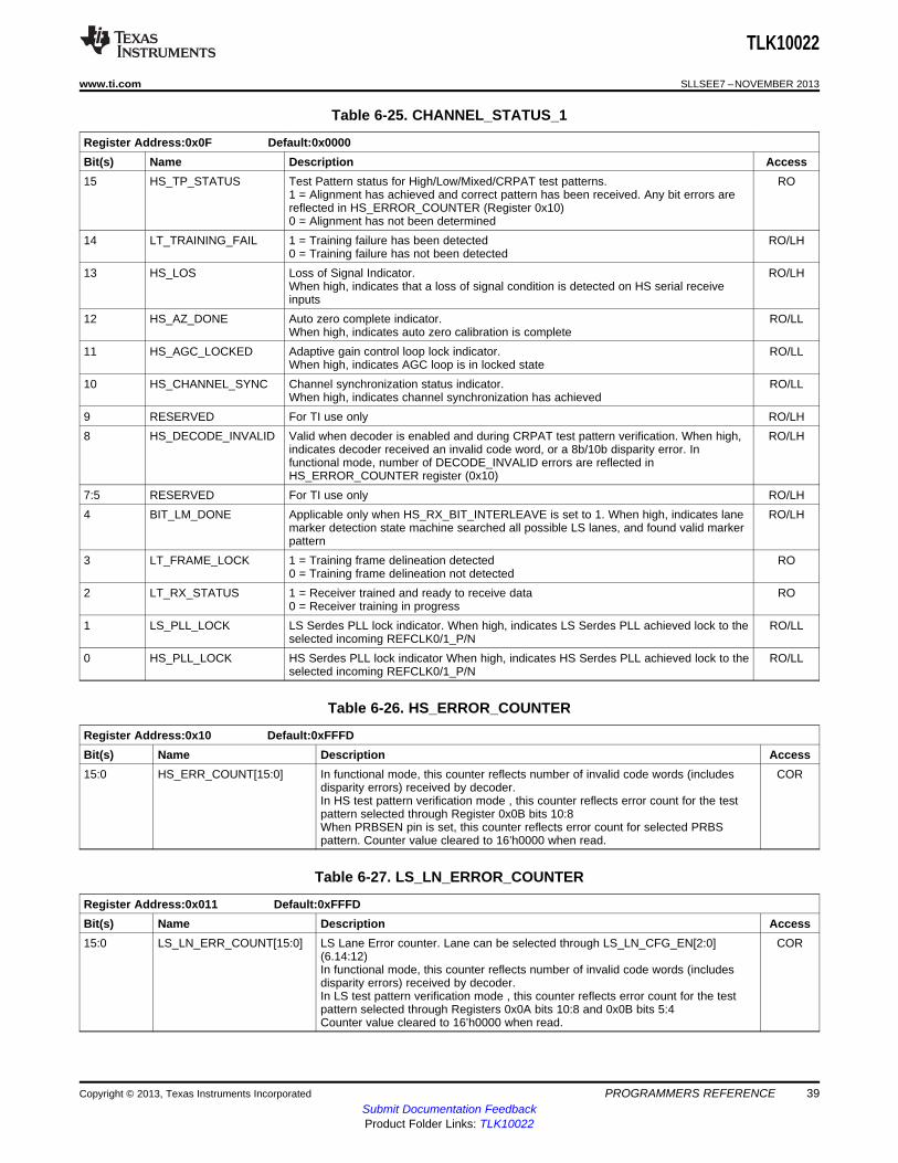
TLK10022
www.ti.com SLLSEE7 –NOVEMBER 2013
Table 6-25. CHANNEL_STATUS_1
Register Address:0x0F SPACER Default:0x0000Bit(s) Name Description Access15 HS_TP_STATUS Test Pattern status for High/Low/Mixed/CRPAT test patterns. RO
1 = Alignment has achieved and correct pattern has been received. Any bit errors arereflected in HS_ERROR_COUNTER (Register 0x10)0 = Alignment has not been determined
14 LT_TRAINING_FAIL 1 = Training failure has been detected RO/LH0 = Training failure has not been detected
13 HS_LOS Loss of Signal Indicator. RO/LHWhen high, indicates that a loss of signal condition is detected on HS serial receiveinputs
12 HS_AZ_DONE Auto zero complete indicator. RO/LLWhen high, indicates auto zero calibration is complete
11 HS_AGC_LOCKED Adaptive gain control loop lock indicator. RO/LLWhen high, indicates AGC loop is in locked state
10 HS_CHANNEL_SYNC Channel synchronization status indicator. RO/LLWhen high, indicates channel synchronization has achieved
9 RESERVED For TI use only RO/LH8 HS_DECODE_INVALID Valid when decoder is enabled and during CRPAT test pattern verification. When high, RO/LH
indicates decoder received an invalid code word, or a 8b/10b disparity error. Infunctional mode, number of DECODE_INVALID errors are reflected inHS_ERROR_COUNTER register (0x10)
7:5 RESERVED For TI use only RO/LH4 BIT_LM_DONE Applicable only when HS_RX_BIT_INTERLEAVE is set to 1. When high, indicates lane RO/LH
marker detection state machine searched all possible LS lanes, and found valid markerpattern
3 LT_FRAME_LOCK 1 = Training frame delineation detected RO0 = Training frame delineation not detected
2 LT_RX_STATUS 1 = Receiver trained and ready to receive data RO0 = Receiver training in progress
1 LS_PLL_LOCK LS Serdes PLL lock indicator. When high, indicates LS Serdes PLL achieved lock to the RO/LLselected incoming REFCLK0/1_P/N
0 HS_PLL_LOCK HS Serdes PLL lock indicator When high, indicates HS Serdes PLL achieved lock to the RO/LLselected incoming REFCLK0/1_P/N
Table 6-26. HS_ERROR_COUNTER
Register Address:0x10 SPACER Default:0xFFFDBit(s) Name Description Access15:0 HS_ERR_COUNT[15:0] In functional mode, this counter reflects number of invalid code words (includes COR
disparity errors) received by decoder.In HS test pattern verification mode , this counter reflects error count for the testpattern selected through Register 0x0B bits 10:8When PRBSEN pin is set, this counter reflects error count for selected PRBSpattern. Counter value cleared to 16’h0000 when read.
Table 6-27. LS_LN_ERROR_COUNTER
Register Address:0x011 SPACER Default:0xFFFDBit(s) Name Description Access15:0 LS_LN_ERR_COUNT[15:0] LS Lane Error counter. Lane can be selected through LS_LN_CFG_EN[2:0] COR
(6.14:12)In functional mode, this counter reflects number of invalid code words (includesdisparity errors) received by decoder.In LS test pattern verification mode , this counter reflects error count for the testpattern selected through Registers 0x0A bits 10:8 and 0x0B bits 5:4Counter value cleared to 16’h0000 when read.
Copyright © 2013, Texas Instruments Incorporated PROGRAMMERS REFERENCE 39Submit Documentation FeedbackProduct Folder Links: TLK10022

TLK10022
SLLSEE7 –NOVEMBER 2013 www.ti.com
Table 6-28. LS_STATUS_1 (1)
Register Address:0x013 SPACERDefault:0x0000Bit(s) Name Description Access15 LS_TP_STATUS Test Pattern status for LS High/Low/Mixed/CRPAT test patterns. RO
1 = Alignment has achieved and correct pattern has been received. Any bit errorsare reflected in LS_LN_ERROR_COUNTER register0 = Alignment has not been determined
14 LS_RXLOS_DETECT When high, indicates LOS state machine successfully detected valid LOS pattern ROfor the selected lane. This bit is the raw status of LS_ RXLOS_DETECT_LH.
13:12 RESERVED For TI use only. RO11 LS_INVALID_DECODE LS Invalid decode error for selected lane. Error count for each lane can also be RO/LH
monitored through respective LS_LN_ERROR_COUNTER registers10 LS_LOS Loss of Signal Indicator. RO/LH
When high, indicates that a loss of signal condition is detected on LS serial receiveinputs for selected lane.
9 LS_RXLOS_DETECT_LH When high, indicates LOS state machine successfully detected valid LOS pattern RO/LHfor the selected lane.
8 LS_CH_SYNC_STATUS LS Channel sync status for selected lane. RO/LL7:4 RESERVED For TI use only. RO3 LS_TX_FIFO_UNDERFLOW When high, indicates underflow has occurred in the transmit datapath lane (CTC) RO/LH
FIFO.2 LS_TX_FIFO_OVERFLOW When high, indicates overflow has occurred in the transmit datapath lane (CTC) RO/LH
FIFO.1 LS_RX_FIFO_UNDERFLOW When high, indicates underflow has occurred in the receive datapath lane (CTC) RO/LH
FIFO.0 LS_RX_FIFO_OVERFLOW When high, indicates overflow has occurred in the receive datapath lane (CTC) RO/LH
FIFO.
(1) This is per lane status register. Lane can be selected through LS_LN_CFG[14:12] (Register 0x06)
Table 6-29. HS_STATUS_1
Register Address:0x014 SPACER Default:0x0000Bit(s) Name Description Access15:12 RESERVED For TI use only. RO/LH11 RX1_LANE_ALIGN RX1 lane align status on receive path10 RX0_LANE_ALIGN RX0 lane align status on receive path9 TX1_LANE_ALIGN TX1 lane align status on transmit path8 TX0_LANE_ALIGN TX0 lane align status on transmit path7:4 RESERVED For TI use only. RO3 HS_RX1_FIFO_UNDERFLOW When high, indicates underflow has occurred in the receive datapath lane FIFO RO/LH
when alternate channel HS Rx data is selected.2 HS_RX1_FIFO_OVERFLOW When high, indicates overflow has occurred in the receive datapath lane FIFO
when alternate channel HS Rx data is selected .1 HS_RX0_FIFO_UNDERFLOW When high, indicates underflow has occurred in the receive datapath lane FIFO.0 HS_RX0_FIFO_OVERFLOW When high, indicates overflow has occurred in the receive datapath lane FIFO.
40 PROGRAMMERS REFERENCE Copyright © 2013, Texas Instruments IncorporatedSubmit Documentation FeedbackProduct Folder Links: TLK10022

TLK10022
www.ti.com SLLSEE7 –NOVEMBER 2013
Table 6-30. CLK_CONTROL
Register Address:0x15 SPACER Default: 0x0280Bit(s) Name Description Access15:10 RESERVED For TI use only. Always reads 0. RW9 CLKOUT_EN Output clock enable. 0 = Holds CLKOUTx_P/N output to a fixed value. RW
1 = Allows CLKOUTx_P/N output to toggle normally (Default 1’b1)8 CLKOUT_POWERDOWN 0 = Normal operation (Default 1’b0) RW
1 = Enable CLKOUTx_P/N Power Down.7:4 CLKOUT_DIV[3:0] Output clock divide setting. This value is used to divide selected clock (Selected RW
using CLKOUT_SEL) before giving it out onto respective channel CLKOUTx_P/N.0000 = Divide by 10001 = RESERVED0010 = RESERVED0011 = RESERVED0100 = Divide by 20101 = RESERVED0110 = RESERVED0111 = RESERVED1000 = Divide by 4 (Default 4’b1000)1001 = Divide by 8 1010 = Divide by 161011 = RESERVED1100 = Divide by 51101 = Divide by 101110 = Divide by 201111 = Divide by 25
3:0 CLKOUT_SEL[3:0] Output clock select. Selected Recovered clock sent out on CLKOUTxP/N pins RW(Default 4’b0000)00x0 = Selects Ch A HS recovered byte clock as output clock00x1 = Selects Ch A HS transmit byte clock as output clock010x = Selects Ch A HSRX VCO divide by 4 clock as output clock0110 = Selects Ch A LS recovered byte clock as output clock0111 = Selects Ch A LS transmit byte clock as output clock10x0 = Selects Ch B HS recovered byte clock as output clock10x1 = Selects Ch B HS transmit byte clock as output clock= Selects Ch B HSRX VCO divide by 4 clock as output clock1110 = Selects Ch B LS recovered byte clock as output clock1111 = Selects Ch B LS transmit byte clock as output clock
Table 6-31. SKEW_CONFIG_CONTROL
Register Address:0x16 SPACER Default:0x0000Bit(s) Name Description Access15:8 RESERVED For TI use only (Default 7’b0000000) RW6:4 RX0_SKEW_CONFIG[2:0] Skew config for lanes 0-3 on receive path (Default 3’b000) RW
000 - No Skew001 - Align lanes 0,1010 - Align lanes 0,1,2X11- Align lanes 0,1,2,3100 - Align lanes 2,3101 - Align lanes 0,1 and 2,3110 - Reserved
3 RESERVED For TI use only. Always reads 0. RW2:0 TX0_SKEW_CONFIG[2:0] Skew config for lanes 0-3 on transmit path (Default 3’b000) RW
000 - No Skew001 - Align lanes 0,1010 - Align lanes 0,1,2X11- Align lanes 0,1,2,3100 - Align lanes 2,3101 - Align lanes 0,1 and 2,3110 - Reserved
Copyright © 2013, Texas Instruments Incorporated PROGRAMMERS REFERENCE 41Submit Documentation FeedbackProduct Folder Links: TLK10022

TLK10022
SLLSEE7 –NOVEMBER 2013 www.ti.com
Table 6-32. HS_ALIGN_CODE_CONTROL
Register Address:0x17 SPACER Default:0x02BCBit(s) Name Description Access15 RESERVED For TI use only (Default 1’b0) RW14:12 TX_LANE_MARKER[2:0] Marker selection on transmit side (Default 3’b000) RW11 BIT_LM_EN 0 = Normal operation (Default 1’b0) RW
1 = Enable lane marker generation in selected LS TX lane throughTX_LANE_MARKERWhen set to 1, lane marker message is generated (CRC field set to32’hFE00_00FE).When LS_LM_EN and LS_LOS_EN are set to 1, lane marker message isgenerated.
10:0 RESERVED For TI use only (Default 11’h2BC) RW
Table 6-33. BIT_LM_CONTROL
Register Address:0x18SPACER Default:0x0CC8Bit(s) Name Description Access15 RESERVED For TI use only (Default 1’b0) RW14:12 RX_LANE_MARKER[2:0] Marker selection on receive side (Default 3’b000) RW11 BIT_LM_PATT_DETECT_EN Applicable only when RX_BIT_INTERLEAVE is set to 1. RW
0 = Normal operation1 = Enable marker detection (Default 1’b1)
10:0 RESERVED For TI use only (Default 11’h4C8) RW
Table 6-34. LS_TXFIFO_CONTROL
Register Address:0x19 SPACER Default:0x02BCBit(s) Name Description Access15:13 LS_TXFIFO_DEPTH_SEL[2:0] TX FIFO depth select (Default 3’b000) RW12:11 LS_TXFFIO_WMK_SEL[1:0] TX FIFO Water mark select (Default 2’b00) RW10 LS_CHSYNC_ALIGN_CODE_EN Lane can be selected in LS_SERDES_CONTROL_1. RW
0 = Normal operation (Default 1’b0)1 = Use align code specified in LS_CH_SYNC_ALIGN_CODE in LS ch syncSM
9:0 LS_CHSYNC_ALIGN_CODE[9:0] Lane can be selected in LS_SERDES_CONTROL_1. RW10 bit align code to use when LS_CHSYNC_ALIGN_CODE_EN is set(Default 10’h2BC)
Table 6-35. LN_DATA_SRC_CONTROL
Register Address:0x1B SPACER Default:0x3020 (1)
Bit(s) Name Description Access15:14 LN_RX_DIV_RATE[1:0] Divided rate control on the receive side (Default 2’b00) RW
LS divided rate selection on receive path. Settings are applicable for the lanesselected through LS_LN_CFG_EN[3:0] (6.15:14)
13 LN_RX_CTC_EN LS CTC control on receive path. Settings are applicable for the lanes selected RWthrough LS_LN_CFG_EN[3:0] (6.15:14)0 = CTC disabled for the selected lane on receive path1 = CTC enabled for the selected lane on receive path (Default 1’b1)
12:11 LN_RX_DATA_SRC_SEL[1:0] Lane data source selection. Selects the data for selected lane that will be sent out on RWLS receive out. Settings are applicable for the lanes selected throughLS_LN_CFG_EN[3:0] (6.15:14)00 = LS input of same channel01 = LS input of alternate channel10 = HS input of same channel (Default 2’b10)11 = HS input of alternate channel
(1) Default for ln0 is 0x3020, ln1 is 0x3121, ln2 is 0x3222, ln 3 is 0x3323
42 PROGRAMMERS REFERENCE Copyright © 2013, Texas Instruments IncorporatedSubmit Documentation FeedbackProduct Folder Links: TLK10022

TLK10022
www.ti.com SLLSEE7 –NOVEMBER 2013
Table 6-35. LN_DATA_SRC_CONTROL (continued)Register Address:0x1B SPACER Default:0x3020 (1)
Bit(s) Name Description Access10:8 LN_RX_DATA_LANE_SEL[2:0] Lane selection for the data source selected through LN_RX_DATA_SRC_SEL. RW
Selects the data for selected lane that will be sent out on LS receive out. Settingsare applicable for the lanes selected through LS_LN_CFG_EN[3:0] (6.15:14)x00 = Lane 0 input (Default 3’b000)x01 = Lane 1 inputx10 = Lane 2 inputx11 = Lane 3 input
7:6 LN_TX_DIV_RATE[1:0] Divided rate control on the receive side (Default 2’b00) RWLS divided rate selection on transmit path. Settings are applicable for the lanesselected through LS_LN_CFG_EN[3:0] (6.15:14)
5 LN_TX_CTC_EN LS CTC control on transmit path. Settings are applicable for the lanes selected RWthrough LS_LN_CFG_EN[3:0] (6.15:14)0 = CTC disabled for the selected lane on transmit path1 = CTC enabled for the selected lane on transmit path (Default 1’b0)
4:3 LN_TX_DATA_SRC_SEL[4:3] LS lane data source selection. Selects the data for selected lane that will be sent out RWon HS transmit out. Settings are applicable for the lanes selected throughLS_LN_CFG_EN[3:0] (6.15:14)0x = LS input10 = HS input (Default 2’b10)11 = HS input of alternate macro
2:0 LN_TX_DATA_SRC_SEL[2:0] Lane selection for the data source selected through LN_TX_DATA_SRC_SEL[4:3]. RWSelects the data for selected lane that will be sent out on HS transmit out. Settingsare applicable for the lanes selected through LS_LN_CFG_EN[3:0] (6.15:14)x00 = Lane 0 input (Default 3’b000)x01 = Lane 1 inputx10 = Lane 2 inputx11 = Lane 3 input
Table 6-36. LS_CH_CONTROL_1
Register Address:0x1C SPACER Default: 0x0000Bit(s) Name Description Access15 RESERVED For TI use only (Default 1’b0) RW/SC14:12 LS_RXFIFO_DEPTH_SEL[2:0] RX FIFO depth select (Default 3’b000) RW11:10 LS_RXFIFO_WMK_SEL[1:0] RX FIFO Water mark select (Default 2’b00) RW9 RX_GIGE_EN 0 = Disable GIGE mode on receive path (Default 1’b0) RW
1 = Enable GIGE mode on receive path8 TX_GIGE_EN 0 = Disable GIGE mode on transmit path (Default 1’b0) RW
1 = Enable GIGE mode on transmit path7:6 RESERVED For TI use only (Default 2’b00) RW5 LS_CHSYNC_FORCE_SYNC Lane can be selected in LS_SERDES_CONTROL_1. RW
0 = Keep byte alignment determined by ch sync state machine (Default 1’b0)1 = Force byte alignment to 9 unless LS_CHSYNC_JOG_EN is 1
4 RESERVED For TI use only (Default 1'b0) RW3 LS_ENC_BYPASS 1 = Disables Encoder on LS side on selected lane. RW
0 = Normal operation (1’b0)2 LS_DEC_BYPASS 1 = Disables Decoder on LS side on selected lane. RW
0 = Normal operation (1’b0)1:0 LS_CH_SYNC_HYS_SEL[1:0] LS Channel synchronization hysteresis selection for selected lane. Lane can be RW
selected in LS_SERDES_CONTROL_1.00 = The channel synchronization, when in the synchronization state, performs theEthernet standard specified hysteresis to return to the LOS state (Default 2’b00)01 = A single 8b/10b invalid decode error or disparity error causes the channelsynchronization state machine to immediately transition from sync to LOS10 = Two adjacent 8b/10b invalid decode errors or disparity errors cause thechannel synchronization state machine to immediately transition from sync to LOS11 = Three adjacent 8b/10b invalid decode errors or disparity errors cause thechannel synchronization state machine to immediately transition from sync to LOS
Copyright © 2013, Texas Instruments Incorporated PROGRAMMERS REFERENCE 43Submit Documentation FeedbackProduct Folder Links: TLK10022

TLK10022
SLLSEE7 –NOVEMBER 2013 www.ti.com
Table 6-37. HS_CH_CONTROL_1
Register Address:0x1D SPACER Default: 0x0880Bit(s) Name Description Access15 RESERVED For TI use only (Default 1’b0) RW/SC14:12 HS_RXFIFO_DEPTH_SEL[2:0] FIFO depth select for both HS RX0/RX1 FIFO’s (Default 3’b000) RW11 RX_LANE_MARKER_EN Marker enable control on receive side (Default 1’b1) RW
0 = Normal operation1 = Enable marker search/replacement. Marker search/replacement charactercan be selected in VS_RX_MARKER_SEARCH_CHARACTER (0x8002.9:0),VS_RX_MARKER_REPLACE_CHARACTER (0x8003.9:0)
10:8 RESERVED For TI use only (Default 3’b000) RW7 TX_LANE_MARKER_EN Marker enable control on transmit side (Default 1’b1) RW
0 = Normal operation1 = Enable marker search/replacement. Marker search/replacement charactercan be selected in VS_TX_MARKER_SEARCH_CHARACTER (0x8000.9:0),VS_TX_MARKER_REPLACE_CHARACTER (0x8001.9:0)
6 RESERVED For TI use only (Default 1’b0) RW5 HS_CHSYNC_FORCE_SYNC 0 = Keep byte alignment determined by ch sync state machine (Default 1’b0) RW
1 = Force byte alignment to 9 unless HS_CHSYNC_JOG_EN is 14 HS_CHSYNC_JOG_EN 0 = Disable manual jog function (Default 1’b0) RW
1 = Enable manual jog function3 HS_ENC_BYPASS 0 = Normal operation. (Default 1’b0) RW
1 = Disables 8B/10B encoder on HS side.2 HS_DEC_BYPASS 0 = Normal operation. (Default 1’b0) RW
1 = Disables 8B/10B decoder on HS side.1:0 HS_CH_SYNC_HYSTERESIS[1:0] Channel synchronization hysteresis control on the HS receive channel. RW
00 = The channel synchronization, when in the synchronization state, performsthe Ethernet standard specified hysteresis to return to the unsynchronizedstate (Default 2’b00)01 = A single 8b/10b invalid decode error or disparity error causes the channelsynchronization state machine to immediately transition from sync to unsync10 = Two adjacent 8b/10b invalid decode errors or disparity errors cause thechannel synchronization state machine to immediately transition from sync tounsync11 = Three adjacent 8b/10b invalid decode errors or disparity errors cause thechannel synchronization state machine to immediately transition from sync tounsync
Table 6-38. EXT_ADDRESS_CONTROL
Register Address:0x1E SPACER Default: 0x0000Bit(s) Name Description Access15:0 EXT_ADDR_CONTROL[15:0] This register should be written with the extended register address to be RW
written/read. Contents of address written in this register can be accessed from Reg0x1F (Default 16’h0000)
Table 6-39. EXT_ADDRESS_DATA
Register Address:0x1F SPACER Default: 0x0000Bit(s) Name Description Access15:0 EXT_ADDR_DATA[15:0] This register contains the data associated with the register address written in RW
Register 0x1E (Default 16’h0000)
Table 6-40. VS_TX_MARKER_SEARCH_CHAR
Register Address:0x8000 SPACER Default: 0x02BCBit(s) Name Description Access9:0 TX_SEARCH_MARKER[9:0] TX Search marker character (Default 10’h2BC)
44 PROGRAMMERS REFERENCE Copyright © 2013, Texas Instruments IncorporatedSubmit Documentation FeedbackProduct Folder Links: TLK10022

TLK10022
www.ti.com SLLSEE7 –NOVEMBER 2013
Table 6-41. VS_TX_MARKER_REPLACE_CHAR
Register Address:0x8001 SPACER Default: 0x027CBit(s) Name Description Access9:0 TX_REPLACE_MARKER[9:0] TX Replace marker character (Default 10’h27C)
Table 6-42. VS_RX_MARKER_SEARCH_CHAR
Register Address:0x8002 SPACER Default: 0x027CBit(s) Name Description Access9:0 RX_SEARCH_MARKER[9:0] RX Search marker character (Default 10’h27C) RW
Table 6-43. VS_RX_MARKER_REPLACE_CHAR
Register Address:0x8003 SPACER Default: 0x02BCBit(s) Name Description Access9:0 RX_REPLACE_MARKER[9:0] RX Replace marker character (Default 10’h2BC) RW
Table 6-44. VS_TX_IDLE_P_CHAR
Register Address:0x8004 SPACER Default: 0x02BCBit(s) Name Description Access9:0 TX_IDLE_P[9:0] TX Idle P character (Default 10’h2BC) RW
Table 6-45. VS_TX_IDLE_N_CHAR
Register Address:0x8005 SPACER Default: 0x02BCBit(s) Name Description Access9:0 TX_IDLE_N[9:0] TX Idle N character (Default 10’h2BC) RW
Table 6-46. VS_RX_IDLE_P_CHAR
Register Address:0x8006 SPACER Default: 0x02BCBit(s) Name Description Access9:0 RX_IDLE_P[9:0] RX Idle P character (Default 10’h2BC) RW
Table 6-47. VS_RX_IDLE_N_CHAR
Register Address:0x8007 SPACER Default: 0x02BCBit(s) Name Description Access9:0 RX_IDLE_N[9:0] RX Idle N character (Default 10’h2BC) RW
Table 6-48. VS_TX_SCR_CONTROL
Register Address:0x8009 SPACER Default: 0xFC00Bit(s) Name Description Access15:2 RESERVED For TI use only (Default 14'b11111100000000) RW1 TX_SCR_20_EN 1 = Enable 20 bit scrambler (post-encoder) on transmit side(Default 1’b0) RW
0 = Disable 20 bit scrambler (post-encoder) on transmit side0 TX_SCR_16_EN 1 = Enable 16 bit scrambler (pre-encoder) on transmit side. Seed can be set RW
through 0x800C and 0x800D (Default 1’b0)0 = Disable 16 bit scrambler (pre-encoder) on transmit side
Copyright © 2013, Texas Instruments Incorporated PROGRAMMERS REFERENCE 45Submit Documentation FeedbackProduct Folder Links: TLK10022

TLK10022
SLLSEE7 –NOVEMBER 2013 www.ti.com
Table 6-49. VS_TX_SCR_SEED_CONTROL_1
Register Address:0x800C SPACER Default: 0x0000Bit(s) Name Description Access15:0 TX_SCR_SEED[31:16] [31:16] bits of 32 bit Tx scrambler seed. TX_SCR_SEED[31:0] must be set to a RW
non-zero value for scrambler to work properly (Default 16’h0000).
Table 6-50. VS_TX_SCR_SEED_CONTROL_0
Register Address:0x800D SPACER Default: 0x01FCBit(s) Name Description Access15:0 TX_SCR_SEED[15:0] [15:0] bits of 32 bit Tx scrambler seed. Bit 0 always set to 1’b0. RW
TX_SCR_SEED[31:0] must be set to a non-zero value for scrambler to workproperly (Default 16’h01FC).
Table 6-51. VS_TX_SCR_POLY_CONTROL_1
Register Address:0x800E SPACER Default: 0x0000Bit(s) Name Description Access15:0 TX_SCR_POLY[31:16] [31:16] bits of 32 bit Tx scrambler polynomial (Default 16’h0000). RW
Table 6-52. VS_TX_SCR_POLY_CONTROL_0
Register Address:0x800F SPACER Default: 0x00C0Bit(s) Name Description Access15:0 TX_SCR_POLY[15:0] [15:0] bits of 32 bit Tx scrambler polynomial. Bit 0 always set to 1’b0. (Default RW
16’h00C0).
Table 6-53. VS_RX_DESCR_CONTROL
Register Address:0x8019 SPACER Default: 0xFC00Bit(s) Name Description Access15:2 RESERVED For TI use only (Default 14'b11111100000000) RW1 RX_DESCR_20_EN 1 = Enable 20 bit descrambler (pre-decoder) on receive side(Default 1’b0) RW
0 = Disable 20 bit descrambler (pre-decoder) on receive side0 RX_DESCR_16_EN 1 = Enable 16 bit descrambler (post-decoder) on receive side. Seed can be set RW
through 0x801C and 0x801D (Default 1’b0)0 = Disable 16 bit descrambler (post-decoder) on receive side
Table 6-54. VS_RX_DESCR_SEED_CONTROL_1
Register Address:0x801C SPACER Default: 0x0000Bit(s) Name Description Access15:0 RX_DESCR_SEED[31:16] [31:16] bits of 32 bit Rx descrambler seed. RX_DESCR_SEED[31:0] must be set to RW
a non-zero value for descrambler to work properly (Default 16’h0000).
Table 6-55. VS_RX_DESCR_SEED_CONTROL_0
Register Address:0x801D SPACER Default: 0x01FCBit(s) Name Description Access15:0 RX_DESCR_SEED[15:0] [15:0] bits of 32 bit Rx descrambler seed. Bit 0 always set to 1’b0. RW
RX_DESCR_SEED[31:0] must be set to a non-zero value for descrambler to workproperly (Default 16’h01FC).
46 PROGRAMMERS REFERENCE Copyright © 2013, Texas Instruments IncorporatedSubmit Documentation FeedbackProduct Folder Links: TLK10022

TLK10022
www.ti.com SLLSEE7 –NOVEMBER 2013
Table 6-56. VS_RX_DESCR_POLY_CONTROL_1
Register Address:0x801E SPACER Default: 0x0000Bit(s) Name Description Access15:0 RX_DESCR_POLY[31:16] [31:16] bits of 32 bit Rx descrambler polynomial (Default 16’h0000). RW
Table 6-57. VS_RX_DESCR_POLY_CONTROL_0
Register Address:0x801F SPACER Default: 0x00C0Bit(s) Name Description Access15:0 RX_DESCR_POLY[15:0] [15:0] bits of 32 bit Rx descrambler polynomial. Bit 0 always set to 1’b0. (Default RW
16’h00C0).
Table 6-58. MC_AUTO_CONTROL
Register Address:0x8021 SPACER Default: 0x000ABit(s) Name Description Access15:7 RESERVED For TI use only (Default 9'b000000000) RW6 HS_PLL_LOCK_CHECK_DISABLE 1 = Disable auto HS pll lock status check. RW
0 = Enable auto HS pll lock status check (Default 1’b0)5 HS_LOS_CHECK_DISABLE 1 = Disable auto HS los status check RW
0 = Enable auto HS los sync status check (Default 1’b0)4 SYNC_STATUS_CHECK_DISABLE 1 = Disable auto sync status check. RW
0 = Enable auto sync status check. (Default 1’b0)3 CLKOUT_EN_AUTO_DISABLE This bit controls the signal which flat lines CLKOUT and applicable only RW
when CLKOUT is selected to have HS Recovered byte clock1 = CLKOUT clock flat lined if HS LOS is detected (Default 1’b1)0 = CLKOUT clock not flat lined if HS LOS is detected
2:0 RESERVED For TI use only (Default 3’b111) RW
Table 6-59. VS_LS_TX_ERROR_CODE
Register Address:0x8026 SPACER Default: 0x02FEBit(s) Name Description Access9:0 LS_TX_ERROR_CODE[9:0] Error code to be transmitted if LS TX FIFO has error (Default 10’h2FE) RW
Table 6-60. VS_LS_RX_ERROR_CODE
Register Address:0x8027 SPACER Default: 0x02FEBit(s) Name Description Access9:0 LS_RX_ERROR_CODE[9:0] Error code to be transmitted if LS RX FIFO has error (Default 10’h2FE) RW
Table 6-61. VS_HS_RX_ERROR_CODE
Register Address:0x8028SPACER Default: 0x02FEBit(s) Name Description Access9:0 HS_RX_ERROR_CODE[9:0] Error code to be transmitted if HS RX FIFO has error (Default 10’h2FE) RW
Table 6-62. TI_RESERVED_STATUS
Register Address:0x9020 SPACER Default: 0x0000Bit(s) Name Description Access15:1 RESERVED For TI use only. RO0 LT_START_PROTOCOL 1 = Start up protocol in progress RO
0 = Start up protocol complete
Copyright © 2013, Texas Instruments Incorporated PROGRAMMERS REFERENCE 47Submit Documentation FeedbackProduct Folder Links: TLK10022

TLK10022
SLLSEE7 –NOVEMBER 2013 www.ti.com
Table 6-63. LT_LINK_PARTNER_CONTROL
Register Address: 0x9098 SPACER Default: 0x0000Bit(s) Name Description Access13 LT_LP_PRESET 1 = KR preset coefficients RO
0 = Normal operation12 LT_LP_INITIALIZE 1 = Initialize KR coefficients RO
0 = Normal operation9:8 LT_LP_COEFF_SWG Swing update RO
11 = Reserved01 = Increment10 = Decrement00 = Hold
7:6 LT_LP_COEFF_PS2 Post2 tap control update RO11 = Reserved01 = Increment10 = Decrement00 = Hold
5:4 LT_LP_COEFF_P1 Coefficient K(+1) update RO11 = Reserved01 = Increment10 = Decrement00 = Hold
3:2 LT_LP_COEFF_0 Coefficient K(0) update RO11 = Reserved01 = Increment10 = Decrement00 = Hold
1:0 LT_LP_COEFF_M1 Coefficient K(-1) update RO11 = Reserved01 = Increment10 = Decrement00 = Hold (Default 2’b00)
48 PROGRAMMERS REFERENCE Copyright © 2013, Texas Instruments IncorporatedSubmit Documentation FeedbackProduct Folder Links: TLK10022

TLK10022
www.ti.com SLLSEE7 –NOVEMBER 2013
Table 6-64. LT_LINK_PARTNER_STATUS
Register Address: 0x9099 SPACER Default: 0x0000Bit(s) Name Description Access15 LT_LP_RX_READY 1 = LP receiver has determined that training is complete and prepared to RO
receive data0 = LP receiver is requesting that training continue
9:8 LT_LP_COEFF_SWG_STAT Swing update RO11 = Maximum01 = Updated10 = Minimum00 = Not updated
7:6 LT_LP_COEFF_PS2_STAT Post2 tap control update RO11 = Maximum01 = Updated10 = Minimum00 = Not updated
5:4 LT_LP_COEFF_P1_STAT Plus 1 update RO11 = Maximum01 = Updated10 = Minimum00 = Not updated
3:2 LT_LP_COEFF_0_STAT 0 update RO11 = Maximum01 = Updated10 = Minimum00 = Not updated
1:0 LT_LP_COEFF_M1_STAT Minus 1 update RO11 = Maximum01 = Updated10 = Minimum00 = Not updated
Copyright © 2013, Texas Instruments Incorporated PROGRAMMERS REFERENCE 49Submit Documentation FeedbackProduct Folder Links: TLK10022

TLK10022
SLLSEE7 –NOVEMBER 2013 www.ti.com
Table 6-65. LT_LOCAL_DEVICE_CONTROL (1) (2) (3)
Register Address: 0x909A SPACER Default: 0x0000Bit(s) Name Description Access15:14 RESERVED For TI use only RO13 LT_LD_PRESET 1 = KR preset coefficients RO
0 = Normal operation (Default 1’b0)1 = Initialize KR coefficients12 LT_ LD_INITIALIZE RO0 = Normal operation (Default 1’b0)
9:8 LT_LD_COEFF_SWG Swing update RO11 = Reserved01 = Increment10 = Decrement00 = Hold (Default 2’b00)
7:6 LT_LD_COEFF_PS2 Post2 tap control update RO11 = Reserved01 = Increment10 = Decrement00 = Hold (Default 2’b00)
5:4 LT_ LD_COEFF_P1 Coefficient K(+1) update RO11 = Reserved01 = Increment10 = Decrement00 = Hold (Default 2’b00)
3:2 LT_ LD_COEFF_0 Coefficient K(0) update RO11 = Reserved01 = Increment10 = Decrement00 = Hold (Default 2’b00)
1:0 LT_ LD_COEFF_M1 Coefficient K(-1) update RO11 = Reserved01 = Increment10 = Decrement00 = Hold (Default 2’b00)
(1) This register values reflects muxed version of the controls coming from search algorithm(2) These bits are RW during manual search mode(3) These bits are RW during manual search mode
Table 6-66. LT_LOCAL_DEVICE_STATUS
Register Address: 0x909B SPACER Default: 0x0000Bit(s) Name Description Access15 LT_ LD_RX_READY 1 = LD receiver has determined that training is complete and prepared to RO
receive data0 = LD receiver is requesting that training continue
5:4 LT_ LD_COEFF_P1_STAT Plus 1 update RO11 = Maximum01 = Updated10 = Minimum00 = Not updated
3:2 LT_ LD_COEFF_0_STAT 0 update RO11 = Maximum01 = Updated10 = Minimum00 = Not updated
1:0 LT_ LD_COEFF_M1_STAT Minus 1 update RO11 = Maximum01 = Updated10 = Minimum00 = Not updated
50 PROGRAMMERS REFERENCE Copyright © 2013, Texas Instruments IncorporatedSubmit Documentation FeedbackProduct Folder Links: TLK10022

TLK10022
www.ti.com SLLSEE7 –NOVEMBER 2013
Table 6-67. TI_Reserved Control and Status RegistersREGISTER DEFAULT REGISTER DEFAULTREGISTER NAME ACCESS REGISTER NAME ACCESSADDRESS VALUE ADDRESS VALUE
TI_RESERVED_CONTROL 0x0C 0xFFFF RW TI_RESERVED_CONTROL 0x9003 0xAF14 RW
TI_RESERVED_STATUS 0x12 0x0000 COR TI_RESERVED_CONTROL 0x9004 0x007F RW
TI_RESERVED_CONTROL 0x1A 0x03C8 RW TI_RESERVED_CONTROL 0x9005 0x1C00 RW
TI_RESERVED_CONTROL 0x8008 0x0115 RW TI_RESERVED_CONTROL 0x9006 0x0000 RW
TI_RESERVED_CONTROL 0x800A 0xBC3C RW TI_RESERVED_CONTROL 0x9007 0x4890 RW
TI_RESERVED_CONTROL 0x800B 0x0000 RW TI_RESERVED_CONTROL 0x9008 0xC00C RW
TI_RESERVED_CONTROL 0x801A 0xBC3C RW TI_RESERVED_CONTROL 0x9009 0xD333 RW
TI_RESERVED_CONTROL 0x8020 0x0200 RW TI_RESERVED_CONTROL 0x900A 0x5E8F RW
TI_RESERVED_CONTROL 0x8022 0x0000 RW TI_RESERVED_CONTROL 0x900B 0xAFAF RW
TI_RESERVED_CONTROL 0x8023 0x0190 RW TI_RESERVED_CONTROL 0x900C 0x0800 RW
TI_RESERVED_CONTROL 0x8024 0x0000 RW TI_RESERVED_CONTROL 0x900D 0x461A RW
TI_RESERVED_CONTROL 0x8025 0xF000 RW TI_RESERVED_CONTROL 0x900E 0x1723 RW
TI_RESERVED_CONTROL 0x8029 0x02FE RW TI_RESERVED_CONTROL 0x900F 0x7003 RW
0x8030 -TI_RESERVED_STATUS 0x0000 RO TI_RESERVED_CONTROL 0x9010 0x0851 RW0x8033
TI_RESERVED_STATUS 0x8035 0x0000 RO TI_RESERVED_CONTROL 0x9011 0x1EFF RW
TI_RESERVED_CONTROL 0x8050 0x0000 RW TI_RESERVED_STATUS 0x9021 0xFFFD COR
0x8060 -TI_RESERVED_STATUS 0xFFFD COR TI_RESERVED_STATUS 0x9022 0x0000 RO0x8067
0x8068 -TI_RESERVED_STATUS 0x0000 COR TI_RESERVED_STATUS 0x9023 0x0000 RO0x806F
0x8070 - 0x9024 -TI_RESERVED_STATUS 0xFFFD COR TI_RESERVED_STATUS 0x0000 RO0x8077 0x9029
0x8078 -TI_RESERVED_STATUS 0x0000 COR TI_RESERVED_CONTROL 0xA000 0x0000 RW0x807F
0xA010 -TI_RESERVED_CONTROL 0x8100 0x0000 RW TI_RESERVED_STATUS 0x0000 RO0xA018
TI_RESERVED_CONTROL 0x8102 0xF280 RW TI_RESERVED_CONTROL 0xA116 0x0000 RW
TI_RESERVED_CONTROL 0x8103 0x0000 RW TI_RESERVED_CONTROL 0xA117 0x0000 RW
TI_RESERVED_CONTROL 0x9000 0x0249 RW TI_RESERVED_STATUS 0xA118 0x0000 RO
TI_RESERVED_CONTROL 0x9001 0x0200 RW TI_RESERVED_STATUS 0xA119 0x0000 RO
Copyright © 2013, Texas Instruments Incorporated PROGRAMMERS REFERENCE 51Submit Documentation FeedbackProduct Folder Links: TLK10022

TLK10022
SLLSEE7 –NOVEMBER 2013 www.ti.com
7 ELECTRICAL CHARACTERISTICS
7.1 Absolute Maximum Ratingsover operating free-air temperature range (unless otherwise noted) (1) (2)
VALUEUNIT
MIN MAXDVDD, VDDA_LS/HS, VDDT_LS/HS, VPP, VDDD –0.3 1.4 V
Supply voltageVDDRA/B_LS/HS, VDDO[1:0] –0.3 2.2 V
Input voltage, VI, (LVCMOS/CML/Analog) –0.3 Supply + 0.3 VStorage temperature –65 150 °COperating junction temperature 105 °C
HBM 1 kVElectrostaticdischarge: CDM 500 VCharacterized free-air operating temperature range –40 85 °C
(1) Stresses beyond those listed under “absolute maximum ratings” may cause permanent damage to the device. These are stress ratingsonly and functional operation of the device at these or any other conditions beyond those indicated under “recommended operatingconditions” is not implied. Exposure to absolute-maximum-rated conditions for extended periods may affect device reliability.
(2) All voltages are with respect to ground (VSS).
7.2 Recommended Operating ConditionsPARAMETER TEST CONDITIONS MIN NOM MAX UNIT
Digital / analog supply VDDD, VDDA_LS/HS, DVDD, 0.95 1.00 1.05 Vvoltages VDDT_LS/HS, VPP1.5V nominal 1.425 1.5 1.575SERDES PLL regulator VDDRA_LS/HS, Vvoltage VDDRB_LS/HS 1.8V nominal 1.71 1.8 1.891.5V nominal 1.425 1.5 1.575LVCMOS I/O supply VDDO[1:0] Vvoltage 1.8V nominal 1.71 1.8 1.89
VDDD 580VDDA_LS/HS 600DVDD + VPP 650
IDD Supply current VDDT_LS/HS 10Gbps 600 mAVDDRA/B_LS 70VDDRA/B_HS 70VDDO[1:0] 10
Nominal 1.5Worst case supply voltage,temperature, and process atPD Power dissipation W10Gbps with both channels 1.9active, default swing andClkout settings.
VDDD 210VDDA 70DVDD + VPP 150
ISD Shutdown current PD* asserted mAVDDT 65VDDRA_HS/LS + 7VDDRB_HS/LSVDDO 5
TRISE REFCLK0P/N, REFCLK1P/N rise/fall time 10% to 90% 50 350 psJR REFCLK0P/N, REFCLK1P/N random Jitter 12kHz to 20MHz 1 ps
52 ELECTRICAL CHARACTERISTICS Copyright © 2013, Texas Instruments IncorporatedSubmit Documentation FeedbackProduct Folder Links: TLK10022

VCMT
0.5 *
VOD(pp)
bit
time
tr , tf
0.5 * VDE *
VOD(pp)
0.25 * VDE * VOD(pp)
0.25 * VOD(pp)
TLK10022
www.ti.com SLLSEE7 –NOVEMBER 2013
7.3 High Speed Side Serial Transmitter CharacteristicsPARAMETER TEST CONDITIONS MIN TYP MAX UNIT
SWING = 0000 50 130 220SWING = 0001 110 220 320SWING = 0010 180 300 430SWING = 0011 250 390 540SWING = 0100 320 480 650SWING = 0101 390 570 770SWING = 0110 460 660 880SWING = 0111 530 750 1000
TX output differential peak-to-peak voltageVOD(p-p) SWING = 1000 590 830 1100 mVppswingSWING = 1001 660 930 1220SWING = 1010 740 1020 1320SWING = 1011 820 1110 1430SWING = 1100 890 1180 1520SWING = 1101 970 1270 1610SWING = 1110 1060 1340 1680SWING = 1111 1090 1400 1740Transmitter disabled 30See register bits TWPOST1,TWPOST2, and –17.5/ +17.5/Vpre/post TX output pre/post cursor emphasis voltage TWPRE for de-emphasis settings. –37.5% +37.5%See Figure 7-2
VDDT –100-Ω differential termination, DC-VCMT TX output common mode voltage 0.25× mVcoupled VOD(p-p)
Differential output signal rise, fall timeTr, Tf 20% to 80%, 100Ω differential load 24 ps(20% to 80%), Differential load = 100ΩJT1 Serial output total jitter PLL Multiplier = 10 0.28 UIJD1 Serial output deterministic jitter PLL Multiplier = 10 0.15 UIJR1 Serial output random jitter PLL Multiplier = 10 0.15 UIDCD Duty cycle distortion PLL Multiplier = 10 0.035 UI
50 MHz < f < 2.5 GHz 9 dBSDD22 Differential output return loss
2.5 GHz < f < 7.5 GHz See (1) dB50 MHz < f < 2.5 GHz 6 dB
SCC22 Common-mode output return loss2.5 GHz < f < 7.5 GHz See (2) dB
T(LATENCY) Transmit path latency See Figure 3-5
(1) Differential input return loss, SDD22 = 9 – 12 log10(f / 2500MHz)) dB(2) Common-mode output return loss, SDD22 = 6 – 12 log10(f / 2500MHz)) dB
Figure 7-1. Transmit Output Waveform Parameter Definitions
Copyright © 2013, Texas Instruments Incorporated ELECTRICAL CHARACTERISTICS 53Submit Documentation FeedbackProduct Folder Links: TLK10022

0
-Vss
-Vpre
-V pst
-V 0/0
+V 0/0
+V pst
+Vpre
+Vss
UI
h -1 = TWPRE (0% -17 .5% for typical application) setting
h1 = TWPOST1 (0% -37.5% for typical application) setting
h0 = 1 - |h1| - |h -1 |
V0 /0 = Output Amplitude with TWPRE = 0%, TWPOST = 0%.
Vss = Steady State Output Voltage = V0/0 * | h1 + h0 + h- 1|
Vpre = PreCursor Output Voltage = V0 /0 * | -h1 – h0 + h -1|
Vpst = PostCursor Output Voltage = V0/0 * | - h1 + h0 + h- 1|
TLK10022
SLLSEE7 –NOVEMBER 2013 www.ti.com
Figure 7-2. Pre/Post Cursor Swing Definitions
54 ELECTRICAL CHARACTERISTICS Copyright © 2013, Texas Instruments IncorporatedSubmit Documentation FeedbackProduct Folder Links: TLK10022

0
5
10
15
20
25
30
35
40
1000 2000 3000 4000 5000 6000Frequency (MHz)
Fitt
ed A
ttenu
atio
n (d
B)
G001
TLK10022
www.ti.com SLLSEE7 –NOVEMBER 2013
7.4 High Speed Side Serial Receiver CharacteristicsPARAMETER TEST CONDITIONS MIN TYP MAX UNIT
Full rate, AC coupled 50 600VID RX input differential voltage, |RXP – RXN| mV
Half/Quarter/Eighth rate, AC coupled 50 800Full rate, AC coupled 100 1200RX input differential peak-to-peak voltageVID(pp) mVppswing, 2×|RXP – RXN| Half/Quarter/Eighth rate, AC coupled 100 1600
CI RX input capacitance 2 pFApplied sinusoidal jitter 0.115Applied random jitter 0.130Jitter tolerance, PRBS 31 test pattern at 10JTOL mVRMSGbps (See Figure 7-3 for attenuation curve) Applied duty cycle distortion 0.035Broadband noise amplitude (RMS) 5.2100 MHz < f < 0.75 × [Serial Bit Rate] 9
SDD11 Differential input return loss dB0.75 × [Serial Bit Rate] < f< [Serial Bit See (1)Rate]
t(LATENCY) Receive path latency See Figure 3-5
(1) Differential input return loss, SDD11 = 8 – 16.6 log10(f / (0.75 × [Serial Bit Rate])) dB
Figure 7-3. Fitted Channel Attenuation Limit
Copyright © 2013, Texas Instruments Incorporated ELECTRICAL CHARACTERISTICS 55Submit Documentation FeedbackProduct Folder Links: TLK10022

TLK10022
SLLSEE7 –NOVEMBER 2013 www.ti.com
7.5 Low Speed Side Serial Transmitter CharacteristicsPARAMETER TEST CONDITIONS MIN TYP MAX UNIT
SWING = 000 110 190 280SWING = 001 280 380 490SWING = 010 420 560 700SWING = 011 560 710 870Transmitter output differential peak-to-peakVOD(pp) mVppvoltage swing SWING = 100 690 850 1020SWING = 101 760 950 1150SWING = 110 800 1010 1230SWING = 111 830 1050 1270DE = 0000 0DE = 0001 0.42DE = 0010 0.87DE = 0011 1.34DE = 0100 1.83DE = 0101 2.36DE = 0110 2.92DE = 0111 3.52Transmitter output de-emphasis voltageDE dBswing reduction DE = 1000 4.16DE = 1001 4.86DE = 1010 5.61DE = 1011 6.44DE = 1100 7.35DE = 1101 8.38DE = 1110 9.54DE = 1111 10.87
VDDT – 0.5VCMT Transmitter output common mode voltage 100-Ω differential termination, DC-coupled × mV
VOD(p-p)
Differential output signal rise,tR, tF Fall time (20% to 80%) 30 ps
Differential Load = 100ΩJT Serial output total jitter 0.35 UIJD Serial output deterministic jitter 0.17 UIDCD Duty cycle distortion 0.035 UI
56 ELECTRICAL CHARACTERISTICS Copyright © 2013, Texas Instruments IncorporatedSubmit Documentation FeedbackProduct Folder Links: TLK10022

TLK10022
www.ti.com SLLSEE7 –NOVEMBER 2013
7.6 Low Speed Side Serial Receiver CharacteristicsPARAMETER TEST CONDITIONS MIN TYP MAX UNIT
Full rate, AC coupled 50 600Receiver input differential voltage,VID mV|INP – INN| Half/Quarter rate, AC coupled 50 800Full rate, AC coupled 100 1200Receiver input differential peak-to-peakVID(pp) mVdfppvoltage swing 2×|INP – INN| Half/Quarter rate, AC coupled 100 1600
CI Receiver input capacitance 2 pFZero crossing, Half/Quarter rate 0.66Jitter tolerance, total jitter at serial inputJTOL UIp-p(DJ + RJ) (BER 10-15) Zero crossing, Full rate 0.65Zero crossing, Half/Quarter rate 0.50
JDR Serial input deterministic jitter (BER 10-15) UIp-pZero crossing, Full rate 0.35tlane-skew Lane-to-lane input skew 30 UI
7.7 Reference Clock Characteristics (REFCLK0P/N, REFCLK1P/N)PARAMETER TEST CONDITIONS MIN TYP MAX UNIT
F Frequency 122.88 425 MHzRelative to nominal HS serial data rate –100 100
FHSoffset Accuracy ppmRelative to incoming HS serial data rate –200 200
FLSoffset Accuracy to LS serial data Synchronous (multiple/divide) 0 0 0 ppmDC Duty cycle High time 45% 50% 55%VID Differential input voltage 250 2000 mVpp
CIN Input capacitance 1 pFRIN Differential input impedance 100 Ω
7.8 Differential Output Clock Characteristics (CLKOUTA/BP/N)PARAMETER TEST CONDITIONS MIN TYP MAX UNIT
VOD Differential output voltage Peak to peak 1000 2000 mVpp
10% to 90%, 2pF lumped capacitive load,TRISE Output rise time 350 psAC coupledRTERM Output termination CLKOUTA/BP/N to DVDD 50 ΩF Output frequency 0 500 MHz
Copyright © 2013, Texas Instruments Incorporated ELECTRICAL CHARACTERISTICS 57Submit Documentation FeedbackProduct Folder Links: TLK10022

tSETUP t
HOLD
MDC
MDIO
tPERIOD
TLK10022
SLLSEE7 –NOVEMBER 2013 www.ti.com
7.9 LVCMOS Electrical Characteristics (VDDO)PARAMETER TEST CONDITIONS MIN TYP MAX UNIT
VDDO –IOH = 2 mA, Driver enabled (1.8V) VDDO0.45VOH High-level output voltage V
0.75 ×IOH = 2 mA, Driver enabled (1.5V) VDDOVDDOIOL = –2 mA, Driver enabled (1.8V) 0 0.45
VOL Low-level output voltage V0.25 ×IOL = –2 mA, Driver enabled (1.5V) 0 VDDO0.65 × VDDO +VIH High-level input voltage VVDDO 0.3
0.35 ×VIL Low-level input voltage –0.3 VVDDOIIH, IIL Receiver only Low/High input current ±170 µA
Driver only Driver disabled ±25IOZ µADriver disabled with pull up/downDriver/receiver with pullup/pulldown ±195enabledCIN Input capacitance 3 pF
7.10 MDIO Timing Requirementsover recommended operating conditions (unless otherwise noted)
PARAMETER TEST CONDITIONS MIN TYP MAX UNITtperiod MDC period 100 nstsetup MDIO setup to ↑ MDC See Figure 7-4 10 nsthold MDIO hold to ↑ MDC 10 nsTvalid MDIO valid from MDC ↑ 0 40 ns
Figure 7-4. MDIO Read/Write Timing
7.11 JTAG Timing Requirementsover recommended operating conditions (unless otherwise noted)
PARAMETER TEST CONDITIONS MIN TYP MAX UNITTPERIOD TCK period 66.67 nsTSETUP TDI/TMS/TRST_N setup to ↑ TCK 3 ns
See Figure 7-5THOLD TDI/TMS/TRST_N hold from ↑ TCK 5 nsTVALID TDO delay from TCK Falling 0 10 ns
58 ELECTRICAL CHARACTERISTICS Copyright © 2013, Texas Instruments IncorporatedSubmit Documentation FeedbackProduct Folder Links: TLK10022

tSETUP tHOLD
TCK
TDI/TMS/TRST_N
tPERIOD
tVALID
TDO
TLK10022
www.ti.com SLLSEE7 –NOVEMBER 2013
Figure 7-5. JTAG Timing
7.12 Power Sequencing GuidelinesThe TLK10022 allows either the core or I/O power supply to be powered up for an indefinite period of timewhile the other supply is not powered up, if all of the following conditions are met:1. All maximum ratings and recommending operating conditions are followed2. Bus contention while 1.5/1.8V power is applied (>0V) must be limited to 100 hours over the projected
lifetime of the device.3. Junction temperature is less than 105°C during device operation. Note: Voltage stress up to the
absolute maximum voltage values for up to 100 hours of lifetime operation at a junction temperature of105°C or lower will minimally impact reliability.
The TLK10022 LVCMOS inputs are not failsafe (i.e. cannot be driven with the I/O power disabled).TLK10022 inputs should not be driven high until their associated power supplies are active.
Copyright © 2013, Texas Instruments Incorporated ELECTRICAL CHARACTERISTICS 59Submit Documentation FeedbackProduct Folder Links: TLK10022

TLK10022
SLLSEE7 –NOVEMBER 2013 www.ti.com
8 MECHANICAL AND THERMAL DATA
8.1 Package Thermal Dissipation RatingsTable 8-1 detail the thermal characteristics of the TLK10022 package.
Table 8-1. Package Thermal Characteristics
JEDEC STANDARD BOARDPARAMETER VALUE
ΘJA Theta-JA 25.5ΨJT Psi-JT 1.8ΨJB Psi-JB 13.7
CUSTOM TYPICAL APPLICATION BOARD (1)
ΘJA Theta-JA 24.5ΨJT Psi-JT 0.9ΨJB Psi-JB 11
(1) Custom Typical Application Board Characteristics:• 10x15 inches• 12 layer
• 8 power/ground layers – 95% copper (1oz)• 4 signal layers – 20% copper (1oz)
SPACERΨJB = (TJ – TB)/(Total Device Power Dissipation)ΨJB = (TJ TJ = Device Junction TemperatureΨJB = (TJ TB = Temperature of PCB 1 mm from device edge.SPACERΨJT = (TJ – TC)/(Total Device Power Dissipation)ΨJB = (TJ TJ = Device Junction TemperatureΨJB = (TJ TC = Hottest temperature on the case of the package.
60 MECHANICAL AND THERMAL DATA Copyright © 2013, Texas Instruments IncorporatedSubmit Documentation FeedbackProduct Folder Links: TLK10022

PACKAGE OPTION ADDENDUM
www.ti.com 17-Nov-2013
Addendum-Page 1
PACKAGING INFORMATION
Orderable Device Status(1)
Package Type PackageDrawing
Pins PackageQty
Eco Plan(2)
Lead/Ball Finish(6)
MSL Peak Temp(3)
Op Temp (°C) Device Marking(4/5)
Samples
TLK10022CTR ACTIVE FCBGA CTR 144 119 Green (RoHS& no Sb/Br)
SNAGCU Level-4-260C-72 HR -40 to 85 TLK10022
(1) The marketing status values are defined as follows:ACTIVE: Product device recommended for new designs.LIFEBUY: TI has announced that the device will be discontinued, and a lifetime-buy period is in effect.NRND: Not recommended for new designs. Device is in production to support existing customers, but TI does not recommend using this part in a new design.PREVIEW: Device has been announced but is not in production. Samples may or may not be available.OBSOLETE: TI has discontinued the production of the device.
(2) Eco Plan - The planned eco-friendly classification: Pb-Free (RoHS), Pb-Free (RoHS Exempt), or Green (RoHS & no Sb/Br) - please check http://www.ti.com/productcontent for the latest availabilityinformation and additional product content details.TBD: The Pb-Free/Green conversion plan has not been defined.Pb-Free (RoHS): TI's terms "Lead-Free" or "Pb-Free" mean semiconductor products that are compatible with the current RoHS requirements for all 6 substances, including the requirement thatlead not exceed 0.1% by weight in homogeneous materials. Where designed to be soldered at high temperatures, TI Pb-Free products are suitable for use in specified lead-free processes.Pb-Free (RoHS Exempt): This component has a RoHS exemption for either 1) lead-based flip-chip solder bumps used between the die and package, or 2) lead-based die adhesive used betweenthe die and leadframe. The component is otherwise considered Pb-Free (RoHS compatible) as defined above.Green (RoHS & no Sb/Br): TI defines "Green" to mean Pb-Free (RoHS compatible), and free of Bromine (Br) and Antimony (Sb) based flame retardants (Br or Sb do not exceed 0.1% by weightin homogeneous material)
(3) MSL, Peak Temp. - The Moisture Sensitivity Level rating according to the JEDEC industry standard classifications, and peak solder temperature.
(4) There may be additional marking, which relates to the logo, the lot trace code information, or the environmental category on the device.
(5) Multiple Device Markings will be inside parentheses. Only one Device Marking contained in parentheses and separated by a "~" will appear on a device. If a line is indented then it is a continuationof the previous line and the two combined represent the entire Device Marking for that device.
(6) Lead/Ball Finish - Orderable Devices may have multiple material finish options. Finish options are separated by a vertical ruled line. Lead/Ball Finish values may wrap to two lines if the finishvalue exceeds the maximum column width.
Important Information and Disclaimer:The information provided on this page represents TI's knowledge and belief as of the date that it is provided. TI bases its knowledge and belief on informationprovided by third parties, and makes no representation or warranty as to the accuracy of such information. Efforts are underway to better integrate information from third parties. TI has taken andcontinues to take reasonable steps to provide representative and accurate information but may not have conducted destructive testing or chemical analysis on incoming materials and chemicals.TI and TI suppliers consider certain information to be proprietary, and thus CAS numbers and other limited information may not be available for release.
In no event shall TI's liability arising out of such information exceed the total purchase price of the TI part(s) at issue in this document sold by TI to Customer on an annual basis.

PACKAGE OPTION ADDENDUM
www.ti.com 17-Nov-2013
Addendum-Page 2


IMPORTANT NOTICE
Texas Instruments Incorporated and its subsidiaries (TI) reserve the right to make corrections, enhancements, improvements and otherchanges to its semiconductor products and services per JESD46, latest issue, and to discontinue any product or service per JESD48, latestissue. Buyers should obtain the latest relevant information before placing orders and should verify that such information is current andcomplete. All semiconductor products (also referred to herein as “components”) are sold subject to TI’s terms and conditions of salesupplied at the time of order acknowledgment.
TI warrants performance of its components to the specifications applicable at the time of sale, in accordance with the warranty in TI’s termsand conditions of sale of semiconductor products. Testing and other quality control techniques are used to the extent TI deems necessaryto support this warranty. Except where mandated by applicable law, testing of all parameters of each component is not necessarilyperformed.
TI assumes no liability for applications assistance or the design of Buyers’ products. Buyers are responsible for their products andapplications using TI components. To minimize the risks associated with Buyers’ products and applications, Buyers should provideadequate design and operating safeguards.
TI does not warrant or represent that any license, either express or implied, is granted under any patent right, copyright, mask work right, orother intellectual property right relating to any combination, machine, or process in which TI components or services are used. Informationpublished by TI regarding third-party products or services does not constitute a license to use such products or services or a warranty orendorsement thereof. Use of such information may require a license from a third party under the patents or other intellectual property of thethird party, or a license from TI under the patents or other intellectual property of TI.
Reproduction of significant portions of TI information in TI data books or data sheets is permissible only if reproduction is without alterationand is accompanied by all associated warranties, conditions, limitations, and notices. TI is not responsible or liable for such altereddocumentation. Information of third parties may be subject to additional restrictions.
Resale of TI components or services with statements different from or beyond the parameters stated by TI for that component or servicevoids all express and any implied warranties for the associated TI component or service and is an unfair and deceptive business practice.TI is not responsible or liable for any such statements.
Buyer acknowledges and agrees that it is solely responsible for compliance with all legal, regulatory and safety-related requirementsconcerning its products, and any use of TI components in its applications, notwithstanding any applications-related information or supportthat may be provided by TI. Buyer represents and agrees that it has all the necessary expertise to create and implement safeguards whichanticipate dangerous consequences of failures, monitor failures and their consequences, lessen the likelihood of failures that might causeharm and take appropriate remedial actions. Buyer will fully indemnify TI and its representatives against any damages arising out of the useof any TI components in safety-critical applications.
In some cases, TI components may be promoted specifically to facilitate safety-related applications. With such components, TI’s goal is tohelp enable customers to design and create their own end-product solutions that meet applicable functional safety standards andrequirements. Nonetheless, such components are subject to these terms.
No TI components are authorized for use in FDA Class III (or similar life-critical medical equipment) unless authorized officers of the partieshave executed a special agreement specifically governing such use.
Only those TI components which TI has specifically designated as military grade or “enhanced plastic” are designed and intended for use inmilitary/aerospace applications or environments. Buyer acknowledges and agrees that any military or aerospace use of TI componentswhich have not been so designated is solely at the Buyer's risk, and that Buyer is solely responsible for compliance with all legal andregulatory requirements in connection with such use.
TI has specifically designated certain components as meeting ISO/TS16949 requirements, mainly for automotive use. In any case of use ofnon-designated products, TI will not be responsible for any failure to meet ISO/TS16949.
Products Applications
Audio www.ti.com/audio Automotive and Transportation www.ti.com/automotive
Amplifiers amplifier.ti.com Communications and Telecom www.ti.com/communications
Data Converters dataconverter.ti.com Computers and Peripherals www.ti.com/computers
DLP® Products www.dlp.com Consumer Electronics www.ti.com/consumer-apps
DSP dsp.ti.com Energy and Lighting www.ti.com/energy
Clocks and Timers www.ti.com/clocks Industrial www.ti.com/industrial
Interface interface.ti.com Medical www.ti.com/medical
Logic logic.ti.com Security www.ti.com/security
Power Mgmt power.ti.com Space, Avionics and Defense www.ti.com/space-avionics-defense
Microcontrollers microcontroller.ti.com Video and Imaging www.ti.com/video
RFID www.ti-rfid.com
OMAP Applications Processors www.ti.com/omap TI E2E Community e2e.ti.com
Wireless Connectivity www.ti.com/wirelessconnectivity
Mailing Address: Texas Instruments, Post Office Box 655303, Dallas, Texas 75265Copyright © 2013, Texas Instruments Incorporated