10g/25g high speed ethernet v1 - xilinx · 2018-08-02 · 10g/25g high speed ethernet v1.0 8 pg210...
TRANSCRIPT

10G/25G High Speed Ethernet v1.0
LogiCORE IP Product Guide
Vivado Design Suite
PG210 September 30, 2015
10G/25G High Speed Ethernet v1.0 www.xilinx.com 2PG210 September 30, 2015
IP Facts
Chapter 1: Overview
Feature Summary. . . . . . . . . . . . . . . . . . . . . . . . . . . . . . . . . . . . . . . . . . . . . . . . . . . . . . . . . . . . . . . . . . 5
Applications . . . . . . . . . . . . . . . . . . . . . . . . . . . . . . . . . . . . . . . . . . . . . . . . . . . . . . . . . . . . . . . . . . . . . . 6
Licensing and Ordering Information . . . . . . . . . . . . . . . . . . . . . . . . . . . . . . . . . . . . . . . . . . . . . . . . . . . 6
Chapter 2: Product Specification
Standards . . . . . . . . . . . . . . . . . . . . . . . . . . . . . . . . . . . . . . . . . . . . . . . . . . . . . . . . . . . . . . . . . . . . . . . . 9
Performance. . . . . . . . . . . . . . . . . . . . . . . . . . . . . . . . . . . . . . . . . . . . . . . . . . . . . . . . . . . . . . . . . . . . . . 9
Resource Utilization. . . . . . . . . . . . . . . . . . . . . . . . . . . . . . . . . . . . . . . . . . . . . . . . . . . . . . . . . . . . . . . . 9
Port Descriptions . . . . . . . . . . . . . . . . . . . . . . . . . . . . . . . . . . . . . . . . . . . . . . . . . . . . . . . . . . . . . . . . . 10
Port Descriptions – PCS Variant . . . . . . . . . . . . . . . . . . . . . . . . . . . . . . . . . . . . . . . . . . . . . . . . . . . . . 35
Register Space . . . . . . . . . . . . . . . . . . . . . . . . . . . . . . . . . . . . . . . . . . . . . . . . . . . . . . . . . . . . . . . . . . . 40
Chapter 3: Designing with the Core
Clocking. . . . . . . . . . . . . . . . . . . . . . . . . . . . . . . . . . . . . . . . . . . . . . . . . . . . . . . . . . . . . . . . . . . . . . . . . 82
Resets . . . . . . . . . . . . . . . . . . . . . . . . . . . . . . . . . . . . . . . . . . . . . . . . . . . . . . . . . . . . . . . . . . . . . . . . . . 89
Connecting the Data Interfaces. . . . . . . . . . . . . . . . . . . . . . . . . . . . . . . . . . . . . . . . . . . . . . . . . . . . . . 91
AXI4‐Stream Protocol . . . . . . . . . . . . . . . . . . . . . . . . . . . . . . . . . . . . . . . . . . . . . . . . . . . . . . . . . . . . . 94
Status/Control Interface . . . . . . . . . . . . . . . . . . . . . . . . . . . . . . . . . . . . . . . . . . . . . . . . . . . . . . . . . . . 99
Pause Processing . . . . . . . . . . . . . . . . . . . . . . . . . . . . . . . . . . . . . . . . . . . . . . . . . . . . . . . . . . . . . . . . 100
Auto‐Negotiation . . . . . . . . . . . . . . . . . . . . . . . . . . . . . . . . . . . . . . . . . . . . . . . . . . . . . . . . . . . . . . . . 105
Link Training . . . . . . . . . . . . . . . . . . . . . . . . . . . . . . . . . . . . . . . . . . . . . . . . . . . . . . . . . . . . . . . . . . . . 107
Chapter 4: Design Flow Steps
Customizing and Generating the Core . . . . . . . . . . . . . . . . . . . . . . . . . . . . . . . . . . . . . . . . . . . . . . . 111
Constraining the Core . . . . . . . . . . . . . . . . . . . . . . . . . . . . . . . . . . . . . . . . . . . . . . . . . . . . . . . . . . . . 112
Simulation . . . . . . . . . . . . . . . . . . . . . . . . . . . . . . . . . . . . . . . . . . . . . . . . . . . . . . . . . . . . . . . . . . . . . 113
Synthesis and Implementation . . . . . . . . . . . . . . . . . . . . . . . . . . . . . . . . . . . . . . . . . . . . . . . . . . . . . 113
Chapter 5: Example Design
Chapter 6: Test Bench
Appendix A: Migrating and Upgrading
Upgrading in the Vivado Design Suite . . . . . . . . . . . . . . . . . . . . . . . . . . . . . . . . . . . . . . . . . . . . . . . 118
Appendix B: Debugging
Finding Help on Xilinx.com . . . . . . . . . . . . . . . . . . . . . . . . . . . . . . . . . . . . . . . . . . . . . . . . . . . . . . . . 119
Send Feedback
10G/25G High Speed Ethernet v1.0 www.xilinx.com 3PG210 September 30, 2015
Simulation Debug. . . . . . . . . . . . . . . . . . . . . . . . . . . . . . . . . . . . . . . . . . . . . . . . . . . . . . . . . . . . . . . . 121
Hardware Debug . . . . . . . . . . . . . . . . . . . . . . . . . . . . . . . . . . . . . . . . . . . . . . . . . . . . . . . . . . . . . . . . 124
Interface Debug . . . . . . . . . . . . . . . . . . . . . . . . . . . . . . . . . . . . . . . . . . . . . . . . . . . . . . . . . . . . . . . . . 126
Protocol Debug. . . . . . . . . . . . . . . . . . . . . . . . . . . . . . . . . . . . . . . . . . . . . . . . . . . . . . . . . . . . . . . . . . 128
Appendix C: Additional Resources and Legal Notices
Xilinx Resources . . . . . . . . . . . . . . . . . . . . . . . . . . . . . . . . . . . . . . . . . . . . . . . . . . . . . . . . . . . . . . . . . 129
References . . . . . . . . . . . . . . . . . . . . . . . . . . . . . . . . . . . . . . . . . . . . . . . . . . . . . . . . . . . . . . . . . . . . . 129
Revision History . . . . . . . . . . . . . . . . . . . . . . . . . . . . . . . . . . . . . . . . . . . . . . . . . . . . . . . . . . . . . . . . . 130
Please Read: Important Legal Notices . . . . . . . . . . . . . . . . . . . . . . . . . . . . . . . . . . . . . . . . . . . . . . . 130
Send Feedback
10G/25G High Speed Ethernet v1.0 www.xilinx.com 4PG210 September 30, 2015 Product Specification
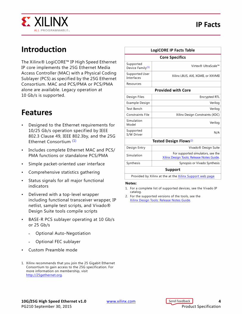
Introduction
The Xilinx® LogiCORE™ IP High Speed Ethernet IP core implements the 25G Ethernet Media Access Controller (MAC) with a Physical Coding Sublayer (PCS) as specified by the 25G Ethernet Consortium. MAC and PCS/PMA or PCS/PMA alone are available. Legacy operation at 10 Gb/s is supported.
Features
• Designed to the Ethernet requirements for 10/25 Gb/s operation specif ied by IEEE 802.3 Clause 49, IEEE 802.3by, and the 25G Ethernet Consortium (1)
• Includes complete Ethernet MAC and PCS/PMA functions or standalone PCS/PMA
• Simple packet-oriented user interface
• Comprehensive statistics gathering
• Status signals for all major functional indicators
• Delivered with a top-level wrapper including functional transceiver wrapper, IP netlist, sample test scripts, and Vivado® Design Suite tools compile scripts
• BASE-R PCS sublayer operating at 10 Gb/s or 25 Gb/s
° Optional Auto-Negotiation
° Optional FEC sublayer
• Custom Preamble mode
1. Xilinx recommends that you join the 25 Gigabit Ethernet Consortium to gain access to the 25G specif ication. For more information on membership, visit http://25gethernet.org.
IP Facts
LogiCORE IP Facts Table
Core Specifics
Supported Device Family(1) Virtex® UltraScale™
Supported User Interfaces Xilinx LBUS, AXI, XGMII, or XXVMII
Resources
Provided with Core
Design Files Encrypted RTL
Example Design Verilog
Test Bench Verilog
Constraints File Xilinx Design Constraints (XDC)
Simulation Model Verilog
Supported S/W Driver N/A
Tested Design Flows(2)
Design Entry Vivado® Design Suite
Simulation For supported simulators, see theXilinx Design Tools: Release Notes Guide.
Synthesis Synopsis or Vivado Synthesis
Support
Provided by Xilinx at the at the Xilinx Support web page
Notes: 1. For a complete list of supported devices, see the Vivado IP
catalog.2. For the supported versions of the tools, see the
Xilinx Design Tools: Release Notes Guide.
Send Feedback
10G/25G High Speed Ethernet v1.0 www.xilinx.com 5PG210 September 30, 2015
Chapter 1
OverviewThis document details the features of the 10G/25G Ethernet core as defined by the 25G Ethernet Consortium [Ref 1]. PCS functionality is defined by IEEE Standard 802.3, 2012, Section 4, Clause 49, Physical Coding Sublayer (PCS) for 64B/66B, type 10GBASE-R [Ref 2]. For 25G operation, clock frequencies are increased to provide a serial interface operating at 25.78125 Gb/s to leverage the latest high-speed serial transceivers. The low latency design is optimized for UltraScale™ architecture devices.
Feature Summary
25G Supported Features
• Complete Ethernet MAC and PCS functions
• Designed to Schedule 3 of the 25G Consortium
• Statistics and diagnostics
• 64-bit LBUS user interface at 390.625 MHz
• 66-bit SerDes interface using Xilinx GTY transceiver operating with Asynchronous Gearbox enabled
• Pause Processing including IEEE std. 802.3 Annex 31D (Priority based Flow Control)
• Low latency
• Custom preamble and adjustable Inter Frame Gap
• Configurable for operation at 10 Gb/s (Clause 49)
10G Supported Features
• Complete MAC and PCS functions
• IEEE 802.3 Clause 49
• Statistics and diagnostics
• 64-bit LBUS user interface at 156.25 MHz
• 66-bit SerDes interface
Send Feedback
10G/25G High Speed Ethernet v1.0 www.xilinx.com 6PG210 September 30, 2015
Chapter 1: Overview
• Custom preamble and adjustable Inter Frame Gap
Optional Features
• Clause 73 Auto-Negotiation
• Clause 72.6.10 Link Training
• Clause 74 FEC - shortened cyclic code (2112, 2080)
• PCS only version with XGMII/XXVMII interface (See the Port Descriptions – PCS Variant.)
• AXI-Stream interface (Available in future release)
• AXI4-Lite control and status interface
ApplicationsIEEE Std 802.3 enables several different Ethernet speeds for Local Area Network (LAN) applications, and 25 Gb/s is the latest addition to the standard. The capability to interconnect devices at 25 Gb/s Ethernet rates becomes especially relevant for next-generation data center networks where:
(i) To keep up with increasing CPU and storage bandwidth, rack or blade servers need to support aggregate throughputs faster than 10 Gb/s (single lane) or 20 Gb/s (dual lane) from their Network Interface Card (NIC) or LAN-on-Motherboard (LOM) networking ports;
(ii) Given the increased bandwidth to endpoints, uplinks from Top-of-Rack (TOR) or Blade switches need to transition from 40 Gb/s (four lanes) to 100 Gb/s (four lanes) while ideally maintaining the same per-lane breakout capability;
(iii) Due to the expected adoption of 100GBASE-CR4/KR4/SR4/LR4, SerDes and cabling technologies are already being developed and deployed to support 25 Gb/s per physical lane, twisted pair, or f iber.
Licensing and Ordering Information
License Checkers
If the IP requires a license key, the key must be verif ied. The Vivado® design tools have several license checkpoints for gating licensed IP through the flow. If the license check succeeds, the IP can continue generation. Otherwise, generation halts with error. License checkpoints are enforced by the following tools:
Send Feedback
10G/25G High Speed Ethernet v1.0 www.xilinx.com 7PG210 September 30, 2015
Chapter 1: Overview
• Vivado Synthesis
• Vivado Implementation
• write_bitstream (Tcl Console command)
IMPORTANT: IP license level is ignored at checkpoints. The test confirms a valid license exists. It does not check IP license level.
License Type
10G/25G Ethernet PCS/PMA (10G/25G BASE‐R)
This Xilinx LogiCORE™ IP module is provided at no additional cost with the Xilinx Vivado® Design Suite under the terms of the Xilinx End User License. Information about this and other Xilinx LogiCORE IP modules is available at the Xilinx Intellectual Property page. For information about pricing and availability of other Xilinx LogiCORE IP modules and tools, contact your local Xilinx sales representative.
For more information, visit the 10G/25G Ethernet product web page.
Standalone 10G/25G Ethernet MAC and PCS/PMA (10G/25G EMAC + 10G/25G BASE‐R/KR) 10G/25G BASE‐KR
This Xilinx LogiCORE IP module is provided under the terms of the Xilinx Core License Agreement. The module is shipped as part of the Vivado Design Suite. For full access to all core functionalities in simulation and in hardware, you must purchase one or more licenses for the core. Contact your local Xilinx sales representative for information about pricing and availability.
For more information, visit the 10G/25G Ethernet product web page.
Send Feedback
10G/25G High Speed Ethernet v1.0 www.xilinx.com 8PG210 September 30, 2015
Chapter 2
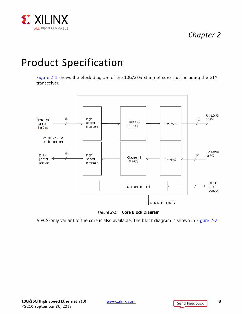
Product SpecificationFigure 2-1 shows the block diagram of the 10G/25G Ethernet core, not including the GTY transceiver.
A PCS-only variant of the core is also available. The block diagram is shown in Figure 2-2.
X-Ref Target - Figure 2-1
Figure 2‐1: Core Block Diagram
Send Feedback

10G/25G High Speed Ethernet v1.0 www.xilinx.com 9PG210 September 30, 2015
Chapter 2: Product Specification
StandardsThe 10G/25G Ethernet core is designed to the standard specif ied in the 25G and 50G Ethernet Consortium [Ref 1] and the IEEE Std 802.3 including IEEE 802.3by [Ref 2].
PerformanceThere is no information currently provided for this core.
Resource UtilizationTable 2-1 provides approximate resource counts for the various core options on Virtex® UltraScale™ devices.
X-Ref Target - Figure 2-2
Figure 2‐2: Block Diagram of PCS‐Only Core Variant
Send Feedback

10G/25G High Speed Ethernet v1.0 www.xilinx.com 10PG210 September 30, 2015
Chapter 2: Product Specification
Port DescriptionsThe following tables lists the ports for the 10G/25G Ethernet IP core with integrated MAC and PCS. These signals are found at the *wrapper.v hierarchy.
Transceiver Interface
Table 2-2 shows the transceiver I/O ports for the 10G/25G Ethernet IP core. Refer to Clocking in Chapter 3 for details regarding each clock domain.
Table 2‐1: Device Utilization – Virtex UltraScale FPGAs
LUT as Logic (k)
Register as Flip Flop (k)
Block RAM /MII width
LBUS/MII clk MHz AN, LT, FEC Gearbox
10.405 5.722 2 64 390.625 AN, LT,FEC IP
8.162 4.375 1 64 390.625 AN,LT IP
1.9 1.5 1 64 390.625 No GT
Table 2‐2: Transceiver I/O
Name Direction Description Clock Domain
ctl_gt_reset_all Input Active High asynchronous reset for the transceiver startup FSM. Note that this signal also initiates the reset sequence for the entire 10G/25G Ethernet IP core.
Asynch
refclk_n0 Input Differential reference clock input for the SerDes, negative phase.
Refer to Clocking.
refclk_p0 Input Differential reference clock input for the SerDes, positive phase.
Refer to Clocking.
rx_serdes_data_n0 Input Serial data from the line; negative phase of the differential signal
Refer to Clocking.
rx_serdes_data_p0 Input Serial data from the line; positive phase of the differential signal
Refer to Clocking.
tx_serdes_data_n0 Output Serial data to the line; negative phase of the differential signal.
Refer to Clocking.
tx_serdes_data_p0 Output Serial data to the line; positive phase of the differential signal.
Refer to Clocking.
tx_serdes_clkout Output When present, same as tx_clk_out. Refer to Clocking.
Send Feedback
10G/25G High Speed Ethernet v1.0 www.xilinx.com 11PG210 September 30, 2015
Chapter 2: Product Specification
LBUS Interface Ports
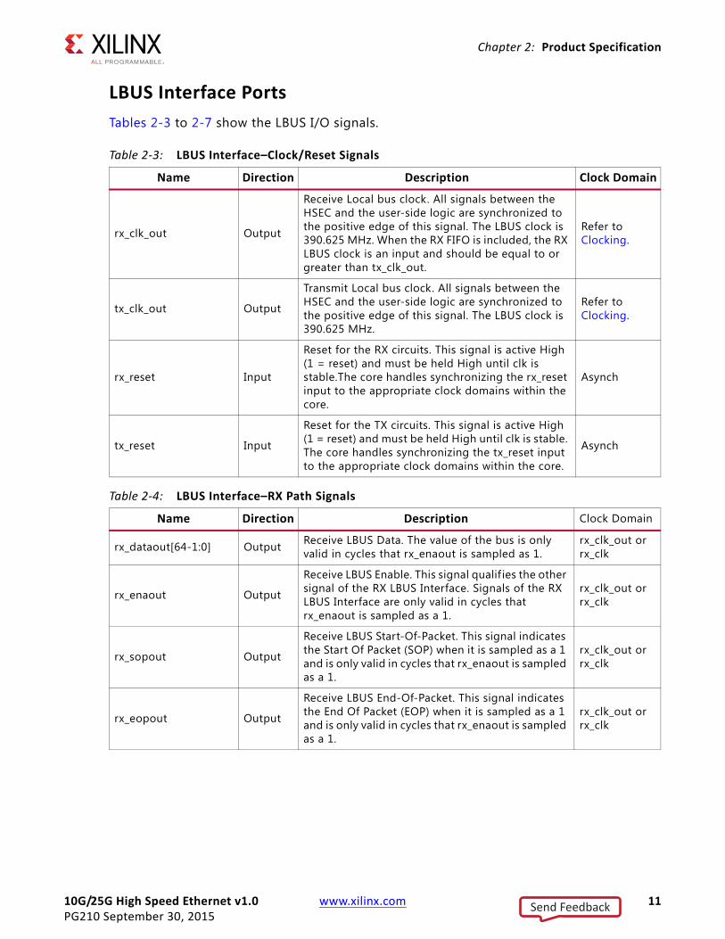
Tables 2-3 to 2-7 show the LBUS I/O signals.
Table 2‐3: LBUS Interface–Clock/Reset Signals
Name Direction Description Clock Domain
rx_clk_out Output
Receive Local bus clock. All signals between the HSEC and the user-side logic are synchronized to the positive edge of this signal. The LBUS clock is 390.625 MHz. When the RX FIFO is included, the RX LBUS clock is an input and should be equal to or greater than tx_clk_out.
Refer to Clocking.
tx_clk_out Output
Transmit Local bus clock. All signals between the HSEC and the user-side logic are synchronized to the positive edge of this signal. The LBUS clock is 390.625 MHz.
Refer to Clocking.
rx_reset Input
Reset for the RX circuits. This signal is active High (1 = reset) and must be held High until clk is stable.The core handles synchronizing the rx_reset input to the appropriate clock domains within the core.
Asynch
tx_reset Input
Reset for the TX circuits. This signal is active High (1 = reset) and must be held High until clk is stable. The core handles synchronizing the tx_reset input to the appropriate clock domains within the core.
Asynch
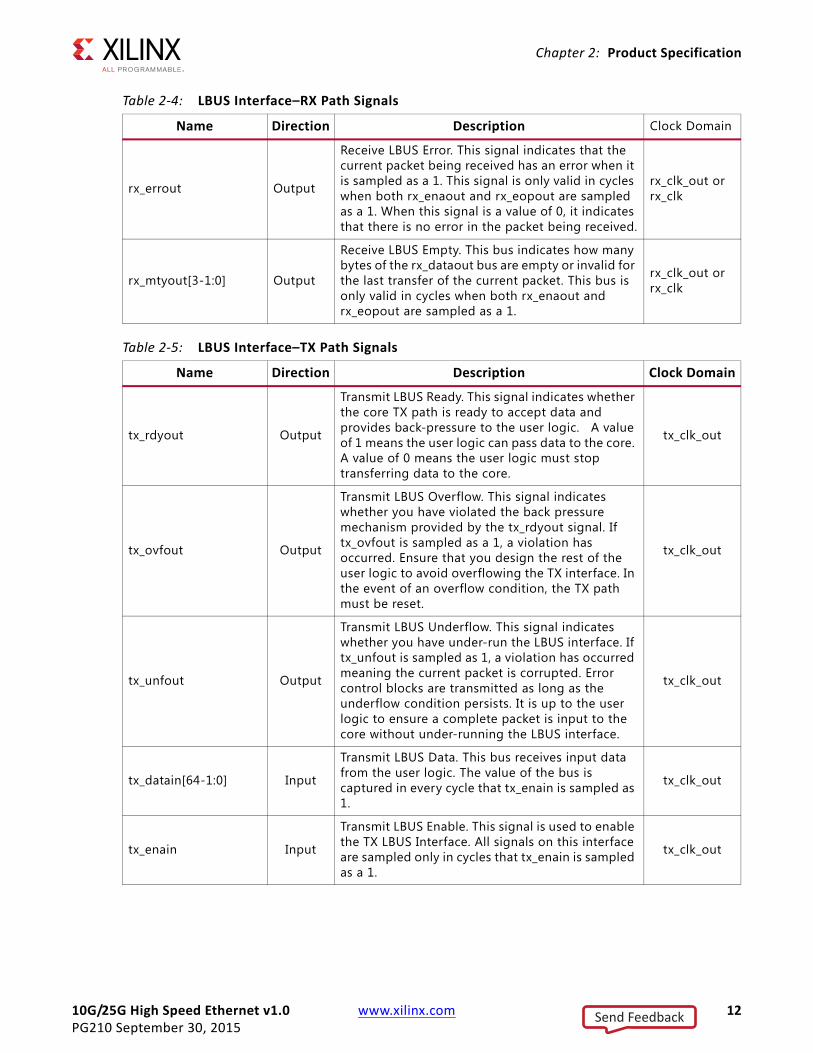
Table 2‐4: LBUS Interface–RX Path Signals
Name Direction Description Clock Domain
rx_dataout[64-1:0] Output Receive LBUS Data. The value of the bus is only valid in cycles that rx_enaout is sampled as 1.
rx_clk_out or rx_clk
rx_enaout Output
Receive LBUS Enable. This signal qualif ies the other signal of the RX LBUS Interface. Signals of the RX LBUS Interface are only valid in cycles that rx_enaout is sampled as a 1.
rx_clk_out or rx_clk
rx_sopout Output
Receive LBUS Start-Of-Packet. This signal indicates the Start Of Packet (SOP) when it is sampled as a 1 and is only valid in cycles that rx_enaout is sampled as a 1.
rx_clk_out or rx_clk
rx_eopout Output
Receive LBUS End-Of-Packet. This signal indicates the End Of Packet (EOP) when it is sampled as a 1 and is only valid in cycles that rx_enaout is sampled as a 1.
rx_clk_out or rx_clk
Send Feedback
10G/25G High Speed Ethernet v1.0 www.xilinx.com 12PG210 September 30, 2015
Chapter 2: Product Specification
rx_errout Output
Receive LBUS Error. This signal indicates that the current packet being received has an error when it is sampled as a 1. This signal is only valid in cycles when both rx_enaout and rx_eopout are sampled as a 1. When this signal is a value of 0, it indicates that there is no error in the packet being received.
rx_clk_out or rx_clk
rx_mtyout[3-1:0] Output
Receive LBUS Empty. This bus indicates how many bytes of the rx_dataout bus are empty or invalid for the last transfer of the current packet. This bus is only valid in cycles when both rx_enaout and rx_eopout are sampled as a 1.
rx_clk_out or rx_clk
Table 2‐5: LBUS Interface–TX Path Signals
Name Direction Description Clock Domain
tx_rdyout Output
Transmit LBUS Ready. This signal indicates whether the core TX path is ready to accept data and provides back-pressure to the user logic. A value of 1 means the user logic can pass data to the core. A value of 0 means the user logic must stop transferring data to the core.
tx_clk_out
tx_ovfout Output
Transmit LBUS Overflow. This signal indicates whether you have violated the back pressure mechanism provided by the tx_rdyout signal. If tx_ovfout is sampled as a 1, a violation has occurred. Ensure that you design the rest of the user logic to avoid overflowing the TX interface. In the event of an overflow condition, the TX path must be reset.
tx_clk_out
tx_unfout Output
Transmit LBUS Underflow. This signal indicates whether you have under-run the LBUS interface. If tx_unfout is sampled as 1, a violation has occurred meaning the current packet is corrupted. Error control blocks are transmitted as long as the underflow condition persists. It is up to the user logic to ensure a complete packet is input to the core without under-running the LBUS interface.
tx_clk_out
tx_datain[64-1:0] Input
Transmit LBUS Data. This bus receives input data from the user logic. The value of the bus is captured in every cycle that tx_enain is sampled as 1.
tx_clk_out
tx_enain Input
Transmit LBUS Enable. This signal is used to enable the TX LBUS Interface. All signals on this interface are sampled only in cycles that tx_enain is sampled as a 1.
tx_clk_out
Table 2‐4: LBUS Interface–RX Path Signals
Name Direction Description Clock Domain
Send Feedback
10G/25G High Speed Ethernet v1.0 www.xilinx.com 13PG210 September 30, 2015
Chapter 2: Product Specification
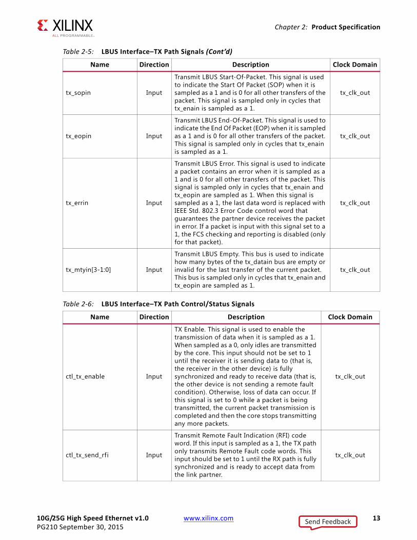
tx_sopin Input
Transmit LBUS Start-Of-Packet. This signal is used to indicate the Start Of Packet (SOP) when it is sampled as a 1 and is 0 for all other transfers of the packet. This signal is sampled only in cycles that tx_enain is sampled as a 1.
tx_clk_out
tx_eopin Input
Transmit LBUS End-Of-Packet. This signal is used to indicate the End Of Packet (EOP) when it is sampled as a 1 and is 0 for all other transfers of the packet. This signal is sampled only in cycles that tx_enain is sampled as a 1.
tx_clk_out
tx_errin Input
Transmit LBUS Error. This signal is used to indicate a packet contains an error when it is sampled as a 1 and is 0 for all other transfers of the packet. This signal is sampled only in cycles that tx_enain and tx_eopin are sampled as 1. When this signal is sampled as a 1, the last data word is replaced with IEEE Std. 802.3 Error Code control word that guarantees the partner device receives the packet in error. If a packet is input with this signal set to a 1, the FCS checking and reporting is disabled (only for that packet).
tx_clk_out
tx_mtyin[3-1:0] Input
Transmit LBUS Empty. This bus is used to indicate how many bytes of the tx_datain bus are empty or invalid for the last transfer of the current packet. This bus is sampled only in cycles that tx_enain and tx_eopin are sampled as 1.
tx_clk_out
Table 2‐6: LBUS Interface–TX Path Control/Status Signals
Name Direction Description Clock Domain
ctl_tx_enable Input
TX Enable. This signal is used to enable the transmission of data when it is sampled as a 1. When sampled as a 0, only idles are transmitted by the core. This input should not be set to 1 until the receiver it is sending data to (that is, the receiver in the other device) is fully synchronized and ready to receive data (that is, the other device is not sending a remote fault condition). Otherwise, loss of data can occur. If this signal is set to 0 while a packet is being transmitted, the current packet transmission is completed and then the core stops transmitting any more packets.
tx_clk_out
ctl_tx_send_rfi Input
Transmit Remote Fault Indication (RFI) code word. If this input is sampled as a 1, the TX path only transmits Remote Fault code words. This input should be set to 1 until the RX path is fully synchronized and is ready to accept data from the link partner.
tx_clk_out
Table 2‐5: LBUS Interface–TX Path Signals (Cont’d)
Name Direction Description Clock Domain
Send Feedback
10G/25G High Speed Ethernet v1.0 www.xilinx.com 14PG210 September 30, 2015
Chapter 2: Product Specification
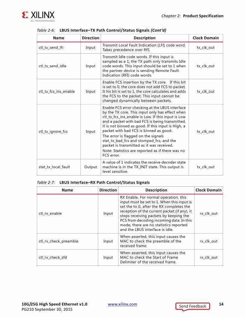
ctl_tx_send_lf i Input Transmit Local Fault Indication (LFI) code word. Takes precedence over RFI. tx_clk_out
ctl_tx_send_idle Input
Transmit Idle code words. If this input is sampled as a 1, the TX path only transmits Idle code words. This input should be set to 1 when the partner device is sending Remote Fault Indication (RFI) code words.
tx_clk_out
ctl_tx_fcs_ins_enable Input
Enable FCS insertion by the TX core. If this bit is set to 0, the core does not add FCS to packet. It his bit is set to 1, the core calculates and adds the FCS to the packet. This input cannot be changed dynamically between packets.
tx_clk_out
ctl_tx_ignore_fcs Input
Enable FCS error checking at the LBUS interface by the TX core. This input only has effect when ctl_tx_fcs_ins_enable is Low. If this input is Low and a packet with bad FCS is being transmitted, it is not binned as good. If this input is High, a packet with bad FCS is binned as good.The error is flagged on the signals stat_tx_bad_fcs and stomped_fcs, and the packet is transmitted as it was received.Note: Statistics are reported as if there was no FCS error.
tx_clk_out
stat_tx_local_fault OutputA value of 1 indicates the receive decoder state machine is in the TX_INIT state. This output is level sensitive.
tx_clk_out
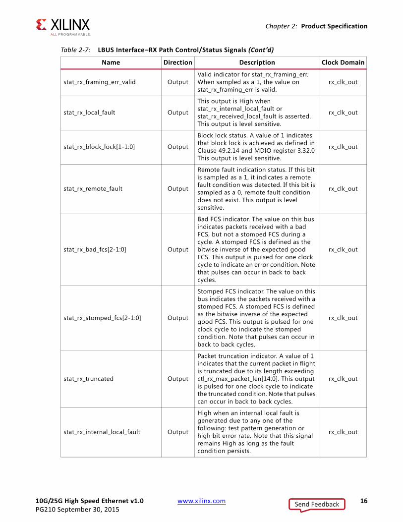
Table 2‐7: LBUS Interface–RX Path Control/Status Signals
Name Direction Description Clock Domain
ctl_rx_enable Input
RX Enable. For normal operation, this input must be set to 1. When this input is set the to 0, after the RX completes the reception of the current packet (if any), it stops receiving packets by keeping the PCS from decoding incoming data. In this mode, there are no statistics reported and the LBUS interface is idle.
rx_clk_out
ctl_rx_check_preamble InputWhen asserted, this input causes the MAC to check the preamble of the received frame.
rx_clk_out
ctl_rx_check_sfd InputWhen asserted, this input causes the MAC to check the Start of Frame Delimiter of the received frame.
rx_clk_out
Table 2‐6: LBUS Interface–TX Path Control/Status Signals (Cont’d)
Name Direction Description Clock Domain
Send Feedback
10G/25G High Speed Ethernet v1.0 www.xilinx.com 15PG210 September 30, 2015
Chapter 2: Product Specification
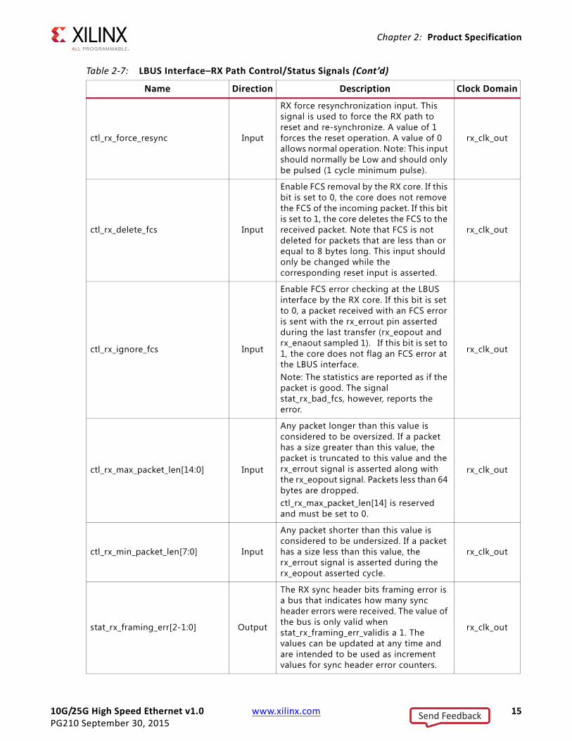
ctl_rx_force_resync Input
RX force resynchronization input. This signal is used to force the RX path to reset and re-synchronize. A value of 1 forces the reset operation. A value of 0 allows normal operation. Note: This input should normally be Low and should only be pulsed (1 cycle minimum pulse).
rx_clk_out
ctl_rx_delete_fcs Input
Enable FCS removal by the RX core. If this bit is set to 0, the core does not remove the FCS of the incoming packet. If this bit is set to 1, the core deletes the FCS to the received packet. Note that FCS is not deleted for packets that are less than or equal to 8 bytes long. This input should only be changed while the corresponding reset input is asserted.
rx_clk_out
ctl_rx_ignore_fcs Input
Enable FCS error checking at the LBUS interface by the RX core. If this bit is set to 0, a packet received with an FCS error is sent with the rx_errout pin asserted during the last transfer (rx_eopout and rx_enaout sampled 1). If this bit is set to 1, the core does not flag an FCS error at the LBUS interface.Note: The statistics are reported as if the packet is good. The signal stat_rx_bad_fcs, however, reports the error.
rx_clk_out
ctl_rx_max_packet_len[14:0] Input
Any packet longer than this value is considered to be oversized. If a packet has a size greater than this value, the packet is truncated to this value and the rx_errout signal is asserted along with the rx_eopout signal. Packets less than 64 bytes are dropped.ctl_rx_max_packet_len[14] is reserved and must be set to 0.
rx_clk_out
ctl_rx_min_packet_len[7:0] Input
Any packet shorter than this value is considered to be undersized. If a packet has a size less than this value, the rx_errout signal is asserted during the rx_eopout asserted cycle.
rx_clk_out
stat_rx_framing_err[2-1:0] Output
The RX sync header bits framing error is a bus that indicates how many sync header errors were received. The value of the bus is only valid when stat_rx_framing_err_validis a 1. The values can be updated at any time and are intended to be used as increment values for sync header error counters.
rx_clk_out
Table 2‐7: LBUS Interface–RX Path Control/Status Signals (Cont’d)
Name Direction Description Clock Domain
Send Feedback
10G/25G High Speed Ethernet v1.0 www.xilinx.com 16PG210 September 30, 2015
Chapter 2: Product Specification
stat_rx_framing_err_valid OutputValid indicator for stat_rx_framing_err. When sampled as a 1, the value on stat_rx_framing_err is valid.
rx_clk_out
stat_rx_local_fault Output
This output is High when stat_rx_internal_local_fault or stat_rx_received_local_fault is asserted. This output is level sensitive.
rx_clk_out
stat_rx_block_lock[1-1:0] Output
Block lock status. A value of 1 indicates that block lock is achieved as defined in Clause 49.2.14 and MDIO register 3.32.0 This output is level sensitive.
rx_clk_out
stat_rx_remote_fault Output
Remote fault indication status. If this bit is sampled as a 1, it indicates a remote fault condition was detected. If this bit is sampled as a 0, remote fault condition does not exist. This output is level sensitive.
rx_clk_out
stat_rx_bad_fcs[2-1:0] Output
Bad FCS indicator. The value on this bus indicates packets received with a bad FCS, but not a stomped FCS during a cycle. A stomped FCS is defined as the bitwise inverse of the expected good FCS. This output is pulsed for one clock cycle to indicate an error condition. Note that pulses can occur in back to back cycles.
rx_clk_out
stat_rx_stomped_fcs[2-1:0] Output
Stomped FCS indicator. The value on this bus indicates the packets received with a stomped FCS. A stomped FCS is defined as the bitwise inverse of the expected good FCS. This output is pulsed for one clock cycle to indicate the stomped condition. Note that pulses can occur in back to back cycles.
rx_clk_out
stat_rx_truncated Output
Packet truncation indicator. A value of 1 indicates that the current packet in flight is truncated due to its length exceeding ctl_rx_max_packet_len[14:0]. This output is pulsed for one clock cycle to indicate the truncated condition. Note that pulses can occur in back to back cycles.
rx_clk_out
stat_rx_internal_local_fault Output
High when an internal local fault is generated due to any one of the following: test pattern generation or high bit error rate. Note that this signal remains High as long as the fault condition persists.
rx_clk_out
Table 2‐7: LBUS Interface–RX Path Control/Status Signals (Cont’d)
Name Direction Description Clock Domain
Send Feedback
10G/25G High Speed Ethernet v1.0 www.xilinx.com 17PG210 September 30, 2015
Chapter 2: Product Specification
Miscellaneous Status/Control Signals
Table 2-8 shows the miscellaneous status and control I/O signals.
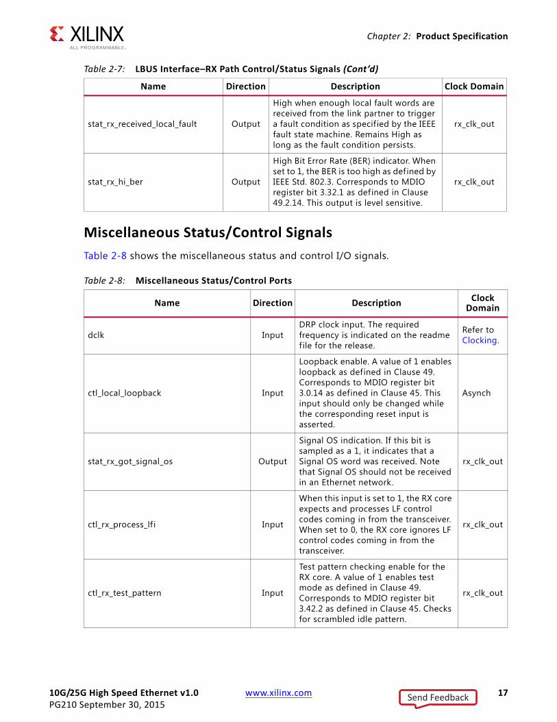
stat_rx_received_local_fault Output
High when enough local fault words are received from the link partner to trigger a fault condition as specif ied by the IEEE fault state machine. Remains High as long as the fault condition persists.
rx_clk_out
stat_rx_hi_ber Output
High Bit Error Rate (BER) indicator. When set to 1, the BER is too high as defined by IEEE Std. 802.3. Corresponds to MDIO register bit 3.32.1 as defined in Clause 49.2.14. This output is level sensitive.
rx_clk_out
Table 2‐8: Miscellaneous Status/Control Ports
Name Direction Description Clock Domain
dclk InputDRP clock input. The required frequency is indicated on the readme file for the release.
Refer to Clocking.
ctl_local_loopback Input
Loopback enable. A value of 1 enables loopback as defined in Clause 49. Corresponds to MDIO register bit 3.0.14 as defined in Clause 45. This input should only be changed while the corresponding reset input is asserted.
Asynch
stat_rx_got_signal_os Output
Signal OS indication. If this bit is sampled as a 1, it indicates that a Signal OS word was received. Note that Signal OS should not be received in an Ethernet network.
rx_clk_out
ctl_rx_process_lf i Input
When this input is set to 1, the RX core expects and processes LF control codes coming in from the transceiver. When set to 0, the RX core ignores LF control codes coming in from the transceiver.
rx_clk_out
ctl_rx_test_pattern Input
Test pattern checking enable for the RX core. A value of 1 enables test mode as defined in Clause 49. Corresponds to MDIO register bit 3.42.2 as defined in Clause 45. Checks for scrambled idle pattern.
rx_clk_out
Table 2‐7: LBUS Interface–RX Path Control/Status Signals (Cont’d)
Name Direction Description Clock Domain
Send Feedback
10G/25G High Speed Ethernet v1.0 www.xilinx.com 18PG210 September 30, 2015
Chapter 2: Product Specification
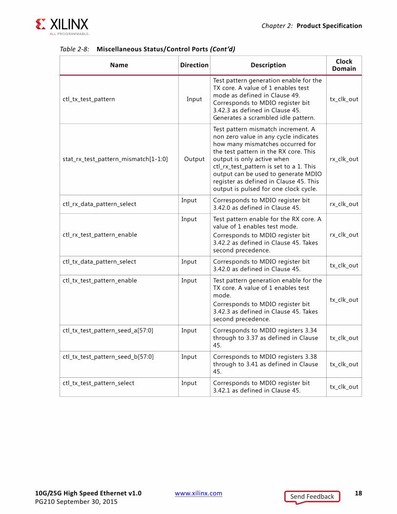
ctl_tx_test_pattern Input
Test pattern generation enable for the TX core. A value of 1 enables test mode as defined in Clause 49. Corresponds to MDIO register bit 3.42.3 as defined in Clause 45. Generates a scrambled idle pattern.
tx_clk_out
stat_rx_test_pattern_mismatch[1-1:0] Output
Test pattern mismatch increment. A non zero value in any cycle indicates how many mismatches occurred for the test pattern in the RX core. This output is only active when ctl_rx_test_pattern is set to a 1. This output can be used to generate MDIO register as defined in Clause 45. This output is pulsed for one clock cycle.
rx_clk_out
ctl_rx_data_pattern_select Input Corresponds to MDIO register bit 3.42.0 as defined in Clause 45. rx_clk_out
ctl_rx_test_pattern_enable
Input Test pattern enable for the RX core. A value of 1 enables test mode.Corresponds to MDIO register bit 3.42.2 as defined in Clause 45. Takes second precedence.
rx_clk_out
ctl_tx_data_pattern_select Input Corresponds to MDIO register bit 3.42.0 as defined in Clause 45. tx_clk_out
ctl_tx_test_pattern_enable Input Test pattern generation enable for the TX core. A value of 1 enables test mode.Corresponds to MDIO register bit 3.42.3 as defined in Clause 45. Takes second precedence.
tx_clk_out
ctl_tx_test_pattern_seed_a[57:0] Input Corresponds to MDIO registers 3.34 through to 3.37 as defined in Clause 45.
tx_clk_out
ctl_tx_test_pattern_seed_b[57:0] Input Corresponds to MDIO registers 3.38 through to 3.41 as defined in Clause 45.
tx_clk_out
ctl_tx_test_pattern_select Input Corresponds to MDIO register bit 3.42.1 as defined in Clause 45. tx_clk_out
Table 2‐8: Miscellaneous Status/Control Ports (Cont’d)
Name Direction Description Clock Domain
Send Feedback

10G/25G High Speed Ethernet v1.0 www.xilinx.com 19PG210 September 30, 2015
Chapter 2: Product Specification
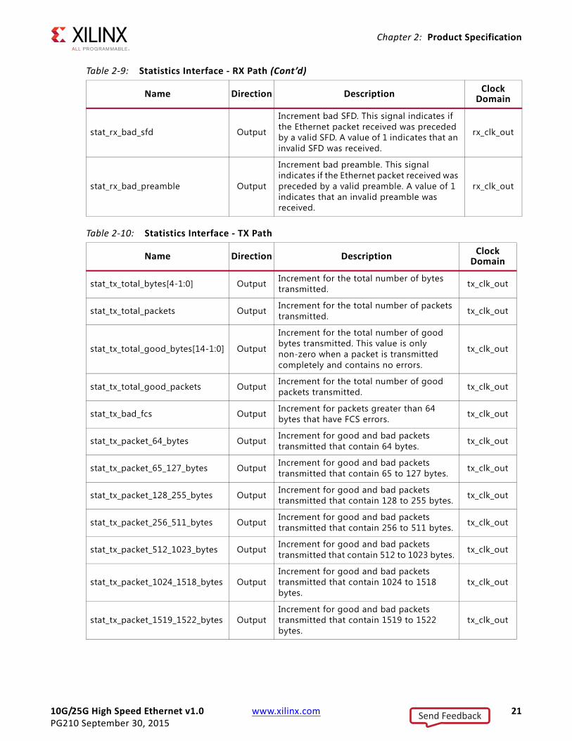
Statistics Interface Ports
Tables 2-9 to 2-10 show the Statistics interface I/O ports.
Table 2‐9: Statistics Interface ‐ RX Path
Name Direction DescriptionClock
Domain
stat_rx_total_bytes[4-1:0] Output Increment for the total number of bytes received. rx_clk_out
stat_rx_total_packets[2-1:0] Output Increment for the total number of packets received. rx_clk_out
stat_rx_total_good_bytes[14-1:0] Output
Increment for the total number of good bytes received. This value is only non-zero when a packet is received completely and contains no errors.
rx_clk_out
stat_rx_total_good_packets Output
Increment for the total number of good packets received. This value is only non-zero when a packet is received completely and contains no errors.
rx_clk_out
stat_rx_packet_bad_fcs OutputIncrement for packets between 64 and ctl_rx_max_packet_len bytes that have FCS errors.
rx_clk_out
stat_rx_packet_64_bytes Output Increment for good and bad packets received that contain 64 bytes. rx_clk_out
stat_rx_packet_65_127_bytes Output Increment for good and bad packets received that contain 65 to 127 bytes. rx_clk_out
stat_rx_packet_128_255_bytes Output Increment for good and bad packets received that contain 128 to 255 bytes. rx_clk_out
stat_rx_packet_256_511_bytes Output Increment for good and bad packets received that contain 256 to 511 bytes. rx_clk_out
stat_rx_packet_512_1023_bytes Output Increment for good and bad packets received that contain 512 to 1023 bytes. rx_clk_out
stat_rx_packet_1024_1518_bytes Output Increment for good and bad packets received that contain 1024 to 1518 bytes. rx_clk_out
stat_rx_packet_1519_1522_bytes Output Increment for good and bad packets received that contain 1519 to 1522 bytes. rx_clk_out
stat_rx_packet_1523_1548_bytes Output Increment for good and bad packets received that contain 1523 to 1548 bytes. rx_clk_out
stat_rx_packet_1549_2047_bytes Output Increment for good and bad packets received that contain 1549 to 2047 bytes. rx_clk_out
stat_rx_packet_2048_4095_bytes Output Increment for good and bad packets received that contain 2048 to 4095 bytes. rx_clk_out
stat_rx_packet_4096_8191_bytes Output Increment for good and bad packets received that contain 4096 to 8191 bytes. rx_clk_out
Send Feedback
10G/25G High Speed Ethernet v1.0 www.xilinx.com 20PG210 September 30, 2015
Chapter 2: Product Specification
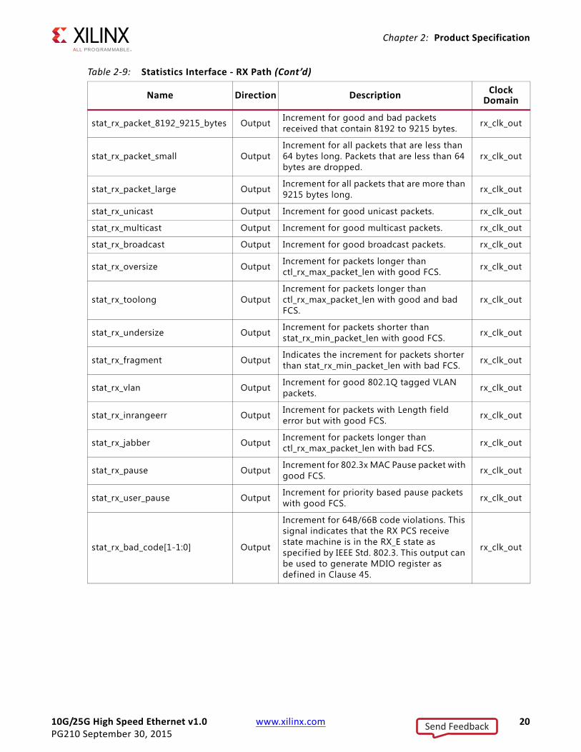
stat_rx_packet_8192_9215_bytes Output Increment for good and bad packets received that contain 8192 to 9215 bytes. rx_clk_out
stat_rx_packet_small OutputIncrement for all packets that are less than 64 bytes long. Packets that are less than 64 bytes are dropped.
rx_clk_out
stat_rx_packet_large Output Increment for all packets that are more than 9215 bytes long. rx_clk_out
stat_rx_unicast Output Increment for good unicast packets. rx_clk_out
stat_rx_multicast Output Increment for good multicast packets. rx_clk_out
stat_rx_broadcast Output Increment for good broadcast packets. rx_clk_out
stat_rx_oversize Output Increment for packets longer than ctl_rx_max_packet_len with good FCS. rx_clk_out
stat_rx_toolong OutputIncrement for packets longer than ctl_rx_max_packet_len with good and bad FCS.
rx_clk_out
stat_rx_undersize Output Increment for packets shorter than stat_rx_min_packet_len with good FCS. rx_clk_out
stat_rx_fragment Output Indicates the increment for packets shorter than stat_rx_min_packet_len with bad FCS. rx_clk_out
stat_rx_vlan Output Increment for good 802.1Q tagged VLAN packets. rx_clk_out
stat_rx_inrangeerr Output Increment for packets with Length field error but with good FCS. rx_clk_out
stat_rx_jabber Output Increment for packets longer than ctl_rx_max_packet_len with bad FCS. rx_clk_out
stat_rx_pause Output Increment for 802.3x MAC Pause packet with good FCS. rx_clk_out
stat_rx_user_pause Output Increment for priority based pause packets with good FCS. rx_clk_out
stat_rx_bad_code[1-1:0] Output
Increment for 64B/66B code violations. This signal indicates that the RX PCS receive state machine is in the RX_E state as specif ied by IEEE Std. 802.3. This output can be used to generate MDIO register as defined in Clause 45.
rx_clk_out
Table 2‐9: Statistics Interface ‐ RX Path (Cont’d)
Name Direction Description Clock Domain
Send Feedback
10G/25G High Speed Ethernet v1.0 www.xilinx.com 21PG210 September 30, 2015
Chapter 2: Product Specification
stat_rx_bad_sfd Output
Increment bad SFD. This signal indicates if the Ethernet packet received was preceded by a valid SFD. A value of 1 indicates that an invalid SFD was received.
rx_clk_out
stat_rx_bad_preamble Output
Increment bad preamble. This signal indicates if the Ethernet packet received was preceded by a valid preamble. A value of 1 indicates that an invalid preamble was received.
rx_clk_out
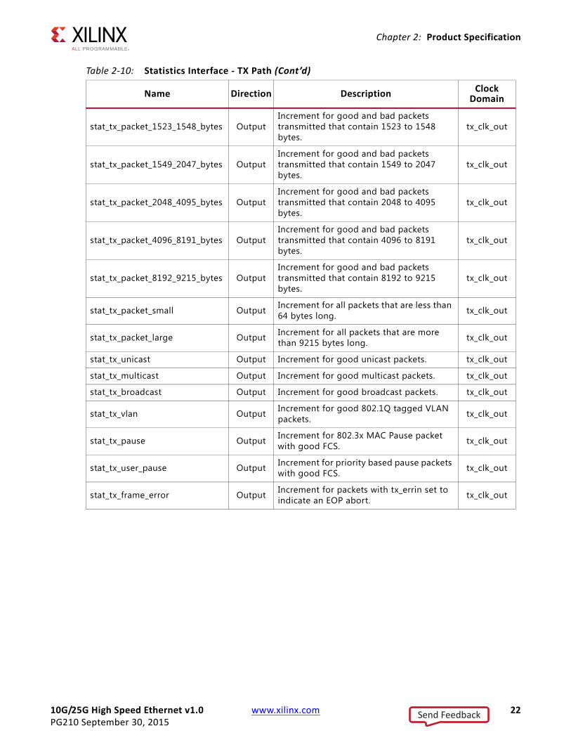
Table 2‐10: Statistics Interface ‐ TX Path
Name Direction DescriptionClock
Domain
stat_tx_total_bytes[4-1:0] Output Increment for the total number of bytes transmitted. tx_clk_out
stat_tx_total_packets Output Increment for the total number of packets transmitted. tx_clk_out
stat_tx_total_good_bytes[14-1:0] Output
Increment for the total number of good bytes transmitted. This value is only non-zero when a packet is transmitted completely and contains no errors.
tx_clk_out
stat_tx_total_good_packets Output Increment for the total number of good packets transmitted. tx_clk_out
stat_tx_bad_fcs Output Increment for packets greater than 64 bytes that have FCS errors. tx_clk_out
stat_tx_packet_64_bytes Output Increment for good and bad packets transmitted that contain 64 bytes. tx_clk_out
stat_tx_packet_65_127_bytes Output Increment for good and bad packets transmitted that contain 65 to 127 bytes. tx_clk_out
stat_tx_packet_128_255_bytes Output Increment for good and bad packets transmitted that contain 128 to 255 bytes. tx_clk_out
stat_tx_packet_256_511_bytes Output Increment for good and bad packets transmitted that contain 256 to 511 bytes. tx_clk_out
stat_tx_packet_512_1023_bytes Output Increment for good and bad packets transmitted that contain 512 to 1023 bytes. tx_clk_out
stat_tx_packet_1024_1518_bytes OutputIncrement for good and bad packets transmitted that contain 1024 to 1518 bytes.
tx_clk_out
stat_tx_packet_1519_1522_bytes OutputIncrement for good and bad packets transmitted that contain 1519 to 1522 bytes.
tx_clk_out
Table 2‐9: Statistics Interface ‐ RX Path (Cont’d)
Name Direction Description Clock Domain
Send Feedback
10G/25G High Speed Ethernet v1.0 www.xilinx.com 22PG210 September 30, 2015
Chapter 2: Product Specification
stat_tx_packet_1523_1548_bytes OutputIncrement for good and bad packets transmitted that contain 1523 to 1548 bytes.
tx_clk_out
stat_tx_packet_1549_2047_bytes OutputIncrement for good and bad packets transmitted that contain 1549 to 2047 bytes.
tx_clk_out
stat_tx_packet_2048_4095_bytes OutputIncrement for good and bad packets transmitted that contain 2048 to 4095 bytes.
tx_clk_out
stat_tx_packet_4096_8191_bytes OutputIncrement for good and bad packets transmitted that contain 4096 to 8191 bytes.
tx_clk_out
stat_tx_packet_8192_9215_bytes OutputIncrement for good and bad packets transmitted that contain 8192 to 9215 bytes.
tx_clk_out
stat_tx_packet_small Output Increment for all packets that are less than 64 bytes long. tx_clk_out
stat_tx_packet_large Output Increment for all packets that are more than 9215 bytes long. tx_clk_out
stat_tx_unicast Output Increment for good unicast packets. tx_clk_out
stat_tx_multicast Output Increment for good multicast packets. tx_clk_out
stat_tx_broadcast Output Increment for good broadcast packets. tx_clk_out
stat_tx_vlan Output Increment for good 802.1Q tagged VLAN packets. tx_clk_out
stat_tx_pause Output Increment for 802.3x MAC Pause packet with good FCS. tx_clk_out
stat_tx_user_pause Output Increment for priority based pause packets with good FCS. tx_clk_out
stat_tx_frame_error Output Increment for packets with tx_errin set to indicate an EOP abort. tx_clk_out
Table 2‐10: Statistics Interface ‐ TX Path (Cont’d)
Name Direction Description Clock Domain
Send Feedback

10G/25G High Speed Ethernet v1.0 www.xilinx.com 23PG210 September 30, 2015
Chapter 2: Product Specification
Pause Interface
Tables 2-11 to 2-13 show the Pause interface I/O ports.
Table 2‐11: Pause Interface–Control Ports
Name Direction DescriptionClock
Domain
ctl_rx_pause_enable[9-1:0] Input
RX pause enable signal. This input is used to enable the processing of the pause quanta for the corresponding priority. Note that this signal only affects the RX user interface, not the pause processing logic.
rx_clk_out
ctl_tx_pause_enable[9-1:0] Input
TX pause enable signal. This input is used to enable the processing of the pause quanta for the corresponding priority. This signal gates transmission of pause packets.
tx_clk_out
Table 2‐12: Pause Interface–RX Path
Name Direction Description Clock Domain
ctl_rx_enable_gcp Input A value of 1 enables global control packet processing. rx_clk_out
ctl_rx_check_mcast_gcp Input A value of 1 enables global control multicast destination address processing. rx_clk_out
ctl_rx_check_ucast_gcp Input A value of 1 enables global control unicast destination address processing. rx_clk_out
ctl_rx_pause_da_ucast[47:0] Input Unicast destination address for pause processing. rx_clk_out
ctl_rx_check_sa_gcp Input A value of 1 enables global control source address processing. rx_clk_out
ctl_rx_pause_sa[47:0] Input Source address for pause processing. rx_clk_out
ctl_rx_check_etype_gcp Input A value of 1 enables global control ethertype processing. rx_clk_out
ctl_rx_check_opcode_gcp Input A value of 1 enables global control opcode processing. rx_clk_out
ctl_rx_opcode_min_gcp[15:0] Input Minimum global control opcode value. rx_clk_out
ctl_rx_opcode_max_gcp[15:0] Input Maximum global control opcode value. rx_clk_out
ctl_rx_etype_gcp[15:0] Input Ethertype f ield for global control processing. rx_clk_out
ctl_rx_enable_pcp Input A value of 1 enables priority control packet processing. rx_clk_out
ctl_rx_check_mcast_pcp Input A value of 1 enables priority control multicast destination address processing. rx_clk_out
ctl_rx_check_ucast_pcp Input A value of 1 enables priority control unicast destination address processing. rx_clk_out
Send Feedback

10G/25G High Speed Ethernet v1.0 www.xilinx.com 24PG210 September 30, 2015
Chapter 2: Product Specification
ctl_rx_pause_da_mcast[47:0] Input Multicast destination address for pause processing. rx_clk_out
ctl_rx_check_sa_pcp Input A value of 1 enables priority control source address processing. rx_clk_out
ctl_rx_check_etype_pcp Input A value of 1 enables priority control ethertype processing. rx_clk_out
ctl_rx_etype_pcp[15:0] Input Ethertype f ield for priority control processing. rx_clk_out
ctl_rx_check_opcode_pcp Input A value of 1 enables priority control opcode processing. rx_clk_out
ctl_rx_opcode_min_pcp[15:0] Input Minimum priority control opcode value. rx_clk_out
ctl_rx_opcode_max_pcp[15:0] Input Maximum priority control opcode value. rx_clk_out
ctl_rx_enable_gpp Input A value of 1 enables global pause packet processing. rx_clk_out
ctl_rx_check_mcast_gpp Input A value of 1 enables global pause multicast destination address processing. rx_clk_out
ctl_rx_check_ucast_gpp Input A value of 1 enables global pause unicast destination address processing. rx_clk_out
ctl_rx_check_sa_gpp Input A value of 1 enables global pause source address processing. rx_clk_out
ctl_rx_check_etype_gpp Input A value of 1 enables global pause ethertype processing. rx_clk_out
ctl_rx_etype_gpp[15:0] Input Ethertype f ield for global pause processing. rx_clk_out
ctl_rx_check_opcode_gpp Input A value of 1 enables global pause opcode processing. rx_clk_out
ctl_rx_opcode_gpp[15:0] Input Global pause opcode value. rx_clk_out
ctl_rx_enable_ppp Input A value of 1 enables priority pause packet processing. rx_clk_out
ctl_rx_check_mcast_ppp Input A value of 1 enables priority pause multicast destination address processing. rx_clk_out
ctl_rx_check_ucast_ppp Input A value of 1 enables priority pause unicast destination address processing. rx_clk_out
ctl_rx_check_sa_ppp Input A value of 1 enables priority pause source address processing. rx_clk_out
ctl_rx_check_etype_ppp Input A value of 1 enables priority pause ethertype processing. rx_clk_out
ctl_rx_etype_ppp[15:0] Input Ethertype f ield for priority pause processing. rx_clk_out
ctl_rx_check_opcode_ppp Input A value of 1 enables priority pause opcode processing. rx_clk_out
Table 2‐12: Pause Interface–RX Path (Cont’d)
Name Direction Description Clock Domain
Send Feedback
10G/25G High Speed Ethernet v1.0 www.xilinx.com 25PG210 September 30, 2015
Chapter 2: Product Specification
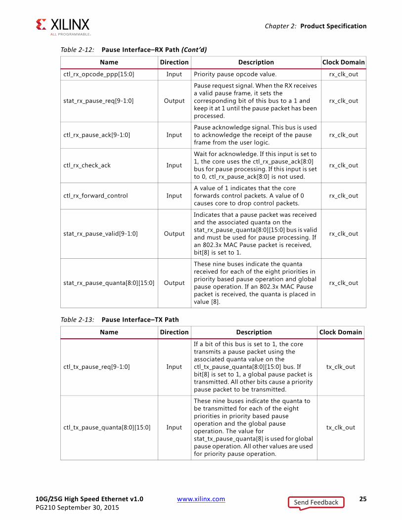
ctl_rx_opcode_ppp[15:0] Input Priority pause opcode value. rx_clk_out
stat_rx_pause_req[9-1:0] Output
Pause request signal. When the RX receives a valid pause frame, it sets the corresponding bit of this bus to a 1 and keep it at 1 until the pause packet has been processed.
rx_clk_out
ctl_rx_pause_ack[9-1:0] InputPause acknowledge signal. This bus is used to acknowledge the receipt of the pause frame from the user logic.
rx_clk_out
ctl_rx_check_ack Input
Wait for acknowledge. If this input is set to 1, the core uses the ctl_rx_pause_ack[8:0] bus for pause processing. If this input is set to 0, ctl_rx_pause_ack[8:0] is not used.
rx_clk_out
ctl_rx_forward_control InputA value of 1 indicates that the core forwards control packets. A value of 0 causes core to drop control packets.
rx_clk_out
stat_rx_pause_valid[9-1:0] Output
Indicates that a pause packet was received and the associated quanta on the stat_rx_pause_quanta[8:0][15:0] bus is valid and must be used for pause processing. If an 802.3x MAC Pause packet is received, bit[8] is set to 1.
rx_clk_out
stat_rx_pause_quanta[8:0][15:0] Output
These nine buses indicate the quanta received for each of the eight priorities in priority based pause operation and global pause operation. If an 802.3x MAC Pause packet is received, the quanta is placed in value [8].
rx_clk_out
Table 2‐13: Pause Interface–TX Path
Name Direction Description Clock Domain
ctl_tx_pause_req[9-1:0] Input
If a bit of this bus is set to 1, the core transmits a pause packet using the associated quanta value on the ctl_tx_pause_quanta[8:0][15:0] bus. If bit[8] is set to 1, a global pause packet is transmitted. All other bits cause a priority pause packet to be transmitted.
tx_clk_out
ctl_tx_pause_quanta[8:0][15:0] Input
These nine buses indicate the quanta to be transmitted for each of the eight priorities in priority based pause operation and the global pause operation. The value for stat_tx_pause_quanta[8] is used for global pause operation. All other values are used for priority pause operation.
tx_clk_out
Table 2‐12: Pause Interface–RX Path (Cont’d)
Name Direction Description Clock Domain
Send Feedback
10G/25G High Speed Ethernet v1.0 www.xilinx.com 26PG210 September 30, 2015
Chapter 2: Product Specification
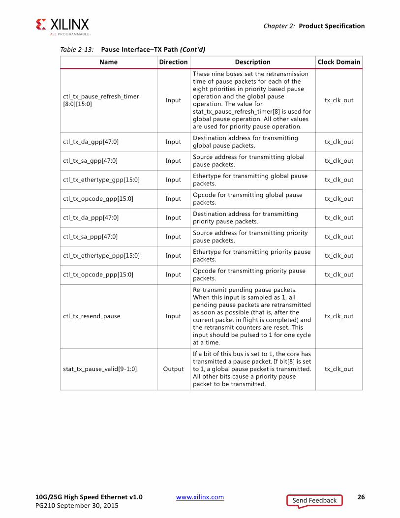
ctl_tx_pause_refresh_timer[8:0][15:0] Input
These nine buses set the retransmission time of pause packets for each of the eight priorities in priority based pause operation and the global pause operation. The value for stat_tx_pause_refresh_timer[8] is used for global pause operation. All other values are used for priority pause operation.
tx_clk_out
ctl_tx_da_gpp[47:0] Input Destination address for transmitting global pause packets. tx_clk_out
ctl_tx_sa_gpp[47:0] Input Source address for transmitting global pause packets. tx_clk_out
ctl_tx_ethertype_gpp[15:0] Input Ethertype for transmitting global pause packets. tx_clk_out
ctl_tx_opcode_gpp[15:0] Input Opcode for transmitting global pause packets. tx_clk_out
ctl_tx_da_ppp[47:0] Input Destination address for transmitting priority pause packets. tx_clk_out
ctl_tx_sa_ppp[47:0] Input Source address for transmitting priority pause packets. tx_clk_out
ctl_tx_ethertype_ppp[15:0] Input Ethertype for transmitting priority pause packets. tx_clk_out
ctl_tx_opcode_ppp[15:0] Input Opcode for transmitting priority pause packets. tx_clk_out
ctl_tx_resend_pause Input
Re-transmit pending pause packets. When this input is sampled as 1, all pending pause packets are retransmitted as soon as possible (that is, after the current packet in flight is completed) and the retransmit counters are reset. This input should be pulsed to 1 for one cycle at a time.
tx_clk_out
stat_tx_pause_valid[9-1:0] Output
If a bit of this bus is set to 1, the core has transmitted a pause packet. If bit[8] is set to 1, a global pause packet is transmitted. All other bits cause a priority pause packet to be transmitted.
tx_clk_out
Table 2‐13: Pause Interface–TX Path (Cont’d)
Name Direction Description Clock Domain
Send Feedback

10G/25G High Speed Ethernet v1.0 www.xilinx.com 27PG210 September 30, 2015
Chapter 2: Product Specification
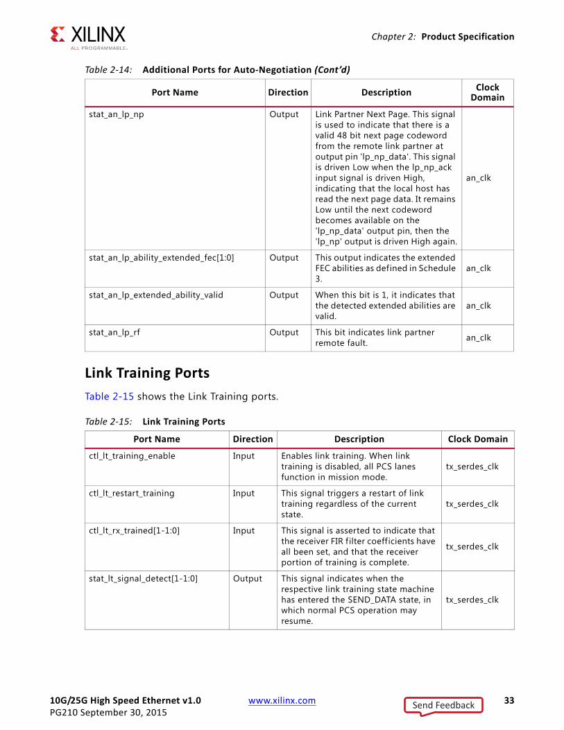
Auto‐Negotiation Ports
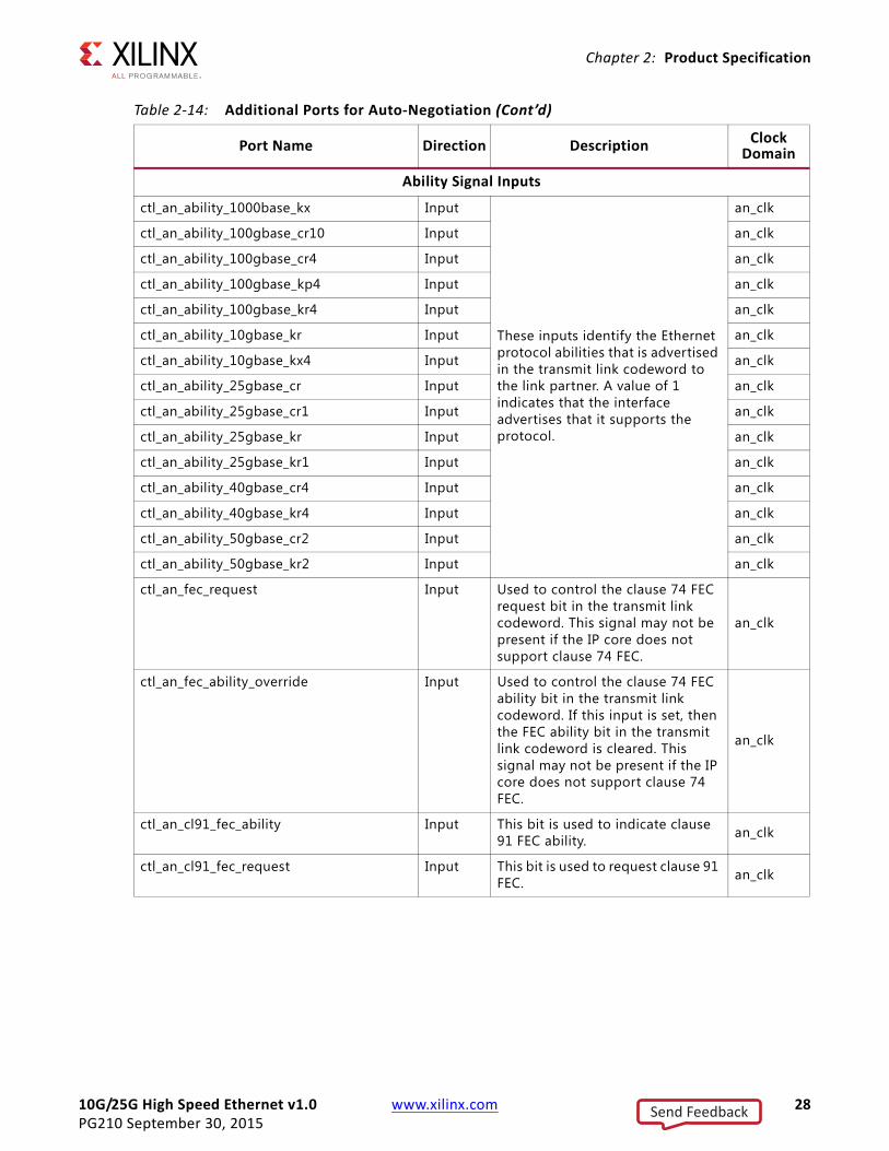
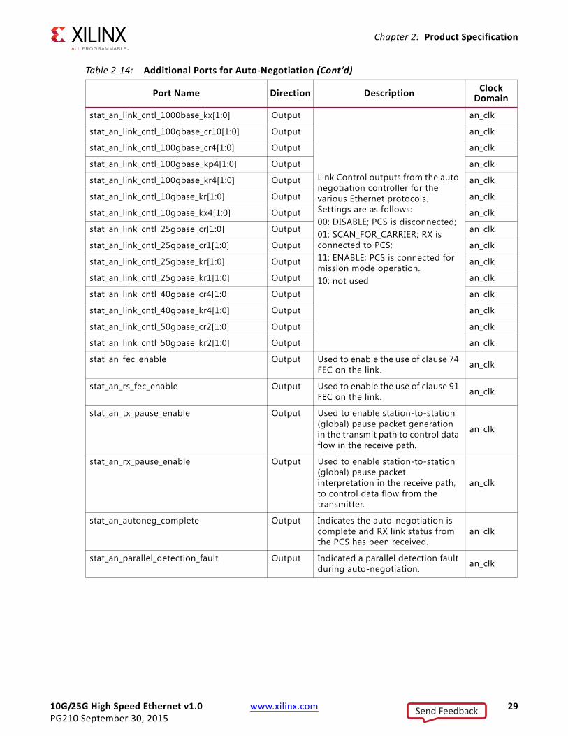
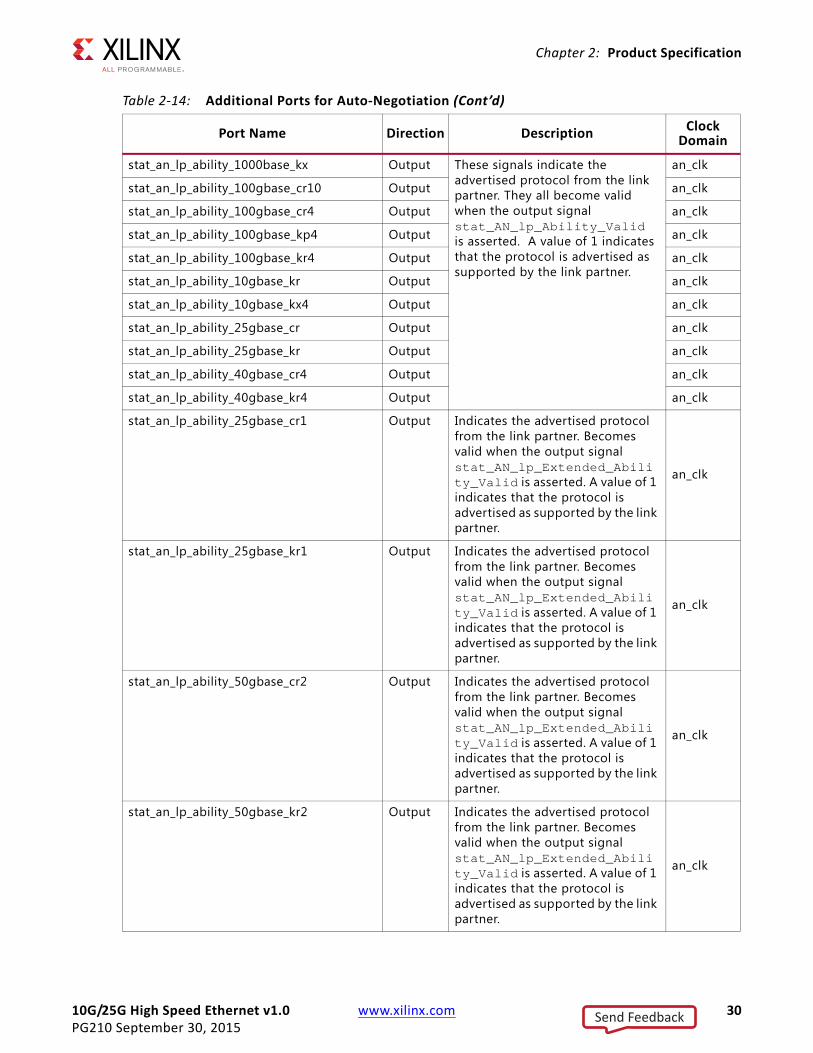
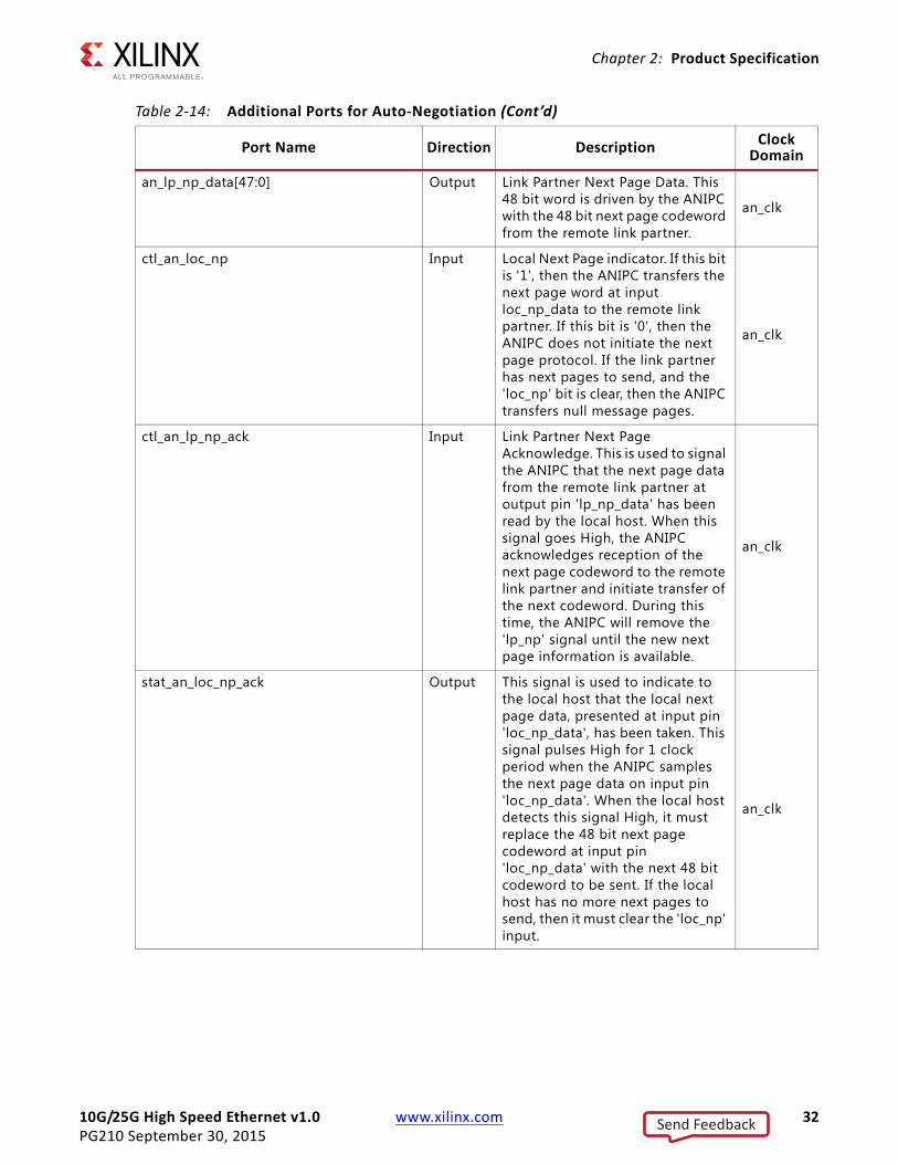
Table 2-14 shows the additional ports used for Auto-Negotiation. These signals are found at the *wrapper.v hierarchy f ile.
Table 2‐14: Additional Ports for Auto‐Negotiation
Port Name Direction Description Clock Domain
an_clk Input Input Clock for the auto-negotiation circuit. The required frequency is indicated in the readme file for the release.
Refer to Clocking.
an_reset Input Asynchronous active High reset. Asynch
ctl_autoneg_enable Input Enable signal for autonegotiation. an_clk
ctl_autoneg_bypass Input Input to disable autonegotiation and bypass the autonegotiation function. If this input is asserted, then autonegotiation is turned off, but the PCS is connected to the outputs to allow operation.
an_clk
ctl_an_nonce_seed[7:0] Input 8 bit seed to initialize the nonce f ield Polynomial generator. an_clk
ctl_an_pseudo_sel Input Selects the polynomial generator for the bit 49 random bit generator. If this input is 1, then the polynomial is x7+x6+1. If this input is zero, then the polynomial is x7+x3+1.
an_clk
ctl_restart_negotiation Input This input is used to trigger a restart of the auto negotiation, regardless of what state the circuit is currently in.
an_clk
ctl_an_local_fault Input This input signal is used to set the ‘local_fault’ bit of the transmit link codeword.
an_clk
Signals Used for Pause Ability Advertising
ctl_an_pause Input This input signal is used to set the ‘PAUSE’ bit, (C0), of the transmit link codeword. This signal may not be present if the core does not support pause.
an_clk
ctl_an_asmdir Input This input signal is used to set the ‘ASMDIR’ bit, (C1), of the transmit link codeword. This signal may not be present if the core does not support pause.
an_clk
Send Feedback
10G/25G High Speed Ethernet v1.0 www.xilinx.com 28PG210 September 30, 2015
Chapter 2: Product Specification
Ability Signal Inputs
ctl_an_ability_1000base_kx Input
These inputs identify the Ethernet protocol abilities that is advertised in the transmit link codeword to the link partner. A value of 1 indicates that the interface advertises that it supports the protocol.
an_clk
ctl_an_ability_100gbase_cr10 Input an_clk
ctl_an_ability_100gbase_cr4 Input an_clk
ctl_an_ability_100gbase_kp4 Input an_clk
ctl_an_ability_100gbase_kr4 Input an_clk
ctl_an_ability_10gbase_kr Input an_clk
ctl_an_ability_10gbase_kx4 Input an_clk
ctl_an_ability_25gbase_cr Input an_clk
ctl_an_ability_25gbase_cr1 Input an_clk
ctl_an_ability_25gbase_kr Input an_clk
ctl_an_ability_25gbase_kr1 Input an_clk
ctl_an_ability_40gbase_cr4 Input an_clk
ctl_an_ability_40gbase_kr4 Input an_clk
ctl_an_ability_50gbase_cr2 Input an_clk
ctl_an_ability_50gbase_kr2 Input an_clk
ctl_an_fec_request Input Used to control the clause 74 FEC request bit in the transmit link codeword. This signal may not be present if the IP core does not support clause 74 FEC.
an_clk
ctl_an_fec_ability_override Input Used to control the clause 74 FEC ability bit in the transmit link codeword. If this input is set, then the FEC ability bit in the transmit link codeword is cleared. This signal may not be present if the IP core does not support clause 74 FEC.
an_clk
ctl_an_cl91_fec_ability Input This bit is used to indicate clause 91 FEC ability. an_clk
ctl_an_cl91_fec_request Input This bit is used to request clause 91 FEC. an_clk
Table 2‐14: Additional Ports for Auto‐Negotiation (Cont’d)
Port Name Direction Description Clock Domain
Send Feedback
10G/25G High Speed Ethernet v1.0 www.xilinx.com 29PG210 September 30, 2015
Chapter 2: Product Specification
stat_an_link_cntl_1000base_kx[1:0] Output
Link Control outputs from the auto negotiation controller for the various Ethernet protocols. Settings are as follows: 00: DISABLE; PCS is disconnected;01: SCAN_FOR_CARRIER; RX is connected to PCS;11: ENABLE; PCS is connected for mission mode operation.10: not used
an_clk
stat_an_link_cntl_100gbase_cr10[1:0] Output an_clk
stat_an_link_cntl_100gbase_cr4[1:0] Output an_clk
stat_an_link_cntl_100gbase_kp4[1:0] Output an_clk
stat_an_link_cntl_100gbase_kr4[1:0] Output an_clk
stat_an_link_cntl_10gbase_kr[1:0] Output an_clk
stat_an_link_cntl_10gbase_kx4[1:0] Output an_clk
stat_an_link_cntl_25gbase_cr[1:0] Output an_clk
stat_an_link_cntl_25gbase_cr1[1:0] Output an_clk
stat_an_link_cntl_25gbase_kr[1:0] Output an_clk
stat_an_link_cntl_25gbase_kr1[1:0] Output an_clk
stat_an_link_cntl_40gbase_cr4[1:0] Output an_clk
stat_an_link_cntl_40gbase_kr4[1:0] Output an_clk
stat_an_link_cntl_50gbase_cr2[1:0] Output an_clk
stat_an_link_cntl_50gbase_kr2[1:0] Output an_clk
stat_an_fec_enable Output Used to enable the use of clause 74 FEC on the link. an_clk
stat_an_rs_fec_enable Output Used to enable the use of clause 91 FEC on the link. an_clk
stat_an_tx_pause_enable Output Used to enable station-to-station (global) pause packet generation in the transmit path to control data flow in the receive path.
an_clk
stat_an_rx_pause_enable Output Used to enable station-to-station (global) pause packet interpretation in the receive path, to control data flow from the transmitter.
an_clk
stat_an_autoneg_complete Output Indicates the auto-negotiation is complete and RX link status from the PCS has been received.
an_clk
stat_an_parallel_detection_fault Output Indicated a parallel detection fault during auto-negotiation. an_clk
Table 2‐14: Additional Ports for Auto‐Negotiation (Cont’d)
Port Name Direction Description Clock Domain
Send Feedback
10G/25G High Speed Ethernet v1.0 www.xilinx.com 30PG210 September 30, 2015
Chapter 2: Product Specification
stat_an_lp_ability_1000base_kx Output These signals indicate the advertised protocol from the link partner. They all become valid when the output signal stat_AN_lp_Ability_Valid is asserted. A value of 1 indicates that the protocol is advertised as supported by the link partner.
an_clk
stat_an_lp_ability_100gbase_cr10 Output an_clk
stat_an_lp_ability_100gbase_cr4 Output an_clk
stat_an_lp_ability_100gbase_kp4 Output an_clk
stat_an_lp_ability_100gbase_kr4 Output an_clk
stat_an_lp_ability_10gbase_kr Output an_clk
stat_an_lp_ability_10gbase_kx4 Output an_clk
stat_an_lp_ability_25gbase_cr Output an_clk
stat_an_lp_ability_25gbase_kr Output an_clk
stat_an_lp_ability_40gbase_cr4 Output an_clk
stat_an_lp_ability_40gbase_kr4 Output an_clk
stat_an_lp_ability_25gbase_cr1 Output Indicates the advertised protocol from the link partner. Becomes valid when the output signal stat_AN_lp_Extended_Ability_Valid is asserted. A value of 1 indicates that the protocol is advertised as supported by the link partner.
an_clk
stat_an_lp_ability_25gbase_kr1 Output Indicates the advertised protocol from the link partner. Becomes valid when the output signal stat_AN_lp_Extended_Ability_Valid is asserted. A value of 1 indicates that the protocol is advertised as supported by the link partner.
an_clk
stat_an_lp_ability_50gbase_cr2 Output Indicates the advertised protocol from the link partner. Becomes valid when the output signal stat_AN_lp_Extended_Ability_Valid is asserted. A value of 1 indicates that the protocol is advertised as supported by the link partner.
an_clk
stat_an_lp_ability_50gbase_kr2 Output Indicates the advertised protocol from the link partner. Becomes valid when the output signal stat_AN_lp_Extended_Ability_Valid is asserted. A value of 1 indicates that the protocol is advertised as supported by the link partner.
an_clk
Table 2‐14: Additional Ports for Auto‐Negotiation (Cont’d)
Port Name Direction Description Clock Domain
Send Feedback

10G/25G High Speed Ethernet v1.0 www.xilinx.com 31PG210 September 30, 2015
Chapter 2: Product Specification
stat_an_lp_pause Output This signal indicates the advertised value of the PAUSE bit, (C0), in the receive link codeword from the link partner. It becomes valid when the output signal stat_AN_lp_Ability_Valid is asserted.
an_clk
stat_an_lp_asm_dir Output This signal indicates the advertised value of the ASMDIR bit, (C1), in the receive link codeword from the link partner. It becomes valid when the output signal stat_AN_lp_Ability_Valid is asserted.
an_clk
stat_an_lp_fec_ability Output This signal indicates the advertised value of the FEC ability bit in the receive link codeword from the link partner. It becomes valid when the output signal stat_AN_lp_Ability_Valid is asserted.
an_clk
stat_an_lp_fec_request Output This signal indicates the advertised value of the FEC Request bit in the receive link codeword from the link partner. It becomes valid when the output signal stat_AN_lp_Ability_Valid is asserted.
an_clk
stat_an_lp_autoneg_able Output This output signal indicates that the link partner is able to perform autonegotiation. It becomes valid when the output signal stat_AN_lp_Ability_Valid is asserted.
an_clk
stat_an_lp_ability_valid Output This signal indicates when all of the link partner advertisements become valid.
an_clk
an_loc_np_data[47:0] Input Local Next Page codeword. This is the 48 bit codeword used if the 'loc_np' input is set. In this data f ield, the bits NP, ACK, and T, bit positions 15, 14, 12, & 11, are not transferred as part of the next page codeword. These bits are generated in the ANIPC. However, the Message Protocol bit, MP, in bit position 13, is transferred.
an_clk
Table 2‐14: Additional Ports for Auto‐Negotiation (Cont’d)
Port Name Direction Description Clock Domain
Send Feedback
10G/25G High Speed Ethernet v1.0 www.xilinx.com 32PG210 September 30, 2015
Chapter 2: Product Specification
an_lp_np_data[47:0] Output Link Partner Next Page Data. This 48 bit word is driven by the ANIPC with the 48 bit next page codeword from the remote link partner.
an_clk
ctl_an_loc_np Input Local Next Page indicator. If this bit is '1', then the ANIPC transfers the next page word at input loc_np_data to the remote link partner. If this bit is '0', then the ANIPC does not initiate the next page protocol. If the link partner has next pages to send, and the 'loc_np' bit is clear, then the ANIPC transfers null message pages.
an_clk
ctl_an_lp_np_ack Input Link Partner Next Page Acknowledge. This is used to signal the ANIPC that the next page data from the remote link partner at output pin 'lp_np_data' has been read by the local host. When this signal goes High, the ANIPC acknowledges reception of the next page codeword to the remote link partner and initiate transfer of the next codeword. During this time, the ANIPC will remove the 'lp_np' signal until the new next page information is available.
an_clk
stat_an_loc_np_ack Output This signal is used to indicate to the local host that the local next page data, presented at input pin 'loc_np_data', has been taken. This signal pulses High for 1 clock period when the ANIPC samples the next page data on input pin 'loc_np_data'. When the local host detects this signal High, it must replace the 48 bit next page codeword at input pin 'loc_np_data' with the next 48 bit codeword to be sent. If the local host has no more next pages to send, then it must clear the 'loc_np' input.
an_clk
Table 2‐14: Additional Ports for Auto‐Negotiation (Cont’d)
Port Name Direction Description Clock Domain
Send Feedback
10G/25G High Speed Ethernet v1.0 www.xilinx.com 33PG210 September 30, 2015
Chapter 2: Product Specification
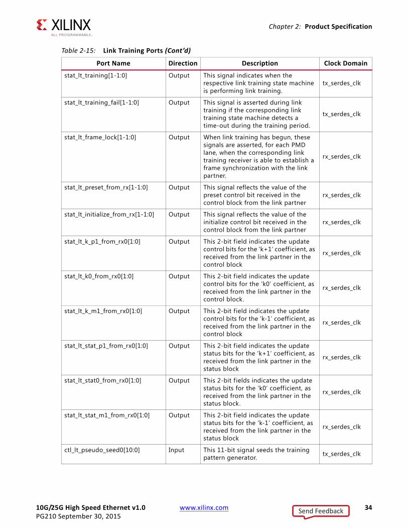
Link Training Ports
Table 2-15 shows the Link Training ports.
stat_an_lp_np Output Link Partner Next Page. This signal is used to indicate that there is a valid 48 bit next page codeword from the remote link partner at output pin 'lp_np_data'. This signal is driven Low when the lp_np_ack input signal is driven High, indicating that the local host has read the next page data. It remains Low until the next codeword becomes available on the 'lp_np_data' output pin, then the 'lp_np' output is driven High again.
an_clk
stat_an_lp_ability_extended_fec[1:0] Output This output indicates the extended FEC abilities as defined in Schedule 3.
an_clk
stat_an_lp_extended_ability_valid Output When this bit is 1, it indicates that the detected extended abilities are valid.
an_clk
stat_an_lp_rf Output This bit indicates link partner remote fault. an_clk
Table 2‐15: Link Training Ports
Port Name Direction Description Clock Domain
ctl_lt_training_enable Input Enables link training. When link training is disabled, all PCS lanes function in mission mode.
tx_serdes_clk
ctl_lt_restart_training Input This signal triggers a restart of link training regardless of the current state.
tx_serdes_clk
ctl_lt_rx_trained[1-1:0] Input This signal is asserted to indicate that the receiver FIR f ilter coefficients have all been set, and that the receiver portion of training is complete.
tx_serdes_clk
stat_lt_signal_detect[1-1:0] Output This signal indicates when the respective link training state machine has entered the SEND_DATA state, in which normal PCS operation may resume.
tx_serdes_clk
Table 2‐14: Additional Ports for Auto‐Negotiation (Cont’d)
Port Name Direction Description Clock Domain
Send Feedback
10G/25G High Speed Ethernet v1.0 www.xilinx.com 34PG210 September 30, 2015
Chapter 2: Product Specification
stat_lt_training[1-1:0] Output This signal indicates when the respective link training state machine is performing link training.
tx_serdes_clk
stat_lt_training_fail[1-1:0] Output This signal is asserted during link training if the corresponding link training state machine detects a time-out during the training period.
tx_serdes_clk
stat_lt_frame_lock[1-1:0] Output When link training has begun, these signals are asserted, for each PMD lane, when the corresponding link training receiver is able to establish a frame synchronization with the link partner.
rx_serdes_clk
stat_lt_preset_from_rx[1-1:0] Output This signal reflects the value of the preset control bit received in the control block from the link partner
rx_serdes_clk
stat_lt_initialize_from_rx[1-1:0] Output This signal reflects the value of the initialize control bit received in the control block from the link partner
rx_serdes_clk
stat_lt_k_p1_from_rx0[1:0] Output This 2-bit f ield indicates the update control bits for the ‘k+1’ coefficient, as received from the link partner in the control block
rx_serdes_clk
stat_lt_k0_from_rx0[1:0] Output This 2-bit f ield indicates the update control bits for the ‘k0’ coefficient, as received from the link partner in the control block.
rx_serdes_clk
stat_lt_k_m1_from_rx0[1:0] Output This 2-bit f ield indicates the update control bits for the ‘k-1’ coefficient, as received from the link partner in the control block
rx_serdes_clk
stat_lt_stat_p1_from_rx0[1:0] Output This 2-bit f ield indicates the update status bits for the ‘k+1’ coefficient, as received from the link partner in the status block
rx_serdes_clk
stat_lt_stat0_from_rx0[1:0] Output This 2-bit f ields indicates the update status bits for the ‘k0’ coeff icient, as received from the link partner in the status block.
rx_serdes_clk
stat_lt_stat_m1_from_rx0[1:0] Output This 2-bit f ield indicates the update status bits for the ‘k-1’ coefficient, as received from the link partner in the status block
rx_serdes_clk
ctl_lt_pseudo_seed0[10:0] Input This 11-bit signal seeds the training pattern generator. tx_serdes_clk
Table 2‐15: Link Training Ports (Cont’d)
Port Name Direction Description Clock Domain
Send Feedback
10G/25G High Speed Ethernet v1.0 www.xilinx.com 35PG210 September 30, 2015
Chapter 2: Product Specification
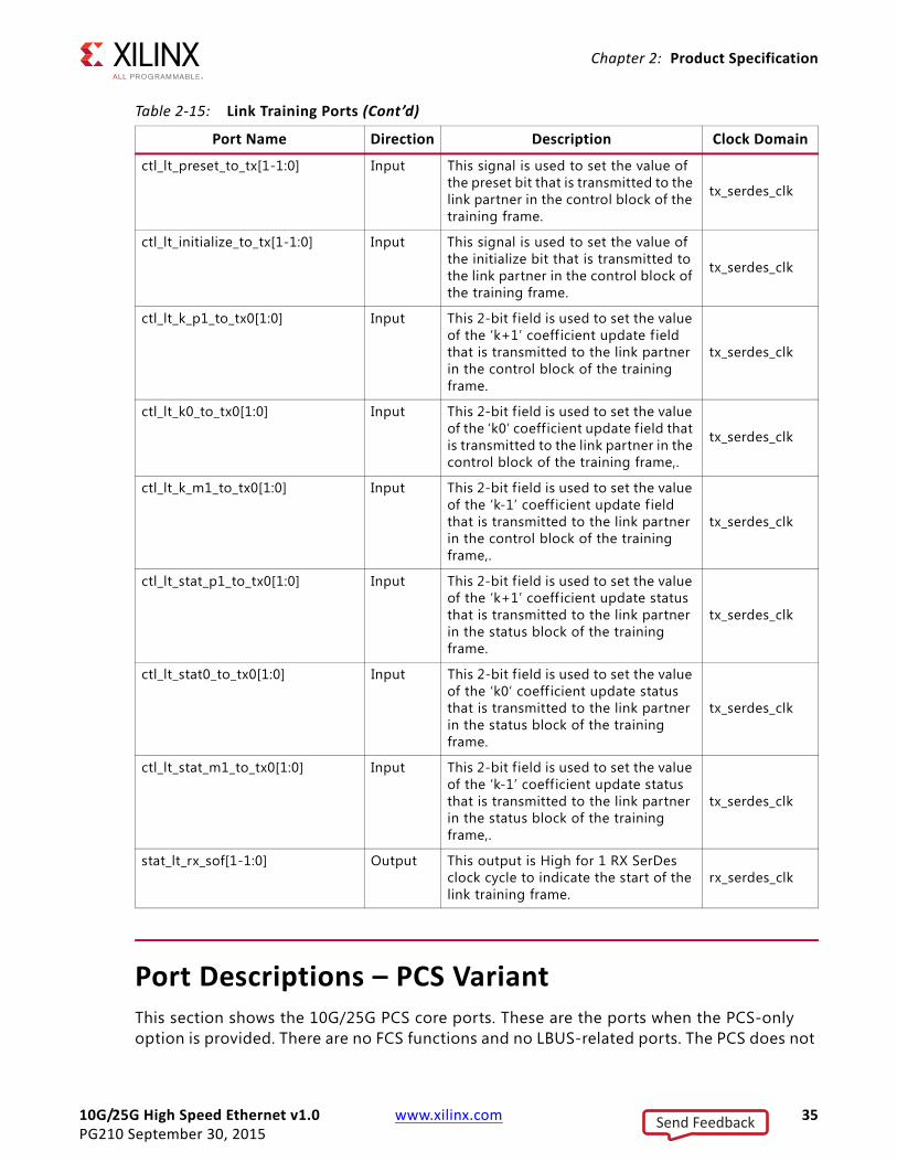
Port Descriptions – PCS VariantThis section shows the 10G/25G PCS core ports. These are the ports when the PCS-only option is provided. There are no FCS functions and no LBUS-related ports. The PCS does not
ctl_lt_preset_to_tx[1-1:0] Input This signal is used to set the value of the preset bit that is transmitted to the link partner in the control block of the training frame.
tx_serdes_clk
ctl_lt_initialize_to_tx[1-1:0] Input This signal is used to set the value of the initialize bit that is transmitted to the link partner in the control block of the training frame.
tx_serdes_clk
ctl_lt_k_p1_to_tx0[1:0] Input This 2-bit f ield is used to set the value of the ‘k+1’ coeff icient update f ield that is transmitted to the link partner in the control block of the training frame.
tx_serdes_clk
ctl_lt_k0_to_tx0[1:0] Input This 2-bit f ield is used to set the value of the ‘k0’ coefficient update field that is transmitted to the link partner in the control block of the training frame,.
tx_serdes_clk
ctl_lt_k_m1_to_tx0[1:0] Input This 2-bit f ield is used to set the value of the ‘k-1’ coefficient update f ield that is transmitted to the link partner in the control block of the training frame,.
tx_serdes_clk
ctl_lt_stat_p1_to_tx0[1:0] Input This 2-bit f ield is used to set the value of the ‘k+1’ coeff icient update status that is transmitted to the link partner in the status block of the training frame.
tx_serdes_clk
ctl_lt_stat0_to_tx0[1:0] Input This 2-bit f ield is used to set the value of the ‘k0’ coeff icient update status that is transmitted to the link partner in the status block of the training frame.
tx_serdes_clk
ctl_lt_stat_m1_to_tx0[1:0] Input This 2-bit f ield is used to set the value of the ‘k-1’ coefficient update status that is transmitted to the link partner in the status block of the training frame,.
tx_serdes_clk
stat_lt_rx_sof[1-1:0] Output This output is High for 1 RX SerDes clock cycle to indicate the start of the link training frame.
rx_serdes_clk
Table 2‐15: Link Training Ports (Cont’d)
Port Name Direction Description Clock Domain
Send Feedback
10G/25G High Speed Ethernet v1.0 www.xilinx.com 36PG210 September 30, 2015
Chapter 2: Product Specification
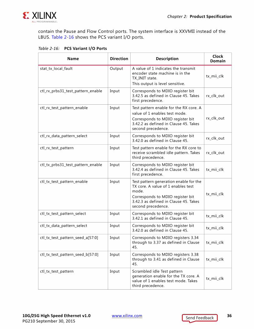
contain the Pause and Flow Control ports. The system interface is XXVMII instead of the LBUS. Table 2-16 shows the PCS variant I/O ports.
Table 2‐16: PCS Variant I/O Ports
Name Direction DescriptionClock
Domain
stat_tx_local_fault Output A value of 1 indicates the transmit encoder state machine is in the TX_INIT state.This output is level sensitive.
tx_mii_clk
ctl_rx_prbs31_test_pattern_enable Input Corresponds to MDIO register bit 3.42.5 as defined in Clause 45. Takes first precedence.
rx_clk_out
ctl_rx_test_pattern_enable Input Test pattern enable for the RX core. Avalue of 1 enables test mode.Corresponds to MDIO register bit 3.42.2 as defined in Clause 45. Takes second precedence.
rx_clk_out
ctl_rx_data_pattern_select Input Corresponds to MDIO register bit 3.42.0 as defined in Clause 45. rx_clk_out
ctl_rx_test_pattern Input Test pattern enable for the RX core to receive scrambled idle pattern. Takes third precedence.
rx_clk_out
ctl_tx_prbs31_test_pattern_enable Input Corresponds to MDIO register bit 3.42.4 as defined in Clause 45. Takes first precedence.
tx_mii_clk
ctl_tx_test_pattern_enable Input Test pattern generation enable for the TX core. A value of 1 enables test mode.Corresponds to MDIO register bit 3.42.3 as defined in Clause 45. Takes second precedence.
tx_mii_clk
ctl_tx_test_pattern_select Input Corresponds to MDIO register bit 3.42.1 as defined in Clause 45. tx_mii_clk
ctl_tx_data_pattern_select Input Corresponds to MDIO register bit 3.42.0 as defined in Clause 45. tx_mii_clk
ctl_tx_test_pattern_seed_a[57:0] Input Corresponds to MDIO registers 3.34 through to 3.37 as defined in Clause 45.
tx_mii_clk
ctl_tx_test_pattern_seed_b[57:0] Input Corresponds to MDIO registers 3.38 through to 3.41 as defined in Clause 45.
tx_mii_clk
ctl_tx_test_pattern Input Scrambled idle Test pattern generation enable for the TX core. A value of 1 enables test mode. Takes third precedence.
tx_mii_clk
Send Feedback
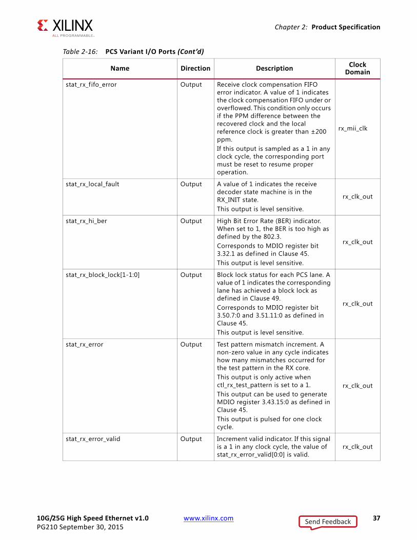
10G/25G High Speed Ethernet v1.0 www.xilinx.com 37PG210 September 30, 2015
Chapter 2: Product Specification
stat_rx_fifo_error Output Receive clock compensation FIFO error indicator. A value of 1 indicates the clock compensation FIFO under or overflowed. This condition only occurs if the PPM difference between the recovered clock and the local reference clock is greater than ±200 ppm.If this output is sampled as a 1 in any clock cycle, the corresponding port must be reset to resume proper operation.
rx_mii_clk
stat_rx_local_fault Output A value of 1 indicates the receive decoder state machine is in the RX_INIT state.This output is level sensitive.
rx_clk_out
stat_rx_hi_ber Output High Bit Error Rate (BER) indicator. When set to 1, the BER is too high as defined by the 802.3.Corresponds to MDIO register bit 3.32.1 as defined in Clause 45.This output is level sensitive.
rx_clk_out
stat_rx_block_lock[1-1:0] Output Block lock status for each PCS lane. A value of 1 indicates the corresponding lane has achieved a block lock as defined in Clause 49.Corresponds to MDIO register bit 3.50.7:0 and 3.51.11:0 as defined in Clause 45.This output is level sensitive.
rx_clk_out
stat_rx_error Output Test pattern mismatch increment. A non-zero value in any cycle indicates how many mismatches occurred for the test pattern in the RX core.This output is only active when ctl_rx_test_pattern is set to a 1.This output can be used to generate MDIO register 3.43.15:0 as defined in Clause 45.This output is pulsed for one clock cycle.
rx_clk_out
stat_rx_error_valid Output Increment valid indicator. If this signal is a 1 in any clock cycle, the value of stat_rx_error_valid[0:0] is valid.
rx_clk_out
Table 2‐16: PCS Variant I/O Ports (Cont’d)
Name Direction Description Clock Domain
Send Feedback
10G/25G High Speed Ethernet v1.0 www.xilinx.com 38PG210 September 30, 2015
Chapter 2: Product Specification
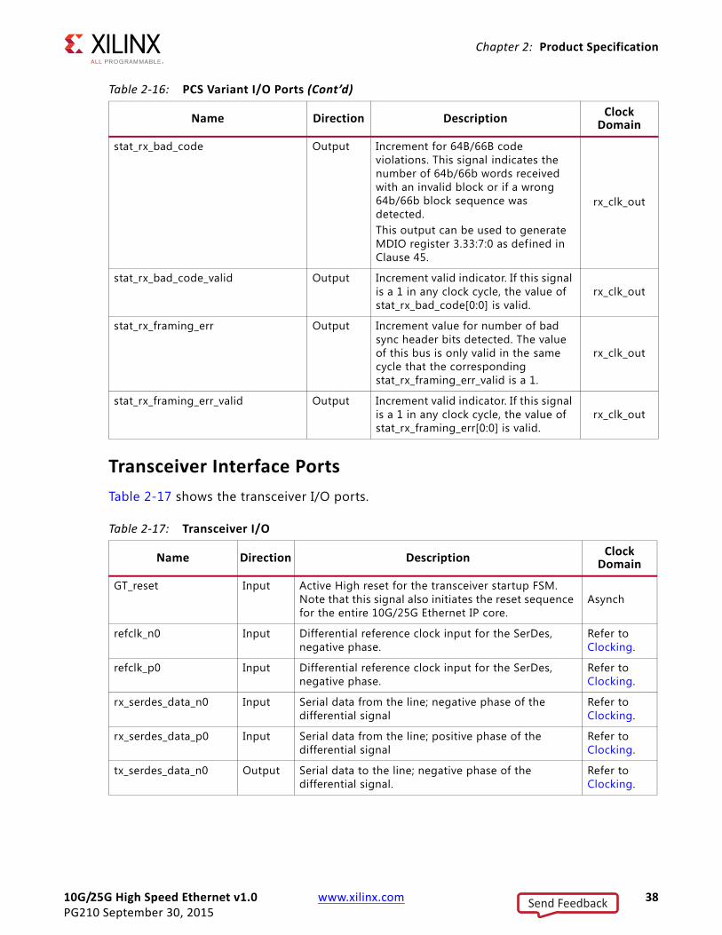
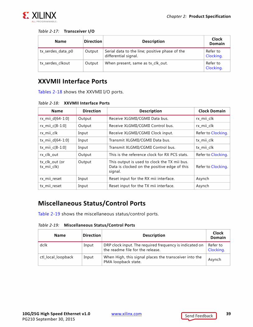
Transceiver Interface Ports
Table 2-17 shows the transceiver I/O ports.
stat_rx_bad_code Output Increment for 64B/66B code violations. This signal indicates the number of 64b/66b words received with an invalid block or if a wrong 64b/66b block sequence was detected.This output can be used to generate MDIO register 3.33:7:0 as defined in Clause 45.
rx_clk_out
stat_rx_bad_code_valid Output Increment valid indicator. If this signal is a 1 in any clock cycle, the value of stat_rx_bad_code[0:0] is valid.
rx_clk_out
stat_rx_framing_err Output Increment value for number of bad sync header bits detected. The value of this bus is only valid in the same cycle that the corresponding stat_rx_framing_err_valid is a 1.
rx_clk_out
stat_rx_framing_err_valid Output Increment valid indicator. If this signal is a 1 in any clock cycle, the value of stat_rx_framing_err[0:0] is valid.
rx_clk_out
Table 2‐17: Transceiver I/O
Name Direction DescriptionClock
Domain
GT_reset Input Active High reset for the transceiver startup FSM. Note that this signal also initiates the reset sequence for the entire 10G/25G Ethernet IP core.
Asynch
refclk_n0 Input Differential reference clock input for the SerDes, negative phase.
Refer to Clocking.
refclk_p0 Input Differential reference clock input for the SerDes, negative phase.
Refer to Clocking.
rx_serdes_data_n0 Input Serial data from the line; negative phase of the differential signal
Refer to Clocking.
rx_serdes_data_p0 Input Serial data from the line; positive phase of the differential signal
Refer to Clocking.
tx_serdes_data_n0 Output Serial data to the line; negative phase of the differential signal.
Refer to Clocking.
Table 2‐16: PCS Variant I/O Ports (Cont’d)
Name Direction Description Clock Domain
Send Feedback
10G/25G High Speed Ethernet v1.0 www.xilinx.com 39PG210 September 30, 2015
Chapter 2: Product Specification
XXVMII Interface Ports
Tables 2-18 shows the XXVMII I/O ports.
Miscellaneous Status/Control Ports
Table 2-19 shows the miscellaneous status/control ports.
tx_serdes_data_p0 Output Serial data to the line; positive phase of the differential signal.
Refer to Clocking.
tx_serdes_clkout Output When present, same as tx_clk_out. Refer to Clocking.
Table 2‐18: XXVMII Interface Ports
Name Direction Description Clock Domain
rx_mii_d[64-1:0] Output Receive XLGMII/CGMII Data bus. rx_mii_clk
rx_mii_c[8-1:0] Output Receive XLGMII/CGMII Control bus. rx_mii_clk
rx_mii_clk Input Receive XLGMII/CGMII Clock input. Refer to Clocking.
tx_mii_d[64-1:0] Input Transmit XLGMII/CGMII Data bus. tx_mii_clk
tx_mii_c[8-1:0] Input Transmit XLGMII/CGMII Control bus. tx_mii_clk
rx_clk_out Output This is the reference clock for RX PCS stats. Refer to Clocking.
tx_clk_out (or tx_mii_clk)
Output This output is used to clock the TX mii bus. Data is clocked on the positive edge of this signal.
Refer to Clocking.
rx_mii_reset Input Reset input for the RX mii interface. Asynch
tx_mii_reset Input Reset input for the TX mii interface. Asynch
Table 2‐19: Miscellaneous Status/Control Ports
Name Direction DescriptionClock
Domain
dclk Input DRP clock input. The required frequency is indicated on the readme file for the release.
Refer to Clocking.
ctl_local_loopback Input When High, this signal places the transceiver into the PMA loopback state. Asynch
Table 2‐17: Transceiver I/O
Name Direction Description Clock Domain
Send Feedback

10G/25G High Speed Ethernet v1.0 www.xilinx.com 40PG210 September 30, 2015
Chapter 2: Product Specification
Register Space
Register Descriptions
Configuration Register Map
This section contains descriptions of the configuration registers. In the cases where the features described in the bit f ields are not present in the IP core, the bit f ield reverts to RESERVED. Reserved f ields in the configuration registers do not accept any written value, and always return a 0 when read.
Table 2-20 describes the configuration registers for the 10G/25G Ethernet IP core. Registers or bit f ields within registers can be accessed for read-write (RW), write-only (WO), or read-only (RO). Default values shown are decimal values and take effect after reset. A description of each signal is found in the port list.
Table 2‐20: Configuration Register Map
Hex Address Register Name
0x0000 GT_RESET_REG
0x0004 RESET_REG
0x0008 MODE_REG
0x000C CONFIGURATION_TX_REG1
0x0014 CONFIGURATION_RX_REG1
0x0018 CONFIGURATION_RX_MTU
0x0020 TICK_REG
0x0024 CONFIGURATION_REVISION_REG
0x0028 CONFIGURATION_TX_TEST_PAT_SEED_A_LSB
0x002C CONFIGURATION_TX_TEST_PAT_SEED_A_MSB
0x0030 CONFIGURATION_TX_TEST_PAT_SEED_B_LSB
0x0034 CONFIGURATION_TX_TEST_PAT_SEED_B_MSB
0x0040 CONFIGURATION_TX_FLOW_CONTROL_REG1
0x0044 CONFIGURATION_TX_FLOW_CONTROL_REFRESH_REG1
0x0048 CONFIGURATION_TX_FLOW_CONTROL_REFRESH_REG2
0x004C CONFIGURATION_TX_FLOW_CONTROL_REFRESH_REG3
0x0050 CONFIGURATION_TX_FLOW_CONTROL_REFRESH_REG4
0x0054 CONFIGURATION_TX_FLOW_CONTROL_REFRESH_REG5
0x0058 CONFIGURATION_TX_FLOW_CONTROL_QUANTA_REG1
0x005C CONFIGURATION_TX_FLOW_CONTROL_QUANTA_REG2
Send Feedback

10G/25G High Speed Ethernet v1.0 www.xilinx.com 41PG210 September 30, 2015
Chapter 2: Product Specification
0x0060 CONFIGURATION_TX_FLOW_CONTROL_QUANTA_REG3
0x0064 CONFIGURATION_TX_FLOW_CONTROL_QUANTA_REG4
0x0068 CONFIGURATION_TX_FLOW_CONTROL_QUANTA_REG5
0x006C CONFIGURATION_TX_FLOW_CONTROL_PPP_ETYPE_OP_REG
0x0070 CONFIGURATION_TX_FLOW_CONTROL_GPP_ETYPE_OP_REG
0x0074 CONFIGURATION_TX_FLOW_CONTROL_GPP_DA_REG_LSB
0x0078 CONFIGURATION_TX_FLOW_CONTROL_GPP_DA_REG_MSB
0x007C CONFIGURATION_TX_FLOW_CONTROL_GPP_SA_REG_LSB
0x0080 CONFIGURATION_TX_FLOW_CONTROL_GPP_SA_REG_MSB
0x0084 CONFIGURATION_TX_FLOW_CONTROL_PPP_DA_REG_LSB
0x0088 CONFIGURATION_TX_FLOW_CONTROL_PPP_DA_REG_MSB
0x008C CONFIGURATION_TX_FLOW_CONTROL_PPP_SA_REG_LSB
0x0090 CONFIGURATION_TX_FLOW_CONTROL_PPP_SA_REG_MSB
0x0094 CONFIGURATION_RX_FLOW_CONTROL_REG1
0x0098 CONFIGURATION_RX_FLOW_CONTROL_REG2
0x009C CONFIGURATION_RX_FLOW_CONTROL_PPP_ETYPE_OP_REG
0x00A0 CONFIGURATION_RX_FLOW_CONTROL_GPP_ETYPE_OP_REG
0x00A4 CONFIGURATION_RX_FLOW_CONTROL_GCP_PCP_TYPE_REG
0x00A8 CONFIGURATION_RX_FLOW_CONTROL_PCP_OP_REG
0x00AC CONFIGURATION_RX_FLOW_CONTROL_GCP_OP_REG
0x00B0 CONFIGURATION_RX_FLOW_CONTROL_DA_REG1_LSB
0x00B4 CONFIGURATION_RX_FLOW_CONTROL_DA_REG1_MSB
0x00B8 CONFIGURATION_RX_FLOW_CONTROL_DA_REG2_LSB
0x00BC CONFIGURATION_RX_FLOW_CONTROL_DA_REG2_MSB
0x00C0 CONFIGURATION_RX_FLOW_CONTROL_SA_REG1_LSB
0x00C4 CONFIGURATION_RX_FLOW_CONTROL_SA_REG1_MSB
0x00D4 CONFIGURATION_FEC_REG
0x00E0 CONFIGURATION_AN_CONTROL_REG1
0x00E4 CONFIGURATION_AN_CONTROL_REG2
0x00F8 CONFIGURATION_AN_ABILITY
0x0100 CONFIGURATION_LT_CONTROL_REG1
0x0104 CONFIGURATION_LT_TRAINED_REG
0x0108 CONFIGURATION_LT_PRESET_REG
0x010C CONFIGURATION_LT_INIT_REG
Table 2‐20: Configuration Register Map (Cont’d)
Hex Address Register Name
Send Feedback
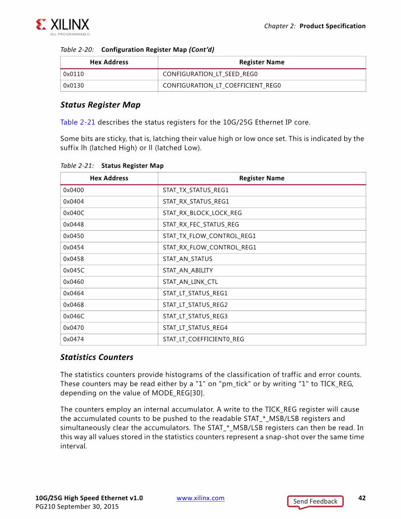
10G/25G High Speed Ethernet v1.0 www.xilinx.com 42PG210 September 30, 2015
Chapter 2: Product Specification
Status Register Map
Table 2-21 describes the status registers for the 10G/25G Ethernet IP core.
Some bits are sticky, that is, latching their value high or low once set. This is indicated by the suff ix lh (latched High) or ll (latched Low).
Statistics Counters
The statistics counters provide histograms of the classif ication of traff ic and error counts. These counters may be read either by a "1" on "pm_tick" or by writing "1" to TICK_REG, depending on the value of MODE_REG[30].
The counters employ an internal accumulator. A write to the TICK_REG register will cause the accumulated counts to be pushed to the readable STAT_*_MSB/LSB registers and simultaneously clear the accumulators. The STAT_*_MSB/LSB registers can then be read. In this way all values stored in the statistics counters represent a snap-shot over the same time interval.
0x0110 CONFIGURATION_LT_SEED_REG0
0x0130 CONFIGURATION_LT_COEFFICIENT_REG0
Table 2‐21: Status Register Map
Hex Address Register Name
0x0400 STAT_TX_STATUS_REG1
0x0404 STAT_RX_STATUS_REG1
0x040C STAT_RX_BLOCK_LOCK_REG
0x0448 STAT_RX_FEC_STATUS_REG
0x0450 STAT_TX_FLOW_CONTROL_REG1
0x0454 STAT_RX_FLOW_CONTROL_REG1
0x0458 STAT_AN_STATUS
0x045C STAT_AN_ABILITY
0x0460 STAT_AN_LINK_CTL
0x0464 STAT_LT_STATUS_REG1
0x0468 STAT_LT_STATUS_REG2
0x046C STAT_LT_STATUS_REG3
0x0470 STAT_LT_STATUS_REG4
0x0474 STAT_LT_COEFFICIENT0_REG
Table 2‐20: Configuration Register Map (Cont’d)
Hex Address Register Name
Send Feedback
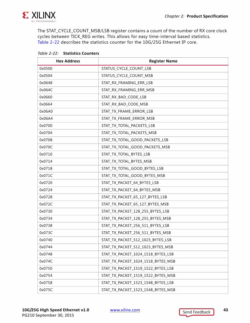
10G/25G High Speed Ethernet v1.0 www.xilinx.com 43PG210 September 30, 2015
Chapter 2: Product Specification
The STAT_CYCLE_COUNT_MSB/LSB register contains a count of the number of RX core clock cycles between TICK_REG writes. This allows for easy time-interval based statistics. Table 2-22 describes the statistics counter for the 10G/25G Ethernet IP core.
Table 2‐22: Statistics Counters
Hex Address Register Name
0x0500 STATUS_CYCLE_COUNT_LSB
0x0504 STATUS_CYCLE_COUNT_MSB
0x0648 STAT_RX_FRAMING_ERR_LSB
0x064C STAT_RX_FRAMING_ERR_MSB
0x0660 STAT_RX_BAD_CODE_LSB
0x0664 STAT_RX_BAD_CODE_MSB
0x06A0 STAT_TX_FRAME_ERROR_LSB
0x06A4 STAT_TX_FRAME_ERROR_MSB
0x0700 STAT_TX_TOTAL_PACKETS_LSB
0x0704 STAT_TX_TOTAL_PACKETS_MSB
0x0708 STAT_TX_TOTAL_GOOD_PACKETS_LSB
0x070C STAT_TX_TOTAL_GOOD_PACKETS_MSB
0x0710 STAT_TX_TOTAL_BYTES_LSB
0x0714 STAT_TX_TOTAL_BYTES_MSB
0x0718 STAT_TX_TOTAL_GOOD_BYTES_LSB
0x071C STAT_TX_TOTAL_GOOD_BYTES_MSB
0x0720 STAT_TX_PACKET_64_BYTES_LSB
0x0724 STAT_TX_PACKET_64_BYTES_MSB
0x0728 STAT_TX_PACKET_65_127_BYTES_LSB
0x072C STAT_TX_PACKET_65_127_BYTES_MSB
0x0730 STAT_TX_PACKET_128_255_BYTES_LSB
0x0734 STAT_TX_PACKET_128_255_BYTES_MSB
0x0738 STAT_TX_PACKET_256_511_BYTES_LSB
0x073C STAT_TX_PACKET_256_511_BYTES_MSB
0x0740 STAT_TX_PACKET_512_1023_BYTES_LSB
0x0744 STAT_TX_PACKET_512_1023_BYTES_MSB
0x0748 STAT_TX_PACKET_1024_1518_BYTES_LSB
0x074C STAT_TX_PACKET_1024_1518_BYTES_MSB
0x0750 STAT_TX_PACKET_1519_1522_BYTES_LSB
0x0754 STAT_TX_PACKET_1519_1522_BYTES_MSB
0x0758 STAT_TX_PACKET_1523_1548_BYTES_LSB
0x075C STAT_TX_PACKET_1523_1548_BYTES_MSB
Send Feedback

10G/25G High Speed Ethernet v1.0 www.xilinx.com 44PG210 September 30, 2015
Chapter 2: Product Specification
0x0760 STAT_TX_PACKET_1549_2047_BYTES_LSB
0x0764 STAT_TX_PACKET_1549_2047_BYTES_MSB
0x0768 STAT_TX_PACKET_2048_4095_BYTES_LSB
0x076C STAT_TX_PACKET_2048_4095_BYTES_MSB
0x0770 STAT_TX_PACKET_4096_8191_BYTES_LSB
0x0774 STAT_TX_PACKET_4096_8191_BYTES_MSB
0x0778 STAT_TX_PACKET_8192_9215_BYTES_LSB
0x077C STAT_TX_PACKET_8192_9215_BYTES_MSB
0x0780 STAT_TX_PACKET_LARGE_LSB
0x0784 STAT_TX_PACKET_LARGE_MSB
0x0788 STAT_TX_PACKET_SMALL_LSB
0x078C STAT_TX_PACKET_SMALL_MSB
0x07B8 STAT_TX_BAD_FCS_LSB
0x07BC STAT_TX_BAD_FCS_MSB
0x07D0 STAT_TX_UNICAST_LSB
0x07D4 STAT_TX_UNICAST_MSB
0x07D8 STAT_TX_MULTICAST_LSB
0x07DC STAT_TX_MULTICAST_MSB
0x07E0 STAT_TX_BROADCAST_LSB
0x07E4 STAT_TX_BROADCAST_MSB
0x07E8 STAT_TX_VLAN_LSB
0x07EC STAT_TX_VLAN_MSB
0x07F0 STAT_TX_PAUSE_LSB
0x07F4 STAT_TX_PAUSE_MSB
0x07F8 STAT_TX_USER_PAUSE_LSB
0x07FC STAT_TX_USER_PAUSE_MSB
0x0808 STAT_RX_TOTAL_PACKETS_LSB
0x080C STAT_RX_TOTAL_PACKETS_MSB
0x0810 STAT_RX_TOTAL_GOOD_PACKETS_LSB
0x0814 STAT_RX_TOTAL_GOOD_PACKETS_MSB
0x0818 STAT_RX_TOTAL_BYTES_LSB
0x081C STAT_RX_TOTAL_BYTES_MSB
0x0820 STAT_RX_TOTAL_GOOD_BYTES_LSB
0x0824 STAT_RX_TOTAL_GOOD_BYTES_MSB
0x0828 STAT_RX_PACKET_64_BYTES_LSB
Table 2‐22: Statistics Counters (Cont’d)
Hex Address Register Name
Send Feedback
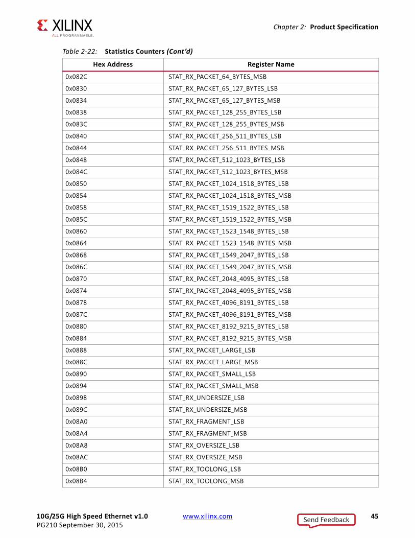
10G/25G High Speed Ethernet v1.0 www.xilinx.com 45PG210 September 30, 2015
Chapter 2: Product Specification
0x082C STAT_RX_PACKET_64_BYTES_MSB
0x0830 STAT_RX_PACKET_65_127_BYTES_LSB
0x0834 STAT_RX_PACKET_65_127_BYTES_MSB
0x0838 STAT_RX_PACKET_128_255_BYTES_LSB
0x083C STAT_RX_PACKET_128_255_BYTES_MSB
0x0840 STAT_RX_PACKET_256_511_BYTES_LSB
0x0844 STAT_RX_PACKET_256_511_BYTES_MSB
0x0848 STAT_RX_PACKET_512_1023_BYTES_LSB
0x084C STAT_RX_PACKET_512_1023_BYTES_MSB
0x0850 STAT_RX_PACKET_1024_1518_BYTES_LSB
0x0854 STAT_RX_PACKET_1024_1518_BYTES_MSB
0x0858 STAT_RX_PACKET_1519_1522_BYTES_LSB
0x085C STAT_RX_PACKET_1519_1522_BYTES_MSB
0x0860 STAT_RX_PACKET_1523_1548_BYTES_LSB
0x0864 STAT_RX_PACKET_1523_1548_BYTES_MSB
0x0868 STAT_RX_PACKET_1549_2047_BYTES_LSB
0x086C STAT_RX_PACKET_1549_2047_BYTES_MSB
0x0870 STAT_RX_PACKET_2048_4095_BYTES_LSB
0x0874 STAT_RX_PACKET_2048_4095_BYTES_MSB
0x0878 STAT_RX_PACKET_4096_8191_BYTES_LSB
0x087C STAT_RX_PACKET_4096_8191_BYTES_MSB
0x0880 STAT_RX_PACKET_8192_9215_BYTES_LSB
0x0884 STAT_RX_PACKET_8192_9215_BYTES_MSB
0x0888 STAT_RX_PACKET_LARGE_LSB
0x088C STAT_RX_PACKET_LARGE_MSB
0x0890 STAT_RX_PACKET_SMALL_LSB
0x0894 STAT_RX_PACKET_SMALL_MSB
0x0898 STAT_RX_UNDERSIZE_LSB
0x089C STAT_RX_UNDERSIZE_MSB
0x08A0 STAT_RX_FRAGMENT_LSB
0x08A4 STAT_RX_FRAGMENT_MSB
0x08A8 STAT_RX_OVERSIZE_LSB
0x08AC STAT_RX_OVERSIZE_MSB
0x08B0 STAT_RX_TOOLONG_LSB
0x08B4 STAT_RX_TOOLONG_MSB
Table 2‐22: Statistics Counters (Cont’d)
Hex Address Register Name
Send Feedback
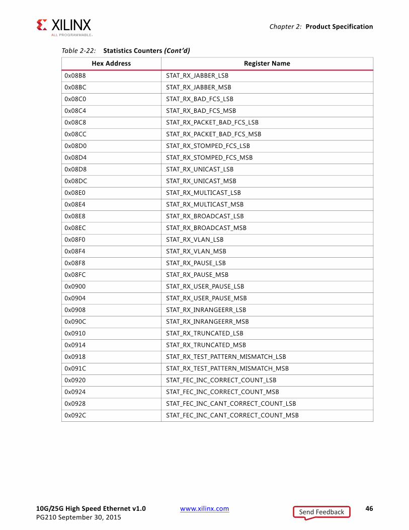
10G/25G High Speed Ethernet v1.0 www.xilinx.com 46PG210 September 30, 2015
Chapter 2: Product Specification
0x08B8 STAT_RX_JABBER_LSB
0x08BC STAT_RX_JABBER_MSB
0x08C0 STAT_RX_BAD_FCS_LSB
0x08C4 STAT_RX_BAD_FCS_MSB
0x08C8 STAT_RX_PACKET_BAD_FCS_LSB
0x08CC STAT_RX_PACKET_BAD_FCS_MSB
0x08D0 STAT_RX_STOMPED_FCS_LSB
0x08D4 STAT_RX_STOMPED_FCS_MSB
0x08D8 STAT_RX_UNICAST_LSB
0x08DC STAT_RX_UNICAST_MSB
0x08E0 STAT_RX_MULTICAST_LSB
0x08E4 STAT_RX_MULTICAST_MSB
0x08E8 STAT_RX_BROADCAST_LSB
0x08EC STAT_RX_BROADCAST_MSB
0x08F0 STAT_RX_VLAN_LSB
0x08F4 STAT_RX_VLAN_MSB
0x08F8 STAT_RX_PAUSE_LSB
0x08FC STAT_RX_PAUSE_MSB
0x0900 STAT_RX_USER_PAUSE_LSB
0x0904 STAT_RX_USER_PAUSE_MSB
0x0908 STAT_RX_INRANGEERR_LSB
0x090C STAT_RX_INRANGEERR_MSB
0x0910 STAT_RX_TRUNCATED_LSB
0x0914 STAT_RX_TRUNCATED_MSB
0x0918 STAT_RX_TEST_PATTERN_MISMATCH_LSB
0x091C STAT_RX_TEST_PATTERN_MISMATCH_MSB
0x0920 STAT_FEC_INC_CORRECT_COUNT_LSB
0x0924 STAT_FEC_INC_CORRECT_COUNT_MSB
0x0928 STAT_FEC_INC_CANT_CORRECT_COUNT_LSB
0x092C STAT_FEC_INC_CANT_CORRECT_COUNT_MSB
Table 2‐22: Statistics Counters (Cont’d)
Hex Address Register Name
Send Feedback
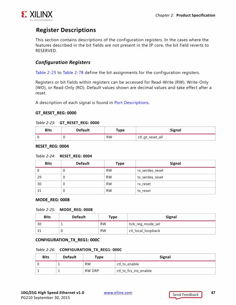
10G/25G High Speed Ethernet v1.0 www.xilinx.com 47PG210 September 30, 2015
Chapter 2: Product Specification
Register Descriptions
This section contains descriptions of the configuration registers. In the cases where the features described in the bit f ields are not present in the IP core, the bit f ield reverts to RESERVED.
Configuration Registers
Table 2-23 to Table 2-78 define the bit assignments for the configuration registers.
Registers or bit f ields within registers can be accessed for Read-Write (RW), Write-Only (WO), or Read-Only (RO). Default values shown are decimal values and take effect after a reset.
A description of each signal is found in Port Descriptions.
GT_RESET_REG: 0000
RESET_REG: 0004
MODE_REG: 0008
CONFIGURATION_TX_REG1: 000C
Table 2‐23: GT_RESET_REG: 0000
Bits Default Type Signal
0 0 RW ctl_gt_reset_all
Table 2‐24: RESET_REG: 0004
Bits Default Type Signal
0 0 RW rx_serdes_reset
29 0 RW tx_serdes_reset
30 0 RW rx_reset
31 0 RW tx_reset
Table 2‐25: MODE_REG: 0008
Bits Default Type Signal
30 1 RW tick_reg_mode_sel
31 0 RW ctl_local_loopback
Table 2‐26: CONFIGURATION_TX_REG1: 000C
Bits Default Type Signal
0 1 RW ctl_tx_enable
1 1 RW DRP ctl_tx_fcs_ins_enable
Send Feedback
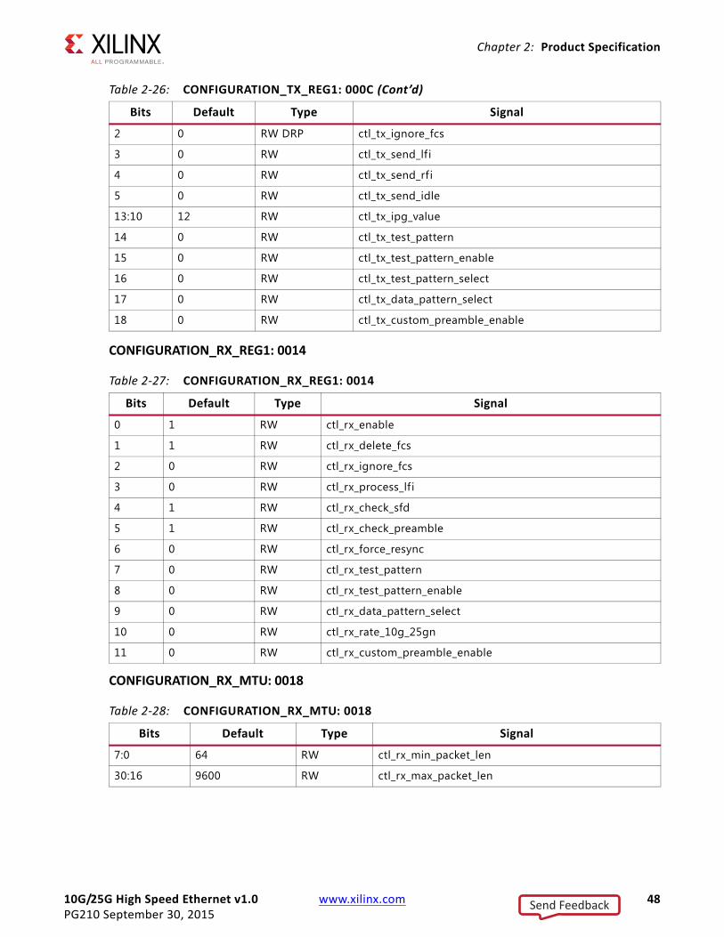
10G/25G High Speed Ethernet v1.0 www.xilinx.com 48PG210 September 30, 2015
Chapter 2: Product Specification
CONFIGURATION_RX_REG1: 0014
CONFIGURATION_RX_MTU: 0018
2 0 RW DRP ctl_tx_ignore_fcs
3 0 RW ctl_tx_send_lf i
4 0 RW ctl_tx_send_rf i
5 0 RW ctl_tx_send_idle
13:10 12 RW ctl_tx_ipg_value
14 0 RW ctl_tx_test_pattern
15 0 RW ctl_tx_test_pattern_enable
16 0 RW ctl_tx_test_pattern_select
17 0 RW ctl_tx_data_pattern_select
18 0 RW ctl_tx_custom_preamble_enable
Table 2‐27: CONFIGURATION_RX_REG1: 0014
Bits Default Type Signal
0 1 RW ctl_rx_enable
1 1 RW ctl_rx_delete_fcs
2 0 RW ctl_rx_ignore_fcs
3 0 RW ctl_rx_process_lf i
4 1 RW ctl_rx_check_sfd
5 1 RW ctl_rx_check_preamble
6 0 RW ctl_rx_force_resync
7 0 RW ctl_rx_test_pattern
8 0 RW ctl_rx_test_pattern_enable
9 0 RW ctl_rx_data_pattern_select
10 0 RW ctl_rx_rate_10g_25gn
11 0 RW ctl_rx_custom_preamble_enable
Table 2‐28: CONFIGURATION_RX_MTU: 0018
Bits Default Type Signal
7:0 64 RW ctl_rx_min_packet_len
30:16 9600 RW ctl_rx_max_packet_len
Table 2‐26: CONFIGURATION_TX_REG1: 000C (Cont’d)
Bits Default Type Signal
Send Feedback
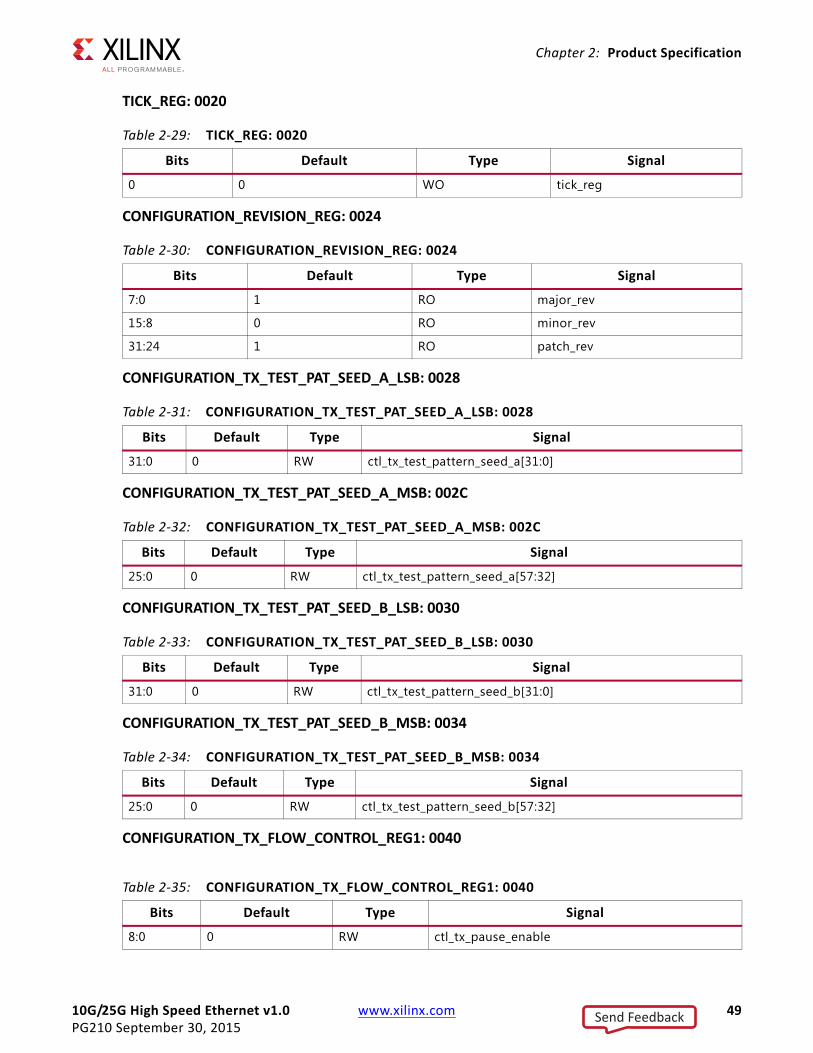
10G/25G High Speed Ethernet v1.0 www.xilinx.com 49PG210 September 30, 2015
Chapter 2: Product Specification
TICK_REG: 0020
CONFIGURATION_REVISION_REG: 0024
CONFIGURATION_TX_TEST_PAT_SEED_A_LSB: 0028
CONFIGURATION_TX_TEST_PAT_SEED_A_MSB: 002C
CONFIGURATION_TX_TEST_PAT_SEED_B_LSB: 0030
CONFIGURATION_TX_TEST_PAT_SEED_B_MSB: 0034
CONFIGURATION_TX_FLOW_CONTROL_REG1: 0040
Table 2‐29: TICK_REG: 0020
Bits Default Type Signal
0 0 WO tick_reg
Table 2‐30: CONFIGURATION_REVISION_REG: 0024
Bits Default Type Signal
7:0 1 RO major_rev
15:8 0 RO minor_rev
31:24 1 RO patch_rev
Table 2‐31: CONFIGURATION_TX_TEST_PAT_SEED_A_LSB: 0028
Bits Default Type Signal
31:0 0 RW ctl_tx_test_pattern_seed_a[31:0]
Table 2‐32: CONFIGURATION_TX_TEST_PAT_SEED_A_MSB: 002C
Bits Default Type Signal
25:0 0 RW ctl_tx_test_pattern_seed_a[57:32]
Table 2‐33: CONFIGURATION_TX_TEST_PAT_SEED_B_LSB: 0030
Bits Default Type Signal
31:0 0 RW ctl_tx_test_pattern_seed_b[31:0]
Table 2‐34: CONFIGURATION_TX_TEST_PAT_SEED_B_MSB: 0034
Bits Default Type Signal
25:0 0 RW ctl_tx_test_pattern_seed_b[57:32]
Table 2‐35: CONFIGURATION_TX_FLOW_CONTROL_REG1: 0040
Bits Default Type Signal
8:0 0 RW ctl_tx_pause_enable
Send Feedback
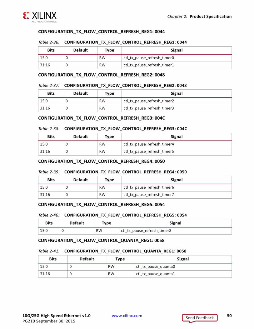
10G/25G High Speed Ethernet v1.0 www.xilinx.com 50PG210 September 30, 2015
Chapter 2: Product Specification
CONFIGURATION_TX_FLOW_CONTROL_REFRESH_REG1: 0044
CONFIGURATION_TX_FLOW_CONTROL_REFRESH_REG2: 0048
CONFIGURATION_TX_FLOW_CONTROL_REFRESH_REG3: 004C
CONFIGURATION_TX_FLOW_CONTROL_REFRESH_REG4: 0050
CONFIGURATION_TX_FLOW_CONTROL_REFRESH_REG5: 0054
CONFIGURATION_TX_FLOW_CONTROL_QUANTA_REG1: 0058
Table 2‐36: CONFIGURATION_TX_FLOW_CONTROL_REFRESH_REG1: 0044
Bits Default Type Signal
15:0 0 RW ctl_tx_pause_refresh_timer0
31:16 0 RW ctl_tx_pause_refresh_timer1
Table 2‐37: CONFIGURATION_TX_FLOW_CONTROL_REFRESH_REG2: 0048
Bits Default Type Signal
15:0 0 RW ctl_tx_pause_refresh_timer2
31:16 0 RW ctl_tx_pause_refresh_timer3
Table 2‐38: CONFIGURATION_TX_FLOW_CONTROL_REFRESH_REG3: 004C
Bits Default Type Signal
15:0 0 RW ctl_tx_pause_refresh_timer4
31:16 0 RW ctl_tx_pause_refresh_timer5
Table 2‐39: CONFIGURATION_TX_FLOW_CONTROL_REFRESH_REG4: 0050
Bits Default Type Signal
15:0 0 RW ctl_tx_pause_refresh_timer6
31:16 0 RW ctl_tx_pause_refresh_timer7
Table 2‐40: CONFIGURATION_TX_FLOW_CONTROL_REFRESH_REG5: 0054
Bits Default Type Signal
15:0 0 RW ctl_tx_pause_refresh_timer8
Table 2‐41: CONFIGURATION_TX_FLOW_CONTROL_QUANTA_REG1: 0058
Bits Default Type Signal
15:0 0 RW ctl_tx_pause_quanta0
31:16 0 RW ctl_tx_pause_quanta1
Send Feedback
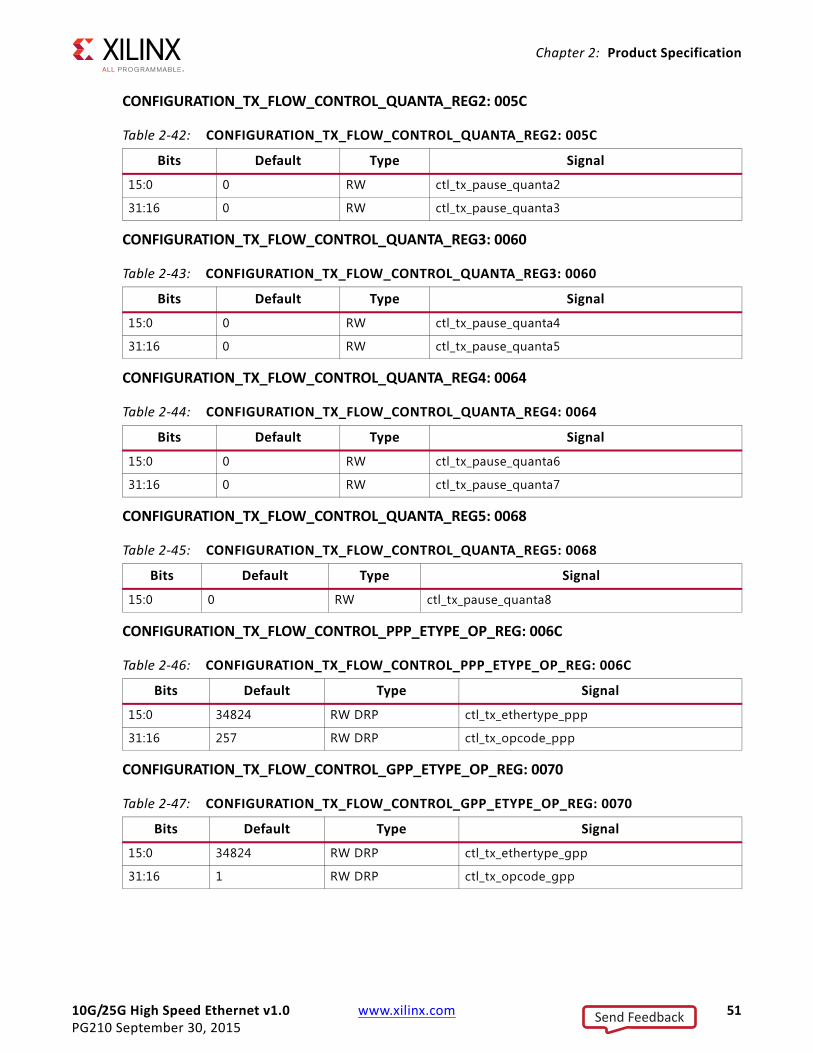
10G/25G High Speed Ethernet v1.0 www.xilinx.com 51PG210 September 30, 2015
Chapter 2: Product Specification
CONFIGURATION_TX_FLOW_CONTROL_QUANTA_REG2: 005C
CONFIGURATION_TX_FLOW_CONTROL_QUANTA_REG3: 0060
CONFIGURATION_TX_FLOW_CONTROL_QUANTA_REG4: 0064
CONFIGURATION_TX_FLOW_CONTROL_QUANTA_REG5: 0068
CONFIGURATION_TX_FLOW_CONTROL_PPP_ETYPE_OP_REG: 006C
CONFIGURATION_TX_FLOW_CONTROL_GPP_ETYPE_OP_REG: 0070
Table 2‐42: CONFIGURATION_TX_FLOW_CONTROL_QUANTA_REG2: 005C
Bits Default Type Signal
15:0 0 RW ctl_tx_pause_quanta2
31:16 0 RW ctl_tx_pause_quanta3
Table 2‐43: CONFIGURATION_TX_FLOW_CONTROL_QUANTA_REG3: 0060
Bits Default Type Signal
15:0 0 RW ctl_tx_pause_quanta4
31:16 0 RW ctl_tx_pause_quanta5
Table 2‐44: CONFIGURATION_TX_FLOW_CONTROL_QUANTA_REG4: 0064
Bits Default Type Signal
15:0 0 RW ctl_tx_pause_quanta6
31:16 0 RW ctl_tx_pause_quanta7
Table 2‐45: CONFIGURATION_TX_FLOW_CONTROL_QUANTA_REG5: 0068
Bits Default Type Signal
15:0 0 RW ctl_tx_pause_quanta8
Table 2‐46: CONFIGURATION_TX_FLOW_CONTROL_PPP_ETYPE_OP_REG: 006C
Bits Default Type Signal
15:0 34824 RW DRP ctl_tx_ethertype_ppp
31:16 257 RW DRP ctl_tx_opcode_ppp
Table 2‐47: CONFIGURATION_TX_FLOW_CONTROL_GPP_ETYPE_OP_REG: 0070
Bits Default Type Signal
15:0 34824 RW DRP ctl_tx_ethertype_gpp
31:16 1 RW DRP ctl_tx_opcode_gpp
Send Feedback
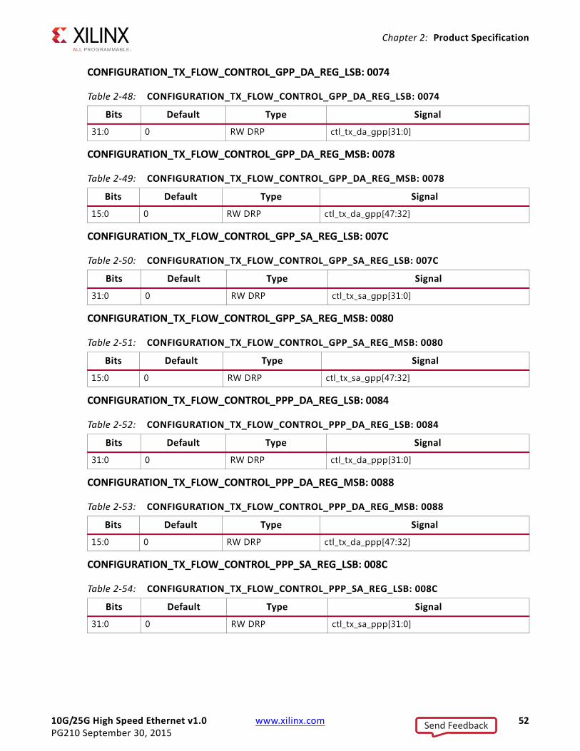
10G/25G High Speed Ethernet v1.0 www.xilinx.com 52PG210 September 30, 2015
Chapter 2: Product Specification
CONFIGURATION_TX_FLOW_CONTROL_GPP_DA_REG_LSB: 0074
CONFIGURATION_TX_FLOW_CONTROL_GPP_DA_REG_MSB: 0078
CONFIGURATION_TX_FLOW_CONTROL_GPP_SA_REG_LSB: 007C
CONFIGURATION_TX_FLOW_CONTROL_GPP_SA_REG_MSB: 0080
CONFIGURATION_TX_FLOW_CONTROL_PPP_DA_REG_LSB: 0084
CONFIGURATION_TX_FLOW_CONTROL_PPP_DA_REG_MSB: 0088
CONFIGURATION_TX_FLOW_CONTROL_PPP_SA_REG_LSB: 008C
Table 2‐48: CONFIGURATION_TX_FLOW_CONTROL_GPP_DA_REG_LSB: 0074
Bits Default Type Signal
31:0 0 RW DRP ctl_tx_da_gpp[31:0]
Table 2‐49: CONFIGURATION_TX_FLOW_CONTROL_GPP_DA_REG_MSB: 0078
Bits Default Type Signal
15:0 0 RW DRP ctl_tx_da_gpp[47:32]
Table 2‐50: CONFIGURATION_TX_FLOW_CONTROL_GPP_SA_REG_LSB: 007C
Bits Default Type Signal
31:0 0 RW DRP ctl_tx_sa_gpp[31:0]
Table 2‐51: CONFIGURATION_TX_FLOW_CONTROL_GPP_SA_REG_MSB: 0080
Bits Default Type Signal
15:0 0 RW DRP ctl_tx_sa_gpp[47:32]
Table 2‐52: CONFIGURATION_TX_FLOW_CONTROL_PPP_DA_REG_LSB: 0084
Bits Default Type Signal
31:0 0 RW DRP ctl_tx_da_ppp[31:0]
Table 2‐53: CONFIGURATION_TX_FLOW_CONTROL_PPP_DA_REG_MSB: 0088
Bits Default Type Signal
15:0 0 RW DRP ctl_tx_da_ppp[47:32]
Table 2‐54: CONFIGURATION_TX_FLOW_CONTROL_PPP_SA_REG_LSB: 008C
Bits Default Type Signal
31:0 0 RW DRP ctl_tx_sa_ppp[31:0]
Send Feedback
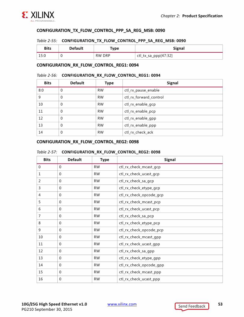
10G/25G High Speed Ethernet v1.0 www.xilinx.com 53PG210 September 30, 2015
Chapter 2: Product Specification
CONFIGURATION_TX_FLOW_CONTROL_PPP_SA_REG_MSB: 0090
CONFIGURATION_RX_FLOW_CONTROL_REG1: 0094
CONFIGURATION_RX_FLOW_CONTROL_REG2: 0098
Table 2‐55: CONFIGURATION_TX_FLOW_CONTROL_PPP_SA_REG_MSB: 0090
Bits Default Type Signal
15:0 0 RW DRP ctl_tx_sa_ppp[47:32]
Table 2‐56: CONFIGURATION_RX_FLOW_CONTROL_REG1: 0094
Bits Default Type Signal
8:0 0 RW ctl_rx_pause_enable
9 0 RW ctl_rx_forward_control
10 0 RW ctl_rx_enable_gcp
11 0 RW ctl_rx_enable_pcp
12 0 RW ctl_rx_enable_gpp
13 0 RW ctl_rx_enable_ppp
14 0 RW ctl_rx_check_ack
Table 2‐57: CONFIGURATION_RX_FLOW_CONTROL_REG2: 0098
Bits Default Type Signal
0 0 RW ctl_rx_check_mcast_gcp
1 0 RW ctl_rx_check_ucast_gcp
2 0 RW ctl_rx_check_sa_gcp
3 0 RW ctl_rx_check_etype_gcp
4 0 RW ctl_rx_check_opcode_gcp
5 0 RW ctl_rx_check_mcast_pcp
6 0 RW ctl_rx_check_ucast_pcp
7 0 RW ctl_rx_check_sa_pcp
8 0 RW ctl_rx_check_etype_pcp
9 0 RW ctl_rx_check_opcode_pcp
10 0 RW ctl_rx_check_mcast_gpp
11 0 RW ctl_rx_check_ucast_gpp
12 0 RW ctl_rx_check_sa_gpp
13 0 RW ctl_rx_check_etype_gpp
14 0 RW ctl_rx_check_opcode_gpp
15 0 RW ctl_rx_check_mcast_ppp
16 0 RW ctl_rx_check_ucast_ppp
Send Feedback

10G/25G High Speed Ethernet v1.0 www.xilinx.com 54PG210 September 30, 2015
Chapter 2: Product Specification
CONFIGURATION_RX_FLOW_CONTROL_PPP_ETYPE_OP_REG: 009C
CONFIGURATION_RX_FLOW_CONTROL_GPP_ETYPE_OP_REG: 00A0
CONFIGURATION_RX_FLOW_CONTROL_GCP_PCP_TYPE_REG: 00A4
CONFIGURATION_RX_FLOW_CONTROL_PCP_OP_REG: 00A8
CONFIGURATION_RX_FLOW_CONTROL_GCP_OP_REG: 00AC
17 0 RW ctl_rx_check_sa_ppp
18 0 RW ctl_rx_check_etype_ppp
19 0 RW ctl_rx_check_opcode_ppp
Table 2‐58: CONFIGURATION_RX_FLOW_CONTROL_PPP_ETYPE_OP_REG: 009C
Bits Default Type Signal
15:0 34824 RW DRP ctl_rx_etype_ppp
31:16 257 RW DRP ctl_rx_opcode_ppp
Table 2‐59: CONFIGURATION_RX_FLOW_CONTROL_GPP_ETYPE_OP_REG: 00A0
Bits Default Type Signal
15:0 34824 RW DRP ctl_rx_etype_gpp
31:16 1 RW DRP ctl_rx_opcode_gpp
Table 2‐60: CONFIGURATION_RX_FLOW_CONTROL_GCP_PCP_TYPE_REG: 00A4
Bits Default Type Signal
15:0 34824 RW DRP ctl_rx_etype_gcp
31:16 34824 RW DRP ctl_rx_etype_pcp
Table 2‐61: CONFIGURATION_RX_FLOW_CONTROL_PCP_OP_REG: 00A8
Bits Default Type Signal
15:0 257 RW DRP ctl_rx_opcode_min_pcp
31:16 257 RW DRP ctl_rx_opcode_max_pcp
Table 2‐62: CONFIGURATION_RX_FLOW_CONTROL_GCP_OP_REG: 00AC
Bits Default Type Signal
15:0 1 RW DRP ctl_rx_opcode_min_gcp
31:16 6 RW DRP ctl_rx_opcode_max_gcp
Table 2‐57: CONFIGURATION_RX_FLOW_CONTROL_REG2: 0098 (Cont’d)
Bits Default Type Signal
Send Feedback
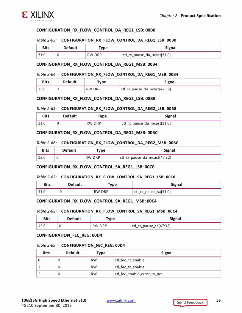
10G/25G High Speed Ethernet v1.0 www.xilinx.com 55PG210 September 30, 2015
Chapter 2: Product Specification
CONFIGURATION_RX_FLOW_CONTROL_DA_REG1_LSB: 00B0
CONFIGURATION_RX_FLOW_CONTROL_DA_REG1_MSB: 00B4
CONFIGURATION_RX_FLOW_CONTROL_DA_REG2_LSB: 00B8
CONFIGURATION_RX_FLOW_CONTROL_DA_REG2_MSB: 00BC
CONFIGURATION_RX_FLOW_CONTROL_SA_REG1_LSB: 00C0
CONFIGURATION_RX_FLOW_CONTROL_SA_REG1_MSB: 00C4
CONFIGURATION_FEC_REG: 00D4
Table 2‐63: CONFIGURATION_RX_FLOW_CONTROL_DA_REG1_LSB: 00B0
Bits Default Type Signal
31:0 0 RW DRP ctl_rx_pause_da_ucast[31:0]
Table 2‐64: CONFIGURATION_RX_FLOW_CONTROL_DA_REG1_MSB: 00B4
Bits Default Type Signal
15:0 0 RW DRP ctl_rx_pause_da_ucast[47:32]
Table 2‐65: CONFIGURATION_RX_FLOW_CONTROL_DA_REG2_LSB: 00B8
Bits Default Type Signal
31:0 0 RW DRP ctl_rx_pause_da_mcast[31:0]
Table 2‐66: CONFIGURATION_RX_FLOW_CONTROL_DA_REG2_MSB: 00BC
Bits Default Type Signal
15:0 0 RW DRP ctl_rx_pause_da_mcast[47:32]
Table 2‐67: CONFIGURATION_RX_FLOW_CONTROL_SA_REG1_LSB: 00C0
Bits Default Type Signal
31:0 0 RW DRP ctl_rx_pause_sa[31:0]
Table 2‐68: CONFIGURATION_RX_FLOW_CONTROL_SA_REG1_MSB: 00C4
Bits Default Type Signal
15:0 0 RW DRP ctl_rx_pause_sa[47:32]
Table 2‐69: CONFIGURATION_FEC_REG: 00D4
Bits Default Type Signal
0 0 RW ctl_fec_rx_enable
1 0 RW ctl_fec_tx_enable
2 0 RW ctl_fec_enable_error_to_pcs
Send Feedback
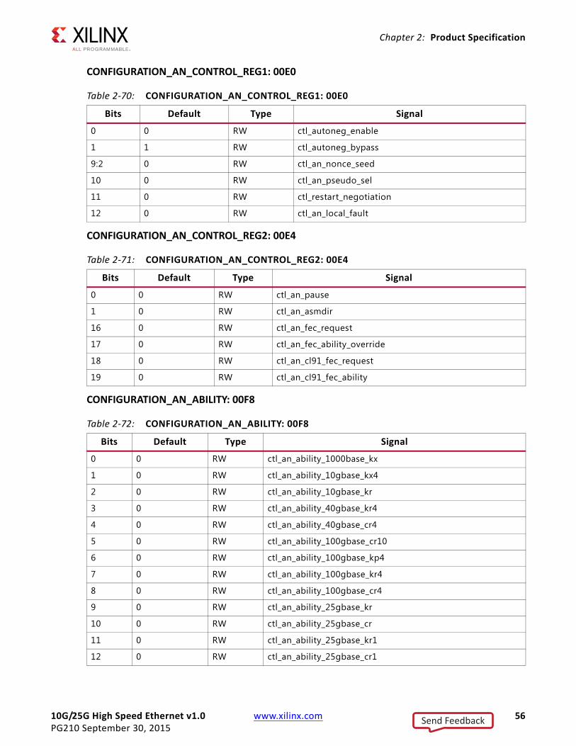
10G/25G High Speed Ethernet v1.0 www.xilinx.com 56PG210 September 30, 2015
Chapter 2: Product Specification
CONFIGURATION_AN_CONTROL_REG1: 00E0
CONFIGURATION_AN_CONTROL_REG2: 00E4
CONFIGURATION_AN_ABILITY: 00F8
Table 2‐70: CONFIGURATION_AN_CONTROL_REG1: 00E0
Bits Default Type Signal
0 0 RW ctl_autoneg_enable
1 1 RW ctl_autoneg_bypass
9:2 0 RW ctl_an_nonce_seed
10 0 RW ctl_an_pseudo_sel
11 0 RW ctl_restart_negotiation
12 0 RW ctl_an_local_fault
Table 2‐71: CONFIGURATION_AN_CONTROL_REG2: 00E4
Bits Default Type Signal
0 0 RW ctl_an_pause
1 0 RW ctl_an_asmdir
16 0 RW ctl_an_fec_request
17 0 RW ctl_an_fec_ability_override
18 0 RW ctl_an_cl91_fec_request
19 0 RW ctl_an_cl91_fec_ability
Table 2‐72: CONFIGURATION_AN_ABILITY: 00F8
Bits Default Type Signal
0 0 RW ctl_an_ability_1000base_kx
1 0 RW ctl_an_ability_10gbase_kx4
2 0 RW ctl_an_ability_10gbase_kr
3 0 RW ctl_an_ability_40gbase_kr4
4 0 RW ctl_an_ability_40gbase_cr4
5 0 RW ctl_an_ability_100gbase_cr10
6 0 RW ctl_an_ability_100gbase_kp4
7 0 RW ctl_an_ability_100gbase_kr4
8 0 RW ctl_an_ability_100gbase_cr4
9 0 RW ctl_an_ability_25gbase_kr
10 0 RW ctl_an_ability_25gbase_cr
11 0 RW ctl_an_ability_25gbase_kr1
12 0 RW ctl_an_ability_25gbase_cr1
Send Feedback
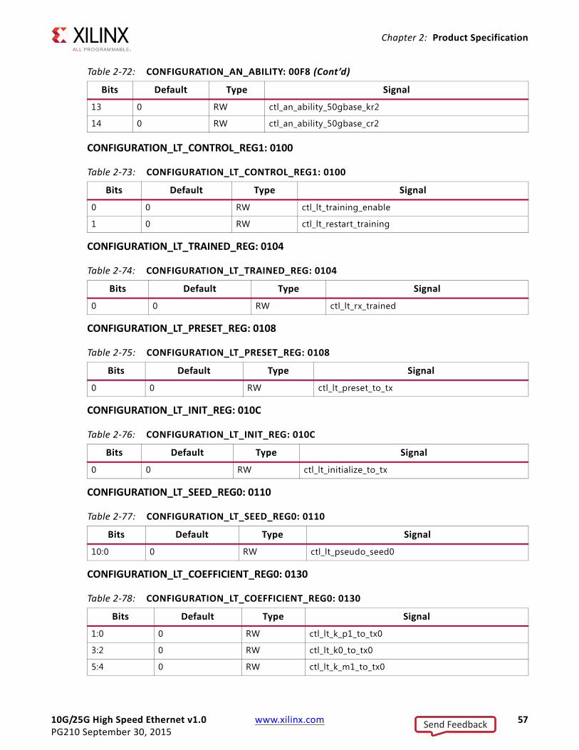
10G/25G High Speed Ethernet v1.0 www.xilinx.com 57PG210 September 30, 2015
Chapter 2: Product Specification
CONFIGURATION_LT_CONTROL_REG1: 0100
CONFIGURATION_LT_TRAINED_REG: 0104
CONFIGURATION_LT_PRESET_REG: 0108
CONFIGURATION_LT_INIT_REG: 010C
CONFIGURATION_LT_SEED_REG0: 0110
CONFIGURATION_LT_COEFFICIENT_REG0: 0130
13 0 RW ctl_an_ability_50gbase_kr2
14 0 RW ctl_an_ability_50gbase_cr2
Table 2‐73: CONFIGURATION_LT_CONTROL_REG1: 0100
Bits Default Type Signal
0 0 RW ctl_lt_training_enable
1 0 RW ctl_lt_restart_training
Table 2‐74: CONFIGURATION_LT_TRAINED_REG: 0104
Bits Default Type Signal
0 0 RW ctl_lt_rx_trained
Table 2‐75: CONFIGURATION_LT_PRESET_REG: 0108
Bits Default Type Signal
0 0 RW ctl_lt_preset_to_tx
Table 2‐76: CONFIGURATION_LT_INIT_REG: 010C
Bits Default Type Signal
0 0 RW ctl_lt_initialize_to_tx
Table 2‐77: CONFIGURATION_LT_SEED_REG0: 0110
Bits Default Type Signal
10:0 0 RW ctl_lt_pseudo_seed0
Table 2‐78: CONFIGURATION_LT_COEFFICIENT_REG0: 0130
Bits Default Type Signal
1:0 0 RW ctl_lt_k_p1_to_tx0
3:2 0 RW ctl_lt_k0_to_tx0
5:4 0 RW ctl_lt_k_m1_to_tx0
Table 2‐72: CONFIGURATION_AN_ABILITY: 00F8 (Cont’d)
Bits Default Type Signal
Send Feedback
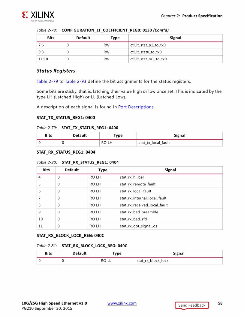
10G/25G High Speed Ethernet v1.0 www.xilinx.com 58PG210 September 30, 2015
Chapter 2: Product Specification
Status Registers
Table 2-79 to Table 2-93 define the bit assignments for the status registers.
Some bits are sticky, that is, latching their value high or low once set. This is indicated by the type LH (Latched High) or LL (Latched Low).
A description of each signal is found in Port Descriptions.
STAT_TX_STATUS_REG1: 0400
STAT_RX_STATUS_REG1: 0404
STAT_RX_BLOCK_LOCK_REG: 040C
7:6 0 RW ctl_lt_stat_p1_to_tx0
9:8 0 RW ctl_lt_stat0_to_tx0
11:10 0 RW ctl_lt_stat_m1_to_tx0
Table 2‐79: STAT_TX_STATUS_REG1: 0400
Bits Default Type Signal
0 0 RO LH stat_tx_local_fault
Table 2‐80: STAT_RX_STATUS_REG1: 0404
Bits Default Type Signal
4 0 RO LH stat_rx_hi_ber
5 0 RO LH stat_rx_remote_fault
6 0 RO LH stat_rx_local_fault
7 0 RO LH stat_rx_internal_local_fault
8 0 RO LH stat_rx_received_local_fault
9 0 RO LH stat_rx_bad_preamble
10 0 RO LH stat_rx_bad_sfd
11 0 RO LH stat_rx_got_signal_os
Table 2‐81: STAT_RX_BLOCK_LOCK_REG: 040C
Bits Default Type Signal
0 0 RO LL stat_rx_block_lock
Table 2‐78: CONFIGURATION_LT_COEFFICIENT_REG0: 0130 (Cont’d)
Bits Default Type Signal
Send Feedback
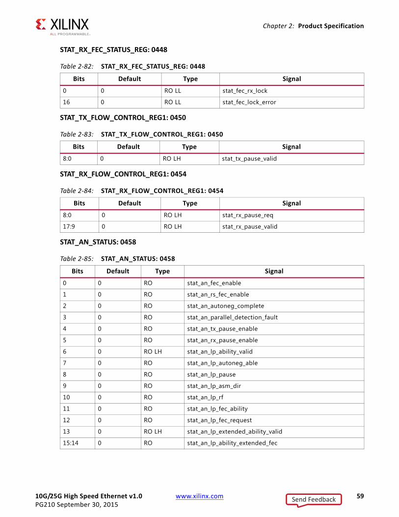
10G/25G High Speed Ethernet v1.0 www.xilinx.com 59PG210 September 30, 2015
Chapter 2: Product Specification
STAT_RX_FEC_STATUS_REG: 0448
STAT_TX_FLOW_CONTROL_REG1: 0450
STAT_RX_FLOW_CONTROL_REG1: 0454
STAT_AN_STATUS: 0458
Table 2‐82: STAT_RX_FEC_STATUS_REG: 0448
Bits Default Type Signal
0 0 RO LL stat_fec_rx_lock
16 0 RO LL stat_fec_lock_error
Table 2‐83: STAT_TX_FLOW_CONTROL_REG1: 0450
Bits Default Type Signal
8:0 0 RO LH stat_tx_pause_valid
Table 2‐84: STAT_RX_FLOW_CONTROL_REG1: 0454
Bits Default Type Signal
8:0 0 RO LH stat_rx_pause_req
17:9 0 RO LH stat_rx_pause_valid
Table 2‐85: STAT_AN_STATUS: 0458
Bits Default Type Signal
0 0 RO stat_an_fec_enable
1 0 RO stat_an_rs_fec_enable
2 0 RO stat_an_autoneg_complete
3 0 RO stat_an_parallel_detection_fault
4 0 RO stat_an_tx_pause_enable
5 0 RO stat_an_rx_pause_enable
6 0 RO LH stat_an_lp_ability_valid
7 0 RO stat_an_lp_autoneg_able
8 0 RO stat_an_lp_pause
9 0 RO stat_an_lp_asm_dir
10 0 RO stat_an_lp_rf
11 0 RO stat_an_lp_fec_ability
12 0 RO stat_an_lp_fec_request
13 0 RO LH stat_an_lp_extended_ability_valid
15:14 0 RO stat_an_lp_ability_extended_fec
Send Feedback
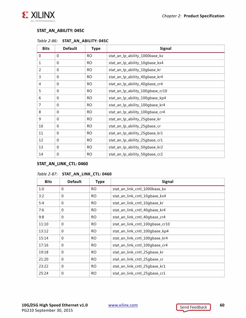
10G/25G High Speed Ethernet v1.0 www.xilinx.com 60PG210 September 30, 2015
Chapter 2: Product Specification
STAT_AN_ABILITY: 045C
STAT_AN_LINK_CTL: 0460
Table 2‐86: STAT_AN_ABILITY: 045C
Bits Default Type Signal
0 0 RO stat_an_lp_ability_1000base_kx
1 0 RO stat_an_lp_ability_10gbase_kx4
2 0 RO stat_an_lp_ability_10gbase_kr
3 0 RO stat_an_lp_ability_40gbase_kr4
4 0 RO stat_an_lp_ability_40gbase_cr4
5 0 RO stat_an_lp_ability_100gbase_cr10
6 0 RO stat_an_lp_ability_100gbase_kp4
7 0 RO stat_an_lp_ability_100gbase_kr4
8 0 RO stat_an_lp_ability_100gbase_cr4
9 0 RO stat_an_lp_ability_25gbase_kr
10 0 RO stat_an_lp_ability_25gbase_cr
11 0 RO stat_an_lp_ability_25gbase_kr1
12 0 RO stat_an_lp_ability_25gbase_cr1
13 0 RO stat_an_lp_ability_50gbase_kr2
14 0 RO stat_an_lp_ability_50gbase_cr2
Table 2‐87: STAT_AN_LINK_CTL: 0460
Bits Default Type Signal
1:0 0 RO stat_an_link_cntl_1000base_kx
3:2 0 RO stat_an_link_cntl_10gbase_kx4
5:4 0 RO stat_an_link_cntl_10gbase_kr
7:6 0 RO stat_an_link_cntl_40gbase_kr4
9:8 0 RO stat_an_link_cntl_40gbase_cr4
11:10 0 RO stat_an_link_cntl_100gbase_cr10
13:12 0 RO stat_an_link_cntl_100gbase_kp4
15:14 0 RO stat_an_link_cntl_100gbase_kr4
17:16 0 RO stat_an_link_cntl_100gbase_cr4
19:18 0 RO stat_an_link_cntl_25gbase_kr
21:20 0 RO stat_an_link_cntl_25gbase_cr
23:22 0 RO stat_an_link_cntl_25gbase_kr1
25:24 0 RO stat_an_link_cntl_25gbase_cr1
Send Feedback
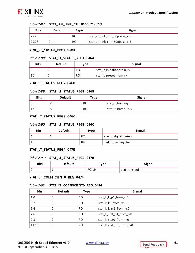
10G/25G High Speed Ethernet v1.0 www.xilinx.com 61PG210 September 30, 2015
Chapter 2: Product Specification
STAT_LT_STATUS_REG1: 0464
STAT_LT_STATUS_REG2: 0468
STAT_LT_STATUS_REG3: 046C
STAT_LT_STATUS_REG4: 0470
STAT_LT_COEFFICIENT0_REG: 0474
27:26 0 RO stat_an_link_cntl_50gbase_kr2
29:28 0 RO stat_an_link_cntl_50gbase_cr2
Table 2‐88: STAT_LT_STATUS_REG1: 0464
Bits Default Type Signal
0 0 RO stat_lt_initialize_from_rx
16 0 RO stat_lt_preset_from_rx
Table 2‐89: STAT_LT_STATUS_REG2: 0468
Bits Default Type Signal
0 0 RO stat_lt_training
16 0 RO stat_lt_frame_lock
Table 2‐90: STAT_LT_STATUS_REG3: 046C
Bits Default Type Signal
0 0 RO stat_lt_signal_detect
16 0 RO stat_lt_training_fail
Table 2‐91: STAT_LT_STATUS_REG4: 0470
Bits Default Type Signal
0 0 RO LH stat_lt_rx_sof
Table 2‐92: STAT_LT_COEFFICIENT0_REG: 0474
Bits Default Type Signal
1:0 0 RO stat_lt_k_p1_from_rx0
3:2 0 RO stat_lt_k0_from_rx0
5:4 0 RO stat_lt_k_m1_from_rx0
7:6 0 RO stat_lt_stat_p1_from_rx0
9:8 0 RO stat_lt_stat0_from_rx0
11:10 0 RO stat_lt_stat_m1_from_rx0
Table 2‐87: STAT_AN_LINK_CTL: 0460 (Cont’d)
Bits Default Type Signal
Send Feedback
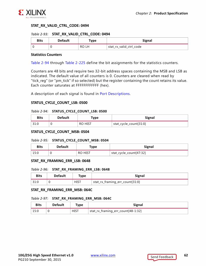
10G/25G High Speed Ethernet v1.0 www.xilinx.com 62PG210 September 30, 2015
Chapter 2: Product Specification
STAT_RX_VALID_CTRL_CODE: 0494
Statistics Counters
Table 2-94 through Table 2-225 define the bit assignments for the statistics counters.
Counters are 48 bits and require two 32-bit address spaces containing the MSB and LSB as indicated. The default value of all counters is 0. Counters are cleared when read by "tick_reg" (or "pm_tick" if so selected) but the register containing the count retains its value. Each counter saturates at FFFFFFFFFFFF (hex).
A description of each signal is found in Port Descriptions.
STATUS_CYCLE_COUNT_LSB: 0500
STATUS_CYCLE_COUNT_MSB: 0504
STAT_RX_FRAMING_ERR_LSB: 0648
STAT_RX_FRAMING_ERR_MSB: 064C
Table 2‐93: STAT_RX_VALID_CTRL_CODE: 0494
Bits Default Type Signal
0 0 RO LH stat_rx_valid_ctrl_code
Table 2‐94: STATUS_CYCLE_COUNT_LSB: 0500
Bits Default Type Signal
31:0 0 RO HIST stat_cycle_count[31:0]
Table 2‐95: STATUS_CYCLE_COUNT_MSB: 0504
Bits Default Type Signal
15:0 0 RO HIST stat_cycle_count[47:32]
Table 2‐96: STAT_RX_FRAMING_ERR_LSB: 0648
Bits Default Type Signal
31:0 0 HIST stat_rx_framing_err_count[31:0]
Table 2‐97: STAT_RX_FRAMING_ERR_MSB: 064C
Bits Default Type Signal
15:0 0 HIST stat_rx_framing_err_count[48-1:32]
Send Feedback
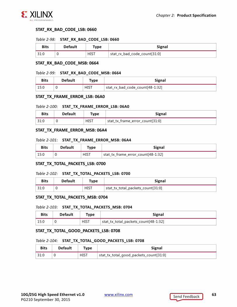
10G/25G High Speed Ethernet v1.0 www.xilinx.com 63PG210 September 30, 2015
Chapter 2: Product Specification
STAT_RX_BAD_CODE_LSB: 0660
STAT_RX_BAD_CODE_MSB: 0664
STAT_TX_FRAME_ERROR_LSB: 06A0
STAT_TX_FRAME_ERROR_MSB: 06A4
STAT_TX_TOTAL_PACKETS_LSB: 0700
STAT_TX_TOTAL_PACKETS_MSB: 0704
STAT_TX_TOTAL_GOOD_PACKETS_LSB: 0708
Table 2‐98: STAT_RX_BAD_CODE_LSB: 0660
Bits Default Type Signal
31:0 0 HIST stat_rx_bad_code_count[31:0]
Table 2‐99: STAT_RX_BAD_CODE_MSB: 0664
Bits Default Type Signal
15:0 0 HIST stat_rx_bad_code_count[48-1:32]
Table 2‐100: STAT_TX_FRAME_ERROR_LSB: 06A0
Bits Default Type Signal
31:0 0 HIST stat_tx_frame_error_count[31:0]
Table 2‐101: STAT_TX_FRAME_ERROR_MSB: 06A4
Bits Default Type Signal
15:0 0 HIST stat_tx_frame_error_count[48-1:32]
Table 2‐102: STAT_TX_TOTAL_PACKETS_LSB: 0700
Bits Default Type Signal
31:0 0 HIST stat_tx_total_packets_count[31:0]
Table 2‐103: STAT_TX_TOTAL_PACKETS_MSB: 0704
Bits Default Type Signal
15:0 0 HIST stat_tx_total_packets_count[48-1:32]
Table 2‐104: STAT_TX_TOTAL_GOOD_PACKETS_LSB: 0708
Bits Default Type Signal
31:0 0 HIST stat_tx_total_good_packets_count[31:0]
Send Feedback
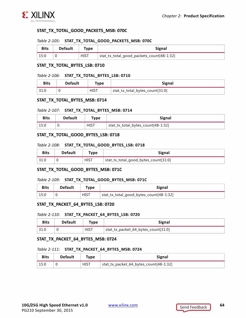
10G/25G High Speed Ethernet v1.0 www.xilinx.com 64PG210 September 30, 2015
Chapter 2: Product Specification
STAT_TX_TOTAL_GOOD_PACKETS_MSB: 070C
STAT_TX_TOTAL_BYTES_LSB: 0710
STAT_TX_TOTAL_BYTES_MSB: 0714
STAT_TX_TOTAL_GOOD_BYTES_LSB: 0718
STAT_TX_TOTAL_GOOD_BYTES_MSB: 071C
STAT_TX_PACKET_64_BYTES_LSB: 0720
STAT_TX_PACKET_64_BYTES_MSB: 0724
Table 2‐105: STAT_TX_TOTAL_GOOD_PACKETS_MSB: 070C
Bits Default Type Signal
15:0 0 HIST stat_tx_total_good_packets_count[48-1:32]
Table 2‐106: STAT_TX_TOTAL_BYTES_LSB: 0710
Bits Default Type Signal
31:0 0 HIST stat_tx_total_bytes_count[31:0]
Table 2‐107: STAT_TX_TOTAL_BYTES_MSB: 0714
Bits Default Type Signal
15:0 0 HIST stat_tx_total_bytes_count[48-1:32]
Table 2‐108: STAT_TX_TOTAL_GOOD_BYTES_LSB: 0718
Bits Default Type Signal
31:0 0 HIST stat_tx_total_good_bytes_count[31:0]
Table 2‐109: STAT_TX_TOTAL_GOOD_BYTES_MSB: 071C
Bits Default Type Signal
15:0 0 HIST stat_tx_total_good_bytes_count[48-1:32]
Table 2‐110: STAT_TX_PACKET_64_BYTES_LSB: 0720
Bits Default Type Signal
31:0 0 HIST stat_tx_packet_64_bytes_count[31:0]
Table 2‐111: STAT_TX_PACKET_64_BYTES_MSB: 0724
Bits Default Type Signal
15:0 0 HIST stat_tx_packet_64_bytes_count[48-1:32]
Send Feedback

10G/25G High Speed Ethernet v1.0 www.xilinx.com 65PG210 September 30, 2015
Chapter 2: Product Specification
STAT_TX_PACKET_65_127_BYTES_LSB: 0728
STAT_TX_PACKET_65_127_BYTES_MSB: 072C
STAT_TX_PACKET_128_255_BYTES_LSB: 0730
STAT_TX_PACKET_128_255_BYTES_MSB: 0734
STAT_TX_PACKET_256_511_BYTES_LSB: 0738
STAT_TX_PACKET_256_511_BYTES_MSB: 073C
STAT_TX_PACKET_512_1023_BYTES_LSB: 0740
Table 2‐112: STAT_TX_PACKET_65_127_BYTES_LSB: 0728
Bits Default Type Signal
31:0 0 HIST stat_tx_packet_65_127_bytes_count[31:0]
Table 2‐113: STAT_TX_PACKET_65_127_BYTES_MSB: 072C
Bits Default Type Signal
15:0 0 HIST stat_tx_packet_65_127_bytes_count[48-1:32]
Table 2‐114: STAT_TX_PACKET_128_255_BYTES_LSB: 0730
Bits Default Type Signal
31:0 0 HIST stat_tx_packet_128_255_bytes_count[31:0]
Table 2‐115: STAT_TX_PACKET_128_255_BYTES_MSB: 0734
Bits Default Type Signal
15:0 0 HIST stat_tx_packet_128_255_bytes_count[48-1:32]
Table 2‐116: STAT_TX_PACKET_256_511_BYTES_LSB: 0738
Bits Default Type Signal
31:0 0 HIST stat_tx_packet_256_511_bytes_count[31:0]
Table 2‐117: STAT_TX_PACKET_256_511_BYTES_MSB: 073C
Bits Default Type Signal
15:0 0 HIST stat_tx_packet_256_511_bytes_count[48-1:32]
Table 2‐118: STAT_TX_PACKET_512_1023_BYTES_LSB: 0740
Bits Default Type Signal
31:0 0 HIST stat_tx_packet_512_1023_bytes_count[31:0]
Send Feedback

10G/25G High Speed Ethernet v1.0 www.xilinx.com 66PG210 September 30, 2015
Chapter 2: Product Specification
STAT_TX_PACKET_512_1023_BYTES_MSB: 0744
STAT_TX_PACKET_1024_1518_BYTES_LSB: 0748
STAT_TX_PACKET_1024_1518_BYTES_MSB: 074C
STAT_TX_PACKET_1519_1522_BYTES_LSB: 0750
STAT_TX_PACKET_1519_1522_BYTES_MSB: 0754
STAT_TX_PACKET_1523_1548_BYTES_LSB: 0758
STAT_TX_PACKET_1523_1548_BYTES_MSB: 075C
Table 2‐119: STAT_TX_PACKET_512_1023_BYTES_MSB: 0744
Bits Default Type Signal
15:0 0 HIST stat_tx_packet_512_1023_bytes_count[48-1:32]
Table 2‐120: STAT_TX_PACKET_1024_1518_BYTES_LSB: 0748
Bits Default Type Signal
31:0 0 HIST stat_tx_packet_1024_1518_bytes_count[31:0]
Table 2‐121: STAT_TX_PACKET_1024_1518_BYTES_MSB: 074C
Bits Default Type Signal
15:0 0 HIST stat_tx_packet_1024_1518_bytes_count[48-1:32]
Table 2‐122: STAT_TX_PACKET_1519_1522_BYTES_LSB: 0750
Bits Default Type Signal
31:0 0 HIST stat_tx_packet_1519_1522_bytes_count[31:0]
Table 2‐123: STAT_TX_PACKET_1519_1522_BYTES_MSB: 0754
Bits Default Type Signal
15:0 0 HIST stat_tx_packet_1519_1522_bytes_count[48-1:32]
Table 2‐124: STAT_TX_PACKET_1523_1548_BYTES_LSB: 0758
Bits Default Type Signal
31:0 0 HIST stat_tx_packet_1523_1548_bytes_count[31:0]
Table 2‐125: STAT_TX_PACKET_1523_1548_BYTES_MSB: 075C
Bits Default Type Signal
15:0 0 HIST stat_tx_packet_1523_1548_bytes_count[48-1:32]
Send Feedback
10G/25G High Speed Ethernet v1.0 www.xilinx.com 67PG210 September 30, 2015
Chapter 2: Product Specification
STAT_TX_PACKET_1549_2047_BYTES_LSB: 0760
STAT_TX_PACKET_1549_2047_BYTES_MSB: 0764
STAT_TX_PACKET_2048_4095_BYTES_LSB: 0768
STAT_TX_PACKET_2048_4095_BYTES_MSB: 076C
STAT_TX_PACKET_4096_8191_BYTES_LSB: 0770
STAT_TX_PACKET_4096_8191_BYTES_MSB: 0774
STAT_TX_PACKET_8192_9215_BYTES_LSB: 0778
Table 2‐126: STAT_TX_PACKET_1549_2047_BYTES_LSB: 0760
Bits Default Type Signal
31:0 0 HIST stat_tx_packet_1549_2047_bytes_count[31:0]
Table 2‐127: STAT_TX_PACKET_1549_2047_BYTES_MSB: 0764
Bits Default Type Signal
15:0 0 HIST stat_tx_packet_1549_2047_bytes_count[48-1:32]
Table 2‐128: STAT_TX_PACKET_2048_4095_BYTES_LSB: 0768
Bits Default Type Signal
31:0 0 HIST stat_tx_packet_2048_4095_bytes_count[31:0]
Table 2‐129: STAT_TX_PACKET_2048_4095_BYTES_MSB: 076C
Bits Default Type Signal
15:0 0 HIST stat_tx_packet_2048_4095_bytes_count[48-1:32]
Table 2‐130: STAT_TX_PACKET_4096_8191_BYTES_LSB: 0770
Bits Default Type Signal
31:0 0 HIST stat_tx_packet_4096_8191_bytes_count[31:0]
Table 2‐131: STAT_TX_PACKET_4096_8191_BYTES_MSB: 0774
Bits Default Type Signal
15:0 0 HIST stat_tx_packet_4096_8191_bytes_count[48-1:32]
Table 2‐132: STAT_TX_PACKET_8192_9215_BYTES_LSB: 0778
Bits Default Type Signal
31:0 0 HIST stat_tx_packet_8192_9215_bytes_count[31:0]
Send Feedback
10G/25G High Speed Ethernet v1.0 www.xilinx.com 68PG210 September 30, 2015
Chapter 2: Product Specification
STAT_TX_PACKET_8192_9215_BYTES_MSB: 077C
STAT_TX_PACKET_LARGE_LSB: 0780
STAT_TX_PACKET_LARGE_MSB: 0784
STAT_TX_PACKET_SMALL_LSB: 0788
STAT_TX_PACKET_SMALL_MSB: 078C
STAT_TX_BAD_FCS_LSB: 07B8
STAT_TX_BAD_FCS_MSB: 07BC
Table 2‐133: STAT_TX_PACKET_8192_9215_BYTES_MSB: 077C
Bits Default Type Signal
15:0 0 HIST stat_tx_packet_8192_9215_bytes_count[48-1:32]
Table 2‐134: STAT_TX_PACKET_LARGE_LSB: 0780
Bits Default Type Signal
31:0 0 HIST stat_tx_packet_large_count[31:0]
Table 2‐135: STAT_TX_PACKET_LARGE_MSB: 0784
Bits Default Type Signal
15:0 0 HIST stat_tx_packet_large_count[48-1:32]
Table 2‐136: STAT_TX_PACKET_SMALL_LSB: 0788
Bits Default Type Signal
31:0 0 HIST stat_tx_packet_small_count[31:0]
Table 2‐137: STAT_TX_PACKET_SMALL_MSB: 078C
Bits Default Type Signal
15:0 0 HIST stat_tx_packet_small_count[48-1:32]
Table 2‐138: STAT_TX_BAD_FCS_LSB: 07B8
Bits Default Type Signal
31:0 0 HIST stat_tx_bad_fcs_count[31:0]
Table 2‐139: STAT_TX_BAD_FCS_MSB: 07BC
Bits Default Type Signal
15:0 0 HIST stat_tx_bad_fcs_count[48-1:32]
Send Feedback
10G/25G High Speed Ethernet v1.0 www.xilinx.com 69PG210 September 30, 2015
Chapter 2: Product Specification
STAT_TX_UNICAST_LSB: 07D0
STAT_TX_UNICAST_MSB: 07D4
STAT_TX_MULTICAST_LSB: 07D8
STAT_TX_MULTICAST_MSB: 07DC
STAT_TX_BROADCAST_LSB: 07E0
STAT_TX_BROADCAST_MSB: 07E4
STAT_TX_VLAN_LSB: 07E8
Table 2‐140: STAT_TX_UNICAST_LSB: 07D0
Bits Default Type Signal
31:0 0 HIST stat_tx_unicast_count[31:0]
Table 2‐141: STAT_TX_UNICAST_MSB: 07D4
Bits Default Type Signal
15:0 0 HIST stat_tx_unicast_count[48-1:32]
Table 2‐142: STAT_TX_MULTICAST_LSB: 07D8
Bits Default Type Signal
31:0 0 HIST stat_tx_multicast_count[31:0]
Table 2‐143: STAT_TX_MULTICAST_MSB: 07DC
Bits Default Type Signal
15:0 0 HIST stat_tx_multicast_count[48-1:32]
Table 2‐144: STAT_TX_BROADCAST_LSB: 07E0
Bits Default Type Signal
31:0 0 HIST stat_tx_broadcast_count[31:0]
Table 2‐145: STAT_TX_BROADCAST_MSB: 07E4
Bits Default Type Signal
15:0 0 HIST stat_tx_broadcast_count[48-1:32]
Table 2‐146: STAT_TX_VLAN_LSB: 07E8
Bits Default Type Signal
31:0 0 HIST stat_tx_vlan_count[31:0]
Send Feedback

10G/25G High Speed Ethernet v1.0 www.xilinx.com 70PG210 September 30, 2015
Chapter 2: Product Specification
STAT_TX_VLAN_MSB: 07EC
STAT_TX_PAUSE_LSB: 07F0
STAT_TX_PAUSE_MSB: 07F4
STAT_TX_USER_PAUSE_LSB: 07F8
STAT_TX_USER_PAUSE_MSB: 07FC
STAT_RX_TOTAL_PACKETS_LSB: 0808
STAT_RX_TOTAL_PACKETS_MSB: 080C
Table 2‐147: STAT_TX_VLAN_MSB: 07EC
Bits Default Type Signal
15:0 0 HIST stat_tx_vlan_count[48-1:32]
Table 2‐148: STAT_TX_PAUSE_LSB: 07F0
Bits Default Type Signal
31:0 0 HIST stat_tx_pause_count[31:0]
Table 2‐149: STAT_TX_PAUSE_MSB: 07F4
Bits Default Type Signal
15:0 0 HIST stat_tx_pause_count[48-1:32]
Table 2‐150: STAT_TX_USER_PAUSE_LSB: 07F8
Bits Default Type Signal
31:0 0 HIST stat_tx_user_pause_count[31:0]
Table 2‐151: STAT_TX_USER_PAUSE_MSB: 07FC
Bits Default Type Signal
15:0 0 HIST stat_tx_user_pause_count[48-1:32]
Table 2‐152: STAT_RX_TOTAL_PACKETS_LSB: 0808
Bits Default Type Signal
31:0 0 HIST stat_rx_total_packets_count[31:0]
Table 2‐153: STAT_RX_TOTAL_PACKETS_MSB: 080C
Bits Default Type Signal
15:0 0 HIST stat_rx_total_packets_count[48-1:32]
Send Feedback

10G/25G High Speed Ethernet v1.0 www.xilinx.com 71PG210 September 30, 2015
Chapter 2: Product Specification
STAT_RX_TOTAL_GOOD_PACKETS_LSB: 0810
STAT_RX_TOTAL_GOOD_PACKETS_MSB: 0814
STAT_RX_TOTAL_BYTES_LSB: 0818
STAT_RX_TOTAL_BYTES_MSB: 081C
STAT_RX_TOTAL_GOOD_BYTES_LSB: 0820
STAT_RX_TOTAL_GOOD_BYTES_MSB: 0824
STAT_RX_PACKET_64_BYTES_LSB: 0828
Table 2‐154: STAT_RX_TOTAL_GOOD_PACKETS_LSB: 0810
Bits Default Type Signal
31:0 0 HIST stat_rx_total_good_packets_count[31:0]
Table 2‐155: STAT_RX_TOTAL_GOOD_PACKETS_MSB: 0814
Bits Default Type Signal
15:0 0 HIST stat_rx_total_good_packets_count[48-1:32]
Table 2‐156: STAT_RX_TOTAL_BYTES_LSB: 0818
Bits Default Type Signal
31:0 0 HIST stat_rx_total_bytes_count[31:0]
Table 2‐157: STAT_RX_TOTAL_BYTES_MSB: 081C
Bits Default Type Signal
15:0 0 HIST stat_rx_total_bytes_count[48-1:32]
Table 2‐158: STAT_RX_TOTAL_GOOD_BYTES_LSB: 0820
Bits Default Type Signal
31:0 0 HIST stat_rx_total_good_bytes_count[31:0]
Table 2‐159: STAT_RX_TOTAL_GOOD_BYTES_MSB: 0824
Bits Default Type Signal
15:0 0 HIST stat_rx_total_good_bytes_count[48-1:32]
Table 2‐160: STAT_RX_PACKET_64_BYTES_LSB: 0828
Bits Default Type Signal
31:0 0 HIST stat_rx_packet_64_bytes_count[31:0]
Send Feedback

10G/25G High Speed Ethernet v1.0 www.xilinx.com 72PG210 September 30, 2015
Chapter 2: Product Specification
STAT_RX_PACKET_64_BYTES_MSB: 082C
STAT_RX_PACKET_65_127_BYTES_LSB: 0830
STAT_RX_PACKET_65_127_BYTES_MSB: 0834
STAT_RX_PACKET_128_255_BYTES_LSB: 0838
STAT_RX_PACKET_128_255_BYTES_MSB: 083C
STAT_RX_PACKET_256_511_BYTES_LSB: 0840
STAT_RX_PACKET_256_511_BYTES_MSB: 0844
Table 2‐161: STAT_RX_PACKET_64_BYTES_MSB: 082C
Bits Default Type Signal
15:0 0 HIST stat_rx_packet_64_bytes_count[48-1:32]
Table 2‐162: STAT_RX_PACKET_65_127_BYTES_LSB: 0830
Bits Default Type Signal
31:0 0 HIST stat_rx_packet_65_127_bytes_count[31:0]
Table 2‐163: STAT_RX_PACKET_65_127_BYTES_MSB: 0834
Bits Default Type Signal
15:0 0 HIST stat_rx_packet_65_127_bytes_count[48-1:32]
Table 2‐164: STAT_RX_PACKET_128_255_BYTES_LSB: 0838
Bits Default Type Signal
31:0 0 HIST stat_rx_packet_128_255_bytes_count[31:0]
Table 2‐165: STAT_RX_PACKET_128_255_BYTES_MSB: 083C
Bits Default Type Signal
15:0 0 HIST stat_rx_packet_128_255_bytes_count[48-1:32]
Table 2‐166: STAT_RX_PACKET_256_511_BYTES_LSB: 0840
Bits Default Type Signal
31:0 0 HIST stat_rx_packet_256_511_bytes_count[31:0]
Table 2‐167: STAT_RX_PACKET_256_511_BYTES_MSB: 0844
Bits Default Type Signal
15:0 0 HIST stat_rx_packet_256_511_bytes_count[48-1:32]
Send Feedback
10G/25G High Speed Ethernet v1.0 www.xilinx.com 73PG210 September 30, 2015
Chapter 2: Product Specification
STAT_RX_PACKET_512_1023_BYTES_LSB: 0848
STAT_RX_PACKET_512_1023_BYTES_MSB: 084C
STAT_RX_PACKET_1024_1518_BYTES_LSB: 0850
STAT_RX_PACKET_1024_1518_BYTES_MSB: 0854
STAT_RX_PACKET_1519_1522_BYTES_LSB: 0858
STAT_RX_PACKET_1519_1522_BYTES_MSB: 085C
STAT_RX_PACKET_1523_1548_BYTES_LSB: 0860
Table 2‐168: STAT_RX_PACKET_512_1023_BYTES_LSB: 0848
Bits Default Type Signal
31:0 0 HIST stat_rx_packet_512_1023_bytes_count[31:0]
Table 2‐169: STAT_RX_PACKET_512_1023_BYTES_MSB: 084C
Bits Default Type Signal
15:0 0 HIST stat_rx_packet_512_1023_bytes_count[48-1:32]
Table 2‐170: STAT_RX_PACKET_1024_1518_BYTES_LSB: 0850
Bits Default Type Signal
31:0 0 HIST stat_rx_packet_1024_1518_bytes_count[31:0]
Table 2‐171: STAT_RX_PACKET_1024_1518_BYTES_MSB: 0854
Bits Default Type Signal
15:0 0 HIST stat_rx_packet_1024_1518_bytes_count[48-1:32]
Table 2‐172: STAT_RX_PACKET_1519_1522_BYTES_LSB: 0858
Bits Default Type Signal
31:0 0 HIST stat_rx_packet_1519_1522_bytes_count[31:0]
Table 2‐173: STAT_RX_PACKET_1519_1522_BYTES_MSB: 085C
Bits Default Type Signal
15:0 0 HIST stat_rx_packet_1519_1522_bytes_count[48-1:32]
Table 2‐174: STAT_RX_PACKET_1523_1548_BYTES_LSB: 0860
Bits Default Type Signal
31:0 0 HIST stat_rx_packet_1523_1548_bytes_count[31:0]
Send Feedback

10G/25G High Speed Ethernet v1.0 www.xilinx.com 74PG210 September 30, 2015
Chapter 2: Product Specification
STAT_RX_PACKET_1523_1548_BYTES_MSB: 0864
STAT_RX_PACKET_1549_2047_BYTES_LSB: 0868
STAT_RX_PACKET_1549_2047_BYTES_MSB: 086C
STAT_RX_PACKET_2048_4095_BYTES_LSB: 0870
STAT_RX_PACKET_2048_4095_BYTES_MSB: 0874
STAT_RX_PACKET_4096_8191_BYTES_LSB: 0878
STAT_RX_PACKET_4096_8191_BYTES_MSB: 087C
Table 2‐175: STAT_RX_PACKET_1523_1548_BYTES_MSB: 0864
Bits Default Type Signal
15:0 0 HIST stat_rx_packet_1523_1548_bytes_count[48-1:32]
Table 2‐176: STAT_RX_PACKET_1549_2047_BYTES_LSB: 0868
Bits Default Type Signal
31:0 0 HIST stat_rx_packet_1549_2047_bytes_count[31:0]
Table 2‐177: STAT_RX_PACKET_1549_2047_BYTES_MSB: 086C
Bits Default Type Signal
15:0 0 HIST stat_rx_packet_1549_2047_bytes_count[48-1:32]
Table 2‐178: STAT_RX_PACKET_2048_4095_BYTES_LSB: 0870
Bits Default Type Signal
31:0 0 HIST stat_rx_packet_2048_4095_bytes_count[31:0]
Table 2‐179: STAT_RX_PACKET_2048_4095_BYTES_MSB: 0874
Bits Default Type Signal
15:0 0 HIST stat_rx_packet_2048_4095_bytes_count[48-1:32]
Table 2‐180: STAT_RX_PACKET_4096_8191_BYTES_LSB: 0878
Bits Default Type Signal
31:0 0 HIST stat_rx_packet_4096_8191_bytes_count[31:0]
Table 2‐181: STAT_RX_PACKET_4096_8191_BYTES_MSB: 087C
Bits Default Type Signal
15:0 0 HIST stat_rx_packet_4096_8191_bytes_count[48-1:32]
Send Feedback
10G/25G High Speed Ethernet v1.0 www.xilinx.com 75PG210 September 30, 2015
Chapter 2: Product Specification
STAT_RX_PACKET_8192_9215_BYTES_LSB: 0880
STAT_RX_PACKET_8192_9215_BYTES_MSB: 0884
STAT_RX_PACKET_LARGE_LSB: 0888
STAT_RX_PACKET_LARGE_MSB: 088C
STAT_RX_PACKET_SMALL_LSB: 0890
STAT_RX_PACKET_SMALL_MSB: 0894
STAT_RX_UNDERSIZE_LSB: 0898
Table 2‐182: STAT_RX_PACKET_8192_9215_BYTES_LSB: 0880
Bits Default Type Signal
31:0 0 HIST stat_rx_packet_8192_9215_bytes_count[31:0]
Table 2‐183: STAT_RX_PACKET_8192_9215_BYTES_MSB: 0884
Bits Default Type Signal
15:0 0 HIST stat_rx_packet_8192_9215_bytes_count[48-1:32]
Table 2‐184: STAT_RX_PACKET_LARGE_LSB: 0888
Bits Default Type Signal
31:0 0 HIST stat_rx_packet_large_count[31:0]
Table 2‐185: STAT_RX_PACKET_LARGE_MSB: 088C
Bits Default Type Signal
15:0 0 HIST stat_rx_packet_large_count[48-1:32]
Table 2‐186: STAT_RX_PACKET_SMALL_LSB: 0890
Bits Default Type Signal
31:0 0 HIST stat_rx_packet_small_count[31:0]
Table 2‐187: STAT_RX_PACKET_SMALL_MSB: 0894
Bits Default Type Signal
15:0 0 HIST stat_rx_packet_small_count[48-1:32]
Table 2‐188: STAT_RX_UNDERSIZE_LSB: 0898
Bits Default Type Signal
31:0 0 HIST stat_rx_undersize_count[31:0]
Send Feedback
10G/25G High Speed Ethernet v1.0 www.xilinx.com 76PG210 September 30, 2015
Chapter 2: Product Specification
STAT_RX_UNDERSIZE_MSB: 089C
STAT_RX_FRAGMENT_LSB: 08A0
STAT_RX_FRAGMENT_MSB: 08A4
STAT_RX_OVERSIZE_LSB: 08A8
STAT_RX_OVERSIZE_MSB: 08AC
STAT_RX_TOOLONG_LSB: 08B0
STAT_RX_TOOLONG_MSB: 08B4
Table 2‐189: STAT_RX_UNDERSIZE_MSB: 089C
Bits Default Type Signal
15:0 0 HIST stat_rx_undersize_count[48-1:32]
Table 2‐190: STAT_RX_FRAGMENT_LSB: 08A0
Bits Default Type Signal
31:0 0 HIST stat_rx_fragment_count[31:0]
Table 2‐191: STAT_RX_FRAGMENT_MSB: 08A4
Bits Default Type Signal
15:0 0 HIST stat_rx_fragment_count[48-1:32]
Table 2‐192: STAT_RX_OVERSIZE_LSB: 08A8
Bits Default Type Signal
31:0 0 HIST stat_rx_oversize_count[31:0]
Table 2‐193: STAT_RX_OVERSIZE_MSB: 08AC
Bits Default Type Signal
15:0 0 HIST stat_rx_oversize_count[48-1:32]
Table 2‐194: STAT_RX_TOOLONG_LSB: 08B0
Bits Default Type Signal
31:0 0 HIST stat_rx_toolong_count[31:0]
Table 2‐195: STAT_RX_TOOLONG_MSB: 08B4
Bits Default Type Signal
15:0 0 HIST stat_rx_toolong_count[48-1:32]
Send Feedback
10G/25G High Speed Ethernet v1.0 www.xilinx.com 77PG210 September 30, 2015
Chapter 2: Product Specification
STAT_RX_JABBER_LSB: 08B8
STAT_RX_JABBER_MSB: 08BC
STAT_RX_BAD_FCS_LSB: 08C0
STAT_RX_BAD_FCS_MSB: 08C4
STAT_RX_PACKET_BAD_FCS_LSB: 08C8
STAT_RX_PACKET_BAD_FCS_MSB: 08CC
STAT_RX_STOMPED_FCS_LSB: 08D0
Table 2‐196: STAT_RX_JABBER_LSB: 08B8
Bits Default Type Signal
31:0 0 HIST stat_rx_jabber_count[31:0]
Table 2‐197: STAT_RX_JABBER_MSB: 08BC
Bits Default Type Signal
15:0 0 HIST stat_rx_jabber_count[48-1:32]
Table 2‐198: STAT_RX_BAD_FCS_LSB: 08C0
Bits Default Type Signal
31:0 0 HIST stat_rx_bad_fcs_count[31:0]
Table 2‐199: STAT_RX_BAD_FCS_MSB: 08C4
Bits Default Type Signal
15:0 0 HIST stat_rx_bad_fcs_count[48-1:32]
Table 2‐200: STAT_RX_PACKET_BAD_FCS_LSB: 08C8
Bits Default Type Signal
31:0 0 HIST stat_rx_packet_bad_fcs_count[31:0]
Table 2‐201: STAT_RX_PACKET_BAD_FCS_MSB: 08CC
Bits Default Type Signal
15:0 0 HIST stat_rx_packet_bad_fcs_count[48-1:32]
Table 2‐202: STAT_RX_STOMPED_FCS_LSB: 08D0
Bits Default Type Signal
31:0 0 HIST stat_rx_stomped_fcs_count[31:0]
Send Feedback
10G/25G High Speed Ethernet v1.0 www.xilinx.com 78PG210 September 30, 2015
Chapter 2: Product Specification
STAT_RX_STOMPED_FCS_MSB: 08D4
STAT_RX_UNICAST_LSB: 08D8
STAT_RX_UNICAST_MSB: 08DC
STAT_RX_MULTICAST_LSB: 08E0
STAT_RX_MULTICAST_MSB: 08E4
STAT_RX_BROADCAST_LSB: 08E8
STAT_RX_BROADCAST_MSB: 08EC
Table 2‐203: STAT_RX_STOMPED_FCS_MSB: 08D4
Bits Default Type Signal
15:0 0 HIST stat_rx_stomped_fcs_count[48-1:32]
Table 2‐204: STAT_RX_UNICAST_LSB: 08D8
Bits Default Type Signal
31:0 0 HIST stat_rx_unicast_count[31:0]
Table 2‐205: STAT_RX_UNICAST_MSB: 08DC
Bits Default Type Signal
15:0 0 HIST stat_rx_unicast_count[48-1:32]
Table 2‐206: STAT_RX_MULTICAST_LSB: 08E0
Bits Default Type Signal
31:0 0 HIST stat_rx_multicast_count[31:0]
Table 2‐207: STAT_RX_MULTICAST_MSB: 08E4
Bits Default Type Signal
15:0 0 HIST stat_rx_multicast_count[48-1:32]
Table 2‐208: STAT_RX_BROADCAST_LSB: 08E8
Bits Default Type Signal
31:0 0 HIST stat_rx_broadcast_count[31:0]
Table 2‐209: STAT_RX_BROADCAST_MSB: 08EC
Bits Default Type Signal
15:0 0 HIST stat_rx_broadcast_count[48-1:32]
Send Feedback

10G/25G High Speed Ethernet v1.0 www.xilinx.com 79PG210 September 30, 2015
Chapter 2: Product Specification
STAT_RX_VLAN_LSB: 08F0
STAT_RX_VLAN_MSB: 08F4
STAT_RX_PAUSE_LSB: 08F8
STAT_RX_PAUSE_MSB: 08FC
STAT_RX_USER_PAUSE_LSB: 0900
STAT_RX_USER_PAUSE_MSB: 0904
STAT_RX_INRANGEERR_LSB: 0908
Table 2‐210: STAT_RX_VLAN_LSB: 08F0
Bits Default Type Signal
31:0 0 HIST stat_rx_vlan_count[31:0]
Table 2‐211: STAT_RX_VLAN_MSB: 08F4
Bits Default Type Signal
15:0 0 HIST stat_rx_vlan_count[48-1:32]
Table 2‐212: STAT_RX_PAUSE_LSB: 08F8
Bits Default Type Signal
31:0 0 HIST stat_rx_pause_count[31:0]
Table 2‐213: STAT_RX_PAUSE_MSB: 08FC
Bits Default Type Signal
15:0 0 HIST stat_rx_pause_count[48-1:32]
Table 2‐214: STAT_RX_USER_PAUSE_LSB: 0900
Bits Default Type Signal
31:0 0 HIST stat_rx_user_pause_count[31:0]
Table 2‐215: STAT_RX_USER_PAUSE_MSB: 0904
Bits Default Type Signal
15:0 0 HIST stat_rx_user_pause_count[48-1:32]
Table 2‐216: STAT_RX_INRANGEERR_LSB: 0908
Bits Default Type Signal
31:0 0 HIST stat_rx_inrangeerr_count[31:0]
Send Feedback
10G/25G High Speed Ethernet v1.0 www.xilinx.com 80PG210 September 30, 2015
Chapter 2: Product Specification
STAT_RX_INRANGEERR_MSB: 090C
STAT_RX_TRUNCATED_LSB: 0910
STAT_RX_TRUNCATED_MSB: 0914
STAT_RX_TEST_PATTERN_MISMATCH_LSB: 0918
STAT_RX_TEST_PATTERN_MISMATCH_MSB: 091C
STAT_FEC_INC_CORRECT_COUNT_LSB: 0920
STAT_FEC_INC_CORRECT_COUNT_MSB: 0924
Table 2‐217: STAT_RX_INRANGEERR_MSB: 090C
Bits Default Type Signal
15:0 0 HIST stat_rx_inrangeerr_count[48-1:32]
Table 2‐218: STAT_RX_TRUNCATED_LSB: 0910
Bits Default Type Signal
31:0 0 HIST stat_rx_truncated_count[31:0]
Table 2‐219: STAT_RX_TRUNCATED_MSB: 0914
Bits Default Type Signal
15:0 0 HIST stat_rx_truncated_count[48-1:32]
Table 2‐220: STAT_RX_TEST_PATTERN_MISMATCH_LSB: 0918
Bits Default Type Signal
31:0 0 HIST stat_rx_test_pattern_mismatch_count[31:0]
Table 2‐221: STAT_RX_TEST_PATTERN_MISMATCH_MSB: 091C
Bits Default Type Signal
15:0 0 HIST stat_rx_test_pattern_mismatch_count[48-1:32]
Table 2‐222: STAT_FEC_INC_CORRECT_COUNT_LSB: 0920
Bits Default Type Signal
31:0 0 HIST stat_fec_inc_correct_count_count[31:0]
Table 2‐223: STAT_FEC_INC_CORRECT_COUNT_MSB: 0924
Bits Default Type Signal
15:0 0 HIST stat_fec_inc_correct_count_count[48-1:32]
Send Feedback
10G/25G High Speed Ethernet v1.0 www.xilinx.com 81PG210 September 30, 2015
Chapter 2: Product Specification
STAT_FEC_INC_CANT_CORRECT_COUNT_LSB: 0928
STAT_FEC_INC_CANT_CORRECT_COUNT_MSB: 092C
Table 2‐224: STAT_FEC_INC_CANT_CORRECT_COUNT_LSB: 0928
Bits Default Type Signal
31:0 0 HIST stat_fec_inc_cant_correct_count_count[31:0]
Table 2‐225: STAT_FEC_INC_CANT_CORRECT_COUNT_MSB: 092C
Bits Default Type Signal
15:0 0 HIST stat_fec_inc_cant_correct_count_count[48-1:32]
Send Feedback
10G/25G High Speed Ethernet v1.0 www.xilinx.com 82PG210 September 30, 2015
Chapter 3
Designing with the CoreThis chapter includes guidelines and additional information to facilitate designing with the core.
Clocking
10G/25G Clocking
This section describes the clocking for all the 10G/25G configurations. There are three fundamentally different clocking architectures depending on the functionality and options.
• PCS/PMA only
• MAC with PCS/PMA
• Low Latency MAC with PCS/PMA
In addition, the Auto-Negotiation clocking is described.
Send Feedback

10G/25G High Speed Ethernet v1.0 www.xilinx.com 83PG210 September 30, 2015
Chapter 3: Designing with the Core
PCS/PMA Clocking
The clocking architecture for the 10G/25G PCS is illustrated below. There are three clock domains in the datapath, as illustrated by the dashed lines in Figure 3-1.
refclk_p0, refclk_n0, tx_serdes_refclk
The refclk differential pair is required to be an input to the FPGA. The example design includes a buffer to convert this clock to a single-ended signal "refclk", which is used as the reference clock for the GT block. The tx_serdes_refclk is directly derived from refclk . Note that refclk must be chosen so that the tx_mii_clk meets the requirements of 802.3, which is within 100 ppm of 390.625 MHz for 25G and 156.25 MHz for 10G.
tx_mii_clk
The tx_mii_clk is an output which is the same as the tx_serdes_refclk . The entire TX path is driven by this clock. You must synchronize the TX path mii bus to this clock output. All TX control and status signals are referenced to this clock.
X-Ref Target - Figure 3-1
Figure 3‐1: PCS/PMA Clocking
Send Feedback
10G/25G High Speed Ethernet v1.0 www.xilinx.com 84PG210 September 30, 2015
Chapter 3: Designing with the Core
rx_serdes_clk
The rx_serdes_clk is derived from the incoming data stream within the GT block. The incoming data stream is processed by the RX core in this clock domain.
rx_clk_out
The rx_clk_out output signal is presented as a reference for the RX control and status signals processed by the RX core. It is the same frequency as the rx_serdes_clk .
rx_mii_clk
The rx_mii_clk input is required to be synchronized to the RX XXVGMII data bus. This clock and the RX XXVGMII bus must be within 100 ppm of the required frequency, which is 390.625 MHz for 25G and 156. 25 MHz for 10G.
dclk
The dclk signal must be a convenient stable clock. It is used as a reference frequency for the GT helper blocks which initiate the GT itself. In the example design, a typical value is 75 MHz, which is readily derived from the 300 MHz clock available on the VCU107 evaluation board. Note that the actual frequency must be known to the GT helper blocks for proper operation.
Send Feedback

10G/25G High Speed Ethernet v1.0 www.xilinx.com 85PG210 September 30, 2015
Chapter 3: Designing with the Core
10G/25G MAC with PCS/PMA Clocking
The clocking architecture for the 10/25G MAC with PCS/PMA clocking is illustrated below. This version of the IP core includes FIFOs in the RX and TX. There are three clock domains in the data path, as illustrated by the dashed lines in Figure 3-2.
refclk_p0, refclk_n0, tx_serdes_refclk
The refclk differential pair is required to be an input to the FPGA. The example design includes a buffer to convert this clock to a single-ended signal "refclk", which is used as the reference clock for the GT block. The tx_serdes_refclk is directly derived from refclk . Note that refclk must be chosen so that the tx_serdes_refclk meets the requirements of 802.3, which is within 100 ppm of 390.625 MHz for 25G and 156.25 MHz for 10G.
tx_clk_out
This clock is used for clocking data into the TX LBUS and it is also the reference clock for the TX control and status signals. It is the same frequency as tx_serdes_refclk .
X-Ref Target - Figure 3-2
Figure 3‐2: 10G/25G MAC with PCS/PMA Clocking
Send Feedback
10G/25G High Speed Ethernet v1.0 www.xilinx.com 86PG210 September 30, 2015
Chapter 3: Designing with the Core
rx_clk_out
The rx_clk_out output signal is presented as a reference for the RX control and status signals processed by the RX core. It is the same frequency as the rx_serdes_clk .
rx_clk
The rx_clk input to the RX core is not presented in the example design. Instead, it is connected to the tx_clk which also drives the TX core. When connected in this manner, the RX LBUS and TX LBUS are on the same clock domain, which in most cases is the preferred mode of operation for the system side datapath. If desired, you may disconnect the rx_clk input from the rx_top module and drive the RX LBUS with a different clock than the TX LBUS. In this case, the frequency of the rx_clk must be equal to or greater than the tx_clk .
dclk
The dclk signal must be a convenient stable clock. It is used as a reference frequency for the GT helper blocks which initiate the GT itself. In the example design, a typical value is 75 MHz, which is readily derived from the 300 MHz clock available on the VCU107 evaluation board. Note that the actual frequency must be known to the GT helper blocks for proper operation.
Send Feedback
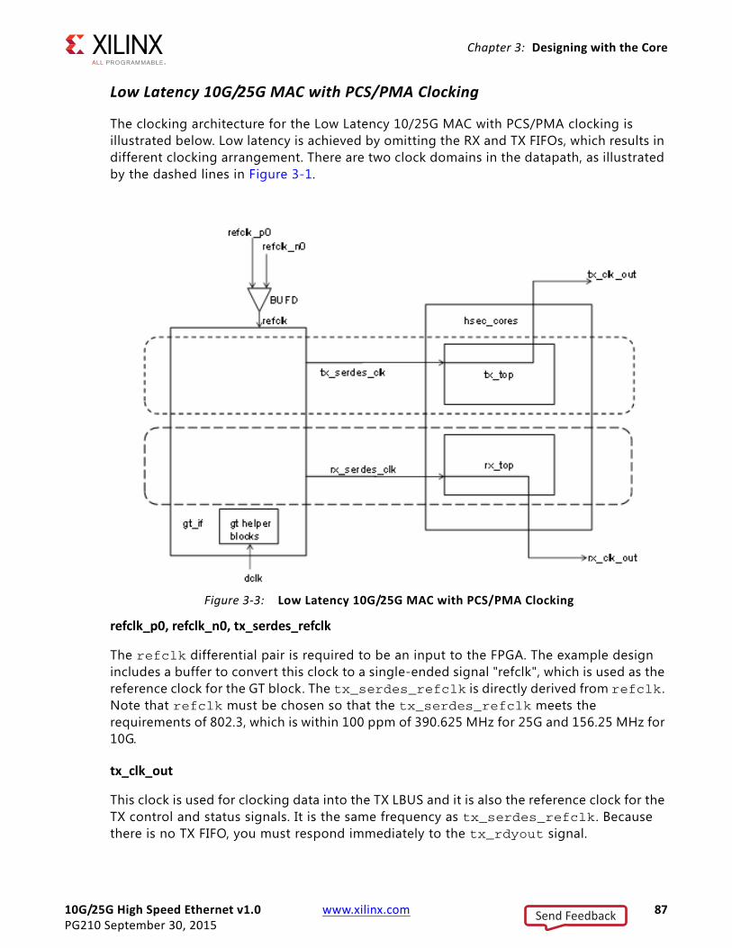
10G/25G High Speed Ethernet v1.0 www.xilinx.com 87PG210 September 30, 2015
Chapter 3: Designing with the Core
Low Latency 10G/25G MAC with PCS/PMA Clocking
The clocking architecture for the Low Latency 10/25G MAC with PCS/PMA clocking is illustrated below. Low latency is achieved by omitting the RX and TX FIFOs, which results in different clocking arrangement. There are two clock domains in the datapath, as illustrated by the dashed lines in Figure 3-1.
refclk_p0, refclk_n0, tx_serdes_refclk
The refclk differential pair is required to be an input to the FPGA. The example design includes a buffer to convert this clock to a single-ended signal "refclk", which is used as the reference clock for the GT block. The tx_serdes_refclk is directly derived from refclk . Note that refclk must be chosen so that the tx_serdes_refclk meets the requirements of 802.3, which is within 100 ppm of 390.625 MHz for 25G and 156.25 MHz for 10G.
tx_clk_out
This clock is used for clocking data into the TX LBUS and it is also the reference clock for the TX control and status signals. It is the same frequency as tx_serdes_refclk . Because there is no TX FIFO, you must respond immediately to the tx_rdyout signal.
X-Ref Target - Figure 3-3
Figure 3‐3: Low Latency 10G/25G MAC with PCS/PMA Clocking
Send Feedback
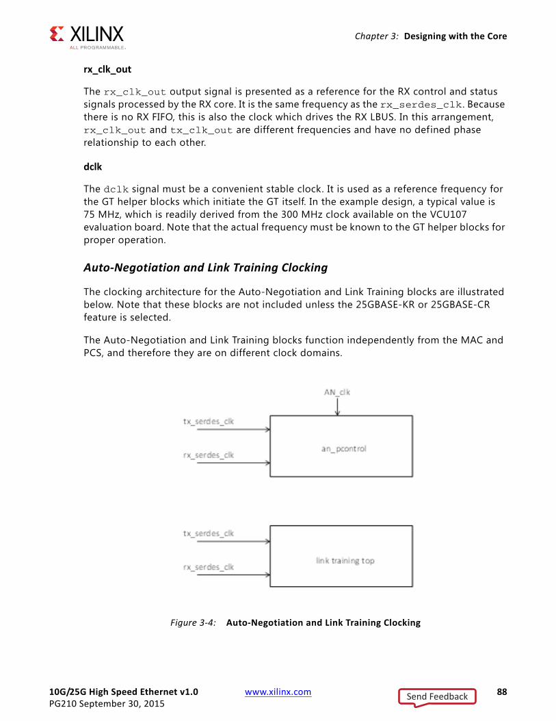
10G/25G High Speed Ethernet v1.0 www.xilinx.com 88PG210 September 30, 2015
Chapter 3: Designing with the Core
rx_clk_out
The rx_clk_out output signal is presented as a reference for the RX control and status signals processed by the RX core. It is the same frequency as the rx_serdes_clk . Because there is no RX FIFO, this is also the clock which drives the RX LBUS. In this arrangement, rx_clk_out and tx_clk_out are different frequencies and have no defined phase relationship to each other.
dclk
The dclk signal must be a convenient stable clock. It is used as a reference frequency for the GT helper blocks which initiate the GT itself. In the example design, a typical value is 75 MHz, which is readily derived from the 300 MHz clock available on the VCU107 evaluation board. Note that the actual frequency must be known to the GT helper blocks for proper operation.
Auto‐Negotiation and Link Training Clocking
The clocking architecture for the Auto-Negotiation and Link Training blocks are illustrated below. Note that these blocks are not included unless the 25GBASE-KR or 25GBASE-CR feature is selected.
The Auto-Negotiation and Link Training blocks function independently from the MAC and PCS, and therefore they are on different clock domains.
X-Ref Target - Figure 3-4
Figure 3‐4: Auto‐Negotiation and Link Training Clocking
Send Feedback
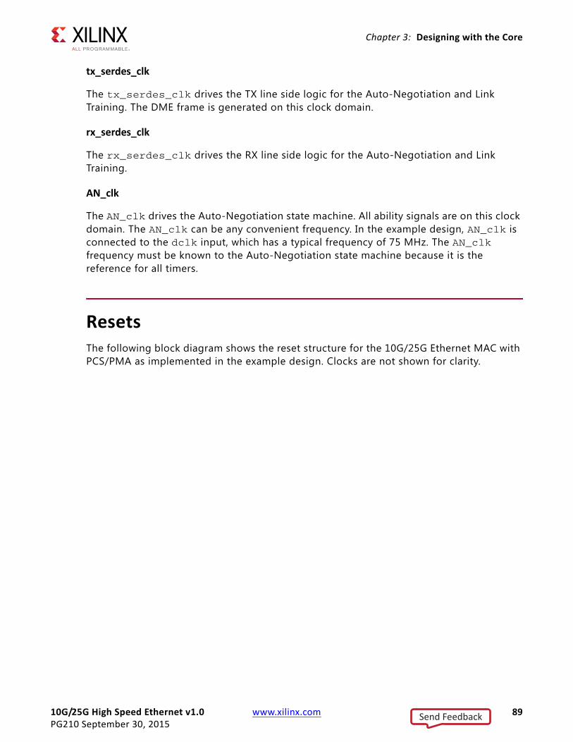
10G/25G High Speed Ethernet v1.0 www.xilinx.com 89PG210 September 30, 2015
Chapter 3: Designing with the Core
tx_serdes_clk
The tx_serdes_clk drives the TX line side logic for the Auto-Negotiation and Link Training. The DME frame is generated on this clock domain.
rx_serdes_clk
The rx_serdes_clk drives the RX line side logic for the Auto-Negotiation and Link Training.
AN_clk
The AN_clk drives the Auto-Negotiation state machine. All ability signals are on this clock domain. The AN_clk can be any convenient frequency. In the example design, AN_clk is connected to the dclk input, which has a typical frequency of 75 MHz. The AN_clk frequency must be known to the Auto-Negotiation state machine because it is the reference for all timers.
ResetsThe following block diagram shows the reset structure for the 10G/25G Ethernet MAC with PCS/PMA as implemented in the example design. Clocks are not shown for clarity.
Send Feedback
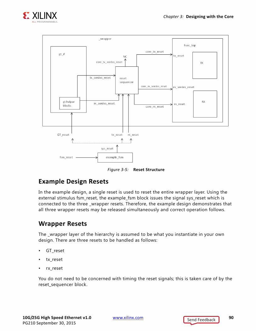
10G/25G High Speed Ethernet v1.0 www.xilinx.com 90PG210 September 30, 2015
Chapter 3: Designing with the Core
Example Design Resets
In the example design, a single reset is used to reset the entire wrapper layer. Using the external stimulus fsm_reset, the example_fsm block issues the signal sys_reset which is connected to the three _wrapper resets. Therefore, the example design demonstrates that all three wrapper resets may be released simultaneously and correct operation follows.
Wrapper Resets
The _wrapper layer of the hierarchy is assumed to be what you instantiate in your own design. There are three resets to be handled as follows:
• GT_reset
• tx_reset
• rx_reset
You do not need to be concerned with timing the reset signals; this is taken care of by the reset_sequencer block.
X-Ref Target - Figure 3-5
Figure 3‐5: Reset Structure
Send Feedback
10G/25G High Speed Ethernet v1.0 www.xilinx.com 91PG210 September 30, 2015
Chapter 3: Designing with the Core
GT_reset
The GT_reset is the asynchronous active High reset input to the GT. You do not need to be concerned with the internal resets of the GT because this is taken care of by the GT helper blocks.
tx_reset
The tx_reset is the asynchronous active High reset for the TX path logic of the 10G/25G Ethernet IP core. While it is connected to the GT reset in the example design, this reset may be asserted at any time to reset the TX path independently without disturbing the RX path.
rx_reset
The rx_reset is the asynchronous active High reset for the RX path logic of the 10G/25G Ethernet IP core. While it is connected to the GT reset in the example design, this reset may be asserted at any time to reset the RX path independently with-out disturbing the TX path.
Connecting the Data Interfaces
LBUS Protocol
The system-side interface of the 10G/25G Ethernet core is a simple packet interface referred to as the LBUS. This section describes the operation of a 64-bit non-segmented LBUS.
The LBUS consists of three separate interfaces:
• Transmitter (TX) interface
• Receiver (RX) interface
• Status/Control interface
The transmitter accepts packet-oriented data, packages the data in accordance with IEEE Std. 802.3 and sends that packaged data to the transceiver macros. The transmitter has control/configuration inputs to shape the data packaging to meet design-specific requirements.
The receiver accepts IEEE Std. 802.3 bitstreams from the transceiver and provides packet-oriented data to the system side.
The Status/Control interface is used to set the characteristics of the interface and to monitor its operation.
The following sections describe the LBUS interfaces. In the descriptions, “asserting” means setting to 1 and “negating” means setting to 0.
Send Feedback
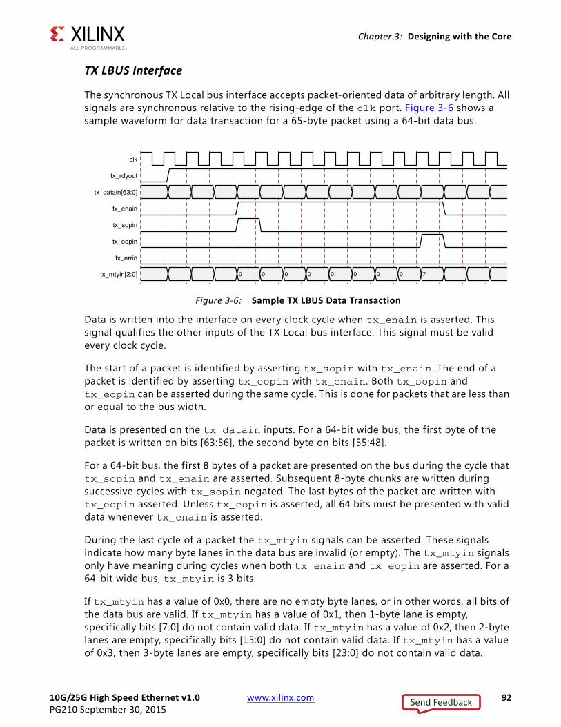
10G/25G High Speed Ethernet v1.0 www.xilinx.com 92PG210 September 30, 2015
Chapter 3: Designing with the Core
TX LBUS Interface
The synchronous TX Local bus interface accepts packet-oriented data of arbitrary length. All signals are synchronous relative to the rising-edge of the clk port. Figure 3-6 shows a sample waveform for data transaction for a 65-byte packet using a 64-bit data bus.
Data is written into the interface on every clock cycle when tx_enain is asserted. This signal qualif ies the other inputs of the TX Local bus interface. This signal must be valid every clock cycle.
The start of a packet is identif ied by asserting tx_sopin with tx_enain. The end of a packet is identif ied by asserting tx_eopin with tx_enain. Both tx_sopin and tx_eopin can be asserted during the same cycle. This is done for packets that are less than or equal to the bus width.
Data is presented on the tx_datain inputs. For a 64-bit wide bus, the f irst byte of the packet is written on bits [63:56], the second byte on bits [55:48].
For a 64-bit bus, the first 8 bytes of a packet are presented on the bus during the cycle that tx_sopin and tx_enain are asserted. Subsequent 8-byte chunks are written during successive cycles with tx_sopin negated. The last bytes of the packet are written with tx_eopin asserted. Unless tx_eopin is asserted, all 64 bits must be presented with valid data whenever tx_enain is asserted.
During the last cycle of a packet the tx_mtyin signals can be asserted. These signals indicate how many byte lanes in the data bus are invalid (or empty). The tx_mtyin signals only have meaning during cycles when both tx_enain and tx_eopin are asserted. For a 64-bit wide bus, tx_mtyin is 3 bits.
If tx_mtyin has a value of 0x0, there are no empty byte lanes, or in other words, all bits of the data bus are valid. If tx_mtyin has a value of 0x1, then 1-byte lane is empty, specifically bits [7:0] do not contain valid data. If tx_mtyin has a value of 0x2, then 2-byte lanes are empty, specif ically bits [15:0] do not contain valid data. If tx_mtyin has a value of 0x3, then 3-byte lanes are empty, specifically bits [23:0] do not contain valid data.
X-Ref Target - Figure 3-6
Figure 3‐6: Sample TX LBUS Data Transaction
Send Feedback
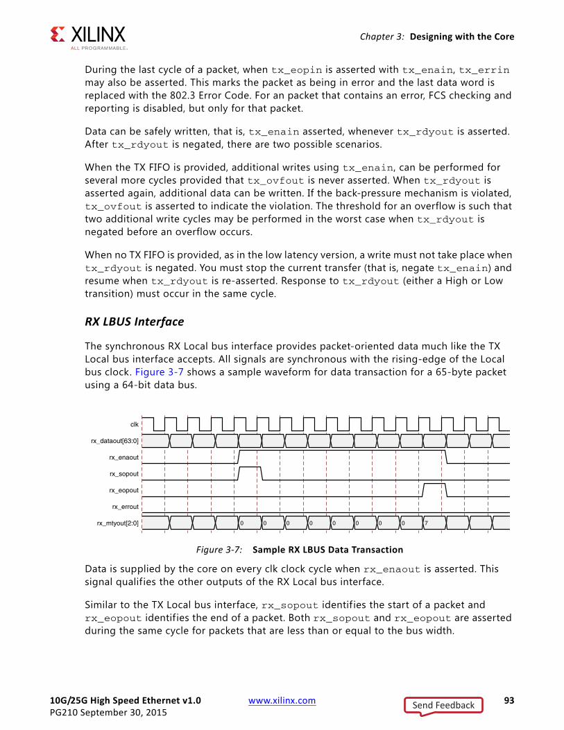
10G/25G High Speed Ethernet v1.0 www.xilinx.com 93PG210 September 30, 2015
Chapter 3: Designing with the Core
During the last cycle of a packet, when tx_eopin is asserted with tx_enain, tx_errin may also be asserted. This marks the packet as being in error and the last data word is replaced with the 802.3 Error Code. For an packet that contains an error, FCS checking and reporting is disabled, but only for that packet.
Data can be safely written, that is, tx_enain asserted, whenever tx_rdyout is asserted. After tx_rdyout is negated, there are two possible scenarios.
When the TX FIFO is provided, additional writes using tx_enain, can be performed for several more cycles provided that tx_ovfout is never asserted. When tx_rdyout is asserted again, additional data can be written. If the back-pressure mechanism is violated, tx_ovfout is asserted to indicate the violation. The threshold for an overflow is such that two additional write cycles may be performed in the worst case when tx_rdyout is negated before an overflow occurs.
When no TX FIFO is provided, as in the low latency version, a write must not take place when tx_rdyout is negated. You must stop the current transfer (that is, negate tx_enain) and resume when tx_rdyout is re-asserted. Response to tx_rdyout (either a High or Low transition) must occur in the same cycle.
RX LBUS Interface
The synchronous RX Local bus interface provides packet-oriented data much like the TX Local bus interface accepts. All signals are synchronous with the rising-edge of the Local bus clock. Figure 3-7 shows a sample waveform for data transaction for a 65-byte packet using a 64-bit data bus.
Data is supplied by the core on every clk clock cycle when rx_enaout is asserted. This signal qualif ies the other outputs of the RX Local bus interface.
Similar to the TX Local bus interface, rx_sopout identif ies the start of a packet and rx_eopout identif ies the end of a packet. Both rx_sopout and rx_eopout are asserted during the same cycle for packets that are less than or equal to the bus width.
X-Ref Target - Figure 3-7
Figure 3‐7: Sample RX LBUS Data Transaction
Send Feedback

10G/25G High Speed Ethernet v1.0 www.xilinx.com 94PG210 September 30, 2015
Chapter 3: Designing with the Core
Similar to the TX Local bus interface, the f irst byte of a packet is supplied on the most signif icant bits of rx_dataout. For a 64-bit wide bus, the f irst byte of the packet is written on bits [63:56], the second byte on bits [55:48].
Similar to the TX Local bus interface, portions of packets are written on the bus in the full width of the bus unless rx_eopout is asserted. When rx_eopout is asserted, the rx_mtyout bus indicates how many byte lanes in the data bus are invalid. The encoding is the same as for tx_mtyin.
During the last cycle of a packet, when rx_eopout is asserted with rx_enaout, rx_errout might also be asserted. This indicates the packet received either had an FCS error, the length was out of the valid range (valid range is least 64 bytes and no more than ctl_rx_max_packet_len[14:0]), or had a bad 64B/66B code that was received during the receipt of the packet.
There is no mechanism to back pressure the RX Local bus interface. Your logic must be capable of receiving data when rx_enaout is asserted.
AXI4‐Stream ProtocolThis section describes how to connect the optional AXI streaming data interfaces of the core. The AXI4-Stream interface may be used instead of the LBUS for the data path.
Transmit AXI4‐Stream Interface
Table 3-1 shows the AXI4-Stream transmit interface signals.
Data Lane Mapping
For transmit data s_axis_tx_tdata, the port is divided into lane 0 to lane 7 (see Table 3-2).
Table 3‐1: AXI4‐Stream Transmit Interface Signals
Signal Direction Description
tx_axis_ tdata[63:0] In AXI4-Stream data (64-bit interface)
tx_axis_ tkeep[7:0] In AXI4-Stream Data Control (64-bit interface)
tx_axis_tvalid In AXI4-Stream Data Valid input
tx_axis_ tuser In AXI4-Stream user signal used to indicate explicit underrun
tx_axis_ tlast In AXI4-Stream signal indicating End of Ethernet Packet. Equivalent to the tx_eop signal on the LBUS.
tx_axis_ tready Out AXI4-Stream acknowledge signal to indicate to start the Data transfer.
Send Feedback

10G/25G High Speed Ethernet v1.0 www.xilinx.com 95PG210 September 30, 2015
Chapter 3: Designing with the Core
Normal Transmission
The timing of a normal frame transfer is shown in Figure 3-8. When the client wants to transmit a frame, it asserts the s_axis_tx_tvalid and places the data and control in s_axis_tx_tdata and s_axis_tx_tkeep in the same clock cycle. When this data is accepted by the core, indicated by s_axis_tx_tready being asserted, the client must provide the next cycle of data. If s_axis_tx_tready is not asserted by the core then the client must hold the current valid data value until it is. The end of packet is indicated to the core by s_axis_tx_tlast asserted for 1 cycle. The bits of s_axis_tx_tkeep are set appropriately to indicate the number of valid bytes in the final data transfer.
After s_axis_tx_tlast is deasserted, any data and control is deemed invalid until s_axis_tx_tvalid is next asserted.
Aborting a Transmission
The aborted transfer of a packet on the client interface is called an underrun. This can happen if a FIFO in the AXI Transmit client interface empties before a frame is completed.
Table 3‐2: s_axis_tx_tdata Lanes
Lane/s_axis_tx_tkeep Bit s_axis_tx_tdata Bits
0 7:0
1 15:8
2 23:16
3 31:24
4 39:32
5 47:40
6 55:48
7 63:56
X-Ref Target - Figure 3-8
Figure 3‐8: Normal Frame Transfer
Send Feedback
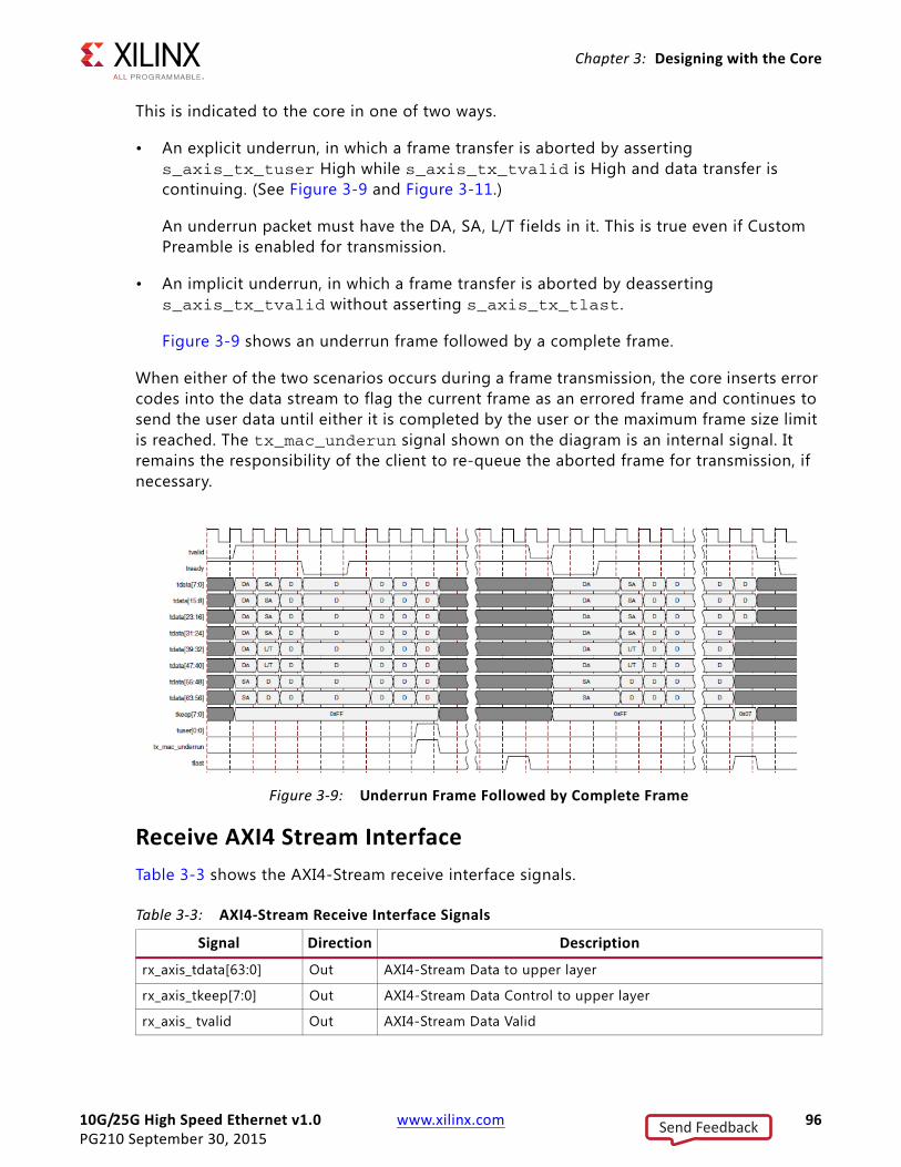
10G/25G High Speed Ethernet v1.0 www.xilinx.com 96PG210 September 30, 2015
Chapter 3: Designing with the Core
This is indicated to the core in one of two ways.
• An explicit underrun, in which a frame transfer is aborted by asserting s_axis_tx_tuser High while s_axis_tx_tvalid is High and data transfer is continuing. (See Figure 3-9 and Figure 3-11.)
An underrun packet must have the DA, SA, L/T fields in it. This is true even if Custom Preamble is enabled for transmission.
• An implicit underrun, in which a frame transfer is aborted by deasserting s_axis_tx_tvalid without asserting s_axis_tx_tlast.
Figure 3-9 shows an underrun frame followed by a complete frame.
When either of the two scenarios occurs during a frame transmission, the core inserts error codes into the data stream to flag the current frame as an errored frame and continues to send the user data until either it is completed by the user or the maximum frame size limit is reached. The tx_mac_underun signal shown on the diagram is an internal signal. It remains the responsibility of the client to re-queue the aborted frame for transmission, if necessary.
Receive AXI4 Stream Interface
Table 3-3 shows the AXI4-Stream receive interface signals.
X-Ref Target - Figure 3-9
Figure 3‐9: Underrun Frame Followed by Complete Frame
Table 3‐3: AXI4‐Stream Receive Interface Signals
Signal Direction Description
rx_axis_tdata[63:0] Out AXI4-Stream Data to upper layer
rx_axis_tkeep[7:0] Out AXI4-Stream Data Control to upper layer
rx_axis_ tvalid Out AXI4-Stream Data Valid
Send Feedback
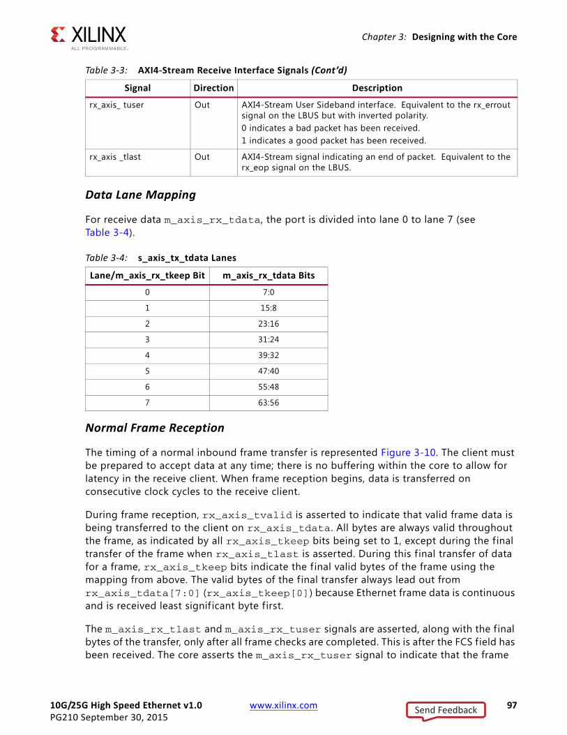
10G/25G High Speed Ethernet v1.0 www.xilinx.com 97PG210 September 30, 2015
Chapter 3: Designing with the Core
Data Lane Mapping
For receive data m_axis_rx_tdata, the port is divided into lane 0 to lane 7 (see Table 3-4).
Normal Frame Reception
The timing of a normal inbound frame transfer is represented Figure 3-10. The client must be prepared to accept data at any time; there is no buffering within the core to allow for latency in the receive client. When frame reception begins, data is transferred on consecutive clock cycles to the receive client.
During frame reception, rx_axis_tvalid is asserted to indicate that valid frame data is being transferred to the client on rx_axis_tdata. All bytes are always valid throughout the frame, as indicated by all rx_axis_tkeep bits being set to 1, except during the f inal transfer of the frame when rx_axis_tlast is asserted. During this f inal transfer of data for a frame, rx_axis_tkeep bits indicate the f inal valid bytes of the frame using the mapping from above. The valid bytes of the f inal transfer always lead out from rx_axis_tdata[7:0] (rx_axis_tkeep[0]) because Ethernet frame data is continuous and is received least signif icant byte first.
The m_axis_rx_tlast and m_axis_rx_tuser signals are asserted, along with the f inal bytes of the transfer, only after all frame checks are completed. This is after the FCS field has been received. The core asserts the m_axis_rx_tuser signal to indicate that the frame
rx_axis_ tuser Out AXI4-Stream User Sideband interface. Equivalent to the rx_errout signal on the LBUS but with inverted polarity.0 indicates a bad packet has been received.1 indicates a good packet has been received.
rx_axis _tlast Out AXI4-Stream signal indicating an end of packet. Equivalent to the rx_eop signal on the LBUS.
Table 3‐4: s_axis_tx_tdata Lanes
Lane/m_axis_rx_tkeep Bit m_axis_rx_tdata Bits
0 7:0
1 15:8
2 23:16
3 31:24
4 39:32
5 47:40
6 55:48
7 63:56
Table 3‐3: AXI4‐Stream Receive Interface Signals (Cont’d)
Signal Direction Description
Send Feedback
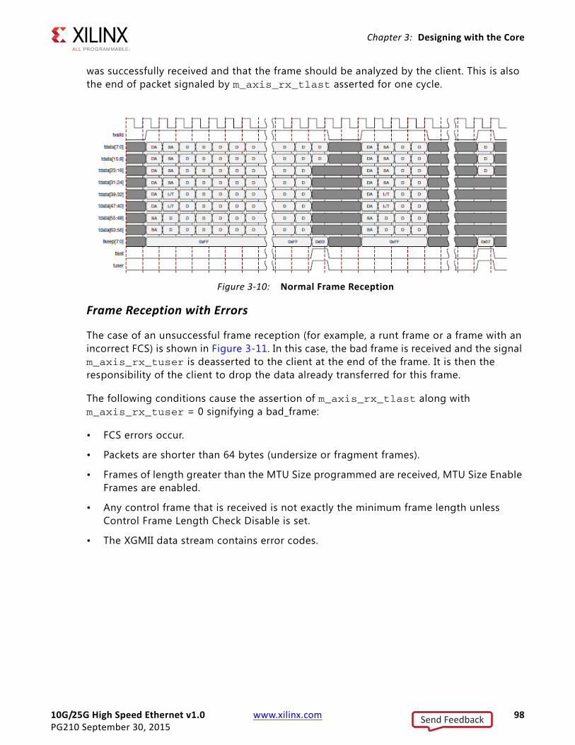
10G/25G High Speed Ethernet v1.0 www.xilinx.com 98PG210 September 30, 2015
Chapter 3: Designing with the Core
was successfully received and that the frame should be analyzed by the client. This is also the end of packet signaled by m_axis_rx_tlast asserted for one cycle.
Frame Reception with Errors
The case of an unsuccessful frame reception (for example, a runt frame or a frame with an incorrect FCS) is shown in Figure 3-11. In this case, the bad frame is received and the signal m_axis_rx_tuser is deasserted to the client at the end of the frame. It is then the responsibility of the client to drop the data already transferred for this frame.
The following conditions cause the assertion of m_axis_rx_tlast along with m_axis_rx_tuser = 0 signifying a bad_frame:
• FCS errors occur.
• Packets are shorter than 64 bytes (undersize or fragment frames).
• Frames of length greater than the MTU Size programmed are received, MTU Size Enable Frames are enabled.
• Any control frame that is received is not exactly the minimum frame length unless Control Frame Length Check Disable is set.
• The XGMII data stream contains error codes.
X-Ref Target - Figure 3-10
Figure 3‐10: Normal Frame Reception
Send Feedback
10G/25G High Speed Ethernet v1.0 www.xilinx.com 99PG210 September 30, 2015
Chapter 3: Designing with the Core
Status/Control InterfaceThe Status/Control interface allows you to set up the 10G/25G Ethernet core configuration and to monitor its status. This sections describes in more detail some of the Status and Control signals.
stat_rx_framing_err and stat_rx_framing_err_valid
These signals are used to keep track of sync header errors. This set of buses is used to keep track of sync header errors. The stat_rx_framing_err output indicates how many sync header errors were received and it is qualif ied (that is, the value is only valid) when the corresponding stat_rx_framing_err_valid is sampled as a 1.
stat_rx_block_lock
This bit indicates that the interface has achieved sync header lock as defined by IEEE Std. 802.3. A value of 1 indicates block lock is achieved.
stat_rx_local_fault
This output is High when stat_rx_internal_local_fault or stat_rx_received_local_fault is asserted. This is output is level sensitive.
X-Ref Target - Figure 3-11
Figure 3‐11: Frame Reception with Errors
Send Feedback
10G/25G High Speed Ethernet v1.0 www.xilinx.com 100PG210 September 30, 2015
Chapter 3: Designing with the Core
RX Error Status
The core provides status signals to identify 64b/66b words and sequences violations and CRC32 checking failures.
All signals are synchronous with the rising-edge of clk and a detailed description of each signal follows.
stat_rx_bad_fcs[1:0]
When this signal is positive, it indicates that the error detection logic has identif ied mismatches between the expected and received value of CRC32 in the received packet.
When a CRC32 error is detected, the received packet is marked as containing an error and is sent with rx_errout asserted during the last transfer (the cycle with rx_eopout asserted), unless ctl_rx_ignore_fcs is asserted. This signal is asserted for one clock period for each CRC32 error detected.
stat_rx_bad_code
This signal indicates how many cycles the RX PCS receive state machine is in the RX_E state as defined by IEEE Std. 802.3.
Pause ProcessingThe 10G/25G Ethernet core provides a comprehensive mechanism for pause packet termination and generation. The TX and RX have independent interfaces for processing pause information as described in this section.
TX Pause Generation
You can request a pause packet to be transmitted using the ctl_tx_pause_req[8:0] and ctl_tx_pause_enable[8:0] input buses. Bit [8] corresponds to global pause packets and bits [7:0] correspond to priority pause packets.
Each bit of this bus must be held at a steady state for a minimum of 16 cycles before the next transition.
CAUTION! Requesting both global and priority pause packets at the same time results in unpredictable behavior and must be avoided.
Send Feedback
10G/25G High Speed Ethernet v1.0 www.xilinx.com 101PG210 September 30, 2015
Chapter 3: Designing with the Core
The contents of the pause packet are determined using the following input pins.
Global pause packets:
ctl_tx_da_gpp[47:0]ctl_tx_sa_gpp[47:0]ctl_tx_ethertype_gpp[15:0]ctl_tx_opcode_gpp[15:0]ctl_tx_pause_quanta8[15:0]
Priority pause packets:
ctl_tx_da_ppp[47:0]ctl_tx_sa_ppp[47:0]ctl_tx_ethertype_ppp[15:0]ctl_tx_opcode_ppp[15:0]ctl_tx_pause_quanta0[15:0]ctl_tx_pause_quanta1[15:0]ctl_tx_pause_quanta2[15:0]ctl_tx_pause_quanta3[15:0]ctl_tx_pause_quanta4[15:0]ctl_tx_pause_quanta5[15:0]ctl_tx_pause_quanta6[15:0]ctl_tx_pause_quanta7[15:0]
The 10G/25G Ethernet core automatically calculates and adds the FCS to the packet. For priority pause packets the 10G/25G Ethernet core also automatically generates the enable vector based on the priorities that are requested.
To request a pause packet, you must set the corresponding bit of the ctl_tx_pause_req[8:0] and ctl_tx_pause_enable[8:0] bus to a 1 and keep it at 1 for the duration of the pause request (that is, if these inputs are set to 0, all pending pause packets are cancelled). The 10G/25G Ethernet core transmits the pause packet immediately after the current packet in flight is completed.
IMPORTANT: Each bit of this bus must be held at a steady state for a minimum of 16 cycles before the next transition.
To retransmit pause packets, the 10G/25G Ethernet core maintains a total of nine independent timers; one for each priority and one for global pause. These timers are loaded with the value of the corresponding input buses. After a pause packet is transmitted the corresponding timer is loaded with the corresponding value of the ctl_tx_pause_refresh_timer[8:0] input bus. When a timer times out, another packet for that priority (or global) is transmitted as soon as the current packet in flight is completed. Additionally, you can manually force the timers to 0, and therefore force a retransmission, by setting the ctl_tx_resend_pause input to 1 for one clock cycle.
To reduce the number of pause packets for priority mode operation, a timer is considered timed out if any of the other timers time out. Additionally, while waiting for the current packet in flight to be completed, any new timer that times out or any new requests are
Send Feedback
10G/25G High Speed Ethernet v1.0 www.xilinx.com 102PG210 September 30, 2015
Chapter 3: Designing with the Core
merged into a single pause frame. For example, if two timers are counting down, and you send a request for a third priority, the two timers are forced to be timed out and a pause packet for all three priorities is sent as soon as the current in-flight packet (if any) is transmitted. Similarly, if one of the two timers times out without an additional request, both timers are forced to be timed out and a pause packet for both priorities is sent as soon as the current in-flight packet (if any) is transmitted.
You can stop pause packet generation by setting the appropriate bits of ctl_tx_pause_req[8:0] or ctl_tx_pause_enable[8:0] to 0.
RX Pause Termination
The 10G/25G Ethernet core terminates global and priority pause frames and provides a simple hand-shaking interface to allow user logic to respond to pause packets.
Determining Pause Packets
There are three steps in determining pause packets:
1. Checks are performed to see if a packet is a global or a priority control packet.
Packets that pass step one are forwarded to you only if ctl_rx_forward_control is set to 1.
2. If step one passes, the packet is checked to determine if it is a global pause packet.
3. If step two fails, the packet is checked to determine if it is a priority pause packet.
For step 1, the following pseudo code shows the checking function:
assign da_match_gcp = (!ctl_rx_check_mcast_gcp && !ctl_rx_check_ucast_gcp) || ((DA == ctl_rx_pause_da_ucast) && ctl_rx_check_ucast_gcp) || ((DA == 48'h0180c2000001) && ctl_rx_check_mcast_gcp);assign sa_match_gcp = !ctl_rx_check_sa_gcp || (SA == ctl_rx_pause_sa);assign etype_match_gcp = !ctl_rx_check_etype_gcp || (ETYPE == ctl_rx_etype_gcp);assign opcode_match_gcp = !ctl_rx_check_opcode_gcp || ((OPCODE >= ctl_rx_opcode_min_gcp) && (OPCODE <= ctl_rx_opcode_max_gcp));assign global_control_packet = da_match_gcp && sa_match_gcp && etype_match_gcp && opcode_match_gcp && ctl_rx_enable_gcp;assign da_match_pcp = (!ctl_rx_check_mcast_pcp && !ctl_rx_check_ucast_pcp) || ((DA == ctl_rx_pause_da_ucast) && ctl_rx_check_ucast_pcp) || ((DA == ctl_rx_pause_da_mcast) && ctl_rx_check_mcast_pcp);assign sa_match_pcp = !ctl_rx_check_sa_pcp || (SA == ctl_rx_pause_sa);assign etype_match_pcp = !ctl_rx_check_etype_pcp || (ETYPE == ctl_rx_etype_pcp);assign opcode_match_pcp = !ctl_rx_check_opcode_pcp || ((OPCODE >= ctl_rx_opcode_min_pcp) && (OPCODE <= ctl_rx_opcode_max_pcp));assign priority_control_packet = da_match_pcp && sa_match_pcp && etype_match_pcp && opcode_match_pcp && ctl_rx_enable_pcp;assign control_packet = global_control_packet || priority_control_packet;
where DA is the destination address, SA is the source address, OPCODE is the opcode and ETYPE is the ethertype/length f ield that are extracted from the incoming packet.
Send Feedback
10G/25G High Speed Ethernet v1.0 www.xilinx.com 103PG210 September 30, 2015
Chapter 3: Designing with the Core
For step 2, the following pseudo code shows the checking function:
assign da_match_gpp = (!ctl_rx_check_mcast_gpp && !ctl_rx_check_ucast_gpp) || ((DA == ctl_rx_pause_da_ucast) && ctl_rx_check_ucast_gpp) || ((DA == 48'h0180c2000001) && ctl_rx_check_mcast_gpp);assign sa_match_gpp = !ctl_rx_check_sa_gpp || (SA == ctl_rx_pause_sa);assign etype_match_gpp = !ctl_rx_check_etype_gpp || (ETYPE == ctl_rx_etype_gpp);assign opcode_match_gpp = !ctl_rx_check_opcode_gpp || (OPCODE == ctl_rx_opcode_gpp);assign global_pause_packet = da_match_gpp && sa_match_gpp && etype_match_gpp && opcode_match_gpp && ctl_rx_enable_gpp;
where DA is the destination address, SA is the source address, OPCODE is the opcode and ETYPE is the ethertype/length f ield that are extracted from the incoming packet.
For step 3, the following pseudo code shows the checking function:
assign da_match_ppp = (!ctl_rx_check_mcast_ppp && !ctl_rx_check_ucast_ppp) || ((DA == ctl_rx_pause_da_ucast) && ctl_rx_check_ucast_ppp) || ((DA == ctl_rx_pause_da_mcast) && ctl_rx_check_mcast_ppp);assign sa_match_ppp = !ctl_rx_check_sa_ppp || (SA == ctl_rx_pause_sa);assign etype_match_ppp = !ctl_rx_check_etype_ppp || (ETYPE == ctl_rx_etype_ppp);assign opcode_match_ppp = !ctl_rx_check_opcode_ppp || (OPCODE == ctl_rx_opcode_ppp);assign priority_pause_packet = da_match_ppp && sa_match_ppp && etype_match_ppp && opcode_match_ppp && ctl_rx_enable_ppp;
where DA is the destination address, SA is the source address, OPCODE is the opcode and ETYPE is the ethertype/length f ield that are extracted from the incoming packet.
User Interface
A simple hand-shaking protocol is used to alert you of the reception of pause packets using the ctl_rx_pause_enable[8:0], stat_rx_pause_req[8:0] and ctl_rx_pause_ack[8:0] buses. For these buses, bit [8] corresponds to global pause packets and bits [7:0] correspond to priority pause packets.
The following steps occur when a pause packet is received:
1. If the corresponding bit of ctl_rx_pause_enable[8:0] is 0, the quanta is ignored and the hard CMAC stays in step 1. Otherwise, the corresponding bit of the stat_rx_pause_req[8:0] bus is set to 1, and the received quanta is loaded into a timer.
If one of the bits of ctl_rx_pause_enable[8:0] is set to 0 (disabled) when the pause processing is in step 2 or later, the core completes the steps as normal until it comes back to step 1.
2. If ctl_rx_check_ack input is 1, the core waits for you to set the appropriate bit of the ctl_rx_pause_ack[8:0] bus to 1.
3. After you set the proper bit of ctl_rx_pause_ack[8:0] to 1, or if ctl_rx_check_ack is 0, the core starts counting down the timer.
Send Feedback
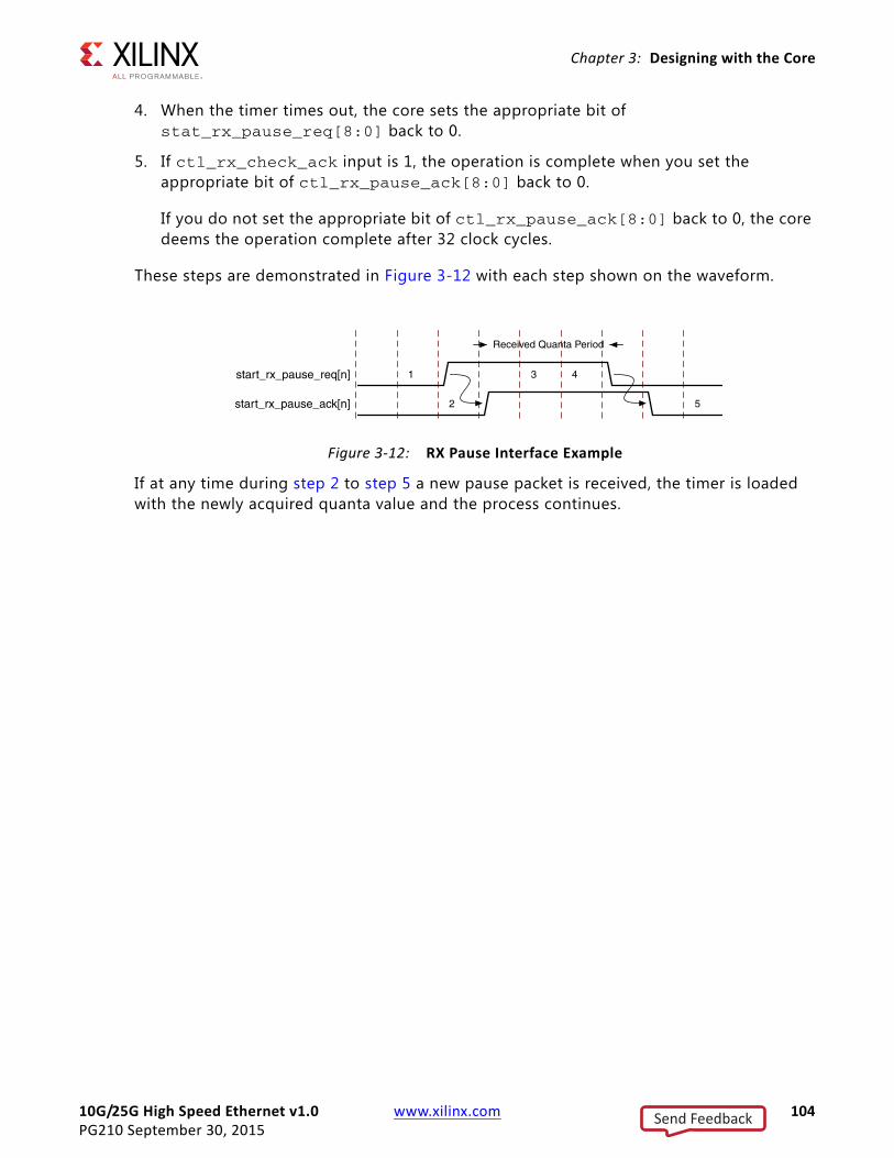
10G/25G High Speed Ethernet v1.0 www.xilinx.com 104PG210 September 30, 2015
Chapter 3: Designing with the Core
4. When the timer times out, the core sets the appropriate bit of stat_rx_pause_req[8:0] back to 0.
5. If ctl_rx_check_ack input is 1, the operation is complete when you set the appropriate bit of ctl_rx_pause_ack[8:0] back to 0.
If you do not set the appropriate bit of ctl_rx_pause_ack[8:0] back to 0, the core deems the operation complete after 32 clock cycles.
These steps are demonstrated in Figure 3-12 with each step shown on the waveform.
If at any time during step 2 to step 5 a new pause packet is received, the timer is loaded with the newly acquired quanta value and the process continues.
X-Ref Target - Figure 3-12
Figure 3‐12: RX Pause Interface Example
Send Feedback
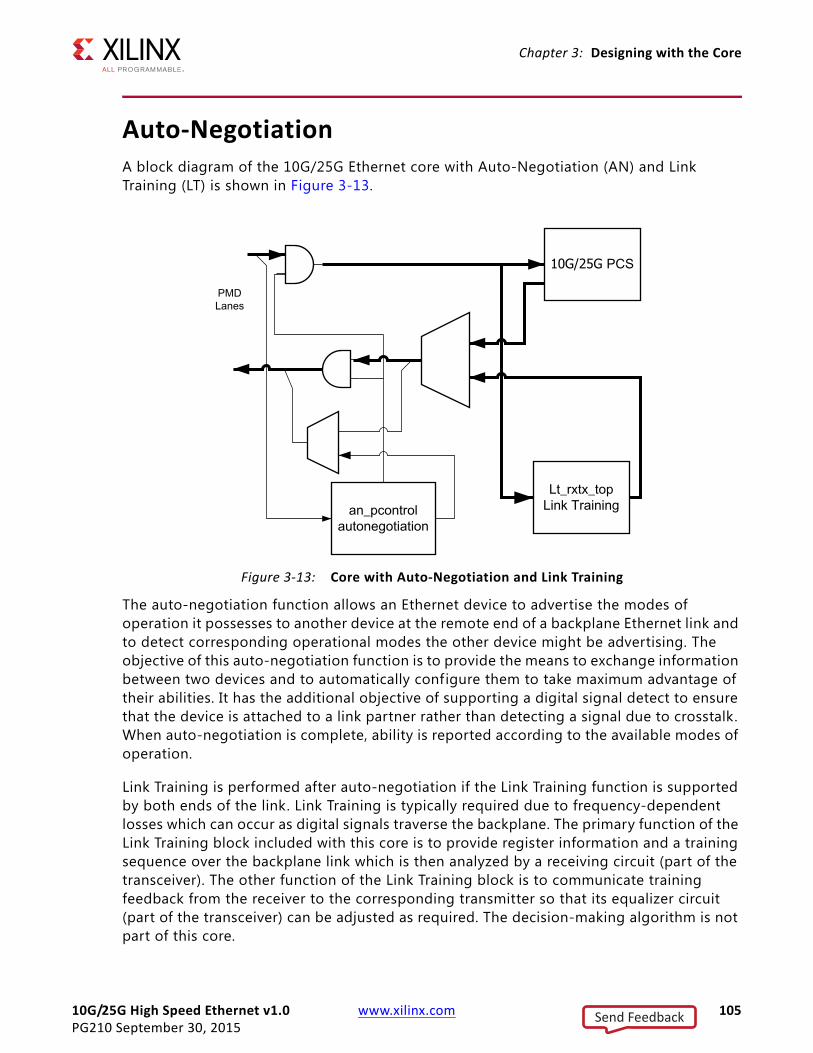
10G/25G High Speed Ethernet v1.0 www.xilinx.com 105PG210 September 30, 2015
Chapter 3: Designing with the Core
Auto‐NegotiationA block diagram of the 10G/25G Ethernet core with Auto-Negotiation (AN) and Link Training (LT) is shown in Figure 3-13.
The auto-negotiation function allows an Ethernet device to advertise the modes of operation it possesses to another device at the remote end of a backplane Ethernet link and to detect corresponding operational modes the other device might be advertising. The objective of this auto-negotiation function is to provide the means to exchange information between two devices and to automatically configure them to take maximum advantage of their abilities. It has the additional objective of supporting a digital signal detect to ensure that the device is attached to a link partner rather than detecting a signal due to crosstalk. When auto-negotiation is complete, ability is reported according to the available modes of operation.
Link Training is performed after auto-negotiation if the Link Training function is supported by both ends of the link. Link Training is typically required due to frequency-dependent losses which can occur as digital signals traverse the backplane. The primary function of the Link Training block included with this core is to provide register information and a training sequence over the backplane link which is then analyzed by a receiving circuit (part of the transceiver). The other function of the Link Training block is to communicate training feedback from the receiver to the corresponding transmitter so that its equalizer circuit (part of the transceiver) can be adjusted as required. The decision-making algorithm is not part of this core.
X-Ref Target - Figure 3-13
Figure 3‐13: Core with Auto‐Negotiation and Link Training
Send Feedback

10G/25G High Speed Ethernet v1.0 www.xilinx.com 106PG210 September 30, 2015
Chapter 3: Designing with the Core
When auto-negotiation and Link Training are complete, the datapath is switched to mission mode (the PCS), as shown in Figure 3-13.
Overview
Figure 3-14 shows the position of the auto-negotiation function in the OSI reference model.
The Auto-Negotiation Intellectual Property Core (ANIPC) implements the requirements as specified in Clause 73, IEEE Std 802.3-2012, including those amendments specif ied in IEEE Std. P802.3ba and 802.3ap.
The functions of the ANIPC core are listed in clause 73, specif ically Figure 73-11, Arbitration state diagram, in section 73.10.4, State Diagrams.
During normal mission mode operation, with link control outputs set to (bin)11, the bit operating frequency of the transceiver input and output is typically 10.3125 or 25.78125 Gb/s. However, the DME bit rate used on the lane during Auto-Negotiation is different to the mission mode operation. To accommodate this requirement, the ANIPC core uses over-sampling and over driving to match the 156.25 Mb/s Auto-Negotiation speed (DME clock frequency 312.5 MHz) with the mission mode 10.3125 or 25.78125 Gb/s physical lane speed.
Functional Description
autoneg_enable
When the autoneg_enable input signal is set to 1, auto-negotiation begins automatically at power-up, or if the carrier signal is lost, or if the input restart_negotiation signal is cycled from a 0 to a 1. All of the Ability input signals as well as the two input signals PAUSE
X-Ref Target - Figure 3-14
Figure 3‐14: Auto‐Negotiation Function in the OSI Model
Send Feedback
10G/25G High Speed Ethernet v1.0 www.xilinx.com 107PG210 September 30, 2015
Chapter 3: Designing with the Core
and ASM_DIR are tied Low or High to indicate the capability of the hardware. The nonce_seed[7:0] input must be set to a unique non-zero value for every instance of the auto-negotiator. This is important to guarantee that no dead-locks occur at power-up. If two link partners connected together attempt to auto-negotiate with their nonce_seed[7:0] inputs set to the same value, then the auto-negotiation fails continuously. The pseudo_sel input is an arbitrary selection that is used to select the polynomial of the random bit generator used in bit position 49 of the DME pages used during auto-negotiation. Any selection on this input is valid and does not result in any adverse behavior.
Link Control
When auto-negotiation begins, the various link control signals are activated, depending on the disposition of the corresponding Ability inputs for those links. Subsequently, the corresponding link status signals are monitored by the ANIPC hardware for an indication of the state of the various links that are connected. If particular links are unused, then the corresponding link control outputs are unconnected, and the corresponding link-status inputs should be tied Low. During this time, the ANIPC hardware sets up a communication link with the link partner and uses this link to negotiate the capabilities of the connection.
Autoneg Complete
When Auto-Negotiation is complete, the autoneg_complete output signal is asserted. In addition, the output signal an_fec_enable is asserted if the Fowrard Error Correction hardware is to be used, the output signal tx_pause_en is asserted if the transmitter hardware is allowed to generate PAUSE control packets, the output signal rx_pause_en is asserted if the receiver hardware is allowed to detect PAUSE control packets, and the output link control of the selected link is set to its mission mode value (bin)11.
Link TrainingLink Training is performed after Auto Negotiation converges to a backplane or copper technology. Technology selection can also be the result of a manual entry or parallel detection. Link training might be required due to frequency-dependent losses which can occur as digital signals traverse the backplane or a copper cable. The primary function of the Link Training core is to provide register information and a training sequence over the backplane link which is then analyzed by a receiving circuit which is not part of the core. The other function of the core is to communicate training feedback from the receiver to the corresponding transmitter so that its equalizer circuit (not part of the core) can be adjusted as required. The two circuits comprising the core are the receive Link Training block and the transmit Link Training block.
IMPORTANT: The logic responsible for adjusting the transmitter pre-emphasis taps must be supplied external to this IP core.
Send Feedback

10G/25G High Speed Ethernet v1.0 www.xilinx.com 108PG210 September 30, 2015
Chapter 3: Designing with the Core
Functional Description
Transmit
The Link Training transmit block constructs a 4,384-bit frame which contains a frame delimiter, control channel, and link training sequence. It is formatted as shown in Figure 3-15.
Xilinx recommends that the control channel bits not be changed by the Link Training algorithm while the transmit state machine is in the process of transmitting them, or they may be received incorrectly, possibly resulting in a DME error. This time begins when tx_SOF is asserted and ends at least 288 bit times later, or approximately 30 ns.
Although the coeff icient and status contain 128 bit times at the line rate, the actual signaling rate for these two fields is reduced by a factor of 8. Therefore the DME clock rate is one quarter of the line rate.
Frame Marker
The frame marker consists of 16 consecutive 1s followed by 16 consecutive 0s. This pattern is not repeated in the remainder of the frame.
Coefficient and Status
Because the DME signaling rate for these two f ields is reduced by a factor of 8, each coeff icient and status transmission contain 128/8=16 bits each numbered from 15:0. Table 3-5 and Table 3-6 define these bits in the order in which they are transmitted starting with bit 15 and ending with bit 0.
X-Ref Target - Figure 3-15
Figure 3‐15: Link Training Frame Structure
Send Feedback
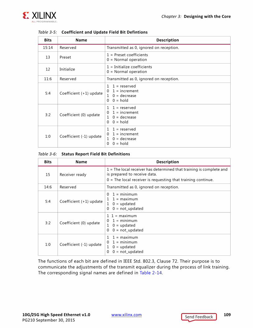
10G/25G High Speed Ethernet v1.0 www.xilinx.com 109PG210 September 30, 2015
Chapter 3: Designing with the Core
The functions of each bit are defined in IEEE Std. 802.3, Clause 72. Their purpose is to communicate the adjustments of the transmit equalizer during the process of link training. The corresponding signal names are defined in Table 2-14.
Table 3‐5: Coefficient and Update Field Bit Defintions
Bits Name Description
15:14 Reserved Transmitted as 0, ignored on reception.
13 Preset 1 = Preset coeff icients0 = Normal operation
12 Initialize 1 = Initialize coefficients0 = Normal operation
11:6 Reserved Transmitted as 0, ignored on reception.
5:4 Coefficient (+1) update
1 1 = reserved0 1 = increment1 0 = decrease 0 0 = hold
3:2 Coefficient (0) update
1 1 = reserved0 1 = increment1 0 = decrease0 0 = hold
1:0 Coefficient (-1) update
1 1 = reserved0 1 = increment1 0 = decrease0 0 = hold
Table 3‐6: Status Report Field Bit Definitions
Bits Name Description
15 Receiver ready1 = The local receiver has determined that training is complete and is prepared to receive data. 0 = The local receiver is requesting that training continue.
14:6 Reserved Transmitted as 0, ignored on reception.
5:4 Coefficient (+1) update
0 1 = minimum1 1 = maximum1 0 = updated0 0 = not_updated
3:2 Coefficient (0) update
1 1 = maximum0 1 = minimum1 0 = updated0 0 = not_updated
1:0 Coefficient (-1) update
1 1 = maximum0 1 = minimum1 0 = updated0 0 = not_updated
Send Feedback
10G/25G High Speed Ethernet v1.0 www.xilinx.com 110PG210 September 30, 2015
Chapter 3: Designing with the Core
Training Sequence
The training sequence consists of a PRBS (pseudo-random bit sequence) of 4094 bits followed by two zeros, for a total of 4096 bits. The PRBS is transmitted at the line rate of 10.3125 or 25.78125 Gb/s. The PRBS generator receives an 11-bit seed from an external source. Subsequent to the initial seed being loaded, the PRBS generator continues to run with no further intervention being required.
The PRBS generator itself is implemented with a circuit which corresponds to the following polynomial:
G(x) = 1 + x9 + x11
Receive
The receive block implements the frame alignment state diagram shown in IEEE Std. 802.3, Clause 72, Figure 72-4.
Frame Lock State Machine
The frame lock state machine searches for the frame marker, consisting of 16 consecutive 1s followed by 16 consecutive 0s. This functionality is fully specif ied in IEEE Std. 802.3, Clause 72, Fig. 72-4. When frame lock has been achieved, frame_lock is set to a value of TRUE.
Received Data
The receiver outputs the control channel with the bit definitions defined in Table 3-5 and Table 3-6 and signal names defined in Port Descriptions.
If a DME error has occurred during the reception of a particular DME frame, the control channel outputs are not updated but retain the value of the last received good DME frame and are updated when the next good DME frame is received.
Send Feedback
10G/25G High Speed Ethernet v1.0 www.xilinx.com 111PG210 September 30, 2015
Chapter 4
Design Flow StepsThis chapter describes customizing and generating the core, constraining the core, and the simulation, synthesis and implementation steps that are specific to this core. More detailed information about the standard Vivado® design flows and the Vivado IP integrator can be found in the following Vivado Design Suite user guides:
• Vivado Design Suite User Guide: Designing IP Subsystems using IP Integrator (UG994) [Ref 4]
• Vivado Design Suite User Guide: Designing with IP (UG896) [Ref 5]
• Vivado Design Suite User Guide: Getting Started (UG910) [Ref 6]
• Vivado Design Suite User Guide: Logic Simulation (UG900) [Ref 7]
Customizing and Generating the CoreThis section includes information about using Xilinx tools to customize and generate the core in the Vivado Design Suite.
If you are customizing and generating the core in the Vivado IP integrator, see the Vivado Design Suite User Guide: Designing IP Subsystems using IP Integrator (UG994) [Ref 4] for detailed information. IP integrator might auto-compute certain configuration values when validating or generating the design. To check whether the values do change, see the description of the parameter in this chapter. To view the parameter value, run the validate_bd_design command in the Tcl console.
You can customize the IP for use in your design by specifying values for the various parameters associated with the core using the following steps:
1. Select the IP from the IP catalog.
2. Double-click the selected IP or select the Customize IP command from the toolbar or right-click menu.
For details, see the Vivado Design Suite User Guide: Designing with IP (UG896) [Ref 5] and the Vivado Design Suite User Guide: Getting Started (UG910) [Ref 6].
Note: Figures in this chapter are illustrations of the Vivado IDE. The layout depicted here might vary from the current version.
Send Feedback
10G/25G High Speed Ethernet v1.0 www.xilinx.com 112PG210 September 30, 2015
Chapter 4: Design Flow Steps
Output Generation
For details, see the Vivado Design Suite User Guide: Designing with IP (UG896) [Ref 5].
Constraining the CoreThis section contains information about constraining the core in the Vivado Design Suite.
Required Constraints
This section is not applicable for this core.
Device, Package, and Speed Grade Selections
This section is not applicable for this core.
Clock Frequencies
This section is not applicable for this core.
Clock Management
This section is not applicable for this core.
Clock Placement
This section is not applicable for this core.
Banking
This section is not applicable for this core.
Transceiver Placement
This section is not applicable for this core.
I/O Standard and Placement
This section is not applicable for this core.
Send Feedback
10G/25G High Speed Ethernet v1.0 www.xilinx.com 113PG210 September 30, 2015
Chapter 4: Design Flow Steps
SimulationThis section contains information about simulating IP in the Vivado Design Suite. For comprehensive information about Vivado simulation components, as well as information about using supported third-party tools, see the Vivado Design Suite User Guide: Logic Simulation (UG900) [Ref 7]. IMPORTANT: For cores targeting 7 series or Zynq-7000 devices, UNIFAST libraries are not supported.
Xilinx IP is tested and qualified with UNISIM libraries only.
Synthesis and ImplementationThis section contains information about synthesis and implementation in the Vivado Design Suite. For details about synthesis and implementation, see the Vivado Design Suite User Guide: Designing with IP (UG896) [Ref 5].
Send Feedback
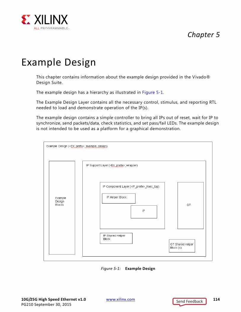
10G/25G High Speed Ethernet v1.0 www.xilinx.com 114PG210 September 30, 2015
Chapter 5
Example DesignThis chapter contains information about the example design provided in the Vivado® Design Suite.
The example design has a hierarchy as illustrated in Figure 5-1.
The Example Design Layer contains all the necessary control, stimulus, and reporting RTL needed to load and demonstrate operation of the IP(s).
The example design contains a simple controller to bring all IPs out of reset, wait for IP to synchronize, send packets/data, check statistics, and set pass/fail LEDs. The example design is not intended to be used as a platform for a graphical demonstration.
X-Ref Target - Figure 5-1
Figure 5‐1: Example Design
Send Feedback
10G/25G High Speed Ethernet v1.0 www.xilinx.com 115PG210 September 30, 2015
Chapter 5: Example Design
Figure 5-1 references the two name prefixes: EX_prefix and IP_prefix. These prefixes are appended to the beginning of all the module names associated with the corresponding design components. This allows easier identif ication of the component parts. Each prefix is unique. As shown in Figure 5-1, the prefix EX_prefix is applied to all of the modules contained in the Example Design layer and in the IP Support Layer. The prefix IP_prefix is applied to all of the module definitions within the IP Component Layer.
The Component Layer
The IP wrapper level of hierarchy is the IP Component Layer (CL). This level is the 'basic unit' instanced by a user wishing stand-alone IP core without any transceiver or shared logic connections. This level contains all the RTL helper blocks necessary to manage the base-IP, and includes the IP (encrypted). You do not need to edit this layer.
Specif ic IP helper blocks such as reset-sequencers are present at this layer.
The Support Layer (Wrapper)
The IP Component Support Layer (CSL) is a wrapper level which contains the base IP plus complete GT. This layer is created to specifically allow n x IP component layers to be instanced and share a common GT blocks. An example would be 4 x 10G/25G Ethernet IP components sharing a single GTY quad and GT shared logic. This layer is instanced as-is and does not need any edits.
In the diagram the GT and GT Shared Helper block RTL is instanced "as-is" from the GT wizard. The blocks combine all the RTL needed to support the GT interface and connection to the IP.
Multiple component layers can be present in this layer. To support these multiple cores, IP shared logic (for example PLL, BUFG) may be present at this layer. Each component layer that is present at this layer has its own unique IP_prefix appended to the beginning of each module definition within the respective component.
Hardware Testing
The board type supported for this test is the VCU107 board. The prerequisite is an on-card reference clock generator, and, for PCS only designs, an MII clock generator. All of the example designs provided are targeted to the specif ic evaluation board, that is, to the VCU107 board. In other words, the device type matches that on the evaluation board, and all of the physical constraints required, most notably, pin numbers for required signals, match the wiring of the specif ic evaluation board.
The example design test is provided as an automatic process. That is, when the BIT file is loaded onto the evaluation board, a test controller module automatically programs the reference clock frequency, reset the IP and the GT, using all the correct reset sequences,
Send Feedback
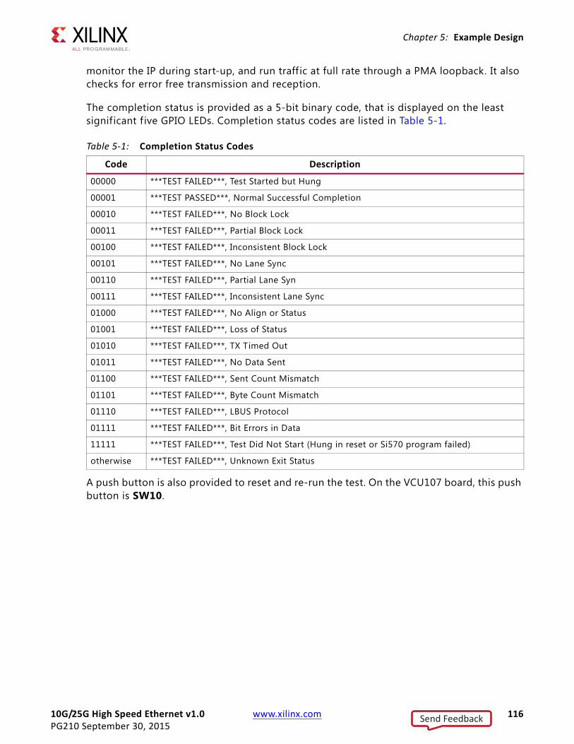
10G/25G High Speed Ethernet v1.0 www.xilinx.com 116PG210 September 30, 2015
Chapter 5: Example Design
monitor the IP during start-up, and run traff ic at full rate through a PMA loopback. It also checks for error free transmission and reception.
The completion status is provided as a 5-bit binary code, that is displayed on the least signif icant f ive GPIO LEDs. Completion status codes are listed in Table 5-1.
A push button is also provided to reset and re-run the test. On the VCU107 board, this push button is SW10.
Table 5‐1: Completion Status Codes
Code Description
00000 ***TEST FAILED***, Test Started but Hung
00001 ***TEST PASSED***, Normal Successful Completion
00010 ***TEST FAILED***, No Block Lock
00011 ***TEST FAILED***, Partial Block Lock
00100 ***TEST FAILED***, Inconsistent Block Lock
00101 ***TEST FAILED***, No Lane Sync
00110 ***TEST FAILED***, Partial Lane Syn
00111 ***TEST FAILED***, Inconsistent Lane Sync
01000 ***TEST FAILED***, No Align or Status
01001 ***TEST FAILED***, Loss of Status
01010 ***TEST FAILED***, TX Timed Out
01011 ***TEST FAILED***, No Data Sent
01100 ***TEST FAILED***, Sent Count Mismatch
01101 ***TEST FAILED***, Byte Count Mismatch
01110 ***TEST FAILED***, LBUS Protocol
01111 ***TEST FAILED***, Bit Errors in Data
11111 ***TEST FAILED***, Test Did Not Start (Hung in reset or Si570 program failed)
otherwise ***TEST FAILED***, Unknown Exit Status
Send Feedback
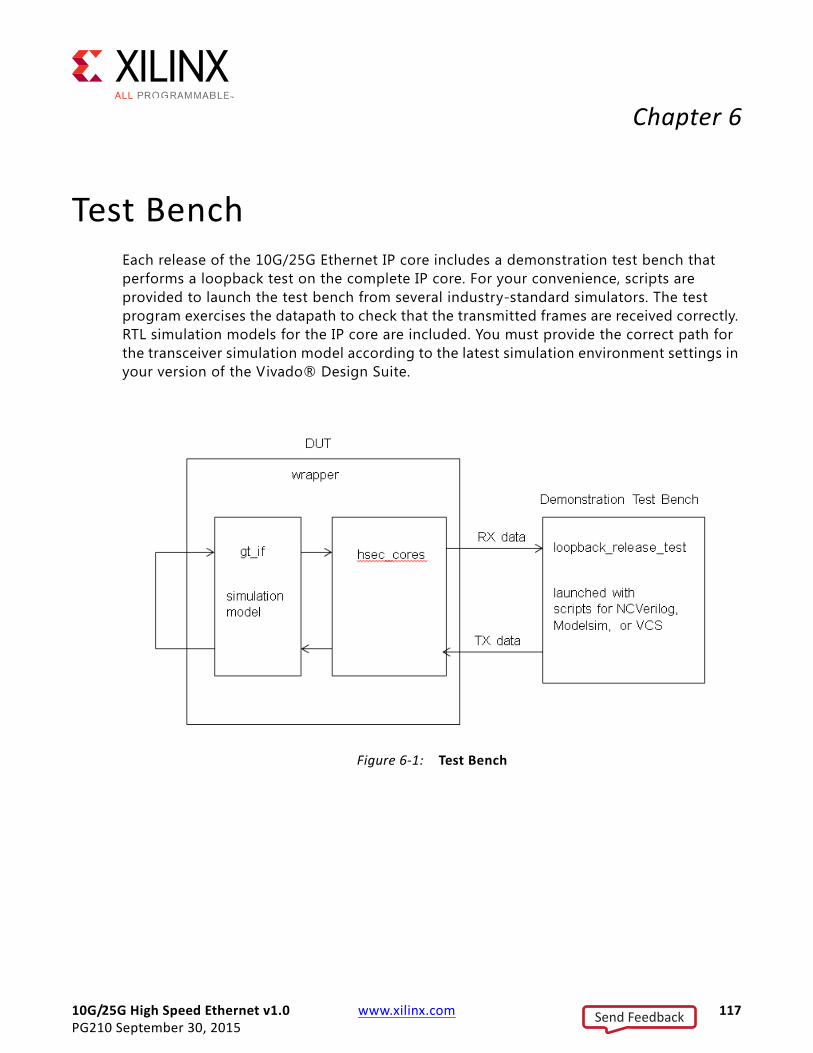
10G/25G High Speed Ethernet v1.0 www.xilinx.com 117PG210 September 30, 2015
Chapter 6
Test BenchEach release of the 10G/25G Ethernet IP core includes a demonstration test bench that performs a loopback test on the complete IP core. For your convenience, scripts are provided to launch the test bench from several industry-standard simulators. The test program exercises the datapath to check that the transmitted frames are received correctly. RTL simulation models for the IP core are included. You must provide the correct path for the transceiver simulation model according to the latest simulation environment settings in your version of the Vivado® Design Suite.
X-Ref Target - Figure 6-1
Figure 6‐1: Test Bench
Send Feedback

10G/25G High Speed Ethernet v1.0 www.xilinx.com 118PG210 September 30, 2015
Appendix A
Migrating and UpgradingThis appendix contains information about migrating a design from the ISE® Design Suite to the Vivado® Design Suite, and for upgrading to a more recent version of the core. For customers upgrading in the Vivado Design Suite, important details (where applicable) about any port changes and other impact to user logic are included.
Upgrading in the Vivado Design SuiteThis section provides information about any changes to the user logic or port designations that take place when you upgrade to a more current version of this core in the Vivado Design Suite.
A script is provided for upgrading the design to a more recent version of Vivado. It is found in the /compile/xilinx/upgrade_IP directory. Run this script to upgrade the transceiver wrapper to the latest version. This should also be done if you want to use the latest transceiver simulation model or you may get simulation errors. Be sure to retain a copy of the original design in the event that you need to revert to the previous version.
Send Feedback
10G/25G High Speed Ethernet v1.0 www.xilinx.com 119PG210 September 30, 2015
Appendix B
DebuggingThis appendix includes details about resources available on the Xilinx Support website and debugging tools.
TIP: If the IP generation halts with an error, there might be a license issue. See License Checkers in Chapter 1 for more details.
Finding Help on Xilinx.comTo help in the design and debug process when using the 10G/25G Ethernet, the Xilinx Support web page contains key resources such as product documentation, release notes, answer records, information about known issues, and links for obtaining further product support.
Documentation
This product guide is the main document associated with the 10G/25G Ethernet. This guide, along with documentation related to all products that aid in the design process, can be found on the Xilinx Support web page or by using the Xilinx Documentation Navigator.
Download the Xilinx Documentation Navigator from the Design Tools tab on the Downloads page. For more information about this tool and the features available, open the online help after installation.
Solution Centers
See the Xilinx Solution Centers for support on devices, software tools, and intellectual property at all stages of the design cycle. Topics include design assistance, advisories, and troubleshooting tips.
The Solution Center specif ic to the 10G/25G Ethernet core is listed below.
• Xilinx Ethernet IP Solution Center
Send Feedback

10G/25G High Speed Ethernet v1.0 www.xilinx.com 120PG210 September 30, 2015
Appendix B: Debugging
Answer Records
Answer Records include information about commonly encountered problems, helpful information on how to resolve these problems, and any known issues with a Xilinx product. Answer Records are created and maintained daily ensuring that users have access to the most accurate information available.
Answer Records for this core can be located by using the Search Support box on the main Xilinx support web page. To maximize your search results, use proper keywords such as
• Product name
• Tool message(s)
• Summary of the issue encountered
A filter search is available after results are returned to further target the results.
Master Answer Record for the 10G/25G Ethernet
AR: 64710
Technical Support
Xilinx provides technical support in the Xilinx Support web page for this LogiCORE™ IP product when used as described in the product documentation. Xilinx cannot guarantee timing, functionality, or support if you do any of the following:
• Implement the solution in devices that are not defined in the documentation.
• Customize the solution beyond that allowed in the product documentation.
• Change any section of the design labeled DO NOT MODIFY.
To contact Xilinx Technical Support, Debug Tools
There are many tools available to address 10G/25G Ethernet design issues. It is important to know which tools are useful for debugging various situations.
Vivado Design Suite Debug Feature
The Vivado® Design Suite debug feature inserts logic analyzer and virtual I/O cores directly into your design. The debug feature also allows you to set trigger conditions to capture application and integrated block port signals in hardware. Captured signals can then be analyzed. This feature in the Vivado IDE is used for logic debugging and validation of a design running in Xilinx devices.
The Vivado logic analyzer is used with the logic debug IP cores, including:
• ILA 2.0 (and later versions)
Send Feedback

10G/25G High Speed Ethernet v1.0 www.xilinx.com 121PG210 September 30, 2015
Appendix B: Debugging
• VIO 2.0 (and later versions)
See the Vivado Design Suite User Guide: Programming and Debugging (UG908) [Ref 8].
Reference Boards
Various Xilinx development boards support the 10G/25G Ethernet. These boards can be used to prototype designs and establish that the core can communicate with the system.
• UltraScale™ FPGA evaluation boards
° VCU107
° VCU108
Simulation DebugEach 10/25G IP core release includes a sample simulation test bench. This consists of a loopback from the TX side of the user interface, through the TX circuit, looping back to the RX circuit, and checking the received packets at the RX side of the user interface.
Each release includes a sample instantiation of a Xilinx transceiver corresponding to the device selected by the customer. The loopback simulation includes a path through the transceiver.
The simulation is run using provided scripts for several common industry-standard simulators.
If the simulation does not run properly from the scripts, the following items should be checked.
Simulator License Availability
If the simulator does not launch, then you may not have a valid license. Ensure that the license is up to date. It is also possible that your organization has a license available for one of the other simulators, so try all the provided scripts.
Library File Location
Each simulation script calls up the required Xilinx library f iles. These are called by the corresponding liblist* f ile in the bin directory of each release.
There may be an error message indicating that the simulator is unable to find certain library files. In this case, the path to the library f iles may have to be modified. Check with your IT administrator to ensure that the paths are correct.
Send Feedback
10G/25G High Speed Ethernet v1.0 www.xilinx.com 122PG210 September 30, 2015
Appendix B: Debugging
Version Compatibility
Each release has been tested according the Xilinx tools version requested by the customer. If the simulation does not complete successfully, you should f irst ensure that a properly up-to-date version of the Xilinx tools is used. The preferred version is indicated in the README file of the release, and is also indicated in the simulation sample log f ile included with the release.
Slow Simulation
Simulations may appear to run slowly under some circumstances. If a simulation is unacceptably slow, then the following suggestions may improve the run-time performance.
1. Use a faster computer with more memory.
2. Make use of a Platform LSF (Load Sharing Facility) if available in your organization.
3. Bypass the Xilinx transceiver (this may require that the customer create their own test bench.
4. Send fewer packets. This can be accomplished by modifying the appropriate parameter in the provided sample test bench.
Simulation Fails Before Completion
If the sample simulation fails or hangs before successfully completing, then it is possible that a timeout has occurred. Ensure that the simulator timeouts are long enough to accommodate the waiting periods in the simulation, for example during the lane alignment phase.
Simulation Completes But Fails
In the event that the sample simulation completes with a failure, contact Xilinx technical support. Each release is tested prior to shipment and normally completes successfully. Consult the sample simulation log f ile for the expected behavior.
The simulation debug flow for Questa® SIM is illustrated in Figure B-1. A similar approach can be used with other simulators.
Send Feedback
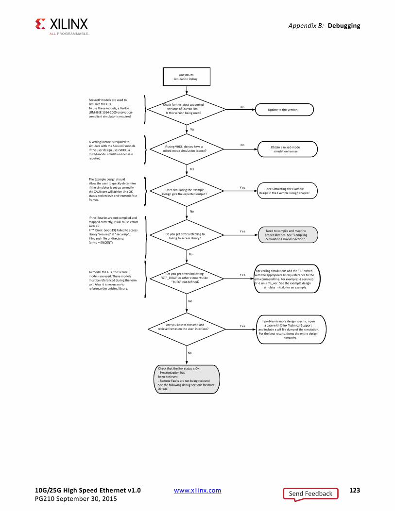
10G/25G High Speed Ethernet v1.0 www.xilinx.com 123PG210 September 30, 2015
Appendix B: Debugging
X-Ref Target - Figure B-1
Send Feedback
10G/25G High Speed Ethernet v1.0 www.xilinx.com 124PG210 September 30, 2015
Appendix B: Debugging
Hardware DebugHardware issues can range from link bring-up to problems seen after hours of testing. This section provides debug steps for common issues. The ChipScope debugging tool is a valuable resource to use in hardware debug. The signal names mentioned in the following individual sections can be probed using the ChipScope debugging tool for debugging the specif ic problems.
Many of these common issues can also be applied to debugging design simulations. Details are provided on:
• General Checks
• Ethernet Specific Checks
General Checks
Ensure that all the timing constraints for the core were properly incorporated from the example design and that all constraints were met during implementation.
• Does it work in post-place and route timing simulation? If problems are seen in hardware but not in timing simulation, this could indicate a PCB issue. Ensure that all clock sources are active and clean.
• If using MMCMs in the design, ensure that all MMCMs have obtained lock by monitoring the LOCKED port.
• If your outputs go to 0, check your licensing.
Timing
Ensure that timing is met according to the Vivado tools before attempting to implement the IP in hardware.
Transceiver Specific Checks
• Ensure that the polarities of the txn/txp and rxn/rxp lines are not reversed. If they are, these can be fixed by using the TXPOLARITY and RXPOLARITY ports of the transceiver.
• Check that the transceiver is not being held in reset or still being initialized. The
RESETDONE outputs from the transceiver indicate when the transceiver is ready.
• Place the transceiver into parallel or serial near-end loopback.
• If correct operation is seen in the transceiver serial loopback, but not when loopback is performed through an optical cable, it might indicate a faulty optical module.
Send Feedback
10G/25G High Speed Ethernet v1.0 www.xilinx.com 125PG210 September 30, 2015
Appendix B: Debugging
• If the core exhibits correct operation in the transceiver parallel loopback but not in serial loopback, this might indicate a transceiver issue.
• A mild form of bit error rate might be solved by adjusting the transmitter Pre-Emphasis and Differential Swing Control attributes of the transceiver.
Ethernet Specific Checks
A number of issues can commonly occur during the f irst hardware test of an Ethernet IP Core. These should be checked as indicated below.
It is assumed that the Ethernet IP Core has already passed all simulation testing which is being implemented in hardware. This is a pre-requisite for any kind of hardware debug.
The usual sequence of debugging is to proceed in the following sequence:
1. Clean up signal integrity.
2. Ensure that the SerDes achieves CDR lock.
3. Check that the 10/25G IP has achieved word sync.
4. Proceed to Interface and Protocol debug.
Signal Integrity
When bringing up a board for the first time and the 10/25G Ethernet IP Core does not seem to be achieving word sync, the most likely problem is related to signal integrity. Signal integrity issues must be addressed before any other debugging can take place.
Signal integrity should be debugged independently from the Ethernet IP Core. The following procedures should be carried out. (Note that it assumed that the PCB itself has been designed and manufactured in accordance with the required trace impedances and trace lengths, including the requirements for skew set out in the IEEE 802.3 specif ication.)
• Transceiver Settings
• Checking For Noise
• Bit Error Rate Testing
If assistance is required for transceiver and signal integrity debugging, contact Xilinx technical support.
N/P Swapping
If the positive and negative signals of a differential pair are swapped, then data cannot be correctly received on that lane. You should verify that the link has the correct polarity of each differential pair.
Send Feedback
10G/25G High Speed Ethernet v1.0 www.xilinx.com 126PG210 September 30, 2015
Appendix B: Debugging
Clocking and Resets
Refer to the Clocking and Resets in Chapter 3 for these requirements.
Ensure that the clock frequencies for both the High Speed Ethernet IP core as well as the Xilinx Transceiver reference clock match the configuration requested when the IP core was ordered. The core clock has a minimum frequency associated with it. The maximum core clock frequency is determined by timing constraints. The minimum core clock frequency is derived from the required Ethernet bandwidth plus the margin reserved for clock tolerance, wander and jitter.
The f irst thing to verify during debugging is to ensure that resets remain asserted until the clock is stable. It must be frequency-stable as well as free from glitches before the High Speed Ethernet IP Core is taken out of reset. This applies to both the SerDes clock as well as the IP Core clock.
If any subsequent instability is detected in a clock, the Ethernet IP core must be reset. One example of such instability is a loss of CDR lock. The user logic should determine all external conditions which would require a reset (e.g. clock glitches, loss of CDR lock, power supply glitches, etc.).
Configuration changes cannot be made unless the IP core is reset. An example of a configuration change would be setting a different maximum packet length. Check the description for the particular signal on the port list to determine if this requirement applies to the parameter that is being changed.
Interface Debug
LBUS Interface
The High Speed Ethernet IP core user interface is called the local bus (LBUS).
TX Debug
TX debug is assisted by diagnostic signals listed below:
Buffer Errors
Data must be written to the TX LBUS such that there are no overflow or underflow conditions.
When writing data to the LBUS, the tx_rdyout signal must always be observed. This signal indicates whether the TX buffer is within an acceptable range or not. If this signal is ever de-asserted, then you must stop writing to the TX LBUS immediately until the signal is
Send Feedback

10G/25G High Speed Ethernet v1.0 www.xilinx.com 127PG210 September 30, 2015
Appendix B: Debugging
asserted. The level at which tx_rdyout becomes de-asserted is determined by a pre-determined threshold.
If your configuration has been configured with a TX FIFO then you have two cycles to stop writing to the LBUS after tx_rdyout was de-asserted.
In the event that tx_rdyout is ignored, the signal tx_ovfout may be asserted, indicating a buffer overflow. This must not be allowed to occur. It is recommended that the High Speed Ethernet IP Core be reset if tx_ovfout is ever asserted. Do not attempt to continue debugging once tx_ovfout has been asserted until the cause of the overflow has been addressed.
When a packet data transaction has begun in the TX direction, it must continue until completion or there may be a buffer underflow as indicated by the signal stat_tx_underflow_err. This must not be allowed to occur; data must be written on the TX LBUS without interruption. Ethernet packets must be present on the line from start to end with no gaps or idles. If stat_tx_underflow_err is ever asserted, debugging must stop until the condition which caused the underflow has been addressed.
RX Debug
Consult the port list section for a description of the diagnostic signals which are available to debug the RX.
stat_rx_block_lock
This signal indicates that the receiver has detected and locked to the word boundaries as defined by a 01 or 10 control or data header. This is the first step to ensure that the 10/25G Ethernet IP is functioning normally.
CAUTION! Under some conditions of no signal input, the SerDes receiver exhibits a steady pattern of alternating 1010101.... This may cause erroneous block lock, but still indicates that the receiver has detected the pattern.
stat_rx_bad_fcs
A bad FCS indicates a bit error in the received packet. An FCS error could be due to any number of causes of packet corruption such as noise on the line.
stat_rx_local_fault
A local fault indication may be locally generated or received. Some causes of a local fault are:
• block lock not complete
• high bit error rate
Send Feedback
10G/25G High Speed Ethernet v1.0 www.xilinx.com 128PG210 September 30, 2015
Appendix B: Debugging
• overflow or underflow
Loopback Check
If the Ethernet packets are being transmitted properly according to 802.3, there should not be RX errors. However, the signal integrity of the received signals must be verif ied f irst.
To aid in debug, a local loopback may be performed with the signal ctl_local_loopback. This connects the TX SerDes to the RX SerDes, effectively bypassing potential signal integrity problems. The transceiver is placed into "PMA loopback", which is fully described in the transceiver product guide. In this way, the received data can be checked against the transmitted packets to verify that the logic is operating properly.
Protocol DebugTo achieve error-free data transfers with the Ethernet IP core, the 802.3 specif ication should be followed. Note that signal integrity should always be ensured before proceeding to the protocol debug.
Diagnostic Signals
There are many error indicators available to check for protocol violations. Carefully read the description of each one to see if it is useful for a particular debugging problem.
The following is a suggested debug sequence:
1. Ensure that Word sync has been achieved.
2. Make sure there are no descrambler state errors.
3. Eliminate CRC32 errors, if any.
4. Make sure the LBUS protocol is being followed correctly.
5. Ensure that there are no overflow or underflow conditions when packets are sent.
Statistics Counters
After error-free communication has been achieved, the statistics indicators can be monitored to ensure that traff ic characteristics meet expectations. Note that some signals are strobes only, which means that the counters are not part of the IP core. This is done so that the counter size may be customized. Counters are optionally available with the AXI interface.
Send Feedback
10G/25G High Speed Ethernet v1.0 www.xilinx.com 129PG210 September 30, 2015
Appendix C
Additional Resources and Legal Notices
Xilinx ResourcesFor support resources such as Answers, Documentation, Downloads, and Forums, see Xilinx Support.
ReferencesThese documents provide supplemental material useful with this product guide:
1. 25G and 50G Ethernet Consortium Schedule 3 version 1.4 (August 28, 2014) (http://25gethernet.org/)
2. IEEE Standard 802.3-2012 (standards.ieee.org/findstds/standard/802.3-2012.html)
3. IEEE P802.3by/D01 (ieee802.org/3/by/)
4. Vivado® Design Suite User Guide: Designing IP Subsystems using IP Integrator (UG994)
5. Vivado Design Suite User Guide: Designing with IP (UG896)
6. Vivado Design Suite User Guide: Getting Started (UG910)
7. Vivado Design Suite User Guide: Logic Simulation (UG900)
8. Vivado Design Suite User Guide: Programming and Debugging (UG908)
9. Vivado Design Suite User Guide - Implementation (UG904)
10. Vivado Design Suite AXI Reference Guide (UG1037)
11. LogiCORE IP Xilinx High Speed Ethernet Product Guide (PG183)
Send Feedback

10G/25G High Speed Ethernet v1.0 www.xilinx.com 130PG210 September 30, 2015
Appendix C: Additional Resources and Legal Notices
Revision HistoryThe following table shows the revision history for this document.
Please Read: Important Legal NoticesThe information disclosed to you hereunder (the “Materials”) is provided solely for the selection and use of Xilinx products. To the maximum extent permitted by applicable law: (1) Materials are made available “AS IS” and with all faults, Xilinx hereby DISCLAIMS ALL WARRANTIES AND CONDITIONS, EXPRESS, IMPLIED, OR STATUTORY, INCLUDING BUT NOT LIMITED TO WARRANTIES OF MERCHANTABILITY, NON-INFRINGEMENT, OR FITNESS FOR ANY PARTICULAR PURPOSE; and (2) Xilinx shall not be liable (whether in contract or tort, including negligence, or under any other theory of liability) for any loss or damage of any kind or nature related to, arising under, or in connection with, the Materials (including your use of the Materials), including for any direct, indirect, special, incidental, or consequential loss or damage (including loss of data, profits, goodwill, or any type of loss or damage suffered as a result of any action brought by a third party) even if such damage or loss was reasonably foreseeable or Xilinx had been advised of the possibility of the same. Xilinx assumes no obligation to correct any errors contained in the Materials or to notify you of updates to the Materials or to product specifications. You may not reproduce, modify, distribute, or publicly display the Materials without prior written consent. Certain products are subject to the terms and conditions of Xilinx’s limited warranty, please refer to Xilinx’s Terms of Sale which can be viewed at http://www.xilinx.com/legal.htm#tos; IP cores may be subject to warranty and support terms contained in a license issued to you by Xilinx. Xilinx products are not designed or intended to be fail-safe or for use in any application requiring fail-safe performance; you assume sole risk and liability for use of Xilinx products in such critical applications, please refer to Xilinx’s Terms of Sale which can be viewed at http://www.xilinx.com/legal.htm#tos.© Copyright 2015 Xilinx, Inc. Xilinx, the Xilinx logo, Artix, ISE, Kintex, Spartan, Virtex, Vivado, Zynq, and other designated brands included herein are trademarks of Xilinx in the United States and other countries. All other trademarks are the property of their respective owners.
Date Version Revision
09/30/2015 1.0 Initial Xilinx release.
Send Feedback