104 ieee transactions on education, vol. …rhabash/smpsmatlab.pdf · 104 ieee transactions on...
TRANSCRIPT

104 IEEE TRANSACTIONS ON EDUCATION, VOL. 54, NO. 1, FEBRUARY 2011
A Switching-Mode Power Supply Design Tool toImprove Learning in a Power Electronics Course
Pablo F. Miaja, Student Member, IEEE, Diego G. Lamar, Member, IEEE,Manuel Arias Pérez de Azpeitia, Student Member, IEEE, Alberto Rodríguez, Student Member, IEEE,
Miguel Rodríguez, Student Member, IEEE, and Marta M. Hernando, Member, IEEE
Abstract—The static design of ac/dc and dc/dc switching-modepower supplies (SMPS) relies on a simple but repetitive process. Al-though specific spreadsheets, available in various computer-aideddesign (CAD) programs, are widely used, they are difficult to use ineducational applications. In this paper, a graphic tool programmedin MATLAB is presented, which allows students to apply and toreflect upon the knowledge acquired in theoretical classes. Thistool has been successfully employed in the course “Sistemas Elec-trónicos de Alimentación” in the Telecommunications Engineeringdegree as part of a project in new education methods (Universityof Oviedo project PB-08–019). During practical sessions, the stu-dents used the tool to design a SMPS, achieving better learningresults than was the case without the tool. In addition, the tool wassuccessfully used to improve the students’ theoretical knowledge ofthe subject.
Index Terms—Computer-aided engineering, education, edu-cational technology, learning, project-based learning, switchingpower supplies teaching.
I. INTRODUCTION
T ELECOMMUNICATIONS engineering is a five-year de-gree program in the University of Oviedo (Gijón, Spain).
The courses that make up this degree cover topics that rangefrom the mathematical background of telecommunications toelectronic design with special emphasis given to radio andto high-frequency designs. Computer networks and computerscience also feature prominently. During their last year, thestudents have to choose between various elective courses inorder to specialize. The course ”Sistemas Electrónicos deAlimentación” (”Electronic Power Systems”) [1] is one ofthese elective courses offered. Its main topics are the typicaltopologies of ac/dc and dc/dc switching-mode power supplies(SMPS), magnetic design, and power devices. Only these typesof conversions are covered in this power electronics coursebecause they are the most common in telecommunicationequipment.
Manuscript received May 21, 2009; revised November 17, 2009; acceptedMarch 11, 2010. Date of publication April 15, 2010; date of current versionFebruary 02, 2011. This work was supported by the University of Oviedo underthe project in new educational methods: PB-08–019.
The authors are with the Power Supply Systems Group, Department ofElectrical and Electronic Engineering, University of Oviedo, Gijón 33204,Spain (e-mail: [email protected]; [email protected];[email protected]; [email protected]; [email protected]; [email protected]).
Color versions of one or more of the figures in this paper are available onlineat http://ieeexplore.ieee.org.
Digital Object Identifier 10.1109/TE.2010.2046490
From their courses, students can learn a great deal of telecom-munications theory, but they are rarely offered the opportunityto work on the development of a real product, either softwareor hardware. However, the ability to apply their knowledge ina real situation is one of the most necessary skills that an engi-neer must have. A training in the development of a real productgives the students the opportunity to face some of the real prob-lems they will encounter in their future careers. One of the betterways to learn something is by the methodology often known aslearning by doing: To learn something properly, you must actu-ally do it yourself. That is the reason why the teachers giving thecourse offer the students the opportunity to build a full SMPSso they can apply the knowledge acquired in theoretical classes.
In order to accomplish these objectives, a lot of preliminarywork has to be done: Students should learn all the theory behindthe development of ac/dc and dc/dc power converters beforeworking on a real one. This is explained in theoretical classesthat cover all the aspects involved in the design: the specifica-tions of the semiconductor devices, the design of magnetic com-ponents, the static and dynamic models of the converters, and soon. The students have to pass an exam on those theoretical con-cepts and must demonstrate that they have understood all theconcepts taught by developing a simple spreadsheet to analyzea converter not covered in class. This spreadsheet is often donein MATLAB. The last, but not the least significant, part of thecourse is the design and construction of the power supply, wherethey have to apply all the theoretical concepts they have learned.This paper is focused on this point: the proper design and con-struction of an SMPS during the practical sessions of a course.
One of the main problems of making real power suppliesin power electronics courses is the time that must be spent onthe laborious calculations needed. These are based on staticmodels of power supply topologies, widely known and refer-enced in [2]–[5]. These models are fundamental for correctlycomprehending how switching power supplies work, and theyare explained in the theoretical classes of power electroniccourses. However, these models imply numerous calculationsthat take a lot of time. This makes it very difficult to completea power supply design during the theoretical sessions of thecourse. Thus, design time must be optimized. This could beachieved by using computer programs. Traditionally, designershave written specific spreadsheets for every task needed inthe design process. Some of these are used for the static de-sign, others for the estimation of efficiency, and others for themagnetic components needed. These spreadsheets were notdesigned for educational purposes and are lacking in usability,so a lot of time is spent getting used to the tool. This work
0018-9359/$26.00 © 2010 IEEE
MIAJA et al.: SWITCHING-MODE POWER SUPPLY DESIGN TOOL 105
methodology cannot be used for educational purposes becauseof this long learning curve.
This four-month, one-semester course, as well as covering alarge amount of theory, has seven 2-h practical sessions. Thoseteaching the course are experts in the design of SMPS who knowthat it is impossible to design a full power supply during theseven practical sessions. Therefore, the design somehow needsto be sped up so that the students will have enough time tothink about the way the theoretical concepts are connected tothe development of the practical sessions. An appropriate wayto achieve this is presented here.
This paper presents a MATLAB tool for static analysis ofSMPS. It is specifically designed to be easy to work with sothat students can start the static design process without diffi-culty. Once the architecture is chosen, the student has to fill outa form with the static specifications of the power supply. Theprogram will make all the necessary calculations and shows theresults as a set of graphics and text windows. Another featureof the tool is that it allows a user to estimate losses in the realsemiconductor devices in order to show students a realistic viewof the work of a designer. It also provides help in taking deci-sions in the tradeoff between cost and efficiency. Moreover, thegraphic results can help lecturers in their explanations of con-verter models, showing where the boundary between continuousconduction mode (CCM) and discontinuous conduction mode(DCM) lies and the evolution of the currents and voltages in theconverter in relation to the power processed. In addition to theuse of this tool to complete the design process, a similar toolis also included to help in the design of the magnetic elements,such as inductors and transformers.
Before the development of this tool, students were expectedto build the same SMPS, but both the static design and the de-sign of the magnetic elements were carried out by the teacher. Ifthe students wanted to, they could check the design at home, andthey were encouraged to do so. However, because of the labo-rious calculations involved, very few students actually checkedthe design themselves, therefore very few could link what theyhad learned in theoretical classes with the practical sessions. Theidea was to provide a tool that helps to make that connection byavoiding lengthy calculations. Hence, the students have moretime in practical sessions to reflect on how to apply their ac-quired knowledge. In the current version of the course, everystudent is obliged to carry out the design of the SMPS during thefirst practical session so that they all have a better understandingof the decisions taken in the design process. Other course objec-tives, like the acquisition of power electronics concepts and thestatic and dynamic analysis of ac/dc and dc/dc power supplies,are evaluated by an exam and the development of an originalspreadsheet of a converter topology not covered in class.
MATLAB was chosen because students are used to workingwith it in previous courses. In other telecommunications degreesubjects such as Digital Signal Processing, MATLAB is a defacto standard, and there are some educational tools available[6], [7]. Students know its programming language, so they canunderstand how the tool is made, manage their results in a dif-ferent way, or improve the tool with other converter topologies(for example, the spreadsheet developed as another project inthe course). There are also more tools for power electronics de-
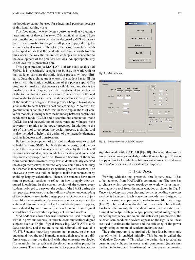
Fig. 1. Main window.
Fig. 2. Boost converter with PFC module.
sign that work with MATLAB [8]–[10]. However, they are in-tended for acquiring knowledge rather than applying it. There isa copy of this tool available at http://www.unioviedo.es/ate/sea/archivos/converters.zip for evaluation purposes.
II. BASIC USAGE
Working with the tool presented here is very easy. It hasto be launched from MATLAB’s command line. The user hasto choose which converter topology to work with or launchthe magnetics tool from the main window, as shown in Fig. 1.Once a topology has been chosen, the corresponding convertermodule is launched. Each converter module was designed tomaintain a similar appearance in order to simplify their usage(Fig. 2). The window is divided into two parts. The left sidehas to be filled in with the specifications of the converter, suchas input and output voltage, output power, output voltage ripple,switching frequency, and so on. The datasheet parameters of theselected semiconductor devices appear on the right side; theseare used to estimate the losses and the efficiency of the powersupply using commercial semiconductor devices.
The entire program is controlled with just four buttons, onlyone of which is enabled initially. This button is called the”Calculate Converter.” This takes the design data to calculatecurrents and voltages in every main component (transistors,diodes, inductor, and transformer) of the power converter.

106 IEEE TRANSACTIONS ON EDUCATION, VOL. 54, NO. 1, FEBRUARY 2011
Fig. 3. Magnetics module screenshot.
When the calculations are finished, the results are shown invarious graphics and text windows. Now, the button called”Efficiency Test” is enabled. With the previously calculatedvoltages and currents, the losses in the semiconductor devicesare estimated using the datasheet parameters that were enteredon the right side of the window. Graphic and text windowsshowing the efficiency under various conditions are shown. Thenext buttons are used to show all the previously calculated dataand to export these to MATLAB’s workspace.
Data are exported to MATLAB as a structure, where all theinformation shown and some other results are stored. Thesedata include currents and voltages in every main component andswitching and conduction losses. With this structure, a deeperanalysis can be developed, using MATLAB’s facilities. Thiskind of analysis can be programmed by students because of theirprior knowledge of MATLAB’s programming language.
Working with this tool mimics the manual design processfor a SMPS power supply. First, the static calculations are car-ried out, in which all the currents and voltages are calculated.Then, using these results, components are selected to choosewhich semiconductor devices handle these currents and volt-ages. Thus, the designer also evaluates the losses on the semi-conductor devices.
The Magnetic Elements Module is used after the Convertermodules. When the currents and voltages on the magnetic el-ement have been calculated for the chosen topology, the Mag-netic Element Module can be launched from the main window(Fig. 1). There is a list of components that can be chosen for thedesign (inductor, transformer, coupled inductor). Only the fieldsnecessary to complete the design are enabled for students to fillin with the data provided by the converter module. As shown inFig. 3, the right side of the window shows a list with differentmaterials and magnetic cores. A small database with E and ETDcores and 3F3 materials is provided. Students can complete thisdatabase with more cores and materials. The tool offers informa-tion about the number of turns, diameter of the wire, and numberof wires in parallel to achieve the desired component. An esti-mation of the temperature reached by the magnetic element isalso shown in order to help students to decide on the size andshape of the core.
The following section shows the theoretical background andan example of a CA/CC converter usually used in power supply
architecture: a boost converter with power factor correction(PFC). This is a typical converter in PFC topologies. Studentswill have made one of these during the course’s practicalsessions.
III. THEORETICAL BACKGROUND
The static design of a SMPS power supply is a well-knownsubject fully treated in the literature. The main references usedfor the development of this work, and given to the students intheir lecture notes, are [2]–[5]. Following the specific set ofequations for each converter topology, the program calculatescurrents and voltages in each component. With all this informa-tion, the losses, and then the efficiency, can be calculated. Theseequations, like those that set the boundary limits between CCMand DCM, those that link the duty cycle with the voltage rela-tionship between the input and the output, and the input speci-fications, are explained in theoretical classes; however, they arebeyond the scope of this paper.
From the current through every component, the conductionlosses in the semiconductor devices are estimated by assumingclassical models: A MOSFET on ON state behaves as a resistor,and a forward-biased diode behaves as a resistor connected inseries to an ideal voltage source. The values of these param-eters are found on the datasheets of semiconductor manufac-turers and entered into the program by the students. Equation(1) shows the estimation of conduction losses in a MOSFET,where is the effective current through the transistorand the ON state resistor. Equation (2) is used to calculatethe conduction losses in a diode, is the effective current,
is the mean value of the current through the diode, isthe forward voltage drop, and is its resistance.
(1)
(2)
To calculate the switching losses, the classical piecewiselinear model is used [11]. This model takes into account thedifferent parasitic capacitances that are present in both thetransistor and the diode. In this case, the MOSFET and diodeparameters are found on the datasheets of semiconductormanufacturers, too. These loss models are used because, whilethey are simple and easy to understand, they are usually usedas a first approach to estimate semiconductor losses in a realdesign. The design of a magnetic element is usually basedon finding the number of turns that minimizes losses whileavoiding saturation of the core [13]–[15]. This tool is based onthat principle.
Losses in the copper are calculated by estimating the resis-tance of the windings and the effective current through them,which are calculated in the converter modules. Resistance is es-timated by the expression (3) that relates the resistance to theresistivity of the material, , the mean length of a turn on thewinding, , which is given by the core vendors, the numberof turns , and the section of the wire . The section ofthe wire is calculated by assuming that all the window area ofthe coil former will be filled with copper. As it is impossible toachieve that with a wire, an approximation is used by using a

MIAJA et al.: SWITCHING-MODE POWER SUPPLY DESIGN TOOL 107
smaller window area, usually 30% of the data given by the coilformer vendor.
(3)
The process to estimate the losses in the magnetic core is alittle bit more complicated. While estimating the losses in thewinding is quite straightforward, losses in the magnetic corerequire a more complex approach. Magnetic material vendorsoften offer some curves relating the peak magnetic flux densitywith the power loss density [12], so the losses can be estimatedby multiplying the effective volume of the core by the powerloss density obtained from the curves. These curves were pa-rameterized and programmed in the application. Equation (4)shows the parameterization used, where is the peak mag-netic flux density, is the frequency, and , , and are con-stants depending on the material chosen. Peak magnetic flux iscalculated using the expression in (5), which relates the valueof the inductance , the peak ac component of the current ,the number of turns , and the effective section of the core ,with it.
(4)
(5)
The losses are a function of the number of turns, thereforethe optimal number has to be chosen. The process is to setas the number of turns that minimizes the overall losses, as canbe seen in Fig. 12 where the losses on an inductor are depicted.However, saturation of the core must be avoided. This is checkedby comparing the expression in 6 , where is the maximumcurrent through the winding, the number of turns, is theequivalent area of the core, and is the value of the inductance,with the maximum magnetic flux supported by the core, shownin the datasheet of the material.
(6)
Due to the switching frequency used in the SMPS studied inthe course, the skin effect has to be taken into account. Theskin effect describes the way in which current flows throughthe outer part of a wire. With increasing frequency, the currenttends to flow through a smaller area, and then the resistanceand the losses increase. The tool calculates the skin depth andoffers advice about the optimum wire diameter and the numberof wires in parallel to configure a litz wire that can handle all thecurrent that has to flow while avoiding the skin effect.
These are the kinds of facts that the students learn in the the-oretical classes. What this tool offers is a way to make the cal-culations faster and then improve the practical sessions, wherethe students can apply all the knowledge they have gathered intheoretical classes.
IV. EXAMPLE OF A BOOST CONVERTER WITH PFC
As an example, a boost converter with power factor correctionwas designed using this tool. Students made a low-power SMPS
Fig. 4. Results on boost PFC converter.
power supply in the practical sessions for reasons of safety. Theboost converter specifications are the following:
• Minimum Input Voltage: 80 V RMS;• Maximum Input Voltage: 265 V RMS;• Nominal Input Voltage: 230 V RMS;• Output Voltage: 400 V;• Output Voltage Ripple: 1%;• Output Power: 1000 W;• Switching Frequency: 100 kHz;• Grid Frequency: 50 Hz.All of these specifications are entered in the fields on the left
side of the module window, as seen in Fig. 2. There are severalways to calculate the inductor; one of the most common is to fixthe limit between CCM and DCM. Here, it is fixed to half thepower handled, 500 W. A window showing the results of thestatic design (Fig. 4) appears as soon as the first button, “Cal-culate Converter,” is clicked. Some useful data for choosing thesemiconductor devices, such as maximum voltages and max-imum effective current on both the transistor and the diode, areshown. The inductor and capacitor values and the maximum andminimum duty cycle are also provided.
Currents through the most important elements—namely theinductor, transistor (Fig. 5), and diode (Fig. 6)—are plottedagainst the conduction angle , where is the linearangular frequency of the mains. With this information, it ispossible to find devices that can meet the specifications andthen evaluate the resulting efficiency. The MOSFET tran-sistor SPW47N60C3 and the UltraFast diode STTA2006Pwere chosen as an example. Real specifications, taken fromdatasheets [16], [17], were entered on the right side of thewindow (Fig. 2).
There are also fields to enter the driver current and voltageand the number of transistors and diodes in parallel. Putting de-vices in parallel is a usual arrangement to reduce current stressesand conduction losses, so it has to be taken into account forthe estimation of the losses. Semiconductor losses are dividedinto switching losses and conduction losses (these data are notshown, but are stored in the exported structure). As seen inFig. 7, the efficiency at the maximum, minimum, and nominalinput voltages is shown by pushing the “Efficiency Test Button.”This level of detail helps students to see actual problems inpower supply design, such as the tradeoff between efficiencyand the number of devices in parallel. Fig. 8 explains this con-cept by plotting efficiency versus the number of devices in par-allel, which is directly related to cost.

108 IEEE TRANSACTIONS ON EDUCATION, VOL. 54, NO. 1, FEBRUARY 2011
Fig. 5. Currents through the transistor in the designed boost converter.
Fig. 6. Currents through the diode in the designed boost converter.
Fig. 7. Efficiency of the boost converter.
V. EXAMPLE OF AN INDUCTOR
As an example of how the Magnetic Module works, the in-ductor needed by the previously described boost converter willbe explained.
Once the magnetic module has been launched, the user mustchoose what type of magnetic element to design. In this case,
Fig. 8. Efficiency of the boost converter versus the number of devices in par-allel.
Fig. 9. Magnetics module screenshot with data for the inductor.
the inductor was chosen, and the application activates the fieldsthat need to be filled in to design the component, as can be seenin Fig. 9.
These data must be taken from the information given by theresults from the chosen converter design module. This was aboost converter in the previous example. The value of the in-ductor was taken from the text window that shows the converterparameters (Fig. 4), while the various values for currents weretaken from the graphics that show the boost converter’s inductorcurrents (Fig. 10). Once the fields have been filled in with thesedata, the material and shape of the core must be chosen. Cur-rently, only two materials and a variety of E- and ETD- shapedcores are offered, but this database can be enhanced with morecores and materials. This database stores the data needed to cal-culate the magnetic behavior of the core, information that is of-fered by magnetic material vendors in their datasheets.
After all the fields have been filled in, the user must clickthe ”Calculate” button. The program brings up a text window(Fig. 11) with the number of turns, the size of the gap, an esti-mation of the temperature reached by the inductor, the diameter

MIAJA et al.: SWITCHING-MODE POWER SUPPLY DESIGN TOOL 109
Fig. 10. Currents through the inductor in the designed boost converter.
Fig. 11. Data for making the inductor.
of the wire to avoid the skin effect, and the number of wires inparallel needed to carry the desired amount of current.
A picture (Fig. 12) showing the evolution of the losses alongthe number of turns is also shown. This picture shows the differ-ence between the losses in the copper, due to the resistance ofthe winding, and the losses in the core, due to the current ripple.
Figs. 11 and 12 provide a visual feedback for their design. Ascan be seen, several magnetic designs can be made for the samespecifications. Students have to assemble the best option.
Using this tool, the lengthy process required to design of amagnetic element is shortened by the use of the computer. Thecalculations involved in the manual process are not too difficult,but there are a lot of small details concerning the parameteriza-tion of the behavior of magnetic materials and the shape of thecore that are critical. Making a mistake in these details is almosttotally avoided by all of these data being taken from the data-base.
VI. EDUCATIONAL BENEFITS
It is important to note that the tool is not designed to teachpower electronics concepts. Students should acquire theirknowledge in theoretical classes, and this should be evaluatedby the exam and the theoretical project (the spreadsheet theyare required to make). The purpose of this tool is to enhancethe application of the knowledge acquired in theoretical classes
Fig. 12. Losses in a magnetic component.
during the practical sessions, where students design and build aSMPS. The objective of the use of this tool in practical sessionsis to create a connection between theoretical concepts of powerelectronics and their practical application. This new situationfacilitates the correct comprehension of the knowledge acquiredand significantly enhances learning.
The main educational characteristics of the tool presentedhere are that it does the following.
• Shortens the time needed to design and build a SMPSin practical sessions. Therefore students have more timeavalaible to relate theoretical concepts to the practicalproblems presented in design sessions.
• Shows the results of the static study in a user-friendly way.This improves the assimilation of theoretical concepts be-cause this tool can be used to evaluate the evolution of thepower supply behavior while changing design parameters.
• Allows students to see the process they will follow in thepractical sessions. The way they use the tool resembles thedesign process usually followed by SMPS designers as afirst approach.
Before this tool was available in the practical sessions of thecourse “Sistemas Electrónicos de Alimentación,” students stillhad to make the same SMPS power supply. As the lecturersinvolved realized that the available time was not sufficient forstudents to complete the entire design process, they themselvescarried out both the static design and the magnetic elements de-sign. Students were expected to check this design at home, butvery few of them did so. In fact, during the practical sessions,the students only assembled the converter, but they did not re-alize why the specific component values were chosen. Only thebetter students who were willing to spend time at home checkingthe design really understood the whole process. In order to solvethis problem, the lecturers introduced this tool, which allows thestatic design to be carried out by the students in their practicalsessions. This means that all the students know why each com-ponent was chosen and therefore develop a better understanding

110 IEEE TRANSACTIONS ON EDUCATION, VOL. 54, NO. 1, FEBRUARY 2011
Fig. 13. Efficiency of a half-bridge converter.
of the overall design of a SMPS power supply by applying theirpower electronics knowledge.
Next, a few features that a good student can use to improvetheir knowledge will be introduced.
• By varying the power ratio at which the power supplychanges from CCM to DCM, the student will see how thisaffects the efficiency, as well as how this new value of in-ductance affects the physical values of the magnetic ele-ment that is needed.
• A similar study can be performed by varying the switchingfrequency. While increasing the switching frequency, thevalues of the inductor and the capacitor needed to meetthe voltage ripple requirement decrease, but the switchinglosses increase.
• As the tool allows the real semiconductor parameters to bevaried, the student can see how a better transistor or diodeimproves the efficiency of the power supply.
• Other important facts shown are the efficiency representedversus the number of semiconductor devices in parallel, asin Fig. 13, which is a representation of efficiency versuscost. This can help the students to make decisions aboutsome of the various tradeoffs in this application, which isone of the most important skills for an engineer.
• By referring to Fig. 13, a lecturer can easily explain theevolution of efficiency versus the power processed. As canbe seen at low power, every loss represents an important de-crease in efficiency. As the power increases, the efficiencywill increase until the power is so large that the currentsinvolved imply major conduction losses.
• While the tool is designed for the static design of the con-verter, students can export the data to MATLAB and thenbuild the dynamic model with the actual values of the com-ponents. Using the tools provided with MATLAB and thedata from the application, students can display Bode dia-grams and design the control for its power supply. Anotheruseful improvement of the tool will be its integration with
a control design tool, for either analog or digital control.An example of the capabilities of MATLAB to deal withcontrol and power electronics can be seen in [18], whereMATLAB is combined with SPICE simulations to developa system identification program.
• Using this tool, the magnetic design time is improved, andgraphics like the one on Fig. 11 are shown. These graphicsare very similar to the ones shown in the lecture notes,but with this tool, students can see how they vary withthe different cores used and can better understand how thesize and shape of the core is involved in the design. As themagnetic elements are usually handmade, the less time thestudents employ in their design, the more time they willemploy in the construction of the component, which is amanual skill that has to be learned in the practical class.This construction process involves various details, such asthe way of carrying out the winding and how to make thelitz wire, which take a lot of time for a class with manystudents. In fact, the magnetic design session became moreintuitive and practical.
Nevertheless, it is important to keep in mind, as the studentsappreciate, that the tool works with simplified but accuratemodels. These models will not reflect all the effects involved inthe actual behavior of SMPS, although they are widely used indesigning SMPS as a first approach.
A much more detailed process can be followed by the useof simulation tools as pSPICE [19]. The waveforms acquiredwill be much more accurate. However, working with a simu-lation program is quite difficult and requires a lot of trainingin using the program. One of the worst drawbacks of simula-tion programs is the dependence on the vendor’s models for thesemiconductor devices. The use of idealized models can help,but this brings a lack of accuracy similar to that seen from theuse of simplified models. In this case, the idea was to motivatethe students with a real project. In fact, students prefer to handlereal devices rather than a simulation tool in a computer, as theydo in so many courses. Other possibilities are to include sim-ulations on the development of the prototype, but this was notpossible due to the limited time available. Nevertheless, whileit is impossible to neglect the power of circuit simulation pro-grams, for the reasons stated, the use of these simulation pro-grams is recommended only for long-lasting projects such asMaster’s theses, not for intensive use in practical courses suchas that taught by the authors.
Another approach is the use of computer-aided learning pro-grams, such as those described in [20]. These are designed toteach the fundamentals of power electronics, as taught in theo-retical classes. A good compromise between the theoretical andpractical approach is the tool described in [21], which helps inthe design while showing the waveforms on the different ele-ments. However, although this is good for teaching purposes, itis not focused on the design of a SMPS, which is the goal of thepractical sessions.
VII. RESULTS
To evaluate the actual success achieved by the use of this tool,the authors analyzed the results achieved by the students. The

MIAJA et al.: SWITCHING-MODE POWER SUPPLY DESIGN TOOL 111
Fig. 14. Marks obtained in the subject versus time.
Fig. 15. (a) Percentage of students who finished the converter in practical ses-sions. (b) Hours used in training for the practical sessions.
evaluation method of the course ”Sistemas Electrónicos de Al-imentación” is fully described in [1] and has not changed sincethe course was first offered.
The students fail if they get less than 5 points, and the topmark is 10 points. These marks are grouped in four intervals,which represent the actual qualification that is delivered to thestudent. Fig. 14 shows the marks obtained by the students from2004–2009. As it can be seen in Fig. 14, although most of thestudents passed the subject, the percentage getting the highestmarks increased significantly with the introduction of the toolpresented in this paper.
The most common mark is between 7 and 8.5, which is quitehigh. In previous years, most students got a mark between 5 and7, with 5 being the lowest mark needed to pass the subject. Thus,there is a significant improvement in the students’ learning ofpower electronics because they assimilate theoretical conceptsand are able to apply them to the practical sessions. It can beinferred that exam marks and the results of the theoretical work(the spreadsheet they are required to create) increase becausea student must apply his or her knowledge in order to obtainsignificant learning.
Some other benefits are shown in Fig. 15. The greatest part ofstudent’s grade is obtained by their building a switching powersupply during the practical sessions of the course. Before the useof the tool, there were many students who could not completethis in the time available in the practical sessions [Fig. 15(a)].Those students needed to spend more hours in the laboratory,which was problematic for them. The other benefit is reflectedby Fig. 15(b), which represents the number of hours needed bythe students to prepare the practical sessions at home. With theaid of the tool presented in this paper, it has become closer to the20 h that the lecturers had planned, as the project on the SMPScannot interfere with work on other courses.
It can be argued that the students’ grades are not a good metricto evaluate their degree of learning. However, the main part ofa student’s grade is awarded for the way s/he has worked on
the SMPS power supply [1]. A good student who made his orher power supply work without any help and can explain tothe teacher every part of the design process will get the highestmark. As all the students are now able to accomplish the properdesign and building in the proposed practical sessions, theirmarks had increased, as reflected in Fig. 14.
The results of the use of the tool presented in this paper arealso reflected in the periodical surveys made by the University ofOviedo to assess the quality of their degrees. In those surveys,the students are asked to rate different aspects of the coursesand then give an overall score. This process is repeated withall the courses of the degree. In Fig. 16, the results of the course”Sistemas Electrónicos de Alimentación,” in which this tool hasbeen used, are shown with respect to the average results from allthe courses of the degree in Telecommunications Engineering.
Prior to the introduction of the tool presented in this paper, thecourse was rated similarly to other courses. Since its first use in2008, the course has obtained higher marks for all the pointsevaluated. Fig. 16 shows the results of some of points evaluatedin the survey, such as the way in which the practical sessions areplanned [Fig. 16(a)], how students evaluate the didactical mate-rial given [Fig. 16(b)], and how they rate the new knowledgeacquired [Fig. 16(c)]. Such a good rating represents an affirma-tion for the lecturers involved. As a result of the survey, someconclusions can be drawn: An experience like building a SMPSis very motivating, which leads to a good evaluation. A signif-icant part of this positive evaluation is due to the fact that thepractical sessions were properly planned and had a good infra-structure.
VIII. CONCLUSION
A simple but accurate tool for educational purposes has beenpresented in this paper.
This tool has been successfully used in the course “SistemasElectrónicos de Alimentación” in the TelecommunicationsEngineering degree program at the University of Oviedo. Ithas helped students to design and build a power supply system(Fig. 17), saving a lot of time and enhancing their significantlearning. “Sistemas Electrónicos de Alimentación” is a coursetaught in the last year of the Telecommunications Engineeringdegree.
In the practical sessions of the course, students are requiredto build a complete boost converter. While the converter used tobe designed and tested by the lecturer, students now make onethemselves to benefit from the practical application of their the-oretical skills. There are seven practical sessions, each lasting2 h. Although these practical sessions are supposed to be suffi-cient to complete the design and construction of the converter,in the lecturers’ experience, it is very difficult to do so. There-fore, the use of a user-friendly CAD tool is highly desirable. Thetool presented in this paper met with great success in the staticdesign process; all the students made their converter work prop-erly and completed the entire design process. Students tested thecomponent selection with the aid of this tool. The static designis part of the firsts practical session, while the later sessions aretaken up with the design and building of the inductor, where thistool was also used, and the assembly of the power supply. Allthe students reported that the tool was very useful and showed an

112 IEEE TRANSACTIONS ON EDUCATION, VOL. 54, NO. 1, FEBRUARY 2011
Fig. 16. Results of the survey: (a) rating of the hours needed by the students to plan the practical sessions, (b) rating of the didactical materials used, and (c)overall rating of the subject.
Fig. 17. Prototype made in practical sessions.
in-depth knowledge of the design of SMPS power supplies. Thiscontrasts with the situation prior to the introduction of the tool,when the students did all the calculations by hand. Because ofthis lengthy process, the little reflection was shown in the qualityof the design of SMPS. Therefore, this tool raises the averagelevel of learning in the design of SMPS power supplies becauseit is focused creating a scenario where students are able to applythe theoretical concepts explained in lectures to designing andbuilding a SMPS.
Although this tool is not designed to teach students howpower supplies work, it does help the lecturer to explain somedifficult concepts by using the graphic results obtained duringthe design process. These explanations take place during thepractical sessions in which students have to build a full SMPS.Therefore, the objective is to connect theoretical with practicalconcepts to obtain significant learning by applying the acquiredknowledge.
Moreover, due to the fact that this tool is written in a pro-gramming language that students should already be acquaintedwith, they can understand how it works and improve it or use itin different applications. Another assignment used to evaluatestudents in the course is the design of a spreadsheet that ana-lyzes some aspects of a converter topology not studied in class.Students usually create this spreadsheet in MATLAB, thus fa-cilitating integration with the tool presented in this paper.
The benefits of using this tool are reflected in the marks ob-tained by the students (Fig. 14), the efficiency in the building ofthe prototype, and the student spending less hours while thereare more students who finish the SMPS power supply (Fig. 15).The results of the surveys made by the university also reflectthat the students valorize the subject better than the average ofthe subjects of the grade (Fig. 16). Therefore, the overall qualityof the student learning was improved by the use of this tool.
REFERENCES
[1] Web site of the subject Sistemas Electrónicos de Alimentación.[Online]. Available: http://directo.uniovi.es/Catalogo/FichaAsig-natura.asp?Asignatura=14003
[2] D. W. Hart, Introduction to Power Electronics. Englewood Cliffs, NJ:Prentice-Hall, 1997.
[3] M. H. Rashid, Power Electronics, Circuits, Devices and Applications,3rd ed. Upper Saddle River, NJ: Pearson, 2003.
[4] N. Mohan, T. M. Undeland, and W. P. Robbins, Power Electronics:Converters, Applications, and Design, 2nd ed. New York: Wiley,1995.
[5] R. W. Erickson and D. Maksimovic, Fundamentals of Power Elec-tronics, 2nd ed. Boston, MA: Kluwer, 2001.
[6] M. P. Fargues and D. W. Brown, “Hands-on exposure to signal pro-cessing concepts using the SPC toolbox,” IEEE Trans. Educ., vol. 39,no. 2, pp. 192–197, May 1996.
[7] M. Painter, “A software tool for introducing speech coding fundamen-tals in a DSP course,” IEEE Trans. Educ., vol. 39, no. 2, pp. 143–152,May 1996.
[8] F. Milano, “An open source power system analysis toolbox,” IEEETran. Power Syst., vol. 20, no. 3, pp. 1199–1206, Aug. 2005.
[9] J. F. Haffner, L. F. A. Pereira, and D. F. Coutinho, “Computer-assistedevaluation of undergraduate courses in frequency-domain techniquesfor system control,” IEEE Trans. Educ., vol. 49, no. 2, pp. 224–235,May 2006.
[10] E. Allen, N. LaWhite, Y. Yoon, J. Chapman, and M. Ilic, “Interac-tive object-oriented simulation of interconnected power systems usingsimulink,” IEEE Trans. Educ., vol. 44, no. 1, pp. 87–94, Feb. 2001.
[11] J. Klein, “Synchronous buck MOSFET loss calculations with Excelmodel,” Fairchild Semiconductor ver. 1.0.1, Application NoteAN-6005, Apr. 2006.
[12] 3F3 Material Specification Ferroxcube [Online]. Available:http://www.ferroxcube.com/
[13] E. C. Cherry, “The duality between electric and magnetic circuits andthe formation of transformer equivalent circuits,” in Proc. Phys. Soc.,U.K., Feb. 1949, vol. 62B, pp. 101–111.
[14] Modern DC-to-DC Switchmode Power Converter Circuits. NewYork: Severs & Bloom Van Nostrand Reinhold, 1985.
[15] A. A. Dauhajre and D. Middlebrook, “Modelling and estimation ofleakage phenomena in magnetic circuits,” in Proc. IEEE Power Spe-cialists Conf., 1986, pp. 213–226.
[16] Infinieon, Transistor ISPW47N60C3 Datasheet.[17] ST Microelectronics, Diode STTA2006P Datasheet.

MIAJA et al.: SWITCHING-MODE POWER SUPPLY DESIGN TOOL 113
[18] K.-T. Chau, “A software tool for learning the dynamic behavior ofpower electronics circuits,” IEEE Trans. Educ., vol. 39, no. 1, pp.50–55, Feb. 1996.
[19] D. W. Hart, “Circuit simulation as an aid in teaching the principles ofpower electronics,” IEEE Trans. Educ., vol. 36, no. 1, pp. 10–16, Feb.1993.
[20] S. R. Cvetkovic, R. J. A. Seebold, K. N. Bateson, and V. K. Okretic,“CAL programs developed in advanced programming environmentsfor teaching electrical engineering,” IEEE Trans. Educ., vol. 37, no.2, pp. 221–227, May 1994.
[21] C. A. Canesin, F. A. S. Gonçalves, and L. P. Sampaio, “Simulationtools of DC-DC converters for power electronics education,” in Proc.EPE Conf., 2009.
Pablo F. Miaja (S’08) was born in Oviedo, Spain, in 1984. He received the M.S.degree in telecommunication engineering from the University of Oviedo, Gijón,Spain, in 2007. He is now pursuing the Ph.D. degree under a grant from theSpanish Ministry of Science and Technology to study dc–dc converters to feedRF power amplifiers. His research interests include dc–dc converters, digitalcontrol of switching power supplies, and techniques to increase the efficiencyof RF power amplifiers like Envelope Tracking.
Diego G. Lamar (S’04–M’08) was born in Zaragoza, Spain, in 1974. He re-ceived the M.Sc. and Ph.D. degrees in electrical engineering from the Univer-sidad de Oviedo, Gijón, Spain, in 2003 and 2008, respectively.
In 2003, he became a Research Engineer with the University of Oviedo, andsince September 2005, he has been an Assistant Professor. His research interestsare switching-mode power supplies, converter modeling, and power-factor-cor-rection converters.
Manuel Arias Pérez de Azpeitia (S’05) was born in Oviedo, Spain, in 1980.He received the M.Sc. and Ph.D. degrees in electrical engineering from the Uni-versity of Oviedo, Gijón, Spain, in 2005 and 2010, respectively.
Since February 2005, he has been a Researcher with the Deparment ofElectrical and Electronic Engineering, University of Oviedo, developingelectronic systems for UPSs and electronic switching power supplies. SinceFebruary 2007, he has also been an Assistant Professor of electronics withthe same university. His research interests include dc/dc converters, dc/acCconverters, and UPSs.
Alberto Rodríguez (S’07) was born in Oviedo, Spain, in 1981. He received theM.S. degree in telecommunication engineering in 2006 from the University ofOviedo, Gijón, Spain, where he is currently working toward the Ph.D. degree.
In 2006, he was a Telecommunications Engineer with the Government of thePrincipality of Asturias and an Assistant Professor with the Department of Elec-trical Engineering, University of Oviedo. Since 2007, he has been working withthe University of Oviedo full-time. His research interest is focused on bidirec-tional dc/dc power converters.
Miguel Rodríguez (S’06) was born in Gijón, Spain, in 1982. He received theM.S. degree in telecommunication engineering in 2006 from the Universidadde Oviedo, where he is currently working toward the Ph.D. degree in the De-partment of Electrical and Electronic Engineering (granted by the Spanish Min-istry of Science and Education under the Formación de Profesorado Universi-tario Program). His research interests include dc/dc conversion, high-frequencypower conversion, and power supply systems for RF amplifiers.
Marta M. Hernando (M’94) was born in Gijón, Spain, in 1964. She receivedthe M.S. and Ph.D. degrees in electrical engineering from the University ofOviedo, Gijón, Spain, in 1988 and 1992, respectively.
She is currently an Associate Professor with the University of Oviedo. Hermain interests include switching-mode power supplies and high-power factorrectifiers.