TRANSCRIPT

IEEE POWER ELECTRONICS LETTERS, VOL. 1, NO. 2, JUNE 2003 33
Z-Source Inverter for Adjustable Speed DrivesFang Z. Peng, Xiaoming Yuan, Xupeng Fang, and Zhaoming Qian
Abstract—This paper presents a Z-source inverter system andcontrol for adjustable speed drives (ASD). The Z-source inverteremploys a unique LC network to couple the inverter main circuitto the diode front end. By controlling the shoot-through dutycycle, the Z-source can produce any desired output ac voltage,even greater than the line voltage. As results, the new Z-sourceinverter system provides ride-through capability under voltagesags, reduces line harmonics, and extends output voltage range.Simulation results will be presented to demonstrate the newfeatures.
Index Terms—Adjustable speed drive, boost inverter, har-monics, shoot-through, voltage sags, Z-source inverter.
I. INTRODUCTION
T HE TRADITIONAL ASD system is based on avoltage-source inverter (V-source inverter), consisting of
a diode rectifier front end, dc link capacitor, and inverter bridgeas shown in Fig. 1. Because of the V-source inverter, the ASDsystem suffers the following common limitations and problems.
• Obtainable output voltage is quite limited below the inputline voltage. The V-source inverter is a buck (step-down)inverter. For example, Fig. 1 illustrates voltages of a3-phase 230 V drive system, where the diode rectifierpowered by the 230–V ac line produces about 310–V dc,under which the inverter can only produce a maximum190–V ac in the linear modulation range. For a 230–Vmotor, the low obtainable output voltage significantlylimits output power that is proportional to the square ofthe voltage. This is a very undesirable situation for manyapplications where the motor and drive system has to beoversized.
• Voltage sags can interrupt an ASD, thus shutting downcritical loads and processes. Over 90% of power qualityrelated problems are from momentary (typically 0.1–2 s)voltage sags of 10–50% below nominal. The dc capac-itor in an ASD is a relatively small energy storage ele-ment, which cannot hold dc voltage above the operablelevel under such voltage sags. Lack of ride-through ca-pacity is a serious problem for sensitive loads driven byASDs [1]–[5].
• Inrush and harmonic current from the diode rectifier canpollute the line.
Manuscript received September 9, 2003; revised September 23, 2003. Rec-ommended by Associate Editor V. G. Agelidis.
F. Z. Peng is with the Department of Electrical and Computer Engineering,Michigan State University, East Lansing, MI 48824 USA and is also with theZhejiang University, Hangzhou, 310027 China (e-mail: [email protected]).
X. Yuan is with the GE R&D Center, Shanghai, 200233 China.X. Fang and Z. Qian are with the Zhejiang University, Hangzhou, 310027
China.Digital Object Identifier 10.1109/LPEL.2003.820935
Fig. 1. Traditional variable speed drive system configuration.
Fig. 2. Main circuit configuration of proposed Z-source inverter ASD system.
A recently developed new inverter—Z-source inverter [6] hasa niche for ASD systems to overcome the above problems. AZ-source inverter-based ASD system can
• produce any desired output ac voltage, even greater thanthe line voltage;
• provide ride-through during voltage sags without any ad-ditional circuits;
• reduce in-rush and harmonic current.This paper presents the basic idea of an ASD system usingthe Z-source inverter, its main circuit configuration, an equiv-alent circuit, and control. Simulation results will be included todemonstrate the idea and features of the new ASD system.
II. Z-SOURCEASD SYSTEM
Fig. 2 shows the main circuit configuration of the proposedZ-source inverter ASD system. Similar to that of the traditionalASD system, the Z-source ASD system’s main circuit consistsof three parts: a diode rectifier, dc-link circuit—Z-source net-work, and an inverter bridge. The only difference is the dc linkcircuit (or Z-source network: and and and ) andsmall input capacitors ( , , and ) connected to the dioderectifier. Since the Z-source inverter bridge can boost the dc ca-pacitor ( and ) voltage to any value that is above the av-erage dc value of the rectifier, a desired output voltage is alwaysobtainable regardless the line voltage. Using the 230 V ASDsystem as an example, the dc capacitor voltage is boosted to350 V in order to produce 230–V ac output as shown in Fig. 2.Theoretically, the dc capacitor voltage can be boosted to anyvalue above the inherent average dc voltage (310 V for 230Vac) of the rectifier, by using shoot-through zero switching states[6] when a higher output voltage is needed or during voltage
1540-7985/03$17.00 © 2003 IEEE

34 IEEE POWER ELECTRONICS LETTERS, VOL. 1, NO. 2, JUNE 2003
Fig. 3. Equivalent circuit of the diode bridge viewed from the Z-sourcenetwork.
sags. The maximum dc capacitor voltage will be limited by thedevice voltage rating in practical use, however.
III. EQUIVALENT CIRCUIT: OPERATING PRINCIPLE
AND CONTROL
The operating principle and control of the Z-source inverterfed by a dc source such as fuel cells have been detailed in [6].In the proposed ASD system in Fig. 2, a diode rectifier bridgewith input capacitors ( , , and ) serves as the dc sourcefeeding the Z-source network. The input capacitors are used tosuppress voltage surge that may occur due to the line inductanceduring diode commutation, thus requiring a small value of ca-pacitance. At any instant, only two phases (of the three-phasediode bridge) that have the largest potential difference (i.e., thetwo phases cross the one of the input capacitors that has thehighest voltage) may conduct, carrying current from the ac sideto the dc side. Therefore, viewed from the Z-source network thediode bridge can be modeled as a dc source (i.e., one of the inputcapacitors) in series with two diodes as shown in Fig. 3. Thetwo diodes ( and ) conduct as a pair with thecapacitor . Note the suffix combinations that indicatediodes and form a pair with capacitor when voltagecross capacitor (i.e., the voltage cross phases “” and “ ”) isthe highest; and with when voltage cross capacitor
(i.e., the voltage cross phases “” and “ ”) is the highest; andand with when voltage cross capacitor (i.e., the
voltage cross phases “” and “ ”) is the highest, respectively.Further, the two diodes conduct in a pair and in series actingas one when viewed from the Z-source network. Therefore, theproposed Z-source ASD system is reduced to a Z-source inverterthat has been illustrated in [6].
The operating principle and control of the Z-source inverterhave been detailed in [6]. The traditional three-phase V-sourceinverter has six active states in which the dc voltage is impressedacross the load and two zero states in which the load terminalsare shorted through either the lower or upper three devices,respectively. However, the three-phase Z-source inverter bridgehas additional zero states when the load terminals are shortedthrough both the upper and lower devices of any one phaseleg (i.e., both devices are gated on), any two phase legs, or allthree phase legs. These shoot-through zero states are forbiddenin the traditional V-source inverter, because it would cause ashoot-through. There are seven different shoot-through states:shoot-through via any one phase leg, combinations of any twophase legs, and all three phase legs. The shoot-through zerostates boost dc capacitor voltage while producing no voltage tothe load. It should be emphasized that both the shoot-throughzero states and the two traditional zero states short the load ter-
Fig. 4. Simulation waveforms showing line and load voltages and currentsunder the nominal line voltage, 230 Vac.
minals, produce zero voltage across the load, and thus preservethe same PWM properties and voltage waveforms to the load.The only difference is that shoot-through zero states boost thedc capacitor voltage, whereas the traditional zero states do not.For the proposed ASD system, the three-phase inverter bridgeis controlled the same way as the traditional pulse width mod-ulation (PWM) inverter without shoot-through when a desiredoutput voltage is less than 190 V ac, which is the maximumvoltage obtainable from 230 V line using the linear PWM. Thediode rectifier functions such as the traditional one producingabout 310 V across the dc capacitors (and ). When a higheroutput voltage is required or when the line voltage sags, theshoot-through zero states are employed to boost the dc capacitorvoltage. The longer time the shoot-through zero states are used,the higher the voltage one gets. By controlling the shoot-throughzero state interval, a desired dc voltage can be maintained.All the relationships described in detail in [6] about the dccapacitor voltage, shoot-through time interval (or duty cycle),and output voltage hold true for the proposed ASD system.
IV. SIMULATION VERIFICATION OF THEASD SYSTEM
Simulations have been carried out to confirm the operatingprinciple of the new ASD system. In order to show clearly theoutput voltage obtained from the inverter, an LC filter with 1kHz cutoff frequency is placed in-between the inverter bridgeand the motor. The simulation parameters are as follows:
1) three-phase line voltage: 230–V, line impedance: 3%;2) Load: three-phase 230–V 20 KW induction motor;3) Input capacitors ( , , and ): 10 ;4) Z-source network: ,
;5) Switching frequency: 10 kHz.Figs. 4 and 5 show simulation waveforms under the nominal
line voltage of 230 Vac. The output inverter voltage is just likethe traditional PWM waveform with a modulation index of 1.0.
PENGet al.: Z-SOURCE INVERTER FOR ADJUSTABLE SPEED DRIVES 35
Fig. 5. Simulation waveforms of Z-source capacitor voltage and inductorcurrent under the nominal line voltage.
Fig. 6. Simulation waveforms showing line and load voltages and currentsunder voltage sag.
After the 1 kHz LC filter, the voltage becomes sinusoidal, in-dicating a 230 V rms value, which is not obtainable by the tra-ditional ASD system. Fig. 5 shows the inductor current and dccapacitor voltage, which has been boosted to 343 V. The max-imum dc voltage was boosted to 376 V and should be limitedbelow the device voltage rating, which can be 450 V for a 600 VIPM. The boost factor was 1.21. Also it is noted that the line cur-rent contains fewer harmonics because of the Z-source networkand input capacitors.
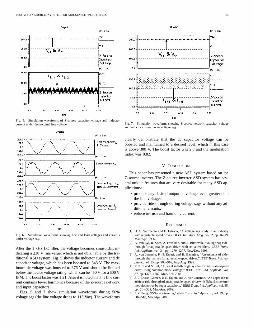
Figs. 6 and 7 show simulation waveforms during 50%voltage sag (the line voltage drops to 115 Vac). The waveforms
Fig. 7. Simulation waveforms showing Z-source network capacitor voltageand inductor current under voltage sag.
clearly demonstrate that the dc capacitor voltage can beboosted and maintained to a desired level, which in this caseis above 300 V. The boost factor was 2.8 and the modulationindex was 0.82.
V. CONCLUSIONS
This paper has presented a new ASD system based on theZ-source inverter. The Z-source inverter ASD system has sev-eral unique features that are very desirable for many ASD ap-plications:
• produce any desired output ac voltage, even greater thanthe line voltage;
• provide ride-through during voltage sags without any ad-ditional circuits;
• reduce in-rush and harmonic current.
REFERENCES
[1] H. G. Sarmiento and E. Estrada, “A voltage sag study in an industrywith adjustable speed drives,”IEEE Ind. Appl. Mag., vol. 2, pp. 16–19,Mar./Apr. 1996.
[2] A. Van Zyl, R. Spee, A. Faveluke, and S. Bhowmik, “Voltage sag ride-through for adjustable-speed drives with active rectifiers,”IEEE Trans.Ind. Applicat., vol. 34, pp. 1270–1277, Nov./Dec. 1998.
[3] A. von Jouanne, P. N. Enjeti, and B. Banerjee, “Assessment of ride-through alternatives for adjustable-speed drives,”IEEE Trans. Ind. Ap-plicat., vol. 35, pp. 908–916, July/Aug. 1999.
[4] Y. Kim and S. Sul, “A novel ride-through system for adjustable-speeddrives using common-mode voltage,”IEEE Trans. Ind. Applicat., vol.37, pp. 1373–1382, Mar./Apr. 2001.
[5] J. L. Duran-Gomez, P. N. Enjeti, and A. von Jouanne, “An approach toachieve ride-through of an adjustable-speed drive with flyback convertermodules power by super capacitors,”IEEE Trans. Ind. Applicat., vol. 38,pp. 514–522, Mar./Apr. 2002.
[6] F. Z. Peng, “Z-Source inverter,”IEEE Trans. Ind. Applicat., vol. 39, pp.504–510, Mar./Apr. 2003.