1-three phase boost rectifiereprints.uthm.edu.my/id/eprint/2905/1/rohaizan_bin_saher...viii 2.2.5...
TRANSCRIPT
THREE PHASE BOOST RECTIFIER DESIGN
ROHAIZAN BIN SAHER
A thesis submitted in partial
Fulfillment of the requirement for the award of the
Degree of Master of Electrical Power Engineering
Faculty of Electrical and Electronic Engineering
Universiti Tun Hussein Onn Malaysia
JULY 2012
v
ABSTRACT
An electric power can be converted from one form to another form by using power
electronics devices. The function of power electronics circuits by using semiconductor
devices as switch is modifying or controlling a voltage. The goal of power electronics
circuits are to convert electrical energy from one form to another, from source to load
with highest efficiency, high availability and high reliability with the lowest cost,
smallest size and weight. The term rectification refers to the power circuit whose
function is to alter the ac characteristic of the line electric power to produce a
“rectified”ac power at the load side that contain the dc value In this project, a study has
done for the two types of rectifier topology of alternating current to direct current
voltage of a three-phase boost rectifier with pulse width modulation (PWM) and a three-
phase boost rectifier with active power filter (APF). Power factor, shape distortion and
voltage can be increased as much as seen through two types of this topology if it is
connected to the non-linear loads in power systems. Three phase rectifier with pulse-
width modulation (PWM) is one of controlled rectifier consist six pulses divides into
two groups which are top group and bottom group. For top group, IGBT with its
collector at the highest potential will conduct at one time. The other two will be
reversed. Thus for bottom group, IGBT with the its emitter at the lowest potential will
conduct. This project also observes the current, voltage waveform and the harmonics
component when the active power filter (AFC) placed in series with non-linear load.
Type of rectifier used is uncontrolled rectifier. In this work MATLAB/SIMULINK
power system toolbox is used to simulate the system Results of simulations carried out,
the advantages and disadvantages, the increase in voltage and waveform distortion for
the system under consideration can be shown

vi
ABSTRAK
Kuasa eletrik boleh diubah daripada satu bentuk ke bentuk yang lain dengan
menggunakan litar peranti kuasa elektronik.Fungsi litar elektronik berkuasa dengan
menggunakan peranti semiconductor sebagai suis untuk mengawal dan mengubah arus
voltan.Matlamat litar elektronik berkuasa adalah untuk mengubah kuasa elektrik kepada
bentuk yang lain, daripada sumber kuasa kepada beban dengan tahap kecekapan yang
tertinggi, perihal boleh didapati yang tertinggi ,perihal yang dapat dipercayai tertinggi
dengan kos yang paling murah ,saiz dan berat yang paling kecil.Istilah rektifikasi
merujuk kepada litar kuasa yang berfungsi untuk mengubah ciri arus ulang alik dalam
talian kuasa elektrik untuk menghasilkan arus ulang alik pada beban yang mengandungi
nilai arus terus Dalam projek ini , kajian dilakukan bagi dua jenis topologi penerus dari
arus ulang alik kepada arus terus iaitu penerus panaik voltan tiga fasa dengan
pemodulatan lebar denyut (PWM) dan pengubah penaik voltan tiga fasa dengan penapis
kuasa aktif (APF). Faktor kuasa, bentuk herotan dan seberapa banyak voltan dapat
dinaikkan dilihat melalui dua jenis topologi ini jika ia disambungkan kepada beban
tidak linear dalam sistem kuasa. Penerus tiga fasa dengan pemodulatan lebar denyut
(PWM) adalah salah satu penerus terkawal yang mengandungi enam denyutan Ia di
bahagikan kepada dua bahagian iaitu bahagian atas dan bahagian bawah, yang mana
masing-masing mengandungi tiga komponen IGBT. Pada bahagian atas salah satu
daripada pemungut IGBT yang menerima voltan pincang hadapan akan beroperasi. Dua
lagi IGBT dalam keadaan pincang songsang. Begitu juga yang berlaku di bahagian
bawah, pemancar IGBT yang menerima voltan pincang songsang akan beroperasi.
Projek ini juga melihat arus, bentuk gelombang voltan dan komponen harmonik apabila
penapis kuasa aktif (AFC) diletakkan secara bersiri dengan beban yang tidak linear.
Jenis penerus yang digunakan adalah dari jenis penerus yang tidak dikawal. Dalam

vii kerja-kerja ini MATLAB / Simulink kuasa sistem toolbox digunakan untuk
mensimulasikan sistem. Hasil daripada simulasi yang dijalankan, kelebihan dan
kekurangan, peningkatan voltan dan herotan gelombang bagi sistem yang dikaji dapat
ditunjukkan.

vii
CONTENTS
TITLE i
DECLARATION ii
DEDICATION iii
ACKNOWLEDGEMENT iv
ABSTRACT v
ABSTRAK vi
CONTENTS vii
LIST OF TABLE ix
LIST OF FIGURE x
LIST OF SYMBOLS xii
LIST OF APPENDICS xiii
CHAPTER 1 INTRODUCTION 1
1.1 Introduction 1
1.2 Problem of Statement 2
1.3 Objective of Project 3
1.4 Scope of Study 3
1.5 Thesis Outline 4
CHAPTER 2 LITERATURE REVIEW 5
2.1 Introduction 5
2.2 Boost Derived Rectifier Topologies 5
2.2.1 Three-Phase Six Switch Boost Rectifier 5
2.2.2 Three-Phase Four Switch Boost Rectifier 6
2.2.3 Three Switch Boost Power Converter 7
2.2.4 Vienna Rectifier 8

viii
2.2.5 Single Switch Boost Power Converter 9
2.3 Boost Rectifier with Harmonic Circuit 10
2.3.1 Three-Phase, Single Switch Boost Rectifier 10
2.4 Modulation Techniques 11
2.4.1 Sinusoidal PWM 11
2.4.2 Generalized Discontinuous pulse width 12
modulation (GDPWM).
2.5 Active Power Filter 12
CHAPTER 3 METHODOLOGY 15
3.1 Introduction 15
3.2 Development of Three Phase Boost Rectifier Design 16
3.3 Operation of Three Phase Boost Rectifier 17
3.4 Model of Three Boost Rectifier 20
3.5 Active Power Filter using closed loop concept 23
3.5.1 Hyteresis Current Control 24
CHAPTER 4 SEMULATION RESULT AND ANALYSIS 26
4.1 Introduction 26
4.2 Simulation system via MATLAB/Simulink 26
4.2.1 Nonlinear Load 28
4.2.1.1 Uncontrolled Rectifier Load (Resistor) 28
4.2.1.2 Uncontrolled Rectifier Load 34
(Resistor and Inductance)
CHAPTER 5 CONCLUSIONS AND RECOMENDATIONS 39
FOR THE FUTURE WORKS
5.1 Conclusion 39
5.2 Recommendations for Future Work 40
REFERENCES 42
APPENDIX 47
ix
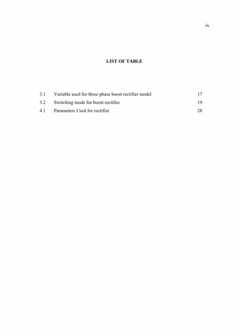
LIST OF TABLE
3.1 Variable used for three-phase boost rectifier model 17
3.2 Switching mode for boost rectifier 19
4.1 Parameters Used for rectifier 28
x
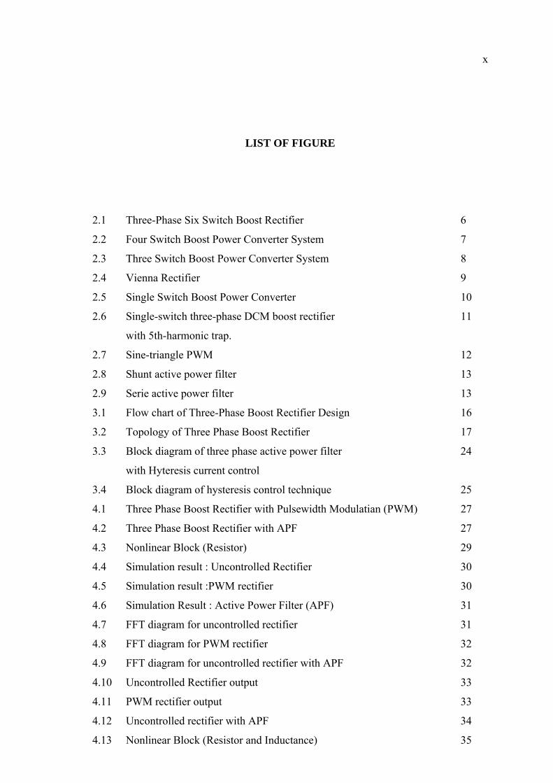
LIST OF FIGURE
2.1 Three-Phase Six Switch Boost Rectifier 6
2.2 Four Switch Boost Power Converter System 7
2.3 Three Switch Boost Power Converter System 8
2.4 Vienna Rectifier 9
2.5 Single Switch Boost Power Converter 10
2.6 Single-switch three-phase DCM boost rectifier 11
with 5th-harmonic trap.
2.7 Sine-triangle PWM 12
2.8 Shunt active power filter 13
2.9 Serie active power filter 13
3.1 Flow chart of Three-Phase Boost Rectifier Design 16
3.2 Topology of Three Phase Boost Rectifier 17
3.3 Block diagram of three phase active power filter 24
with Hyteresis current control
3.4 Block diagram of hysteresis control technique 25
4.1 Three Phase Boost Rectifier with Pulsewidth Modulatian (PWM) 27
4.2 Three Phase Boost Rectifier with APF 27
4.3 Nonlinear Block (Resistor) 29
4.4 Simulation result : Uncontrolled Rectifier 30
4.5 Simulation result :PWM rectifier 30
4.6 Simulation Result : Active Power Filter (APF) 31
4.7 FFT diagram for uncontrolled rectifier 31
4.8 FFT diagram for PWM rectifier 32
4.9 FFT diagram for uncontrolled rectifier with APF 32
4.10 Uncontrolled Rectifier output 33
4.11 PWM rectifier output 33
4.12 Uncontrolled rectifier with APF 34
4.13 Nonlinear Block (Resistor and Inductance) 35

xi 4.14 Simulation result :Uncontrolled rectifier (R-L Load) 35
4.15 Simulation result : PWM rectifier (R-L Load) 36
4 16 Simulation result: Active Power Filter (R-L Load) 36
4.17 FFT diagram for uncontrolled rectifier (R-L Load) 37
4.18 FFT diagram for PWM rectifier (R-L Load) 37
4.19 FFT diagram for uncontrolled rectifier with APF (R-L Load) 38

xii
LIST OF SYMBOLS
AC - Alternate Current
DC - Direct Current
KVL - Kirchhoff Voltage Law
KCL - Kirchhoff Current Law
APF - Active Power Filter
THD - Total Harmonic Distortion
PWM - Pulse Width Modulation
GPWM - Generalized Discontinuous Pulse Width Modulation
icompA, B C - Reference currents
PI - Proportional Integral
PLL - Phase Locked Loop
HBCC - Hysteresis Band Current control
α - Alpha
β - Beta
PFC - Power Factor Correction
PF - Power Factor
Vas,Vbs, Vcs - Input AC side voltage
Ia,Ib,Ic - Phase current
ra,rb,rc - Per phase resistance
IL - Load Current
S11, S21,S31 - Switching function on top devices
S12, S22 .S32 - Switching function on bottom devices
RL - Load resistance

xiii
LIST OF APPENDICES
APPENDIX TITLE PAGE
A Parameter for three phase boost rectifier 47
with pulsewidth modulation (PWM)
B Output Voltage (Vdc) and Power Factor 49
Calculation
C Circuit Diagram 52
D Result and Simulation 56
E Table for effects of harmonic on equipment 69
F IEEE-519 Requirements 71

1
CHAPTER 1
INTRODUCTION
1.1 Introduction
A switching power rectifier in the power system is convert one level of
electrical energy into another level of electrical energy. Converters in the AC to DC
conversion field are the most widespread [G. Chesi ,2009] and the operation of a
converter can be explained in terms of the input quantities, output quantities, and the
switching pattern used to obtain the preferred output. In industrial applications where
three-phase ac voltages are available, it is preferable to use three-phase rectifier circuits,
compared to single-phase rectifiers. Three-phase rectifiers have the following
advantages compared with single-phase rectifiers [Mohan, N., Undeland, T., and
Robbins ,1995]
a. higher output voltage for a given input voltage
b. lower amplitude ripples, i.e. output voltage is smoother
c. higher frequency ripples, simplifying filtering
d. higher power-handling capability
e. higher overall efficiency
Type of semiconductor device used in the rectifier are different following
application as [Enrique Acha ,1997] :
a. Uncontrolled rectifiers - Diodes as the switches
b. Phase-controlled rectifiers - SCR (silicon controlled rectifiers)
c. Pulse-width modulation rectifiers - IGBT.s (insulated gate bipolar
transistors) or power MOSFET.s (metal oxide field-effect transistors)
2 Among three-phase AC to DC rectifiers, boost-type topologies are frequently used
because of continuous input currents and high output voltages. The ability to control the
system to obtain unity power factor operation of a boost rectifier is important feature of
the rectifier topology. The power factor (PF) is defined as the ratio of working power to
apparent power. The power quality problems, such as large values of harmonics, poor
power factor and high total harmonic distortion, are usually associated with operation of
three phase AC to DC converters. An increase in the current harmonics and a decrease
in the displacement power factor in AC power lines produced by diode and thyristors
are a serious problem, thereby highlighting the importance of the boost rectifier in
minimizing these problems.
Active power filter (APF) or pulsewidth-modulation (PWM) rectifiers in
distribution systems represents the best solution, in terms of performance and
effectiveness, for elimination of harmonic distortion as well as power factor correction,
balancing of loads, voltage regulation and flicker compensation. Sinusoidal PWM [P.
Wood , 1981] is technique employed where the sinusoidal waveform or modulation
signal is compared with a very high frequency triangle or carrier signal to obtain the
switching pulses for the device.
The shunt APF, connected in parallel with the non-linear load, is commonly
utilized to compensate for current disturbances while the series APF is utilized to
compensate for voltage disturbances.
The aim of the project is to study an existing three-phase boost rectifier and
design a new three-phase boost rectifier topology with minimum value of current
harmonics. In this project, trends and future prospects in new three-phase boost rectifier
topology with pulsewidth modulation (PWM) and active power filter (APF) are
presented and the simulation result will be shown. A method of identification of supply
current will be developed by using MATLAB/Simulink for elimination of the
harmonics of current and to obtain a sinusoidal current of line.
1.2 Problem of Statement
From the study in this project, there are a large number of switching converter
topologies and composite switching converters are possible. The power quality
3 problems, such as large values of harmonics, poor power factor and high total harmonic
distortion, are usually associated with operation of three phase AC/DC converters
especially nonlinear load. There have been many approaches to mitigate the harmonics
in the rectifier system. They include the following:
a. active power filters;
b. six-switch pulsewidth-modulation (PWM) rectifiers;
c. power-factor correction (PFC) by boost converters;
d. multipulse rectifiers;
e. harmonic current injection method.
1.3 Objective of Project
The objective in this project is to develop and compare in term of method or topology
of three phase boost rectifier which more efficient and able to solve the nonlinear
problem with optimum way. Six-switch pulsewidth-modulation (PWM) rectifiers and
active power filter (APF) will be used in this project. The APC topology is unique
because the configuration is more reliable. A failed shunt filter does not immediately
affect the loads side.
1.4 Scope of Study
The scope of this project is to study the three phase boost rectifier characteristic and
effect of the harmonics on non linear loads. The simulation of this project is base on
three phase system with six-switch pulsewidth- modulation (PWM) and Uncontrolled
rectifier with Active Power Filter (APF) . Modeled by using MATLAB Simulink to
analysis the distorted source current waveform drawn by the nonlinear load. At the end
of this project, analyze and compare two rectifier topology in term of harmonic currents
and the d.c voltage..
4
1.5 Thesis Outline
The thesis is organized into 5 chapters namely the introduction, literature reviews,
methodology, simulations and results analysis, conclusion and recommendation.
Chapter I discuss the background and general idea of the proposed project. The
objective and scope of this project are state in this chapter.
Chapter II conducts a detailed literature survey on the previous work done in
three phase boost The chapter also includes sections on the past work done in
Pulsewidth Modulation (PWM) boost rectifier and boost rectifier with active power
filter (APF)
Chapter III details on research methodology of each design state. Two
topologies for the connection of boost rectifier; pulsewidth modulation and active power
filter are discussed in this chapter with operation of the system.
Chapter IV displays the simulation result and analyze the compensation two
different three phase boost rectifier topologies;pulsewidth modulation and active power
filter subject to a typical nonlinear load. The simulation design and the result of each
stage will be observed.
Chapter V summarizes the work done in the thesis and concludes with
suggestions for future work.
5
CHAPTER 2
LITERATURE REVIEW
2.1 Introduction
This chapter presents a review on the various works previously done on three phase
boost rectifier. A three-phase system has certain inherent advantages over a single-phase
system. In this chapter discusses the nature of three-phase rectifier and reports the
different types of three phase topologies. The topologies are discussed and various
strengths and weakness highlighted.
2.2 Boost Derived Rectifier Topologies
Three-phase boost PFC power rectifier have traditionally been the preferred
topology for high power applications due to their symmetric current drawing
characteristics. A disadvantage to any boost derived topology is the inability to control
startup inrush currents and output short circuit conditions, unless bi-directional power
flow is possible. The following subsections describe various boost derived topologies.
2.2.1 Three-Phase Six Switch Boost Rectifier
A common six switch boost rectifier topology has the ability to operate as a
rectifier as well as an inverter due to the bidirectional power flowing capabilities
6 (Figure 2.1). It also has good current quality and low EMI emissions [V. Blasko, V.
Vaura and W. Niewiadomski ,1998] . The use of bidirectional switches also results in
the ability to control the output voltage down to zero, thus, eliminating the problem that
boost topologies have with regard to startup inrush currents and output short circuit
protection. Unidirectional switches can be used for simplicity at the expense of current
control capabilities. The converter is controlled by an output voltage loop for output
regulation, and inner current loops which shape the input currents according to their
sinusoidal references. The input inductors form part of the boost topology and, as such,
work at the switching frequency. As a result, input inductors operating at switching
frequencies are smaller in size compared with line frequency input inductors.
Figure 2.1 : Three-Phase Six Switch Boost Rectifier
2.2.2 Three-Phase Four Switch Boost Rectifier
The boost derived rectifier shown in Figure 2.2 , and proposed in [Abraham
Pressman,1991] , has three boost inductors in them AC lines, four active switches and
two series connected capacitors. The boost derived rectifier is capable of bi-directional
power flow and, thus, is able to control the output voltage down to zero. The converter
performs PFC by taking advantage of the fact that if two of the three line currents in a
balanced three-phase system are controlled, the third is automatically constrained. This
7 removes the need for a third converter leg. A disadvantage is that even with a slight
imbalance in the supply system, the converter performance may deteriorate
considerably. DC-DC converter stage is still needed to provide isolation, voltage
transformation and ripple reduction.
Figure 2.2: Four Switch Boost Power Converter System
2.2.3 Three Switch Boost Power Converter
The three switch boost derived converter proposed in [S. Zheng and D.
Czarkowski,2007] works on the principle of current control. When two switches are
conducting, the phase with the larger supply voltage is connected to the positive rail,
while the phase with the smaller supply voltage is connected to the negative rail (Figure
2.3). As a result, the phase shift angle between the modulation references and supply
voltages can be at most 30o. Accordingly, this topology cannot be used for bi-directional
power flow. As a result, this topology suffers from startup inrush currents and, also,
uncontrolled negative half cycles on all phases and fluctuations in the DC bus voltage.
DC-DC converter stage is still needed to provide isolation, voltage transformation and
ripple reduction.
8
Figure 2.3 : Three Switch Boost Power Converter System
2.2.4 Vienna Rectifier
Another three-switch boost derived converter, also called the Vienna rectifier, is
a unidirectional three-level PWM converter (Figure 2.4) and, as a result, suffers from
startup inrush currents. The input stage creates a DC voltage across the two switches
connected to the transformer primary. These two switches, in turn, regulate the voltage
being applied to the primary of the transformer. Accordingly, they are able to control
the output voltage generated [D.M. Mitchell ,1980] The Vienna rectifier has a complex
control system and requires special semiconductor module fabrication.

9
Figure 2.4: Vienna Rectifier
2.2.5 Single Switch Boost Power Converter
The single switch boost converter topology proposed in [T. Nussbaumer, M.L.
Heldwein, G. Gong, S. Round, and J. Kolar,2008] has an LC type input filter and, with
the boost switch turned on at a constant frequency, the duty cycle is controlled such that
the input current is always discontinuous (Figure 2.5). During the on-period of the boost
switch, all three input phases become shorted through the input inductors, the six
rectifier diodes and the boost switch. The three input currents begin simultaneously to
increase at a rate proportional to the instantaneous values of their respective phase
voltages. The specific peak current values during each on-interval are proportional to
the average values of their input phase voltages during the same on-interval. The result
is that each AC line current is a discontinuous waveform made up of a train of triangular
pulses bounded by a sinusoidal envelope.
10
Figure 2.5 : Single Switch Boost Power Converter
2.3 Boost Rectifier with Harmonic Circuit
The quantity of input current harmonics is an important parameter to unsure the
performance of a switching mode.
2.3.1 Three-Phase, Single Switch Boost Rectifier
The single switch boost rectifier proposed in [Q. Huang and F. C. Lee,1996] to
reduce the magnitude of the 5th harmonic in the input current. The fifth-order-harmonic
trap filter, which consists of inductances and capacitance place at the input of the power
stage. The harmonic-trap inductance can be utilized as a part of the differential-mode
input filter formed by the addition of filter. One problem in using a harmonic trap in a
harmonic generating power system is the possibility to excite harmonic resonances.
Both series and parallel resonances may occur in a power system due to the existence of
the filter and power line reactive components.
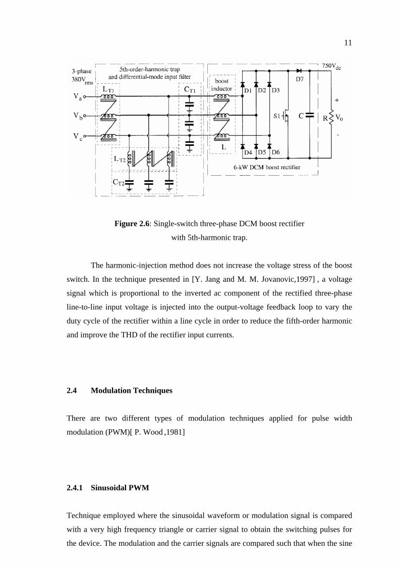
11
Figure 2.6: Single-switch three-phase DCM boost rectifier
with 5th-harmonic trap.
The harmonic-injection method does not increase the voltage stress of the boost
switch. In the technique presented in [Y. Jang and M. M. Jovanovic,1997] , a voltage
signal which is proportional to the inverted ac component of the rectified three-phase
line-to-line input voltage is injected into the output-voltage feedback loop to vary the
duty cycle of the rectifier within a line cycle in order to reduce the fifth-order harmonic
and improve the THD of the rectifier input currents.
2.4 Modulation Techniques
There are two different types of modulation techniques applied for pulse width
modulation (PWM)[ P. Wood ,1981]
2.4.1 Sinusoidal PWM
Technique employed where the sinusoidal waveform or modulation signal is compared
with a very high frequency triangle or carrier signal to obtain the switching pulses for
the device. The modulation and the carrier signals are compared such that when the sine
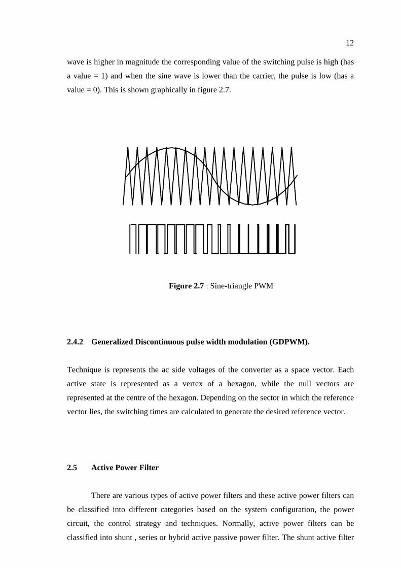
12 wave is higher in magnitude the corresponding value of the switching pulse is high (has
a value = 1) and when the sine wave is lower than the carrier, the pulse is low (has a
value = 0). This is shown graphically in figure 2.7.
Figure 2.7 : Sine-triangle PWM
2.4.2 Generalized Discontinuous pulse width modulation (GDPWM).
Technique is represents the ac side voltages of the converter as a space vector. Each
active state is represented as a vertex of a hexagon, while the null vectors are
represented at the centre of the hexagon. Depending on the sector in which the reference
vector lies, the switching times are calculated to generate the desired reference vector.
2.5 Active Power Filter
There are various types of active power filters and these active power filters can
be classified into different categories based on the system configuration, the power
circuit, the control strategy and techniques. Normally, active power filters can be
classified into shunt , series or hybrid active passive power filter. The shunt active filter
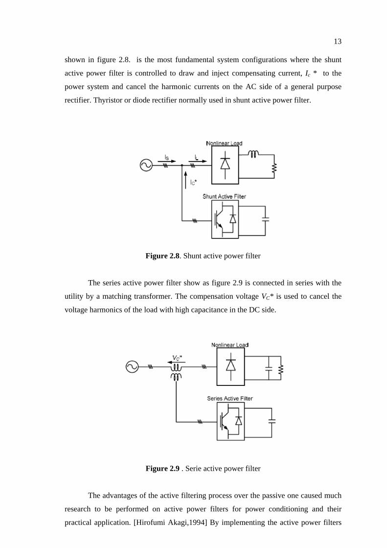
13 shown in figure 2.8. is the most fundamental system configurations where the shunt
active power filter is controlled to draw and inject compensating current, Ic * to the
power system and cancel the harmonic currents on the AC side of a general purpose
rectifier. Thyristor or diode rectifier normally used in shunt active power filter.
Figure 2.8. Shunt active power filter
The series active power filter show as figure 2.9 is connected in series with the
utility by a matching transformer. The compensation voltage VC* is used to cancel the
voltage harmonics of the load with high capacitance in the DC side.
Figure 2.9 . Serie active power filter
The advantages of the active filtering process over the passive one caused much
research to be performed on active power filters for power conditioning and their
practical application. [Hirofumi Akagi,1994] By implementing the active power filters

14 for power conditioning; it provides functions such as reactive power compensations,
harmonic compensations, harmonic isolation, harmonic damping, harmonic termination,
negative-sequence current or voltage compensation and voltage regulation. Active
power filter consists of an inverter with switching control circuit. The inverter of the
active power filter will generate the desired compensating harmonics based on the
switching gates provided by the controller. The total harmonic distortion (THD) of a
current or voltage is equal to the effective value of all the harmonics divided by the
effective value of fundamental.
The equation of a distorted current is:
Total Harmonic Distortion (THD) = (2.1)
The equation of a distorted voltage is:
Total Harmonic Distortion (THD) = (2.2)
The IEEE Standard 519-1992 specifies the maximum percentage THD permitted for
both current distortion and voltage distortion. [Theodore R.Bosela] . The THD in
voltage and current are defined as:
(2.3)
(2.4)
Where Vn an In = the amplitide of that harmonic relative to the fundamental
n = harmonic nimber
15
CHAPTER 3
METHODOLOGY
3.1 Introduction
As explained in Chapter 1, rectifiers are power electronic systems that convert input ac
power to output dc power. The operation of a converter can be explained in terms of the
input quantities, output quantities, and the switching pattern used to obtain the preferred
output. The best configuration of a boost rectifier is using pulse -width modulation
technique. The pulse-width modulated rectifiers can be further divided on the basis of
the relationship between the ratios of the input and output voltages. Boost rectifier has
an output dc voltage that is higher in magnitude than the peak value of the ac input
voltage. The switching pattern of the switches in the converter is obtained in
accordance with Kirchhoff voltage law (KVL) and Kirchhoff current law (KCL). There
are eight different switching modes for the boost rectifier. MATLAB-Simulink as the
digital simulation tool are use in this project to simulate the three phase boost rectifier
design with PWM and APF. Mastering the simulation tool and literature reviews are
done first.
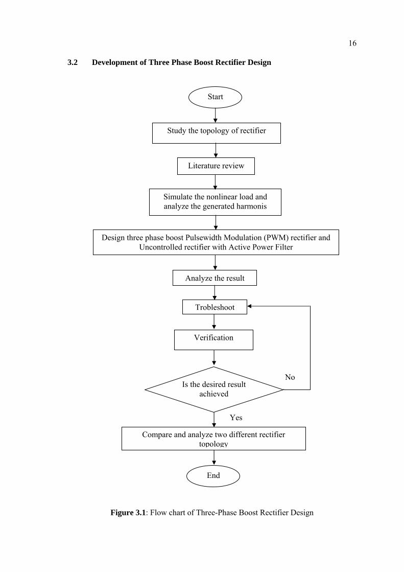
16 3.2 Development of Three Phase Boost Rectifier Design
Is the desired result achieved
Compare and analyze two different rectifier topology
End
Analyze the result
Trobleshoot
Verification
Start
Study the topology of rectifier
Literature review
Simulate the nonlinear load and analyze the generated harmonis
Design three phase boost Pulsewidth Modulation (PWM) rectifier and Uncontrolled rectifier with Active Power Filter
No
Yes
Figure 3.1: Flow chart of Three-Phase Boost Rectifier Design
17 3.3 Operation of Three Boost Rectifier
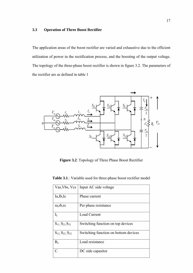
The application areas of the boost rectifier are varied and exhaustive due to the efficient
utilization of power in the rectification process, and the boosting of the output voltage.
The topology of the three-phase boost rectifier is shown in figure 3.2. The parameters of
the rectifier are as defined in table 1
Figure 3.2: Topology of Three Phase Boost Rectifier
Table 3.1.: Variable used for three-phase boost rectifier model
Vas,Vbs, Vcs Input AC side voltage
Ia,Ib,Ic Phase current
ra,rb,rc Per phase resistance
IL Load Current
S11, S21,S31 Switching function on top devices
S12, S22 .S32 Switching function on bottom devices
RL Load resistance
C DC side capasitor
18 The three-phase boost rectifier comprises of six switches that are switched using
sinusoidal pulse width modulation technique. In general, the operation of a converter
can be explained in terms of the input quantities, output quantities, and the switching
pattern used to obtain the desired output. The switching pattern of the switches in the
converter is obtained in accordance with Kirchhoffs voltage law (KVL) and Kirchhoffs
current law (KCL). The ON and .OFF. states of a single switch are assumed to have
values 0 and 1.
In a three-phase rectifier, the input ac voltages are defined and the output dc
voltage is dependent on the input quantities as well as the switching pattern of the
rectifier. The switching pattern for any converter can be expressed as a function, which
is a mathematical representation of the switching pattern, called an existence function.
[P. Wood,1981]
There are two different types of existence functions, modulated and
unmodulated. Modulated existence functions have pulses of varying widths, and
unmodulated functions have pulses of uniform width. The operating modes of the boost
rectifier are the same as that of a three-phase voltage source inverter. There are eight
different switching modes for the boost rectifier. As explained earlier the ON and OFF
states are assigned the values 1 and 0, respectively.

19
Table 3.2: Switching mode for boost rectifier
S.No S11 S21 S31
1 0 0 0
2 0 0 1
3 0 1 0
4 0 1 1
5 1 0 0
6 1 0 1
7 1 1 0
8 1 1 1
From the above eight possible switching modes, only six modes can be used in
synthesizing a dc voltage, and are called active states. The two states (1 and 8) are
called null states as these states do not result in an output dc voltage and are thereby
inactive.
Equations (3.1) to (3.3) show that at no instant of time can the top and bottom
devices of the same leg be ON simultaneously
(3.1)
(3.2)
(3.3)
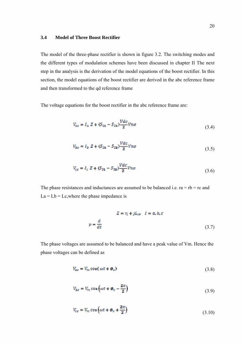
20 3.4 Model of Three Boost Rectifier
The model of the three-phase rectifier is shown in figure 3.2. The switching modes and
the different types of modulation schemes have been discussed in chapter II The next
step in the analysis is the derivation of the model equations of the boost rectifier. In this
section, the model equations of the boost rectifier are derived in the abc reference frame
and then transformed to the qd reference frame
The voltage equations for the boost rectifier in the abc reference frame are:
(3.4)
(3.5)
(3.6)
The phase resistances and inductances are assumed to be balanced i.e. ra = rb = rc and
La = Lb = Lc,where the phase impedance is
(3.7)
The phase voltages are assumed to be balanced and have a peak value of Vm. Hence the
phase voltages can be defined as
(3.8)
(3.9)
(3.10)
21 φv is the voltage phase angle and ω is the frequency of the voltage in rad/sec. Vno is
the neutral voltage
Substituting Equations (3.1) - (3.3) in (3.4) - (3.5), the voltage equations for the boost
rectifier can be expressed in terms of the switching functions of the top devices as:
(3.11)
(3.12)
(3.13)
The phase impedance Z can be substituted for in Equations (3.11) to (3.13) by
substituting equation (3.7).
(3.14)
(3.15)
(3.16)
The final state equation that completes the system model for the boost rectifier is the
capacitor voltage equation. The capacitor voltage equation for the boost rectifier is
expressed in terms of the load current IL and the dc current at the output of the rectifier
(3.17)
Where Ip the output is current defined in terms of the switching functions of the top
devices as:
22
(3.18)
Substituting equation (3.16) in (3.15)
(3.19)
The next step in the analysis is the elimination of the neutral voltage in equations 3.14
to 3.16. The neutral voltage is eliminated by adding equations (3.14) to (3.16). As the
system voltages Vas, Vbs and Vcs are balanced
Hence the neutral voltage can be expressed in terms of the switching functions as
(3.20)
Using equation (3.20), the neutral voltage can be eliminated in the voltage equations
3.14 to 3.16 resulting in
(3.21)
(3.22)
(3.23)
The simulation of the three-phase boost rectifier is using the following equations:
(3.24)

23
(3.25)
(3.26)
(3.27)
The switching functions for the rectifier are obtained by sine-triangle PWM. The
modulation signals are chosen to have a magnitude of 0.8 and the frequency of the
modulation signals (which is equal to the frequency of the supply voltages) is taken as
50Hz. The load resistance is assumed to be 50Ω
3.5 Active Power Filter using closed loop concept
Block diagram of three phase active power filter with Hysteresis current controller show
as figure 3.3 in the system configuration and design that was based on pulse-width
modulated (PWM) voltage source inverter. The filter was shunt-connected with the load
that being compensated. The basic concept is for the harmonic current cancellation so
that the current being supplied from the source was sinusoidal.
The desired compensated harmonics icompA*,icompB*and icompC *of each
phase are used as the reference currents in the system. This allows the proposed active
power filter to produce the output current, icompA, icompB and icompC according to the
reference current icompA*,icompB *and icompC *from the instantaneous active and
reactive power calculation.
The feedback current signal is the actual output current, icomp , of the inverter
which needs to be injected back into the power line. The current error signal is acquired
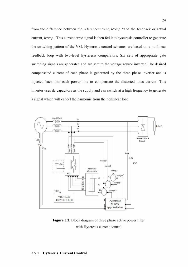
24 from the difference between the referencecurrent, icomp *and the feedback or actual
current, icomp . This current error signal is then fed into hysteresis controller to generate
the switching pattern of the VSI. Hysteresis control schemes are based on a nonlinear
feedback loop with two-level hysteresis comparators. Six sets of appropriate gate
switching signals are generated and are sent to the voltage source inverter. The desired
compensated current of each phase is generated by the three phase inverter and is
injected back into each power line to compensate the distorted lines current. This
inverter uses dc capacitors as the supply and can switch at a high frequency to generate
a signal which will cancel the harmonic from the nonlinear load.
Figure 3.3: Block diagram of three phase active power filter
with Hyteresis current control
3.5.1 Hyteresis Current Control
42
REFERENCES
G. Chesi. Estimating the domain of attraction for non-polynomial systems via LMI
optimizations. Automatica, 45(6):1536–1541, 2009.
Mohan, N., Undeland, T., and Robbins, W.: ‘Power electronics converters, applications
and design’, (John Wiley & Sons Inc, 1995)
Enrique Acha. Switching Power Supply Design. McGraw-Hill, 1997
P. Wood, Switching Power Converters, Van Nostrand Reinhold Company, 1981
V. Blasko, V. Vaura and W. Niewiadomski, “Sampling of Discontinuous Voltage and
CurrentSignals in Electrical Drives: A System Approach”, IEEE Transactions on
Industrial Applications,Vol. 34, No. 5, pp. 1123-1130, Sept. 1998.
Abraham Pressman, “Switching Power Supply Design”, McGraw-Hill Inc., 1991
S. Zheng and D. Czarkowski, “Modelling and Digital Control of a Phase-Controlled
Series-Parallel Resonant Converter”, IEEE Transactions on Industrial
Electronics, Vol. 54, No. 2, pp.707-715, April 2007.
D.M. Mitchell, “Pulsewidth Modulator Phase Shift”, IEEE Transactions on Aerospace
Electronics, Vol. AES-16, No. 3, pp. 272-278 May 1980.
T. Nussbaumer, M.L. Heldwein, G. Gong, S. Round, and J. Kolar, “Comparison of
PredictionTechniques to Compensate Time Delays Caused by Digital Control of
a Three-Phase Buck-Type PWM Rectifier System”, IEEE Transactions on
Industrial Electronics, Vol. 55, No. 2, Feb. 2008.
43 Q. Huang and F. C. Lee, “Harmonic reduction in a single-switch, three phase boost
rectifier with high order harmonic injected PWM,” in Conf. Rec. IEEE
PESC’96, 1996, pp. 1266–1271.
Y. Jang and M. M. Jovanovic, “A novel, robust, harmonic injection method for single-
switch, three-phase, discontinuous-conduction-mode boost rectifiers,” in Conf.
Rec. IEEE PESC’97, 1997, pp. 469–475
B. K. Bose, Power Electronics and Variable Frequency Drives, IEEE Press,
Piscataway, NJ, 1996
Chua, Leon. O, Linear and Nonlinear Circuits, McGraw-Hill, New York, 1987
S.Fukuda and K. Koizumi, . Optimal Control of a Three Phase Boost Rectifier for Unity
Power Factor and Reduced Harmonics,. Proc International Conference Power
Electronics and Drive Systems, vol. 1, pp. 34-39, February 1995.
Olorunfemi Ojo, Olufemi Osaloni, Parag Kshirsagar, . The Generalized Discontinuous
PWM Modulation Scheme for Theree-Phase Voltage Source Inverters,. Proc
IEEE IECON 2003 Annual Conference, Vol 2. pp.1629-1636, 2005.
Q. Huang, F.C. Lee, Harmonic reduction in a single-switch, three-phase boost rectifier
with high order harmonic injected PWM, in: Proceedings of the IEEE, PESC
Conference, Baveno, Italy, 1996, pp. 1266–1271.
J.W. Kolar, H. Ertl, F. Zach, Space vector-based analytical analysis of the input current
distortion of a three-phase discontinuous-mode boost rectifier system, in:
Conference on Record IEEE PESC, 1993, pp. 696– 703.
A.Ueda, Y. Ito, Y. Kurimoto, A. Torii, Boost type three-phase diode rectifier using
current resonant switch, in: Conference Record IEEE, Power Conversion
Conference, vol. 1, PCC Osaka, 2002, pp. 13– 18.
44 T.S. Key, J.-S. Lai, IEEE and International Harmonic Standards Impact on Power
Electronic Equipment Design, IEEE, IECON, New Orleans, USA, 1998, pp.430-
436.
P. Barbosa, F. Canales, J.-C. Crebier, F.C. Lee, Interleaved three-phase boost rectifiers
operated in the discontinuous conduction mode: analysis, design considerations
and experimentation, IEEE Trans. Power Electron. PE-16 (5) (2001) 724–734
SGS-Thomson Microelectronics, "Power Switching Regulators," Designer's Booklet,
1st edition,September 1993
C. Zhou, Design and Analysis of an Active Power Factor Correction Circuit, M. S.
Thesis, Virginia Polytechnic Institute and State University, Sept. 1989
M. J. Kocher, R. L. Steigerwald, "An AC-to-DC Converter with High Quality Input
Waveforms," IEEE Trans. on Industry Applications, Vol. 1A-19, No. 4,
July/August, 1983, pp. 586-599
E Acha,V.G.Agelidis,O.Anaya-Lara,T.J.E. Miller,(2002). ”Power Electronic Control in
Electrical Systems”,Planta Tree,Newnes , pp. 27, 72
Emílio F. Couto, Júlio S. Martins, João L. Afonso, Simulation Results of a Shunt Active
Power Filter with Control Based on p-q Theory, Department of Industrial
Electronic University of Minho
H. Doğan, R. Akkaya, (March 18 - 20, 2009).” A Simple Control Scheme for Single-
Phase Shunt Active Power Filter with Fuzzy Logic Based DC Bus Voltage
Controller”, Proceedings of the International Multi Conference of Engineers
and Computer Scientists 2009 Vol IIIMECS 2009, Hong Kong
Mohan,N,Undeland, T and Robbins, W(1995).Power Electronics-Converters,
Application, and Design. 2nd.edition. Canada:John Wiley & Sons, Inc.
Moleykutty George and Kartik Prasad Basu,(2008). “Three-Phase Shunt Active Power
Filter”, American Journal of Applied Sciences 5 (8): pp.909-916
45 M. Rastogi, R. Naik, and N. Mohan, “A comparative evaluation of harmonic reduction
techniques in three-phase utility interface of power electronic loads,” in IEEE,
/AS Ann. Meet., Con$ Rec., 1993,
N. Mohan, M. Rastogi, and R. Naik, “Analysis of a new power electronics interface with
approximately sinusoidal 3-phase utility currents and a regulated dc output,”
IEEE Trans. Power Delivery, pp. 540-546, Apr. 1993.
Mohan, N., Undeland, T., and Robbins, W.: ‘Power electronics– converters,
applications and design’, (John Wiley & Sons Inc, 1995)
Chung, D.W., and Sul, S.K.: ‘Minimum-loss strategy for three-phase PWM rectifier’,
IEEE Trans. Ind. Electron., 1999, 46, (3), pp. 517–526
Alexa, D., and Lazar, A.: ‘Optimisation of PWM Techniques with Partially Constant
Modulating Waves’, Electr. Eng., 2000, 82, (5), pp. 263–272
M. P. Kazmierkowski, R. Krishnan, and F. Blaabjerg, Control in Power Electronics.
San Diego, CA: Academic, 1999
Y. Sato and T. Kataoka, “A current-type PWM rectifier with active damping function,”
IEEE Trans. Ind. Appl., vol. 32, no. 3, pp. 533–541, May/Jun. 1996.
M. H. Bierhoff and F. W. Fuchs, “The generically equal harmonic behavior of three
phase PWM voltage and current source converters,” in Proc. Power Electron.
Intell. Control Energy Conserv., Warsaw, Poland, 2005
Ashish Tewari,(2002). Modern Control Design with MATLAB and Simulink, British
Library Cataloguing in Publication Data.
JOs Arrillaga, Neville R Watson,(2003). ”power system Harmonics”, University of
Canterbury, Christchurch, New Zealand, Wiley, second edition, pp. 156-168
E. L. Owen, “A history of harmonics in power systems,” IEEE Ind. Appl. Mag., vol. 4,
no. 1, pp. 6–12, Jan./Feb. 1998

46
H. Fujita and H. Akagi, “A practical approach to harmonic compensation in power
systems—Series connection of passive and active filters,” IEEE Trans. Ind.
Appl., vol. 27, no. 6, pp. 1020–1025, Nov./Dec. 1991
J. C. Salmon, “3-phase pwm boost rectifier circuit topologies using 2-level and 3 level
asymmetrical half-bridges,” in Proc. IEEE APEC’95, 1995, pp. 842–848.