1. study of a power supply - physics.iitd.ac.inphysics.iitd.ac.in/experiments/power_source.pdf ·...
TRANSCRIPT

1.
Study of a power supply
1.1 Introduction
A car battery can supply 12 volts. So can 8 dry cells in series. But noone would consider using the dry cells to start a car. Why not? Obviously,the dry cells cannot supply the large current required to start the car. Thepoint is that the resistance of the source for the car battery(∼ 0.1 ohm)is considerably smaller than that for the 8 dry cells(∼ 5 to ∼ 70 ohms) inseries∗.A power supply which happens to be another commonly used sourcein the laboratory has a widely varying resistance; for a regulated power supplyit may be as small as 0.1 ohm. A source of emf figure 1.1(a) ,therefore, mustbe represented not just by its voltage Vs but by its source resistance Rs as wellfigure 1.1(b). It is convenient to think of the source Vs and its resistance Rs
as enclosed in an imaginary box(indicated by the dotted line in figure 1.1(b)with terminals A and B, which we can put to any use we like. Electricalnetworks may be complicated but it is often very useful to think of parts ofit as a ’box’ with certain parameters associated with it-in the above case theparameters being Vs and Rs.
* There are, of course, many other factors that dictate practical use of a power source.Consideration of cost, convenience of use, rechargeability, available power and energy etc.are some of these. For example, a dry cell may give only a few watt-hours of energy andcannot be recharged whereas a car battery can give 500 watt-hours and, with care, canbe recharged any number of times. A power supply, on the other hand, derives its powercontinuously from the a.c. mains and hence needs no charging and can deliver any amountof energy. We shall however, not discuss these factors here, important as they are.

16 PYP100: First Year B.Tech. Physics Laboratory IIT Delhi
Figure 1.1:
Suppose we are given such a box with terminals A and B and we have todetermine Rs and Vs. First let us see how to do this in principle, We connect avoltmeter of very high resistance(ideally infinite) so that it draws no current.It will measure Vs directly. We can now connect an ammeter(ideally zeroresistance) and measure the current which will be
i = Vs/Rs (1.1)
Thus, we may define the source resistance as the open circuit voltagebetween A and B divided by the current when A and B are short-circuited.In practice, we may have to exercise caution since the short circuit currentmay be very large and damage the instrument or the source itself.
We may now adopt the following attitude. The terminals A and B providea certain source of voltage Vs with a source resistance Rs. Actually, Rs mayinclude other circuit elements as well. For example, think of the arrangements

Power supply characteristics 17
Figure 1.2:

18 PYP100: First Year B.Tech. Physics Laboratory IIT Delhi
in figure 1.1(a) and figure 1.1(b). For these too we can represent the ’source’by a certain output voltage Vs and source resistance Rs as shown in figure1.1(b). For the case of figure1.1(a) Ohm’s law gives us
Vs = VoRs
R1 +R2
, Rs =R1R2
R1 +R2
(1.2)
We can now say that we have a source of output voltage Vs across the termi-nals AB, with an effective resistance Rs. This effective source resistance Rs
is often called the output resistance of the device as seen from AB. We shalldevelop the above ideas with a few simple experiments.
Figure 1.3: The network board

Power supply characteristics 19
1.2 The Network Board-1
The network board for our experiment is shown in Plate 1. It contains threegroups of resisters R1,R2,R3, each group having several different resistors tochoose from. It has a d-c milliammeter and a d-c voltmeter. Figure 1.3shows the details of connections provided underneath the board. It will beseen that one could choose any one resistor from group R1 and any one fromgroup R2 to make up a ’source’ like that in figure 1.1(a). The third set ofresistors R3 are all connected in series and can be used as load. One couldplug-in at any pair of points and get the desired value of the load.
1.3 Experiment A
To obtain the output voltage and output resistance of a givensource.
Figure 1.4:
Let the dotted ’box’ in the figure 1.4 with AB for its output terminals beour ’source’. As can be seen from the figure, in fact it consists of a powersupply of voltage Vo and a potential divider arrangement made of resistors R1
and R2. We have to measure its output voltage across AB and then calculateits output resistance Rs.

20 PYP100: First Year B.Tech. Physics Laboratory IIT Delhi
Vs is measured by connecting the voltmeter directly across AB. Of course,it is implied here that the resistance of the voltmeter is so large that thecurrent flowing through it can be neglected.
Now connect a resistor RL called load resistor along with a milliammeter.The current i drawn from the source is measures by the millimammeter andthe new voltmeter reading VL would be lower than Vs. If Rs be the outputresistance of the source then
Vs − iRs = VL (1.3)
Thus the output resistance Rs is given by
Rs =Drop in output voltage
Load current=Vs − VL
i(1.4)
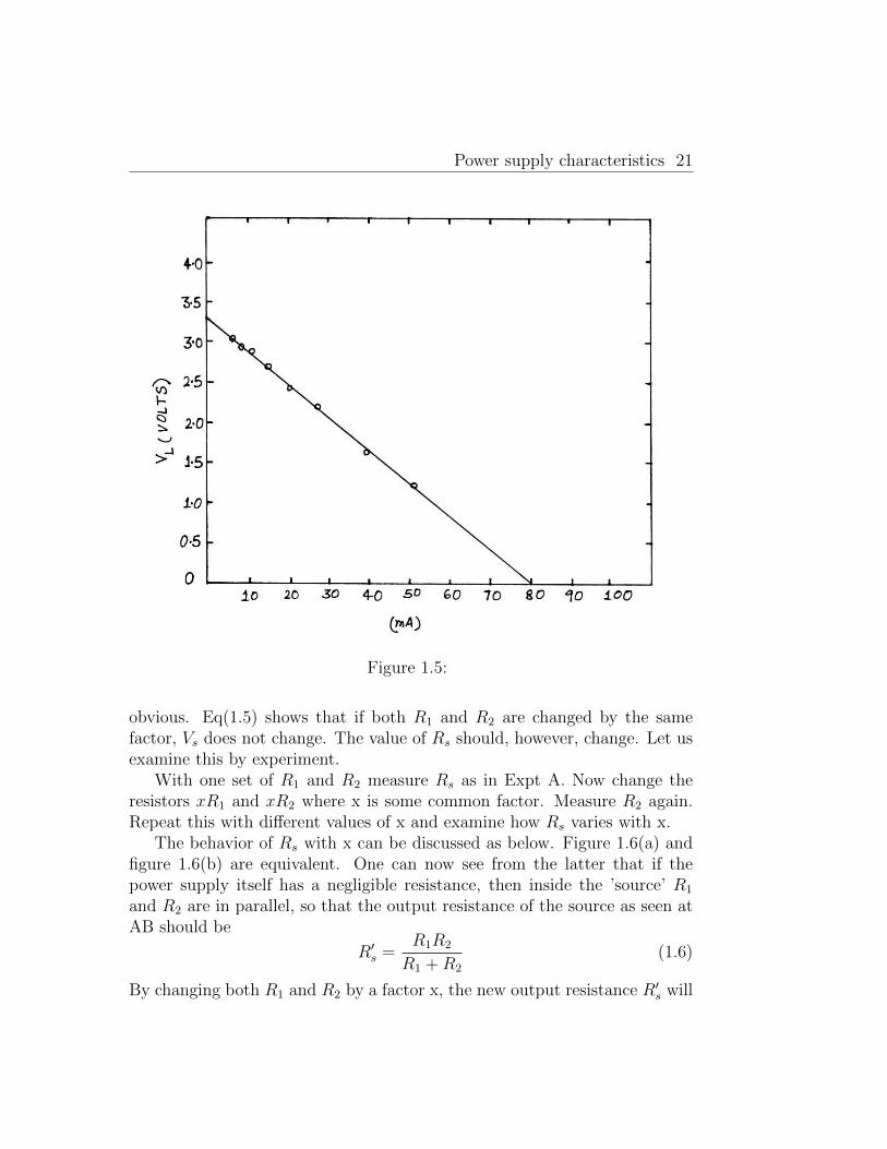
If we take several different values of RL, we shall be drawing different currentsi. The voltage drop Vs − VL will also correspondingly change. You maytabulate these values, compute Rs each time from eq(1.4), and obtain themean Rs. Alternatively, you may draw a graph between VL and i as shownin figure 1.5, see if it is a straight line, and obtain Rs from its slope and Vsfrom its intercept on the VL axis (since i=0 for this intercept Vs would be thesame as VL) Can you appreciate why it is much better to calculate Rs fromthe graph rather than directly from your observations ?
Represent your results V − s,R − s with a diagram like that in figure1.1(b). This would be the ’equivalent circuit’ for the actual source in fig 1.4.
1.4 Experiment B
To study the variation of the output resistance Rs with changes invalues of R1 and R2, the ratio R1/R2 remaining constant.
In the arrangement of figure 1.4, if the power supply is of voltage Vo andresistance zero, then by ohm’s law the output voltage across AB should be
Vs = VoR2
R1 +R2
(1.5)
You may check the measured Vs against the value calculated from eq(1.5).The dependence of the value of the output resistance Rs on R1 and R2 is
Power supply characteristics 21
Figure 1.5:
obvious. Eq(1.5) shows that if both R1 and R2 are changed by the samefactor, Vs does not change. The value of Rs should, however, change. Let usexamine this by experiment.
With one set of R1 and R2 measure Rs as in Expt A. Now change theresistors xR1 and xR2 where x is some common factor. Measure R2 again.Repeat this with different values of x and examine how Rs varies with x.
The behavior of Rs with x can be discussed as below. Figure 1.6(a) andfigure 1.6(b) are equivalent. One can now see from the latter that if thepower supply itself has a negligible resistance, then inside the ’source’ R1
and R2 are in parallel, so that the output resistance of the source as seen atAB should be
R′s =R1R2
R1 +R2
(1.6)
By changing both R1 and R2 by a factor x, the new output resistance R′s will

22 PYP100: First Year B.Tech. Physics Laboratory IIT Delhi
be given by
R′s =xR1.xR2
xR1 + xR2
=xR1R2
R1 +R2
= xRs (1.7)
Thus for a given ratio of R1/R2 i.e. for a given ratio of Vs/V0, the outputresistance comes out to be proportional to x.
Using Ohm’s law, deduce an expression for the current i drawn by a loadRL connected across AB in figure 1.6(a). Use this result to obtain expressionsfor Vs and Rs.
1.5 Experiment C
To study the power delivered by a source at different loads
A load resistor, connected across the terminals of a ’source’, draw somecurrent from it and thus consumes the power delivered to it by the ’source’.It is interesting to study how the latter varies with the load. If, for a certainload RL, the current is i, the voltage across the load is VL, then the power Pdelivered by the ’source’ is given by
P = VLi (1.8)
Connect different resistors RL and measure current i and voltage VL eachtime figure 1.7. Tabulate these data and compute the power P using eq(1.8).Also plot against RL and draw a smooth curve through the observation pointsfigure 1.8.
The curve has a broad maximum for some value of RL. What is so specialabout this particular load? If you measure the output resistance Rs of thesource(Expt. A) you will find that the power delivered is maximum whenthe load RL has the same value as Rs.
1.6 Experiment D
To learn more about ’load matching’ and power dissipation in acircuit
We have already seen in Expt B how for a given ratio of R1/R2, theoutput voltage Vs does not depend on the individual values of R1 and R2

Power supply characteristics 23
whereas the output resistance Rs does. Using this knowledge try differentarrangements of R1 and R2. Measure the output resistance Rs in each case(Expt A). Also measure the variation of the power P delivered to the loadRL for each value of Rs.
Plot the following quantities as a function of the load; (a) the load cur-rent i (b) the voltage VL across the load (c) the power dissipated in the load(d) the fraction of power dissipated in the load upon power expended by thesource. You will see that maximum power is delivered when the load RL isequal to the output resistance Rs. This disarmingly simple result is of greatimportance and you will come across it again and again in various forms.The idea is that the load resistance should match the output resistance formaximum power transfer∗. You will also notice that the current i is maxi-mum when RL is zero, the voltage VL across the load is maximum when RL isinfinite but the power iVL dissipated in the load is maximum when RL = Rs
and is equal to V 2s /4Rs. Remember, this is not the power expended by the
source which is V 2s /2Rs.
A source of output voltage Vs and output resistance Rs when connected acrossa load RL gives a current i = Vs
Rs+RLand delivers power to the load directly
given by P = i2RL Show, using differential calculus, that P is maximum whenRL = Rs.
1.7 Experiment E
To study the reflected load resistance in a network**Consider figure 1.9(a). When RL is not connected, let the current through
the circuit be i. On connecting RL, this current increases to some value iowhich means that the load RL connected across AB increases the currentfrom i to io.
We can achieve the same result if we connect a suitable load R′L across
*This statement is true for alternating current circuits also. There we talk of outputimpedance instead of output resistance and the principle assumes its general name-theprinciple of impedance matching.
**For doing this experiment, you will need a resistance box in addition to the NetworkBoard as shown in figure 1.3. Also note that in experiment on reflected load resistancemeasurement a power supply with an output voltage Vo and negligible output resistanceis used as the source.

24 PYP100: First Year B.Tech. Physics Laboratory IIT Delhi
CD(which means directly across the power supply). This load R′L seen bythe source is called as the reflected load resistance.
For the simple circuit shown in figure 1.9 you can also calculate the re-flected load resistance RL by applying Ohm’s law but in more complex net-works such calculations may not be all that simple. Nevertheless, the factremains that for a load RL across any two points(AB) in a network, simpleor complex, you can always determine the reflected load R′L as seen by thepower supply(across CD). In this sense therefore, the network acts as a ’trans-former’. It is usually called an impedance transformer when the network hascomponents other than pure resistance also.
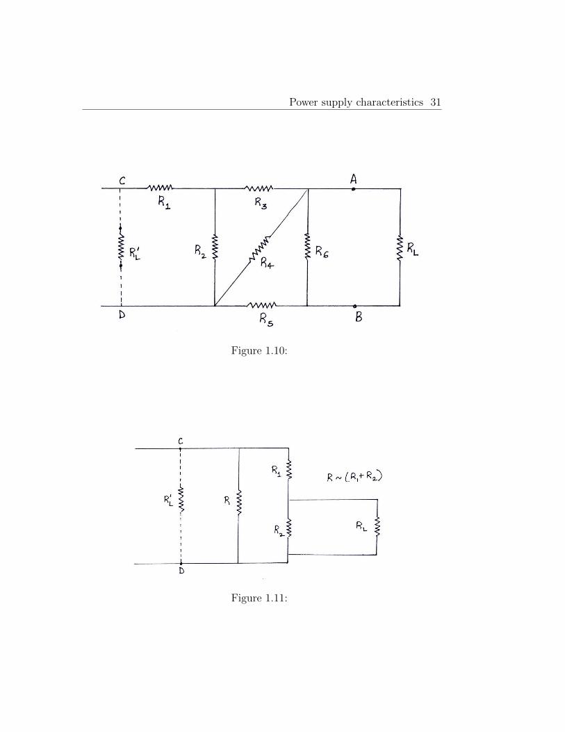
More generally, we can replace the actual load RL by a load R′L in an-other part of the circuit such that the current drawn from the source is thesame. One then calls R′L as the transfer load(transfer resistance or transferimpedance as the case may be). An example of this is shown in figure1.10.
Deduce an expression for the current in figure 1.9(a) when RL is con-nected. Deduce a similar expression for the case of figure 1.9(b) when R′Lis connected. Hence, obtain an expression for the reflected load resistance.Draw conclusions for the limiting cases of RL →∞ and R′L →∞
In the study of complicated circuits impedance transformations lead toconsiderable simplicity of analysis and are widely resorted to. We should,therefore, try to see this atleast in a simple circuit like the one shown infigure 1.11.
Use a resistance box for RL along with the network board for this experi-ment. First keep R′L =∞(plug off) and read the current in the milliammeterwhen RL = ∞ and when RL has a given value. Let these readings be i andio. Now set RL = ∞, plug-in R′L and adjust its value such that the currenthas a value of io. Read the value of R′L at this stage.
Keeping R1,R2 and R unchanged, take different values of load RL and foreach case experimentally obtain the transfer load. It may be worthwhile toplot R′L against RL and see how it varies with RL.
In the circuit of figure 1.9(a), the load RL, on being connected across theoutput terminals AB, increases current from i to io. Show that the transferload(reflected resistance) R′L as seen at CD is given by R′L = Vs
io−i where Vs isthe output voltage at AB. (Thus R′L can be deduced from measurements i,iounlike the method of direct substitution suggested in Expt E)

Power supply characteristics 25
1.8 Experiment F
To make a simple equivalent circuit for a power ’source’ ***In Experiment A, you took a simple source figure 1.4 of output voltage
Vs and output resistance Rs. Now you may take a far more complicatedarrangement, like the one shown in figure 1.12(a) and measure its V − sand the series resistance is adjusted to be RS. This is an ’equivalent circuit’corresponding to the circuit of figure 1.12(a). We may check this equivalencedirectly by experiment.
Make any network and choose any two points AB in that network as the’output terminals’. Apply different loads RL at these terminals and eachtime measure the current i drawn and the voltage VL across AB. From thesecalculate Vs and Rs as in Expt A. Now take a power-supply and adjust itsvoltage to the value Vs. Connect a resistor of value Rs in series with it Figure1.12(b). Then apply the same loads RL across its output terminals AB andeach time measure i and VL. Compare these results with those obtained withthe complicated network and see if the equivalence is complete.
Even when there is more than one source of emf in the network, theequivalence holds. In a-c circuits, with inductors and capacitors also present,the equivalence involves some more details, but is still a very useful concept.
*** This could be done immediately after Expt A as an exercise to see how any’source’(with whatever complicated details) can be replaced by an equivalent circuit of anemf Vs and a series resistance Rs. You would need some extra resistors in addition to yourNetwork Board for doing this experiment

26 PYP100: First Year B.Tech. Physics Laboratory IIT Delhi
APPENDIXCarbon Resistors
Carbon, either alone or in combination with other materials, is used in mak-
ing a class of resistors which are commonly used in radio and other com-munication circuits. After the advent of transistors and integrated circuitswhere one seldom handles large power, their use has gone up phenomenally.The commonest form of mass-produced resistors is the composition resistor,in which the conducting material, graphite or some other form of carbon,is mixed with fillers that serve as diluents and combined with an organicbinder. Two general types of composition resistors are the solid body, whichis moulded or extruded, and the filament type, in which carbon is baked ona glass or a ceraminc rod and sealed in a ceramic or bakelite tube.
Composition resistors of the usual type are, however, notoriously unstablein resistance values. If they are used only at a low power level, the changein resistance results principally from the effect of humidity on the unit. Ifoperated near the rated load, the changes in resistance result primarily fromdecomposition of the organic binder.
Much better stability is found in a special film type of resistor known as apyrolitic or ”cracked carbon” resistor. Such resistors are made by depositingcrystalline carbon at a high temperature on a ceramic rod by ”cracking”an appropriate hydrocarbon. In one process for making these film resistors,carbon is deposited from methane gas in a nitrogen atmosphere from whichwater vapour and oxygen are carefully excluded. No binder is used, and thecarbon deposits consist of a hard gray crystalline form from which graphiteand carbon black are completely absent. After the deposit is formed, theresistor is adjusted to its required value by cutting a helical groove aroundthe cylinder with a diamond impregnated copper wheel. This removes part ofthe deposit and leaves a helical conductor of a suitable length and width forthe desired resistance. After terminals are applied by a suitable process, thesurface of a resistor is lacquered with some silicon type of varnish to provideinsulation, moisture resistance and mechanical protection. These are thensorted out by measurement with a bridge in series having a tolerance of 10%or 5% or less.
For 1 watt 10k resistors of this type, a typical temperature coefficient is-0.02% per ◦C (minus sign indicates a decrease of resistance with increase intemperature unlike the wire-wound resistors) and for a 5megaohm resistor

Power supply characteristics 27
this figure is -0.04% per ◦C.There are some other advantages in using these film resistors. Their
compactness of shape and size renders them easier to handle and suitable tofit in a small space. They are avilable over a wide range of resistance(from1 ohm to 1000megaohms or more). The 10% series are available in valuesstarting from 1 ohm in a geometric progression of about 1.5 namely, 1, 1.5,2.2, 3.3, 4.9... ... .... Similarly the values in the 5% series are in a geometricprogression of 1.2 namely, 1, 1.2, 1.5, 1.8, 2.2... ... ... The resistance valuesare sometimes marked with colour bands. The colour code is-
Black 0, Brown 1, Red 2, Orange 3, Yellow 4, Green 5, Blue 6, Violet 7,Gray 8.
A simple way to remember this is the mnemonic - B.B. Roy Goes toBombay Via Gateway [Perhaps you could make a better one].
You will notice four coloured bands, three narrow and one broad, on suchresistors. The first two narrow ones, represent the first two numbers, and thethird represents the number of zeroes after two numbers. The three narrowbands thus give the value of the resistance. the (fourth) broad one represent-ing the tolerance is either a silver or a gold band, the former for 10% and thelatter for 5%. Suppose on a resistor the colour bands are like this. Brown,Gray, Red and Gold. This would mean a value of 1800 i.e. 1.8k with 5%tolerance.
REFERENCE
1.Blackburn, Components Handbook, Vol. 172.M.I.T Radiation Laboratory, Mc Graw Hill, 1949.

28 PYP100: First Year B.Tech. Physics Laboratory IIT Delhi
Figure 1.6:

Power supply characteristics 29
Figure 1.7:
Figure 1.8:

30 PYP100: First Year B.Tech. Physics Laboratory IIT Delhi
Figure 1.9:
Power supply characteristics 31
Figure 1.10:
Figure 1.11:

32 PYP100: First Year B.Tech. Physics Laboratory IIT Delhi
Figure 1.12: