1. overview analog discovery 2 reference manual analog discovery 2 reference manual written by...
TRANSCRIPT
1/24
Analog Discovery 2 Reference ManualWritten by Mircea Dabacan, PhD, Technical University of Cluj-Napoca Romania
1. OverviewThe Digilent Analog Discovery 2™, developed in conjunction with Analog Devices®, is a multi-function instrument that allows users to measure, visualize, generate,record, and control mixed signal circuits of all kinds. The low-cost Analog Discovery 2 is small enough to fit in your pocket, but powerful enough to replace a stack oflab equipment, providing engineering students, hobbyists, and electronics enthusiasts the freedom to work with analog and digital circuits in virtually anyenvironment, in or out of the lab. The analog and digital inputs and outputs can be connected to a circuit using simple wire probes; alternatively, the AnalogDiscovery BNC Adapter and BNC probes can be used to connect and utilize the inputs and outputs. Driven by the free WaveForms software, the Analog Discovery2 can be configured to work as any one of several traditional instruments, which include:
Two-channel oscilloscope (1MΩ, ±25V, differential, 14-bit, 100Msample/sec, 30MHz+bandwidth - with the Analog Discovery BNC Adapter Board)Two-channel arbitrary function generator (±5V, 14-bit, 100Msample/sec, 12MHz+bandwidth - with the Analog Discovery BNC Adapter Board)Stereo audio amplifier to drive external headphones or speakers with replicated AWGsignals16-channel digital logic analyzer (3.3V CMOS, 100Msample/sec)1) 2)
16-channel pattern generator (3.3V CMOS, 100Msample/sec)3) 4)
16-channel virtual digital I/O including buttons, switches, and LEDs – perfect for logictraining applications 5) 6)
Two input/output digital trigger signals for linking multiple instruments (3.3V CMOS)7)
Two programmable power supplies (0…+5V , 0…-5V). The maximum available outputcurrent and power depend on the Analog Discovery 2 powering choice:250mW max for each supply or 500mW total when powered through USB700mA max or 2.1W max for each supply when using an external wall power supplySingle channel voltmeter (AC, DC, ±25V)Network analyzer – Bode, Nyquist, Nichols transfer diagrams of a circuit. Range: 1Hz to10MHzSpectrum Analyzer – power spectrum and spectral measurements (noise floor, SFDR,SNR, THD, etc.)Digital Bus Analyzers (SPI, I²C, UART, Parallel)
The Analog Discovery 2 was designed for students in typical university-based circuits and electronics classes. Its features and specifications, as well as the additionalrequirements of operating from USB or external power, maintaining the small and portable form factor, the robustness to withstand student use in a variety ofenvironments, and low-cost are based directly on feedback that was obtained from numerous professors from several universities. Meeting all of these requirementsproved challenging; however, the task ultimately generated some new and innovative circuits. This document describes the Analog Discovery 2's circuits, with theintent of providing a better understanding of its electrical functions, operations, and a more detailed description of the hardware’s features and limitations. It is notintended to provide enough information to enable complete duplication of the Analog Discovery 2, or to allow users to design custom configurations forprogrammable parts in the design.
Analog Discovery 2 is the next generation of the very popular Analog Discovery. The main improvements are:
Ability to use an external power supply and consequently deliver more power to user supplies. When USB-powered, the Analog Discovery 2 delivers the samepower as the Analog Discovery.New enclosure with enhanced design and improved connector reliability.Improved signal/noise and crosstalk performances for both the scope and waveform generator.Better defined bandwidth for both the scope and waveform generator.
1.1 Architectural Overview and Block Diagram
Analog Discovery 2's high-level block diagram is presented in Fig. 2 below. The core of the Analog Discovery 2 is the Xilinx® [http://www.xilinx.com/] Spartan®-6[http://www.xilinx.com/products/silicon-devices/fpga/spartan-6/index.htm] FPGA (specifically, the XC6SLX16-1L device). The WaveForms application automaticallyprograms the Discovery’s FPGA at start-up with a configuration file designed to implement a multi-function test and measurement instrument. Once programmed,the FPGA inside the Discovery communicates with the PC-based WaveForms application via a USB 2.0 connection. The WaveForms software works with the FPGAto control all the functional blocks of the Analog Discovery 2, including setting parameters, acquiring data, and transferring and storing data.
Signals in the Analog Input block, also called the Scope, use “SC” indexes to indicate they are related to the scope block. Signals in the Analog Output block, alsocalled AWG, use “AWG” indexes, and signals in the Digital block use a D index – all of the instruments offered by the Discovery 2 and WaveForms use the circuitsin these three blocks. Signal and equations also use certain naming conventions. Analog voltages are prefixed with a “V” (for voltage), and suffixes and indexes areused in various ways: to specify the location in the signal path (IN, MUX, BUF, ADC, etc.); to indicate the related instrument (SC, AWG, etc.); to indicate the channel(1 or 2); and to indicate the type of signal (P, N, or diff). Referring to the block diagram in Fig. 2 below:

2/24
The Analog Inputs/Scope instrument block includes:Input Divider and Gain Control: high bandwidth input adapter/divider. High or low-gain can be selected by the FPGABuffer: high impedance bufferDriver: provides appropriate signal levels and protection to the ADC. Offset voltage is added for vertical position settingScope Reference and Offset: generates and buffers reference and offset voltages for the scope stagesADC: the analog-to-digital converter for both scope channels.
The Arbitrary Outputs/AWG instrument block includes:DAC: the digital-to-analog converter for both AWG channelsI/V: current to bipolar voltage convertersOut: output stagesAudio: audio amplifiers for headphone
A precision Oscillator and a Clock Generator provide a high quality clock signal for the AD and DA converters.The Digital I/O block exposes protected access to the FPGA pins assigned for the Digital Pattern Generator and Logic Analyzer.The Power Supplies and Control block generates all internal supply voltages as well as user supply programmable voltages. The control block also monitorsthe device power consumption for USB compliance when power is supplied via the USB connection. When external power supply is used, the control blockallows more power for the user supplies. Under the FPGA control, power for unused functional blocks can be turned off.The USB Controller interfaces with the PC for programming the volatile FPGA memory after power on or when a new configuration is requested. After that,it performs the data transfer between the PC and FPGA.The Calibration Memory stores all calibration parameters. Except for the “Probe Calibration” trimmers in the scope Input divider, the Analog Discovery 2includes no analog calibration circuitry. Instead, a calibration operation is performed at manufacturing (or by the user), and parameters are stored in memory.The WaveForms software uses these parameters to correct the acquired data and the generated signals
In the sections that follow, schematics are not shown separately for identical blocks. For example, the Scope Input Divider and Gain Selection schematic is onlyshown for channel 1 since the schematic for channel 2 is identical. Indexes are omitted where not relevant. As examples, in equation 4 below, V indiff does not containthe instrument index (which by context is understood to be the Scope), nor the channel index (because the equation applies to both channels 1 and 2). In equation 3,the type index is also missing because Vmux and V in refer to any of P (positive), N (negative) or diff (differential) values.
Figure 2. Analog Discovery 2 block diagram.
2. ScopeImportant Note: Unlike traditional inexpensive scopes, the Analog Discovery 2 inputs are fully differential. However, a GND connection to the circuit under test is needed to provide a stablecommon mode voltage. The Analog Discovery 2 GND reference is connected to the USB GND. Depending on the PC powering scheme, and other PC connections (Ethernet, audio, etc. – whichmight also be grounded) the Analog Discovery 2 GND reference might be connected to the whole GND system and ultimately to the power network protection (earth ground). The circuit under testmight also be connected to earth or possibly floating. For safety reasons, it is the user’s responsibility to understand the powering and grounding scheme and make sure that there is a common GNDreference between the Analog Discovery 2 and the circuit under test, and that the common mode and differential voltages do not exceed the limits shown in equation 1. Furthermore, for distortion-free measurements, the common mode and differential voltages need to fit into the linear range shown in Figs. 12 and 13. For those applications which scope GND cannot be the USB ground, aUSB isolation solution, such as what is described in ADI’s CN-0160 [http://www.analog.com/en/circuits-from-the-lab/CN0160/vc.html] can be used; however, this will limit things to USB fullspeed (12 Mbps), and will impact the update rate (screen refresh rates, not sample rates) of the Analog Discovery 2.
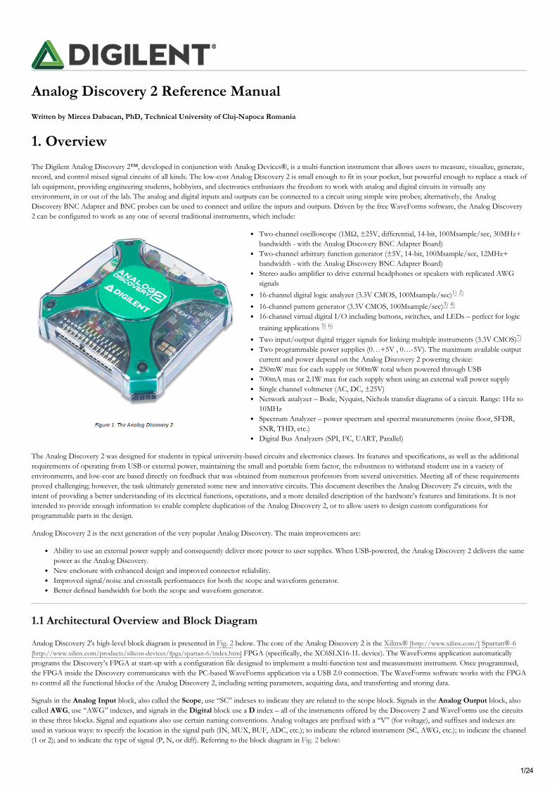
2.1. Scope Input Divider and Gain Selection
Figure 3 shows the scope input divider and gain selection stage.
Two symmetrical R-C dividers provide:
Scope input impedance = 1MOhm || 24pF
3/24
Two different attenuations for high-gain/low-gain (10:1)Controlled capacitance, much higher than the parasitical capacitance of subsequent stagesConstant attenuation and high CMMR over a large frequency range (trimmer adjusted)Protection for overvoltage (with the ESD diodes of the ADG612 inputs)
The maximum voltage rating for scope inputs is limited by C1 thru C24 to:
−50V < V inP, V inN < 50V
The maximum swing of the input signal to avoid signal distortion by opening the ADG612 ESD diodes is (for both low-gain and high-gain):
−26V < V inP, V inN < 26V
An analog switch (ADG612 [http://www.analog.com/en/switchesmultiplexers/analog-switches/adg612/products/product.html]) allows selecting high-gain versus low-gain(EN_HG_SC1, EN_LG_SC1) signals from the FPGA. The P and N branches of the differential path are switched together.
The ADG612 quad switch was used because it provides excellent impedance and bandwidth parameters:
1 pC charge injection±2.7 V to ±5.5 V dual-supply operation100 pA maximum at 25°C leakage currents85 Ω on resistanceRail-to-rail switching operationTypical power consumption: <0.1 μWTTL-/CMOS-compatible inputs-3 dB Bandwidth 680 MHz5 pF each of CS, CD (ON or OFF)
The low gain is:
VmuxV in
=R6
R1 + R4 + R6= 0.019
The low gain is used for input voltages:
|V indiff | = |V inP − V inN | < 50V
The high gain is:
VmuxV in
=R4 + R6
R1 + R4 + R6= 0.212
The high gain is used for input voltages:
|V indiff | = |V inP − V inN | < 7V
Figure 3. Input divider and gain selection.

4/24
2.2. Scope Buffer
A non-inverting OpAmp stage provides very high impedance as load for the input divider (Fig. 4).
Figure 4. Scope buffer.
The useful features of the AD8066 [http://www.analog.com/en/high-speed-op-amps/fet-input-amplifiers/ad8066/products/product.html] are:
FET input amplifier1 pA input bias currentLow costHigh speed: 145 MHz, −3 dB bandwidth (G = +1)180 V/μs slew rate (G = +2)Low noise 7 nV/√Hz (f = 10 kHz), 0.6 fA/√Hz (f = 10 kHz)Wide supply voltage range: 5 V to 24 VRail-to-rail outputLow offset voltage 1.5 mV maximumExcellent distortion specificationsSFDR −88 dBc @ 1 MHzLow power: 6.4 mA/amplifier typical supply currentSmall packaging: MSOP-8
Resistors and capacitors in the figure help to maximize the bandwidth and reduce peaking (which might be significant at unity gain).
The AD8066 [http://www.analog.com/en/high-speed-op-amps/fet-input-amplifiers/ad8066/products/product.html] is supplied ± 5.5V.
The maximum input voltage swing is: −5.5V < VmuxP, VmuxN < 2.2V
The maximum output voltage swing is: −5.38V < VbufP, VbufN < 5.4V
The gain is:
VbufVmux
= 1
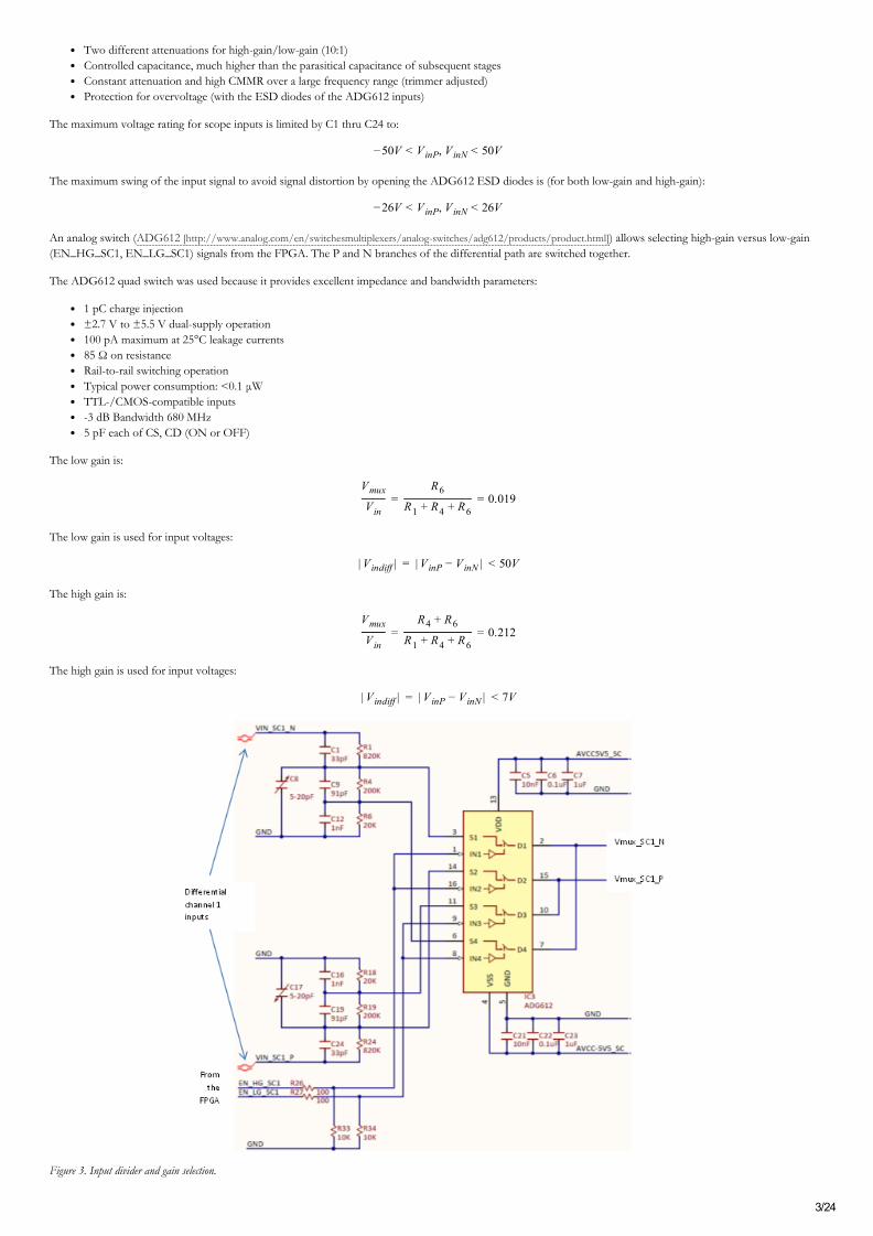
2.3. Scope Reference and Offset
Figure 5 shows the scope voltage reference sources and offset control stage. A low noise reference is used to generate reference voltages for all the scope stages.Buffered and scaled replicas of the reference voltages are provided for the buffer stages and individually for each scope channel to minimize crosstalk. A dual channelDAC generates the offset voltages, to be added over the input signal, for vertical position. Buffers are used to provide low impedance.
ADR3412ARJZ [http://www.analog.com/en/special-linear-functions/voltage-references/adr3412/products/product.html] – Micropower, high accuracy voltage reference:
Initial accuracy: ±0.1% (maximum)Low temperature coefficient: 8 ppm/°CLow quiescent current: 100 μA (maximum)Output noise (0.1 Hz to 10 Hz): <10 μV p-p at 1.2 V (typical)
AD5643 [http://www.analog.com/en/digital-to-analog-converters/da-converters/ad5643r/products/product.html] - Dual 14-Bit nanoDAC®:
Low power, smallest dual nanoDAC2.7 V to 5.5 V power supplySerial interface up to 50 MHz
ADA4051-2 [http://www.analog.com/en/all-operational-amplifiers-op-amps/operational-amplifiers-op-amps/ada4051-2/products/product.html] – Micropower, Zero-drift, Rail-to-rail input/output Op Amp:
5/24
Very low supply current: 13 μA typicalLow offset voltage: 15 μV maximumOffset voltage drift: 20 nV/°CHigh PSRR: 110 dB minimumRail-to-rail input/outputUnity-gain stable
The reference voltages generated for the scope stages are:
VrefSC = Vref1V2 ⋅ 1 +R79R80
= 2V
The offset voltages for the scope stages are:
0 ≤ VoffSC = VoutAD5643 ⋅ 1 +R77R78
< 4.044V
Figure 5. Scope reference and offset.
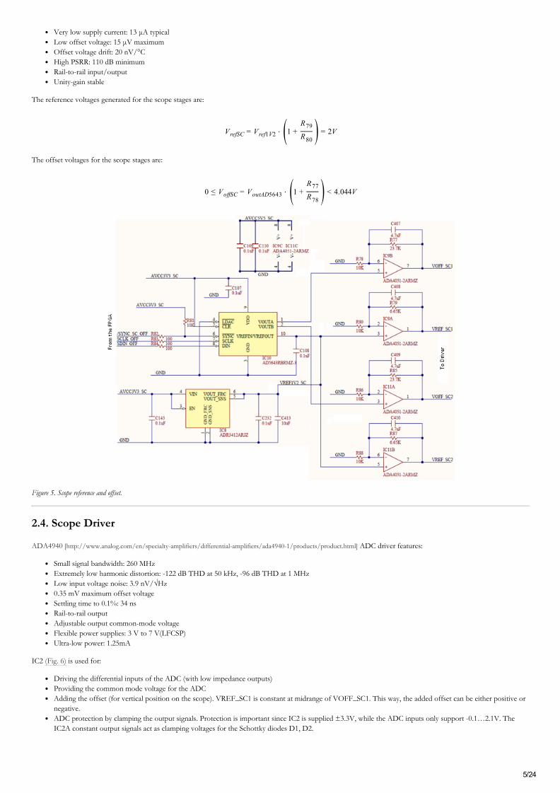
2.4. Scope Driver
ADA4940 [http://www.analog.com/en/specialty-amplifiers/differential-amplifiers/ada4940-1/products/product.html] ADC driver features:
Small signal bandwidth: 260 MHzExtremely low harmonic distortion: -122 dB THD at 50 kHz, -96 dB THD at 1 MHzLow input voltage noise: 3.9 nV/√Hz0.35 mV maximum offset voltageSettling time to 0.1%: 34 nsRail-to-rail outputAdjustable output common-mode voltageFlexible power supplies: 3 V to 7 V(LFCSP)Ultra-low power: 1.25mA
IC2 (Fig. 6) is used for:
Driving the differential inputs of the ADC (with low impedance outputs)Providing the common mode voltage for the ADCAdding the offset (for vertical position on the scope). VREF_SC1 is constant at midrange of VOFF_SC1. This way, the added offset can be either positive ornegative.ADC protection by clamping the output signals. Protection is important since IC2 is supplied ±3.3V, while the ADC inputs only support -0.1…2.1V. TheIC2A constant output signals act as clamping voltages for the Schottky diodes D1, D2.
( )
( )
6/24
Figure 6. Scope driver.
ADA4940 [http://www.analog.com/en/specialty-amplifiers/differential-amplifiers/ada4940-1/products/product.html] is supplied ±3.3V. The common mode voltage range is:
−3.5V < V +ADA4940 = V −ADA4940 < 2.1V
The signal gain is:
VADCdiffVbufdiff
=R9R8
=R17R16
= 1.77
The offset gain is:
VADCdiffVoffSC − VrefSC
=R9R3
=R17R22
= 1
The common mode gain is:
VCMVADCP + VADCN/ 2
= 1
The clamping voltages are:
VOut− IC2A = VCM −AVCC1V8
2 ⋅R23R25
= 0.9V −1.8V2 ⋅
4.99K6.34K = 0.2V
VOut+ IC2A = VCM −AVCC1V8
2 ⋅R23R25
= 0.9V +1.8V2 ⋅
4.99K6.34K = 1.6V
D1, D2 clamp the VADC signals to the protected levels of:
−0.1V < V +ADA4940 = V −ADA4940 < 1.9V
2.5. Clock Generator
A precision oscillator (IC31) generates a low jitter, 20 MHz clock (see Fig. 8).
The ADF4360-9 Clock Generator PLL with Integrated VCO is configured for generating a 200 MHz differential clock for the ADC and a 100 MHz single-endedclock for the DAC.
Analog Devices ADIsimPLL software was used for designing the clock generator (see Fig. 7). The PLL filter is optimized for constant frequency (low Loop

7/24
Bandwidth = 50 kHz and Phase Margin = 60°). Simulation results are shown below. The Phase jitter using a brick wall filter (10.0 kHz to 100 kHz) is 0.04° rms.
Figure 7. Phase noise figure for the clock generator.
Figure 8. Clock generator.
2.6. Scope ADC
2.6.1. Analog Section
The Analog Discovery 2 uses a dual channel, high speed, low power, 14-bit, 105MSPS ADC (Analog part number AD9648 [http://www.analog.com/en/analog-to-digital-converters/ad-converters/ad9648/products/product.html]), as shown in Fig. 9 .

8/24
Figure 9. ADC - analog section.
The important features of AD9648:
SNR = 74.5dBFS @70 MHzSFDR =91dBc @70 MHzLow power: 78mW/channel ADC core@ 125MSPSDifferential analog input with 650 MHz bandwidthIF sampling frequencies to 200 MHzOn-chip voltage reference and sample-and-hold circuit2 V p-p differential analog inputDNL = ±0.35 LSBSerial port control optionsOffset binary, gray code, or two's complement data formatOptional clock duty cycle stabilizerInteger 1-to-8 input clock dividerData output multiplex optionBuilt-in selectable digital test pattern generationEnergy-saving power-down modesData clock out with programmable clock and data alignment
The differential inputs are driven via a low-pass filter comprised of C141 together with R10 through R13, in the buffer stage. The differential clock is AC-coupled andthe line is impedance matched. The clock is internally divided by two for operating at a constant 100 MHz sampling rate. An external reference voltage is used,buffered by IC 19. The ADC generates the common mode reference voltage (VCM_SC) to be used in the buffer stage.
The differential input voltage range is:
−1V < VADC diff < 1V
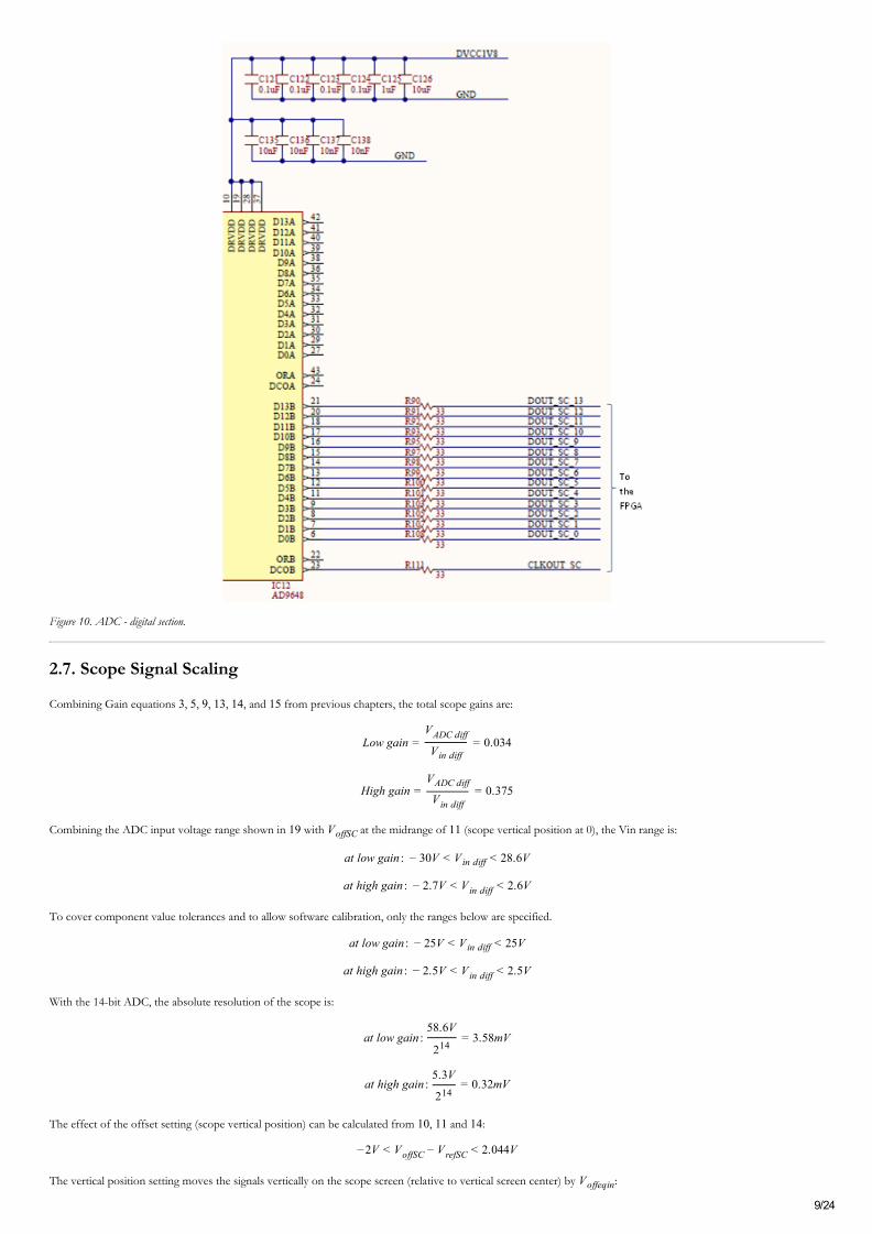
2.6.2. Digital Section
The digital stage of the ADC and the corresponding FPGA bank are supplied at 1.8V.
To minimize the number of used FPGA pins; a multiplexed mode is used, to combine the two channels on a single data bus. CLKOUT_SC is provided to the FPGAfor synchronizing data (see Fig. 10).
9/24
Figure 10. ADC - digital section.
2.7. Scope Signal Scaling
Combining Gain equations 3, 5, 9, 13, 14, and 15 from previous chapters, the total scope gains are:
Low gain =VADC diffV in diff
= 0.034
High gain =VADC diffV in diff
= 0.375
Combining the ADC input voltage range shown in 19 with VoffSC at the midrange of 11 (scope vertical position at 0), the Vin range is:
at low gain : − 30V < V in diff < 28.6V
at high gain : − 2.7V < V in diff < 2.6V
To cover component value tolerances and to allow software calibration, only the ranges below are specified.
at low gain : − 25V < V in diff < 25V
at high gain : − 2.5V < V in diff < 2.5V
With the 14-bit ADC, the absolute resolution of the scope is:
at low gain :58.6V
214= 3.58mV
at high gain :5.3V
214= 0.32mV
The effect of the offset setting (scope vertical position) can be calculated from 10, 11 and 14:
−2V < VoffSC − VrefSC < 2.044V
The vertical position setting moves the signals vertically on the scope screen (relative to vertical screen center) by Voffeqin:
10/24
at low gain : − 59.3V < Voff eq in < 59.3V
at high gain : − 5.39V < Voff eq in < 5.39V
The above adds an equivalent offset voltage Voffeqin to V indiff, translating the ranges in 21 and 22 by Voffeqin , up to the limits in 25.
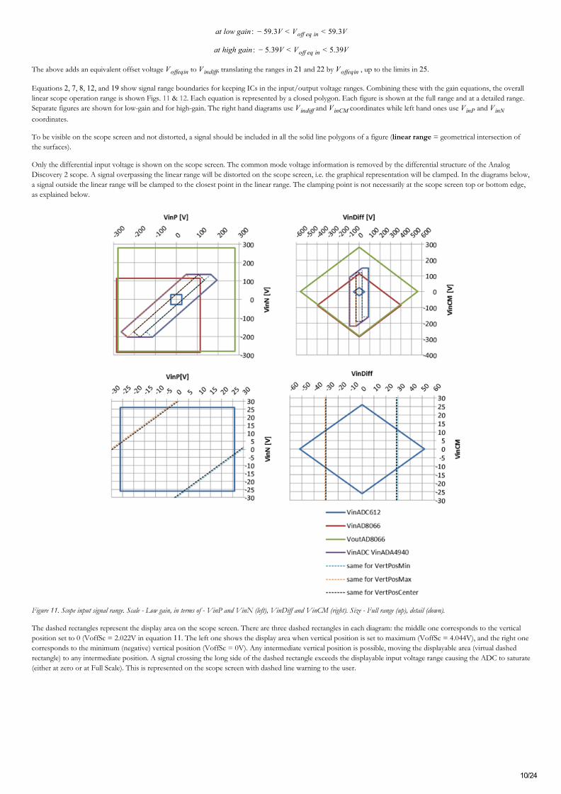
Equations 2, 7, 8, 12, and 19 show signal range boundaries for keeping ICs in the input/output voltage ranges. Combining these with the gain equations, the overalllinear scope operation range is shown Figs. 11 & 12. Each equation is represented by a closed polygon. Each figure is shown at the full range and at a detailed range.Separate figures are shown for low-gain and for high-gain. The right hand diagrams use V indiff and V inCM coordinates while left hand ones use V inP and V inNcoordinates.
To be visible on the scope screen and not distorted, a signal should be included in all the solid line polygons of a figure (linear range = geometrical intersection ofthe surfaces).
Only the differential input voltage is shown on the scope screen. The common mode voltage information is removed by the differential structure of the AnalogDiscovery 2 scope. A signal overpassing the linear range will be distorted on the scope screen, i.e. the graphical representation will be clamped. In the diagrams below,a signal outside the linear range will be clamped to the closest point in the linear range. The clamping point is not necessarily at the scope screen top or bottom edge,as explained below.
Figure 11. Scope input signal range. Scale - Low gain, in terms of - VinP and VinN (left), VinDiff and VinCM (right). Size - Full range (up), detail (down).
The dashed rectangles represent the display area on the scope screen. There are three dashed rectangles in each diagram: the middle one corresponds to the verticalposition set to 0 (VoffSc = 2.022V in equation 11. The left one shows the display area when vertical position is set to maximum (VoffSc = 4.044V), and the right onecorresponds to the minimum (negative) vertical position (VoffSc = 0V). Any intermediate vertical position is possible, moving the displayable area (virtual dashedrectangle) to any intermediate position. A signal crossing the long side of the dashed rectangle exceeds the displayable input voltage range causing the ADC to saturate(either at zero or at Full Scale). This is represented on the scope screen with dashed line warning to the user.

11/24
Figure 12. Scope input signal range. Scale - High gain, in terms of - VinP and VinN (left), VinDiff and VinCM (right). Size - Full range (up), detail (down).
A signal keeping within the dashed rectangle but crossing any solid line overrides electrical limits of intermediate circuits in the signal path (see the legend of thefigures). This results in distorting the signal without saturating the ADC. The software has no information about this situation and cannot warn the user with specificsignal representation. It is the user’s responsibility to understand and avoid such situations.
For low gain (Fig. 11), the simple condition to stay in the linear range is to keep both positive and negative inputs V inP, V inN in the ±26V range (as shown byequation 2).
For high gain (Fig. 12), by combining equations 7 and 5, both positive and negative inputs in must stay in the range:
−26V < V inP, V inN < 10V
Additionally, the differential input signal (combined with the equivalent offset voltage – vertical position) is visible only within the range:
−7.5V < V inDiff < 7.5V
Note the difference between typical parameter values considered by the figures and the safer min/max values used for the equations.
Figure 13 shows an example of a signal distorted due to a common mode input voltage that is too large. The grey line is the reference, not distorted, signal. Thedifferential input voltage is a 4Vpp triangle on top of a -5V DC component. The common mode input voltage is 10V. The vertical position of the scope is set to 5Vand high gain is selected. The yellow line shows an identical signal, except the common mode input voltage is 15V.
Figure 13. Common mode input voltage limitation.
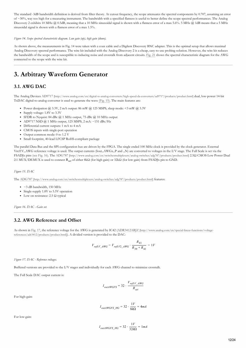
2.8 Scope Spectral Characteristics
Figure 14 shows a typical spectral characteristic of the scope. An Agilent 3320A 20 MHz Function/Arbitrary Waveform Generator was used to generate the inputsignal of 1VRMS. The signal swept from 100 Hz to 30 MHz. A coax cable and a Digilent Discovery BNC adapter were used to connect the input signal to theDiscovery inputs.
The Network Analyzer was used, the WaveGen was set to External, the Gain was set at x10 (high-gain) for the upper figure, and x0.1 (low-gain) for the lower one.For both scales, the 3dB bandwidth is 30 MHz+. The 0.5dB bandwidth is 10 MHz and the 0.1dB bandwidth is 5 MHz.
12/24
The standard -3dB bandwidth definition is derived from filter theory. At cutout frequency, the scope attenuates the spectral components by 0.707, assuming an errorof ~30%, way too high for a measuring instrument. The bandwidth with a specified flatness is useful to better define the scope spectral performances. The AnalogDiscovery 2 exhibits 10 MHz @ 0.5dB, meaning that a 10 MHz sinusoidal signal is shown with a flatness error of a max 5.6%. 5 MHz @ 1dB means that a 5 MHzsinusoidal signal is shown with a flatness error of a max 1.5%.
Figure 14. Scope spectral characteristic diagram. Low gain (up), high gain (down).
As shown above, the measurements in Fig. 14 were taken with a coax cable and a Digilent Discovery BNC adapter. This is the optimal setup that allows maximalAnalog Discovery spectral performance. The wire kit included with the Analog Discovery 2 is a cheap, easy-to-use probing solution. However, the wire kit reducesthe bandwidth of the scope and is susceptible to inducing noise and crosstalk from adjacent circuits. Fig. 21 shows the spectral characteristic diagram for the AWGconnected to the scope with the wire kit.
3. Arbitrary Waveform Generator
3.1. AWG DAC
The Analog Devices AD9717 [http://www.analog.com/en/digital-to-analog-converters/high-speed-da-converters/ad9717/products/product.html] dual, low-power 14-bitTxDAC digital-to-analog converter is used to generate the wave (Fig. 15). The main features are:
Power dissipation @ 3.3V, 2 mA output: 86 mW @ 125 MSPS, sleep mode: <3 mW @ 3.3VSupply voltage: 1.8V to 3.3VSFDR to Nyquist: 84 dBc @ 1 MHz output, 75 dBc @ 10 MHz outputAD9717 NSD @ 1 MHz output, 125 MSPS, 2 mA: −151 dBc/HzDifferential current outputs: 1 mA to 4 mACMOS inputs with single-port operationOutput common mode: 0 to 1.2 VSmall footprint, 40-lead LFCSP RoHS-compliant package
The parallel Data Bus and the SPI configuration bus are driven by the FPGA. The single ended 100 MHz clock is provided by the clock generator. ExternalVref1V_AWG reference voltage is used. The output currents (Iout_AWGx_P and _N) are converted to voltages in the I/V stage. The Full Scale is set via theFSADJx pins (see Fig. 16). The ADG787 [http://www.analog.com/en/switchesmultiplexers/analog-switches/adg787/products/product.html] 2.5Ω CMOS Low Power Dual2:1 MUX/DEMUX is used to connect Rset of either 8kΩ (for high gain) or 32kΩ (for low gain) from FSADJx pin to GND.
Figure 15. DAC
The ADG787 [http://www.analog.com/en/switchesmultiplexers/analog-switches/adg787/products/product.html] features:
−3 dB bandwidth, 150 MHzSingle-supply 1.8V to 5.5V operationLow on resistance: 2.5 Ω typical
Figure 16. DAC - Gain set.
3.2. AWG Reference and Offset
As shown in Fig. 17, the reference voltage for the AWG is generated by IC42 (ADR3412ARJZ [http://www.analog.com/en/special-linear-functions/voltage-references/adr3412/products/product.html]). A divided version is provided to the DAC:
Vref1V_AWG = Vref1V2_AWG ⋅R41
R39 + R41= 1V
Figure 17. DAC - Reference voltages.
Buffered versions are provided to the I/V stages and individually for each AWG channel to minimize crosstalk.
The Full Scale DAC output current is:
IoutAWGFS = 32 ⋅Vref1V_AWG
Rset
For high-gain:
IoutAWGFS_HG = 32 ⋅1V8kΩ
= 4mA
For low-gain:
IoutAWGFS_HG = 32 ⋅1V32kΩ
= 1mA

13/24
An AD5645R [http://www.analog.com/en/digital-to-analog-converters/da-converters/ad5645r/products/product.html] Quad 14-bit nanoDAC generates the offset voltagesto add a DC component to the AWG output signal (Fig. 18). The same circuit also generates VSET+ USR and VSET- USR, used to set the +/- user supply voltages.
Low power, smallest quad 14-bit nanoDAC2.7 V to 5.5 V power supplyMonotonic by designPower-on reset to zero scale/midscale (important for starting the AWG with 0 DC component)
Figure 18. DAC - Offset voltages and user PS setting.
The Full Scale voltage of all IC43 outputs is:
VoffAWGFS = VSET_USRFS = Vref1V2AWG = 1.2V
3.3. AWG I/V
IC 15 in Fig. 19 converts the DAC output currents to a bipolar voltage.
Important AD8058 [http://www.analog.com/en/all-operational-amplifiers-op-amps/operational-amplifiers-op-amps/ad8058/products/product.html] features:
Low cost325 MHz, −3 dB bandwidth (G = +1)1000 V/μs slew rateGain flatness: 0.1 dB to 28 MHzLow noise: 7 nV/√HzLow power: 5.4 mA/amplifier typical @ 5 VLow distortion: −85 dBc@5MHz, RL=1kΩWide supply range from 3 V to 12 VSmall packaging
VAudio = IoutAWGP ⋅ R148 − IoutAWGN ⋅ R142 =
= (1 − 2 ⋅ AU) ⋅ IoutAWGFS ⋅ R142 = Ab ⋅ IoutAWGFS ⋅ R142
Where:
AU =D
2N∈ [0…1); − normalized unipolar DAC input number
AB = 1 − 2 ⋅ AU ∈ [−1…1); − normalized bipolar DAC input number (binary offset)
D ∈ 0…214 = 0…214 − 1 ; − integer unipolar DAC input number
The Voltage range extends between:
−VAudioFS ≤ VAudio < − VAudioFS
Where (for high gain, respectively, low gain):
VAudioFS HG = IoutAWGFS HG ⋅ R142 = 496mV
VAudioFS LG = IoutAWGFS LG ⋅ R142 = 124mV
Figure 19. AWG I/V and out.
3.4. AWG Out
IC16 in Fig. 19 is the output stage of the AWG. AD8067 [http://www.analog.com/en/all-operational-amplifiers-op-amps/operational-amplifiers-op-amps/ad8067/products/product.html] features:
FET input: 0.6 pA input bias currentStable for gains ≥8 for High-Capacitive LoadHigh speed: 54 MHz@−3 dB (G = +10)640 V/µs slew rateLow noise:6.6 nV/√Hz; 0.6 fA/√HzLow offset voltage (1.0 mV max)Rail-to-rail outputLow distortion: SFDR 95 dBc @ 1 MHzLow power: 6.5 mA typical supply currentLow cost; Small packaging: SOT-23-5
( )
[ ) [ ]

14/24
Matching the impedances in the inverting and non-inverting inputs of IC16:
1R140
+1
R141+
1R144
=1
R147+
1R149
VoutAWG = − VAudio ⋅R141R144
+ 2 ⋅ VoffAWG − Vref1V2AWG ⋅R141R140
The first term in equation 38 represents the actual wave amplitude, with a range of:
−5.45V < − 5V < VACoutAWG HG < 5V < 5.45V
−1.36V < 1.25V < VACoutAWG LG < 1.25V < 1.36V
Low-gain is used to generate low amplitude signals with improved accuracy. Any amplitude of the output signal is derivable by combining LowGain/HighGain setting(rough) with the digital signal amplitude (fine).
With the 14-bit DAC, the absolute resolution of the AWG AC component is:
at Low Gain :2.72V
214= 166μV
at High Gain :10.9V
214= 665μV
The second term in equation 38 shows the DC component (AWG offset), with a range of (for either LowGain or HighGain):
−5.5V < 5V < VDCoutAWG < 5V < 5.5V
AD8067 is supplied with ±5.5V; to avoid saturation the user should keep the sum of AC and DC components in 38 to:
−5.5V < 5V < VoutAWG < 5V < 5.5V
Only bolded ranges are used in equations 39, 41, and 42, for providing tolerance margins.
The R145 PTC thermistor provides thermal protection in case of an output shortcut.
3.5. Audio
A stereo audio output combines the two AWG channels (Fig. 20). AD8592 [http://www.analog.com/en/audiovideo-products/audio-amplifiers/ad8592/products/product.html] was used for its features:
Single-supply operation: 2.5 V to 6 VHigh output current: ±250 mALow shutdown supply current: 100 nALow supply current: 750 μA/AmpVery low input bias current
A single 3.3V supply is used.
VoutIC18 = − 2 ⋅ VAudio + 1.5V
The first term in equation 43 is the audio signal. The second term is the common mode DC component, removed by AC coupling.
The audio signal range is:
VAudioJack = − 2 ⋅ VAudio
−992mV < VAudioJack < 992mV(High Gain)
−248mV < VAudioJack < 248mV(Low Gain)
Figure 20. Audio.
3.6. AWG Spectral Characteristics
Figure 21 shows the typical spectral characteristic of the AWG. In the first experiment (up), a coax cable and a Digilent Discovery BNC adapter were used to connectthe AWG signal to the Scope inputs. For the second experiment (down), the AWG was connected to the scope inputs via the Analog Discovery wire kit. The AnalogDiscovery 2 Scope hardware was considered a reference for the experiments above because it has preferred spectral characteristics to the AWG.
The Network Analyzer virtual instrument in WaveForms is used to perform synchronized signal synthesis and acquisition. It takes control of channel 1 of AWG andof both scope channels. Start/Stop frequencies are set to 100 Hz/25 MHz, respectively. Sinus amplitude is set to 1V. The characteristic is built in 100 steps. The 3dBbandwidth is 12 MHz with the coax cable and 9 MHz with the wire kit. The 0.5dB bandwidth is 4 MHz with the coax cable and 2.9 MHz with the wire kit. The 0.1dBis 1 MHz with the coax cable and 800 kHz with the wire kit.
( )
15/24
Figure 21. AWG spectral characteristics. With Analog Discovery BNC Adapter and BNC cable from AWG to Scope (up). With the wire kit (down).
4. Calibration MemoryThe analog circuitry described in previous chapters includes passive and active electronic components. The datasheet specs show parameters (resistance, capacitance,offsets, bias currents, etc.) as typical values and tolerances. The equations in previous chapters consider typical values. Component tolerances affect DC, AC, andCMMR performances of the Analog Discovery 2. To minimize these effects, the design uses:
0.1% resistors and 1% capacitors in all the critical analog signal pathsCapacitive trimmers for balancing the Scope Input Divider and Gain SelectionNo other mechanical trimmers (as these are big, expensive, unreliable and affected by vibrations, aging, and temperature drifts)Software calibration, at manufacturingUser software calibration, as an option
A software calibration is performed on each device as a part of the manufacturing test. AWG signals are passed to a reference instrument and reference signals areconnected to the Scope inputs. A set of measurements is used to identify all the DC errors (Gain, Offset) of each analog stage. Correction (Calibration) parametersare computed and stored in the Calibration Memory, on the Analog Discovery 2 device, as Factory Calibration. The WaveForms software allows the user performingan in-house calibration and overwrite the Calibration Data. Returning to Factory Calibration is always possible.
The WaveForms Software reads the calibration parameters from the connected Analog Discovery 2 and uses them to correct both generated and acquired signals.
5. Digital I/OFigure 22 shows half of the Digital I/O pin circuitry (the other half is symmetrical). J3 is the Analog Discovery 2 user signal connector.
General purpose FPGA I/O pins are used for Analog Discovery 2 Digital I/O. FPGA pins are set to SLOW slew rate and 4mA drive strength, with no internal pull.
PTC thermistors provide thermal protection in case of shortcuts. Schottky Diodes double the internal FPGA ESD protection diodes for increasing the acceptablecurrent in case of overvoltage. Nominal resistance of the PTCs (220Ω) and parasitical capacitance of the Schottky diodes (2.2pF) and FPGA pins (10pF) limit thebandwidth of the input pins. For output pins, the PTCs and the load impedance limit the bandwidth and power.
Input and output pins are LVCMOS3V3. Inputs are 5V tolerant. Overvoltage up to ±20V is supported.
Figure 22. Digital I/O.
6. Power Supplies and ControlThis block includes all power monitoring and control circuitry, internal power supplies, and user power supplies.
6.1. USB Power Control
As shown in Fig. 23, the Analog Discovery 2's power can be supplied either from the USB port (VBUS) or from an external power supply (J4 connector).
Figure 23. USB power control.
The external power input is protected against reverse voltage; Q4 turns OFF if a floating power supply with negative polarity on central pin of J4 is used. However,the device is not protected for a very unlikely use case:
Analog Discovery 2 connected to the USB port of a PC which has GND connected to EARTHExternal power supply with negative polarity on central pin of J4 and with exterior pin connected to EARTH.
In this case, the external EARTH loop acts as a shortcut of Q4.
ADCMP671 [http://www.analog.com/en/products/linear-products/comparators/adcmp671.html] is a window comparator with the following features:
Window monitoring with minimum processor I/OIndividually monitoring N rails with only N + 1 processor I/O400 mV ± 0.275% threshold at VDD = 3.3 V, 25°CSupply range: 1.7 V to 5.5 VLow quiescent current: 8.55 μA maximumInput range includes groundInternal hysteresis: 9.2 mV typicalLow input bias current: ±2.5 nA maximumOpen-drain outputsPower good indication outputDesignated over voltage indication outputLow profile (1 mm), 6-lead TSOT package

16/24
IC48 drives PWRGD output HIGH (turning IC26 ON) when Vext is in the range:
4.11V = 400mV ⋅R248 + R249 + R273
R249 + R273< Vext < 400mV ⋅
R248 + R249 + R273R273
= 5.76V
The Analog Discovery 2 exhibits two main powering modes: USB and External. Temporary modes (Racing OFF, USB OFF and Racing) are explained here fordesign clarifications, but have no importance for the user observed behavior.
Racing OFF – immediately after reset, before FPGA is programmed, if an external power supply is attached and in the right range (PWRGD = HIGH).USB OFF – immediately after reset, before FPGA is programmed, if external power supply is missing or out-of-range (PWRGD = LOW).USB – all the power is drained from the Vbus (IC21 = ON, IC26 = OFF). The external power supply is either missing or out of the right voltage range. Thepower available for both User Supplies is limited to 0.7W.Racing – when external power supply is in the right voltage range (PWRGD = HIGH), before WaveForms stops the USB Power Controller. During racingmode, both USB Power Controller (IC21) and External Power controller (IC26) are ON, the device drains power from whatever supply has a higher voltage(D28 and D29 work as a maxim voltage detector). The Racing mode is temporary, it ends when the FPGA is configured and communicates with theWaveForms software. During Racing mode, the power available for User Supplies is limited.External – the device is powered from an external supply (via the 5V DC connector and IC26). Vext is in the range shown by equation 45 (PWRGD =HIGH, and WaveForms already stopped the USB Power Controller (IC21). The User Supplies current and power limits are increased to 700mA or 2.1W each.The only circuit still supplied from the USB VBUS is the USB controller (IC41).
At Power ON, the FPGA is not programmed, EN_VBUS is HiZ, the pulldown resistor R246 turns Q1 OFF, IC21 is ON via R174. The Analog Discovery 2 starts inUSB OFF mode (when PWRGD = LOW) or Racing OFF mode (when PWRGD = HIGH). The WaveForms software first configures the FPGA, and the deviceturns into USB or Racing mode, depending on presence/absence of correct external supply voltage. The FPGA continuously monitors the voltage at the 5V DCconnector. When detecting the Racing mode (PWRGD = HIGH), WaveForms sends the command to drive EN_VBUS HIGH, turning the USB Power Controller(IC21) OFF, thus switching to External mode.
If external Power Supply is attached after WaveForms started and runs several instruments, the device steps seamlessly trough USB → Racing → External modes.Running instruments are not affected, except User Supplies get more available power.
However, removing the external power supply during External mode is not seamless. Only the USB controller keeps working (as supplied from the USB port). TheFPGA gets unpowered and loses configuration data. The device stops all the instruments, EN_VBUS go HiZ, which leads to the USB OFF mode. WaveForms willprompt the user to select the device, which will re-program the FPGA. All the instruments can then be run, in the USB mode.
An ADM1177 [http://www.analog.com/en/power-management/power-monitors/adm1177/products/product.html] Hot Swap Controller and Digital Power Monitor withSoft Start Pin is used to provide USB power compliance during USB and Racing modes (IC21 in Fig. 23).
Remarkable ADM1177 features are:
Safe live board insertion and removalSupply voltages from 3.15 V to 16.5 VPrecision current sense amplifier12-bit ADC for current and voltage readAdjustable analog current limit with circuit breaker±3% accurate hot swap current limit levelFast response limits peak fault currentAutomatic retry or latch-off on current faultProgrammable hot swap timing via TIMER pinSoft start pin for reference adjustment and programming of initial current ramp rateI2C fast mode-compliant interface (400 kHz maximum)
When enabled, (in USB or Racing modes), IC21 limits the current consumed from the USB port to:
I limit =100mVR173
=100mV0.1Ω = 1A
For a maximum time of:
tfault = 21.7[ms/μF] ⋅ C80 = 21.7[ms/μF] ⋅ 0.47μF = 10.2ms
If the consumed current does not fall below I limit before tfault, IC21 turns off Q2A. A hot swap retry is initiated after:
tcool = 550[ms/μF] ⋅ C80 = 550msμF ⋅ 0.47μF = 258.5ms
To avoid high inrush currents at hot swap, Soft Start circuitry limits the current slope to:
dI limitdt =
10μAC81
⋅1
10 ⋅ R173= 212
mAms
If the current drops below I limit before tfault, normal operation begins.
Similarly, IC26 (in Racing or External modes), limits the current consumed from the external power supply to:
I limit =100mVR247
=100mV0.036Ω = 2.78A
[ ]
17/24
tfault and tcool are same as for IC21, and the current slope limit is:
dI limitdt =
10μAC432
⋅1
10 ⋅ R247= 591
mAms
The Analog Discovery 2 user pins are overvoltage protected. Overvoltage (or ESD) diodes short when a user pin is overdriven by the external circuitry (Circuit UnderTest), back powering the input/output block and all the circuits sharing the same internal power supply. If the back-powered energy is higher than the used energy,the bi-directional power supply recovers the difference and delivers it to the previous node in the power chain. Eventually, the back-powering energy could arrive tothe USB VBUS, raising the voltage above the 5V nominal value. D28 in Fig. 23 protects the PC USB port against such a situation.
6.2. Analog Supplies Control
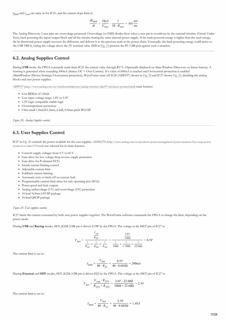
During USB mode, the FPGA constantly reads from IC21 the current value through R173. (Optionally displayed on Main Window/Discovery or Status button). Awarning is generated when exceeding 500mA (Status: OC = Over Current). If a value of 600mA is reached and Overcurrent protection is enabled(MainWindow/Device/Settings/Overcurrent protection), WaveForms turns off IC20 (ADP197) shown in Fig. 24 and IC27 shown Fig. 25, disabling the analogblocks and user power supplies.
ADP197 [http://www.analog.com/en/switchesmultiplexers/analog-switches/adp197/products/product.html] main features:
Low RDSon of 12mΩLow input voltage range: 1.8V to 5.5V1.2V logic compatible enable logicOvertemperature protectionUltra-small 1.0mmX1.5mm, 6 ball, 0.5mm pitch WLCSP
Figure 24. Analog Supplies control.
6.3. User Supplies Control
IC27 in Fig. 25 controls the power available for the user supplies. ADM1270 [http://www.analog.com/en/products/power-management/power-monitors/hot-swap-power-monitors-ic/adm1270.html] was selected for its main features:
Controls supply voltages from 4 V to 60 VGate drive for low voltage drop reverse supply protectionGate drive for P-channel FETsInrush current limiting controlAdjustable current limitFoldback current limitingAutomatic retry or latch-off on current faultProgrammable current-limit timer for safe operating area (SOA)Power-good and fault outputsAnalog undervoltage (UV) and overvoltage (OV) protection16-lead 3x3mm LFCSP package16-lead QSOP package
Figure 25. User supplies control.
IC27 limits the current consumed by both user power supplies together. The WaveForms software commands the FPGA to change the limit, depending on thepower mode.
During USB and Racing modes, SET_ILIM_USR pin is driven LOW by the FPGA. The voltage at the ISET pin of IC27 is:
V Iset =
VcapR253
1R253
+1R254
+1R255
=
3.6V
10kΩ1
10kΩ+
11.74kΩ
+1
22.6kΩ
= 0.5V
The current limit is set to:
I limit =V Iset
40 ⋅ R21=
0.5V40 ⋅ 0.043Ω
= 290mA
During External and OFF modes, SET_ILIM_USR pin is driven HiZ by the FPGA. The voltage at the ISET pin of IC27 is:
V Iset =Vcap ⋅ R255R253 + R255
=3.6V ⋅ 22.6kΩ10kΩ + 22.6kΩ
= 2.5V
The current limit is set to:
I limit =V Iset
40 ⋅ R21=
2.5V40 ⋅ 0.043Ω
= 1.45A
18/24
In both cases, I limit is allowed for a maximum time of:
tfault = 21.7[ms/μF] ⋅ C170 = 21.7[ms/μF] ⋅ 4.7μF = 102ms
If the consumed current does not fall below I limit before tfault, IC21 turns off Q2. A hot swap retry is initiated after:
tcool = 550[ms/μF] ⋅ C80 = 550[ms/μF] ⋅ 4.7μF = 2.585s
Soft Start is not used; C183 is a No Load.
If the current drops below I limit before tfault, normal operation begins.
The current limited by equations 53 and 55 is shared by both positive and negative user power supplies. After considering the efficiency of the user supply stages,about 100mA is available for user in both supplies together, in USB Only mode. In External mode, the current/power limit for user is set in the User VoltageSupplies, as explained below.
6.4. User Voltage Supplies
The user power supplies (Fig. 26) use ADP1612 Switching Converter in Buck-Boost DC-to-DC topology. Main features:
1.4A current limitMinimum input voltage 1.8VPin-selectable 650 kHz or 1.3 MHz PWM frequencyAdjustable output voltage up to 20 VAdjustable soft startUndervoltage lockout
IC46A/B op amps insert the command voltages VSET+_USR and VSET−_USR, respectively, in the feedback loop. Additionally, IC46B introduces the requiredinversion for the negative supply.
Figure 26. User power supplies.
Since the op amps are included in negative feedback loops, the input pins voltages are equal:
V + IC46A =
VOUT+_USRR188
+VSET+_USRR193
1R188
+1R193
= V − IC46A =
VFBR266
1R265
+1R266
V + IC46B =
VOUT−_USRR187
+VFBR270
1R187
+1R270
= V − IC46B =
VSET−_USRR190
1R72
+1R190
The input impedances for the op amps are matched:
1R188
+1
R193=
1R265
+1
R266
1R187
+1
R270=
1R72
+1
R190
The user voltages are:
VOUT +_USR = VFB ⋅R188R266
− VSET +_USR ⋅R188R193
= 5.33V − 4.87 ⋅ VSET +_USR
VOUT −_USR = − VFB ⋅R187R270
+ VSET −_USR ⋅R187R190
= − 5.33V + 4.87 ⋅ VSET −_USR
Where:
VFB = 1.235V typical
IC43 (Fig. 18) generates the setting voltages in the range:
0 < VSET+_USR, VSET−_USR < 1.2V
Which would allow output voltages to be set in the ranges:
−0.51V ≤ VSET+_USR < 5.33V
0.51V ≥ VSET−_USR > − 5.33V
The margins allow for compensating the components’ tolerances. After calibration, the WaveForms SW only allows the ranges 0 to +/-5V respectively. Even so,

19/24
output voltages below absolute value of 0.5V are not guaranteed. With light loads, such voltages might exhibit significant ripple (~15mV).
Each supply can be disabled by the FPGA.
6.5. Internal Power Supplies
6.5.1. Analog Supplies
Analog supplies need to have very low ripple to prevent noise from coupling into analog signals. Ferrite beads are used to filter the remaining switching noise and toseparate the power supplies that go to the main analog circuit blocks, to avoid crosstalk.
The 3.3V (Fig. 27) and 1.8V Fig. 28 analog power supplies are implemented around an ADP2138 [http://www.analog.com/en/power-management/switching-regulators-integrated-fet-switches/adp2138/products/product.html] Fixed Output Voltage, 800mA, 3MHz, Step-Down DC-to-DC converter. To insure low output voltage ripple asecond LC filter is added and forced PWM mode is selected.
Input voltage: 2.3 V to 5.5 VPeak efficiency: 95%3 MHz fixed frequency operationTypical quiescent current: 24 μAVery small solution size6-lead, 1 mm × 1.5 mm WLCSP packageFast load and line transient response100% duty cycle low dropout modeInternal synchronous rectifier, compensation, and soft startCurrent overload and thermal shutdown protectionsUltra-low shutdown current: 0.2 μA (typical)Forced PWM and automatic PWM/PSM modes
Figure 27. 3.3V internal analog power supply.
Figure 28. 1.8V internal analog power supply.
The -3.3V analog power supply (Fig. 29) is implemented with the ADP2301 [http://www.analog.com/en/power-management/switching-regulators-integrated-fet-switches/adp2301/products/product.html] Step-Down regulator in an inverting Buck-Boost configuration. See application Note AN-1083: Designing an Inverting BuckBoost Using the ADP2300 and ADP2301 [http://www.analog.com/static/imported-files/application_notes/AN-1083.pdf]. The ADP2301 features:
1.2 A maximum load current±2% output accuracy over temperature range1.4 MHz switching frequencyHigh efficiency up to 91%Current-mode control architectureOutput voltage from 0.8 V to 0.85 × VINAutomatic PFM/PWM mode switchingIntegrated high-side MOSFET and bootstrap diode,Internal compensation and soft startUndervoltage lockout (UVLO), Overcurrent protection (OCP) and thermal shutdown (TSD)Available in ultrasmall, 6-lead TSOT package
Figure 29. -3.3V internal analog power supply.
The Output voltage is set with an external resistor divider from Vout to FB:
R180R181
=−Vout − Vref
Vref
Choosing R181 = 10.2k\Omega :
R180 =3.3V − 0.8V
0.8V⋅ 10.2kΩ = 31.87kΩ
Closest standard value is R180 = 31.6k\Omega
The 5.5V and -5.5V supplies Fig. 30 are created with a Sepic-Cuk topology, built around a single ADP1612 [http://www.analog.com/en/power-management/switching-regulators-integrated-fet-switches/adp1612/products/product.html] Step-Up DC-to DC converter. Both Sepic and Cuk converters are connected to the same switching pinof the regulator. Only the positive Sepic output is regulated, while the negative output tracks the positive one. This is an accepted behavior, since similar load currentsare expected on both positive and negative rails.
Figure 30. ±5.5V internal analog supplies.
The output current in a Sepic is discontinuous which results in a higher output ripple. To lower this ripple an additional output filter is added to the positive rail.
For more information see application note: AN-1106: An Improved Topology for Creating Split Rails from a Single Input Voltage
20/24
[http://www.analog.com/static/imported-files/application_notes/AN-1106.pdf].
Setting the Output Voltage:
R184R185
=Vout − Vref
Vref
Choosing R185 = 13.7kΩ:
R184 =5.5V − 1.235V
1.235V ⋅ 13.7kΩ = 47.31kΩ
Closest standard value is R184 = 47.5kΩ
6.5.2. Digital Supplies
The 1V digital supply (Fig. 31) is implemented with the ADP2120-1 [http://www.analog.com/en/power-management/switching-regulators-integrated-fet-switches/adp2120/products/product.html]. It has a fixed 1V output voltage option and a ±1.5% output accuracy which makes it suitable for the FPGA internal powersupply. It also features:
1.25A continuous output current145 mΩ and 70 mΩ integrated MOSFETsInput voltage range from 2.3 V to 5.5 V; output voltage from 0.6 V to VIN1.2 MHz fixed switching frequency; Selectable PWM or PFM mode operationCurrent mode architectureIntegrated soft start; Internal compensationUVLO, OVP, OCP, and thermal shutdown10-lead, 3 mm × 3 mm LFCSP_WD package
Figure 31. 1V internal digital supply.
The 3.3V digital supply (Fig. 32) uses ADP2503-3.3 [http://www.analog.com/en/power-management/switching-regulators-integrated-fet-switches/adp2503/products/product.html] 600mA, 2.5MHz Buck-Boost DC-to-DC Converter:
Seamless transition between modes38 μA typical quiescent current2.5 MHz operation enables 1.5 μH inductorInput voltage: 2.3 V to 5.5 V;Fixed output voltage: 3.3 VForced fixed frequencyInternal compensationSoft startEnable/shutdown logic inputOvertemperature protectionShort-circuit protectionReverse current capabilityUndervoltage lockout protectionSmall 10-lead 3 mm × 3 mm package, 1 mm height profileCompact PCB footprint
Figure 32. 3.3V internal digital supply.
The main requirement for the 3.3V digital supply is the reverse current capability. When a user pin is overdriven the protection diode opens and back powers circuitryconnected to this supply. If the back powered energy is higher than the used energy the regulator delivers it to its input, preventing the 3.3V from rising.
The 1.8V digital power supply (Fig. 33) is implemented with ADP2138-1.8 [http://www.analog.com/en/power-management/switching-regulators-integrated-fet-switches/adp2138/products/product.html] Fixed Output Voltage, 800mA, 3MHz, Step-Down DC-to-DC converter. This ensures a very small solution size due to the3MHz switching frequency and the 1mm × 1.5 mm WLCSP package.
The ADP2138 also features:
Input voltage: 2.3 V to 5.5 VPeak efficiency: 95%Typical quiescent current: 24 μAFast load and line transient response100% duty cycle low dropout modeInternal synchronous rectifier, compensation, and soft startCurrent overload and thermal shutdown protectionsUltra-low shutdown current: 0.2 μA (typical)Forced PWM and automatic PWM/PSM modes
Figure 33. 1.8V internal digital supply.

21/24
6.6. Temperature Measurement
The Analog Discovery 2 uses the AD7415 [http://www.analog.com/en/mems-sensors/digital-temperature-sensors/ad7415/products/product.html] Digital OutputTemperature Sensor (Fig. 34). AD7415 main features are:
10-bit temperature-to-digital converterTemperature range: −40°C to +125°CTypical accuracy of ±0.5°C at +40°CSMBus/I2C®-compatible serial interfaceTemperature conversion time: 29μs (typical)Space-saving 5-lead SOT-23 packagePin-selectable addressing via AS pin
Figure 34. Temperature measurement.
7. USB ControllerThe USB interface performs two tasks:
Programming the FPGA: There is no non-volatile FPGA configuration memory on the Analog Discovery. The WaveForms software identifies theconnected device and downloads an appropriate .bit file at power-up, via a Digilent USB-JTAG interface. Adept run-time is used for low level protocols.Data exchange: All instrument configuration data, acquired data and status information is handled via a Digilent synchronous parallel bus and USB interface.Speed up to 20MB/sec. is reached, depending on USB port type and load as well as PC performance.
8. FPGAThe core of the Analog Discovery 2 is the Xilinx Spartan-6 [http://www.xilinx.com/products/silicon-devices/fpga/spartan-6/index.htm] FPGA circuit XC6SLX16-1L. Theconfigured logic performs:
Clock management (12 MHz and 60 MHz for USB communication, 100 MHz for data sampling)Acquisition control and Data Storage (Scope and Logic Analyzer)Analog Signal synthesis (look-up tables, AM/FM modulation for AWG)Digital signal synthesis (for pattern generator)Trigger system (trigger detection and distribution for all instruments )Power supplies control and instruments enablingPower and temperature monitoringCalibration memory controlCommunication with the PC (settings, status data)
Block and Distributed RAM of the FPGA are used for signal synthesis and acquisition. Multiple configuration files are available through the WaveForms software toallocate the RAM resources according to the application.
Detail of the trigger system is shown in Fig. 35. Each instrument generates a trigger signal when a trigger condition is met. Each trigger signal (including externaltriggers) can trigger any instrument and drive the external trigger outputs. This way, all the instruments can synchronize to each other.
Figure 35. FPGA configuration trigger block diagram.
9. Features and PerformancesThis chapter shows the features and performances as described in the Analog Discovery 2 Datasheet. Footnotes add detailed information and annotate the HWdescription in this Manual.
9.1. Analog Inputs (Scope)
Channels: 2Channel type: differential8)
Resolution: 14-bitAbsolute Resolution(scale ≤0.5V/div9)): 0.32mVAbsolute Resolution(scale≥1V/div10)): 3.58mVAccuracy (scale≤0.5V/div, VinCM = 0V): ±10mV±0.5%Accuracy (scale≥1V/div, VinCM = 0V): ±100mV±0.5%CMMR (typical): ±0.5%Sample rate (real time): 100 MSPSInput impedance: 1MΩ||24pFScope scales: 500uV to 5V/div11)
Analog bandwidth with Discovery BNC adapter12): 30 MHz+ @ 3dB, 10 MHz @ 0.5dB, 5 MHz @ 0.1dB
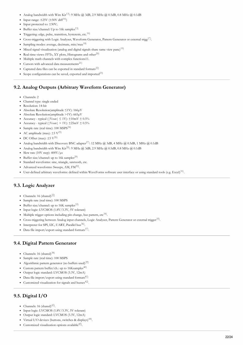
22/24
Analog bandwidth with Wire Kit13): 9 MHz @ 3dB, 2.9 MHz @ 0.5dB, 0.8 MHz @ 0.1dBInput range: ±25V (±50V diff14))Input protected to: ±50V;Buffer size/channel: Up to 16k samples15)
Triggering: edge, pulse, transition, hysteresis, etc.16)
Cross-triggering with Logic Analyzer, Waveform Generator, Pattern Generator or external trigg17).Sampling modes: average, decimate, min/max18)
Mixed signal visualization (analog and digital signals share same view pane)19)
Real-time views: FFTs, XY plots, Histograms and other20)
Multiple math channels with complex functions11.Cursors with advanced data measurements21)
Captured data files can be exported in standard formats22)
Scope configurations can be saved, exported and imported23)
9.2. Analog Outputs (Arbitrary Waveform Generator)
Channels: 2Channel type: single endedResolution: 14-bitAbsolute Resolution(amplitude ≤1V): 166μVAbsolute Resolution(amplitude >1V): 665μVAccuracy - typical (|Vout| ≤ 1V): ±10mV ± 0.5%Accuracy - typical (|Vout| > 1V): ±25mV ± 0.5%Sample rate (real time): 100 MSPS24)
AC amplitude (max): ±5 V25)
DC Offset (max): ±5 V26)
Analog bandwidth with Discovery BNC adapter27): 12 MHz @ 3dB, 4 MHz @ 0.5dB, 1 MHz @ 0.1dBAnalog bandwidth with Wire Kit28): 9 MHz @ 3dB, 2.9 MHz @ 0.5dB, 0.8 MHz @ 0.1dBSlew rate (10V step): 400V/μsBuffer size/channel: up to 16k samples29)
Standard waveforms: sine, triangle, sawtooth, etc.Advanced waveforms: Sweeps, AM, FM30).User-defined arbitrary waveforms: defined within WaveForms software user interface or using standard tools (e.g. Excel)31).
9.3. Logic Analyzer
Channels: 16 (shared)32)
Sample rate (real time): 100 MSPSBuffer size/channel: up to 16K samples33)
Input logic: LVCMOS (1.8V/3.3V, 5V tolerant)Multiple trigger options including pin change, bus pattern, etc34).Cross-triggering between Analog input channels, Logic Analyzer, Pattern Generator or external trigger35).Interpreter for SPI, I2C, UART, Parallel bus36).Data file import/export using standard formats37).
9.4. Digital Pattern Generator
Channels: 16 (shared)38)
Sample rate (real time): 100 MSPSAlgorithmic pattern generator (no buffers used)39)
Custom pattern buffer/ch.: up to 16Ksamples40)
Output logic standard: LVCMOS (3.3V, 12mA)Data file import/export using standard formats41)
Customized visualization for signals and busses42).
9.5. Digital I/O
Channels: 16 (shared)43).Input logic: LVCMOS (1.8V/3.3V, 5V tolerant)Output logic standard: LVCMOS (3.3V, 12mA)Virtual I/O devices (buttons, switches & displays)44).Customized visualization options available45).

23/24
9.6. Power Supplies
Voltage range: 0.5V…5V and -0.5V…-5V46).Pmax (USB powered): 500mW total47)
Imax (USB powered): 700mA48) for each supplyPmax (AUX powered): 2.1W49) for each supplyImax (AUX powered): 700mA50) for each supplyAccuracy (no load): ±10mVOutput impedance: 50mΩ (typical)
9.7. Network Analyzer*³
Shared instruments: Scope, AWGFrequency sweep range: 1Hz to 10MHzFrequency steps: 5 … 100051).Settable input amplitude and offsetAnalog input records response at each frequency52).Available diagrams: Bode, Nichols, or Nyquist53).
9.8. Voltmeters°
Channels (shared with scope): 2Channel type: differentialMeasurements: DC, AC, True RMS54).Resolution: 14-bitAccuracy (scale ≤0.5V/div): ±5mVAccuracy (scale ≥1V/div): ±50mVInput impedance: 1MΩ || 24pFInput range: ±25V (±50V diff)Input protected to: ±50V
9.9. Spectrum Analyzer°°
Channels (shared with scope): 2Power spectrum algorithms: FFT, CZT55).Frequency range modes: center/span, start/stop56).Frequency scales: linear, logarithmic57).Vertical axis options: voltage-peak, voltage-RMS, dBV and dBu58).Windowing: options: rectangular, triangular, hamming, Cosine, and many others59).Cursors and automatic measurements: noise floor, SFDR, SNR, THD and many others60).Data file import/export using standard formats61).
9.10. Other features
USB power option; all needed cables included.External supply option: 5V, 2.5A (not included)High-speed USB2 interface for fast data transferWaveform Generator output played on stereo audio jackTrigger in/trigger out allows multiple instruments to be linked62).Cross triggering between instruments63).Help screens, including contextual help64).Instruments and workspaces can be individually configured; configurations can be exported65).
*³The Network Analyzer instrument in WaveForms uses a channel of Analog Outputs (AWG) and all Analog Inputs (Scope) hardware resources. When it startsrunning, all other instruments using the same HW resources (competing instruments: AWG, Scope, Voltmeters, Spectrum Analyzer) are forced to a BUSY state.When running a competing instrument, the Network Analyzer is forced to a BUSY state
°This instrument in WaveForms uses Analog Inputs (Scope) Hardware resources competing with other WaveForms instruments (Scope, Spectrum Analyzer,Network Analyzer, Voltmeter). When it starts running, the competing instruments are forced to a BUSY state. When running a competing instrument, this instrumentis forced to a BUSY state.
°°This instrument in WaveForms uses Analog Inputs (Scope) Hardware resources competing with other WaveForms instruments (Scope, Spectrum Analyzer,Network Analyzer, Voltmeter). When it starts running, the competing instruments are forced to a BUSY state. When running a competing instrument, this instrumentis forced to a BUSY state.

24/24
1) , 3) , 5) These 16 digital lines are shared by the Logic Analyzer, Pattern Generator and Digital I/O. They are always inputs, some of them can be set to be outputsalso. Digital I/O has precedence in case of output conflict with the Pattern Generator.2) , 4) , 6) , 7) When inputs, these lines can be set to be 1.8V CMOS compatible.8) See note in section 2. Scope9) High Gain: ±2.6V differential input voltage range.10) Low Gain: ±29V differential input voltage range.11) High Gain or Low Gain is used in the analog signal input path for rough scaling. “Digital Zooming” is used for multiple scope scales.12) , 13) The Scope bandwidth depends on probes. The Analog Discovery wire kit is an affordable, easy-to-use solution, but it limits the frequency, noise, and crosstalkperformances (see Figure 21, down). With coax probes and Analog Discovery BNC adapter, the 0.5dB Scope bandwidth is 10 MHz (see Fig. 15).14) As shown in Fig. 12, a ±50V differential input signal does not fit in a single scope screen (ADC range). However, Vertical Position setting allows visualization ofeither +50V or -50V levels.15) Default Scope buffer size is 8kSamples/channel. The WaveForms Device Manager provides alternate FPGA configuration files, with different resource allocation.With no memory allocated to the Digital I/O and reduced memory assigned to the AWG, the scope buffer size can be chosen to be 16kSamples/channel.16) , 17) , 34) , 35) , 62) , 63) Trigger Detectors and Trigger Distribution Networks are implemented in the FPGA. This allows real time triggering and cross-triggering ofdifferent instruments within the Analog Discovery device. Using external Trigger inputs/outputs, cross-triggering between multiple Analog Discovery devices ispossible.18) Real time sampling modes are implemented in the FPGA. The ADC always works at 100Msamples/sec. When a lower sampling rate is required, (108/Nsamples/sec), N ADC samples are used to build a single recorded sample, either by averaging or decimating. In the Min/Max mode, every 2N samples are used tocalculate and store a pair of Min/Max values. The stored sample rate is reduced by half in Min/Max mode.19) In mixed signal mode, the scope and Digital I/O acquisition blocks use the same reference clock, for synchronization.20) , 21) , 36) This functionality is implemented by WaveForms software in the PC, using the buffered data from the FPGA. After a acquiring a complete data buffer atthe FPGA level and uploading it to the PC, the data is processed and displayed, while a new acquisition is started.22) , 23) , 31) , 37) , 41) , 42) , 44) , 45) , 51) , 52) , 53) , 54) , 55) , 56) , 57) , 58) , 59) , 60) , 61) , 64) , 65) This functionality is implemented by WaveForms software, in the PC.24) The AWG DAC always works at 100Msamples/sec. When a lower sampling rate is required, (108/N samples/sec), each sample is sent N times to the DAC.25) , 26) The AWG output voltage is limited to ±5V. This refers to the sum of AC signal and DC offset.27) , 28) The AWG bandwidth depends on probes. The Analog Discovery wire kit is an affordable, easy-to-use solution, but it limits the frequency, noise, and crosstalkperformances. With coax probes and Analog Discovery BNC adapter, the 0.5dB AWG bandwidth is 4MHz (see Figure 21).29) Default AWG buffer size is 4kSamples/channel. The WaveForms Device Manager provides alternate FPGA configuration files, with different resourcesallocation. With no memory allocated to the Digital I/O and reduced memory assigned to the Scope, the AWG buffer size can be 16kSamples/channel.30) , 39) Real time implemented in the FPGA configuration.32) , 38) , 43) All digital I/O pins are always available as inputs, to be acquired and displayed in the Logic Analyzer and Static I/O. The user selects which pins are alsoused as outputs, by the Pattern Generator or Static I/O. When a signal is driven by both Pattern Generator and Static I/O, the Static I/O has priority, except if StaticI/O attempts to drive a HiZ value.33) Default Logic Analyzer buffer size is 4kSamples/channel. The WaveForms Device Manager provides alternate FPGA configuration files, with different resourceallocation. With no memory allocated to the Scope and AWG, the Logic Analyzer buffer size can be chosen to be 16kSamples/channel.40) Default Pattern Generator buffer size is 1kSamples/channel. The WaveForms Device Manager provides alternate FPGA configuration files, with differentresources allocation. With no memory allocated to the Scope and AWG, the Pattern Generator buffer size can be 16kSamples/channel.46) WaveForms allows setting the user voltages in the range 0V…5V respectively -0V…-5V. However, voltages below 0.5V, respectively above -0.5V might haveexcessive ripple and should be used with caution.47) This limit results from the overall device power balance: the power available from the USB port, minus the power internally used by the device, moderated by theuser power supplies efficiency. The balance of 500mW is available for both user supplies to share.48) , 49) , 50) This limit results from the structure of each user power supply (positive and negative). It is not conditioned by the load degree of the complementary usersupply.
analog_discovery_2/refmanual.txt · Last modified: 2015/10/02 10:07 by Mircea Dabacan