1 introduction - slac
TRANSCRIPT

Sensor Concepts for Pixel Detectors in High EnergyPhysics
Tilman RohePaul Scherrer Institut5232Villig enPSISwitzerland
Abstract
Differentapproachesin thedesignof pixel sensorsfor variousexperimentsin par-ticle physicsarereviewed. A shortoutlook of potentialdevelopmentdirectionsforfutureexperimentsis alsogiven.
1 Introduction
Hybrid pixel detectorsconsistof a thin, segmentedsilicon sensorwith highly segmentedintegratedreadoutchipsconnectedto it via thebumpbondtechnique.Thesensoris seg-mentedinto pixels of about
areaandthe readoutchip is subdivided into pixel
unit cellsmatchingthesensorpixels.While theR&D effort is focusedmainlyon thechal-lengingreadoutelectronicsandbump-bondingtechnique,lessattentionwasinitially givento thesensor. For thefirst generationpixel detectors,theproventechniqueof silicon stripdetectorswasmerelyadapted.Theneedof a very high level of radiationtolerancein theLHC experimentshowever triggeredan extensive R&D programboth for strip andpixelsensors,with the pixel sensorsrequiring the highestdegreeof radiationhardness.Thispaperreviews pixel sensorconceptsfor variousenvironmentsin high energy physicsex-perimentsin thepastandpresent,anddiscussesthelimitationsof thedifferentapproaches.Therequirementsof possiblefutureexperimentsareshortlymentionedandsomefieldsofpresentresearcharesummarized.
2 First Generation Pixel Detectors
Thefirst generationpixel detectorse.g. theonesof WA97 [1] andDELPHI [2] usedDC-coupled“p in n” sensorsassketchedin fig. 1. The pixelsarep -implantsin an n-typesubstrateforming a pn-junction. As the p -side’s metallizationis directly connectedtopixel-implants,no costdriving featureslike poly-resistorsor largeareacapacitorshave tobe implemented.The backsideis connectedvia an ohmic contactrealizedby an overall
1

Neff
V
ohmic n−side
p−side sensor
E
readout chip bumpunder bump metalaluminiumoxideboron implant
Figure1: Crosssectionof a p in n pixel detector. The effective dopingandthe electricfield at full depletionvoltageis alsoindicated.Thedimensionsdo notscalecorrectly.
n -implantandanaluminization.Thesesensorsrequireonly four masklayersand– mostimportant– no photolithographicstepon the backside.Thereforethey arecalledsinglesided.
Whenapplyinga positive backsidevoltagethe sensitive spacecharge region startstogrow from thepn-junctiononthestructuredsideof thesensoruntil it is stoppedby thehighdosen -implantat thebackside.Thefield createdby thejunctionin thefully depletedstateis sketchedontheright sideof fig. 1. It’ smaximumis closeto thecollectingelectrodewhileit vanishesat thebacksidecontact.Thereforethedevicecanbeoperatedpartiallydepleted.Thismightbecomenecessaryif thebacksideis mechanicallydamagedandanextensionofthedepletionzoneinto thedamagedregionwould leadto anunacceptablecurrentincrease.
Sinceradiationhardnessis not an issuein the applicationsdiscussedin this section,usuallya low dopedfloat zonen-substratewith a resistanceof several Ω is used.Thisleadsto a full depletionvoltagebelow . The high voltagestability of the devicesis not critical andguardring structureswith oneor two rings aresufficient. Due to thelow operationvoltage,thesmall distanceof onebumpdiameterbetweenthe sensoredgebeingon backsidepotentialandthegroundededgeof thereadoutchip is uncriticalandnosparkingbetweenbothpartshasbeenobservedin this kind of devices.
2.1 Pixel Layout
A possiblelayoutof apixel cell is sketchedin fig. 2. It consistsonarectangularp -implant,with themetalizationcoveringalmostthewholeimplantedarea,andabroadcontactopen-ing. Thepadsfor bumpbondingarelocatedat theendof thepixel andareoftenarrangedin amirroredgeometryasindicated.
Whereasthepitch is givenby therequiredspatialresolutionandthebumppadpositionby thedesignof the readoutchip, the implantwidth is a “layout decision”. It determines
2

!!!!!!
""""######$$$$
ContactBump
ImplantMetal
Pitc
h
Wid
thG
ap
Figure2: Possiblelayoutof apixel cell.
A
+ −
p−side
n−side
n−bulk
PixelsGuard rings
Probe
depletion zone
Figure3: IV-setupfor a simplep in n sen-sor.
bias [V]%0
&20'
40(
60)
80*
100+
Rev
erse
Cu
rren
t [A
]
0&0.05
& 0.1&0.15& 0.2&0.25& 0.3&0.35& 0.4&0.45& 0.5& -7x10
Delphi pixel sensor w930l
Figure4: MeasuredIV-characteristic[4].
thecapacitancebetweenneighboringpixels. Thenoisein thepixel preamplifieris mainlydeterminedby it’ s capacitive load. The total capacitanceof a pixel is dominatedby thecapacitancetowardsit’ s neighbors. This canbe decreasedby increasingthe gapwidth.In orderto keepthe pitch unchanged,the implant width hasto be decreasedat the sametime. In “strip like” pixel geometrieswith a largeaspectratio asshown in fig. 2, only twoof theneighborscontributesignificantlyto overall capacitanceandthereforeonly thegapindicatedin fig. 2 needsto bemaximized.However if onetries to pushthis approachtoofar thechargecollectionwill beaffectedandthesignalcouldbeoutof time [3].
2.2 Sensor Testing
Usuallypixel detectormodulesconsistof severalreadoutchipsplacedononesensor. Afterthis procedureall the pixel cells on the sensoraregroundedvia the bump bondsandthechips.As thechipsarethemostexpensivepartof apixel detector, it is of interestto testthesensorbeforeattachingit to severalreadoutchips.Theeasiestmethodfor testingsensorsisto takeanIV-curve,sincealreadysmalldamagesleadto anincreaseof theleakagecurrent,if they areinsidethe spacecharge region. In orderto fully depletethe sensor, all pixelsmust be contacted. As it is impossibleto contacteven a small fraction of the roughly50000 pixel cells in a highly segmentedsensorwith a probecard,e.g. in the DELPHI
3

experimentonly the guardcurrentwasmeasuredassketchedin fig. 3. A measurementperformedduringtheDELPHI moduleproductionis shown in fig. 4 [4]. In thefirst partthecurrentdisplaystheusualsquareroot likebehavior asthedepletionzonegrows just belowthedirectly biasedguardrings. During themeasurementthedepletionzoneexpandsalsolaterallyandpunchesthroughto thefirst row of pixelsatabout , - . Fromthisvoltagethedepletionzonealsogrowsbelow thesepixelsasindicatedin fig. 3 andthedepletedvolumeis much larger leadingto a highercurrentlevel asvisible in fig. 4. The punchthroughbetween . and / to the next pixel row is lessclearly visible. The breakdown atroughly , / is probablynotdueto any sensordamagebut dueto highfieldsin thepunchthroughregions.As at , 0. only asmallpartof thesensoris depleteddueto lateralpunchthrough,mostpixelsanda large fraction of the backsideremainuntested.However, thismethodis capableto detect“obviouslyfaulty” devicesthatshow amuchhighercurrentanddifferentshapeof thecharacteristic.At theendof themoduleproductionof theDELPHIpixel detectorabout8% hadto berejectedbecauseof high leakagecurrentand5% duetohighnoise[5]. Which fractionof thosecouldhavebeenavoidedby moreadvancedsensortestingis unknown.
3 Radiation Induced Effects in Silicon
In theexperimentsdiscussedup to now radiationhardnesswasnot required.This changeswhenmoving to high rateexperimentswith hadrons. In the context of LHC (andSSC)radiationinducedeffectshave beensystematicallystudiedsincethe late1980s[6, 7, 8, 9,10]. Usuallyadistinctionbetweencrystaldamagein thesensorvolume(bulk damage) andeffectsat theinterfaces(surfacedamage) is made.
3.1 Bulk Damage
As silicon andothersemiconductorsarecrystalsit is expectedthat they will suffer fromradiationdefects. High energetic particleswill not exclusively interactwith the electroncloudproducingtheelectricalsignalbut alsowith thenucleioftendisplacingthemout ofthelattice. This producescrystalimperfectionsthatmaybeelectricallyactive andchangethe electricpropertiesof the material. In the inner regionsof high ratehadronicexperi-mentsthe concentrationof crystaldefectswill after someyearsof operationexceedtheinitial substratedoping.At this momentthematerialpropertieswill bemainly determinedby thedefects.Eventhoughit is not yet possibleto correlateall changesin theoperationparametersof thesensorswith specificmicroscopicdefects,thesechangeshavebeenstud-ied in detail. This allows a predictionof all the importantsensorparametersfor a givenradiationscenario[8, 11,12, 13]. Themostimportantquantitiesinfluencedby bulk defectsareshortlysummarizedin thefollowing.
4

13254 6 798;: <9=?> @9A;B CEDGFF HJILKNMPORQTSVU5WYX ZV[
\]\9^] ^\9^5^] ^5^\9^;^;^] ^;^;^
_;` abc defgihjkk m
lm
nToqp rsTtquvTw;xyTzq|Tq~
» T5» T5 J J¡ ¢ £¤¥ ¦
§0¨;© ª«§5¬§0¨;© ª«§5¬®¨;© ªq§;¬®¨;© ªq§;¬
© ª§G¬°¯ q±G¬T²´³¯ µ«© ª§G¬°¯ q±G¬T²´³¯ µ«
Figure5: Changeof the full depletionvolt-ageof a ¶ 0 µ
thick siliconsensor[8].
1 10 100 1000 10000
annealing time at 60oC [min]
0
2
4
6
8
10
∆ N
eff [
1011
cm-3
]
NY,∞ = gY Φeq
NC
NC0
gC Φeq
NA = ga Φeq
Figure6: Annealingbehavior of the effec-tivespacechargeafterirradiationwith aflu-enceof , i·¸ , V¹»º ½¼
[12].
Leakage current: The leakagecurrent increasesproportionally to the fluenceof thechargedparticles.As theleakagecurrentis stronglytemperaturedependent,irradiatedsen-sorshave to becooledduringoperationin orderto prevent thermalrunaway which mightbedestructive.
Full depletion voltage: The full depletionvoltagechangesduring irradiationasshownin fig. 5. In the first part up to several , V¹ ½¼
it is decreasingasthe processof donorremoval is dominant. At a higherfluencethe creationof radiationinduceddefectswithnegative spacecharge becomesdominant,leadingto a spacecharge sign inversion(alsocalledtypeinversion).Thedepletionzoneafterthisfluencestartsto grow from then -sideof thesensor. Thetotal spacechargemainly causedby theradiationinduceddefectsis re-ferredto astheeffectivedopingconcentration.As it increasesproportionallyto thefluence,thefull depletionvoltagealsoincreases.In orderto keepthesensitivevolumeconstant,theappliedvoltagehasto besteadilyincreasedup to valuesof severalhundredvolts. As theenergy levelsassociatedto thosedefectsarelocateddeepin thebandgap,they donotcon-tribute to the conductivity, and irradiatedsilicon featuresonly the intrinsic conductivity.Theeffectivedopingconcentrationdisplaysacomplex annealingbehavior shown in fig. 6,commonlydescribedby theHamburg model[12, 14]. After irradiationtheeffectivedopingconcentrationdecreasesto a minimum(stabledamage,¾0¿ÁÀ in fig. 6) reachedafteraboutoneweekat roomtemperature(beneficialannealing)andslowly increasesafterwards(re-verseannealing).In orderto slow down this increase,irradiateddetectorshave to bekeptcoolalsooutsiderunningperiods.
Extensivework hasbeendoneto evaluatewhetherthepost-irradiationpropertiescanbeaffectedby specificimpuritiesotherthanboron,phosphoror arsenic.It wasfoundthatanenrichmentof thesilicon substratewith oxygen,which is believedto capturevacanciesinstableandelectricallyneutralpointdefects,leadsto asuperiorpost-irradiationperformance
5

for samplesirradiatedwith chargedhadrons[13, 15]: The increaseof the full depletionvoltageafter irradiationinducedspacecharge sign inversionis reducedby abouta factorof 4 comparedto non-oxygenatedfloat zonematerial. Furthermorereverseannealingissloweddown by a factorof two andits amplitudeis reduced.As themain fluencein theinnermostpartof theexperimentsathadroncolliders,wherepixel detectorsarecommonlylocated,is dueto chargedpions,theuseof oxygenatedmaterialis recommendedthere.
Trapping Radiationinduceddefectsactalsoaschargetrappingcenters.Trapsaremostlyunoccupiedin thedepletionregion dueto the lack of freechargecarriersandcanhold ortrap partsof the signal charge for a time longer than the charge collection time andsoreducethe signalheight. The inversetrappingtime is proportionalto the concentrationof trapsand thereforeproportionalto the fluence. Trappingtimes in irradiatedsiliconhave beenmeasuredfor electronsandholes[16]. Holesaremoreproneto trappingthanelectronsandthereforethecollectionof electronsis preferredfor applicationsin veryharshradiationenvironment. A complex modelhasbeenbuilt to predictthedependenceof thecharge collectionefficiency on the trappingtime and the electric field inside the sensor[11]. For most of the tracking devices usedin particle physicsthis effect is much lessof a problemthantheradiationinducedeffectsmentionedabove. However if theparticlefluenceapproachesor evenexceeds, ¹»Â ¼
thechargecollectionefficiency degradedbytrappingwill bethelimiting factorof silicon devices[17].
3.2 Surface Damage
In siliconthesurfaceregionis alsosensitiveto radiation.Thetermsurfacedamagesumma-rizesall defectsin thecoveringdielectrics,e.g.thesiliconoxideandtheinterfacebetweenthesilicon andthe dielectric. As thecrystalstructureof silicon oxide is highly irregular,displacementof singleatomsdueto irradiationdoesnot leadto macroscopicchanges.Ion-ization in the oxide however is not fully reversibleandmay causesteadychangesof theinterfaceproperties.Oneconsequenceof ionizationin theoxide is thebuild up of a pos-itive fixedoxidecharge that saturatesafter somekGy at a valueof about ¶ ¸ , ¹ ÄÃÅ Æ[18, 19, 20]. This oxide charge changesthe electricfield in the silicon bulk closeto thesurfaceand inducesa compensatingelectronaccumulationlayer in n-type silicon andadepletionlayerin p-typematerial.
A further effect of radiationis the generationof interfacestatesleadingto a surfacegeneratedcurrentwhenthespacecharge region reachesthesurface. This contribution tothedarkcurrentis proportionalto theareanotcoveredby thepixel implants[20].
6

metal overlaps tosurpress current reduce fields
edge (positively biased)
hole current
sensitive area
Figure7: Schematiccrosssectionof a pos-sibleguardring designwith metaloverlapsaccordingto [22, 23].
µ20 m
depletionzone
readoutchip
sensor
0 V
n−side
p−sideV
VV
pixelsguard rings
chip’s wire bond padsand metal lines (0V−5V)Ç
Figure 8: Depletion region below guardringsandpotentialof surfacesandedges.
4 Radiation Hardness of p È in n Sensors
In anunirradiatedp in n device thedepletionzoneis growing from the junctionson thestructuredp -side.After thespacechargesigninversionthedepletionzonestartsto growfrom the the unstructuredbackside.As long asthe depletionregion hasnot reachedthesurface,all pixelson thep -sideareconnectedvia the invertedundepletedbulk material.As this materialhasa poorconductivity, it is transparentto fastsignals.This meansthat“p in n” sensorsirradiatedover the point of inversiondeliver spatialinformationevenwhenoperatedslightly under-depleted[21]. However thesignalsbecomevery smallwithincreasingunder-depletionand thereforeit is not advisibleto rely on this featurein anexperiment. The useof p in n sensorscan only be recommendedif the radiationandtemperaturescenariopredictsa full depletionvoltagewhich canrealisticallybe applied.Thereforeradiationhardnessbecomesequivalentto high voltagecapability. In thecomingsectionssomemeasuresto increasethehighvoltagestabilityarediscussed.
4.1 Guard Rings
Thepurposeof a multi guardring structureis to establisha gradualvoltagedropbetweenthesensitiveregionongroundpotentialandthecuttingedgeonbacksidepotential.It avoidshigh fields andsubsequentbreakdown at the device edgeandpreventsthe spacechargeregion from reachingtheheavily damagededgeregion. Floatingringsbiasthemselvesviathepunchthroughmechanism.Thepotentialdropbetweentheringscanbeinfluencedbytheir spacinganda metaloverlap. Field platesdirectedoutwardsreducetheelectricfieldat the implant edge. This is a techniqueusedin power electronicssincethe late 1960’s[24]. However it alsoreducesthepunchthroughvoltagebetweentwo neighboringringsifit coverstoo muchof thegap.Thereforetheseoverlapsareusuallykeptrelatively smallasindicatedin fig. 7. A field platedirectedtowardsthesensitive regionsuppressesthepunch
7

throughholecurrentandincreasesthepunchthroughvoltage[22]. Thiscanbeunderstoodin termsof ap-MOSFETwith thegate(largefield platedirectedinwards)connectedto thesource(theouterof eachtwo rings). Suchgeometriesarethereforepreferredover designsusingoutwardsdirectedfield plates[23].
Thenumberof guardringsnecessarydependson themaximalbiasvoltagetargeted.Ifa uniform potentialdropbetweentherings is aimedfor, thespacinghasto increasefromtheinnerto theouterregions.Althoughthereis alwayssomepressureto haveasmalledgeregionin orderto minimizedeadmaterial,ausefulrule-of-thumbis to foreseeadistanceofroughlythreetimesthewaferthicknessbetweenthecuttingedgeandthesensitiveregion.
It hasto bementionedthata reliableedgeterminationcanalsobeobtainedwith onlytwo guardrings,oneverycloseto theedgeonbacksidepotentialandoneverycloseto thesensitive region on ground.Both ringshave to beconnectedvia a highly resistive (but notperfectlyisolating)passivationcovering thewholeoxidesurfacein betweento guaranteea well definedand gentlepotentialdrop. However sucha passivation is not offeredbymostsensorvendorsandtheuseof sucha concepthasto becarefullydiscussedwith theprocessingfoundry.
4.2 Module Concept
Thehigh voltagecapabilityis not only determinedby thesensoritself but alsoby systemaspects.In mostmoduleconceptsfollowedfor hybrid pixel detectors,thewire bondpadsof readoutchipsoverlapthesensoredgesasindicatedin fig. 8, andthechipapproachesthesensorto a distanceof about
0.µ. Thesizeof this gaplimits thehigh voltagecapability
of thedeviceasthebreakdown voltageof air (of theorderof , -ÉÅ µ [25]) caneasilybereached.This is oneof thereasonswhy in applicationsrequiringhigh voltageoperationadoublesidedconceptwith guardringson thebacksideis chosen.
4.3 Limits in Radiation Hardness
Dueto their simplicity, p in n sensorsarethefirst choicefor mostdetectorapplications,especiallythosewhereradiationdamageis notanissueasfor exampleWA97 [1], DELPHI[2] or Alice [26].
In thesesystemshigh resistive silicon is usedandthe operatingvoltageis alwaysfarbelow 100V. However, if onewantsto exploit thelimits in radiationhardnessof thissensortypeasdoneby silicon strip detectorse.g. in theCDF layer00 [27], ATLAS [28] or CMS[29], oneneedsoperationvoltagesof ¶ /ÉÊ / andis facedwith the limitationsgivenby the moduledesignas mentionedabove. This problemmight be solved by avoidingoverlappingchips or addingon top of the sensorsa dielectric layer that standsseveralhundredvolts. The MCM-D technique[30] seemsa goodcandidatefor sucha solution(section6). If it is foundto bepractical,operationof p in n sensorscaneasilybeextended
8

0V µ
20
m
0V
external ground pad
readout chip
controlledbias voltage (>200V)
guard rings
potential drop
n−side isolationpixel implantsn−implanted
edge region
bump bond
sensorback side p−implant
Figure9: Guardring conceptof n in n sensors.Thebiasvoltageis appliedonthesensor’sjunctionside.Thissideof thesensorcontainsalsothemulti-guardring structureprovidinga controlledpotentialdrop towardsthe edge. The whole sensorside facing the readoutelectronicscanbeheldat groundpotential.
into therangeofËÊ ¶ ¸ , ¹ÌÄÍÏÎÐ Å
. Thelimitation for suchdevicesis givenfirstly bytheriseof thefull depletionvoltageandsecondlyby signallossdueto trapping.
5 High Luminosity Experiments with Hadrons
Therequirementsof theLHC experimentsATLAS [31] andCMS [32], andof BTeV [33]atFermiLabin termsof radiationhardnesscannotbefulfilled with thepreviouslydiscussedp in n sensors.At theendof thetargetedlifetime of thedetector, a full depletionvoltageof morethan , // is expected.As themaximumbiasvoltageforeseenis in theorderofÑ/0ÒÊÔÓ0/
, anunder-depletedoperationof thesensorsis requiredfor asignificantpartoftheir lifetime. To copewith thisproblem,all experimentsmentionedhavechosenthen onn conceptfor their pixel sensors.Thepixelsconsistof n -implantationsin high resistivityn-typesilicon while the pn-junction is locatedon the sensor’s backside,surroundedby amulti guardring structureasindicatedin fig. 9. After radiationinducedspacechargesigninversion,thedepletedregionstartsto grow fromthen -sideandthedevicecanbeoperatedpartially depleted,if full depletioncannotbereachedany more. Furthermore,thedouble-sidedprocessingof n in n detectorsallows a guardring conceptwhich keepsall sensoredgesat groundpotentialandavoids the risk of disruptive dischargesto the very closelyspacedfront-endchip. This canbeachievedby placingthemulti-guardring structureonthep-side,i.e. thesensor’s backside.Theouterregion of then -sidecontainingthepixelcells is coveredwith a largen -implant,groundedexternallyvia thereadoutchip. For thedesignof theguardringstheconsiderationsfrom section4.1arestill valid.
In comparisonwith standardp in n sensors,n in n sensorsareroughly twice asex-pensivedueto theneedfor doublesidedprocessingandinter-pixel isolation.Furthermore,
9

− − − −− − − − − −+ + + + + + + + + +
aluminium
n implanthigh field region
p−stop
oxide
(a)p-Stops
−−− −−+ + +++
aluminium
n implant
oxide
high field region
p−spray
(b) p-Spray
+ + + ++− − − −−
p−spray
oxidenitride
aluminium
p−spray with reduced dosen implant
(c) moderatedp-Spray
Figure10: Isolationtechniquesfor adjacentn -implants. Fixed( Õ ) andfree( Ö ) chargecarriersareindicated.Thefield maximaarelocatedat thelateralpn-junctions
a lower yield comparedto singlesideddeviceshasto beexpectedandaneffective sensortestingbeforebump bondingis very important. As a direct probingof all pixel cells isnot possible,somebiasingstructurehasto be integratedonto the sensoritself. Possibleimplementationsarediscussedin thecontext of thepixel designsin section5.2.
5.1 Inter Pixel Isolation
In contrastto the p-side, were the isolation of the adjacentp -implantsis provided bythe omnipresentelectronaccumulationlayer, exactly this accumulationlayer electricallyconnectsthe n -implantsof the n-side if no precautionsare taken. Isolation is usuallyprovidedby a boronimplantbetweenthepixelsforming a lateralpn-junction. Dependingon thedosethis isolationimplantis calledeitherp-stopor p-spray.
5.1.1 p-Stop Isolation
In doublesidedstripdetectors,acommontechniqueis to introduceahighdosep -implantbetweenthe stripsasshown in fig. 10a. This is doneby an additionalphotolithographicstep.Thealignmentof thep-stopmaskwith respectto then -pixelsis critical asanover-lappingof the two high doseimplantswould result in Zenerbreakdown. The minimumspacingbetweentwo n -implantsis thereforelimited by the necessaryalignmenttoler-ances.Theadvantageof this techniqueis thata typical doseof about , ¹Ì boronionspersquarecentimeterwill in any caseguaranteegoodisolationalsoaftertheradiationinducedbuild-up of a positivesurfacecharge,andtheadjustmentof theimplantationdoseis not atall critical.
Theelectricfield closeto thelateralpn-junctionwasnumericallycalculatedusingatwodimensionaldevice simulationpackage[34]. Theun-irradiateddevice hasa very low ox-ide charge,resultingin a low electricfield. Thevalueof theoxidechargeincreasesafterasmallirradiationdoseof below
0 ×ËØ to its saturationvalue,resultingin anaccumulation
10

of electronscloseto thesurfaceandconsequentlyin a strongincreaseof theelectricfield.The potentialof the p-stopdependson the implant geometry, the backsidebiasand thesubstratedoping. As thetwo lattervaluesalsoarevery high in a highly irradiatedsensor,thepotentialdifferencebetweenn -pixelsandthep -stopsincreaseswith ongoingirradi-ation,leadingto anadditional,but lessdrastic,increaseof theelectricfield. Theoperationof devicesfeaturingp-stopsin a strongradiationfield is limited by their decreasinghighvoltagecapability.
5.1.2 p-Spray Isolation
If thedoseof theboronimplantis matchedto thesaturationvalueof theoxidechargewhichis of theorderof ¶ ¸ , V¹ ÃÅ ½¼
, theboronconcentrationis sosmall, thatanoverlapoftheboronimplantwith thepixel’s n -implantdoesnot leadto breakdown. Thereforethemaskseparatingboth implantationscanbeomittedandthewholesurfaceis thencoveredby themediumdoseboronimplant. At theplacesof thepixels thehigh dosen -implantis not compensated.Becauseof themissingmaskthis techniqueis calledp-sprayisolation[34]. Theabsenceof a photolithographicstepis a costadvantageandalsopermitsnarrowspacingbetweenneighboringn -implants,asthereareno alignmenttolerancesbetweentwo differentmasksto bekept.
The point of maximal electricalfield is the lateralpn-junction betweenthe isolatingboronimplantandthe n -pixelsasindicatedin fig. 10b. Theun-irradiateddevice showsthehighestelectricalfield andthereforethelowestbreakdown voltagein its life cycle. Withtheincreaseof theoxidechargeto its saturationvaluetheshallow p-spraylayermovesintothedepletedstateandtheelectricfield decreases.Thelowestelectricfield is reachedwhentheboronimplantmatchesexactly thesaturationvalueof theoxidecharge.However if theimplantationdoseis too low the isolationmight not be sufficient. Thereforeoneusuallychoosesanimplantdoseabit higherthannecessaryto preventfailurein caseof fluctuationsin theproductionprocess.With thefollowing increaseof theeffectivesubstratedopingtheelectricfield shows anuncritical increase.Thereforethesedevicesarecharacterizedby animprovedhighvoltageperformanceafterirradiation.
In order to improve the pre-radiationhigh voltagestability of p-spraydeviceswhilekeepingtheir good post-irradiationbehavior, the moderated p-spraytechnique[35] hasbeendeveloped. Here the p-sprayimplant is performedlater in the productionprocess.A topographyon the wafer’s surface,asfor exampleobtainedwith a nitride layer shownin fig. 10c,will thenbe reproducedin thedopingprofile asindicated.Theborondoseinthemiddleof thegapbetweentwo pixelscanbechosenhigh enoughto ensureinter pixelisolation,e.g. twice theexpectedsaturationvalueof thesurfacecharge. At thesametimetheborondosein thesurroundingof the lateralpn-junctioncanbeoptimizedfor thebesthigh voltageperformancewhich is reachedwhenthe doseis closeto the expectedsatu-ration valueof the surfacecharge. As the nitride layer is a standardstepin the processof many detectorvendorsthis technologyin mostcasesdoesnot needan additionalpho-
11

tolithographicstep. However, the freedomto designvery small gapsbetweenthe pixelimplantsis limited in themoderatedp-spraytechnologyasthemoderationis only effectiveif thelayerof themoderatedp-spraydosehasaminimumwidth of about ¶ Ê µ
.
5.2 Pixel Layouts
Thelayoutof thepixel cell dependsstronglyon then-sideisolationtechnique.Thereforebothmethodsarediscussedseparately.
5.2.1 Layouts with p-Stops
Whendesigninga p-stopisolateddevice, mostattentionis paid to thegeometryof thep-stops.For strip detectorsnumerousgeometrieshave beenevaluated[36, 37]. However inpixel devices“atoll” like structuresarepreferredin orderto avoid local defectsaffectingthewholearray[38]. Ù -stopsprovide a very goodisolation.However, in somesituationsahigh resistiveconnectionbetweenthepixelsis desirable,for exampleto performIV-testsof thedeviceson wafer level, or to hold unconnectedpixelscloseto groundwhenthefulldepletionvoltageis exceeded.In caseof anohmicconnectionbetweenneighboringpixels,themaximumvalueis determinedby themaximumacceptablevoltagedropbetweenpixelsandtheleakagecurrent,leadingto avalueof theorderof ,Ú× Ω. Thelowerlimit of theinter-pixel resistanceis givenby the requirementof preventinga significantsignaldistributionto the neighborchannelswithin a typical shapingtime of 25ns. This leadsto a lowerlimit of the resistanceof about ,ÚÛ Ω. Resistorscanbe implementedby openingsin thep-stopimplantssurroundingevery pixel cell, which leave room for a conductive electronaccumulationlayer. Thevalueof theresistancedependsonthelengthandthewidth of thispath. Dif ferentpossibleresistorgeometriesshown in fig. 11 have beenevaluated[39, 40,41].
Thevalueof theresistancedependsvery stronglyon thebacksidevoltageasshown infig. 12. At low voltagesthecurrentflows mainly throughtheundepletedbulk. Whenthespacecharge region reachesthe n-side, the pixels areseparatedfrom eachotherandthecurrenthasto passthroughtheelectronaccumulationlayerformingtheresistor. This leadsto an increaseof the resistanceasseenin fig. 12 around ,R (onep-stopring). Whenthe bias voltageis increasedfurther the resistancefirst grows slowly for a while beforeincreasingvery steeplyabove
0/. This is indication of pinch-off, sincewith further
over-depletionthepotentialdifferencebetweenp-stopsandthen -implantsincreasesandafield is growing from thepn-junctionbetweenp-stopsandbulk alsoin thelateraldirection.Thewidth andheightof the“plateau”region between150and
®/dependsstronglyon
thep-stopgeometry. In the“one-ring-design”(fig. 11(b))it is well developedwith awidthof almost at roughly ,ÚÛ Ω. Consequentlyit is possibleto over-depleteall pixelsby usingtwo probeneedles,oneplacedon thep- sidediodeandtheotheron then-sideguardring. This allows for a reliablesensortesting. In the “two ring design”shown in
12
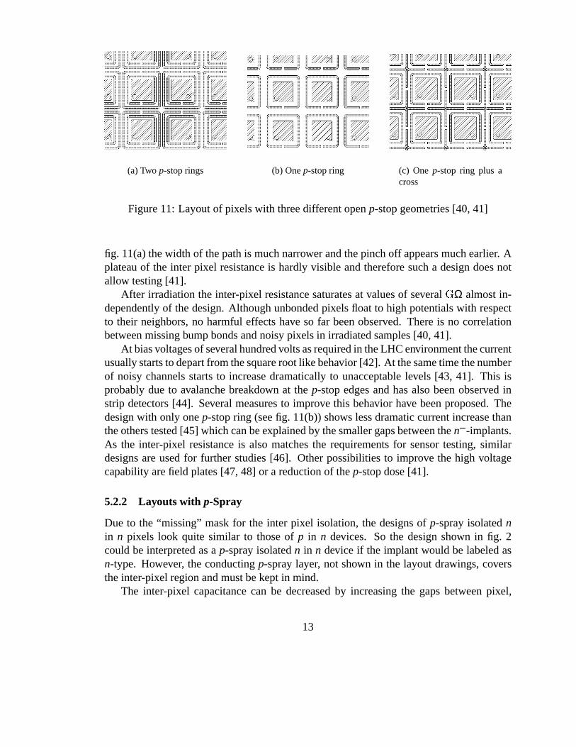
(a)Two p-stoprings (b) Onep-stopring (c) One p-stop ring plus across
Figure11: Layoutof pixelswith threedifferentopenp-stopgeometries[40, 41]
fig. 11(a)thewidth of thepathis muchnarrowerandthepinchoff appearsmuchearlier. Aplateauof the inter pixel resistanceis hardlyvisible andthereforesucha designdoesnotallow testing[41].
After irradiationthe inter-pixel resistancesaturatesat valuesof several × Ω almostin-dependentlyof thedesign.Althoughunbondedpixelsfloat to high potentialswith respectto their neighbors,no harmful effectshave so far beenobserved. Thereis no correlationbetweenmissingbumpbondsandnoisypixelsin irradiatedsamples[40, 41].
At biasvoltagesof severalhundredvoltsasrequiredin theLHC environmentthecurrentusuallystartsto departfrom thesquarerootlikebehavior [42]. At thesametimethenumberof noisy channelsstartsto increasedramaticallyto unacceptablelevels [43, 41]. This isprobablydueto avalanchebreakdown at the p-stopedgesandhasalsobeenobserved instrip detectors[44]. Severalmeasuresto improve this behavior have beenproposed.Thedesignwith only onep-stopring (seefig. 11(b))shows lessdramaticcurrentincreasethantheotherstested[45] whichcanbeexplainedby thesmallergapsbetweenthen -implants.As the inter-pixel resistanceis alsomatchesthe requirementsfor sensortesting,similardesignsareusedfor further studies[46]. Otherpossibilitiesto improve the high voltagecapabilityarefield plates[47, 48] or a reductionof thep-stopdose[41].
5.2.2 Layouts with p-Spray
Due to the “missing” maskfor the inter pixel isolation,the designsof p-sprayisolatednin n pixels look quite similar to thoseof p in n devices. So the designshown in fig. 2couldbeinterpretedasa p-sprayisolatedn in n device if the implantwould be labeledasn-type. However, theconductingp-spraylayer, not shown in the layoutdrawings,coverstheinter-pixel regionandmustbekeptin mind.
The inter-pixel capacitancecan be decreasedby increasingthe gapsbetweenpixel,
13

0 50 100 150 200 250104
105
106
107
108
Vbias [V]
R [
Ω]
one p-stop ringtwo p-stop rings
Figure 12: Bias dependenceof the inter pixel resistancefor the two designsshown infig. 11(b)and11(a)[40, 41].
however otherconsiderationsfavor small gaps. Sincethe mostimportantrequirementton in n sensorsis radiationhardness,the deviceshave to be optimizedfor high voltageoperation.In orderto achieve this, theelectricfieldshave to bekeptassmallaspossible.Thereforethe potentialdifferencebetweenthe p-spraylayer and the pixel’s n -implantmustbelimited, asthelateralpn-junctionis themostcritical spotin thesedevicesin termsof electricalbreakdown. Thepotentialof thep-sprayis determinedby thelargestdistancebetweenneighboringn -implantsanywhereon thedevice. Theseareusuallythediagonalgapsin theregionswherefour pixels join. In conclusiontheuseof thesmallestgapsstillcompatiblewith noiserequirementsis recommended(typically 15 -
0µ
).Thetechnologicalpossibilityto realizeevensmallergapsbetweenthen -implants(typ-
ically µ
) canbeusedto implementa punchthroughbiasgrid asshown in fig. 13. In anun-irradiatedsensorall pixelsareconnectedwith eachotherandto thebiasgrid throughthebulk, aslong asthebiasvoltageappliedis below full depletion.Whenthefull deple-tion voltageis exceeded,all n -implantsareisolatedby thep-spraylayerandthe leakagecurrentof eachpixel hasto flow to the biasgrid throughthe depletedbulk via thermo-ionic emission.Dueto thenarrow spacingthepotentialdifferencebetweena pixel andthebiasgrid cannotexceedmorethana few volts andthegrid canbeusedto biasall pixels.An IV-curve takenwith two probeneedlesis capableto detectmostfrequentfailures,e.g.scratchesor spikesanywherein the sensitive volume. After bump-bondingthe biasgridis out of function becausethe pixels arebiasedvia the readoutchip. For this reasonnoadditionalnoisehasbeenobservedin pixel detectorsusingthis featurein contrastto irradi-
14

Figure13: Two possibleimplementationsof apunchthroughbiasgrid [43].
atedsiliconstripdetectorswith punch-throughbiasing[49, 21]. In caseof amissingbumpbondtheunconnectedpixel is keptcloseto groundpotentialby thebiasgrid andwill notaffect theneighbors.Thebus line of thebiasgrid will collect somesignalcharge,whichwill be lost, andtheparticledetectionefficiency will bereduced.It is thereforedesirableto minimizetheareacoveredby thebiasstructure.
Theimplementationshown in fig. 13ais themostsimpledesignwith leastrequirementsto theproductionprocess.Thereareno smallstructuresthatcouldapproachthe limits ofthetechnologyandall metalareasareunderlayedwith animplant.Soevenpinholesin theoxidewould not causeharm. In thedesignshown in fig. 13btheareaaffectingthechargecollectionis minimized. The implantationof thebiasstructureis shrinkedto a smallbiasdot placedinside the pixel. Surroundingthe bias dot with the pixel implant guaranteesthat the signalgeneratedin the region betweenthe pixels is not lost to thegrid. The busin-betweenthe pixels is just a metal line. Testbeammeasurementswhich suchdevicesshow a particledetectionefficiency above 99% in the un-irradiatedstate[50] andabove95% after irradiationwith , ¹»Â ÍÏÎÐ Å Ü
[51]. However, sucha designis moredemandingconcerningthefabricationprocess.
For devicesfeaturingmoderatedp-spraythedesignconsiderationsaresimilar. Duetothe alignmenttolerancesandin orderto effectively reducethe electricfield with a lowerboronconcentration,a certainminimal distancebetweenthe pixel’s phosphorusimplantandthenitride edgehasto beprovided. If onetriesto implementa biasgrid accordingtofig. 13aonewouldobtainatoo largepunchthroughvoltagebetweenthegrid andthepixelsbecauseof this limitation. However thedesignshown in fig. 13bcanbe translatedinto a
15

moderatedp-spraydesign.Thegapbetweenthepixel implantandthebiasdotmustbefilledcompletelywith thefull dosep-spray. This is possiblebecausetheconductingboronlayersbetweenthepixelsandin thebiasstructureareelectricallyisolatedandcanhave differentpotentials. In the region betweenthe pixels the potentialdifferencebetweenthe p-layerandthepixels’ n -implant is higherdueto thelargergapbut “buffered” by themoderatedp-spray. Thegapbetweenthebiasdotandthepixel is verysmallandthereforethepotentialdifferencebetweenthep-layerandthepixel-implantis muchlowerandmoderationin thisareais notnecessary. Thepre-radiationbreakdown voltageis stronglyimprovedcomparedto thestandardp-spray[43, 52] while thegoodpost-irradiationbehavior is maintained.
5.3 Limits in Radiation Hardness
The limit of radiationhardnessis givenby the reductionof signalheight. As this degra-dation is a steadyprocessit is not possibleto give a strict rule whena sensorbecomesunusable.For thereadoutelectronicsusedin ATLAS andCMS typically a signalof about5000electronsperm.i.p. is requiredto detecttheparticlewith anefficiency of above95%.
Thereductionof thesignalis causedby theincreaseof theeffective spacechargeandtrapping.Theformercanbecompensatedup to a certainlevel by increasingtheoperatingvoltage.Herethelimit is givenmoreby practicalconsiderations.In principleit is possibleto build sensorswith a high voltagecapabilityof more than ,Ý . Trappingcanbe re-ducedby collectingelectrons,whicharelessproneto trappingthanholes,andby highbiasvoltagescausingshortercollectiontimes.But ultimatelytrappingwill limit thelifetime ofsilicondetectors.
For the LHC experimentscurrently underconstructiona radiationhardnessup to afluenceof , ¸ , ¹»Â ÍÏÎÐ Å Ü
wastargetedandreached.Thisnumberis currentlyconsideredto bethe“limit of silicon”. Howeverthereis nofundamentalreasonsupportingthisnumberandthereis interestto pushthis limit asdiscussedin thefollowing section.
6 Future Experiments
At the momenttwo optionsof future machinesare discussed,a linear electroncollideranda very high luminosityhadroncollider, e.g. a LHC upgrade.They leadto completelydifferentrequirementsandarediscussedseparately.
6.1 Very High Luminosity Hadron Collider
FutureveryhighluminositycollidersorapossibleLHC upgradeto aluminosityof , 0ºP ޼ àß ¼á¹will requirea radiationhardnessfor tracking devicesplacedat radii below , of upto the orderof , ¹»â ÍÏÎÐ Å Æ
. In addition the areaof deviceshaving to withstandup to
16

, ¹»Â ÍλРŠwill increaseby at leasta factorof threecomparedto themulti purposeex-
perimentscurrentlyunderconstruction.Thereforeacosteffectivealternativeto then in npixel detectorsmustbefound.
Both problemsare addressedby the CERN-RD50collaboration[53]. Several ap-proachesto improve radiationhardnessof silicon devicesarefollowed [54]. The changeof thematerialpropertiesdueto irradiationcanbeinfluencedby “defectengineering”.Forthisthecrystaldefectsleadingto degradationof theperformancemustbeunderstoodonthemicroscopicallevel. Enrichingthesilicon bulk materialwith certainimpurities,e.g. oxy-gen,caninfluencethe formationof crystaldefectsandalter the post-irradiationmaterialproperties.Furthermoretheoperatingconditionscanbechangedconcerningtheoperatingtemperature[55] or thepolarity of theoperationvoltage[56]. Otherdevice structurese.g.3-D detectors[57, 58] or ultra thin detectorsareconsideredin orderto minimize thedriftpathof thesignalchargewhich reducestrappingandthevoltageneededfor full depletion.Othermaterialslikediamond[59] or compoundsemiconductorsarealsoinvestigated.
Very high luminosityhadroncollider will not only entaila demandfor “ultra radiationhard”trackingdevicesbutalsoheavily increasetheneedfor devicesoperatingin thefluencerangeup to , V¹»Â ÍÏÎÐ Å
currentlycoveredby hybridpixel detectorswith n in n sensors.As thesedevicesaremuchtoo expensive to equip tensof squaremeters,otherconceptsmust be found. The most cost driving featuresin the presentpixel technologyare thefull coverageof the sensitive areawith readoutelectronicsand the doublesidedsensorprocessing.The MCM-D techniqueproposedfor integratingthe HDI on the sensor[60]canin additionbeusedto routesignalsfor thecaseof differentpitchesonreadoutchipandsensor[30]. It is conceivableto build “macropixel” or “mini strip” detectorswith asensorcell sizeof theorderof ,
[61, 62]. They couldbereadoutby asmallnumberof pixelchipswith amuchsmallercell sizein theorderof
, . Theroutingbetweenthesensor
cellsandthe inputsof thereadoutchipscouldbeperformedusingtheMCM-D techniquewhich alsoallows the integrationof othercomponentsof a module.As thereadoutchipscanbeplacedcompletelyinsidetheactive areaof thesensorthesensoredgesneednot bekepton groundpotentialanda singlesidedsensorwould bepossible.Bestcandidatesforsucha singlesidedsensorareprobablyn-pixels in a p-substrate.Sucha sensorcollectselectrons,would bemuchcheaperthanthecurrentlyusedn in n sensors,andwould notundergoaspacechargesigninversion.Howeverasdonorremoval is not importantin thesedevices,theirpost-irradiationfull depletionvoltagewill behigher.
6.2 Future Linear Collider
At linear collidersthebeamscomein “trains” of closley spacedbuncheswith large gapsin-between,offering enoughtime for readout.Contraryto hadroncolliders,simultaneousdatarecordinganddatareadoutis notnecessary, andtheinstantaneousdatarateis modest.Thesearethe ideal conditionsfor the applicationof CCD’s, which have previously beenusedverysuccessfullyatSLD [63]. MostR&D effort for vertex detectorsat linearcolliders
17

is put into sucha solution[64, 65]. During the time gapsthe primary charge signalsaretransferredto the edgeof the CCD rows, wherethey areamplified for further treatmentandreadout. Thusa one-to-onecoverageof thesensorareawith readoutchips,asusedinhybrid pixel detectorsat hadroncolliders,canbeavoided.This allows theconstructionofextremelythin detectormoduleswith anambitiousgoalof
Ï ,-ãåäçæ or below [64], mainlydeterminedby thesmallestachievablesensorthickness.
OtheroptionsareintegratedCMOS detectors[66] which combineparticledetection,first signalprocessinganddatasparsificationonastandardCMOSwafer, andDEPFET/DEPMOSdetectors[67, 68], whichareprocessedonhighresistivesensormaterialandintegrateonlythefirst amplificationstagein everypixel cell.
Acknowledgements
I amgratefulto Kurt GabathulerandDanekKotlinski for numerouscommentsanddiscus-sions.
References
[1] F. Antinori et al. Experiencewith a 30-cm
silicon pixel planein CERNexperimentWA97. Nucl. Instrum.Meth., A360:91–97,1995.
[2] A. Andreazzaet al. TheDELPHI very forwardtracker for LEP-200. Nucl. Instrum.Meth., A367:198–201,1995.
[3] I. Ropotaret al. The LHC1 pixel detectorstudiedin a 120-GeV/cpion testbeam.Nucl. Instrum.Meth., A439:536–546,2000.
[4] S.Heising.Privatecommunication.Villigen, Switzerland,July2002.
[5] K. H. Beckset al. Commissioningof the DELPHI pixel detector. Nucl. Instrum.Meth., A418:15–21,1998.
[6] M. Edwards,G. Hall, and S. Sotthibandhu. Neutronradiationdamagestudiesofsilicondetectors.Nucl. Instrum.Meth., A310:283–286,1991.
[7] H. J.Ziock etal. Testsof theradiationhardnessof VLSI integratedcircuitsandsiliconstripdetectorsfor theSSCunderneutron,proton,andgammairradiation.IEEETrans.Nucl.Sci., 38:269–276,1991.
[8] W. Wunstorf. Systematische Untersuchungen zur Strahlenresistenzvon Silizium-Detektoren fur die Verwendungin Hochenergiephysik-Experimenten. PhD thesis,UniversitatHamburg, Germany, 1992.
18

[9] D. Pitzl etal. Typeinversionin silicondetectors.Nucl.Instrum.Meth., A311:98–104,1992.
[10] F. Lemeilleur, M. Glaser, E. H. M. Heijne,P. Jarron,andE. Occelli. Neutroninducedradiationdamagein silicondetectors.IEEETrans.Nucl.Sci., 39:551–557,1992.
[11] H. Feick. RadiationToleranceof SiliconParticle Detectors for High Energy PhysicsExperiments. PhDthesis,UniversitatHamburg, Germany, 1997.DESYF35D-97-08.
[12] M. Moll. RadiationDamage in SiliconParticle Detectors– MicroscopicDefectsandMacroscopicProperties. PhDthesis,Universitat Hamburg, Germany, 1999. DESY-1999-040,ISSN1435-8085.
[13] TheROSEcollaboration.3rdRD48statusreport.TechnicalReportLHCC 2000-009,CERN,2000.http://rd48.web.cern.ch/RD48/status-reports/status-report.htm.
[14] G. Lindstrom,M. Moll, andE. Fretwurst.Radiationhardnessof silicon detectors:Achallengefrom high-energy physics.Nucl. Instrum.Meth., A426:1–15,1999.
[15] G. Lindstrom et al. Radiationhard silicon detectorsdevelopmentsby the RD48(ROSE)collaboration.Nucl. Instrum.Meth., A466:308–326,2001.
[16] G.Kramberger, V. Cindro,I. Mandic,M. Mikuz, andM. Zavrtanik.Effectivetrappingtime of electronsand holes in different silicon materialsirradiatedwith neutrons,protonsandpions.Nucl. Instrum.Meth., A481:297–305,2002.
[17] C.DaVia’ andS.J.Watts.Cansiliconoperatebeyond , V¹»Â neutrons è¼ ? Presented
atthe10thinternationalworkshoponvertex detectors“Vertex 2001”,heldin Brunnen, Switzerland,23-28 September2001.Submittedfor publicationin Nucl. Instrum.Meth.
[18] E. H. Nicollian andJ.R.Brews. MOSPhysicsand Technology. Wiley, New York,1982.
[19] J. M. McGarrity et al. Inonizing radiationeffectsin MOS-devices. In G. HarbeckeandM. Schulz,editors,SemiconductorSilicon – Material Scienceand Technology.Springer, Berlin, Germany, 1989.
[20] J.Wustenfeld.Characterisationof Ionisation-InducedSurfaceEffectsfor theOptimi-sationof Silicon-Detectors for Particle PhysicsApplications. PhDthesis,UniversitatDortmund,Germany, 2001. InternalReportUniDo PH-E401-06.
[21] L. Andriceket al. Single-sidedp n anddouble-sidedsilicon strip detectorsexposedto fluencesupto
-¸ , ¹Ì Å0éëê½24-GeVprotons.Nucl.Instrum.Meth., A409:184–193,
1998.
19
[22] A. Bischoff et al. Breakdown protectionandlong termstabilizationfor si detectors.Nucl. Instrum.Meth., A326:27–37,1993.
[23] B. S. Avsetet al. The effect of field plateson multiguardstructureswith floatingp guardrings. Nucl. Instrum.Meth., A377:397–403,1996.
[24] B. J.Baliga. ModernPowerDevices. Wiley, New York, 1987.
[25] Handbookof Chemistryand Physics. CRC Press,Cleveland,Ohio, 54th edition,1973.
[26] ALICE technicaldesignreportof theinnertrackingsystem(ITS). CERN-LHCC-99-12.
[27] T. K. Nelson. The CDF layer 00 detector. Int. J. Mod. Phys., A16S1C:1091–1093,2001.
[28] Specifications for ATLAS silicon microstrip detectors for the AT-LAS final design review. ATLAS SCT/Detector FDR/99-2.http://allportp.home.cern.ch/allportp/jrc99.ps.
[29] Addendumto theCMS trackerTDR. CERN-LHCC-2000-016.
[30] P. Gerlachet al. StudiesonMCM-D connectionstructures.Theseproceedings.
[31] M. S.Alam et al. ATLAS pixel detector:Technicaldesignreport.CERN-LHCC-98-13.
[32] CMS: Thetracker project,technicaldesignreport.CERN-LHCC-98-67.
[33] Proposalfor anexperimentto measuremixing CPviolationandraredecaysin charmandbeautyparticledecaysat thefermilabcollider - BTeV, part2: Detectordescrip-tion. http://www-btev.fnal.gov/DocDB/0000/000066/002/index.html.
[34] R. H. Richteretal. Stripdetectordesignfor ATLAS andHERA-B usingtwo- dimen-sionaldevicesimulation.Nucl. Instrum.Meth., A377:412–421,1996.
[35] G. Lutz etal. Streifendetektor. PatentoffenlegungsschriftOS19620081A1 21.11.97,Munich,Germany, 1997.
[36] P. I. Hopman,J.P. Alexander, A. D. Foland,P. C.Kim, andC.W. Ward.Optimizationof silicon microstripdetectordesignfor CLEO-III. Nucl. Instrum.Meth., A383:98–103,1996.
[37] Y. Iwataetal. Optimalp-stoppatternfor then-sidestrip isolationof siliconmicrostripdetectors.IEEE Trans.Nucl.Sci., 45:303–309,1998.
20

[38] M. S.Alam etal. TheATLAS siliconpixel sensors.Nucl.Instrum.Meth., A456:217–232,2001.
[39] G.Bollaetal. Designandtestof pixelsensorsfor theCMSexperiment.Nucl.Instrum.Meth., A461:182–184,2001.
[40] R. Kaufmann. Developementof RadiationHard Pixel Sensors for theCMSExperi-ment. PhDthesis,UniversitatZurich,Switzerland,2001.
[41] G. Bolla etal. Sensordevelopmentfor theCMSpixel detector. Nucl. Instrum.Meth.,A485:89–99,2002.
[42] S.DAuria. Radiationresistanceof theATLAS pixel sensors.Nucl.Phys.Proc.Suppl.,78:639–644,1999.
[43] T. Rohe.Designandtestof pixel sensorsfor theATLAS pixel detector. Nucl.Instrum.Meth., A460:55–66,2001.
[44] D. Robinsonetal. Noisestudiesof n-striponn-bulk siliconmicrostripdetectorsusingfast binary readoutelectronicsafter irradiation to ¶ ¸ , ¹Ì5ì éëê ¼
. Nucl. Instrum.Meth., A426:28–33,1999.
[45] A Roy et al. Radiationhardnessstudy of prototypesilicon sensorsfor the CMSpixel system.presentedat the10thinternatinalwork shoponvertex detectors“Vertex2001”,heldSeptember23th- 28th,2001in Brunnen,Switzerland,to bepublishedinNIM A.
[46] D. Bortolettoet al. Cmsfpix sensorsdevelopment.Proceedingsof the11th Inerna-tionalWorkshopon Vertex Detectors- Vertex 2002to bepublishedin Nucl. Instrum.Meth.,November3-8 2002.Seehttp://www.phys.hawaii.edu/vertex2002/.
[47] Y. Unno et al. Novel p-stop structurein the n-side of silicon microstrip detec-tor. presentedat the Hiroshimasymposiumon semiconductordevices, held 1997in Mebourne,Australia.Submittedto theconferenceproceedings(notpublished).
[48] T. Nakayamaet al. Radiationdamagestudiesof silicon microstripsensors. IEEETrans.Nucl.Sci., 47:1885–1891,2000.
[49] P. Azzi et al. Radiationdamageexperienceat CDF with SVX. Nucl. Instrum.Meth.,A383:155–158,1996.
[50] F. Ragusa.Recentdevelopmentsin theATLAS pixel detector. Nucl. Instrum.Meth.,A447:184–193,2000.
[51] TommasoLari. Testbeamresultsof ATLAS pixel sensors.2002.
21

[52] S.C. Seidelet al. Electricalcharacteristicsof silicon pixel detectors.Nucl. Instrum.Meth., A489:202–217,2002.
[53] D. MauroDe Palmaet al. R&D proposal:Developmentof radiationhardsemicon-ductordevicesfor veryhigh luminositycolliders.CERNLHCC 2002-003/ P6.
[54] Z. Li et al. Ultra-rad-hardsensorsfor particlephysicsapplications.Theseproceed-ings.
[55] K. Boreret al. RD39statusreport.CERNLHCC 2002-004.
[56] A. Chilingarov andT. Sloan. Operationof heavily irradiatedsilicon detectorsunderforwardbias.Nucl. Instrum.Meth., A399:35–37,1997.
[57] SherwoodI. Parker, ChristopherJ.Kenney, andJulieSegal. 3-d: A new architecturefor solidstateradiationdetectors.Nucl. Instrum.Meth., A395:328–343,1997.
[58] SherwoodI. Parker et al. Silicon sensorswith 3d electrodearrays:review andrecentdevelopments.Theseproceedings.
[59] W. Adamet al. Developmentof diamondtrackingdetectorsfor high luminosityex-perimentsat theLHC. CERN-LHCC-2002-010.
[60] O. Baskenet al. First MCM-D modulesfor theB physicslayerof theATLAS pixeldetector. IEEETrans.Nucl.Sci., 47:745–749,2000.
[61] C. Goßlinget al. Privatecomunication.
[62] R. Horisberger. Privatecomunication.
[63] K. Abeetal. Designandperformanceof thesldvertex detector, a307mpixel trackingsystem.Nucl. Instrum.Meth., A400:287–343,1997.
[64] (ed. ) Behnke, T., (ed. ) Bertolucci, S., (ed. ) Heuer, R. D., and (ed. ) Settles,R.TESLA: Thesuperconductingelectronpositronlinearcollider with an integratedX-raylaserlaboratory. Technicaldesignreport.pt. 4: A detectorfor TESLA. DESY-01-011.
[65] S. F. Biagi et al. Status report and proposed future programme.http://hep.ph.liv.ac.uk/˜green/lcfi/home.html.
[66] G.Deptuch.Monolithic CMOSpixel detectorsin particleandnuclearphysics.TheseProceedings.
[67] P. Fischeret al. A DEPFETbasedpixel vertex detectorfor the detectorat TESLA.DESYLC-DET 2002-004.
22
[68] R.H. Richteretal. DEPFETsensorsfor aLC vertex detector. Proceedingsof the11thInernationalWorkshopon Vertex Detectors- Vertex 2002to be publishedin Nucl.Instrum.Meth.,November3-82002.Seehttp://www.phys.hawaii.edu/vertex2002/.
23