1 introduction 2 adc/dac specifications 3 driving adc inputs 4 … · 2019-05-10 · using op amps...
TRANSCRIPT

USING OP AMPS WITH DATA CONVERTERS
H Op Amp History1 Op Amp Basics2 Specialty Amplifiers3 Using Op Amps with Data Converters
1 Introduction2 ADC/DAC Specifications 3 Driving ADC Inputs 4 Driving ADC/DAC Reference Inputs5 Buffering DAC Outputs
4 Sensor Signal Conditioning5 Analog Filters6 Signal Amplifiers7 Hardware and Housekeeping Techniques

OP AMP APPLICATIONS
USING OP AMPS WITH DATA CONVERTERS INTRODUCTION
3.1
CHAPTER 3: USING OP AMPS WITH DATA CONVERTERS Walt Kester, James Bryant, Paul Hendriks
SECTION 3-1: INTRODUCTION Walt Kester This chapter of the book deals with data conversion and associated signal conditioning circuitry involving the use of op amps. Data conversion is a very broad topic, and this chapter will provide only enough background material so that the reader can make intelligent decisions regarding op amp selection. There is much more material on the subject available in the references (see References 1-5).
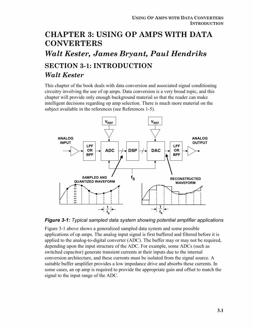
Figure 3-1: Typical sampled data system showing potential amplifier applications Figure 3-1 above shows a generalized sampled data system and some possible applications of op amps. The analog input signal is first buffered and filtered before it is applied to the analog-to-digital converter (ADC). The buffer may or may not be required, depending upon the input structure of the ADC. For example, some ADCs (such as switched capacitor) generate transient currents at their inputs due to the internal conversion architecture, and these currents must be isolated from the signal source. A suitable buffer amplifier provides a low impedance drive and absorbs these currents. In some cases, an op amp is required to provide the appropriate gain and offset to match the signal to the input range of the ADC.
ADC DAC
fS
DSP
SAMPLED ANDQUANTIZED WAVEFORM
RECONSTRUCTEDWAVEFORM
LPFORBPF
LPFORBPF
VREF VREF
ANALOGINPUT
ANALOGOUTPUT
1fS
1fS

OP AMP APPLICATIONS
3.2
Another key component in a sampled data system is the anti-aliasing filter which removes signals that fall outside the Nyquist bandwidth, fs/2. Normally this filter is a lowpass filter, but it can be a bandpass filter in certain undersampling applications. If the op amp buffer is required, it may be located before or after the filter, depending on system considerations. In fact, the filter itself may be an active one, in which case the buffering function can be performed by the actual output amplifier of the filter. More discussions regarding active filters can be found in Chapter 5 of this book. After the signal is buffered and filtered, it is applied to the ADC. The full scale input voltage range of the ADC is generally determined by a voltage reference, VREF. Some ADCs have this function on chip, while others require an external reference. If an external reference is required, its output may require buffering using an appropriate op amp. The reference input to the ADC may be connected to an internal switched capacitor network, causing transient currents to be generated at that node (similar to the analog input of such converters). Therefore some references may require a buffer to isolate these transient currents from the actual reference output. Other references may have internal buffers that are sufficient, and no additional buffering is needed in those cases.
Figure 3-2: Data converter amplifier applications The output of the ADC is then processed digitally by an appropriate processor, shown in the diagram as a digital signal processor (DSP). DSPs are processors that are optimized to perform fast repetitive arithmetic, as required in digital filters or fast Fourier transform (FFT) algorithms. The DSP output then drives a digital-to-analog converter (DAC) which converts the digital signal back into an analog signal. The DAC analog output must be filtered to remove the unwanted image frequencies caused by the sampling process, and further buffering may be required to provide the proper signal amplitude and offset. The output filter is generally placed between the DAC and the buffer amplifier, but their positions can be reversed in certain applications. It is also possible to combine the filtering and buffering function if an active filter is used to condition the DAC output.
Gain settingLevel shiftingBuffering ADC transients from signal sourceBuffering voltage reference outputsBuffering DAC outputsActive anti-aliasing filter before ADCActive anti-imaging filter after DAC

USING OP AMPS WITH DATA CONVERTERS INTRODUCTION
3.3
Trends in Data Converters It is useful to examine a few general trends in data converters, to better understand any associated op amp requirements. Converter performance is first and foremost; and maintaining that performance in a system application is extremely important. In low frequency measurement applications (10Hz bandwidth signals or lower), sigma-delta ADCs with resolutions up to 24 bits are now quite common. These converters generally have automatic or factory calibration features to maintain required gain and offset accuracy. In higher frequency signal processing, ADCs must have wide dynamic range (low distortion and noise), high sampling frequencies, and generally excellent AC specifications. In addition to sheer performance, other characteristics such as low power, single supply operation, low cost, and small surface mount packages also drive the data conversion market. These requirements result in application problems because of reduced signal swings, increased sensitivity to noise, etc. In addition, many data converters are now produced on low-cost foundry CMOS processes which generally make on-chip amplifier design more difficult and therefore less likely to be incorporated on-chip.
Figure 3-3: Some general trends in data converters As has been mentioned previously, the analog input to a CMOS ADC is usually connected directly to a switched-capacitor sample-and-hold (SHA), which generates transient currents that must be buffered from the signal source. On the other hand, data converters fabricated on Bi-CMOS or bipolar processes are more likely to have internal buffering, but generally have higher cost and power than their CMOS counterparts. It should be clear by now that selecting an appropriate op amp for a data converter application is highly dependent on the particular converter under consideration. Generalizations are difficult, but some meaningful guidelines can be followed. The most obvious requirement for a data converter buffer amplifier is that it not degrade the DC or AC performance of the converter. One might assume that a careful reading of the op amp datasheets would assist in the selection process: simply lay the data converter and the op amp datasheets side by side, and compare each critical performance specification. It is true that this method will provide some degree of success, however in order to perform an accurate comparison, the op amp must be specified under the exact operating conditions required by the data converter application. Such factors as gain, gain setting resistor values, source impedance, output load, input and output signal amplitude, input and output common-mode (CM) level, power supply voltage, etc., all affect op amp performance.
Higher sampling rates, higher resolution, higher AC performanceSingle supply operation (e.g., +5V, +3V)Lower powerSmaller input/output signal swingsMaximize usage of low cost foundry CMOS processesSmaller packagesSurface mount technology

OP AMP APPLICATIONS
3.4
It is highly unlikely that even a well written op amp datasheet will provide an exact match to the operating conditions required in the data converter application. Extrapolation of specified performance to fit the exact operating conditions can give erroneous results. Also, the op amp may be subjected to transient currents from the data converter, and the corresponding effects on op amp performance are rarely found on datasheets. Converter datasheets themselves can be a good source for recommended op amps and other application circuits. However this information can become obsolete as newer op amps are introduced after the converter’s initial release. Analog Devices and other op amp manufacturers today have on-line websites featuring parametric search engines, which facilitate part selection (see Reference 1). For instance, the first search might be for minimum power supply voltage, e.g., +3V. The next search might be for bandwidth, and further searches on relevant specifications will narrow the selection of op amps even further. Figure 3-4 below summarizes the selection process.
Figure 3-4: General amplifier selection criteria While not necessarily suitable for the final selection, this process can narrow the search to a manageable number of op amps whose individual datasheets can be retrieved, then reviewed in detail before final selection.
From the discussion thus far, it should be obvious that in order to design a proper interface, an understanding of both op amps and data converters is required. References 2-6 provide background material on data converters. The next section of this chapter addresses key data converter performance specifications without going into the detailed operation of converters themselves. The remainder of the chapter shows a number of specific applications of op amps with various data converters.
The amplifier should not degrade the performance of the ADC/DACAC specifications are usually the most important
NoiseBandwidthDistortion
Selection based on op amp data sheet specifications difficult due to varying conditions in actual application circuit with ADC/DAC:
Power supply voltageSignal range (differential and common-mode)Loading (static and dynamic)Gain
Parametric search engines may be usefulADC/DAC data sheets often recommend op amps (but may not include newly released products)

USING OP AMPS WITH DATA CONVERTERS INTRODUCTION
3.5
REFERENCES: INTRODUCTION 1. ADI website, at http://www.analog.com 2. Walt Kester, Editor, Practical Analog Design Techniques, Analog Devices, 1995, ISBN: 0-916550-
16-8. 3. Walt Kester, Editor, High Speed Design Techniques, Analog Devices, 1996, ISBN: 0-916550-17-6. 4. Chapters 3, 8, Walt Kester, Editor, Practical Design Techniques for Sensor Signal Conditioning,
Analog Devices, 1999, ISBN: 0-916550-20-6. 5. Chapters 2, 3, 4, Walt Kester, Editor, Mixed-Signal and DSP Design Techniques, Analog Devices,
2000, ISBN: 0-916550-23-0. 6. Chapters 4, 5, Walt Kester, Editor, Linear Design Seminar, Analog Devices, 1995, ISBN: 0-916550-
15-X.

OP AMP APPLICATIONS
3.6
NOTES:

USING OP AMPS WITH DATA CONVERTERS ADC/DAC SPECIFICATIONS
3.7
SECTION 3-2: ADC/DAC SPECIFICATIONS Walt Kester
ADC and DAC Static Transfer Functions and DC Errors The most important thing to remember about both DACs and ADCs is that either the input or output is digital, and therefore the signal is quantized. That is, an N-bit word represents one of 2N possible states, and therefore an N-bit DAC (with a fixed reference) can have only 2N possible analog outputs, and an N-bit ADC can have only 2N possible digital outputs. The analog signals will generally be voltages or currents. The resolution of data converters may be expressed in several different ways: the weight of the Least Significant Bit (LSB), parts per million of full scale (ppm FS), millivolts (mV), etc. It is common that different devices (even from the same manufacturer) will be specified differently, so converter users must learn to translate between the different types of specifications if they are to compare devices successfully. The size of the least significant bit for various resolutions is shown in Figure 3-5 below.
Figure 3-5: Quantization: the size of a least significant bit (LSB) As noted above (and obvious from this table), the LSB scaling for a given converter resolution can be expressed in various ways. While it is convenient to relate this to a full scale of 10V, as in the figure, other full scale levels can be easily extrapolated. Before we can consider op amp applications with data converters, it is necessary to consider the performance to be expected, and the specifications that are important when operating with data converters. The following sections will consider the definition of errors and specifications used for data converters.
RESOLUTIONN
2-bit
4-bit
6-bit
8-bit
10-bit
12-bit
14-bit
16-bit
18-bit
20-bit
22-bit
24-bit
2N
4
16
64
256
1,024
4,096
16,384
65,536
262,144
1,048,576
4,194,304
16,777,216
VOLTAGE(10V FS)
2.5 V
625 mV
156 mV
39.1 mV
9.77 mV (10 mV)
2.44 mV
610 µV
153 µV
38 µV
9.54 µV (10 µV)
2.38 µV596 nV*
ppm FS
250,000
62,500
15,625
3,906
977
244
61
15
4
1
0.24
0.06
% FS
25
6.25
1.56
0.39
0.098
0.024
0.0061
0.0015
0.0004
0.0001
0.000024
0.000006
dB FS
-12
-24
-36
-48
-60
-72
-84
-96
-108
-120
-132
-144
*600nV is the Johnson Noise in a 10kHz BW of a 2.2kΩ Resistor @ 25°C
Remember: 10-bits and 10V FS yields an LSB of 10mV, 1000ppm, or 0.1%.All other values may be calculated by powers of 2.

OP AMP APPLICATIONS
3.8
The first applications of data converters were in measurement and control, where the exact timing of the conversion was usually unimportant, and the data rate was slow. In such applications, the DC specifications of converters are important, but timing and AC specifications are not. Today many, if not most, converters are used in sampling and reconstruction systems where AC specifications are critical (and DC ones may not be).
Figure 3-6: DAC transfer functions Figure 3-6 above shows the transfer characteristics for a 3-bit unipolar ideal and non-ideal DAC. In a DAC, both the input and output are quantized, and the graph consists of eight points— while it is reasonable to discuss a line through these points, it is critical to remember that the actual transfer characteristic is not a line, but a series of discrete points. Similarly, Figure 3-7 below shows the transfer characteristics for a 3-bit unipolar ideal and non-ideal ADC. Note that the input to an ADC is analog and is therefore not quantized, but its output is quantized.
Figure 3-7: ADC transfer functions The ADC transfer characteristic therefore consists of eight horizontal steps (when considering the offset, gain and linearity of an ADC we consider the line joining the midpoints of these steps).
DIGITAL INPUT
ANALOGOUTPUT
FS
000 001 010 011 100 101 110 111
DIGITAL INPUT
FS
000 001 010 011 100 101 110 111
NON-MONOTONIC
IDEAL NON-IDEAL
ANALOG INPUT
DIGITALOUTPUT
FS000
001
010
011
100
101
110
111
QUANTIZATIONUNCERTAINTY
ANALOG INPUT FS000
001
010
011
100
101
110
111
MISSING CODE
IDEAL NON-IDEAL
USING OP AMPS WITH DATA CONVERTERS ADC/DAC SPECIFICATIONS
3.9
The (ideal) ADC transitions take place at ½ LSB above zero, and thereafter every LSB, until 1½ LSB below analog full scale. Since the analog input to an ADC can take any value, but the digital output is quantized, there may be a difference of up to ½ LSB between the actual analog input and the exact value of the digital output. This is known as the quantization error or quantization uncertainty as shown in Figure 3-7. In AC (sampling) applications this quantization error gives rise to quantization noise which will be discussed shortly. The integral linearity error of a converter is analogous to the linearity error of an amplifier, and is defined as the maximum deviation of the actual transfer characteristic of the converter from a straight line. It is generally expressed as a percentage of full scale (but may be given in LSBs). There are two common ways of choosing the straight line: end point and best straight line. In the end point system, the deviation is measured from the straight line through the origin and the full scale point (after gain adjustment). This is the most useful integral linearity measurement for measurement and control applications of data converters (since error budgets depend on deviation from the ideal transfer characteristic, not from some arbitrary "best fit"), and is the one normally adopted by Analog Devices, Inc. The best straight line, however, does give a better prediction of distortion in AC applications, and also gives a lower value of "linearity error" on a datasheet. The best fit straight line is drawn through the transfer characteristic of the device using standard curve fitting techniques, and the maximum deviation is measured from this line. In general, the integral linearity error measured in this way is only 50% of the value measured by end point methods. This makes the method good for producing impressive datasheets, but it is less useful for error budget analysis. For AC applications, it is even better to specify distortion than DC linearity, so it is rarely necessary to use the best straight line method to define converter linearity. The other type of converter non-linearity is differential non-linearity (DNL). This relates to the linearity of the code transitions of the converter. In the ideal case, a change of 1 LSB in digital code corresponds to a change of exactly 1 LSB of analog signal. In a DAC, a change of 1 LSB in digital code produces exactly 1 LSB change of analog output, while in an ADC there should be exactly 1 LSB change of analog input to move from one digital transition to the next. Where the change in analog signal corresponding to 1 LSB digital change is more or less than 1 LSB, there is said to be a DNL error. The DNL error of a converter is normally defined as the maximum value of DNL to be found at any transition. If the DNL of a DAC is less than –1 LSB at any transition (Figure 3-6, again), the DAC is non-monotonic; i.e., its transfer characteristic contains one or more localized maxima or minima. A DNL greater than +1 LSB does not cause non-monotonicity, but is still undesirable. In many DAC applications (especially closed-loop systems where non-monotonicity can change negative feedback to positive feedback), it is critically important that DACs are monotonic. DAC monotonicity is often explicitly specified on datasheets,

OP AMP APPLICATIONS
3.10
but if the DNL is guaranteed to be less than 1 LSB (i.e., |DNL| ≤ 1LSB) then the device must be monotonic, even without an explicit guarantee. ADCs can be non-monotonic, but a more common result of excess DNL in ADCs is missing codes (Figure 3-7, again). Missing codes (or non-monotonicity) in an ADC are as objectionable as non-monotonicity in a DAC. Again, they result from DNL > 1 LSB. Quantization Noise in Data Converters The only errors (DC or AC) associated with an ideal N-bit ADC are those related to the sampling and quantization processes. The maximum error an ideal ADC makes when digitizing a DC input signal is ±1/2LSB. Any AC signal applied to an ideal N-bit ADC will produce quantization noise whose rms value (measured over the Nyquist bandwidth, DC to fs/2) is approximately equal to the weight of the least significant bit (LSB), q, divided by √12. This assumes that the signal is at least a few LSBs in amplitude so that the ADC output always changes state. The quantization error signal from a linear ramp input is approximated as a sawtooth waveform with a peak-to-peak amplitude equal to q, and its rms value is therefore q/√12 (see Figure 3-8 below).
Figure 3-8: Ideal N-bit ADC quantization noise It can be shown that the ratio of the rms value of a full scale sinewave to the rms value of the quantization noise (expressed in dB) is:
SNR = 6.02N + 1.76dB, Eq. 3-1 where N is the number of bits in the ideal ADC. Note— this equation is only valid if the noise is measured over the entire Nyquist bandwidth from DC to fs/2. If the signal bandwidth, BW, is less than fs/2, then the SNR within the signal bandwidth BW is increased because the amount of quantization noise within the signal bandwidth is less.
DIGITALCODEOUTPUT
ANALOGINPUT
ERRORq = 1LSB
SNR = 6.02N + 1.76dB + 10log FOR FS SINEWAVEfs2•BW
RMS ERROR = q/√12

USING OP AMPS WITH DATA CONVERTERS ADC/DAC SPECIFICATIONS
3.11
The correct expression for this condition is given by:
SNR N dBfsBW
= + +⋅
6 02 176 102
. . log . Eq. 3-2
The above equation reflects the condition called oversampling, where the sampling frequency is higher than twice the signal bandwidth. The correction term is often called processing gain. Notice that for a given signal bandwidth, doubling the sampling frequency increases the SNR by 3dB. ADC Input-Referred Noise The internal circuits of an ADC produce a certain amount of wideband rms noise due to thermal and kT/C effects. This noise is present even for DC input signals, and accounts for the fact that the output of most wideband (or high resolution) ADCs is a distribution of codes, centered around the nominal DC input value, as is shown in Figure 3-9 below.
Figure 3-9: Effect of ADC input-referred noise on "grounded input" histogram To measure its value, the input of the ADC is grounded, and a large number of output samples are collected and plotted as a histogram (sometimes referred to as a grounded-input histogram). Since the noise is approximately Gaussian, the standard deviation (σ) of the histogram is easily calculated, corresponding to the effective input rms noise. It is common practice to express this rms noise in terms of LSBs, although it can be expressed as an rms voltage.
n n+1 n+2 n+3 n+4n–1n–2n–3n–4
NUMBER OFOCCURRENCES
RMS NOISE (σ)
P-P INPUT NOISE
≈ 6.6 × RMS NOISE
OUTPUT CODE

OP AMP APPLICATIONS
3.12
Calculating Op Amp Output Noise and Comparing it with ADC Input-Referred Noise In precision measurement applications utilizing 16- to 24-bit sigma-delta ADCs operating on low frequency (<20Hz, e.g.) signals, it is generally undesirable to use a drive amplifier in front of the ADC because of the increased noise due to the amplifier itself. If an op amp is required, however, the op amp output 1/f noise should be compared to the input-referred ADC noise. The 1/f noise is usually specified as a peak-to-peak value measured over the 0.1Hz to 10Hz bandwidth and referred to the op amp input (see Chapter 1 of this book). Op amps such as the OP177 and the AD707 (input voltage noise 350nV p-p) or the AD797 (input voltage noise 50nV p-p) are appropriate for high resolution measurement applications if required.
Figure 3-10: Op amp noise model for a first-order circuit with resistive feedback The general model for calculating the referred-to-input (RTI) or referred-to-output (RTO) noise of an op amp is shown in Figure 3-10 above. This model shows all possible noise sources. The results using this model are relatively accurate, provided there is less than 1dB gain peaking in the closed loop frequency response. For higher frequency applications, 1/f noise can be neglected, because the dominant contributor is white noise. An example of a practical noise calculation is shown in Figure 3-11 (opposite). In this circuit, a wideband, low distortion amplifier (AD9632) drives a 12-bit, 25MSPS ADC (AD9225). The input voltage noise spectral density of the AD9632 (4.3nV/√Hz) dominates the op amp noise because of the low gain and the low values of the external feedback resistors. The noise at the output of the AD9632 is obtained by multiplying the input voltage noise spectral density by the noise gain of 2. To obtain the rms noise, the noise spectral density is multiplied by the equivalent noise bandwidth of 50MHz which is set by the single-pole lowpass filter placed between the op amp and the ADC input.
CLOSEDLOOP BW
= fCL
–
+
VN∼
R2
R1
R3
IN–
IN+
VOUT
NOISE GAIN =
1 + R2R1
NG =∼∼
∼∼
∼∼VN,R1
VN,R3
VN,R2
RTI NOISE =
VN2 + 4kTR3 + 4kTR1 R2
R1+R2
2R2
R1+R2
2
+ IN+2R32 + IN–
2 R1•R2R1+R2
2+ 4kTR2 R1
R1+R2
2R1
R1+R2
2BW •
RTO NOISE = NG • RTI NOISE
4kTR1
4kTR3
4kTR2
A
B
GAIN FROM "A" TO OUTPUT
GAIN FROM"B" TO OUTPUT
= – R2R1
=
BW = 1.57 fCL

USING OP AMPS WITH DATA CONVERTERS ADC/DAC SPECIFICATIONS
3.13
Note that the closed-loop bandwidth of the AD9632 is 250MHz, and the input bandwidth of the AD9225 is 105MHz. With no filter, the output noise of the AD9632 would be integrated over the full 105MHz ADC input bandwidth. However, the sampling frequency of the ADC is 25MSPS, thereby implying that signals above 12.5MHz are not of interest, assuming Nyquist operation (as opposed to undersampling applications where the input signal can be greater than the Nyquist frequency, fs/2). The addition of this simple filter significantly reduces noise effects.
Figure 3-11: Noise calculations for the AD9632 op amp driving the AD9225 12-bit, 25MSPS ADC
The noise at the output of the lowpass filter is calculated as approximately 61µV rms which is less than half the effective input noise of the AD9225, 166µV rms. Without the filter, the noise from the op amp would be about 110µV rms (integrating over the full equivalent ADC input noise bandwidth of 1.57×10⁵MHz = 165MHz).
Figure 3-12: Proper positioning of the antialiasing filter will reduce the effects of op amp noise
This serves to illustrate the general concept shown in Figure 3-12 above. In most high speed system applications a passive antialiasing filter (either lowpass for baseband sampling, or bandpass for undersampling) is required, and placing this filter between the op amp and the ADC will serve to reduce the noise due to the op amp.
fFILTER
AMP
AMP
LPFORBPF
LPFORBPF
ADC
ADC
fFILTERfs
fs
fCL
fCL
AMP NOISE INTEGRATEDOVER fCL OR fADC,WHICHEVER IS LESS
AMP NOISE INTEGRATEDOVER FILTER BW, fFILTERfADC
fADC
IN GENERAL, fFILTER < << fADC < fCLfs2
AD922512-bit ADC
fs = 25MSPS
VniVni
AD963275Ω
103Ω
274Ω
+
-274Ω
VREF
VINA 50Ω
1.0kΩ
100pF
0.1uF
Noise Bandwidth = 1.57 •1
2π RC = 50MHz
AD9632 OP AMP SPECIFICATIONS
Input Voltage Noise = 4.3nV/√ HzClosed-Loop Bandwidth = 250MHz
AD9225 ADC SPECIFICATIONS
Effective Input Noise = 166µV rmsSmall Signal Input BW = 105MHz
AD9632 Output Noise Spectral Density = 2 • 4.3nV/√ Hz = 8.6nV/√ Hz
Vni = 8.6nV/√ Hz • 50MHz = 61µV rms Vni = 8.6nV/√ Hz • 50MHz = 61µV rms
R =
C =

OP AMP APPLICATIONS
3.14
Quantifying and Measuring Converter Dynamic Performance There are various ways to characterize the AC performance of ADCs. In the early years of ADC technology (over 30 years ago) there was little standardization with respect to AC specifications, and measurement equipment and techniques were not well understood or available. Over nearly a 30 year period, manufacturers and customers have learned more about measuring the dynamic performance of converters, and the specifications shown in Figure 3-13 below represent the most popular ones used today.
Figure 3-13: Quantifying ADC dynamic performance Practically all the specifications represent the converter’s performance in the frequency domain, and all are related to noise and distortion in one manner or another.
Figure 3-14: Measuring ADC / DAC dynamic performance ADC outputs are analyzed using fast Fourier transform (FFT) techniques, and DAC outputs are analyzed using conventional analog spectrum analyzers, as shown in Figure 3-14 above. In the case of an ADC, the input signal is an analog sinewave, and in the case of a DAC, the input is a digital sinewave generated by a direct digital synthesis (DDS) system.
SIGNALGEN. ADC
BUFFERMEMORY
MSAMPLES
DSPM-POINT
FFT
DDS DACANALOG
SPECTRUMANALYZER
fs2
Resolution= fs / M
f
Signal-to-Noise-and-Distortion Ratio (SINAD, or S/N +D)Effective Number of Bits (ENOB)Signal-to-Noise Ratio (SNR)Analog Bandwidth (Full-Power, Small-Signal)Harmonic DistortionWorst HarmonicTotal Harmonic Distortion (THD)Total Harmonic Distortion Plus Noise (THD + N)Spurious Free Dynamic Range (SFDR)Two-Tone Intermodulation DistortionMulti-tone Intermodulation Distortion

USING OP AMPS WITH DATA CONVERTERS ADC/DAC SPECIFICATIONS
3.15
Signal-to-Noise-and-Distortion Ratio (SINAD), Signal-to-Noise Ratio (SNR), and Effective Number of Bits (ENOB) SINAD and SNR deserve careful attention (see Figure 3-15 below), because there is still some variation between ADC manufacturers as to their precise meaning. Signal-to-noise-and Distortion (SINAD, or S/N+D) is the ratio of the rms signal amplitude to the mean value of the root-sum-square (RSS) of all other spectral components, including harmonics, but excluding DC. SINAD is a good indication of the overall dynamic performance of an ADC as a function of input frequency, because it includes all components which make up noise (including thermal noise) and distortion. It is often plotted for various input amplitudes. SINAD is equal to THD+N if the bandwidth for the noise measurement is the same.
Figure 3-15: SINAD, ENOB, and SNR The SINAD plot shows where the AC performance of the ADC degrades due to high-frequency distortion, and is usually plotted for frequencies well above the Nyquist frequency so that performance in undersampling applications can be evaluated. SINAD is often converted to effective-number-of-bits (ENOB) using the relationship for the theoretical SNR of an ideal N-bit ADC: SNR = 6.02N + 1.76dB. The equation is solved for N, and the value of SINAD is substituted for SNR:
ENOBSINAD dB
=− 176
6 02.
.. Eq. 3-3
Signal-to-noise ratio (SNR, or SNR-without-harmonics) is calculated the same as SINAD except that the signal harmonics are excluded from the calculation, leaving only the noise terms. In practice, it is only necessary to exclude the first 5 harmonics since they dominate. The SNR plot will degrade at high frequencies, but not as rapidly as SINAD because of the exclusion of the harmonic terms.
SINAD (Signal-to-Noise-and-Distortion Ratio):The ratio of the rms signal amplitude to the mean value of the root-sum-squares (RSS) of all other spectral components, including harmonics, but excluding DC.
ENOB (Effective Number of Bits):
ENOB =
SNR (Signal-to-Noise Ratio, or Signal-to-Noise Ratio Without Harmonics:
The ratio of the rms signal amplitude to the mean value of the root-sum-squares (RSS) of all other spectral components, excluding the first 5 harmonics and DC
SINAD – 1.76dB6.02
SINAD – 1.76dB6.02

OP AMP APPLICATIONS
3.16
Many current ADC datasheets somewhat loosely refer to SINAD as SNR, so the design engineer must be careful when interpreting these specifications.
Figure 3-16: AD9220 12-bit, 10MSPS ADC SINAD and ENOB for various input signal levels
A SINAD/ENOB plot for the AD9220 12-bit, 10MSPS ADC is shown in Figure 3-16. Analog Bandwidth The analog bandwidth of an ADC is that frequency at which the spectral output of the fundamental swept frequency (as determined by the FFT analysis) is reduced by 3dB. It may be specified for either a small signal bandwidth (SSBW), or a full scale signal (FPBW- full power bandwidth), so there can be a wide variation in specifications between manufacturers.
Figure 3-17: ADC Gain (bandwidth) and ENOB versus frequency shows importance of ENOB specification
Like an amplifier, the analog bandwidth specification of a converter does not imply that the ADC maintains good distortion performance up to its bandwidth frequency. In fact,
13.0
12.2
11.3
10.5
9.7
8.8
8.0
7.2
6.3
ENOBSINAD(dB)
ANALOG INPUT FREQUENCY (MHz)
ADC INPUT FREQUENCY (Hz)
ENOB
GAIN (FS INPUT)
ENOB (FS INPUT)
ENOB (-20dB INPUT)
FPBW = 1MHz
10 100 1k 10k 100k 1M 10M
GAIN

USING OP AMPS WITH DATA CONVERTERS ADC/DAC SPECIFICATIONS
3.17
the SINAD (or ENOB) of most ADCs will begin to degrade considerably before the input frequency approaches the actual 3dB bandwidth frequency. Figure 3-17 (opposite) shows ENOB and full scale frequency response of an ADC with a FPBW of 1MHz, however, the ENOB begins to drop rapidly above 100kHz. Harmonic Distortion, Worst Harmonic, Total Harmonic Distortion (THD), Total Harmonic Distortion Plus Noise (THD + N) There are a number of ways to quantify the distortion of an ADC. An FFT analysis can be used to measure the amplitude of the various harmonics of a signal. The harmonics of the input signal can be distinguished from other distortion products by their location in the frequency spectrum. Figure 3-18 below shows a 7MHz input signal sampled at 20MSPS and the location of the first 9 harmonics. Aliased harmonics of fa fall at frequencies equal to |±Kfs±nfa|, where n is the order of the harmonic, and K = 0, 1, 2, 3,.... The second and third harmonics are generally the only ones specified on a datasheet because they tend to be the largest, although some datasheets may specify the value of the worst harmonic.
Figure 3-18: Location of harmonic distortion products: Input signal = 7MHz, sampling rate = 20MSPS
Harmonic distortion is normally specified in dBc (decibels below carrier), although in audio applications it may be specified as a percentage. Harmonic distortion is generally specified with an input signal near full scale (generally 0.5 to 1dB below full scale to avoid clipping), but it can be specified at any level. For signals much lower than full scale, other distortion products due to the DNL of the converter (not direct harmonics) may limit performance. Total harmonic distortion (THD) is the ratio of the rms value of the fundamental signal to the mean value of the root-sum-square of its harmonics (generally, only the first 5 are significant). THD of an ADC is also generally specified with the input signal close to full scale, although it can be specified at any level.
RELATIVEAMPLITUDE
FREQUENCY (MHz)
fa
1 2 3 4 5 6 7 8 9 10
3
69 8 5 7
HARMONICS AT: |±Kfs±nfa|n = ORDER OF HARMONIC, K = 0, 1, 2, 3, . . .
2
4
= 7MHz
fs = 20MSPS

OP AMP APPLICATIONS
3.18
Total harmonic distortion plus noise (THD+ N) is the ratio of the rms value of the fundamental signal to the mean value of the root-sum-square of its harmonics plus all noise components (excluding DC). The bandwidth over which the noise is measured must be specified. In the case of an FFT, the bandwidth is DC to fs/2. (If the bandwidth of the measurement is DC to fs/2, THD+N is equal to SINAD. Spurious Free Dynamic Range (SFDR) Probably the most significant specification for an ADC used in a communications application is its spurious free dynamic range (SFDR). The SFDR specification is to ADCs what the third order intercept specification is to mixers and LNAs.
Figure 3-19: Spurious free dynamic range (SFDR) SFDR of an ADC is defined as the ratio of the rms signal amplitude to the rms value of the peak spurious spectral content (measured over the entire first Nyquist zone, DC to fs/2). SFDR is generally plotted as a function of signal amplitude and may be expressed relative to the signal amplitude (dBc) or the ADC full scale (dBFS) as shown in Figure 3-19 above. For a signal near full scale, the peak spectral spur is generally determined by one of the first few harmonics of the fundamental. However, as the signal falls several dB below full scale, other spurs generally occur which are not direct harmonics of the input signal. This is because of the differential non-linearity of the ADC transfer function as discussed earlier. Therefore, SFDR considers all sources of distortion, regardless of their origin.
FULL SCALE (FS)
dBSFDR (dBc)
fs2
INPUT SIGNAL LEVEL (CARRIER)
WORST SPUR LEVEL
SFDR (dBFS)
FREQUENCY

USING OP AMPS WITH DATA CONVERTERS ADC/DAC SPECIFICATIONS
3.19
Two Tone Intermodulation Distortion (IMD) Two tone IMD is measured by applying two spectrally pure sinewaves to the ADC at frequencies f1 and f2, usually relatively close together. The amplitude of each tone is set slightly more than 6dB below full scale so that the ADC does not clip when the two tones add in-phase. Second and third-order product locations are shown in Figure 3-20 below. Notice that the second-order products fall at frequencies which can be removed by digital filters. However, the third-order products 2f2–f1 and 2f1–f2 are close to the original signals, and are almost impossible to filter. Unless otherwise specified, two-tone IMD refers to these third-order products. The value of the IMD product is expressed in dBc relative to the value of either of the two original tones, and not to their sum.
Figure 3-20: Second and third-order intermodulation products for f1 = 5MHz, f2 = 6MHz
Note, however, that if the two tones are close to fs/4, then the aliased third harmonics of the fundamentals can make the identification of the actual 2f2–f1 and 2f1–f2 products difficult. This is because the third harmonic of fs/4 is 3fs/4, and the alias occurs at fs – 3fs/4 = fs/4. Similarly, if the two tones are close to fs/3, the aliased second harmonics may interfere with the measurement. The same reasoning applies here; the second harmonic of fs/3 is 2 fs/3, and its alias occurs at fs – 2 fs/3 = fs/3. The concept of second and third-order intercept points is not valid for an ADC, because the distortion products don't vary predictably (as a function of signal amplitude). The ADC doesn't gradually begin to compress signals approaching full scale (there is no 1dB compression point); it acts as a hard limiter as soon as the signal exceeds the input range, producing extreme distortion due to clipping. Conversely, for signals much below full scale, the distortion floor remains relatively constant and is independent of signal level. Multi-tone SFDR is often measured in communications applications. The larger number of tones more closely simulates the wideband frequency spectrum of cellular telephone systems such as AMPS or GSM. High SFDR increases the receiver’s ability to capture small signals in the presence of large ones, and prevent the small signals from being masked by the intermodulation products of the larger ones.
FREQUENCY: MHz
2 = SECOND ORDER IMD PRODUCTS
3 = THIRD ORDER IMD PRODUCTS
NOTE: f1 = 5MHz, f2 = 6MHz
f2 - f1
2f1 - f2 2f2 - f1
f1 f2
2f1 2f2f2 + f1
2f1 + f2
3f1 2f2 + f1
3f2
2
3 3
2
33
1 4 5 6 7 10 11 12 15 16 17 18

OP AMP APPLICATIONS
3.20
REFERENCES: ADC/DAC SPECIFICATIONS 1. Walt Kester, Editor, Practical Analog Design Techniques, Analog Devices, 1995, ISBN: 0-916550-
16-8. 2. Walt Kester, Editor, High Speed Design Techniques, Analog Devices, 1996, ISBN: 0-916550-17-6. 3. Chapters 3, 8, Walt Kester, Editor, Practical Design Techniques for Sensor Signal Conditioning,
Analog Devices, 1999, ISBN: 0-916550-20-6. 4. Chapters 2, 3, 4, Walt Kester, Editor, Mixed-Signal and DSP Design Techniques, Analog Devices,
2000, ISBN: 0-916550-23-0. 5. Chapters 4, 5, Walt Kester, Editor, Linear Design Seminar, Analog Devices, 1995, ISBN: 0-916550-
15-X.

USING OP AMPS WITH DATA CONVERTERS DRIVING ADC INPUTS
3.21
SECTION 3-3: DRIVING ADC INPUTS Walt Kester, Paul Hendriks
Introduction Op amps are often used as drivers for ADCs to provide the gain and level shifting required for the input signal to match the input range of the ADC. An op amp may be required because of the antialiasing filter impedance matching requirements. In some cases, the antialiasing filter may be an active filter and include op amps as part of the filter itself. Some ADCs also generate transient currents on their inputs due to the conversion process, and these must be isolated from the signal source with an op amp. This section examines these and other issues involved in driving high performance ADCs. To begin with, one shouldn't necessarily assume that a driver op amp is always required. Some converters have relatively benign inputs and are designed to interface directly to the signal source. There is practically no industry standardization regarding ADC input structures, and therefore each ADC must be carefully examined on its own merits before designing the input interface circuitry. In some applications, transformer drive may be preferable.
Figure 3-21: General op amp requirements in ADC driver applications Assuming an op amp is required for one reason or another, the task of its selection is a critical one and not at all straightforward. Figure 3-21 above lists a few of the constraints and variables. The most important requirement is that the op amp should not significantly degrade the overall DC or AC performance of the ADC. At first glance, it would appear that a careful comparison of an op amp datasheet with the ADC datasheet would allow an appropriate choice. However, this is rarely the case. The problem is that the op amp performance specifications must be known for the exact circuit configuration used in the ADC driver circuit. Even a very complete datasheet is unlikely to provide all information required, due to the wide range of possible variables.
Minimize degradation of ADC / DAC performance specificationsFast settling to ADC/DAC transientHigh bandwidthLow noiseLow distortionLow power
Note: Op amp performance must be measured under identical conditions as encountered in ADC / DAC application
Gain setting resistorsInput source impedance, output load impedanceInput / output signal voltage rangeInput signal frequencyInput / output common-mode levelPower supply voltage (single or dual supply)Transient loading

OP AMP APPLICATIONS
3.22
Although the op amp and ADC datasheets should definitely be used as a guide in the selection process, it is unlikely that the overall performance of the op amp/ADC combination can be predicted accurately without actually prototyping the circuit, especially in high performance applications. Various tested application circuits are often recommended on either the op amp or the ADC datasheet, but these can become obsolete quickly as new op amps are released. In most cases, however, the ADC datasheet application section should be used as the primary source for tested interfaces. Op Amp Specifications Key to ADC Applications The two most popular applications for ADCs today are in either precision high-resolution measurements or in low distortion high speed systems. Precision measurement applications require ADCs of at least 16 bits of resolution, and sometimes up to 24 bits. Op amps used with these ADCs must be low noise and have excellent DC characteristics. In fact, high resolution measurement ADCs are often designed to interface directly with the transducer, eliminating the need for an op amp entirely.
Figure 3-22: Key op amp specifications If op amps are required, it is generally relatively straightforward to select one based on well-understood DC specifications, as listed in Figure 3-22 above. It is much more difficult to provide a complete set of op amp AC specifications because they are highly dependent upon the application circuit. For example, Figure 3-23 (opposite) shows some key specifications taken from the table of specifications on the datasheet for the AD8057/AD8058 high speed, low distortion op amp (see Reference 1). Note that the specifications depend on the supply voltage, the signal level, output loading, etc. It should also be emphasized that it is customary to provide only typical AC specifications (as opposed to maximum and minimum values) for most op amps. In
DCOffset, offset driftInput bias currentOpen loop gainIntegral linearity1/f noise (voltage and current)
AC (Highly application dependent!)Wideband noise (voltage and current)Small and Large Signal BandwidthHarmonic DistortionTotal Harmonic Distortion (THD)Total Harmonic Distortion + Noise (THD + N)Spurious Free Dynamic Range (SFDR)Third Order Intermodulation DistortionThird Order Intercept Point

USING OP AMPS WITH DATA CONVERTERS DRIVING ADC INPUTS
3.23
addition, there are restrictions on the input and output CM signal ranges, which are especially important when operating on low voltage dual (or single) supplies.
Figure 3-23: AD8057/AD8058 op amp key AC specifications, G = +1 Most op amp datasheets contain a section that provides supplemental performance data for various other conditions not explicitly specified in the primary specification tables. For instance, Figure 3-24 below shows the AD8057/AD8058 distortion as a function of frequency for G = +1 and VS = ±5V. Unless it is otherwise specified, the data represented by these curves should be considered typical (it is usually marked as such).
Figure 3-24: AD8057/AD8058 op amp distortion versus frequency G = +1, RL = 150Ω, VS = ±5V
Note however that the data in both Fig. 3-24 (and also the following Figure 3-25) is given for a DC load of 150Ω. This is a load presented to the op amp in the popular application of driving a source and load-terminated 75Ω cable. Distortion performance is generally better with lighter DC loads, such as 500Ω - 1000Ω (more typical of many ADC inputs), and this data may or may not be found on the datasheet.
Input Common Mode Voltage RangeOutput Common Mode Voltage Range
Input Voltage NoiseSmall Signal Bandwidth
THD @ 5MHz, VO = 2V p-p, RL = 1kΩTHD @ 20MHz, VO = 2V p-p, RL = 1kΩ
VS = ±5V VS = +5V
–4.0V to +4.0V–4.0V to +4.0V
7nV/√Hz325MHz
– 85dBc– 62dBc
+0.9V to +3.4V+0.9V to +4.1V
7nV/√Hz300MHz
– 75dBc– 54dBc

OP AMP APPLICATIONS
3.24
On the other hand, Figure 3-25 below shows distortion as a function of output signal level for a frequencies of 5MHz and 20MHz.
Figure 3-25: AD8057/AD8058 op amp distortion versus output voltage G = +1, RL = 150Ω, VS = ±5V
Whether or not specifications such as those just described are complete enough to select an op amp for an ADC driver application depends upon the ability to match op amp specifications to the actually required ADC operating conditions. In many cases, these comparisons will at least narrow the op amp selection process. The following sections will examine a number of specific driver circuit examples using various types of ADCs, ranging from high resolution measurement to high-speed, low distortion applications. Driving High Resolution Sigma-Delta Measurement ADCs The AD77XX family of ADCs is optimized for high resolution (16–24 bits) low frequency transducer measurement applications. Details of operation can be found in Reference 2, and general characteristics of the family are listed in Figure 3-26 below.
Figure 3-26: High resolution low frequency measurement ADCs Some members of this family, such as the AD7730, have a high impedance input buffer which isolates the analog inputs from switching transients generated in the front-end programmable gain amplifier (PGA) and the sigma-delta modulator. Therefore, no special
THD @
THD @
Resolution: 16 - 24 bitsInput signal bandwidth: <60HzEffective sampling rate: <100HzGenerally Sigma-Delta architectureDesigned to interface directly to sensors (< 1 kΩ) such as bridges with no external buffer amplifier (e.g., AD77XX - series)
On-chip PGA and high resolution ADC eliminates the need for external amplifier
If buffer is used, it should be precision low noise (especially 1/f noise)OP177AD707AD797

USING OP AMPS WITH DATA CONVERTERS DRIVING ADC INPUTS
3.25
precautions are required in driving the analog inputs. Other members of the AD77XX family, however, either do not have the input buffer, or if one is included on-chip, it can be switched either in or out under program control. Bypassing the buffer offers a slight improvement in noise performance. The equivalent input circuit of the AD77XX family without an input buffer is shown below in Figure 3-27. The input switch alternates between the 10pF sampling capacitor and ground. The 7kΩ internal resistance, RINT, is the on-resistance of the input multiplexer. The switching frequency is dependent on the frequency of the input clock and also the internal PGA gain. If the converter is working to an accuracy of 20-bits, the 10pF internal capacitor, CINT, must charge to 20-bit accuracy during the time the switch connects the capacitor to the input. This interval is one-half the period of the switching signal (it has a 50% duty cycle). The input RC time constant due to the 7kΩ resistor and the 10pF sampling capacitor is 70ns. If the charge is to achieve 20-bit accuracy, the capacitor must charge for at least 14 time constants, or 980ns. Any external resistance in series with the input will increase this time constant.
Figure 3-27: Driving unbuffered AD77XX-series Σ∆ ADC inputs There are tables on the datasheets for the various AD77XX ADCs, which give the maximum allowable values of REXT in order to maintain a given level of accuracy. These tables should be consulted if the external source resistance is more than a few kΩ. Note that for instances where an external op amp buffer is found to be required with this type of converter, guidelines exist for best overall performance. This amplifier should be a precision low-noise bipolar-input type, such as the OP177, AD707, or the AD797.
HIGHIMPEDANCE
> 1GΩ
SWITCHING FREQDEPENDS ON fCLKIN AND GAIN
CINT10pF TYP
REXT RINT
7kΩ
~
REXT Increases CINT Charge Time and May Result in Gain Error
Charge Time Dependent on the Input Sampling Rate and InternalPGA Gain Setting
Refer to Specific Data Sheet for Allowable Values of REXT toMaintain Desired Accuracy
Some AD77XX-Series ADCs Have Internal Buffering Which IsolatesInput from Switching Circuits
AD77XX-Series(WITHOUT BUFFER)
VSOURCE
OP AMP APPLICATIONS
3.26
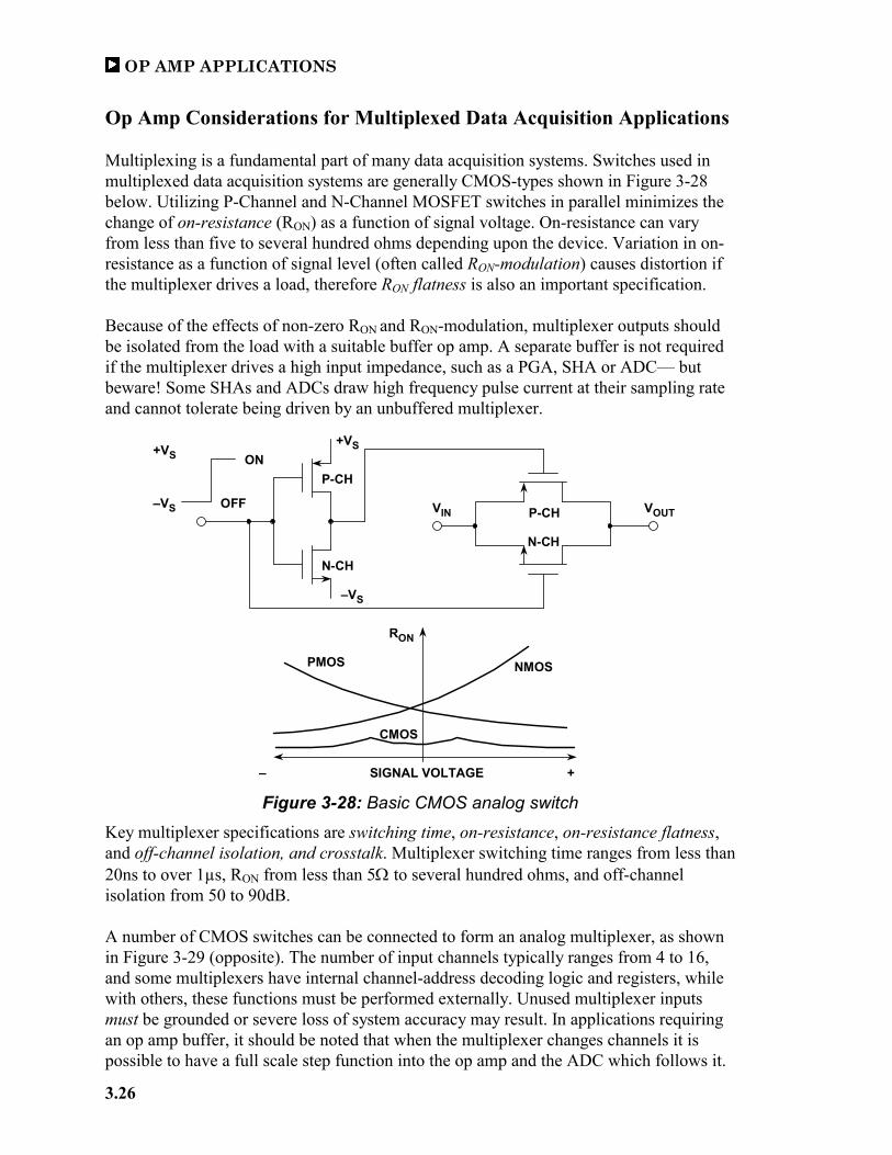
Op Amp Considerations for Multiplexed Data Acquisition Applications Multiplexing is a fundamental part of many data acquisition systems. Switches used in multiplexed data acquisition systems are generally CMOS-types shown in Figure 3-28 below. Utilizing P-Channel and N-Channel MOSFET switches in parallel minimizes the change of on-resistance (RON) as a function of signal voltage. On-resistance can vary from less than five to several hundred ohms depending upon the device. Variation in on-resistance as a function of signal level (often called RON-modulation) causes distortion if the multiplexer drives a load, therefore RON flatness is also an important specification. Because of the effects of non-zero RON and RON-modulation, multiplexer outputs should be isolated from the load with a suitable buffer op amp. A separate buffer is not required if the multiplexer drives a high input impedance, such as a PGA, SHA or ADC— but beware! Some SHAs and ADCs draw high frequency pulse current at their sampling rate and cannot tolerate being driven by an unbuffered multiplexer.
Figure 3-28: Basic CMOS analog switch Key multiplexer specifications are switching time, on-resistance, on-resistance flatness, and off-channel isolation, and crosstalk. Multiplexer switching time ranges from less than 20ns to over 1µs, RON from less than 5Ω to several hundred ohms, and off-channel isolation from 50 to 90dB. A number of CMOS switches can be connected to form an analog multiplexer, as shown in Figure 3-29 (opposite). The number of input channels typically ranges from 4 to 16, and some multiplexers have internal channel-address decoding logic and registers, while with others, these functions must be performed externally. Unused multiplexer inputs must be grounded or severe loss of system accuracy may result. In applications requiring an op amp buffer, it should be noted that when the multiplexer changes channels it is possible to have a full scale step function into the op amp and the ADC which follows it.
P-CH
N-CH
P-CH
N-CH
VIN VOUT
+VS
–VS
–VS
+VS
OFF
ON
+– SIGNAL VOLTAGE
RON
NMOSPMOS
CMOS

USING OP AMPS WITH DATA CONVERTERS DRIVING ADC INPUTS
3.27
Op amp settling time must be fast enough so that conversion errors do not result. It is customary to specify the op amp settling time to 1 LSB, and the allowed time for this settling is generally the reciprocal of the sampling frequency.
Figure 3-29: Typical multiplexed data acquisition system requires fast settling op amp buffer
Driving Single-Supply Data Acquisition ADCs with Scaled Inputs The AD789X and AD76XX family of single supply SAR ADCs (as well as the AD974, AD976, and AD977) includes a thin film resistive attenuator and level shifter on the analog input to allow a variety of input range options, both bipolar and unipolar.
Figure 3-30: Driving single-supply data acquisition ADCs with scaled inputs A simplified diagram of the input circuit of the AD7890-10 12-bit, 8-channel ADC is shown in Figure 3-30 above. This arrangement allows the converter to digitize a ±10V input while operating on a single +5V supply.
ADCN-BITS
ADDRESSREGISTER
ADDRESSDECODER
RON
RON
CHANNELADDRESS
CHANNEL 1
CHANNEL M
CLOCK
OP AMPBUFFER
CMOS SWITCHES
fS
fS
SETTLING TIME TO 1 LSB< 1/fS
CH 1
CH 2
+2.5VREFERENCE
+
_
~
REFOUT/REFIN
VINX
AGND
RS
2kΩ
R27.5kΩ
R310kΩ
30kΩ
+2.5V TO ADC REF CIRCUITS
TO MUX, SHA, ETC.
±10V 0V TO +2.5V
AD7890-1012-BITS, 8-CHANNEL
VS
R1
R1, R2, R3 ARE RATIO-TRIMMEDTHIN FILM RESISTORS
+5V

OP AMP APPLICATIONS
3.28
Within the ADC, the R1/R2/R3 thin film network provides attenuation and level shifting to convert the ±10V input to a 0V to +2.5V signal that is digitized. This type of input requires no special drive circuitry, because R1 isolates the input from the actual converter circuitry that may generate transient currents due to the conversion process. Nevertheless, the external source resistance RS should be kept reasonably low, to prevent gain errors caused by the RS/R1 divider. Driving ADCs with Buffered Inputs Some ADCs have on-chip buffer amplifiers on their analog input to simplify the interface. This feature is most often found on ADCs designed on either bipolar or BiCMOS processes. Conversely, input amplifiers are rarely found on CMOS ADCs because of the inherent difficulty associated with amplifier design in CMOS.
Figure 3-31: AD9042 ADC is designed to be driven directly from 50Ω source for best SFDR
A typical input structure for an ADC with an input buffer is shown in Figure 3-31 above for the AD9042 12-bit, 41MSPS ADC. The effective input impedance is 250Ω, and an external 61.9Ω resistor in parallel with this internal 250Ω provides an effective input termination of 50Ω to the signal source. The circuit shows an AC coupled input. An internal reference voltage of 2.4V sets the input CM voltage of the AD9042. The input amplifier precedes the ADC sample-and-hold (SHA), and therefore isolates the input from any transients produced by the conversion process. The gain of the amplifier is set such that the input range of the ADC is 1Vp-p. In the case of a single-ended input structure, the input amplifier serves to convert the single-ended signal to a differential one, which allows fully differential circuit design techniques to be used throughout the remainder of the ADC.
FROM 50ΩSOURCE
RT61.9Ω
250Ω
250Ω
AD9042
INPUT =1V p-p
+
-
+2.4V REF.
50Ω
VOFFSET
TO SHA

USING OP AMPS WITH DATA CONVERTERS DRIVING ADC INPUTS
3.29
Driving Buffered Differential Input ADCs Figure 3-32 below shows two possible input structures for an ADC with buffered differential inputs. The input CM voltage is set with an internal resistor divider network in Figure 3-32A (left), and by a voltage reference in Figure 3-32B (right). In single supply ADCs, the CM voltage is usually equal to one-half the power supply voltage, but some ADCs may use other values. Although the input buffers provide for a simplified interface, the fixed CM voltage may limit flexibility in some DC coupled applications.
Figure 3-32: Simplified input circuit of typical buffered ADC with differential inputs
It is worthwhile noting that differential ADC inputs offer several advantages over single ended ones. First, many signal sources in communications applications are differential, such as the output of a balanced mixer or an RF transformer. Thus an ADC that accepts differential inputs interfaces easily in such systems. Secondly, maintaining balanced differential transmission in the signal path and within the ADC itself often minimizes even-order distortion products as well as improving CM noise rejection. Third, (and somewhat more subtly), a differential ADC input swing of say, 2Vp-p requires only 1Vp-p from twin driving sources. On low voltage and single-supply systems, this lower absolute level of drive can often make a real difference in the dual amplifier driver distortion, due to practical headroom limitations. Given all of these points, it behooves the system engineer to operate a differential-capable ADC in the differential mode for best overall performance. This may be true even if a second amplifier need be added for the complementary drive signal, since dual op amps are only slightly more expensive than singles.
GND
AVDD
VINB
R1 R1
R2 R2
INPUTBUFFER SHA
VINAINPUT
BUFFERSHA
VREF
VINA
VINB
Input buffers typical on BiMOS and bipolar processesDifficult on CMOSSimplified input interface - no transient currentsFixed common-mode level may limit flexibility
(A) (B)

OP AMP APPLICATIONS
3.30
Driving CMOS ADCs with Switched Capacitor Inputs CMOS ADCs are quite popular because of their low power and low cost. The equivalent input circuit of a typical CMOS ADC using a differential sample-and-hold is shown in Figure 3-33 below. While the switches are shown in the track mode, note that they open/ close at the sampling frequency. The 16pF capacitors represent the effective capacitance of switches S1 and S2, plus the stray input capacitance. The CS capacitors (4pF) are the sampling capacitors, and the CH capacitors are the hold capacitors. Although the input circuit is completely differential, this ADC structure can be driven either single-ended or differentially. Optimum performance, however, is generally obtained using a differential transformer or differential op amp drive.
Figure 3-33: Simplified input circuit for a typical switched capacitor CMOS sample-and-hold
In the track mode, the differential input voltage is applied to the CS capacitors. When the circuit enters the hold mode, the voltage across the sampling capacitors is transferred to the CH hold capacitors and buffered by the amplifier A (the switches are controlled by the appropriate sampling clock phases). When the SHA returns to the track mode, the input source must charge or discharge the voltage stored on CS to a new input voltage. This action of charging and discharging CS, averaged over a period of time and for a given sampling frequency fs, makes the input impedance appear to have a benign resistive component. However, if this action is analyzed within a sampling period (1/fs), the input impedance is dynamic, and certain input drive source precautions should be observed. The resistive component to the input impedance can be computed by calculating the average charge that is drawn by CH from the input drive source. It can be shown that if CS is allowed to fully charge to the input voltage before switches S1 and S2 are opened that the average current into the input is the same as if there were a resistor equal to 1/(CSfS) connected between the inputs. Since CS is only a few picofarads, this resistive component is typically greater than several kΩ for an fS = 10MSPS.
VINB
+
-
SWITCHES SHOWN IN TRACK MODE
A
VINA
CP16pF
CP16pF
S1
S2
S3
S4
S5
S7
S6
CS
4pF
CS
4pF
CH
4pF
CH
4pF

USING OP AMPS WITH DATA CONVERTERS DRIVING ADC INPUTS
3.31
Over a sampling period, the SHA's input impedance appears as a dynamic load. When the SHA returns to the track mode, the input source should ideally provide the charging current through the RON of switches S1 and S2 in an exponential manner. The requirement of exponential charging means that the source impedance should be both low and resistive up to and beyond the sampling frequency. The output impedance of an op amp can be modeled as a series inductor and resistor. When a capacitive load is switched onto the output of the op amp, the output will momentarily change due to its effective high frequency output impedance. As the output recovers, ringing may occur. To remedy this situation, a series resistor can be inserted between the op amp and the SHA input. The optimum value of this resistor is dependent on several factors including the sampling frequency and the op amp selected, but in most applications, a 25 to 100Ω resistor is optimum. Single Ended ADC Drive Circuits Although most CMOS ADC inputs are differential, they can be driven single-ended with some AC performance degradation. An important consideration in CMOS ADC applications are the input switching transients previously discussed.
Figure 3-34: Single-ended input transient response of CMOS switched capacitor SHA (AD9225)
For instance, the input switching transient on one of the inputs of the AD9225 12-bit, 25MSPS ADC is shown above in Figure 3-34. This data was taken driving the ADC with an equivalent 50Ω source impedance. During the sample-to-hold transition, the input signal is sampled when CS is disconnected from the source. Notice that during the hold-to-sample transition, CS is reconnected to the source for recharging. The transients consist of linear, nonlinear, and CM components at the sample rate. In addition to selecting an op amp with sufficient bandwidth and distortion performance, the output should settle to these transients during the sampling interval, 1/fs. The general
Hold-to-Sample Mode Transition
Sample-to-Hold Mode Transition
Hold-to-Sample Mode Transition - CS Returned to Source for “recharging”. Transient Consists of Linear, Nonlinear, and Common-Mode Components at Sample Rate . Sample-to-Hold Mode Transition - Input Signal Sampled when CS is disconnected from Source.

OP AMP APPLICATIONS
3.32
circuit shown below in Figure 3-35 is typical for this type of single-ended op amp ADC driver application. In this circuit, series resistor RS has a dual purpose. Typically chosen in the range of 25-100Ω, it limits the peak transient current from the driving op amp. Importantly, it also decouples the driver from the ADC input capacitance (and possible phase margin loss).
Figure 3-35: Optimizing single-ended switched capacitor ADC input drive circuit Another feature of the circuit are the dual networks of RS and CF. Matching both the DC and AC the source impedance for the ADC's VINA and VINB inputs ensures symmetrical settling of CM transients, for optimum noise and distortion performance. At both inputs, the CF shunt capacitor acts as a charge reservoir and steers the CM transients to ground. In addition to the buffering of transients, RS and CF also form a lowpass filter for VIN, which limits the output noise of the drive amplifier into the ADC input VINA. The exact values for RS and CF are generally optimized within the circuit, and the recommended values given on the ADC datasheet. The ADC data sheet information should also be consulted for the recommended drive op amp for best performance. To enable best correlation of performance between environments, an ADC evaluation board should used (if available). This will ensure confidence when the ADC data sheet circuit performance is duplicated. ADI makes evaluation boards available for many of their ADC and DAC devices (plus of course, op amps), and general information on them is contained in Chapter 7 of this book.
VINA
VINB
VREF
AD922X+
–
RS
RS
CF
CF
10µF 0.1µF
VIN

USING OP AMPS WITH DATA CONVERTERS DRIVING ADC INPUTS
3.33
Op Amp Gain Setting and Level Shifting in DC Coupled Applications In DC coupled applications, the drive amplifier must provide the required gain and offset voltage, to match the signal to the input voltage range of the ADC. Figure 3-36 below summarizes various op amp gain and level shifting options. The circuit of Figure 3-36A operates in the non-inverting mode, and uses a low impedance reference voltage, VREF, to offset the output. Gain and offset interact according to the equation:
VOUT = [1 + (R2/R1)] • VIN – [(R2/R1) • VREF] Eq. 3-4 The circuit in Figure 3-36B operates in the inverting mode, and the signal gain is independent of the offset. The disadvantage of this circuit is that the addition of R3 increases the noise gain, and hence the sensitivity to the op amp input offset voltage and noise. The input/output equation is given by:
VOUT = – (R2/R1) • VIN – (R2/R3) • VREF Eq. 3-5
Figure 3-36: Op amp gain and level shifting circuits The circuit in Figure 3-36C also operates in the inverting mode, and the offset voltage VREF is applied to the non-inverting input without noise gain penalty. This circuit is also attractive for single-supply applications (VREF > 0). The input/output equation is given by:
VOUT = – (R2/R1) • VIN + [(R4/(R3+R4))(1 +(R2/R1)] • VREF Eq. 3-6 Note that the circuit of Fig. 3-36A is sensitive to the impedance of VREF, unlike the counterparts in B and C. This is due to the fact that the signal current flows into/from VREF, due to VIN operating the op amp over its CM range. In the other two circuits the CM voltages are fixed, and no signal current flows in VREF.
VIN
VREF
VOUTRR
• VIN= − 21
RR3 + R4
RR
• VREF+
+
4 1 21
NOISE GAIN RR
= +1 21
VOUTRR
• VIN= − 21
RR3 + R4
RR
• VREF+
+
4 1 21
VOUTRR
• VIN= − 21
VOUTRR
• VIN= − 21
RR3 + R4
RR
• VREF+
+
4 1 21
RR3 + R4
RR
• VREF+
+
4 1 21
NOISE GAIN RR
= +1 21
NOISE GAIN RR
= +1 21
+
+
+
VIN
VIN
VREF
VREF
-
-
-
R1R2
R3
R1
R2
R4R3
C
B
A
R1 R2
NOISE GAIN RR
= +1 21
R2R1
VREF− •VOUT • VIN= +
1 R2
R1
NOISE GAIN RR
= +1 21
R2R1
VREF− •R2R1R2R1
VREF− •VOUT • VIN= +
1 R2
R1VOUT • VIN= +
1 R2
R1R2R1
NOISE GAIN RR R
= +1 21 3||
R2R3
VREF− •VOUT = • VINR2R1
−
NOISE GAIN RR R
= +1 21 3||
R2R3
VREF− •VOUT = • VINR2R1
−R2R3
VREF− •R2R3R2R3
VREF− •VOUT = • VINR2R1
−

OP AMP APPLICATIONS
3.34
A DC coupled single-ended op amp driver for the AD9225 12-bit, 25MSPS ADC is shown in Figure 3-37 below. This circuit interfaces a ±2V input signal to the single-supply ADC, and provides transient current isolation. The ADC input voltage range is 0 to +4V, and a dual supply op amp is required, since the ADC minimum input is 0V. The non-inverting input of the AD8057 is biased at +1V, which sets the output CM voltage at VINA to +2V for a bipolar input signal source. Note that the VINA and VINB source impedances are matched for better CM transient cancellation. The 100pF capacitors act as small charge reservoirs for the input transient currents, and also form lowpass noise filters with the 33Ω series resistors.
Figure 3-37: DC coupled single-ended level shifter and driver for the AD9225 12-bit, 25MSPS CMOS ADC
A similar level shifter and drive circuit is shown in Figure 3-38 below, operating on a single +5V supply. In this circuit the bipolar ±1V input signal is interfaced to the input of the ADC whose span is set for 2V about a +2.5V CM voltage. The AD8041 rail-to-rail output op amp is used. The +1.25V input CM voltage for the AD8041 is developed by a voltage divider from the external AD780 2.5V reference.
Figure 3-38: DC coupled single-ended, single-supply ADC driver / level shifter using external reference
Note that single-supply circuits of this type must observe op amp input and output CM voltage restrictions, to prevent clipping and excess distortion.
33Ω
52.3Ω
+5V
AD9225
VINA
VINB
+
-AD8057
+5V
1kΩ0.1µF0.1µF
1kΩ
33Ω1kΩ
1kΩ1kΩ10µF 0.1µF
+
-5V
100pF
100pF
INPUT
±2V
+1.0V
+2.0V - /+2V
+2.0VVREF
10µF
+5V
52.3Ω
INPUT
+
+5V
AD922XVINA
VINB
+
-AD8041
+5V
0.1µ
1kΩ
0.1µF
1kΩ
33Ω
AD780
2.5VREF.
1kΩ
1kΩ
10µF
33Ω
+
100pF
100pF
± 1V
+2.5V - /+ 1V
+1.25V
+2.5V

USING OP AMPS WITH DATA CONVERTERS DRIVING ADC INPUTS
3.35
Drivers for Differential Input ADCs Most high performance ADCs are now being designed with differential inputs. A fully differential ADC design offers the advantages of good CM rejection, reduction in second-order distortion products, and simplified DC trim algorithms. Although they can be driven single-ended as previously described, a fully differential driver usually optimizes overall performance.
Figure 3-39: Differential input ADCs offer performance advantages Waveforms at the two inputs of the AD9225 12-bit, 25MSPS CMOS ADC are shown in Figure 3-40A, designated as VINA and VINB. The balanced source impedance is 50Ω, and the sampling frequency is set for 25MSPS. The diagram clearly shows the switching transients due to the internal ADC switched capacitor sample-and-hold. Figure 3-40B shows the difference between the two waveforms, VINA − VINB.
Figure 3-40: Differential input transient response of CMOS switched capacitor SHA (AD9225)
Note that the resulting differential charge transients are symmetrical about mid-scale, and that there is a distinct linear component to them. This shows the reduction in the CM transients, and also leads to better distortion performance than would be achievable with a single-ended input.
High common-mode noise rejection Flexible input common-mode voltage levelsReduced input signal swings helps in low voltage, single-supply applicationsReduced second-order distortion productsSimplified DC trim algorithms because of internal matchingRequires high performance differential driver
VINA
VINB
VINA-VINB
(A) (B)
Differential charge transient is symmetrical around mid-scale and dominated by linear componentCommon-mode transients cancel with equal source impedance

OP AMP APPLICATIONS
3.36
Transformer coupling into a differential input ADC provides excellent CM rejection and low distortion if performance to DC is not required. Figure 3-41 shows a typical circuit. The transformer is a Mini-Circuits RF transformer, model #T4-6T which has an impedance ratio of 4 (turns ratio of 2). The schematic assumes that the signal source has a 50Ω source impedance. The 1:4 impedance ratio requires the 200Ω secondary termination for optimum power transfer and low VSWR. The Mini-Circuits T4-6T has a 1dB bandwidth from 100kHz to 100MHz. The center tap of the transformer provides a convenient means of level shifting the input signal to the optimum CM voltage of the ADC. The AD922X CML (common-mode level) pin is used to provide the +2.5 CM voltage.
Figure 3-41: Transformer coupling into AD922x ADC Transformers with other turns ratios may also be selected to optimize the performance for a given application. For example, a given input signal source or amplifier may realize an improvement in distortion performance at reduced output power levels and signal swings. Hence, selecting a transformer with a higher impedance ratio (i.e. Mini-Circuits #T16-6T with a 1:16 impedance ratio, turns ratio 1:4) effectively "steps up" the signal level thus reducing the driving requirements of the signal source. Note the 33Ω series resistors inserted between the transformer secondary and the ADC input. These values were specifically selected to optimize both the SFDR and the SNR performance of the ADC. They also provide isolation from transients at the ADC inputs. Transients currents are approximately equal on the VINA and VINB inputs, so they are isolated from the primary winding of the transformer by the transformer's CM rejection. Transformer coupling using a CM voltage of +2.5V provides the maximum SFDR when driving the AD922X-series. By driving the ADC differentially, even-order harmonics are reduced compared with the single-ended circuit.
+5V
AD922XVINA
VINB
0.1µF
+2.5V
33Ω
CML
33Ω
200Ω
1:2 Turns Ratio
RF TRANSFORMER:MINI-CIRCUITS T4-6T
2Vp-p
49.9Ω

USING OP AMPS WITH DATA CONVERTERS DRIVING ADC INPUTS
3.37
Driving ADCs with Differential Amplifiers There are many applications where differential input ADCs cannot be driven with transformers because the frequency response must extend to DC. In these cases, op amps can be used to implement the differential drivers. Figure 3-42 shows how the dual AD8058 op amp can be connected to convert a single-ended bipolar signal to a differential one suitable for driving the AD922X family of ADCs. The input range of the ADC is set for a 2Vp-p signal on each input (4V span), and a CM voltage of +2V. The A1 amplifier is configured as a non-inverting op amp. The 1kΩ divider resistors level shift the +/-1V input signal to +1V +/–0.5V at the non-inverting input of A1. The output of A1 is therefore +2V +/–1V.
Figure 3-42: Op amp single-ended to differential DC-coupled driver with level shifting.
The A2 op amp inverts the input signal, and the 1kΩ divider resistors establish a +1V CM voltage on its non-inverting input. The output of A2 is therefore +2V –/+1V. This circuit provides good matching between the two op amps because they are duals on the same die and are both operated at the same noise gain of 2. However, the input voltage noise of the AD8058 is 20nV/√Hz, and this appears as 40nV/√Hz at the output of both A1 and A2 thereby introducing possible SNR degradation in some applications. In the circuit of Fig. 3-42, this is mitigated somewhat by the 100pF input capacitors which not only reduce the input noise but absorb some of the transient currents. It should be noted that because the input CM voltage of A1 can go as low as +0.5V, dual supplies must be used for the op amps.
+5V
V IN BV IN B
V INAV INA
+
-
AD805833Ω33Ω
+1.0V
10 µF10 µF 0.1µF+
1 Ωk1 Ωk
VREF
100pF
100pF
1 Ωk1 Ωk
1 Ωk1 Ωk
1 Ωk1 Ωk
1 Ωk1 Ωk1 Ωk1 Ωk
+
-
AD8058
+2.0V - /+ 1V
+2.0V
1 Ωk1 Ωk
33Ω33Ω
INPUT
AD922X
+1V +/- 0.5V
Set for 4 Volt p-p DifferentialInput Span
+5V
-5V
A1
A2
1/2
1/2
±1V
+2.0V +/- 1V
OP AMP APPLICATIONS
3.38
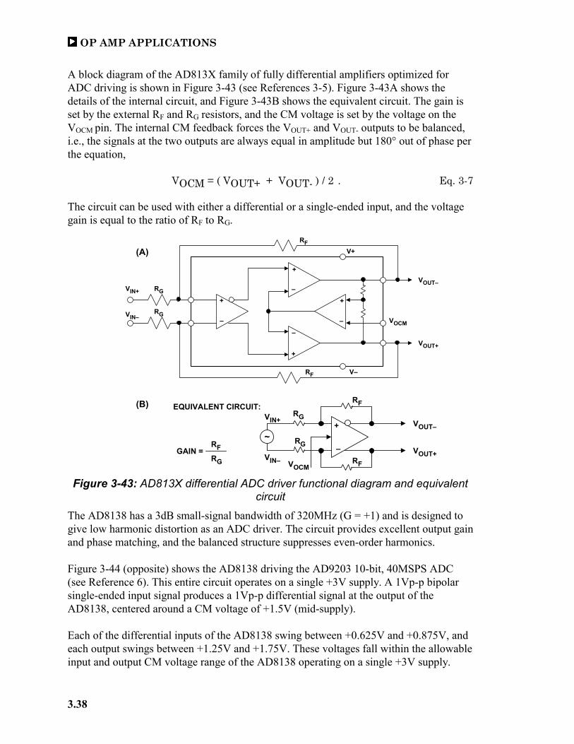
A block diagram of the AD813X family of fully differential amplifiers optimized for ADC driving is shown in Figure 3-43 (see References 3-5). Figure 3-43A shows the details of the internal circuit, and Figure 3-43B shows the equivalent circuit. The gain is set by the external RF and RG resistors, and the CM voltage is set by the voltage on the VOCM pin. The internal CM feedback forces the VOUT+ and VOUT- outputs to be balanced, i.e., the signals at the two outputs are always equal in amplitude but 180° out of phase per the equation,
VOCM = ( VOUT+ + VOUT- ) / 2 . Eq. 3-7
The circuit can be used with either a differential or a single-ended input, and the voltage gain is equal to the ratio of RF to RG.
Figure 3-43: AD813X differential ADC driver functional diagram and equivalent circuit
The AD8138 has a 3dB small-signal bandwidth of 320MHz (G = +1) and is designed to give low harmonic distortion as an ADC driver. The circuit provides excellent output gain and phase matching, and the balanced structure suppresses even-order harmonics. Figure 3-44 (opposite) shows the AD8138 driving the AD9203 10-bit, 40MSPS ADC (see Reference 6). This entire circuit operates on a single +3V supply. A 1Vp-p bipolar single-ended input signal produces a 1Vp-p differential signal at the output of the AD8138, centered around a CM voltage of +1.5V (mid-supply). Each of the differential inputs of the AD8138 swing between +0.625V and +0.875V, and each output swings between +1.25V and +1.75V. These voltages fall within the allowable input and output CM voltage range of the AD8138 operating on a single +3V supply.
~
RF
RF
RG
RG
VOUT–
VOUT+
+
–GAIN = RFRG
VIN+
VIN–
EQUIVALENT CIRCUIT:
VOCM
+
–
+
–
–
+
+
–
RF
RF
RG
RG
VIN+
VIN–
VOUT+
VOUT–
VOCM
V+
V–
(A)
(B)

USING OP AMPS WITH DATA CONVERTERS DRIVING ADC INPUTS
3.39
The circuit as shown operates on a 1Vp-p single-ended bipolar input signal, and the input span of the AD9203 ADC is set for 1Vp-p differential. If the signal input amplitude is increased to 2Vp-p, the span of the AD9203 must be set for 2Vp-p differential. Under these conditions, each of the AD8138 inputs must swing between +0.5V and +1V, and each of the outputs between +1V and +2V.
Figure 3-44: AD8138 driving AD9203 10-bit, 40MSPS ADC As shown in Figure 3-45 below, increasing the amplitude in this manner offers a slight improvement in low frequency SINAD due to the improvement in low frequency SNR.
Figure 3-45: SINAD and ENOB for AD9203 12-bit, 40MSPS ADC driven by AD8138 differential amplifier
But at the same time however, a degradation occurs in the high frequency SINAD because of the larger distortion due to the larger signal swings.
9.8
9.5
9.2
8.8
8.5
8.2
7.9
7.5
ENOB
INPUT FREQUENCY (MHz)
SINAD(dBc)
+
–
AD9203
AIN-
AIN+
VIN
±0.5V
49.9Ω
499Ω
499Ω
499Ω
523Ω
10kΩ
10kΩ
49.9Ω
49.9Ω
+1.5VVOCM
AD8138
0.1µF
0.1µF
20pF
0.1µF
20pF
+0.75V +/ - 0.125V
+1.5V - / + 0.25V
+1.5V +/ - 0.25V
Set for 1V p-pDifferentialInput Span
+3V

OP AMP APPLICATIONS
3.40
Overvoltage Considerations The input structures of most high performance ADCs are sensitive to overvoltage conditions because of the small geometry devices used in the designs. Although ADC inputs generally have ESD protection diodes connected from the analog input to each supply rail, these diodes are not designed to handle the large currents that can be generated from typical op amp drivers. Two good rules of thumb are to (1) limit the analog input voltage to no more than 0.3V above or below the positive and negative supply voltages, respectively, and (2) limit the analog input current to 5mA maximum in overvoltage conditions.
Figure 3-46: ADC input overvoltage protection circuits Several typical configurations for the drive amp/ADC interface are shown in Figure 3-46 above. In Figure 3-46A, the ADC requires no additional input protection because both the op amp and the ADC are driven directly from the same supply voltages. While the RS resistor is not required for overvoltage protection, it does serve to isolate the capacitive input of the ADC from the output of the op amp. Figure 3-46B shows a dual supply op amp driving a single supply ADC, with the +5V supply is shared between the two devices. The diode protects the input of the ADC in case the output of the op amp is driven below ground. A Schottky diode is used because of its low forward voltage drop and its low capacitance. The RS resistor is split into two equal resistors, and they are chosen to limit the ADC input fault current to 5mA maximum. Note that the RS resistor in conjunction with the ADC input capacitance forms a lowpass filter. If RS is made too large, the input bandwidth may be restricted. Figure 3-46C shows the condition where the op amp and the ADC are driven from separate supplies. Two Schottky diodes are required to protect the ADC under all power supply and signal conditions. As in 3-46A, the RS/2 resistors limit ADC fault current.
RS/2
+5V +5V
AMP
-5V
ADC
RS/2
(C) Separate Supplies
RS/2
+5V
AMP
-5V
ADC
RS/2
(B) Same +5V Supply
AMP ADC
+5V
RS
(A) Single or Dual, Same Supplies
(Or –5V)

USING OP AMPS WITH DATA CONVERTERS DRIVING ADC INPUTS
3.41
REFERENCES: DRIVING ADC INPUTS 1. Data sheet for AD8057/AD8058 Low Cost, High Performance Voltage Feedback, 325 MHz
Amplifiers, http://www.analog.com.
2. Chapter 8 of Walt Kester, Editor, Practical Design Techniques for Sensor Signal Conditioning, Analog Devices, 1999, ISBN: 0-916550-20-6.
3. Data sheet for AD8131 Low-Cost, High-Speed Differential Driver, http://www.analog.com
4. Data sheet for AD8132 Low-Cost, High-Speed Differential Amplifier, http://www.analog.com
5. Data sheet for AD8138 Low Distortion Differential ADC Driver, http://www.analog.com
6. Data Sheet for AD9203 10-Bit, 40 MSPS, 3V, 74mW A/D Converter, http://www.analog.com
7. Chapters 3-6, Walt Kester, Editor, Practical Analog Design Techniques, Analog Devices, 1995,
ISBN: 0-916550-16-8.
8. Chapters 4, 5, Walt Kester, Editor, High Speed Design Techniques, Analog Devices, 1996, ISBN: 0-916550-17-6.
9. Chapters 3, 4, Walt Kester, Editor, Mixed-Signal and DSP Design Techniques, Analog Devices,
2000, ISBN: 0-916550-23-0. 10. Chapters 4, 5, Walt Kester, Editor, Linear Design Seminar, Analog Devices, 1995, ISBN: 0-916550-
15-X.

OP AMP APPLICATIONS
3.42
NOTES:

USING OP AMPS WITH DATA CONVERTERS DRIVING ADC/DAC REFERENCE INPUTS
3.43
SECTION 4-4: DRIVING ADC/DAC REFERENCE INPUTS Walt Jung, Walt Kester It might seem odd to include a section on voltage references in a book devoted primarily to op amp applications, but the relevance will shortly become obvious. Unfortunately, there is little standardization with respect to ADC/DAC voltage references. Some ADCs and DACs have internal references, while others do not. In some cases, the DC accuracy of a converter with an internal reference can often be improved by overriding the internal reference with a more accurate and stable external one. Although the reference element itself can be either a bandgap, buried zener, or XFET™ (see Reference 1), practically all references have some type of output buffer op amp. The op amp isolates the reference element from the output and also provides drive capability. However, this op amp must obey the general laws relating to op amp stability, and that is what makes the topic of references relevant to the discussion. Figure 3-47 below summarizes voltage reference considerations.
Figure 3-47: ADC / DAC voltage reference considerations Note that a reference input to an ADC or DAC is similar to the analog input of an ADC, in that the internal conversion process can inject transient currents at that pin. This requires adequate decoupling to stabilize the reference voltage. Adding such decoupling might introduce instability in some reference types, depending on the output op amp design. Of course, a reference data sheet may not show any details of the output op amp, which leaves the designer in somewhat of a dilemma concerning whether or not it will be stable and free from transient errors. Fortunately, some simple lab tests can exercise a reference circuit for transient errors, and also determine stability for capacitive loading. Figure 3-48 shows the transients associated with the reference input of a typical successive approximation ADC. The ADC reference voltage input must be stabilized with a sufficiently large decoupling capacitor, in order to prevent conversion errors. The value of the capacitor required as CB may range from below 1µF, to as high as 100µF. This capacitor must of course have a voltage rating greater than the reference voltage. Physically, it will be of minimum size when purchased in a surface mount style.
Data converter accuracy determined by the reference, whether internal or external
Bandgap, buried zener, XFET™ generally have on-chip output buffer op amp
Transient loading can cause instability and errors
External decoupling capacitors may cause oscillation
Output may require external buffer to source and sink current
Reference voltage noise may limit system resolution

OP AMP APPLICATIONS
3.44
Note that in this case, a 1µF capacitor on the reference input is required to reduce the transients to an acceptable level. Note that the capacitor size can be electrically larger for further noise reduction— the tradeoff here is of course cost and PCB real estate. The AD780 will work with capacitors of up to 100µF.
Figure 3-48: Successive approximation ADCs can present a transient load to the reference
A well-designed voltage reference is stable with heavy capacitive decoupling. Unfortunately, some are not, as shown in Figure 3-49 below, where the addition of CL to the reference output (a 0.01µF capacitor) actually increases the amount of transient ringing. Such references are practically useless in data converter applications, because some amount of local decoupling is almost always required at the converter.
Figure 3-49: Make sure reference is stable with large capacitive loads A suitable op amp buffer might be added between the reference and the data converter. But, there are many good references available (such as the AD780) which are stable with an output capacitor. This type of reference should be chosen for a data converter application, rather than incurring the further complication and expense of an op amp.
AD780
VIN
CB
VREF
SCOPE
SCOPE
START CONVERT
STARTCONVERT
CB = 0.01µF
CB = 0.22µF
CB = 1µF
TOP TRACE VERTICAL SCALE: 5V/div.ALL OTHER VERTICAL SCALES: 5mV/div.HORIZONTAL SCALE: 1µs/div.
SARADC
REFERENCEUNDER
TEST
PULSEGENERATOR
VIN
CL RL
1mA to 2mA STEP SCOPE
TOP TRACE: NO LOAD (CL = 0) 50mV/div.
BOTTOM TRACE: CL = 0.01µF200mV/div.
BOTH TRACES: 5µs/div.

USING OP AMPS WITH DATA CONVERTERS DRIVING ADC/DAC REFERENCE INPUTS
3.45
If very low noise levels are required from a reference, an additional low pass filter followed by a low noise op amp can be used to achieve the desired performance. The reference circuit of Figure 3-50 is one such example (see References 2 and 3). This circuit uses external filtering and a precision low-noise op-amp to provide both very low noise and high DC accuracy. Reference U1 is a 2.5, 3.0, 5, or 10V reference with a low noise buffered output. The output of U1 is applied to the R1-C1/C2 noise filter to produce a corner frequency of about 1.7 Hz. Electrolytic capacitors usually imply DC leakage errors, but the bootstrap connection of C1 causes its applied bias voltage to be only the relatively small drop across R2. This lowers the leakage current through R1 to acceptable levels. Since the filter attenuation is modest below a few Hertz, the reference noise still affects overall performance at low frequencies (i.e., <10 Hz).
Figure 3-50: Low-noise op amp with filtering yields reference noise performance (1.5 to 5nV/√Hz @ 1kHz)
A precision low noise unity-gain follower, such as the OP113, then buffers the output of the filter. With less than ±150µV of offset error and under 1µV/°C drift, the buffer amplifier’s DC performance will not seriously affect the accuracy/drift of most references. For example, an ADR292E for U1 will have a typical drift of 3ppm/°C, equivalent to 7.5µV/°C, higher than the buffer amplifier. Almost any op amp will have a current limit higher than a typical IC reference, so this circuit allows greater current output. It also removes any load related thermal errors that might occur when the reference IC is loaded directly. Even lower noise op-amps are available, for 5-10V use. The AD797 offers 1kHz noise performance less than 2nV/√Hz in this circuit, compared to about 5nV/√Hz for the OP113. With any buffer amplifier, Kelvin sensing can be used at the load point, a technique that eliminates I×R related output voltage errors.
0.1µF
VIN VO
GND
R1
1kΩ
10kΩ
R2
C1
100µF25V
+
+ C2
100µF25V
100Ω
1.1kΩ
+100µF,25V
3.3Ω
+ 10µF25V
26
4
3
2
7
4
6100Ω
U1
U2
+
U1: AD586, AD587, REF01 REF02, REF05, REF10
U2: OP113, OP27 OP176, AD797
+15V +15V
DIODES:1N4148

OP AMP APPLICATIONS
3.46
REFERENCES: DRIVING ADC/DAC REFERENCE INPUTS 1. Chapter 2, Walt Kester, Editor, Practical Design Techniques for Power and Thermal Management,
Analog Devices, 1998, ISBN: 0-916550-19-2. 2. Walt Jung, "Build an Ultra-Low-Noise Voltage Reference," Electronic Design Analog Applications
Issue, June 24, 1993. 3. Walt Jung, "Getting the Most from IC Voltage References," Analog Dialogue, Vol. 28, No., 1994, pp.
13-21.

USING OP AMPS WITH DATA CONVERTERS BUFFERING DAC OUTPUTS
3.47
SECTION 3-5: BUFFERING DAC OUTPUTS Walt Kester, Paul Hendriks
General Considerations Another important op amp application is buffering DAC outputs. Modern IC DACs provide either voltage or current outputs. Figure 3-51 below shows three fundamental configurations, all with the objective of using an op amp for a buffered output voltage.
Figure 3-51: Buffering DAC outputs with op amps Figure 3-51A shows a buffered voltage output DAC. In many cases, the DAC output can be used directly, without additional buffering. If an additional op amp buffer is needed, it is usually configured in a non-inverting mode, with gain determined by R1 and R2. There are two basic methods for dealing with a current output DAC. In Figure 3-51B, a voltage is simply developed across external load resistor, RL. An external op amp can be used to buffer and/or amplify this voltage if required. Many DACs supply fullscale currents of 20mA or more, thereby allowing reasonable voltages to be developed across fairly low value load resistors. For instance, fast settling video DACs typically supply nearly 30mA fullscale current, allowing 1V to be developed across a source and load terminated 75Ω coaxial cable (representing a DC load of 37.5Ω to the DAC output). A direct method to convert the output current into a voltage is shown in Figure 3-51C, This circuit is usually called a current-to-voltage converter, or I/V. In this circuit, the DAC output drives the inverting input of an op amp, with the output voltage developed across the R2 feedback resistor. In this approach the DAC output always operates at virtual ground (which may give a linearity improvement vis-à-vis Fig. 3-51B). The general selection process for an op amp used as a DAC buffer is similar to that of an ADC buffer. The same basic specifications such as DC accuracy, noise, settling time, bandwidth, distortion, etc., apply to DACs as well as ADCs, and the discussion will not be repeated here. Rather, some specific application examples will be shown.
N
+
–VOUT
N
+
–IOUT
N +
–
IOUT
(A)
(B) (C)
RL R2R1
R2
R2R1
VOUT
1 + R2R1
IOUT•RL
–IOUT•R2
1 + R2R1+

OP AMP APPLICATIONS
3.48
Differential to Single-Ended Conversion Techniques A general model of a modern current output DAC is shown in Figure 3-52 below. This model is typical of the AD976X and AD977X TxDAC™ series (see Reference 1). Current output is more popular than voltage output, especially at audio frequencies and above. If the DAC is fabricated on a bipolar or BiCMOS process, it is likely that the output will sink current, and that the output impedance will be less than 500Ω (due to the internal R/2R resistive ladder network). On the other hand, a CMOS DAC is more likely to source output current and have a high output impedance, typically greater than 100kΩ.
Figure 3-52: Model of high speed DAC output Another consideration is the output compliance voltage— the maximum voltage swing allowed at the output in order for the DAC to maintain its linearity. This voltage is typically 1V to 1.5V, but can vary depending upon the DAC. Best DAC linearity is generally achieved when driving a virtual ground, such as an op amp I/V converter. Modern current output DACs usually have differential outputs, to achieve high CM rejection and reduce the even-order distortion products. Fullscale output currents in the range of 2mA to 20mA are common. In most applications, it is desirable to convert the differential output of the DAC into a single-ended signal, suitable for driving a coax line. This can be readily achieved with an RF transformer, provided low frequency response is not required. Figure 3-53 (opposite) shows a typical example of this approach. The high impedance current output of the DAC is terminated differentially with 50Ω, which defines the source impedance to the transformer as 50Ω.
ROUT
ROUT
IFS – I
I
IOUT
IOUT
RSET
IFS 2 - 20mA typicalBipolar or BiCMOS DACs sink current, ROUT < 500ΩCMOS DACs source current, ROUT > 100kΩOutput compliance voltage < ±1V for best performance
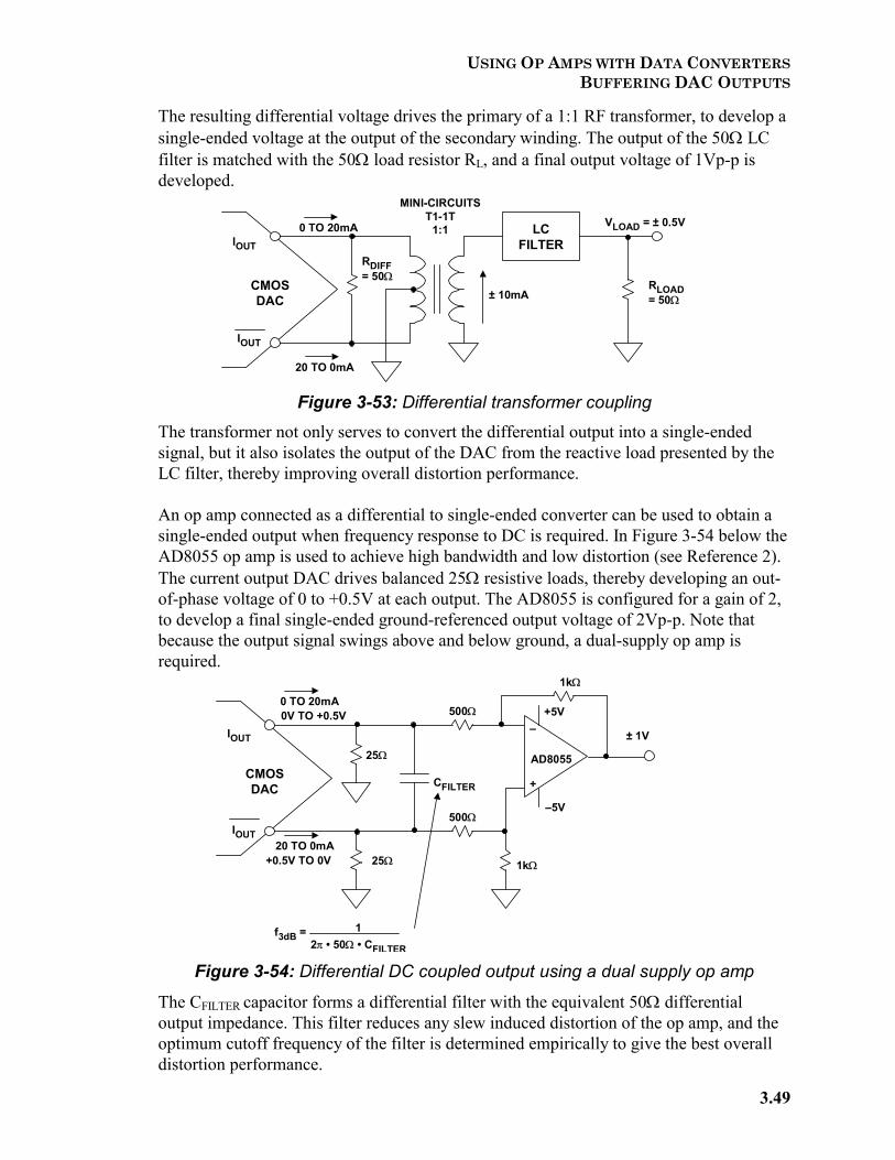
USING OP AMPS WITH DATA CONVERTERS BUFFERING DAC OUTPUTS
3.49
The resulting differential voltage drives the primary of a 1:1 RF transformer, to develop a single-ended voltage at the output of the secondary winding. The output of the 50Ω LC filter is matched with the 50Ω load resistor RL, and a final output voltage of 1Vp-p is developed.
Figure 3-53: Differential transformer coupling The transformer not only serves to convert the differential output into a single-ended signal, but it also isolates the output of the DAC from the reactive load presented by the LC filter, thereby improving overall distortion performance. An op amp connected as a differential to single-ended converter can be used to obtain a single-ended output when frequency response to DC is required. In Figure 3-54 below the AD8055 op amp is used to achieve high bandwidth and low distortion (see Reference 2). The current output DAC drives balanced 25Ω resistive loads, thereby developing an out-of-phase voltage of 0 to +0.5V at each output. The AD8055 is configured for a gain of 2, to develop a final single-ended ground-referenced output voltage of 2Vp-p. Note that because the output signal swings above and below ground, a dual-supply op amp is required.
Figure 3-54: Differential DC coupled output using a dual supply op amp
The CFILTER capacitor forms a differential filter with the equivalent 50Ω differential output impedance. This filter reduces any slew induced distortion of the op amp, and the optimum cutoff frequency of the filter is determined empirically to give the best overall distortion performance.
LCFILTER
MINI-CIRCUITST1-1T
1:1
RDIFF= 50Ω
RLOAD= 50Ω
VLOAD = ± 0.5VIOUT
IOUT
0 TO 20mA
20 TO 0mA
± 10mACMOSDAC
IOUT
IOUT
0 TO 20mA
20 TO 0mA
CMOSDAC
AD8055
+
–+5V
–5V
25Ω
25Ω
0V TO +0.5V
+0.5V TO 0V
CFILTER
500Ω
500Ω
1kΩ
1kΩ
± 1V
f3dB = 12π • 50Ω • CFILTER

OP AMP APPLICATIONS
3.50
A modified form of the Fig. 3-54 circuit can also be operated on a single supply, provided the CM voltage of the op amp is set to mid-supply (+2.5V). This is shown in Figure 3-55 below. The output voltage is 2Vp-p centered around a CM voltage of +2.5V. This CM voltage can be either developed from the +5V supply using a resistor divider, or directly from a +2.5V voltage reference. If the +5V supply is used as the CM voltage, it must be heavily decoupled to prevent supply noise from being amplified.
Figure 3-55: Differential DC coupled output using a single-supply op amp
Single-Ended Current-to-Voltage Conversion Single-ended current-to-voltage conversion is easily performed using a single op amp as an I/V converter, as shown in Figure 3-56 below. The 10mA fullscale DAC current from the AD768 (see Reference 3) develops a 0 to +2V output voltage across the 200Ω RF.
Figure 3-56: Single-ended I/V op amp interface for precision 16-bit AD768 DAC Driving the virtual ground of the AD8055 op amp minimizes any distortion due to nonlinearity in the DAC output impedance. In fact, most high resolution DACs of this type are factory trimmed using an I/V converter.
IOUT
IOUT
0 TO 10mA
AD76816-BIT
BiCMOSDAC
AD8055
+
–+5V
RF = 200Ω
–5V
RDAC||CDAC
CF
0 TO +2.0V
For RDAC ≈ RF, make CF ≈
CIN
RDAC (CDAC + CIN)RF
For RDAC >> RF, make CF ≈ CDAC + CIN2π RF fu
fu = Op Amp Unity Gain-Bandwidth Product
IOUT
IOUT
0 TO 20mA
20 TO 0mA
CMOSDAC
AD8055
+
–+5V
25Ω
25Ω
0V TO +0.5V
+0.5V TO 0V
CFILTER
500Ω
500Ω
2kΩ
1kΩ
± 1V
f3dB = 12π • 50Ω • CFILTER
+2.5V
+5V2kΩ
+2.5VREF
1kΩ
SEE TEXT
+5V

USING OP AMPS WITH DATA CONVERTERS BUFFERING DAC OUTPUTS
3.51
It should be recalled, however, that using the single-ended output of the DAC in this manner will cause degradation in the CM rejection and increased second-order distortion products, compared to a differential operating mode. The CF feedback capacitor should be optimized for best pulse response in the circuit. The equations given in the diagram should only be used as guidelines. A more detailed analysis of this circuit is given in Reference 6. Differential Current-to-Differential Voltage Conversion If a buffered differential voltage output is required from a current output DAC, the AD813X-series of differential amplifiers can be used as shown in Figure 3-57 below.
Figure 3-57: Buffering high speed DACs using AD813X differential amplifier
The DAC output current is first converted into a voltage that is developed across the 25Ω resistors. The voltage is amplified by a factor of 5 using the AD813X. This technique is used in lieu of a direct I/V conversion to prevent fast slewing DAC currents from overloading the amplifier and introducing distortion. Care must be taken so that the DAC output voltage is within its compliance rating. The VOCM input on the AD813X can be used to set a final output CM voltage within the range of the AD813X. If transmission lines are to be driven at the output, adding a pair of 75Ω resistors will allow this.
IOUT
IOUT
0 TO 20mA0 TO +0.5V
20 TO 0mA+0.5 TO 0V
CMOSDAC
+
–
AD813X
VOCM
2.49kΩ
2.49kΩ
5V p-pDIFFERENTIALOUTPUT
25Ω
25Ω
499Ω
499Ω

OP AMP APPLICATIONS
3.52
An Active Lowpass Filter for Audio DAC Figure 3-58 below shows an active lowpass filter which also serves as a current-to-voltage converter for the AD1853 sigma-delta audio DAC (see Reference 4). The filter is a 4-pole filter with a 3dB cutoff frequency of approximately 75kHz. Because of the high oversampling frequency (24.576MSPS when operating the DAC at a 48KSPS throughput rate), a simple filter is all that is required to remove aliased components above 12MHz).
Figure 3-58: A 75kHz 4-pole gaussian active filter for buffering the output of AD1853 stereo DAC
The diagram shows a single channel for the dual channel DAC output. U1A and U1B I/V stages form a 1-pole differential filter, while U2 forms a 2-pole multiple-feedback filter that also performs a differential-to-single-ended conversion. A final fourth passive pole is formed by the 604Ω resistor and the 2.2nF capacitor across the output. The OP275 op amp was chosen for operation at U1 and U2, and for its quality audio characteristics (see Reference 5). For further details of active filter designs, see Chapter 5 of this book.
4.12kΩ
4.12kΩ
330pF
330pF
2.74kΩ
2.74kΩ
2.74kΩ
2.74kΩ
2.94kΩ
2.94kΩ
220pF
220pF
604Ω
49.9kΩ2.2nF
+15V
–15V
+15V
–15V
402Ω
402Ω
–
+
+
–
–
+
ROUT+
ROUT–
VREF+2.75V
0mA TO +1.5mA
+1.5mA TO 0mA
RIGHTCHANNELOUTPUT
U1A1/2
OP275
U1B1/2
OP275
U2A1/2
OP275
NOTE: ONLY RIGHT CHANNEL SHOWNFROMAD1853DAC
680pF
680pF
220pF

USING OP AMPS WITH DATA CONVERTERS BUFFERING DAC OUTPUTS
3.53
REFERENCES: BUFFERING DAC OUTPUTS 1. Data sheet for AD9772A 14-Bit, 160 MSPS TxDAC+® with 2x Interpolation Filter,
http://www.analog.com 2. Data sheet for AD8055/AD8056 Low Cost, 300 MHz Voltage Feedback Amplifiers,
http://www.analog.com. 3. Data sheet for AD768 16-Bit, 30 MSPS D/A Converter, http://www.analog.com. 4. Data sheet for AD1853 Stereo, 24-Bit, 192 kHz, Multibit Σ∆ DAC, http://www.analog.com. 5. Data sheet for OP275 Dual Bipolar/JFET, Audio Operational Amplifier, http://www.analog.com. 6. Chapters 5, Walt Kester, Editor, Practical Design Techniques for Sensor Signal Conditioning,
Analog Devices, 1999, ISBN: 0-916550-20-6.

OP AMP APPLICATIONS
3.54
NOTES: