1 id 2 id -...
TRANSCRIPT

crystals
Review
Brief Review of Epitaxy and Emission Properties ofGaSb and Related Semiconductors
Shouzhu Niu 1 ID , Zhipeng Wei 1,*, Xuan Fang 1, Dengkui Wang 1, Xinwei Wang 1, Xian Gao 1
and Rui Chen 2 ID
1 State Key Laboratory of High Power Semiconductor Lasers, School of Science, Changchun University ofScience and Technology, 7089 Wei-Xing Road, Changchun 130022, China; [email protected] (S.N.);[email protected] (X.F.); [email protected] (D.W.); [email protected] (X.W.);[email protected] (X.G.)
2 Department of Electrical and Electronic Engineering, South University of Science and Technology of China,Shenzhen 518055, China; [email protected]
* Correspondence: [email protected]; Tel.: +86-158-4309-5977
Academic Editor: Paul J. SimmondsReceived: 31 August 2017; Accepted: 25 October 2017; Published: 2 November 2017
Abstract: Groups III–V semiconductors have received a great deal of attention because of theirpotential advantages for use in optoelectronic and electronic applications. Gallium antimonide(GaSb) and GaSb-related semiconductors, which exhibit high carrier mobility and a narrow band gap(0.725 eV at 300 K), have been recognized as suitable candidates for high-performance optoelectronicsin the mid-infrared range. However, the performances of the resulting devices are strongly dependenton the structural and emission properties of the materials. Enhancement of the crystal quality,adjustment of the alloy components, and improvement of the emission properties have thereforebecome the focus of research efforts toward GaSb semiconductors. Molecular beam epitaxy (MBE)is suitable for the large-scale production of GaSb, especially for high crystal quality and beneficialoptical properties. We review the recent progress in the epitaxy of GaSb materials, including films andnanostructures composed of GaSb-related alloys and compounds. The emission properties of thesematerials and their relationships to the alloy components and material structures are also discussed.Specific examples are included to provide insight on the common general physical and opticalproperties and parameters involved in the synergistic epitaxy processes. In addition, the furtherdirections for the epitaxy of GaSb materials are forecasted.
Keywords: gallium antimonide; alloys and compounds; nanostructures; photoluminescence;molecular beam epitaxy
1. Introduction
The mid-infrared (MIR) spectral region is of great research interest because the practical realizationof optoelectronic devices that operate in the 2–5 µm wavelength region would bring potentialapplications in a wide range of areas, including optical gas sensing, environmental monitoring,free-space optical communications, infrared countermeasures, and thermal imaging [1–3]. Researchinto MIR semiconductor devices has thus become a focus of research attention worldwide. GroupsIII–V semiconductors are the most promising candidate infrared materials for use in lasers anddetectors, owing to their high absorption coefficients, high carrier mobilities and widely tunableband gaps [1,4]. Among these materials, gallium antimonide (GaSb)-based alloys and compoundsoffer a wide range of electronic band gaps, band gap offsets and electronic barriers along withextremely high electron mobility; these materials would thus enable a variety of devices that aremuch faster than the equivalent InP- and GaAs-based devices and infrared light sources, and would
Crystals 2017, 7, 337; doi:10.3390/cryst7110337 www.mdpi.com/journal/crystals

Crystals 2017, 7, 337 2 of 21
facilitate lower power consumption [5,6]. Therefore, GaSb materials in the forms of epitaxial layers,multi-element alloys, quantum wells, superlattices and low-dimensional nanostructures have beenattracting considerable attention. Additionally, based on the GaSb materials described above, a varietyof advanced optoelectronic devices, including laser diodes, detectors, and transistors, have beenrealized [1–4].
Therefore, considerable effort has been devoted to the growth of high-quality GaSb-basedsemiconductor materials. To date, the growth of GaSb-based semiconductors has mainly beendependent on liquid phase epitaxy (LPE), metal-organic chemical vapor deposition (MOCVD),and molecular beam epitaxy (MBE). MBE is preferred as a high-efficiency epitaxial growth techniquethat is used to manufacture light-emitting diodes, lasers, and detectors for MIR waveband operationby varying the material components to adjust their energy bands [1,5,7]. By tuning of the growthparameters, a variety of complex quantum structures with high surface and interface quality can berealized. Problems that occur on the GaSb surface during reactive processing, such as high surfacestate densities, surface Fermi level pinning and a residual native oxide layer, have affected the opticalproperties, including their photoresponse range and luminescence intensities, of GaSb-based devices.Therefore, procedures that involve the removal of native oxides and the fabrication of passivationcoatings are necessary to overcome such problems [8]. Improvements in the surface properties of GaSbmaterials have led to excellent optoelectronic device performances. As the research into optoelectronicdevices has advanced, spectroscopic techniques have become increasingly important because theyare highly efficient and rapid modern analysis methods. These techniques can effectively determinethe photophysical properties of the materials and reveal their excited-state processes to determinetheir potential use in optoelectronic devices. Further development of spectroscopic techniques willtherefore be helpful in the design and improvement of the next generation of optoelectronic devices.Additionally, two-dimensional (2D) materials offer further promise for the development of a newrange of fundamental optoelectronic materials owing to their high crystal quality features and richphotophysical properties that will provide new material options for next generation optoelectronicdevices [2,8–10]. Therefore, owing to the advantages of 2D materials, further research should bedirected to the epitaxy and optical properties of GaSb materials.
In this paper, we briefly review the literature for the recent progress in the growth and the opticalproperties of GaSb and GaSb-related materials, and describe the evolution and the current status ofepitaxial growth processes and the optical properties of GaSb and related semiconductors. Section 2provides a brief introduction to some of the epitaxial GaSb materials that have already been grownby the MBE method, Section 3 covers the luminescence mechanism and the spectral characteristics ofthese materials, along with the factors that influence their optical properties. Section 4 is devoted to theeffects of low-dimensional nanostructures on the luminescence properties of these materials. Finally,we discuss GaSb materials fabricated by the MBE method that exhibit unusual optical properties andprovide a foundation for the application of these materials in optoelectronic devices.
2. Epitaxy of GaSb Materials
In this review, GaSb and related semiconductors refers to the groups III–V semiconductors thatcontain the Sb element, including GaAsSb, InAsSb, InGaAsSb and AlGaAsSb. Among these materials,GaSb has a prominent position among the III–V compound semiconductors. GaSb has a lattice constantof 6.0959 Å that mediates between ternary and quaternary III–V compound semiconducting materials(as shown in Figure 1), which enables perfect lattice matching of GaSb to be achieved with many III–Vphosphonium-type materials, which is then favorable for high-quality antimony material growth.Additionally, GaSb has a zinc blende (ZB) structure similar to that of GaAs, and its band gap is 0.822 eVat 0 K and 0.725 eV at 300 K [11–13].

Crystals 2017, 7, 337 3 of 21
Crystals 2017, 7, 337 3 of 21
Figure 1. Band gap as a function of lattice constant for III–V compounds and their ternary and quaternary alloys. Reproduced with permission from [11], copyright AIP Publishing LLC (2009).
Liquid phase epitaxy (LPE) was the earliest method used in the extended growth of GaSb-based materials, and there are numerous reports on the growth of GaSb by LPE techniques. In the early studies of the surface morphology and the electrical and optical properties of GaSb layers, it was observed that the growth temperature range of 500–550 °C for the Ga melt is the optimal range to produce high-quality layers with excellent surface morphologies [14]. While epilayers grown at low temperatures have low native defect concentrations, they have poor morphologies and thus are unsuitable for device applications [15]. The typical surface morphologies of GaSb epilayers that were grown at 550 °C from a 660 °C from an Sb-rich melt are as shown in Figure 2. CVD growth of GaSb has been reported by Jakowetzet et al. and MOCVD growth of GaSb has also been performed [16,17].
Figure 2. Typical surface morphologies of GaSb epilayers (a) grown on a (100) substrate at 550 °C from a Ga-rich melt and (b) on a 7° off-axis (111) substrate at 660 °C from an Sb-rich melt. Reproduced with permission from [15], copyright Springer (1995).
At present, antimony is mainly grown using molecular beam epitaxy (MBE) technology, which is based on a nonthermodynamic equilibrium. In recent years, following the development of the nonthermodynamic equilibrium, MBE has been widely used to fabricate a variety of both high-purity single crystals and ultra-fine structures and has thus greatly enhanced the evolution of research into antimony-based materials and devices. MBE is a technique in which single or complex components of an atomic beam or molecular beam are propelled to a heated substrate, are absorbed, migrate, and are deposited on that substrate under ultra-high vacuum conditions [18].
To improve the crystal quality of the epitaxy film, a buffer layer between the epitaxy film and substrate is commonly used, owing to the large difference in lattice constants. InAs, AlSb and GaSb can be used as buffer layers. Noh et al. reported that high quality GaSb films could be realized on a GaAs (001) substrate at low temperature, and the strain relief and structural properties of the GaSb films with different buffer layers were investigated [6]. Their results show that the insertion of an AlSb or GaSb buffer layer is very useful for improving the quality of the GaSb grown on GaAs substrates [6].
Figure 1. Band gap as a function of lattice constant for III–V compounds and their ternary andquaternary alloys. Reproduced with permission from [11], copyright AIP Publishing LLC (2009).
Liquid phase epitaxy (LPE) was the earliest method used in the extended growth of GaSb-basedmaterials, and there are numerous reports on the growth of GaSb by LPE techniques. In the earlystudies of the surface morphology and the electrical and optical properties of GaSb layers, it wasobserved that the growth temperature range of 500–550 ◦C for the Ga melt is the optimal rangeto produce high-quality layers with excellent surface morphologies [14]. While epilayers grown atlow temperatures have low native defect concentrations, they have poor morphologies and thus areunsuitable for device applications [15]. The typical surface morphologies of GaSb epilayers that weregrown at 550 ◦C from a 660 ◦C from an Sb-rich melt are as shown in Figure 2. CVD growth of GaSbhas been reported by Jakowetzet et al. and MOCVD growth of GaSb has also been performed [16,17].
Crystals 2017, 7, 337 3 of 21
Figure 1. Band gap as a function of lattice constant for III–V compounds and their ternary and quaternary alloys. Reproduced with permission from [11], copyright AIP Publishing LLC (2009).
Liquid phase epitaxy (LPE) was the earliest method used in the extended growth of GaSb-based materials, and there are numerous reports on the growth of GaSb by LPE techniques. In the early studies of the surface morphology and the electrical and optical properties of GaSb layers, it was observed that the growth temperature range of 500–550 °C for the Ga melt is the optimal range to produce high-quality layers with excellent surface morphologies [14]. While epilayers grown at low temperatures have low native defect concentrations, they have poor morphologies and thus are unsuitable for device applications [15]. The typical surface morphologies of GaSb epilayers that were grown at 550 °C from a 660 °C from an Sb-rich melt are as shown in Figure 2. CVD growth of GaSb has been reported by Jakowetzet et al. and MOCVD growth of GaSb has also been performed [16,17].
Figure 2. Typical surface morphologies of GaSb epilayers (a) grown on a (100) substrate at 550 °C from a Ga-rich melt and (b) on a 7° off-axis (111) substrate at 660 °C from an Sb-rich melt. Reproduced with permission from [15], copyright Springer (1995).
At present, antimony is mainly grown using molecular beam epitaxy (MBE) technology, which is based on a nonthermodynamic equilibrium. In recent years, following the development of the nonthermodynamic equilibrium, MBE has been widely used to fabricate a variety of both high-purity single crystals and ultra-fine structures and has thus greatly enhanced the evolution of research into antimony-based materials and devices. MBE is a technique in which single or complex components of an atomic beam or molecular beam are propelled to a heated substrate, are absorbed, migrate, and are deposited on that substrate under ultra-high vacuum conditions [18].
To improve the crystal quality of the epitaxy film, a buffer layer between the epitaxy film and substrate is commonly used, owing to the large difference in lattice constants. InAs, AlSb and GaSb can be used as buffer layers. Noh et al. reported that high quality GaSb films could be realized on a GaAs (001) substrate at low temperature, and the strain relief and structural properties of the GaSb films with different buffer layers were investigated [6]. Their results show that the insertion of an AlSb or GaSb buffer layer is very useful for improving the quality of the GaSb grown on GaAs substrates [6].
Figure 2. Typical surface morphologies of GaSb epilayers (a) grown on a (100) substrate at 550 ◦C froma Ga-rich melt and (b) on a 7◦ off-axis (111) substrate at 660 ◦C from an Sb-rich melt. Reproduced withpermission from [15], copyright Springer (1995).
At present, antimony is mainly grown using molecular beam epitaxy (MBE) technology, which isbased on a nonthermodynamic equilibrium. In recent years, following the development of thenonthermodynamic equilibrium, MBE has been widely used to fabricate a variety of both high-puritysingle crystals and ultra-fine structures and has thus greatly enhanced the evolution of research intoantimony-based materials and devices. MBE is a technique in which single or complex components ofan atomic beam or molecular beam are propelled to a heated substrate, are absorbed, migrate, and aredeposited on that substrate under ultra-high vacuum conditions [18].
To improve the crystal quality of the epitaxy film, a buffer layer between the epitaxy film andsubstrate is commonly used, owing to the large difference in lattice constants. InAs, AlSb and GaSbcan be used as buffer layers. Noh et al. reported that high quality GaSb films could be realized on aGaAs (001) substrate at low temperature, and the strain relief and structural properties of the GaSbfilms with different buffer layers were investigated [6]. Their results show that the insertion of an AlSbor GaSb buffer layer is very useful for improving the quality of the GaSb grown on GaAs substrates [6].

Crystals 2017, 7, 337 4 of 21
As an important part of GaSb materials, multi-component alloys have been intensivelyinvestigated. By tuning the components in the alloys, the band gap and lattice constant can beadjusted over a wide range. For example, by theoretical calculations, Wieder and Clawson determinedan expression for the band gap of InAsxSb1−x materials with composition x at temperature T,as follows [19]:
Eg(x, T) = 0.441− 3.4× 10⁻⁴T2
210 + T− 0.876x + 0.70x2 + 3.4× 10⁻⁴xT(1− x) (1)
Among the ternary alloys [20], GaAsxSb1−x is important owing to the advantage that itswavelength can be modulated over the range from 0.8 µm to 1.7 µm, and such a wavelength bandwould enable the production of optoelectronic devices with broad application prospects comparedwith those of InP- and GaAs-based devices. Chou et al. reported on the effects of substrate tiltingon the material properties of MBE grown GaAsSb alloys that were closely lattice-matched to InPsubstrates. GaAsSb alloys with a thickness of 1 µm were grown on InP(100) and off-axis InP substrates(2◦, 3◦ and 4◦ off-axis) and were characterized by XRD, as shown in Figure 3. Their results are expectedto be applicable to devices that incorporate MBE grown GaAsSb in their active layer [21]. However,using Sb as a surfactant would cause a difficulty in epitaxial growth, such as component distributionaggregation. Therefore, the regulation of alloy composition is very important. For this purpose,using a mixed beam, Wei’s group reported the carrier dynamics in GaAsSb ternary alloys grown byMBE. The growth conditions and Sb component of the GaAsSb alloy samples were as those shownin Table 1 [22]. The results indicated that the localized states are related to the Sb component of theGaAsSb alloy; however, this component also leads to poor crystal quality in the material, and theapplications of GaAsSb alloys are limited owing to the deterioration in quality.
Crystals 2017, 7, 337 4 of 21
As an important part of GaSb materials, multi-component alloys have been intensively investigated. By tuning the components in the alloys, the band gap and lattice constant can be adjusted over a wide range. For example, by theoretical calculations, Wieder and Clawson determined an expression for the band gap of InAsxSb1−x materials with composition x at temperature T, as follows [19]: Eg(x,T)=0.441-
3.4×10⁻⁴T2
210+T -0.876x+0.70x2+3.4×10⁻⁴xT(1-x) (1)
Among the ternary alloys [20], GaAsxSb1−x is important owing to the advantage that its wavelength can be modulated over the range from 0.8 µm to 1.7 µm, and such a wavelength band would enable the production of optoelectronic devices with broad application prospects compared with those of InP- and GaAs-based devices. Chou et al. reported on the effects of substrate tilting on the material properties of MBE grown GaAsSb alloys that were closely lattice-matched to InP substrates. GaAsSb alloys with a thickness of 1 µm were grown on InP(100) and off-axis InP substrates (2°, 3° and 4° off-axis) and were characterized by XRD, as shown in Figure 3. Their results are expected to be applicable to devices that incorporate MBE grown GaAsSb in their active layer [21]. However, using Sb as a surfactant would cause a difficulty in epitaxial growth, such as component distribution aggregation. Therefore, the regulation of alloy composition is very important. For this purpose, using a mixed beam, Wei’s group reported the carrier dynamics in GaAsSb ternary alloys grown by MBE. The growth conditions and Sb component of the GaAsSb alloy samples were as those shown in Table 1 [22]. The results indicated that the localized states are related to the Sb component of the GaAsSb alloy; however, this component also leads to poor crystal quality in the material, and the applications of GaAsSb alloys are limited owing to the deterioration in quality.
Figure 3. X-ray diffraction (XRD) of 1 µm-thick GaAsSb epi-grown layers on InP (100) and 2°, 3° and 4° off-axis InP (100) substrates. Reproduced with permission from [21], copyright AIP Publishing LLC (2013).
Table 1. Growth conditions of the GaAsSb alloy samples. Reproduced with permission from [22], copyright Nature Publishing Group (2016).
Sample Growth Temperature As/Sb Beam Ratio Sb Component 1 28:1 6% 2 600 °C 16:1 8% 3 7:1 9%
InGaAsSb, which is lattice-matched to GaSb, has been studied in particular depth, in part because it is an important active region constituent of diode lasers emitting in the 2–3 µm range [23]. Early work on the direct band gap in GaSb-rich GaInAsSb has been summarized by Karouta et al.,
Figure 3. X-ray diffraction (XRD) of 1 µm-thick GaAsSb epi-grown layers on InP (100) and 2◦, 3◦ and4◦ off-axis InP (100) substrates. Reproduced with permission from [21], copyright AIP PublishingLLC (2013).
Table 1. Growth conditions of the GaAsSb alloy samples. Reproduced with permission from [22],copyright Nature Publishing Group (2016).
Sample Growth Temperature As/Sb Beam Ratio Sb Component
1 28:1 6%2 600 ◦C 16:1 8%3 7:1 9%

Crystals 2017, 7, 337 5 of 21
InGaAsSb, which is lattice-matched to GaSb, has been studied in particular depth, in partbecause it is an important active region constituent of diode lasers emitting in the 2–3 µm range [23].Early work on the direct band gap in GaSb-rich GaInAsSb has been summarized by Karouta et al.,who proposed a bowing parameter of 0.6 eV [24]. In a recent report, an absorption layer compositionof In0.28Ga0.72As0.25Sb0.75 allowed for lattice matching to GaSb and demonstrated cut-off wavelengthsof 2.9 µm at 250 K and 3.0 µm at room temperature [25]. Figure 4 shows the photoluminescence resultsrecorded between 4 and 300 K. Additionally, short-wave infrared barriode detectors can be realized.
Crystals 2017, 7, 337 5 of 21
who proposed a bowing parameter of 0.6 eV [24]. In a recent report, an absorption layer composition of In0.28Ga0.72As0.25Sb0.75 allowed for lattice matching to GaSb and demonstrated cut-off wavelengths of 2.9 µm at 250 K and 3.0 µm at room temperature [25]. Figure 4 shows the photoluminescence results recorded between 4 and 300 K. Additionally, short-wave infrared barriode detectors can be realized.
Figure 4. (a) Photoluminescence results measured between 4 and 300 K and (b) normalized spectral response data between 190 and 300 K. Reproduced with permission from [25], copyright AIP Publishing LLC (2015)
In a similar way to InGaAsSb, AlGaAsSb is also important, as it is lattice-matched to GaSb and forms a natural barrier and cladding material for use in mid-infrared semiconductor lasers. The relationships for the direct and indirect energy gaps were calculated by Adachi and the experimental results were summarized by Ait-Kaci et al. [26,27]. An accurate determination of the chemical composition of AlGaAsSb layers is difficult. Figure 5 shows the band-gap energies as a function of the x-composition parameter for AlxGa1−xAsySb1−y when it is lattice-matched to GaSb.
Figure 5. Band-gap energies as a function of the x-composition parameter for AlxGa1−xAsySb1−y when lattice matched to GaSb. Reproduced with permission from [26], copyright AIP Publishing LLC (1987)
In a recent study, Jasik et al. reported on their investigation of the composition of MBE-grown AlGaAsSb layers in the context of unintentional arsenic incorporation. Based on the results obtained, a procedure for the determination of the chemical composition of AlGaAsSb materials was proposed. Table 2 lists the chemical compositions of multicomponent layers [28].
Figure 4. (a) Photoluminescence results measured between 4 and 300 K and (b) normalized spectralresponse data between 190 and 300 K. Reproduced with permission from [25], copyright AIP PublishingLLC (2015).
In a similar way to InGaAsSb, AlGaAsSb is also important, as it is lattice-matched to GaSband forms a natural barrier and cladding material for use in mid-infrared semiconductor lasers.The relationships for the direct and indirect energy gaps were calculated by Adachi and theexperimental results were summarized by Ait-Kaci et al. [26,27]. An accurate determination of thechemical composition of AlGaAsSb layers is difficult. Figure 5 shows the band-gap energies as afunction of the x-composition parameter for AlxGa1−xAsySb1−y when it is lattice-matched to GaSb.
Crystals 2017, 7, 337 5 of 21
who proposed a bowing parameter of 0.6 eV [24]. In a recent report, an absorption layer composition of In0.28Ga0.72As0.25Sb0.75 allowed for lattice matching to GaSb and demonstrated cut-off wavelengths of 2.9 µm at 250 K and 3.0 µm at room temperature [25]. Figure 4 shows the photoluminescence results recorded between 4 and 300 K. Additionally, short-wave infrared barriode detectors can be realized.
Figure 4. (a) Photoluminescence results measured between 4 and 300 K and (b) normalized spectral response data between 190 and 300 K. Reproduced with permission from [25], copyright AIP Publishing LLC (2015)
In a similar way to InGaAsSb, AlGaAsSb is also important, as it is lattice-matched to GaSb and forms a natural barrier and cladding material for use in mid-infrared semiconductor lasers. The relationships for the direct and indirect energy gaps were calculated by Adachi and the experimental results were summarized by Ait-Kaci et al. [26,27]. An accurate determination of the chemical composition of AlGaAsSb layers is difficult. Figure 5 shows the band-gap energies as a function of the x-composition parameter for AlxGa1−xAsySb1−y when it is lattice-matched to GaSb.
Figure 5. Band-gap energies as a function of the x-composition parameter for AlxGa1−xAsySb1−y when lattice matched to GaSb. Reproduced with permission from [26], copyright AIP Publishing LLC (1987)
In a recent study, Jasik et al. reported on their investigation of the composition of MBE-grown AlGaAsSb layers in the context of unintentional arsenic incorporation. Based on the results obtained, a procedure for the determination of the chemical composition of AlGaAsSb materials was proposed. Table 2 lists the chemical compositions of multicomponent layers [28].
Figure 5. Band-gap energies as a function of the x-composition parameter for AlxGa1−xAsySb1−y whenlattice matched to GaSb. Reproduced with permission from [26], copyright AIP Publishing LLC (1987).
In a recent study, Jasik et al. reported on their investigation of the composition of MBE-grownAlGaAsSb layers in the context of unintentional arsenic incorporation. Based on the results obtained,a procedure for the determination of the chemical composition of AlGaAsSb materials was proposed.Table 2 lists the chemical compositions of multicomponent layers [28].

Crystals 2017, 7, 337 6 of 21
Table 2. Chemical compositions of multicomponent layers. (Reproduced with permission from Jasiket al., Journal of Applied Physics; published by the American Institute of Physics, 2011 [28]).
Sample RelaxationDegree (%)
Stoichiometry Coefficientx y
LatticeConstant
(Å)
LatticeMismatch (ppm),
Relaxed
LatticeMismatch
(ppm),(sinθs/sinθL)−1
#A01T 45 0.430 – 6.11255 2814 2837#A02T 10 0.355 – 6.10956 2324 4267#A03T 44 0.480 – 6.11455 3142 4782#A01Q 0 0.430 0.0437 6.09277 −431 −820#A02Q 10 0.355 0.0045 6.10753 1989 3664#A03Q 0 0.480 0.0319 6.09997 750 1463
3. Optical and Emission Properties of GaSb Materials
Optical properties have also been intensely investigated as a standard for evaluating materialquality and device performance. At present, GaSb materials are believed to have potential foroptoelectronic applications. To exploit the full potential of these materials for structural design,a clear understanding of the properties of the material system, e.g., the band parameters and carrierdynamics, is required. Photoluminescence (PL) is a type of spontaneous emission in which light isemitted from a material. The peak energy and intensity of PL are mostly dependent on the regions inthe materials that are excited. Basically, PL measurement is a useful tool for the characterization ofmaterial parameters and is helpful for understanding the dynamic carrier processes in materials [29].For example, PL measurements are advantageous in studies of optical emission processes, materialcomposition, and impurity content. To give an overview of the optical properties of GaSb materials,we will first review the previous work in this field over recent decades.
3.1. GaSb Emission Properties
Undoped GaSb is a direct band gap semiconductor with a gap of approximately 0.8 eV, which isalways p-type. In 1997, Dutta et al. presented a comprehensive review of GaSb growth technology,including the resulting structural, electronic and transport properties, along with a few opticalproperties [11]. In this section, we will provide a brief review of the PL properties of GaSb materials.
The luminescence properties of undoped p-GaSb were studied as early as 1972 by Jakowetzet al., who observed that a doubly-ionizable acceptor affected the concentration of holes in undopedGaSb [16]. Figure 6 shows the experimental PL data for undoped GaSb. The peak emission at 810 meVwas attributed to a free exciton, and the emission line at 795.5 meV was identified as arising fromto a bound exciton [30]. The lines A, B and C were interpreted as transitions from the conductionband to the three acceptor levels. The acceptor ionization energies denoted by EA, EB and EC were34.5, 55 and 102 meV, respectively [16,31–33]. The energy positions and corresponding interpretationsare listed in Table 3. Jakowetz et al. concluded that the simplest possible model for the acceptoris that of an antistructure defect, that is, as a Ga atom on an Sb site. However, they also admittedthat it may possible for more complex defect structures in undoped GaSb to exist. According tothe work of Lee et al., unintentionally doped GaSb can display approximately 20 transitions inthe 680–810 meV range in the low temperature PL spectra. While a few of these transitions haveclear associations with specific defects, the PL measurements offer great advantages for furtherresearch. The PL properties can be very different when using a specific growth method or specificgrowth conditions. For samples grown using MBE technology, better crystallinity is obtained whenusing a growth temperature range of 500–550 ◦C and an Sb4:Ga flux ratio of more than 1.5 [34].In another study, buffer layers were used to reduce the defect concentrations [35]. Clearly, high-qualityMBE-grown GaSb, which demonstrates higher carrier mobility, can be obtained by the optimizationof the growth conditions [33–36]. More importantly, PL measurements can serve to determine thetransitions that occur in good quality GaSb materials [33]. First, the free exciton (FE) transition is anindication of high optical quality. However, several bound excitonic transitions (BE1–BE4) are generally

Crystals 2017, 7, 337 7 of 21
observed and tend to dominate the emissions from MBE-grown samples. These acceptor-relatedtransitions are listed in Table 4. Additionally, the transition energy may be caused by a concentrationof unintentionally incorporated donors, strain effects, or competing free-to-bound and donor-acceptortransitions. More recently, researchers found that the free electron to hole bound to unidentifiedacceptor transition could dominate recombination after Te doping of GaSb, particularly at high dopinglevels [36]. Since then, the PL properties caused by doping effects have attracted scientific andtechnological interest motivated by optoelectronic device design considerations [37]. As the growthtechniques matured, the next challenge was to fabricate ternary and quaternary alloys to meet therequirements of heterostructure fabrication.
Crystals 2017, 7, 337 7 of 21
acceptor-related transitions are listed in Table 4. Additionally, the transition energy may be caused by a concentration of unintentionally incorporated donors, strain effects, or competing free-to-bound and donor-acceptor transitions. More recently, researchers found that the free electron to hole bound to unidentified acceptor transition could dominate recombination after Te doping of GaSb, particularly at high doping levels [36]. Since then, the PL properties caused by doping effects have attracted scientific and technological interest motivated by optoelectronic device design considerations [37]. As the growth techniques matured, the next challenge was to fabricate ternary and quaternary alloys to meet the requirements of heterostructure fabrication.
Figure 6. Experimental photoluminescence (PL) data for undoped GaSb. (a) PL spectrum of GaSb sample W4, grown from a stoichiometric melt. p300 = 1.8 × 1017 cm−8, T = 2 K; (b) PL spectrum of GaSb sample W7, grown from an antimony rich melt. p300 = 3.5 × 1016 cm−3, T = 2 K; Reproduced with permission from [16], copyright Wiley-VCH (1972).
Table 3. Energetic positions and corresponding interpretations for GaSb. Reproduced with permission from Jakowetz et al., Physica Status Solidi; published by the Weinheim, Germany: Wiley-VCH, 1972 [16].
line hυ (mev) FE 810 free exciton BE 795.5 bound exciton
A 777.5 band-acceptor transition
EA = 34.5 meV
BE-LO 766 phonon replica of line BE
(LO)Γ-phonon: (hυ)Ph = 29.5 meV
B 757 band-acceptor transition
EB = 55 meV
A-LO 748.5 phonon replica of line A
(LO)Γ-phonon: (hυ)Ph = 29 meV
B-LO 728 phonon replica of line B
(LO)Γ-phonon: (hυ)Ph = 29 meV
Figure 6. Experimental photoluminescence (PL) data for undoped GaSb. (a) PL spectrum of GaSbsample W4, grown from a stoichiometric melt. p300 = 1.8 × 1017 cm−8, T = 2 K; (b) PL spectrum ofGaSb sample W7, grown from an antimony rich melt. p300 = 3.5 × 1016 cm−3, T = 2 K; Reproducedwith permission from [16], copyright Wiley-VCH (1972).
Table 3. Energetic positions and corresponding interpretations for GaSb. Reproduced with permissionfrom Jakowetz et al., Physica Status Solidi; published by the Weinheim, Germany: Wiley-VCH,1972 [16].
Line hυ (mev)
FE 810 free exciton
BE 795.5 bound exciton
A 777.5 band-acceptor transitionEA = 34.5 meV
BE-LO 766 phonon replica of line BE(LO)Γ-phonon: (hυ)Ph = 29.5 meV
B 757 band-acceptor transitionEB = 55 meV
A-LO 748.5 phonon replica of line A(LO)Γ-phonon: (hυ)Ph = 29 meV
B-LO 728 phonon replica of line B(LO)Γ-phonon: (hυ)Ph = 29 meV
C 710band-acceptor transition
Ec = 102 meVsecond ionization step of the acceptor involved in line A
D 803 band-acceptor transition?ED = 9 meV
Crystals 2017, 7, 337 8 of 21
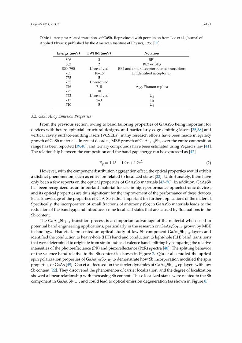
Table 4. Acceptor-related transitions of GaSb. Reproduced with permission from Lee et al., Journal ofApplied Physics; published by the American Institute of Physics, 1986 [33].
Energy (meV) FWHM (meV) Notation
806 3 BE1802 2 BE2 or BE3
800–790 Unresolved BE4 and other acceptor related transitions785 10–15 Unidentified acceptor U1775 5757 Unresolved746 7–8 ALO Phonon replica725 10722 Unresolved U2717 2–3 U3710 5 U4
3.2. GaSb Alloy Emission Properties
From the previous section, owing to band tailoring properties of GaAsSb being important fordevices with hetero-epitaxial structural designs, and particularly edge-emitting lasers [35,38] andvertical cavity surface-emitting lasers (VCSELs), many research efforts have been made in epitaxygrowth of GaSb materials. In recent decades, MBE growth of GaAs1−xSbx over the entire compositionrange has been reported [39,40], and ternary compounds have been estimated using Vegard’s law [41].The relationship between the composition and the band gap energy can be expressed as [42]
Eg = 1.43− 1.9x + 1.2x2 (2)
However, with the component distribution aggregation effect, the optical properties would exhibita distinct phenomenon, such as emission related to localized states [22]. Unfortunately, there haveonly been a few reports on the optical properties of GaAsSb materials [43–50]. In addition, GaAsSbhas been recognized as an important material for use in high-performance optoelectronic devices,and its optical properties are thus significant for the improvement of the performance of these devices.Basic knowledge of the properties of GaAsSb is thus important for further applications of the material.Specifically, the incorporation of small fractions of antimony (Sb) in GaAsSb materials leads to thereduction of the band gap and introduces some localized states that are caused by fluctuations in theSb content.
The GaAsxSb1−x transition process is an important advantage of the material when used inpotential band engineering applications, particularly in the research on GaAsxSb1−x grown by MBEtechnology. Hsu et al. presented an optical study of low-Sb-component GaAsxSb1−x layers andidentified the conduction to heavy-hole (HH) band and conduction to light-hole (LH) band transitionsthat were determined to originate from strain-induced valence band splitting by comparing the relativeintensities of the photoreflectance (PR) and piezoreflectance (PzR) spectra [48]. The splitting behaviorof the valence band relative to the Sb content is shown in Figure 7. Qiu et al. studied the opticalspin polarization properties of GaAs0.94Sb0.06 to demonstrate how Sb incorporation modified the spinproperties of GaAs [49]. Gao et al. focused on the carrier dynamics of GaAsxSb1−x epilayers with lowSb content [22]. They discovered the phenomenon of carrier localization, and the degree of localizationshowed a linear relationship with increasing Sb content. These localized states were related to the Sbcomponent in GaAsxSb1−x, and could lead to optical emission degeneration (as shown in Figure 8.).

Crystals 2017, 7, 337 9 of 21Crystals 2017, 7, 337 9 of 21
Figure 7. Valence band splitting behavior with respect to the Sb content of GaAsxSb1−x. PR spectra (dotted curves) of GaAs1−x Sbx samples for (a) Sb = 5.9%, (c)Sb = 8.4% and (e) Sb = 9.7% at 15, 77, 150, and 300 K. The full lines are least-squares fits to FDLL; Temperature variations of the experimental PR values for HH and LH transition with representative error bars for GaAs1−xSbx with (b) Sb = 5.9%, (d) Sb = 8.4%, and (f) Sb = 9.7% as open-circles and open-diamonds, respectively. The obtained values of the transition energies are indicated by the arrows. Reproduced with permission from [48], copyright Elsevier S. A. (2010).
Figure 8. (a) PL spectra of GaAsxSb1−x alloy samples at 10 K; the inset shows the PL spectrum of GaAs substrate at 10 K, (b) temperature-dependent PL characteristics of GaAsSb, and (c) (i) temperature dependent peak position and (ii) temperature dependent FWHM of the samples. Reproduced with permission from [22], copyright Nature Publishing Group (2016).
Figure 7. Valence band splitting behavior with respect to the Sb content of GaAsxSb1−x. PR spectra(dotted curves) of GaAs1−xSbx samples for (a) Sb = 5.9%, (c) Sb = 8.4% and (e) Sb = 9.7% at 15, 77, 150,and 300 K. The full lines are least-squares fits to FDLL; Temperature variations of the experimental PRvalues for HH and LH transition with representative error bars for GaAs1−xSbx with (b) Sb = 5.9%,(d) Sb = 8.4%, and (f) Sb = 9.7% as open-circles and open-diamonds, respectively. The obtained valuesof the transition energies are indicated by the arrows. Reproduced with permission from [48], copyrightElsevier S. A. (2010).
Crystals 2017, 7, 337 9 of 21
Figure 7. Valence band splitting behavior with respect to the Sb content of GaAsxSb1−x. PR spectra (dotted curves) of GaAs1−x Sbx samples for (a) Sb = 5.9%, (c)Sb = 8.4% and (e) Sb = 9.7% at 15, 77, 150, and 300 K. The full lines are least-squares fits to FDLL; Temperature variations of the experimental PR values for HH and LH transition with representative error bars for GaAs1−xSbx with (b) Sb = 5.9%, (d) Sb = 8.4%, and (f) Sb = 9.7% as open-circles and open-diamonds, respectively. The obtained values of the transition energies are indicated by the arrows. Reproduced with permission from [48], copyright Elsevier S. A. (2010).
Figure 8. (a) PL spectra of GaAsxSb1−x alloy samples at 10 K; the inset shows the PL spectrum of GaAs substrate at 10 K, (b) temperature-dependent PL characteristics of GaAsSb, and (c) (i) temperature dependent peak position and (ii) temperature dependent FWHM of the samples. Reproduced with permission from [22], copyright Nature Publishing Group (2016).
Figure 8. (a) PL spectra of GaAsxSb1−x alloy samples at 10 K; the inset shows the PL spectrum of GaAssubstrate at 10 K, (b) temperature-dependent PL characteristics of GaAsSb, and (c) (i) temperaturedependent peak position and (ii) temperature dependent FWHM of the samples. Reproduced withpermission from [22], copyright Nature Publishing Group (2016).

Crystals 2017, 7, 337 10 of 21
The localized states may be generated by the composition fluctuation, which should thereforebe suppressed to optimize the optical properties of the material. However, post annealing treatmenthas been commonly used to improve the structural and optical properties quality of semiconductors,and can be used to reduce the localized states occurring in GaAsxSb1−x layers. It should be notedthat the formation of localized states was related to Sb cluster formation inside the GaAsxSb1−xalloy, which was influenced by the rapid thermal annealing (RTA) temperature. Figure 9 shows theeffects of the RTA temperature on the emission properties [50]. During the RTA process, a significantchange in the PL, owing to the reduction of localized states, was observed. The distribution of thecomposition in GaAsxSb1−x resulting from the annealing can cause a slight red-shift of the maximumphotoluminescence peak. More important, the RTA process can induce Sb migration and a fluctuationin alloy composition; therefore, the optimal RTA temperature should be used to improve the opticalproperties of the GaAsxSb1−x alloy material.
Crystals 2017, 7, 337 10 of 21
The localized states may be generated by the composition fluctuation, which should therefore be suppressed to optimize the optical properties of the material. However, post annealing treatment has been commonly used to improve the structural and optical properties quality of semiconductors, and can be used to reduce the localized states occurring in GaAsxSb1−x layers. It should be noted that the formation of localized states was related to Sb cluster formation inside the GaAsxSb1−x alloy, which was influenced by the rapid thermal annealing (RTA) temperature. Figure 9 shows the effects of the RTA temperature on the emission properties [50]. During the RTA process, a significant change in the PL, owing to the reduction of localized states, was observed. The distribution of the composition in GaAsxSb1−x resulting from the annealing can cause a slight red-shift of the maximum photoluminescence peak. More important, the RTA process can induce Sb migration and a fluctuation in alloy composition; therefore, the optimal RTA temperature should be used to improve the optical properties of the GaAsxSb1−x alloy material.
Figure 9. Effects of rapid thermal annealing (RTA) temperature on the emission properties of GaAsxSb1−x. Reproduced with permission from Gao et al., Optical Materials Express; published by the Optical Society of America, 2017 [50].
3.3. Effects of Surface States on GaSb Materials
The superficial and interfacial characteristics can affect the performance of semiconductor devices. The surfaces of GaSb materials can oxidize rapidly in the atmosphere because of their highly reactive chemical properties, and the performance of devices based on these materials is largely dependent on the properties of the surfaces or interfaces. The development of GaSb-based devices could thus easily be hampered by the surface properties of the material. Generally, these surface states can lead to the poor photoelectric efficiency of optoelectronic devices. Specifically, an oxide layer forms during the oxidation process and an undesirable conduction path arises at the oxide/GaSb-based material interface because of the elemental Sb content [51]. Surface states are induced by these native oxides and can cause high surface recombination velocities and large leakage currents [52–55]. With the intent to improve these surface properties, various chemical treatments have been used to reduce the surface states in GaSb materials and thus improve the properties of the materials. In particular, the sulfuration technique (a surface treatment using a sulfur-containing solution) is showing potential to improve the density of surface states for surface passivation of III–V compounds. A number of works have focused on the use of models to describe the sulfur passivation process. One of the most widely accepted models can be expressed using the following form [54]: + + → ( ) , + ( ) , , + + ↑ (3)
The sulfur passivation process can be described using the schematic diagram shown in Figure 10. The first stage involves breaking the bonds between the AIII and BV−atoms (as shown in Figure 10a).
Figure 9. Effects of rapid thermal annealing (RTA) temperature on the emission properties ofGaAsxSb1−x. Reproduced with permission from Gao et al., Optical Materials Express; publishedby the Optical Society of America, 2017 [50].
3.3. Effects of Surface States on GaSb Materials
The superficial and interfacial characteristics can affect the performance of semiconductor devices.The surfaces of GaSb materials can oxidize rapidly in the atmosphere because of their highly reactivechemical properties, and the performance of devices based on these materials is largely dependenton the properties of the surfaces or interfaces. The development of GaSb-based devices could thuseasily be hampered by the surface properties of the material. Generally, these surface states can lead tothe poor photoelectric efficiency of optoelectronic devices. Specifically, an oxide layer forms duringthe oxidation process and an undesirable conduction path arises at the oxide/GaSb-based materialinterface because of the elemental Sb content [51]. Surface states are induced by these native oxidesand can cause high surface recombination velocities and large leakage currents [52–55]. With the intentto improve these surface properties, various chemical treatments have been used to reduce the surfacestates in GaSb materials and thus improve the properties of the materials. In particular, the sulfurationtechnique (a surface treatment using a sulfur-containing solution) is showing potential to improve thedensity of surface states for surface passivation of III–V compounds. A number of works have focusedon the use of models to describe the sulfur passivation process. One of the most widely acceptedmodels can be expressed using the following form [54]:
AI I I BV + HS− + H2O→(
AI I I)
X, Sy +
(BV
)X
, Sy + OH− + H2 ↑ (3)

Crystals 2017, 7, 337 11 of 21
The sulfur passivation process can be described using the schematic diagram shown in Figure 10.The first stage involves breaking the bonds between the AIII and BV− atoms (as shown in Figure 10a).Next, the chemical bonds are released to enable the formation of S-AIII and/or S-BV (as shownin Figure 10b). Then, chemical bonds are formed between sulfur and the other atoms on thesemiconductor surface (as shown in Figure 10c,d). We therefore present some examples to introducethe wet method used for the sulfur passivation process.
Crystals 2017, 7, 337 11 of 21
Next, the chemical bonds are released to enable the formation of S-AIII and/or S-BV (as shown in Figure 10b). Then, chemical bonds are formed between sulfur and the other atoms on the semiconductor surface (as shown in Figure 10c,d). We therefore present some examples to introduce the wet method used for the sulfur passivation process.
Figure 10. Schematic showing the chemical bonds between sulfur and other atoms formed at the semiconductor surface. Reproduced with permission from [8], copyright NORTH-HOLLAND (2013).
Wet methods of sulfur passivation based on the use of sulfur solutions have been proved to effectively reduce the surface states. For example, (NH4)2S and Na2S solutions are usually used to passivate GaSb surfaces [8]. Figure 11 presents the passivation time-dependent emission intensities of GaSb samples. The PL results indicate that the emission intensity of the passivated GaSb sample could be raised to be 15 times higher than that of the as-grown samples. From low temperature PL measurements, the reason for the enhanced emission intensity was determined to originate from the enhancement of free exciton emission. This wet method of sulfur passivation of GaSb-based materials is thus demonstrated to be promising for the development of efficient light-emitting materials, which means the application of GaSb materials in potential optoelectronic device is feasible [55].
Figure 10. Schematic showing the chemical bonds between sulfur and other atoms formed at thesemiconductor surface. Reproduced with permission from [8], copyright NORTH-HOLLAND (2013).
Wet methods of sulfur passivation based on the use of sulfur solutions have been proved toeffectively reduce the surface states. For example, (NH4)2S and Na2S solutions are usually used topassivate GaSb surfaces [8]. Figure 11 presents the passivation time-dependent emission intensitiesof GaSb samples. The PL results indicate that the emission intensity of the passivated GaSb samplecould be raised to be 15 times higher than that of the as-grown samples. From low temperature PLmeasurements, the reason for the enhanced emission intensity was determined to originate fromthe enhancement of free exciton emission. This wet method of sulfur passivation of GaSb-basedmaterials is thus demonstrated to be promising for the development of efficient light-emitting materials,which means the application of GaSb materials in potential optoelectronic device is feasible [55].
Crystals 2017, 7, 337 12 of 21
Crystals 2017, 7, 337 12 of 21
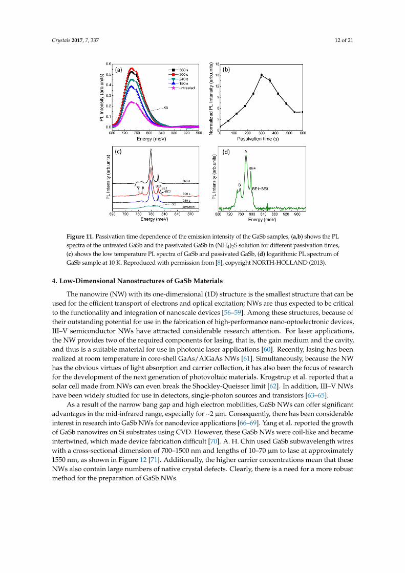
Figure 11. Passivation time dependence of the emission intensity of the GaSb samples, (a,b) shows the PL spectra of the untreated GaSb and the passivated GaSb in (NH4)2S solution for different passivation times, (c) shows the low temperature PL spectra of GaSb and passivated GaSb, (d) logarithmic PL spectrum of GaSb sample at 10 K. Reproduced with permission from [8], copyright NORTH-HOLLAND (2013).
4. Low-Dimensional Nanostructures of GaSb Materials
The nanowire (NW) with its one-dimensional (1D) structure is the smallest structure that can be used for the efficient transport of electrons and optical excitation; NWs are thus expected to be critical to the functionality and integration of nanoscale devices [56–59]. Among these structures, because of their outstanding potential for use in the fabrication of high-performance nano-optoelectronic devices, III–V semiconductor NWs have attracted considerable research attention. For laser applications, the NW provides two of the required components for lasing, that is, the gain medium and the cavity, and thus is a suitable material for use in photonic laser applications [60]. Recently, lasing has been realized at room temperature in core-shell GaAs/AlGaAs NWs [61]. Simultaneously, because the NW has the obvious virtues of light absorption and carrier collection, it has also been the focus of research for the development of the next generation of photovoltaic materials. Krogstrup et al. reported that a solar cell made from NWs can even break the Shockley-Queisser limit [62]. In addition, III–V NWs have been widely studied for use in detectors, single-photon sources and transistors [63–65].
As a result of the narrow bang gap and high electron mobilities, GaSb NWs can offer significant advantages in the mid-infrared range, especially for ~2 µm. Consequently, there has been considerable interest in research into GaSb NWs for nanodevice applications [66–69]. Yang et al. reported the growth of GaSb nanowires on Si substrates using CVD. However, these GaSb NWs were coil-like and became intertwined, which made device fabrication difficult [70]. A. H. Chin used GaSb subwavelength wires with a cross-sectional dimension of 700–1500 nm and lengths of 10–70 µm to lase at approximately 1550 nm, as shown in Figure 12 [71]. Additionally, the higher carrier concentrations mean that these NWs also contain large numbers of native crystal defects. Clearly, there is a need for a more robust method for the preparation of GaSb NWs.
Figure 11. Passivation time dependence of the emission intensity of the GaSb samples, (a,b) shows the PLspectra of the untreated GaSb and the passivated GaSb in (NH4)2S solution for different passivation times,(c) shows the low temperature PL spectra of GaSb and passivated GaSb, (d) logarithmic PL spectrum ofGaSb sample at 10 K. Reproduced with permission from [8], copyright NORTH-HOLLAND (2013).
4. Low-Dimensional Nanostructures of GaSb Materials
The nanowire (NW) with its one-dimensional (1D) structure is the smallest structure that can beused for the efficient transport of electrons and optical excitation; NWs are thus expected to be criticalto the functionality and integration of nanoscale devices [56–59]. Among these structures, because oftheir outstanding potential for use in the fabrication of high-performance nano-optoelectronic devices,III–V semiconductor NWs have attracted considerable research attention. For laser applications,the NW provides two of the required components for lasing, that is, the gain medium and the cavity,and thus is a suitable material for use in photonic laser applications [60]. Recently, lasing has beenrealized at room temperature in core-shell GaAs/AlGaAs NWs [61]. Simultaneously, because the NWhas the obvious virtues of light absorption and carrier collection, it has also been the focus of researchfor the development of the next generation of photovoltaic materials. Krogstrup et al. reported that asolar cell made from NWs can even break the Shockley-Queisser limit [62]. In addition, III–V NWshave been widely studied for use in detectors, single-photon sources and transistors [63–65].
As a result of the narrow bang gap and high electron mobilities, GaSb NWs can offer significantadvantages in the mid-infrared range, especially for ~2 µm. Consequently, there has been considerableinterest in research into GaSb NWs for nanodevice applications [66–69]. Yang et al. reported the growthof GaSb nanowires on Si substrates using CVD. However, these GaSb NWs were coil-like and becameintertwined, which made device fabrication difficult [70]. A. H. Chin used GaSb subwavelength wireswith a cross-sectional dimension of 700–1500 nm and lengths of 10–70 µm to lase at approximately1550 nm, as shown in Figure 12 [71]. Additionally, the higher carrier concentrations mean that theseNWs also contain large numbers of native crystal defects. Clearly, there is a need for a more robustmethod for the preparation of GaSb NWs.

Crystals 2017, 7, 337 13 of 21Crystals 2017, 7, 337 13 of 21
Figure 12. GaSb semiconductor subwavelength wires (SWW) NIR lasing, (a) PL spectra below (black) and well above threshold (gray), (b) Peak PL height at the lasing line wavelength of 1553 nm (black, up triangles) and PL width (gray, down triangles) vs laser fluence. Reproduced with permission from [71], copyright AIP Publishing LLC (2006).
MBE is a feasible method to grow GaSb NWs which has been used to produce a number of different III–V NWs, including GaN, GaAs, InAs and InSb structures [72–74]. In MBE, the vapor–liquid–solid (VLS) mechanism is the most extensively used growth mechanism. This mechanism is dependent on the liquid metal catalyst. During the growth process, the group III and group V elements are dissolved in the catalyst and the catalyst-substrate interface reaches supersaturation. More supersaturated elements are precipitated out and this leads to the NW growth. This process is influenced by the substrate, the growth temperature, the catalyst, the V/III flux ratio and the flux types used [75–78]. These factors thus jointly affect the physical dimensions and the crystal quality of the resulting NWs. It should be noted that the NWs show two typical crystal structures: the zinc blend (ZB) and wurtzite (WZ) crystal structures (as shown Figure 13), which are difficult to achieve in thin film growth [79]. Therefore, crystal structure control technology for NW fabrication has become a focus of the current research.
Figure 13. HRTEM image of the GaAsSb/GaAs/GaAsSb heterostructure with the zinc blend and wurtzite crystal structures. Reproduced with permission from [79], copyright AIP Publishing LLC (2010).
Figure 12. GaSb semiconductor subwavelength wires (SWW) NIR lasing, (a) PL spectra below (black)and well above threshold (gray), (b) Peak PL height at the lasing line wavelength of 1553 nm (black, uptriangles) and PL width (gray, down triangles) vs laser fluence. Reproduced with permission from [71],copyright AIP Publishing LLC (2006).
MBE is a feasible method to grow GaSb NWs which has been used to produce a number of differentIII–V NWs, including GaN, GaAs, InAs and InSb structures [72–74]. In MBE, the vapor–liquid–solid(VLS) mechanism is the most extensively used growth mechanism. This mechanism is dependent on theliquid metal catalyst. During the growth process, the group III and group V elements are dissolved inthe catalyst and the catalyst-substrate interface reaches supersaturation. More supersaturated elementsare precipitated out and this leads to the NW growth. This process is influenced by the substrate,the growth temperature, the catalyst, the V/III flux ratio and the flux types used [75–78]. These factorsthus jointly affect the physical dimensions and the crystal quality of the resulting NWs. It should benoted that the NWs show two typical crystal structures: the zinc blend (ZB) and wurtzite (WZ) crystalstructures (as shown Figure 13), which are difficult to achieve in thin film growth [79]. Therefore,crystal structure control technology for NW fabrication has become a focus of the current research.
Crystals 2017, 7, 337 13 of 21
Figure 12. GaSb semiconductor subwavelength wires (SWW) NIR lasing, (a) PL spectra below (black) and well above threshold (gray), (b) Peak PL height at the lasing line wavelength of 1553 nm (black, up triangles) and PL width (gray, down triangles) vs laser fluence. Reproduced with permission from [71], copyright AIP Publishing LLC (2006).
MBE is a feasible method to grow GaSb NWs which has been used to produce a number of different III–V NWs, including GaN, GaAs, InAs and InSb structures [72–74]. In MBE, the vapor–liquid–solid (VLS) mechanism is the most extensively used growth mechanism. This mechanism is dependent on the liquid metal catalyst. During the growth process, the group III and group V elements are dissolved in the catalyst and the catalyst-substrate interface reaches supersaturation. More supersaturated elements are precipitated out and this leads to the NW growth. This process is influenced by the substrate, the growth temperature, the catalyst, the V/III flux ratio and the flux types used [75–78]. These factors thus jointly affect the physical dimensions and the crystal quality of the resulting NWs. It should be noted that the NWs show two typical crystal structures: the zinc blend (ZB) and wurtzite (WZ) crystal structures (as shown Figure 13), which are difficult to achieve in thin film growth [79]. Therefore, crystal structure control technology for NW fabrication has become a focus of the current research.
Figure 13. HRTEM image of the GaAsSb/GaAs/GaAsSb heterostructure with the zinc blend and wurtzite crystal structures. Reproduced with permission from [79], copyright AIP Publishing LLC (2010).
Figure 13. HRTEM image of the GaAsSb/GaAs/GaAsSb heterostructure with the zinc blend and wurtzitecrystal structures. Reproduced with permission from [79], copyright AIP Publishing LLC (2010).

Crystals 2017, 7, 337 14 of 21
While MBE is widely used to grow III–V NWs, many problems remain to be solved for thegrowth of GaSb-based NWs. However, the fabrication of GaSb-based NWs is thus a core challenge.When compared with other group V elements, the saturated vapor pressure of Sb is higher and thismakes the growth of these NWs much more difficult. In the III–Sb NW formation process, the Sbsuppresses Ga diffusion and reduces the contact angle of the catalyst [80]. All these factors mean thatGaSb can easily form thin films but NW formation is much more difficult. Recently, MBE growth ofGa-catalyzed GaSb NWs was realized on a GaAs stem (as shown Figure 14). Research into this growthmethod has just started and further investigation is required [81].
Crystals 2017, 7, 337 14 of 21
While MBE is widely used to grow III–V NWs, many problems remain to be solved for the growth of GaSb-based NWs. However, the fabrication of GaSb-based NWs is thus a core challenge. When compared with other group V elements, the saturated vapor pressure of Sb is higher and this makes the growth of these NWs much more difficult. In the III–Sb NW formation process, the Sb suppresses Ga diffusion and reduces the contact angle of the catalyst [80]. All these factors mean that GaSb can easily form thin films but NW formation is much more difficult. Recently, MBE growth of Ga-catalyzed GaSb NWs was realized on a GaAs stem (as shown Figure 14). Research into this growth method has just started and further investigation is required [81].
Figure 14. (a) A typical SEM image of the GaSb section (b) High resolution TEM of a GaSb nanowire (NW). The inset is the SAED image from the same GaSb NW. (c) TEM image of a GaSb section showing the directions of EDX line scans. (d,e) are the corresponding EDX line scans along the axial and cross-axial directions, respectively. Reproduced with permission from [81], copyright RSC Pub (2016).
To control the photoelectric characteristics of NWs, other III–V elements have been introduced into GaSb NWs to form ternary nanowires, such as GaAsSb, InAsSb, GaAsP, and GaInSb NWs [82–84]. Among these structures, the GaAsSb NWs are one of the most frequently researched structures. GaAsSb NWs fabricated by MBE can be divided into two types: those grown on Si(111) substrates and those grown on GaAs nanowire stems. The GaAsSb NWs have been realized with Sb components in the 0–0.44 range [85–87]. This makes the band gap of GaAsSb NWs easier to be tuned. By growth of the AlGaAs passive layer, Dingding Ren et al. realized for the first time the wavelength tunability of the optical emission from self-catalyzed GaAsSb nanowire arrays, and a tuning range from 1.219–1.422 eV [80]. Recently, by tuning of the background As, Li et al. realized near-full composition range GaAsSb NWs (GaAs1−xSbx nanowires with x ranging from 0.60 to 0.93), and the emission wavelength of these GaAsSb NWs was tunable from 844 nm to 1760 nm [5]. Moreover, Dheeraj et al. demonstrated for GaAs NWs with GaAsSb inserted, the band alignment was a staggered type II (as shown Figure 15) [88]. The electrons and holes were confined in the GaAs layers and GaAsSb layers separately. The emission wavelength changed when the band offset of GaAs/GaAsSb was changed. This provides a new way to control the emission wavelength of NWs.
Figure 14. (a) A typical SEM image of the GaSb section (b) High resolution TEM of a GaSb nanowire(NW). The inset is the SAED image from the same GaSb NW. (c) TEM image of a GaSb section showingthe directions of EDX line scans. (d,e) are the corresponding EDX line scans along the axial andcross-axial directions, respectively. Reproduced with permission from [81], copyright RSC Pub (2016).
To control the photoelectric characteristics of NWs, other III–V elements have been introducedinto GaSb NWs to form ternary nanowires, such as GaAsSb, InAsSb, GaAsP, and GaInSb NWs [82–84].Among these structures, the GaAsSb NWs are one of the most frequently researched structures. GaAsSbNWs fabricated by MBE can be divided into two types: those grown on Si(111) substrates and thosegrown on GaAs nanowire stems. The GaAsSb NWs have been realized with Sb components in the 0–0.44range [85–87]. This makes the band gap of GaAsSb NWs easier to be tuned. By growth of the AlGaAspassive layer, Dingding Ren et al. realized for the first time the wavelength tunability of the opticalemission from self-catalyzed GaAsSb nanowire arrays, and a tuning range from 1.219 to 1.422 eV [80].Recently, by tuning of the background As, Li et al. realized near-full composition range GaAsSbNWs (GaAs1−xSbx nanowires with x ranging from 0.60 to 0.93), and the emission wavelength of theseGaAsSb NWs was tunable from 844 nm to 1760 nm [5]. Moreover, Dheeraj et al. demonstrated for GaAsNWs with GaAsSb inserted, the band alignment was a staggered type II (as shown Figure 15) [88].The electrons and holes were confined in the GaAs layers and GaAsSb layers separately. The emissionwavelength changed when the band offset of GaAs/GaAsSb was changed. This provides a new wayto control the emission wavelength of NWs.

Crystals 2017, 7, 337 15 of 21
Crystals 2017, 7, 337 15 of 21
Figure 15. (a) TEM images of the GaAs/GaAsSb NWs and (b) low temperature PL spectrum of a single GaAs/GaAsSb NW. Reproduced with permission from [88], copyright American Chemical Society (2010).
The crystal structure is another focus of research in this field. Ren et al. demonstrated Sb-induced effects on the crystal structures of self-catalyzed GaAsSb NWs [80]. By increasing the Sb content, a WZ phase GaAsSb NW can be changed into a ZB GaAsSb NW (as shown Figure 16). Conesa-Boj et al. demonstrated large area vertical GaAsSb nanowire arrays [89]. The nanowires exhibited a pure zinc blende crystal structure and were entirely twin-free down to the first bilayer, which provides a foundation for the production of a high-quality NWs device.
(a) (b)
Figure 16. (a) SEM images of GaAsSb NW arrays and (b) WZ-ZB crystal phase diagram for catalyst-assisted NW growth. The solid lines show the WZ-ZB nanowire crystal phase-equilibriumlines with respect to η and θ. The labeled arrows represent how the crystal phase diagrams correlate with different crystal phase control strategies. Reproduced with permission from [80], copyright American Chemical Society (2016).
When compared with GaAs and InAs NWs, the research into GaSb and related alloy nanowires is still insufficient. Current studies are focused on the preparation of the NWs, and there are many challenges to be overcome. Therefore, more research is needed on antimony-based NW growth and characteristics.
5. Conclusions
Over the past few decades, many III–V semiconductor materials and devices have been grown using molecular beam epitaxy (MBE) methods [90–93]. The properties of antimonide materials have
Figure 15. (a) TEM images of the GaAs/GaAsSb NWs and (b) low temperature PL spectrum of a singleGaAs/GaAsSb NW. Reproduced with permission from [88], copyright American Chemical Society (2010).
The crystal structure is another focus of research in this field. Ren et al. demonstrated Sb-inducedeffects on the crystal structures of self-catalyzed GaAsSb NWs [80]. By increasing the Sb content,a WZ phase GaAsSb NW can be changed into a ZB GaAsSb NW (as shown Figure 16). Conesa-Bojet al. demonstrated large area vertical GaAsSb nanowire arrays [89]. The nanowires exhibited a purezinc blende crystal structure and were entirely twin-free down to the first bilayer, which provides afoundation for the production of a high-quality NWs device.
Crystals 2017, 7, 337 15 of 21
Figure 15. (a) TEM images of the GaAs/GaAsSb NWs and (b) low temperature PL spectrum of a single GaAs/GaAsSb NW. Reproduced with permission from [88], copyright American Chemical Society (2010).
The crystal structure is another focus of research in this field. Ren et al. demonstrated Sb-induced effects on the crystal structures of self-catalyzed GaAsSb NWs [80]. By increasing the Sb content, a WZ phase GaAsSb NW can be changed into a ZB GaAsSb NW (as shown Figure 16). Conesa-Boj et al. demonstrated large area vertical GaAsSb nanowire arrays [89]. The nanowires exhibited a pure zinc blende crystal structure and were entirely twin-free down to the first bilayer, which provides a foundation for the production of a high-quality NWs device.
(a) (b)
Figure 16. (a) SEM images of GaAsSb NW arrays and (b) WZ-ZB crystal phase diagram for catalyst-assisted NW growth. The solid lines show the WZ-ZB nanowire crystal phase-equilibriumlines with respect to η and θ. The labeled arrows represent how the crystal phase diagrams correlate with different crystal phase control strategies. Reproduced with permission from [80], copyright American Chemical Society (2016).
When compared with GaAs and InAs NWs, the research into GaSb and related alloy nanowires is still insufficient. Current studies are focused on the preparation of the NWs, and there are many challenges to be overcome. Therefore, more research is needed on antimony-based NW growth and characteristics.
5. Conclusions
Over the past few decades, many III–V semiconductor materials and devices have been grown using molecular beam epitaxy (MBE) methods [90–93]. The properties of antimonide materials have
Figure 16. (a) SEM images of GaAsSb NW arrays and (b) WZ-ZB crystal phase diagram forcatalyst-assisted NW growth. The solid lines show the WZ-ZB nanowire crystal phase-equilibriumlineswith respect to η and θ. The labeled arrows represent how the crystal phase diagrams correlate withdifferent crystal phase control strategies. Reproduced with permission from [80], copyright AmericanChemical Society (2016).
When compared with GaAs and InAs NWs, the research into GaSb and related alloy nanowiresis still insufficient. Current studies are focused on the preparation of the NWs, and there are manychallenges to be overcome. Therefore, more research is needed on antimony-based NW growthand characteristics.

Crystals 2017, 7, 337 16 of 21
5. Conclusions
Over the past few decades, many III–V semiconductor materials and devices have been grownusing molecular beam epitaxy (MBE) methods [90–93]. The properties of antimonide materials havebeen studied intensively. Infrared lasers and detectors based on MBE-grown materials have beenwidely investigated, and their performances have been adequate for their intended applications [94,95].The variable temperature PL properties of antimonide films and nanostructures have also beenreported, and the origins of the PL peaks have been determined. The PL of antimonide alloys is usuallydominated by surface states, bound carrier recombination and vacancy defect-related emissions [96,97].Surface passivation can improve the optical properties of these materials because it eliminates surfacedangling bonds and oxides [8]. Low-dimensional antimonide alloy structures were then grownas the MBE technology matured. The controllable growth of GaSb-based NWs has already beenrealized by some research groups [98]. The optical properties of NWs are similar to those of thinfilms, but the surface states in NWs are comparatively enormous; this can be attributed to their highsurface-to-volume ratios. Establishing the relationship between the growth conditions and the opticalproperties of these structures is highly significant for the investigations of low-dimensional structures.On this basis, the research efforts into one-dimensional semiconductor devices remain ongoing andare still in their initial stages.
While GaSb-based ternary and quaternary alloys have also been grown by MBE,other multicomponent alloys, such as quinary alloys, must be studied for practical applications.Component segregation, aggregation and diffusion processes are more likely to occur in quinaryalloys; this has great value for component control research. For one-dimensional GaSb materials,it is also necessary to control the component ratio. While the optical properties of alloy NWs havebeen reported by several groups, a further comprehensive study of the relationships among thesurface states, the defects and the emission spectra is required. Additionally, improvement of theoptical properties of these materials is also an important research direction. New methods shouldbe developed in addition to surface passivation. Meanwhile, besides the above-mentioned researchdirection, with the lattice and coefficient of thermal expansion ability, GaSb is a desirable substratecandidate for epitaxial growth of mid-wave infrared (MWIR) materials and devices, such as HgCdTeon GaSb. The results indicate that the lattice misorientation/misfit dislocations in HgCdTe couldbe greatly suppressed by using a GaSb substrate [99–101]. Therefore, it is widely considered thatMBE growth of HgCdTe on GaSb substrates should be important for application in next generationinfrared detectors.
As we know, two-dimensional or layered materials may also offer remarkable opticalperformances, showing potential applications in a range of fields including hydrogen evolution,transistors and optoelectronic devices [102,103]. To date, two-dimensional GaN has been grown by amigration-enhanced encapsulated growth technique that uses epitaxial graphene [104]. Additionally,As- and Sb-based two-dimensional materials, called arsenene and antimonene, respectively, have beensynthesized [105]. Although 2D materials based on GaSb have not been realized, many experts havealready carried out the theoretical research of GaSb two-dimensional structures [106–108]. Therefore,GaSb 2D materials should also be realized in the future and represent another important researchdirection. While there have been no reports of two-dimensional GaSb structures to date, major researchefforts should be made in this area.
Acknowledgments: We would like to thank the National Natural Science Foundation of China (61404009,61474010, 61574022, 61504012, 61674021, 11404219, 11404161, 11574130, 11674038), the Foundation of StateKey Laboratory of High Power Semiconductor Lasers, the Developing Project of Science and Technology of JilinProvince (20160519007JH, 20160520117JH, 20160101255JC, 20160204074GX, 20170520117JH). R. C. acknowledgesthe national 1000 plan for young talents and Shenzhen Science and Technology Innovation Committee (ProjectsNos. JCYJ20150630162649956, JCYJ20150930160634263, and KQTD2015071710313656). We thank Liwen Bianji,Edanz Group China (www.liwenbianji.cn/ac), for editing the English text of a draft of this manuscript.

Crystals 2017, 7, 337 17 of 21
Author Contributions: Shouzhu Niu wrote the paper; Zhipeng Wei and Rui Chen led the discussion andsummarized the literature; Xuan Fang and Dengkui Wang contributed the epitaxy section of the paper; XinweiWang and Xian Gao contributed the PL section of the paper and helped to summarize the literature.
Conflicts of Interest: The authors declare no conflict of interest.
References
1. Borg, B.M.; Wernersson, L.E. Synthesis and properties of antimonide nanowires. Nanotechnology 2013,24, 202001. [CrossRef] [PubMed]
2. Cui, Q.; Yang, Y.; Li, J.; Teng, F.; Wang, X. Material and device architecture engineering toward highperformance two-dimensional (2D) photodetectors. Crystals 2017, 7, 149. [CrossRef]
3. Chen, H.; Liu, H.; Zhang, Z.; Hu, K.; Fang, X. Nanostructured photodetectors: From ultraviolet to terahertz.Adv. Mater. 2016, 28, 403–433. [CrossRef] [PubMed]
4. Zhang, Y.; Wu, J.; Aagesen, M.; Liu, H. III–V nanowires and nanowire optoelectronic devices. J. Phys. DAppl. Phys. 2015, 48, 463001. [CrossRef]
5. Li, L.; Pan, D.; Xue, Y.; Wang, X.; Lin, M.; Su, D.; Zhang, Q.; Yu, X.; So, H.; Wei, D. Near full-composition-rangehigh-quality GaAs1−xSbx nanowires grown by molecular-beam epitaxy. Nano Lett. 2017, 17, 622–630.[CrossRef] [PubMed]
6. Noh, Y.; Hwang, Y.; Kim, M.; Kwon, Y.; Oh, J.; Kim, Y.; Lee, J. Structural properties of GaSb layers grown onInAs, AlSb, and GaSb buffer layers on GaAs (001) substrates. J. Korean Phys. Soc. 2007, 50, 1929. [CrossRef]
7. LaPierre, R.; Robson, M.; Azizur-Rahman, K.; Kuyanov, P. A review of III–V nanowire infrared photodetectorsand sensors. J. Phys. D Appl. Phys. 2017, 50, 123001. [CrossRef]
8. Wang, B.; Wei, Z.; Li, M.; Liu, G.; Zou, Y.; Xing, G.; Tan, T.T.; Li, S.; Chu, X.; Fang, F. Tailoring thephotoluminescence characteristics of p-type GaSb: The role of surface chemical passivation. Chem. Phys. Lett.2013, 556, 182–187. [CrossRef]
9. Solís-Fernández, P.; Bissett, M.; Ago, H. Synthesis, structure and applications of graphene-based 2Dheterostructures. Chem. Soc. Rev. 2017, 46, 4572–4613. [CrossRef] [PubMed]
10. Ji, J.; Song, X.; Liu, J.; Yan, Z.; Huo, C.; Zhang, S.; Su, M.; Liao, L.; Wang, W.; Ni, Z. Two-dimensionalantimonene single crystals grown by van der Waals epitaxy. Nat. Commun. 2016, 7, 13352. [CrossRef][PubMed]
11. Rogalski, A.; Antoszewski, J.; Faraone, L. Third-generation infrared photodetector arrays. J. Appl. Phys.2009, 091101. [CrossRef]
12. Johnson, G.; Cavenett, B.; Kerr, T.; Kirby, P.; Wood, C. Optical, Hall and cyclotron resonance measurementsof GaSb grown by molecular beam epitaxy. Sermicond. Sci. Technol. 1988, 3, 1157. [CrossRef]
13. Vurgaftman, I.; Meyer, J.R.; Ram-Mohan, L.R. Band parameters for III–V compound semiconductors andtheir alloys. J. Appl. Phys. 2001, 89, 5815–5875. [CrossRef]
14. Dutta, P.; Rao, K.K.; Bhat, H.; Naik, K.G.; Kumar, V. Surface morphology, electrical and optical properties ofgallium antimonide layers grown by liquid phase epitaxy. J. Cryst. Growth 1995, 152, 14–20. [CrossRef]
15. Dutta, P.S.; Bhat, H.L.; Kumar, V. Liquid phase epitaxial growth of pure and doped GaSb layers:Morphological evolution and native defects. Bull. Mater. Sci. 1995, 18, 865–874. [CrossRef]
16. Jakowetz, W.; Rühle, W.; Breuninger, K.; Pilkuhn, M. Luminescence and photoconductivity of undopedp-GaSb. Phys. Stat. Sol. 1972, 12, 169–174. [CrossRef]
17. Shin, J.; Verma, A.; Stringfellow, G.; Gedridge, R. Growth of GaSb using trisdimethylaminoantimony.J. Cryst. Growth 1995, 151, 1–8. [CrossRef]
18. Parker, E.H.C. Silicon Molecular beam epitaxy. In Molecular Beam Epitaxy and Heterostructures; Leroy, L.C.,Klaus, P., Eds.; Springer: New York, NY, USA, 1985; pp. 267–268.
19. Wieder, H.H.; Clawson, A.R. Photo-electronic properties of InAs0.07Sb0.93 films. Thin Solid Films 1973, 15,217–221. [CrossRef]
20. Miyoshi, H.; Horikoshi, Y. Substrate lattice constant effect on the miscibility gap of MBE grown InAsSb.J. Cryst. Growth 2001, 227, 571–576. [CrossRef]
21. Chou, C.Y.; Torfi, A.; Wang, W.I. Improvement of GaAsSb alloys on InP grown by molecular beam epitaxywith substrate tilting. J. Appl. Phys. 2013, 114, 153111. [CrossRef]

Crystals 2017, 7, 337 18 of 21
22. Gao, X.; Wei, Z.; Zhao, F.; Yang, Y.; Chen, R.; Fang, X.; Tang, J.; Fang, D.; Wang, D.; Li, R. Investigation oflocalized states in GaAsSb epilayers grown by molecular beam epitaxy. Sci. Rep. 2016, 6, 29112. [CrossRef][PubMed]
23. Garbuzov, D.; Martinelli, R.; Lee, H.; Menna, R.; York, P.; DiMarco, L.; Harvey, M.; Matarese, R.; Narayan, S.;Connolly, J. 4 W quasi-continuous-wave output power from 2µm AlGaAsSb/InGaAsSb single-quantum-wellbroadened waveguide laser diodes. Appl. Phys. Lett. 1997, 70, 2931–2933. [CrossRef]
24. Karouta, F.; Mani, H.; Bhan, J.; Hua, F.J.; Joullie, A. Croissance par épitaxie en phase liquide et caractérisationd’alliages Ga1−xInxAsySb1−y à paramètre de maille accordé sur celui de GaSb. Revue Phys. Appl. 1987, 22,1459–1467. [CrossRef]
25. Craig, A.; Jain, M.; Wicks, G.; Golding, T.; Hossain, K.; McEwan, K.; Howle, C.; Percy, B.; Marshall, A.Short-wave infrared barriode detectors using InGaAsSb absorption material lattice matched to GaSb.Appl. Phys. Lett. 2015, 106, 201103. [CrossRef]
26. Adachi, S. Band gaps and refractive indices of AlGaAsSb, GaInAsSb, and InPAsSb: Key properties for avariety of the 2~4µm optoelectronic device applications. J. Appl. Phys. 1987, 61, 4869–4876. [CrossRef]
27. Ait Kaci, H.; Boukredimi, D.; Mebarki, M. Band discontinuities of perfectly lattice-matchedGaSb(n)/GaAlAsSb(p)/GaSb(p) double heterojunction. Phys. Stat. Sol. 1997, 163, 101–106. [CrossRef]
28. Jasik, A.; Kubacka-Traczyk, J.; Reginski, K.; Sankowska, I.; Jakieła, R.; Wawro, A.; Kaniewski, J. Methodof determination of AlGaAsSb layer composition in molecular beam epitaxy processes with regard tounintentional as incorporation. J. Appl. Phys. 2011, 110, 073509. [CrossRef]
29. Gilliland, G.D. Photoluminescence spectroscopy of crystalline semiconductors. Mater. Sci. Eng. R. 1997, 18,99–399. [CrossRef]
30. Baldereschi, A.; Lipari, N.C. Energy levels of direct excitons in semiconductors with degenerate bands.Phys. Rev. B 1971, 3, 439. [CrossRef]
31. Johnson, E.J.; Fan, H.Y. Impurity and exciton effects on the infrared absorption edges of III-V compounds.Phys. Rev. 1965, 139, A1991. [CrossRef]
32. Johnson, E.J. Absorption near the fundamental edge. Semicond. Semimet. 1967, 3, 153–258.33. Lee, M.; Nicholas, D.; Singer, K.; Hamilton, B. A photoluminescence and Hall-effect study of GaSb grown by
molecular-beam epitaxy. J. Appl. Phys. 1986, 59, 2895–2900. [CrossRef]34. Yano, M.; Suzuki, Y.; Ishii, T.; Matsushima, Y.; Kimata, M. Molecular beam epitaxy of GaSb and GaSbxAs1−x.
Jpn. J. Appl. Phys. 1978, 17, 2091. [CrossRef]35. Gotoh, H.; Sasamoto, K.; Kuroda, S.; Yamamoto, T.; Tamamura, K.; Fukushima, M.; Kimata, M. S-doping of
MBE-GaSb with H2S gas. Jpn. J. Appl. Phys. 1981, 20, L893. [CrossRef]36. Bignazzi, A.; Grilli, E.; Guzzi, M.; Radice, M.; Bosacchi, A.; Franchi, S.; Magnanini, R. Low temperature
photoluminescence of tellurium-doped GaSb grown by molecular beam epitaxy. J. Cryst. Growth 1996, 169,450–456. [CrossRef]
37. Georgitse, E.; Gutzuleac, L.; Mikhelake, A.; Postolachi, I.; Yuldashev, S.U.; Kang, T. Photoluminescencefeatures of GaSb doped by Fe. J. Lumin. 2014, 1, 1–6. [CrossRef]
38. Blum, O.; Klem, J.F. Characteristics of GaAsSb single-quantum-well-lasers emitting near 1.3 µm.IEEE Photonics Technol. Lett. 2000, 12, 7773. [CrossRef]
39. Sakaki, H.; Chang, L.; Ludeke, R.; Chang, C.A.; Sai-Halasz, G.; Esaki, L. In1−xGaxAs-GaSb1−yAsy
heterojunctions by molecular beam epitaxy. Appl. Phys. Lett. 1977, 31, 211–213. [CrossRef]40. Chang, C.A.; Ludeke, R.; Chang, L.; Esaki, L. Molecular-beam epitaxy(MBE) of In1−xGaxAs and GaSb1−yAsy.
Appl. Phys. Lett. 1977, 31, 759–761. [CrossRef]41. Waho, T.; Ogawa, S.; Maruyama, S. GaAs1−xSbx(0.3 < x < 0.9) grown by molecular beam epitaxy. Jpn. J.
Appl. Phys. 1977, 16, 1875. [CrossRef]42. Nahory, R.; Pollack, M.; DeWinter, J.; Williams, K. Growth and properties of liquid-phase epitaxial
GaAs1−xSbx. J. Appl. Phys. 1977, 48, 1607–1614. [CrossRef]43. Cohen, R.; Cherng, M.; Benner, R.; Stringfellow, G. Raman and photoluminescence spectra of GaAs1−xSbx.
J. Appl. Phys. 1985, 57, 4817–4819. [CrossRef]44. Merkel, K.; Bright, V.; Marciniak, M.; Cerny, C.; Manasreh, M. Temperature dependence of the direct band gap
energy and donor-acceptor transition energies in Be-doped GaAsSb lattice matched to InP. Appl. Phys. Lett.1994, 65, 2442–2444. [CrossRef]

Crystals 2017, 7, 337 19 of 21
45. Castano, J.L.; Piqueras, J. Photoluminescence and doping in liquid phase epitaxial GaAs1−xSbx. J. Appl. Phys.1983, 54, 3422–3426. [CrossRef]
46. Lukic-Zrnic, R.; Gorman, B.; Cottier, R.; Golding, T.; Littler, C.; Norman, A. Temperature dependence of theband gap of GaAsSb epilayers. J. Appl. Phys. 2002, 92, 6939–6941. [CrossRef]
47. Nishino, F.; Takei, T.; Kato, A.; Jinbo, Y.; Uchitomi, N. Optical characterization of heavily Sn-DopedGaAs1−xSbx epilayers grown by molecular beam epitaxy on (001) GaAs substrates. Jpn. J. Appl. Phys.2005, 44, 705. [CrossRef]
48. Hsu, H.; Huang, J.; Huang, Y.; Lin, Y.; Lin, H.; Tiong, K. Optical study of GaAs1−xSbx layers grown on GaAssubstrates by gas-source molecular beam epitaxy. Mater. Chem. Phys. 2010, 124, 558–562. [CrossRef]
49. Qiu, W.; Wang, X.; Chen, P.; Li, N.; Lu, W. Optical spin polarization and Hanle effect in GaAsSb: Temperaturedependence. Appl. Phys. Lett. 2014, 105. [CrossRef]
50. Gao, X.; Wei, Z.; Fang, X.; Tang, J.; Fang, D.; Wang, D.; Chu, X.; Li, J.; Ma, X.; Wang, X. Effect of rapid thermalannealing on the optical properties of GaAsSb alloys. Appl. Opt. 2017, 7, 1971–1979. [CrossRef]
51. Papis, E.; Piotrowska, A.; Kaminska, E.; Gołaszewska, K.; Kruszka, R.; Piotrowski, T.; Rzodkiewicz, W.;Szade, J.; Winiarski, A.; Wawro, A. Sulphur passivation of GaSb, InGaAsSb and AlGaAsSb surfaces.Phys. Stat. Sol. 2007, 4, 1448–1453. [CrossRef]
52. Liu, Z.Y.; Kuech, T.F.; Saulys, D.A. A comparative study of GaSb(100) surface passivation by aqueous andnonaqueous solutions. Appl. Phys. Lett. 2003, 83, 2587–2589. [CrossRef]
53. Banerjee, K.; Ghosh, S.; Plis, E.; Krishna, S. Study of short-and long-term effectiveness of ammonium sulfideas surface passivation for InAs/GaSb superlattices using X-ray photoelectron spectroscopy. J. Electron. Mater.2010, 39, 2210–2214. [CrossRef]
54. Bessolov, V.; Lebedev, M.; Novikov, E.; Tsarenkov, B. Sulfide passivation of III–V semiconductors: Kinetics ofthe photoelectrochemical reaction. J. Vac. Sci. Technol. B 1993, 11, 10–14. [CrossRef]
55. Bessolov, V.N.; Lebedev, M.V. Chalcogenide passivation of III–V semiconductor surfaces. Semiconductors1998, 32, 1141–1156. [CrossRef]
56. Hu, J.; Odom, T.W.; Lieber, C.M. Chemistry and physics in one dimension: Synthesis and properties ofnanowires and nanotubes. Acc. Chem. Res. 1999, 32, 435–445. [CrossRef]
57. Lieber, C.M. One-dimensional nanostructures: Chemistry, physics & applications. Solid State Commun. 1998,107, 607–616.
58. Huang, M.H.; Mao, S.; Feick, H.; Yan, H.; Wu, Y.; Kind, H.; Weber, E.; Russo, R.; Yang, P. Room-temperatureultraviolet nanowire nanolasers. Science 2001, 292, 1897–1899. [CrossRef] [PubMed]
59. Yang, P.; Yan, R.; Fardy, M. Semiconductor nanowire: What’s next? Nano Lett. 2010, 10, 1529–1536. [CrossRef][PubMed]
60. Kim, H.; Lee, W.J.; Farrell, A.C.; Senanayake, P.; Huffaker, D.L. Monolithic InGaAs nanowire array lasers onsilicon-on-insulator operating at room temperature. arXiv 2017, arXiv:1701.02763. [PubMed]
61. Saxena, D.; Mokkapati, S.; Parkinson, P.; Jiang, N.; Gao, Q.; Tan, H.H.; Jagadish, C. Optically pumpedroom-temperature GaAs nanowire lasers. Nat. Photonics. 2013, 7, 963–968. [CrossRef]
62. Krogstrup, P.; Jørgensen, H.I.; Heiss, M.; Demichel, O.; Holm, J.V.; Aagesen, M.; Nygard, J.; Morral, A.F.Single-nanowire solar cells beyond the Shockley-Queisser limit. Nat. Photonics 2013, 7, 306–310. [CrossRef]
63. Dai, X.; Zhang, S.; Wang, Z.; Adamo, G.; Liu, H.; Huang, Y.; Couteau, C.; Soci, C. GaAs/AlGaAs nanowirephotodetector. Nano Lett. 2014, 14, 2688–2693. [CrossRef] [PubMed]
64. Reimer, M.E.; Bulgarini, G.; Akopian, N.; Hocevar, M.; Bavinck, M.B.; Verheijen, M.A.; Bakkers, E.P.;Kouwenhoven, L.P.; Zwiller, V. Bright single-photon sources in bottom-up tailored nanowires. Nat. Commun.2012, 3, 737. [CrossRef] [PubMed]
65. Tomioka, K.; Yoshimura, M.; Fukui, T. A III–V nanowire channel on silicon for high-performance verticaltransistors. Nature 2012, 488, 189. [CrossRef] [PubMed]
66. Webb, J.L.; Persson, O.; Dick, K.A.; Thelander, C.; Timm, R.; Mikkelsen, A. High resolution scanninggate microscopy measurements on InAs/GaSb nanowire Esaki diode devices. Nano Res. 2014, 7, 877–887.[CrossRef]
67. Dey, A.W.; Svensson, J.; Borg, B.M.; Ek, M.; Wernersson, L.E. Single InAs/GaSb nanowire low-power CMOSinverter. Nano Lett. 2012, 12, 5593–5597. [CrossRef] [PubMed]
68. Borg, B.M.; Dick, K.A.; Ganjipour, B.; Pistol, M.E.; Wernersson, L.E.; Thelander, C. InAs/GaSb heterostructurenanowires for tunnel field-effect transistors. Nano Lett. 2010, 10, 4080–4085. [CrossRef] [PubMed]

Crystals 2017, 7, 337 20 of 21
69. Du, W.; Yang, X.; Pan, H.; Ji, X.; Ji, H.; Luo, S.; Zhang, X.; Wang, Z.; Yang, T. Controlled-Direction growth ofplanar inassb nanowires on si substrates without foreign catalysts. Nano Lett. 2016, 16, 877–882. [CrossRef][PubMed]
70. Yang, Z.X.; Han, N.; Fang, M.; Lin, H.; Cheung, H.Y.; Yip, S.; Wang, E.J.; Hung, T.; Wong, C.Y.; Ho, J.C.Surfactant-assisted chemical vapour deposition of high-performance small-diameter GaSb nanowires.Nat. Commun. 2014, 5, 5249. [CrossRef] [PubMed]
71. Chin, A.; Vaddiraju, S.; Maslov, A.; Ning, C.; Sunkara, M.; Meyyappan, M. Near-infrared semiconductorsubwavelength-wire lasers. Appl. Phys. Lett. 2006, 88. [CrossRef]
72. Calarco, R.; Marso, M.; Richter, T.; Aykanat, A.I.; Meijers, R.; vd Hart, A.; Stoica, T.; Lüth, H. Size-dependentphotoconductivity in MBE-grown GaN-nanowires. Nano Lett. 2005, 5, 981–984. [CrossRef] [PubMed]
73. Kang, J.H.; Cohen, Y.; Ronen, Y.; Heiblum, M.; Buczko, R.; Kacman, P.; Popovitz-Biro, R.; Shtrikman, H.Crystal structure and transport in merged InAs nanowires MBE grown on (001) InAs. Nano Lett. 2013, 13,5190–5196. [CrossRef] [PubMed]
74. Thelander, C.; Caroff, P.; Plissard, S.; Dick, K.A. Electrical properties of InAs1−xSbx and InSb nanowiresgrown by molecular beam epitaxy. Appl. Phys. Lett. 2012, 100, 232105. [CrossRef]
75. Xu, H.; Wang, Y.; Guo, Y.; Liao, Z.; Gao, Q.; Tan, H.H.; Jagadish, C.; Zou, J. Defect-free<110> zinc-blendestructured InAs nanowires catalyzed by palladium. Nano Lett. 2012, 12, 5744–5749. [CrossRef] [PubMed]
76. Dubrovskii, V.G. Influence of the group V element on the chemical potential and crystal structure ofAu-catalyzed III–V nanowires. Appl. Phys. Lett. 2014, 104, 053110. [CrossRef]
77. Krogstrup, P.; Curiotto, S.; Johnson, E.; Aagesen, M.; Nygård, J.; Chatain, D. Impact of the liquid phase shapeon the structure of III–V nanowires. Phys. Rev. Lett. 2011, 106, 125505. [CrossRef] [PubMed]
78. Krogstrup, P.; Yamasaki, J.; Sørensen, C.B.; Johnson, E.; Wagner, J.B.; Pennington, R.; Aagesen, M.; Tanaka, N.;Nygård, J. Junctions in axial III–V heterostructure nanowires obtained via an interchange of group IIIelements. Nano Lett. 2009, 9, 3689–3693. [CrossRef] [PubMed]
79. Plissard, S.; Dick, K.; Wallart, X.; Caroff, P. Gold-free GaAs/GaAsSb heterostructure nanowires grown onsilicon. Appl. Phys. Lett. 2010, 96. [CrossRef]
80. Ren, D.; Dheeraj, D.L.; Jin, C.; Nilsen, J.S.; Huh, J.; Reinertsen, J.F.; Munshi, A.M.; Gustafsson, A.;van Helvoort, A.T.; Weman, H. New insights into the origins of Sb-induced effects on self-catalyzed GaAsSbnanowire arrays. Nano Lett. 2016, 16, 1201–1209. [CrossRef] [PubMed]
81. Yu, X.; Li, L.; Wang, H.; Xiao, J.; Shen, C.; Pan, D.; Zhao, J. Two-step fabrication of self-catalyzed Ga-basedsemiconductor nanowires on Si by molecular-beam epitaxy. Nanoscale 2016, 8, 10615–10621. [CrossRef][PubMed]
82. Holm, J.V.; Jørgensen, H.I.; Krogstrup, P.; Nygård, J.; Liu, H.; Aagesen, M. Surface-passivated GaAsPsingle-nanowire solar cells exceeding 10% efficiency grown on silicon. Nat. Commun. 2013, 4, 1498. [CrossRef][PubMed]
83. Gorji Ghalamestani, S.; Ek, M.; Ganjipour, B.; Thelander, C.; Johansson, J.; Caroff, P.; Dick, K.A. Demonstrationof defect-free and composition tunable GaxIn1−xSb nanowires. Nano Lett. 2012, 12, 4914–4919. [CrossRef][PubMed]
84. Svensson, J.; Anttu, N.; Vainorius, N.; Borg, B.M.; Wernersson, L.E. Diameter-dependent photocurrent inInAsSb nanowire infrared photodetectors. Nano Lett. 2013, 13, 1380–1385. [CrossRef] [PubMed]
85. Alarcón-Lladó, E.; Conesa-Boj, S.; Wallart, X.; Caroff, P.; Morral, A.F. Raman spectroscopy of self-catalyzedGaAs1−xSbx nanowires grown on silicon. Nanotechnology 2013, 24, 405707. [CrossRef] [PubMed]
86. Todorovic, J.; Kauko, H.; Ahtapodov, L.; Moses, A.; Olk, P.; Dheeraj, D.; Fimland, B.; Weman, H.;Van Helvoort, A. The effects of Sb concentration variation on the optical properties of GaAsSb/GaAsheterostructured nanowires. Semicond. Sci. Technol. 2013, 28, 115004. [CrossRef]
87. Senichev, A.V.; Talalaev, V.G.; Shtrom, I.V.; Blumtritt, H.; Cirlin, G.E.; Schilling, J.; Lienau, C.; Werner, P.Nanospectroscopic imaging of twinning superlattices in an individual GaAs/AlGaAs core-shell nanowire.ACS Photonics 2014, 1, 1099–1106. [CrossRef]
88. Dheeraj, D.L.; Patriarche, G.; Zhou, H.; Hoang, T.B.; Moses, A.F.; Grønsberg, S.; van Helvoort, A.T.;Fimland, B.O.; Weman, H. Growth and characterization of wurtzite GaAs nanowires with defect-freezinc blende GaAsSb inserts. Nano Lett. 2008, 8, 4459–4463. [CrossRef] [PubMed]

Crystals 2017, 7, 337 21 of 21
89. Conesa-Boj, S.; Kriegner, D.; Han, X.L.; Plissard, S.b.; Wallart, X.; Stangl, J.; Morral, A.F.; Caroff, P. Gold-Freeternary III-V antimonide nanowire arrays on silicon: Twin-free down to the first bilayer. Nano Lett. 2013, 14,326–332. [CrossRef] [PubMed]
90. Munshi, A.M.; Dheeraj, D.L.; Todorovic, J.; van Helvoort, A.T.; Weman, H.; Fimland, B.O. Crystal phaseengineering in self-catalyzed GaAs and GaAs/GaAsSb nanowires grown on Si (111). J. Cryst. Growth 2013,372, 163–169. [CrossRef]
91. Baranowski, M.; Syperek, M.; Kudrawiec, R.; Misiewicz, J.; Gupta, J.; Wu, X.; Wang, R. Carrier dynamicsbetween delocalized and localized states in type-II GaAsSb/GaAs quantum wells. Appl. Phys. Lett. 2011,98, 061910. [CrossRef]
92. Lin, W.H.; Wang, K.W.; Lin, S.Y.; Wu, M.C. Temperature-dependent photoluminescence and carrier dynamicsof standard and coupled type-II GaSb/GaAs quantum rings. J. Cryst. Growth 2013, 378, 426–429. [CrossRef]
93. Andreev, V.; Sorokina, S.; Timoshina, N.K.; Khvostikov, V.; Shvarts, M. Solar cells based on galliumantimonide. Semiconductors 2009, 43, 668–671. [CrossRef]
94. Jiang, Y.; Li, L.; Yang, R.Q.; Gupta, J.A.; Aers, G.C.; Dupont, E.; Baribeau, J.M.; Wu, X.; Johnson, M.B. Type-Iinterband cascade lasers near 3.2µm. Appl. Phys. Lett. 2015, 106, 041117. [CrossRef]
95. Mou, S.; Petschke, A.; Lou, Q.; Chuang, S.L.; Li, J.V.; Hill, C.J. Midinfrared InAs/GaSb type-II superlatticeinterband tunneling photodetectors. Appl. Phys. Lett. 2008, 92, 153505. [CrossRef]
96. Kujala, J.; Segercrantz, N.; Tuomisto, F.; Slotte, J. Native point defects in GaSb. J. Appl. Phys. 2014, 116, 143508.[CrossRef]
97. Tahini, H.; Chroneos, A.; Murphy, S.; Schwingenschlögl, U.; Grimes, R. Vacancies and defect levels in III–Vsemiconductors. J. Appl. Phys. 2013, 114, 063517. [CrossRef]
98. Huh, J.; Yun, H.; Kim, D.C.; Munshi, A.M.; Dheeraj, D.L.; Kauko, H.; van Helvoort, A.T.; Lee, S.; Fimland, B.O.;Weman, H. Rectifying single GaAsSb nanowire devices based on self-induced compositional gradients.Nano Lett. 2015, 15, 3709–3715. [CrossRef] [PubMed]
99. Lei, W.; Gu, R.; Antoszewski, J.; Dell, J.; Faraone, L. GaSb: A new alternative substrate for epitaxial growthof HgCdTe. J. Electron. Mater. 2014, 43, 2788–2794. [CrossRef]
100. Lei, W.; Gu, R.; Antoszewski, J.; Dell, J.; Neusser, G.; Sieger, M.; Mizaikoff, B.; Faraone, L. MBE growthof mid-wave infrared HgCdTe layers on GaSb alternative substrates. J. Electron. Mater. 2015, 44, 3180.[CrossRef]
101. Gu, R.; Antoszewski, J.; Lei, W. MBE growth of HgCdTe on GaSb substrates for application in next generationinfrared detectors. J. Cryst. Growth 2017, 468, 216–219. [CrossRef]
102. Xia, F.; Wang, H.; Xiao, D.; Dubey, M. Two-dimensional material nanophotonics. Nat. Photonics 2014, 8,899–907. [CrossRef]
103. Mak, K.F.; He, K.; Shan, J.; Heinz, T.F. Control of valley polarization in monolayer MoS2 by optical helicity.Nat. Nanotechnol. 2012, 7, 494–498. [CrossRef] [PubMed]
104. Al Balushi, Z.Y.; Wang, K.; Ghosh, R.K.; Vilá, R.A.; Eichfeld, S.M.; Caldwell, J.D.; Qin, X.; Lin, Y.C.;DeSario, P.A.; Stone, G. Two-dimensional gallium nitride realized via graphene encapsulation. Nat. Mater.2016, 15, 1166–1171. [CrossRef] [PubMed]
105. Zhang, S.; Yan, Z.; Li, Y.; Chen, Z.; Zeng, H. Atomically thin arsenene and antimonene:Semimetal-semiconductor and indirect-direct band-gap transitions. Angew. Chem. 2015, 127, 3155–3158.[CrossRef]
106. Zhuang, H.L.; Singh, A.K.; Hennig, R.G. Computational discovery of single-layer III–V materials.Phys. Rev. B 2013, 87, 165415. [CrossRef]
107. Singh, A.K.; Zhuang, H.L.; Hennig, R.G. Ab initio synthesis of single-layer III–V materials. Phys. Rev. B 2014,89, 245431. [CrossRef]
108. Crisostomo, C.P.; Yao, L.Z.; Huang, Z.Q.; Hsu, C.H.; Chuang, F.C.; Lin, H.; Albao, M.A.; Bansil, A. Robustlarge gap two-dimensional topological insulators in hydrogenated III–V buckled honeycombs. Nano Lett.2015, 15, 6568–6574. [CrossRef] [PubMed]
© 2017 by the authors. Licensee MDPI, Basel, Switzerland. This article is an open accessarticle distributed under the terms and conditions of the Creative Commons Attribution(CC BY) license (http://creativecommons.org/licenses/by/4.0/).