1. general description - nxp semiconductors · 1. general description a highly integrated...
TRANSCRIPT
1. General description
A highly integrated single-chip transceiver solution, the OL2381 is ideally suited to telemetry applications operating in the ISM/SRD bands. The small form factor, low power consumption and wide supply voltage range make this device suitable for use in battery powered, handheld devices and their counter parts.
The device utilizes a fully integrated, programmable fractional-N PLL (including loop filter) to control the Local Oscillator (LO), thus supporting multi-channel operation and frequency hopping schemes. This feature also allows programmable frequency steps for crystal (XTAL) drift compensation.
The device can employ ASK, FSK or GFSK type modulation. The ASK modulation characteristics are fully programmable by varying the power amplifier output power in accordance with the TX data. The FSK modulation utilizes the fractional-N PLL capability to precisely modulate the LO frequency with the TX data (in loop modulation). Relaxed narrow band applications can utilize an on-chip GFSK type modulation to improve the spectral occupancy.
The device is based on a low IF direct conversion receiver architecture, with on-chip IF filtering and programmable channel bandwidth. After filtering and amplification the quadrature signals are digitized, demodulated and processed in the digital domain.
Baseband processing of the received signal comprises a demodulator, a data-slicer and clock recovery followed by a Manchester decoder. Automated signal signature recognition units are available to allow simple, fast and reliable data reception.
The device is controlled via a three-wire serial interface (SPI) with data input and output, data clock and interface enable. The interface can be configured to a full SPI interface with separate data and clock pins. Additional pins are available to access internal signals in real-time.
2. Features and benefits
Highly integrated solution for the 315/434/868/915 MHz band
Very few external components required
Complies with ETSI EN300-220/FCC part 15 standards
Near zero-IF RX architecture
On-chip channel filtering with automatic calibration supported to provide stable cut-off frequencies and filter roll-off
Multi-channel TX and RX operation by fully integrated fractional-N PLL with on-chip loop filter
OL2381Highly integrated single-chip sub 1 GHz RF transceiverRev. 1 — 30 November 2011 Product data sheet
NXP Semiconductors OL2381Highly integrated single-chip sub 1 GHz RF transceiver
Automatic VCO sub-band selection and calibration to reduce PLL loop bandwidth variation
Programmable ASK/FSK modulation with Manchester codec
Programmable transmitter output power (20 dBm to +10 dBm), stabilized with onboard PA regulator
Digital RSSI with a configurable threshold
Onboard Signal Signature Recognition Unit (SSRU) with Preamble Pattern Recognition (PPR)
Configurable RX polling timer with 2 % absolute accuracy
Level Sensitive Data (LSD) slicer with self-adjusting threshold
Low power consumption (RX 16 mA, TX 13 mA at 6 dBm), with ultra Low 0.5 µA standby current and configurable polling timer
Single lithium cell operation (2.1 V). Operation up to 3.6 V fully supported
32-Pin HVQFN32 Pb-free package
3. Applications
Smart metering (wireless M-bus)
Home and building security and automation (KNX-RF)
Remote control devices
After-market Remote Keyless Entry (RKE)
Wireless medical applications
Wireless sensor network
4. Ordering information
Table 1. Ordering information
Type number Package
Name Description Version
OL2381AHN HVQFN32 plastic thermal enhanced very thin quad flat package; no leads; 32 terminals; body 5 5 0.85 mm
SOT617-3
OL2381 All information provided in this document is subject to legal disclaimers. © NXP B.V. 2011. All rights reserved.
Product data sheet Rev. 1 — 30 November 2011 2 of 152
xxxx xxxxxxxxxxxxxxxxxxxxxxxxxxxxxx x xxxxxxxxxxxxxx xxxxxxxxxx xxx xxxxxx xxxxxxxxxxxxxxxxxxxxxxx xxxxxxxxxxxxxxxxxxxxxx xxxxx xxxxxx xx xxxxxxxxxxxxxxxxxxxxxxxxxxxxx xxxxxxxxxxxxxxxxxxxxxx xxxxxxxxxxx xxxxxxx xxxxxxxxxxxxxxxxxxx xxxxxxxxxxxxxxxx xxxxxxxxxxxxxx xxxxxx xx xxxxxxxxxxxxxxxxxxxxxxxxxxxxxxxx xxxxxxxxxxxxxxxxxxxxxxxx xxxxxxx xxxxxxxxxxxxxxxxxxxxxxxxxxxxxxxxxxxxxxxxxxxxxx xxxxxxxxxxx xxxxx x x
OL2
381
Pro
du
ct data sh
NX
P S
emico
nd
ucto
5. B
lock d
iagra
TRANSMITSTATE MACHINE
BAUD-RATEGENERATOR
POLLINGTIMER RSSI LEVEL
CLASSIFICATIONTIMING
CLASSIFICATION
SIGNAL SIGNATURE RECOGNITION UNITP11/INT
P14/IND
TEN
eet
CHANNEL FILTERAUTO CALIBRATION RECEIVE
STATE MACINE
MODULATIONAMPLITUDE
CLASSIFICATION
PREAMBLEDETECTION
UNIT
rsO
L2381
Hig
hly
integ
rate
d sin
gle-ch
ip su
b 1
GH
z RF
tran
sc
eiver
m
001aan586
SPI
REGDIGR
ly
RY
TERR
REGPLL
REGVCO
REGPA
P12/CLOCK
P13/SDO
P10/DATA
SEN
SDIO
SCLK
VREG_DIG(digital supply)
VREG_PLL(PLL supply)
VREG_VCO(VCO supply)
VREG_PA(PA supply)
PTDIS
TES
T2
TES
T1
All inform
ation provided in this docum
ent is subject to legal disclaim
ers.©
NX
P B
.V. 20
11. All rights reserved
.
Rev. 1 —
30 No
vemb
er 2011 3 o
f 152
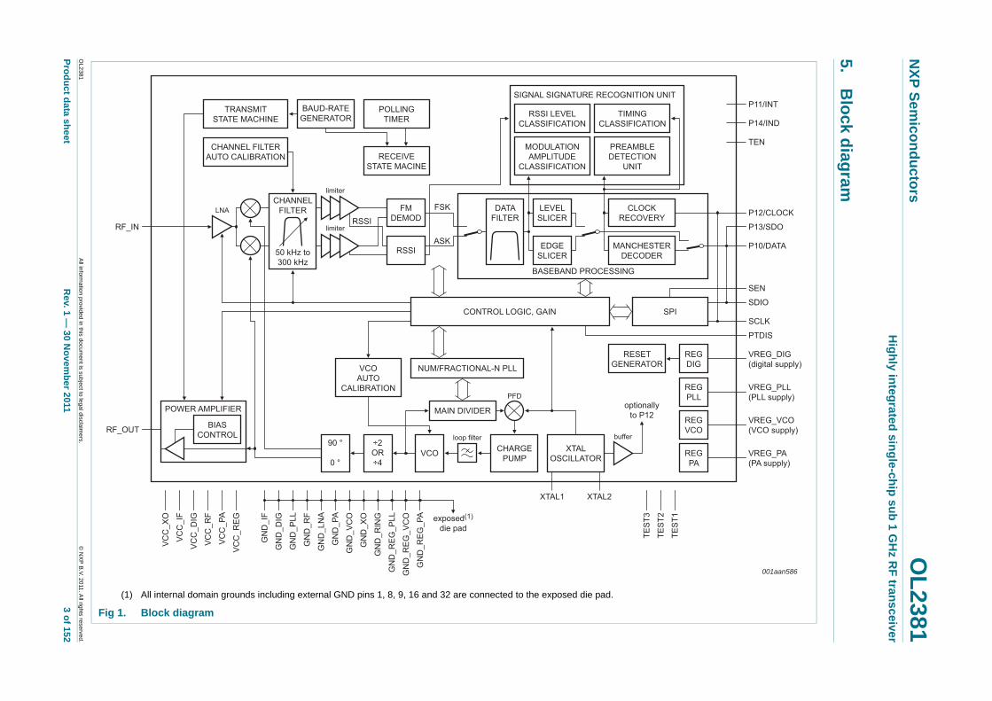
(1) All internal domain grounds including external GND pins 1, 8, 9, 16 and 32 are connected to the exposed die pad.
Fig 1. Block diagram
LNA
exposed(1)
die pad
RF_OUT
VC
C_X
O
RF_IN
XTAL1
CONTROL LOGIC, GAIN
NUM/FRACTIONAL-N PLL
MAIN DIVIDER
VCOAUTO
CALIBRATION
LEVELSLICER
DATAFILTER
EDGESLICER
RESETGENERATO
XTALOSCILLATOR
optionalto P12
CHARGEPUMP
BIASCONTROL
POWER AMPLIFIER
VCO÷2OR÷4
90 °
0 °
FMDEMOD
RSSI
RSSI
FSK
ASK
CLOCKRECOVE
MANCHESDECODE
BASEBAND PROCESSING
bufferloop filter
PFD
limiter
limiter
CHANNELFILTER
50 kHz to300 kHz
XTAL2
VC
C_I
F
VC
C_D
IG
VC
C_R
F
VC
C_P
A
VC
C_R
EG
GN
D_I
F
GN
D_D
IG
GN
D_P
LL
TES
T3
GN
D_R
F
GN
D_L
NA
GN
D_P
A
GN
D_V
CO
GN
D_X
O
GN
D_R
ING
GN
D_R
EG
_PLL
GN
D_R
EG
_VC
O
GN
D_R
EG
_PA
NXP Semiconductors OL2381Highly integrated single-chip sub 1 GHz RF transceiver
6. Pinning information
6.1 Pinning
6.2 Pin description
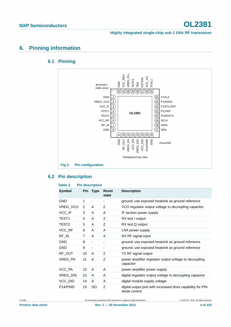
Fig 2. Pin configuration
001aan585
OL2381
Transparent top view
SEN
RF_IN
GND
SDIO
VCC_RF SCLK
TEST2 P10/DATA
TEST1 P11/INT
VCC_IF P12/CLOCK
VREG_VCO P13/SDO
GND XTAL2
GN
D
RF
_OU
T
VR
EG
_PA
VC
C_P
A
VR
EG
_DIG
VC
C_D
IG
P14
/PIN
D
GN
D
GN
D
VC
C_R
EG
VR
EG
_PLL
TE
ST
3
TE
N
RS
TD
IS
VC
C_X
O
XT
AL1
8 17
7 18
6 19
5 20
4 21
3 22
2 23
1 24
9 10 11 12 13 14 15 16
32 31 30 29 28 27 26 25
terminal 1index area
Table 2. Pin description
Symbol Pin Type Reset state
Description
GND 1 - - ground; use exposed heatsink as ground reference
VREG_VCO 2 A Z VCO regulator output voltage to decoupling capacitor
VCC_IF 3 A A IF section power supply
TEST1 4 A Z RX test I output
TEST2 5 A Z RX test Q output
VCC_RF 6 A A LNA power supply
RF_IN 7 A A RX RF signal input
GND 8 - - ground; use exposed heatsink as ground reference
GND 9 - - ground; use exposed heatsink as ground reference
RF_OUT 10 A Z TX RF signal output
VREG_PA 11 A Z power amplifier regulator output voltage to decoupling capacitor
VCC_PA 12 A A power amplifier power supply
VREG_DIG 13 A A digital regulator output voltage to decoupling capacitor
VCC_DIG 14 A A digital module supply voltage
P14/PIND 15 DO Z digital output port with increased drive capability for PIN diode control
OL2381 All information provided in this document is subject to legal disclaimers. © NXP B.V. 2011. All rights reserved.
Product data sheet Rev. 1 — 30 November 2011 4 of 152
NXP Semiconductors OL2381Highly integrated single-chip sub 1 GHz RF transceiver
[1] A = analog.
DI = digital input.
DO = digital output with enable signal.
DIO = digital input without enable signal and output with enable signal.
DIeO = digital input and output both with enable signal.
7. Functional description
7.1 General architecture description
The OL2381 transceiver is designed for use in both complex base-stations, when paired with powerful microcontrollers, and low component-count remote units with low pin-count microcontrollers. The IC features unique configuration possibilities via external pin-level configuration or SFR bit manipulation. Several automatic sequences are implemented to ease device operation, all of which can be manually influenced or overridden by control-bits.
GND 16 - - ground; use exposed heatsink as ground reference
SEN 17 DI DI serial interface enable
SDIO 18 DIO DI serial interface input/output
SCLK 19 DIO DI serial interface clock
P10/DATA 20 DIeO Z digital output port, TX data input, RX data output, data output of debug interface
P11/INT 21 DO POR, interrupt output
digital output port, interrupt output, several status indicators, reference clock output, frame indicator of debug interface
P12/CLOCK 22 DO 1 MHz reference clock
digital output port, TX/reference clock out, RX data clock, clock of debug interface
P13/SDO 23 DO Z digital output port, status indicators, serial interface data output
XTAL2 24 A A crystal reference clock frequency input
XTAL1 25 A A crystal connection
VCC_XO 26 A A crystal oscillator supply voltage
RSTDIS 27 DI DI reset disable signal
TEN 28 DI DI test enable input
TEST3 29 A Z PLL test output
VREG_PLL 30 A Z PLL regulator output voltage to decoupling capacitor
VCC_REG 31 A A PLL, VCO regulators power supply
GND 32 - - ground; use exposed heatsink as ground reference
exposed die pad
- A GND ground connection
Table 2. Pin description …continued
Symbol Pin Type Reset state
Description
OL2381 All information provided in this document is subject to legal disclaimers. © NXP B.V. 2011. All rights reserved.
Product data sheet Rev. 1 — 30 November 2011 5 of 152
NXP Semiconductors OL2381Highly integrated single-chip sub 1 GHz RF transceiver
7.1.1 Power management
The device contains a configurable power-on reset block. The device control registers are reset as the external voltage rises to ensure that the device state is in Standby mode. This is implemented by ensuring that all blocks are off except the SPI and the digital regulator. Note that the digital regulator is operating in clamp mode at this time.
7.1.2 XTAL oscillator
The main time-reference is derived from an amplitude-controlled XTAL oscillator. This 16 MHz reference is used as a reference clock for the PLL and as a timing reference for various analog calibration purposes.
7.1.3 Polling timer
Several base-station applications require a low-power polling timer for periodic device wakeup. This feature is essential to enable listening in pre-programmed time-windows when the OL2381 is used in RX mode applications. Internal configuration and trimming registers allow the setting of a wide range of different timer intervals while achieving an average timing accuracy of 2 %.
7.1.4 TX block
The TX section is able to operate within all ISM bands: 315 MHz, 434 MHz, 868 MHz and 916 MHz. The device provides a high degree of flexibility and is capable of ASK/FSK modulation, output power control and on-chip baud-rate generation with data rates up to 112 kchip/s. The device features multi-channel operation and enables carrier frequency adjustment and compensation of XTAL frequency offsets due to its high resolution fractional-N PLL architecture. The TX block features a high degree of integration, employing an on-chip VCO and PLL loop filter.
OL2381 All information provided in this document is subject to legal disclaimers. © NXP B.V. 2011. All rights reserved.
Product data sheet Rev. 1 — 30 November 2011 6 of 152

NXP Semiconductors OL2381Highly integrated single-chip sub 1 GHz RF transceiver
7.1.5 VCO calibration
On-chip calibration is available to reduce the VCO input voltage range and thus reduce the PLL loop bandwidth variation. The variation in system parameters such as locking time and LO phase noise can therefore be maintained within a tight window.
Calibration is performed by selecting the proper VCO sub-band according to the desired channel frequency. VCO sub-band selection and the PLL start-up sequence can be triggered by command and are supported by an automatic flow sequence. This flow can be overridden if required. Note that if the incorrect sub-band is chosen the VCO calibration is unable to tune to the desired frequency.
7.1.6 TX command
TX parameters (frequency, modulation, output power etc) can be predefined to enable fast and simple entry into TX mode (PA switched on).
Fig 3. TX block diagram
001aan587
/N /N+1
∑∆ MODULATOR
POWERCONTROL
TX/RXSWITCH
VCOCALIBRATION
VCO1.20 GHz -1.856 GHz
diff to SEbuffer
toRX mixer
analog part
PA 1 PA 2PA
÷2
/R2
0
1 ÷2
RF_LO_DIV
0
1
FSK/ASK
data in
UP3rd-orderloop filter
DOWN
PFD
referenceoscillator
chargepump
main divider
DIGITAL PART
N integer
FSK FILTER
LATCH
N Fract
K Fdev
/R1
OL2381 All information provided in this document is subject to legal disclaimers. © NXP B.V. 2011. All rights reserved.
Product data sheet Rev. 1 — 30 November 2011 7 of 152
NXP Semiconductors OL2381Highly integrated single-chip sub 1 GHz RF transceiver
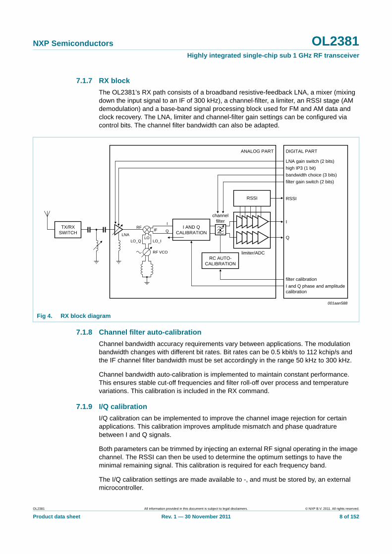
7.1.7 RX block
The OL2381’s RX path consists of a broadband resistive-feedback LNA, a mixer (mixing down the input signal to an IF of 300 kHz), a channel-filter, a limiter, an RSSI stage (AM demodulation) and a base-band signal processing block used for FM and AM data and clock recovery. The LNA, limiter and channel-filter gain settings can be configured via control bits. The channel filter bandwidth can also be adapted.
7.1.8 Channel filter auto-calibration
Channel bandwidth accuracy requirements vary between applications. The modulation bandwidth changes with different bit rates. Bit rates can be 0.5 kbit/s to 112 kchip/s and the IF channel filter bandwidth must be set accordingly in the range 50 kHz to 300 kHz.
Channel bandwidth auto-calibration is implemented to maintain constant performance. This ensures stable cut-off frequencies and filter roll-off over process and temperature variations. This calibration is included in the RX command.
7.1.9 I/Q calibration
I/Q calibration can be implemented to improve the channel image rejection for certain applications. This calibration improves amplitude mismatch and phase quadrature between I and Q signals.
Both parameters can be trimmed by injecting an external RF signal operating in the image channel. The RSSI can then be used to determine the optimum settings to have the minimal remaining signal. This calibration is required for each frequency band.
The I/Q calibration settings are made available to -, and must be stored by, an external microcontroller.
Fig 4. RX block diagram
001aan588
TX/RXSWITCH
I AND QCALIBRATION
RC AUTO-CALIBRATION
RSSI
limiter/ADC
ANALOG PART DIGITAL PART
LNA gain switch (2 bits)
high IP3 (1 bit)
bandwidth choice (3 bits)
filter gain switch (2 bits)
RSSI
I
Q
I and Q phase and amplitudecalibration
filter calibration
channelfilter
LNALO
IF
I
Q
LO_Q LO_I
RF VCO
RF
OL2381 All information provided in this document is subject to legal disclaimers. © NXP B.V. 2011. All rights reserved.
Product data sheet Rev. 1 — 30 November 2011 8 of 152
NXP Semiconductors OL2381Highly integrated single-chip sub 1 GHz RF transceiver
7.1.10 Receive command
The predefined set of RX parameters (center frequency, modulation, etc.) enables Receive mode (receiver and LO buffers switched on) to be entered quickly after receiving the RX command. Several methods of signal signature recognition are implemented. These modes of semi-automatic signal processing can be pre-selected by the RX command.
7.1.11 Signal signature recognition unit
Several signal recognition units are implemented to provide fast and accurate signal detection. Signal signatures such as signal level (RSSI), modulation depth or baud-rate and coding can be automatically detected as wakeup criteria during the wakeup search phase.
7.1.12 Preamble detection
A configurable 1-bit to 32-bit pattern recognition unit can be implemented to aid power saving and avoid unintended wakeup due to ambient noise.
7.2 General operation
The OL2381 is a state machine-based transceiver to be used in conjunction with a microcontroller. Study this datasheet carefully to help choose the appropriate OL2381 configuration for a specific application. The interface to the microcontroller must be defined first, see Section 7.3. Next, the correct basic settings must be identified. The operational frequency band must be chosen, all relevant registers must be programmed for TX and RX modes (exact setting of desired frequency, modulation, modulation depth, IF bandwidth, baseband filtering, etc). It is strongly recommended to study every aspect of this datasheet in detail and to verify correct device operation by measuring available debug-signals. The optimum operation and the highest device performance is achieved by fine-tuning and verification of all device settings. Use the automatic operating sequences after determining the optimum device configuration. Generally, the first operation is to bring the device from standby to power-up state, which is the precondition for any operation. This can be done manually, triggered by the external microcontroller, or automatically by the built-in polling timer. In this device mode, the XTAL oscillator is operational. SFR register bits (configuration data) can be changed. This mode can be left by issuing TX or RX commands. To save power and operating time the commands can be prepared by the ‘prepare TX’ or ‘prepare RX’ commands.
7.3 Interface description
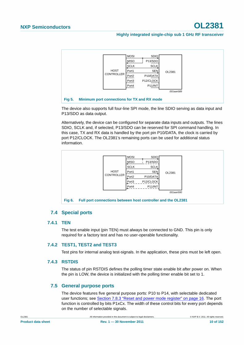
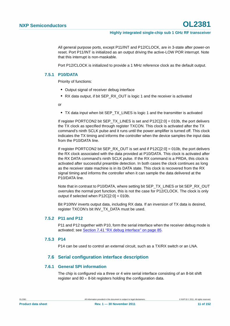
7.3.1 Port connections
The minimum connection between a host controller and the OL2381 comprises three SPI lines: SDIO, SCLK and SEN. SPI communication and TX/RX data transfer can be achieved by multiplexing the SPI data and clock lines. The host controller’s SPI must be set in slave mode after the RX/TX command is sent, the SCKL then shifts the out/in data via the host controller’s SPI.
OL2381 All information provided in this document is subject to legal disclaimers. © NXP B.V. 2011. All rights reserved.
Product data sheet Rev. 1 — 30 November 2011 9 of 152
NXP Semiconductors OL2381Highly integrated single-chip sub 1 GHz RF transceiver
The device also supports full four-line SPI mode, the line SDIO serving as data input and P13/SDO as data output.
Alternatively, the device can be configured for separate data inputs and outputs. The lines SDIO, SCLK and, if selected, P13/SDO can be reserved for SPI command handling. In this case, TX and RX data is handled by the port pin P10/DATA, the clock is carried by port P12/CLOCK. The OL2381’s remaining ports can be used for additional status information.
7.4 Special ports
7.4.1 TEN
The test enable input (pin TEN) must always be connected to GND. This pin is only required for a factory test and has no user-operable functionality.
7.4.2 TEST1, TEST2 and TEST3
Test pins for internal analog test-signals. In the application, these pins must be left open.
7.4.3 RSTDIS
The status of pin RSTDIS defines the polling timer state enable bit after power on. When the pin is LOW, the device is initialized with the polling timer enable bit set to 1.
7.5 General purpose ports
The device features five general purpose ports: P10 to P14, with selectable dedicated user functions; see Section 7.8.3 “Reset and power mode register” on page 16. The port function is controlled by bits P1xCx. The width of these control bits for every port depends on the number of selectable signals.
Fig 5. Minimum port connections for TX and RX mode
Fig 6. Full port connections between host controller and the OL2381
001aan589
MOSI
HOSTCONTROLLER
OL2381
MISO
SCLK
Port1
Port2
Port3
Port4
SDIO
P13/SDO
SCLK
SEN
P10/DATA
P12/CLOCK
P11/INT
001aan590
MOSI
HOSTCONTROLLER
OL2381
MISO
SCLK
Port1
Port2
Port3
Port4
SDIO
P13/SDO
SCLK
SEN
P10/DATA
P12/CLOCK
P11/INT
OL2381 All information provided in this document is subject to legal disclaimers. © NXP B.V. 2011. All rights reserved.
Product data sheet Rev. 1 — 30 November 2011 10 of 152
NXP Semiconductors OL2381Highly integrated single-chip sub 1 GHz RF transceiver
All general purpose ports, except P11/INT and P12/CLOCK, are in 3-state after power-on reset. Port P11/INT is initialized as an output driving the active-LOW POR interrupt. Note that this interrupt is non-maskable.
Port P12/CLOCK is initialized to provide a 1 MHz reference clock as the default output.
7.5.1 P10/DATA
Priority of functions:
• Output signal of receiver debug interface
• RX data output, if bit SEP_RX_OUT is logic 1 and the receiver is activated
or
• TX data input when bit SEP_TX_LINES is logic 1 and the transmitter is activated
If register PORTCON2 bit SEP_TX_LINES is set and P12C[2:0] = 010b, the port delivers the TX clock as specified through register TXCON. This clock is activated after the TX command’s ninth SCLK pulse and it runs until the power amplifier is turned off. This clock indicates the TX timing and informs the controller when the device samples the input data from the P10/DATA line.
If register PORTCON2 bit SEP_RX_OUT is set and if P12C[2:0] = 010b, the port delivers the RX clock associated with the data provided at P10/DATA. This clock is activated after the RX DATA command’s ninth SCLK pulse. If the RX command is a PRDA, this clock is activated after successful preamble detection. In both cases the clock continues as long as the receiver state machine is in its DATA state. This clock is recovered from the RX signal timing and informs the controller when it can sample the data delivered at the P10/DATA line.
Note that in contrast to P10/DATA, where setting bit SEP_TX_LINES or bit SEP_RX_OUT overrules the normal port function, this is not the case for P12/CLOCK. The clock is only output if selected when P12C[2:0] = 010b.
Bit P10INV inverts output data, including RX data. If an inversion of TX data is desired, register TXCON’s bit INV_TX_DATA must be used.
7.5.2 P11 and P12
P11 and P12 together with P10, form the serial interface when the receiver debug mode is activated; see Section 7.41 “RX debug interface” on page 85.
7.5.3 P14
P14 can be used to control an external circuit, such as a TX/RX switch or an LNA.
7.6 Serial configuration interface description
7.6.1 General SPI information
The chip is configured via a three or 4 wire serial interface consisting of an 8-bit shift register and 80 8-bit registers holding the configuration data.
OL2381 All information provided in this document is subject to legal disclaimers. © NXP B.V. 2011. All rights reserved.
Product data sheet Rev. 1 — 30 November 2011 11 of 152
NXP Semiconductors OL2381Highly integrated single-chip sub 1 GHz RF transceiver
Data can be exchanged with multiple 8-bit frames (auto-incrementing) or in portions of 8 bits (1 byte), which provides an advantage when using a hardware SPI-interface. Data in the shift register is loaded into the addressed register on the last edge of SCLK within the last bit of the transferred byte.
7.6.2 SEN
A logic LOW applied to pin SEN disables the SPI interface. The internal state machine halts and every activity on pins SDIO and SCLK is ignored.
If the device is in Power-down mode, a positive edge on pin SEN activates the device. The crystal oscillator is always on, unless the device is in Power-down mode. The watchdog is cleared with a HIGH level on pin SEN; see Section 7.11 “Watchdog” on page 25.
After the TX command, pin SEN has an additional function: At the falling edge of pin SEN the level on pin SDIO is latched and frozen.
7.6.3 SCLK
SCLK is the clock pin for the serial interface. Every edge of SCLK shifts data into or gets data from the SPI register-set. The second clock edge (SCLK) is used for data capturing. SDIO direction switching between input and output is accomplished with the first clock edge of the ninth bit. An additional clock edge is necessary at the start of a TX or RX command.
The clock polarity for an SPI command can be selected; see Section 7.6.5.
If desired, pin SCLK can carry the baud-rate clock during a TX command and the recovered RX clock during a RX command.
7.6.4 SDIO
SDIO is the serial interface’s bidirectional data input/output pin. Data in or data out operation is adapted automatically during SPI communication sequences.
If desired, pin SDIO can be used to input data if a TX command is executed or for RX data if a RX command is active.
7.6.5 General SFR access information
If SCLK is HIGH at the rising edge of SEN, the data is transferred with the rising edge of SCLK; see Figure 7 and Figure 8. If SCLK is LOW at the rising edge of SEN, the data is transferred at the falling edge of SCLK.
For continuity, all figures and examples in this data sheet assume SEN is LOW at the rising edge of SCLK, unless otherwise stated. The first edge of SCLK is referred to as the rising edge and the second as the falling edge.
OL2381 All information provided in this document is subject to legal disclaimers. © NXP B.V. 2011. All rights reserved.
Product data sheet Rev. 1 — 30 November 2011 12 of 152
NXP Semiconductors OL2381Highly integrated single-chip sub 1 GHz RF transceiver
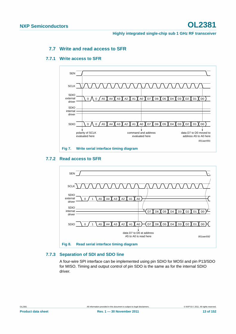
7.7 Write and read access to SFR
7.7.1 Write access to SFR
7.7.2 Read access to SFR
7.7.3 Separation of SDI and SDO line
A four-wire SPI interface can be implemented using pin SDIO for MOSI and pin P13/SDO for MISO. Timing and output control of pin SDO is the same as for the internal SDIO driver.
Fig 7. Write serial interface timing diagram
SEN
SCLK
SDIOexternal
driver0
SDIOinternal
driver
A5 A4 A3 A2 A1 A0 D7 D6 D5 D4 D3 D2 D1 D0
data D7 to D0 moved toaddress A5 to A0 here
0
SDIO 0 A5 A4 A3 A2 A1 A0 D7 D6 D5 D4 D3 D2 D1 D00
001aan591
command and addressevaluated here
polarity of SCLKevaluated here
Fig 8. Read serial interface timing diagram
SEN
SCLK
SDIOexternal
driver
SDIOinternal
driver
data D7 to D0 at addressA5 to A0 is read here
SDIO 0 A5 A4 A3 A2 A1 A0 D7 D6 D5 D4 D3 D2 D1 D01
001aan592
0 A5 A4 A3 A2 A1 A01
D7 D6 D5 D4 D3 D2 D1 D0
OL2381 All information provided in this document is subject to legal disclaimers. © NXP B.V. 2011. All rights reserved.
Product data sheet Rev. 1 — 30 November 2011 13 of 152

NXP Semiconductors OL2381Highly integrated single-chip sub 1 GHz RF transceiver
7.7.4 Read access to SFR with separate SDO line
7.7.5 Read and write access to SFR with auto-increment function
If the SPI clock (SCLK) is still applied after the first 8 data bits are transferred, the auto-increment function automatically increments the address by one for the following 8 data bits. This enables data to be written to a continuous range of bytes without having to set the address for every single data-byte. The auto-increment function is terminated on the falling edge of SEN.
If the address reaches the end of the address range (3Fh) an additional increment causes the address to start at 00h again. This wrap around is accomplished in the current address bank. The auto-increment function has no influence on the bank selection.
Fig 9. Read serial interface timing diagram (SEP_SDO = 1)
SEN
SCLK
SDIOexternal
driver
data D7 to D0 at addressA5 to A0 is read here
SDIO 0 A5 A4 A3 A2 A1 A01
001aan593
0 A5 A4 A3 A2 A1 A01
SDIOinternal
driver
P13/SDIO D7 D6 D5 D4 D3 D2 D1 D0
OL2381 All information provided in this document is subject to legal disclaimers. © NXP B.V. 2011. All rights reserved.
Product data sheet Rev. 1 — 30 November 2011 14 of 152
xxxxxxxxxxxxxxxxxxxxx xxxxxxxxxxxxxxxxxxxxxxxxxx xxxxxxx x x x xxxxxxxxxxxxxxxxxxxxxxxxxxxxxx xxxxxxxxxxxxxxxxxxx xx xx xxxxx xxxxxxxxxxxxxxxxxxxxxxxxxxx xxxxxxxxxxxxxxxxxxx xxxxxx xxxxxxxxxxxxxxxxxxxxxxxxxxxxxxxxxxx xxxxxxxxxxxx x x xxxxxxxxxxxxxxxxxxxxx xxxxxxxxxxxxxxxxxxxxxxxxxxxxxx xxxxx xxxxxxxxxxxxxxxxxxxxxxxxxxxxxxxxxxxxxxxxxxxxxxxxxx xxxxxxxx xxxxxxxxxxxxxxxxxxxxxxxxx xxxxxxxxxxxxxxxxxxxx xxx
OL2
381
Pro
du
ct data sh
NX
P S
emico
nd
ucto
rsO
L2381
Hig
hly
integ
rate
d sin
gle-ch
ip su
b 1
GH
z RF
tran
sc
eiver
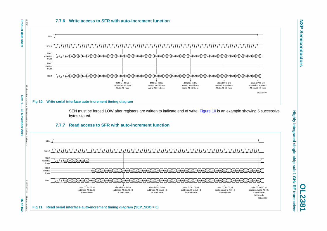
7.7.6 Write access to SFR with auto-increment function
is an example showing 5 successive
SEN
001aan594
data D7 to D0moved to addressA5 to A0 +4 here
data D7 to D0moved to addressA5 to A0 +3 here
2 D1 D0 D7 D6 D5 D4 D3 D2 D1 D0
2 D1 D0 D7 D6 D5 D4 D3 D2 D1 D0
001aan595
data D7 to D0 ataddress A5 to A0 +5
is read here(not used)
data D7 to D0 atddress A5 to A0 +4
is read here
2 D1 D0 D7 D6 D5 D4 D3 D2 D1 D0
2 D1 D0 D7 D6 D5 D4 D3 D2 D1 D0
All inform
ation provided in this docum
ent is subject to legal disclaim
ers.©
NX
P B
.V. 20
11. All rights reserved
.
eetR
ev. 1 — 30 N
ovem
ber 2011
15 of 15
2
SEN must be forced LOW after registers are written to indicate end of write. Figure 10bytes stored.
7.7.7 Read access to SFR with auto-increment function
Fig 10. Write serial interface auto-increment timing diagram
SDIOexternal
driver
SCLK
data D7 to D0moved to addressA5 to A0 +2 here
data D7 to D0moved to addressA5 to A0 +1 here
data D7 to D0moved to address
A5 to A0 here
0 0 A5 A4 A3 A2 A1 A0 D7 D6 D5 D4 D3 D2 D1 D0 D7 D6 D5 D4 D3 D2 D1 D0 D7 D6 D5 D4 D3 D2 D1 D0 D7 D6 D5 D4 D3 D
SDIOinternal
driver
0 0 A5 A4 A3 A2 A1 A0 D7 D6 D5 D4 D3 D2 D1 D0 D7 D6 D5 D4 D3 D2 D1 D0 D7 D6 D5 D4 D3 D2 D1 D0 D7 D6 D5 D4 D3 DSDIO
Fig 11. Read serial interface auto-increment timing diagram (SEP_SDO = 0)
SDIOexternal
driver
SCLK
SEN
adata D7 to D0 at
address A5 to A0 +3is read here
data D7 to D0 ataddress A5 to A0 +2
is read here
data D7 to D0 ataddress A5 to A0 +1
is read here
data D7 to D0 ataddress A5 to A0
is read here
0 1 A5 A4 A3 A2 A1 A0
0 1 A5 A4 A3 A2 A1 A0
SDIOinternal
driver
D7 D6 D5 D4 D3 D2 D1 D0 D7 D6 D5 D4 D3 D2 D1 D0 D7 D6 D5 D4 D3 D2 D1 D0 D7 D6 D5 D4 D3 D
D7 D6 D5 D4 D3 D2 D1 D0 D7 D6 D5 D4 D3 D2 D1 D0 D7 D6 D5 D4 D3 D2 D1 D0 D7 D6 D5 D4 D3 D
SDIO
NXP Semiconductors OL2381Highly integrated single-chip sub 1 GHz RF transceiver
SEN must be forced LOW after registers are read to indicate end of read. Figure 11 is an example showing 5 successive bytes read.
7.8 Device mode description
7.8.1 Automatic start-up procedures
The device features the following automatic start-up procedures for easy device handling and configuration:
• Power-on and crystal oscillator start-up
• PLL and VCO start-up including calibration
• Preparation for TX mode
• Preparation for RX mode
• VCO auto-calibration at every center frequency change
7.8.2 General description
The automatic start-up procedures are implemented to aid the quick and easy transition between operational states. Most procedures are controlled by changing bits in the PWRMODE register. Certain configurations can be directly entered by the TX or RX commands.
7.8.3 Reset and power mode register
The PWRMODE register acts as the device’s ‘main power on/off/standby switch’. Setting the RESET bit of this register brings the device into the reset condition equal to the power-on reset state. This power-down state is also reached automatically at first power-on (battery insertion). If this bit is set with a write command, the effect on all registers with a reset condition is a ‘hard-reset’. If, with the same SPI write command, other bits are simultaneously written to the PWRMODE register, they are changed automatically to the power-on reset state; see Section 8.2.1.10 “General power mode register PWRMODE” on page 100.
7.8.3.1 First power-on reset
The non-maskable interrupt flag IF_POR is set when the initial power-on reset takes place (battery insertion).
7.8.3.2 Power-down
Setting bit PD brings the device into low current consumption standby mode. All analog receiver and transmitter circuitry including the crystal oscillator are turned off and all dynamic digital activity is stopped. Only the SPI and the polling timer, if enabled, are active. Bit PD is also under automatic device control and is set under the following conditions:
• power-on reset or setting bit RESET (setting bit RESET overrides all others)
• the watchdog timer times out
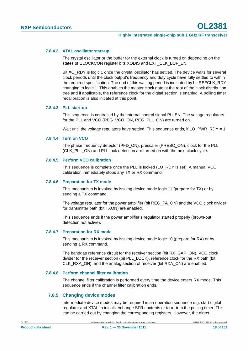
7.8.3.3 Device mode states
Three important static device internal enable signals are decoded from DEV_MODE: PLLEN, TXEN and RXEN.
OL2381 All information provided in this document is subject to legal disclaimers. © NXP B.V. 2011. All rights reserved.
Product data sheet Rev. 1 — 30 November 2011 16 of 152
NXP Semiconductors OL2381Highly integrated single-chip sub 1 GHz RF transceiver
• PLLEN is set whenever the DEV_MODE is not logic 00
• RXEN is set only if DEV_MODE is logic 10
• TXEN is set only if DEV_MODE is logic 11
An important implication of this is that a TX operation is immediately aborted if the active mode is switched to anything except TX mode, for example, switching the device into RX mode immediately shuts down the power amplifier without smoothly ramping down the RF power.
Conversely, entering TX mode immediately aborts any RX operation.
DEV_MODE bits can be either set directly by writing the PWRMODE register or by sending a RX or a TX command, where a RX command sets DEV_MODE to logic 10 and a TX command sets DEV_MODE to logic 11.
Setting bit RESET or setting bit PD (power-down) resets DEV_MODE to logic 00, where only the crystal oscillator is (potentially) enabled.
An alternative to setting the device mode can be to send a TX command and delay the ‘9th edge’. This sets the frequency and initiates the device as if in TX mode. The PA is then switched on at the TX command’s 9th edge.
7.8.4 Flow description
The following actions are performed if the device leaves power-down state and enters active state. The internal control signals of these states are explained in more detail in later sections.
Power-down state indicator is cleared.
7.8.4.1 Digital regulator start-up
The digital voltage regulator is turned on whenever the device leaves the power-down state.
Fig 12. Simplified state diagram
001aan596
TRANSMIT STATE
IDLE STATE
TX commandSPI command
RECEIVE STATE
preparereceiver = 1
pollingtimerevent
power-downconditions
SEN = 1
SPI command
RX commandSPI command
preparereceiver = 0
POWER-DOWNSTATE
preparetransmitter = 1
power-downconditions
power-downconditions
RX command
TX command
preparetransmitter = 0
power-onreset
OL2381 All information provided in this document is subject to legal disclaimers. © NXP B.V. 2011. All rights reserved.
Product data sheet Rev. 1 — 30 November 2011 17 of 152
NXP Semiconductors OL2381Highly integrated single-chip sub 1 GHz RF transceiver
7.8.4.2 XTAL oscillator start-up
The crystal oscillator or the buffer for the external clock is turned on depending on the states of CLOCKCON register bits XODIS and EXT_CLK_BUF_EN.
Bit XO_RDY is logic 1 once the crystal oscillator has settled. The device waits for several clock periods until the clock output’s frequency and duty cycle have fully settled to within the required specification. The end of this waiting period is indicated by bit REFCLK_RDY changing to logic 1. This enables the master clock gate at the root of the clock distribution tree and if applicable, the reference clock for the digital section is enabled. A polling timer recalibration is also initiated at this point.
7.8.4.3 PLL start-up
This sequence is controlled by the internal control signal PLLEN. The voltage regulators for the PLL and VCO (REG_VCO_ON, REG_PLL_ON) are turned on.
Wait until the voltage regulators have settled. This sequence ends, if LO_PWR_RDY = 1.
7.8.4.4 Turn on VCO
The phase frequency detector (PFD_ON), prescaler (PRESC_ON), clock for the PLL (CLK_PLL_ON) and PLL lock detection are turned on with the next clock cycle.
7.8.4.5 Perform VCO calibration
This sequence is complete once the PLL is locked (LO_RDY is set). A manual VCO calibration immediately stops any TX or RX command.
7.8.4.6 Preparation for TX mode
This mechanism is invoked by issuing device mode logic 11 (prepare for TX) or by sending a TX command.
The voltage regulator for the power amplifier (bit REG_PA_ON) and the VCO clock divider for transmitter path (bit TXON) are enabled.
This sequence ends if the power amplifier’s regulator started properly (brown-out detection not active).
7.8.4.7 Preparation for RX mode
This mechanism is invoked by issuing device mode logic 10 (prepare for RX) or by sending a RX command.
The bandgap reference circuit for the receiver section (bit RX_GAP_ON), VCO clock divider for the receiver section (bit PLL_LOCK), reference clock for the RX path (bit CLK_RXA_ON), and the analog section of receiver (bit RXA_ON) are enabled.
7.8.4.8 Perform channel filter calibration
The channel filter calibration is performed every time the device enters RX mode. This sequence ends if the channel filter calibration ends.
7.8.5 Changing device modes
Intermediate device modes may be required in an operation sequence e.g. start digital regulator and XTAL to initialize/change SFR contents or to re-trim the polling timer. This can be carried out by changing the corresponding registers. However, the direct
OL2381 All information provided in this document is subject to legal disclaimers. © NXP B.V. 2011. All rights reserved.
Product data sheet Rev. 1 — 30 November 2011 18 of 152
NXP Semiconductors OL2381Highly integrated single-chip sub 1 GHz RF transceiver
commands may be more useful if the only operation required is the entering of TX or RX mode. The corresponding sequences start automatically and operation enabled after all internal settling times are met.
7.8.6 Interrupts
TheOL2381 can generate various interrupts which can be enabled by the IEN register and read from the IFLAG register; see Section 8.2.1.11 “Interrupt enable register IEN” on page 101. The IFLAG register is always cleared after it is read. Certain pins can also be configured to present these interrupts; see Section 7.3 “Interface description” on page 9.
7.9 Power supply and reset
Each main functional block is equipped with its own dedicated supply voltage pin. Therefore, several supply pins are available on the package and all must be connected. Note that all ground connections of these functional blocks are bonded to the exposed die pad of the package (metal plate underneath the die). Some blocks are supplied via dedicated integrated low-dropout voltage-regulators. Note that for all regulators the output voltage is available both internally and externally on a pin for connection of a decoupling capacitor. The following blocks have regulated supplies.
7.9.1 Voltage regulators operation
All regulators are operated automatically by selecting the corresponding device modes. The device modes are set by DEV_MODE[1:0] in register PWRMODE; for details see Section 7.8.3 “Reset and power mode register” on page 16.
The regulators can also be independently controlled by the control bits located inside the TEST registers. Individual operation of the voltage regulators can be necessary for debug or measurement purposes. The following paragraphs describe each individual regulator and its purpose.
7.9.2 Digital regulator
Before the device can be operated, the digital regulator must be switched on. In standby state (power-down state) the digital regulator is bypassed and supplies the digital section with a low supply voltage to guarantee data retention in the configuration registers. If the digital regulator is switched on, the voltage reaches its stabilized value of approximately 1.8 V. The digital regulator can be activated or deactivated by bit REG_DIG_DIS in TEST1 register. Clearing the bit enables the regulator, depending on the selected device mode. Setting the bit always disables the regulator.
7.9.3 PLL regulator
To start any PLL operation the PLL regulator must be switched on. This happens automatically with operation of bit REG_PLL_ON in the TEST2 register.
Table 3. Blocks with regulated supplies
Block Regulator supply pin Pin to decouple
PLL VCC_REG VREG_PLL
VCO VCC_REG VREG_VCO
PA VCC_PA VREG_PA
digital VCC_DIG VREG_DIG
OL2381 All information provided in this document is subject to legal disclaimers. © NXP B.V. 2011. All rights reserved.
Product data sheet Rev. 1 — 30 November 2011 19 of 152

NXP Semiconductors OL2381Highly integrated single-chip sub 1 GHz RF transceiver
Remark: this bit only starts the PLL regulator, all PLL functional blocks are enabled individually by separate control-bits.
7.9.4 VCO regulator
For stability and immunity reasons the VCO is supplied via an independent voltage regulator. This regulator can be manually controlled via bit REG_VCO_ON in the TEST2 register.
Remark: this bit only starts the VCO regulator. VCO operation is enabled individually by a separate control-bit.
7.9.5 PA regulator
This regulator is enabled if PA operation is desired. This can be manually controlled by setting bit REG_PA_ON.
Remark: this bit only starts the PA regulator. TX operation must be enabled by setting the corresponding command on the SPI interface.
7.9.6 Device reset
A device reset occurs whenever the supply voltage is applied on the VCC pins (battery insertion). The device utilizes two power-on detection mechanisms, one digital and one analog. These reset circuits constantly monitor the supply voltage. Setting bit RESET in the PWRMODE register performs the same operation by software. This is equivalent to a power-on reset. If bit RESET is set via a command, it is cleared automatically when SPI signal SEN goes LOW after the next write register command.
7.10 Main control and timing blocks
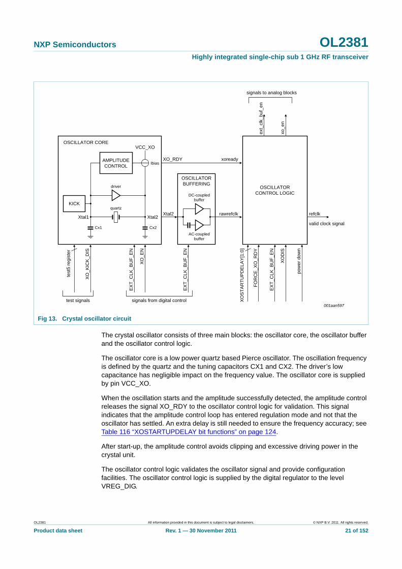
7.10.1 Crystal oscillator
7.10.1.1 Circuit description
The crystal oscillator is the source of the reference clock for the PLL, the digital section and the mixed signal blocks in the receiver chain. The crystal oscillator circuit diagram is shown in Figure 13.
OL2381 All information provided in this document is subject to legal disclaimers. © NXP B.V. 2011. All rights reserved.
Product data sheet Rev. 1 — 30 November 2011 20 of 152
NXP Semiconductors OL2381Highly integrated single-chip sub 1 GHz RF transceiver
The crystal oscillator consists of three main blocks: the oscillator core, the oscillator buffer and the oscillator control logic.
The oscillator core is a low power quartz based Pierce oscillator. The oscillation frequency is defined by the quartz and the tuning capacitors CX1 and CX2. The driver’s low capacitance has negligible impact on the frequency value. The oscillator core is supplied by pin VCC_XO.
When the oscillation starts and the amplitude successfully detected, the amplitude control releases the signal XO_RDY to the oscillator control logic for validation. This signal indicates that the amplitude control loop has entered regulation mode and not that the oscillator has settled. An extra delay is still needed to ensure the frequency accuracy; see Table 116 “XOSTARTUPDELAY bit functions” on page 124.
After start-up, the amplitude control avoids clipping and excessive driving power in the crystal unit.
The oscillator control logic validates the oscillator signal and provide configuration facilities. The oscillator control logic is supplied by the digital regulator to the level VREG_DIG.
Fig 13. Crystal oscillator circuit
001aan597
AMPLITUDECONTROL
KICK
test
5 re
gist
er
XO
ST
AR
TU
PD
ELA
Y[1
:0]
XO
_KIC
K_D
IS
FO
RC
E_X
O_R
DY
EX
T_C
LK_B
UF
_EN
XO
DIS
pow
er d
own
EX
T_C
LK_B
UF
_EN
EX
T_C
LK_B
UF
_EN
XO_RDY xoready
rawrefclk
XO
_EN
Xtal1
test signals
Xtal2Xtal2
VCC_XOOSCILLATOR CORE
Ibias
driver
Cx1 Cx2
quartz
refclk
valid clock signal
ext_
clk_
buf_
en
xo_e
n
DC-coupledbuffer
AC-coupledbuffer
OSCILLATORCONTROL LOGIC
OSCILLATORBUFFERING
signals from digital control
signals to analog blocks
OL2381 All information provided in this document is subject to legal disclaimers. © NXP B.V. 2011. All rights reserved.
Product data sheet Rev. 1 — 30 November 2011 21 of 152

NXP Semiconductors OL2381Highly integrated single-chip sub 1 GHz RF transceiver
The oscillator buffer consists of two amplifiers connected in parallel: one low-noise AC-coupled amplifier for crystal operation and one high-input voltage DC-coupled amplifier for testing purposes only. The buffer plays the role of level-shifter for the signals in PLL and digital supply domains. The buffer circuitry is supplied by the PLL and digital regulators accordingly.
Alternatively, an external clock signal can be applied at pin XTAL2; see the external clock buffer description in Section 7.10.2 “Oscillator control and control bits” on page 23. The applied signal must comply with the logic levels in the digital core (0 V for LOW and 1.8 V for HIGH). With the OL2381 properly configured, the DC-coupled amplifier replaces the low-noise AC-coupled amplifier. This provides the possibility to skip the internal oscillator’s start-up sequence and also allows the customer to stop the clock sequence for test purposes.
Remark: The use of an external clock signal requires special care in the hardware configuration. The oscillator core circuitry connected to pin XTAL2 cannot withstand levels higher than 2.8 V. Therefore, the use of this test mode with supply voltages higher than 2.8 V requires a hardware modification for pin VCC_XO. The recommended solution is to connect pin VCC_XO to pin VREG_DIG. In that configuration the circuit’s integrity is ensured but the digital noise needs to be considered.
The crystal oscillator is always active either in oscillator mode or in external clock buffer mode when the device is not in Power-down state.
OL2381 All information provided in this document is subject to legal disclaimers. © NXP B.V. 2011. All rights reserved.
Product data sheet Rev. 1 — 30 November 2011 22 of 152

xxxxxxxxxxxxxxxxxxxxx xxxxxxxxxxxxxxxxxxxxxxxxxx xxxxxxx x x x xxxxxxxxxxxxxxxxxxxxxxxxxxxxxx xxxxxxxxxxxxxxxxxxx xx xx xxxxx xxxxxxxxxxxxxxxxxxxxxxxxxxx xxxxxxxxxxxxxxxxxxx xxxxxx xxxxxxxxxxxxxxxxxxxxxxxxxxxxxxxxxxx xxxxxxxxxxxx x x xxxxxxxxxxxxxxxxxxxxx xxxxxxxxxxxxxxxxxxxxxxxxxxxxxx xxxxx xxxxxxxxxxxxxxxxxxxxxxxxxxxxxxxxxxxxxxxxxxxxxxxxxx xxxxxxxx xxxxxxxxxxxxxxxxxxxxxxxxx xxxxxxxxxxxxxxxxxxxx xxx
OL2
381
Pro
du
ct data sh
NX
P S
emico
nd
ucto
rsO
L2381
Hig
hly
integ
rate
d sin
gle-ch
ip su
b 1
GH
z RF
tran
sc
eiver
control bits in the OL2381’s register . Lower case signal names denote
ode and the external clock buffer e. The transition control ensures that buffer is turned on when the device is t; see Section 8.2.1.15 “Clock
in power-down mode disables all clock buffer on.
001aan598
OSCILLATORCORE ANDBUFFERING
TRANSITIONCONTROL
CLOCK GATE
en
ref_clk
REFCLK_RDY(1)
enxo_enableraw
xo_enablepower-downXODIS
clock_present
rdy
xtal1 xtal2
XO_RDY(1)
osc out
CP
D Q
R
All inform
ation provided in this docum
ent is subject to legal disclaim
ers.©
NX
P B
.V. 20
11. All rights reserved
.
eetR
ev. 1 — 30 N
ovem
ber 2011
23 of 15
2
7.10.2 Oscillator control and control bits
The oscillator control logic is described in Figure 14. Upper case signal names denoteset. Upper case signal names labeled ‘(1)’ denote (internal and ‘official’) status signalsinternal signals.
The enable logic is visible at the top left corner for both modes: the crystal oscillator mmode. The crystal oscillator is turned on when both, power-down and XODIS, are falsno glitches can be generated when turning the oscillator on and off. The external clocknot in power-down mode and both control bits, XODIS and EXT_CLK_BUF_EN are seconnection register CLOCKCON” on page 103. As a consequence, putting the deviceclock activity, and turning the crystal oscillator on has priority over turning the external
(1) Denote internal and official status signals.
Fig 14. Diagram for crystal oscillator with clock selection circuitry
TRANSITIONCONTROL
DELAYCOUNTER
ext_clk_buf_en
raw_ref_clk
raw ext_clk_buf_en
CPexpired
reset
XO_RDY(1)
power-down
FORCE_XO_RDY
EXT_CLK_BUF_EN
EXT_CLK_BUF_ENFORCE_XO_RDY
xo_enable
XO_RDY(1)
FORCE_XO_RDY
EXT_CLK_BUF_EN
pin XTAL1 pin XTAL2
delay ctrl
XOSTARTUPDELAY

NXP Semiconductors OL2381Highly integrated single-chip sub 1 GHz RF transceiver
If the crystal oscillator is turned on (XO_ENABLE becomes true) and a crystal is connected to the oscillator, the raw clock becomes available after the oscillation reaches a significant amplitude, which is then signaled with the internal XO_RDY status signal. This internal status signal can be routed to pin P12/CLOCK for observation. While the crystal oscillator is disabled, it is ensured that the clock from this clock source is held at the zero level.
If the external clock buffer is activated (bit EXT_CLK_BUF_EN is true) the signal connected to pin XTAL2 is taken as the clock source. While the external clock buffer is disabled, it is ensured that the clock from this clock source is held at the zero level.
Since only one clock source can deliver a clock at a given time they can be easily merged. The clock is only fed into the circuit when the clock gate is enabled. The following paragraphs explain the conditions for enabling this clock gate separately for each clock source.
When using the crystal oscillator, the delay counter, in Figure 14, is held in reset state during Power-down mode or if both, the internal status signal XO_RDY and the expert control bit FORCE_XO_RDY, are false. If the oscillator signals XO_RDY after start-up (or if the FORCE_XO_RDY is set), the delay counter is released from reset, which lets it count the raw clock pulses from the oscillator. Note that counting will not occur if the oscillation amplitude is too low or if the clock pulses are too ‘thin’ (duty cycle near 0 % or near 100 %). Therefore it is ensured that the delay counting will not start before the raw clock has a usable shape. After a programmable count (Table 116 on page 124) is reached, the counter stops and signals the end of the delay.
The digital oscillator start-up delay can be controlled by bits XOSTARTUPDELAY[1:0] in register EXPERT1.
After the delay counter’s end status reaches the REFCLK_RDY flip-flop, (shown at the lower right corner of Figure 14), it is sampled by the raw clock, now stabilized, and this declares the reference clock ready. This also enables the clock gate which passes the clock on to the circuit starting with the following clock pulse. The REFCLK_RDY status flip-flop is immediately reset when the raw clock is no longer present, which happens when the crystal oscillator is turned off or bit XO_RDY is false due to any reason which may have stopped the oscillation.
Note that special care is needed when non-recommended crystals are used. The use of non-recommended crystals and resonators may have a negative impact on the start-up behavior, on the frequency stability and on the PLL noise performance.
The oscillation amplitude is always large enough for recommended crystals so the amplitude control can properly detect that the start-up and noise generated by the AC-coupled buffering is appropriate for PLL operation.
If the crystal is replaced by a resonator with a low Q factor, the resulting amplitude may not be large enough for the XO_RDY status to be properly detected, although the generated clock may still be usable. To use the OL2381 under such conditions, the XO_RDY status must be overridden by using the expert control bit FORCE_XO_RDY. Note that the delay counting mechanism will not start counting before the raw clock reaches a certain quality.
OL2381 All information provided in this document is subject to legal disclaimers. © NXP B.V. 2011. All rights reserved.
Product data sheet Rev. 1 — 30 November 2011 24 of 152

NXP Semiconductors OL2381Highly integrated single-chip sub 1 GHz RF transceiver
If the external clock buffer is used, it is assumed that the clock source, which is connected to pin XTAL2, provides a stable clock with a duty cycle close to 50 % at the time when bit EXT_CLK_BUF_EN is set. Therefore the delay counter is not needed in this case. But even without the delay counter, the circuit provides a well-controlled startup sequence, which is enforced by the REFCLK_RDY flip-flop and the clock gate, so that no glitches are generated when the clock buffer is turned on or off. Note that not using the delay counter in this normal case requires the FORCE_XO_RDY expert control bit to be in the cleared state.
However, if bit FORCE_XO_RDY is set when using the external clock buffer, the delay mechanism is activated. This is how the delay counter is tested in the production test but it may also help to overcome start-up problems in the external clock source. The XO_RDY, REFCLK_RDY signals can be observed for oscillator testing via the test buffer. The resulting clock can be probed at pin CLOCK.
7.11 Watchdog
The device features a watchdog timer to recover from situations when activation is not desired. The watchdog timer runs with the reference clock and it is activated, if the device is not in Power-down mode.
The watchdog is cleared and temporarily stopped under the following circumstances:
• Pin SEN is HIGH
• A terminating wakeup search is executed, i.e. either a pessimistic wakeup search is activated (bit WUPSMODE = 0) or the timer for the wakeup search is activated during an optimistic wakeup search (bit WUPSMODE = 1 and bits WUPSTIMEOUT not equal to 0).
• A terminating preamble detection is executed, i.e. the timeout for the preamble must be activated (bit EN_PREADET_TIMEOUT = 1 and bits WUPSTIMEOUT not equal to 0).
Bit EN_PREADET_TIMEOUT can be found in register SIGMON1; see Section 8.2.2.2 “Signal monitoring control register SIGMON1” on page 115. Bit WUPSMODE can be found in register SIGMON0; see Section 8.2.2.1 “Signal monitoring register SIGMON0” on page 114. Bits WUPSTIMEOUT can be found in register WUPSTO; see Section 8.2.2.4 “Register WUPSTO” on page 116.
The watchdog timeout can be adjusted according to Equation 1.
(1)
where:
CLKREF = 16 MHz
watchdogtimeout = desired watchdog timeout
It is not possible to turn off the watchdog completely. The watchdog can be disabled for an arbitrary period only if pin SEN is set HIGH.
watchdogtimeout15 WUPSTIMEOUT+2
CLKREF------------------------------------------------------------=
OL2381 All information provided in this document is subject to legal disclaimers. © NXP B.V. 2011. All rights reserved.
Product data sheet Rev. 1 — 30 November 2011 25 of 152
NXP Semiconductors OL2381Highly integrated single-chip sub 1 GHz RF transceiver
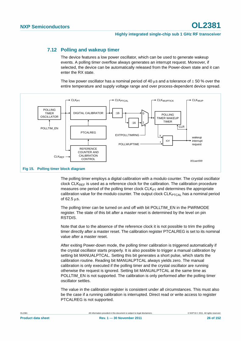
7.12 Polling and wakeup timer
The device features a low power oscillator, which can be used to generate wakeup events. A polling timer overflow always generates an interrupt request. Moreover, if selected, the device can be automatically released from the Power-down state and it can enter the RX state.
The low power oscillator has a nominal period of 40 s and a tolerance of 50 % over the entire temperature and supply voltage range and over process-dependent device spread.
The polling timer employs a digital calibration with a modulo counter. The crystal oscillator clock CLKREF is used as a reference clock for the calibration. The calibration procedure measures one period of the polling timer clock CLKPT and determines the appropriate calibration value for the modulo counter. The output clock CLKPTCAL has a nominal period of 62.5 s.
The polling timer can be turned on and off with bit POLLTIM_EN in the PWRMODE register. The state of this bit after a master reset is determined by the level on pin RSTDIS.
Note that due to the absence of the reference clock it is not possible to trim the polling timer directly after a master reset. The calibration register PTCALREG is set to its nominal value after a master reset.
After exiting Power-down mode, the polling timer calibration is triggered automatically if the crystal oscillator starts properly. It is also possible to trigger a manual calibration by setting bit MANUALPTCAL. Setting this bit generates a short pulse, which starts the calibration routine. Reading bit MANUALPTCAL always yields zero. The manual calibration is only executed if the polling timer and the crystal oscillator are running otherwise the request is ignored. Setting bit MANUALPTCAL at the same time as POLLTIM_EN is not supported. The calibration is only performed after the polling timer oscillator settles.
The value in the calibration register is consistent under all circumstances. This must also be the case if a running calibration is interrupted. Direct read or write access to register PTCALREG is not supported.
Fig 15. Polling timer block diagram
001aan599
POLLINGTIMER
OSCILLATORPOLLING
TIMER WAKEUPTIMER
wakeupinterruptrequest
DIGITAL CALIBRATOR :16 0
1
x
CLR
r x≥r
:16
EXTPOLLTIMRNG
POLLWUPTIME
PTCALREG
REFERENCECOUNTER ANDCALIBRATION
CONTROL
POLLTIM_EN
CLKPT CLKPTCAL CLKWUPTICK CLKWUP
CLKREF
OL2381 All information provided in this document is subject to legal disclaimers. © NXP B.V. 2011. All rights reserved.
Product data sheet Rev. 1 — 30 November 2011 26 of 152

NXP Semiconductors OL2381Highly integrated single-chip sub 1 GHz RF transceiver
The polling timer wakeup time can be set with the 8-bit control register POLLWUPTIME. The wakeup time calculates to:
(2)
The achievable resolution and wakeup times can be selected in two different ranges, a normal and an extended polling timer range according to the setting of bit EXTPOLLTIMRNG in the CLOCKCON register.
It is possible to change the register POLLWUPTIME while the polling timer is running. If the new value is greater than the polling timer counter’s current content, the running period is not interrupted and the newly set wakeup time is seamlessly adjusted. This mechanism allows the setting of a new wakeup time with respect to the last wakeup event. If the newly set value in register POLLWUPTIME is smaller than the polling timer counter’s current content, the counter is reset immediately.
The digital calibration is implemented so that the accuracy of wakeup times greater than 10 ms is better than 1 %. This allows an overall timing error of less than 2 % for the given range.
7.12.1 Actions at polling timer wakeup
Register POLLACTION defines which action the device carries out after a polling timer event; see Section 8.2.1.14 “Polling action register POLLACTION” on page 102.
POLL_MODE[1:0] defines the device’s operating mode after a polling timer event.
RX_GAIN[1:0] means the same as the RX flags RE and RF (gain step/switch selection bits). The RX_CMD bit means the same as RX flag RC. It allows a choice between a WUPS (0) and a PRDA command (1). RX_FREQ[1:0] means the same as RX flags RA and RB (frequency selection).
The last bit in the POLLACTION register, SET_RX_FLAGS, defines whether the RX flag register’s current content is used for the automatically initiated RX command (if 0) or whether the RX flags RA, RB, RC, RE and RF flags are overwritten with the contents of the RX_FREQ, RX_CMD and RX_GAIN bit settings of this register, respectively, before the command is actually launched (if 1). If the flags are overwritten, RX flag RD is set to logic 1 to make the sub-command either a WUPS or a PRDA command; see Section 7.32.2 “Receive command” on page 55 for more information.
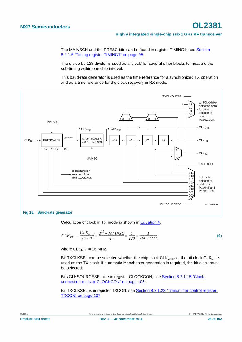
7.13 RX and TX baud-rate generator
The baud-rate generator generates the nominal, unsynchronized chip clock according to Equation 3.
(3)
where PRESC is an exponent in the range from 0 to 7, and 211 + MAINSC is the mantissa in the range 2048 to 4095. The resulting baud-rate clock can jitter by one prescaler clock cycle CLKPSC.
The mainscaler MAINSCL lower bits can be found in register TIMING0.
TWUP POLLWUPTIME 1+ TWUPTICK=
b aud rate16 MHz
2PRESC
------------------ 211
MAINSC+
212
------------------------------------- 1128---------=
OL2381 All information provided in this document is subject to legal disclaimers. © NXP B.V. 2011. All rights reserved.
Product data sheet Rev. 1 — 30 November 2011 27 of 152
NXP Semiconductors OL2381Highly integrated single-chip sub 1 GHz RF transceiver
The MAINSCH and the PRESC bits can be found in register TIMING1; see Section 8.2.1.5 “Timing register TIMING1” on page 95.
The divide-by-128 divider is used as a ‘clock’ for several other blocks to measure the sub-timing within one chip interval.
This baud-rate generator is used as the time reference for a synchronized TX operation and as a time reference for the clock-recovery in RX mode.
Calculation of clock in TX mode is shown in Equation 4.
(4)
where CLKREF = 16 MHz.
Bit TXCLKSEL can be selected whether the chip clock CLKCHIP or the bit clock CLKBIT is used as the TX clock. If automatic Manchester generation is required, the bit clock must be selected.
Bits CLKSOURCESEL are in register CLOCKCON; see Section 8.2.1.15 “Clock connection register CLOCKCON” on page 103.
Bit TXCLKSEL is in register TXCON; see Section 8.2.1.23 “Transmitter control register TXCON” on page 107.
Fig 16. Baud-rate generator
001aan600
PRESCALER MAIN SCALER× 0.5 ... × 0.999
MAINSC
0 1
CLKPSC CLKMSC
to test functionselector of portpin P12/CLOCK
÷2 ÷4 ÷8 ÷16
÷2presc
PRESC
CLKREF ÷32 ÷2 ÷2 ÷2
0 1
0
1
111to SCLK driverselection or tofunctionselector ofport pinP12/CLOCK
CLKCHIP
CLKBIT
CLKTX
TXCLKSEL
TXCLKOUTSEL
CLKSOURCESEL
000110
111
to functionselector ofport pinsP11/INT andP12/CLOCK
100011010001000
101110
CLKTX
CLKREF
2PRESC
--------------------- 211
MAINSC+
212
------------------------------------- 1128--------- 1
2TXCLKSEL
--------------------------=
OL2381 All information provided in this document is subject to legal disclaimers. © NXP B.V. 2011. All rights reserved.
Product data sheet Rev. 1 — 30 November 2011 28 of 152

NXP Semiconductors OL2381Highly integrated single-chip sub 1 GHz RF transceiver
7.13.1 Clock recovery for RX mode
The clock-recovery for RX mode is dependent on the baud rate accuracy. If the absolute correct baud rate cannot be selected, choose the next available integer value. The clock recovery is able to cope with a 1 % tolerance to be able to operate correctly with standard XTAL cutting and temperature inaccuracies. The clock recovery is implemented as a digital phase control loop with a fixed operating frequency determined by the baud-rate generator setting. The baud-rate generator’s mainscaler clock acts as the reference clock for the clock-recovery PLL (128 times the actual chip clock). The clock recovery PLL is programmable with regards to its settling speed. The settling of the clock-recovery speed can be set to reach its final state within 3, 7, 15 or 31 chips. If the clock-recovery is locked to the bit-stream the actual possible phase-error is proportional to the selected settling speed setting. Highest settling speed (settling within 3 chips) produces the smallest actual phase error due to fast regulation; slowest speed (settling within 31 chips), allows for the largest phase error due to the slowest regulation time constant; see Table 103 “CLOCK_RECOV_TC bit functions” on page 118.
Note that the decoding of NRZ signals with long constant bit-periods is directly influenced by the accuracy of the selected baud rate. Proper coding can significantly improve sensitivity and the BER of NRZ decoding.
7.14 Phase-locked loop
A complete on-chip PLL is available to provide an RF carrier in both RX and TX modes. The PLL is a 4th-order fractional-N PLL. The PLL analog section is described in Section 7.14.1 and the PLL digital section is described in Section 7.14.7.
7.14.1 PLL building blocks
All PLL building blocks except bit VCO_BAND in register LOCON and the charge pump reference current (PLL_ICP[4:0]) settings are automatically configured and operated by selecting the corresponding device modes. The following paragraphs describe the function of the internal control signals. These control signals can be influenced, if desired, by operating control bits located in the EXPERTn and TESTn registers.
7.14.2 PLL and VCO regulators
To operate the whole PLL, both regulators must be switched on; see Section 7.9.3 “PLL regulator” on page 19.
Fig 17. PLL block diagram
001aan601MAIN DIVIDER
1.2 GHz to1.856 GHz
VCO
UP loop filter
DOWN
PFD
chargepump
16 MHzreference
signal
OL2381 All information provided in this document is subject to legal disclaimers. © NXP B.V. 2011. All rights reserved.
Product data sheet Rev. 1 — 30 November 2011 29 of 152
NXP Semiconductors OL2381Highly integrated single-chip sub 1 GHz RF transceiver
7.14.3 General PLL operation
The following blocks are enabled after switching on the regulators so that the entire PLL is operational: VCO (VCO_ON), phase-detector (PFD_ON), prescaler (PRESC_ON) and reference clock buffer (CLK_PLL_ON), depending on the selected mode of operation (RX or TX mode, selected via device mode or command); eventually RX_ON must be also set. If this bit is set to logic 1, the RX LO dividers are activated.
7.14.4 Charge pump
This block delivers the charge to the loop filter. The polarity and amount of charge are proportional to the phase error reported by the phase detector.
The peak current of this charge pump is automatically adjusted. It can be overridden by PLL_ICP[4:0] in register EXPERT0; see Section 8.2.4.1 “Register EXPERT0” on page 124. The charge pump peak current is a function of the icp control bits: icp[0] * 15 A + icp[1] * 30 A + icp[2] * 60 A + icp[3] * 120 A + icp[4] * 240 A.
This means that a value from 15 A up to 465 A can be selected. The purpose of this programmability is to compensate for gain variation in other blocks, especially RF VCO, and to keep a constant PLL loop bandwidth. The recommend value is to set PLL_ICP to 2.
7.14.5 RF VCO
The very low phase-noise on-chip RF oscillator is based on an LC oscillator.
A capacitor bank is integrated to center the resonant frequency of the LC tank on the desired RF frequency. The VCO auto-calibration routine automatically trims the VCO to the correct sub-band. Whenever a different frequency setting is used for TX or RX operation, the VCO auto-calibration is carried out automatically. Automatic trimming can be blocked by setting bit SKIP_VCO_CAL in the LOCON register except during the PLL start-up; see Section 8.2.1.3 “Local oscillator control register LOCON” on page 95. The trimming (sub-band selection) can be manually modified by control bits VCO_SUBBAND[5:0] in register VCOCON; see Section 8.2.1.2 “VCO control register VCOCON” on page 94. Frequency sub-band setting 0 corresponds to the maximum frequency, and 3Fh to the minimum frequency.
Note that this RF VCO is running at twice (868 MHz and 928 MHz bands) or four times (313 MHz and 434 MHz bands) the chosen frequency bands.
Setting bit VCO_BAND selects the VCO’s appropriate operating mode. This bit must be set to logic 1 at RF frequency bands below 400 MHz, or set to logic 0 for all other bands.
7.14.6 PLL loop bandwidth setting
It is recommended that the PLL loop bandwidth is set to just above 150 kHz (3 dB closed loop bandwidth) as this gives the best trade off between noise behavior and locking time. The loop bandwidth can be set by PLL_ICP[4:0] to the recommended value ICP = 2.
7.14.7 Delta-sigma modulator for fractional-N synthesis
The operating frequency is set by the content of frequency control registers FC0 to FC3, which each have a width of 20 bits. The ‘active’ frequency control register is selected directly by the TX or RX command; see Section 8.2.1.1 “Frequency control registers” on page 93.
OL2381 All information provided in this document is subject to legal disclaimers. © NXP B.V. 2011. All rights reserved.
Product data sheet Rev. 1 — 30 November 2011 30 of 152
xxxxxxxxxxxxxxxxxxxxx xxxxxxxxxxxxxxxxxxxxxxxxxx xxxxxxx x x x xxxxxxxxxxxxxxxxxxxxxxxxxxxxxx xxxxxxxxxxxxxxxxxxx xx xx xxxxx xxxxxxxxxxxxxxxxxxxxxxxxxxx xxxxxxxxxxxxxxxxxxx xxxxxx xxxxxxxxxxxxxxxxxxxxxxxxxxxxxxxxxxx xxxxxxxxxxxx x x xxxxxxxxxxxxxxxxxxxxx xxxxxxxxxxxxxxxxxxxxxxxxxxxxxx xxxxx xxxxxxxxxxxxxxxxxxxxxxxxxxxxxxxxxxxxxxxxxxxxxxxxxx xxxxxxxx xxxxxxxxxxxxxxxxxxxxxxxxx xxxxxxxxxxxxxxxxxxxx xxx
OL2
381
Pro
du
ct data sh
NX
P S
emico
nd
ucto
rsO
L2381
Hig
hly
integ
rate
d sin
gle-ch
ip su
b 1
GH
z RF
tran
sc
eiver
vant control word (Pt) for the PLL. d are therefore converted into a lta modulator. It produces numbers in
f the sequence generated by the y occur in the RF spectrum. To ant 1-bit to the given fractional part, low. It creates a tiny frequency offset Cx for a given center frequency.
001aan602
15 16last A, B
LSB= 1
RF_LO_DIV
DOUBLE_SD_RESULT
P(t)
MASH 1 to 1ΣΔ
S(t)
-1 to 2
-2 to 4
S6
0
×2
DISFRAC
S30
15
All inform
ation provided in this docum
ent is subject to legal disclaim
ers.©
NX
P B
.V. 20
11. All rights reserved
.
eetR
ev. 1 — 30 N
ovem
ber 2011
31 of 15
2
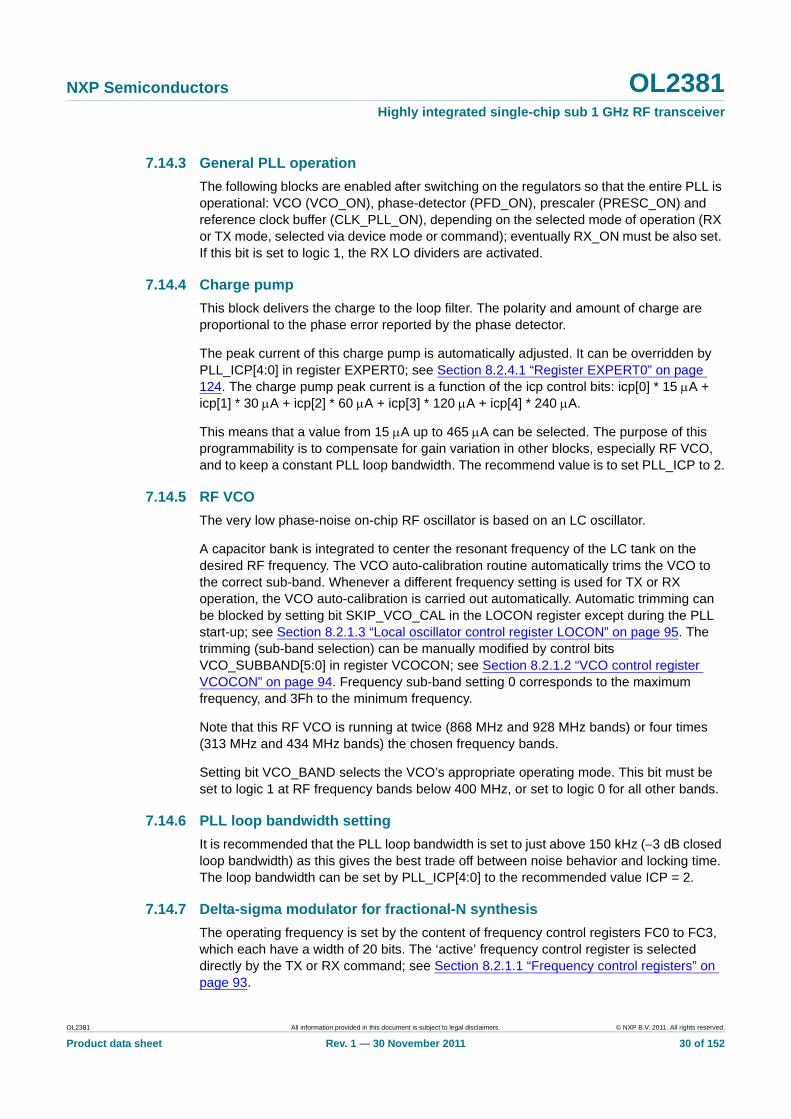
7.14.7.1 PLL operating frequency f0
In Figure 18, the integer (Nt) is forwarded directly to the adder which produces the releThe remaining fractional values cannot be handled by the frequency divider directly anpseudo-random sequence of integers. This conversion is implemented by the sigma dethe range from 1 to +2, whose average over time equals the given fractional part.
The spectral purity of the resulting RF signal is highly dependent on the randomness ofractional part. If this contained short repetitive patterns unwanted spurious signals maguarantee the produced sequences are always of maximal length, we append a constwhich resolves the issue. The weight of this 16th bit is 1 / 216 = 1 / 65536, which is verywhich can be taken into account when calculating the center frequency control value F
Fig 18. Computing the frequency divider control word
20
S12
S4
S5
20FC0
S1 C F(t)
5
N(t)
S11
M(t)2
K(t)
D(t)
flags
FC1
FC2
FC3
1228
FDEV_MANT
FDEV_EXP
RX TX and FSK enable
0
1NEG
LSBs
MSBs
MANT × 2exp
SLEW-RATECONTROL
DIVIDER
DIVIDER
FRMP_EXP
FRMP_MANT
MODULATOR
modulationsignal
0
1
5
3
U11
O
S11
-D
≠0
S2
1
10
D S11
S11
3
4
NXP Semiconductors OL2381Highly integrated single-chip sub 1 GHz RF transceiver
When the fractional part approaches 0 or 1 the low frequency noise components in the pseudo-random sequence become more dominant and can no longer be sufficiently suppressed by the PLL’s transfer function. The visible effect is an increase of the phase noise in the RF output near the carrier. To counteract this effect, the OL2381 uses bit DOUBLE_SD_RESULT (Double Sigma Delta Result). If this bit is set, the fractional contribution to the PLL control word is doubled. So when the frequency control value F(t) is increased linearly, each RF output frequency is produced twice; once with a fractional value that is closer to zero or one (between 0 and 1 / 4 or between 3 / 4 and 1) and a second time with a fractional value which is closer to the mid-value 1 / 2 (between 1 / 4 and 3 / 4). The latter value produces a good pseudo-random sequence.
The frequency control value’s fractional part is processed differently depending on bit DOUBLE_SD_RESULT, and the center frequency changes accordingly. Therefore the formulae, which convert between a given Frequency Control (FC) value and the RF center frequency, change with the state of bit DOUBLE_SD_RESULT.
In normal mode the expression is straightforward as shown in Equation 5.
(5)
• The expression’s left side shows the reference frequency. The output frequency varies proportionally with the reference.
• The parenthesized expression (64 + 2 …) is the characteristics of the PLL frequency divider.
• The right term in the parenthesized expression accounts for the number interpretation of C and F(t) and the constant 1 LSB, which is added to guarantee maximum length sequences from the sigma-delta modulator
• The fraction at the right is the output division ratio, which is either 1 / 2 or 1 / 4, depending on the setting of bit RF_LO_DIV.
After simplifying the expression further we get the results shown in Equation 6.
(6)
For the inverse we solve the above expression for FCx and then we round the result to the nearest integer number as shown in Equation 7.
(7)
Using the floor function this becomes as shown in Equation 8.
(8)
Remark: Equation 8 is an important equation.
fRF fref 64 22 FCx 1+
65536-----------------------------+
12 2 RF_LO_DIV+--------------------------------------------------=
fRF fref 322 FCx 1+
65536-----------------------------+
11 RF_LO_DIV+-----------------------------------------=
FCx roundfRF
fref------- 1 RF_LO_DIV+ 32–
32768 0.5–
=
FCxfRF
fref------- 1 RF_LO_DIV+ 32–
32768=
OL2381 All information provided in this document is subject to legal disclaimers. © NXP B.V. 2011. All rights reserved.
Product data sheet Rev. 1 — 30 November 2011 32 of 152
NXP Semiconductors OL2381Highly integrated single-chip sub 1 GHz RF transceiver
If bit DOUBLE_SD_RESULT is set, the integer part and the fractional part of the center frequency setting must be considered separately. In this case the expression for the output frequency is shown in Equation 9.
(9)
In the inner parenthesized expression the integer part is taken as is, where the term which contains the fractional part has an additional factor of 2. After canceling certain factors of 2 we get result shown in Equation 10.
(10)
The inverse of this function is problematic, because the function for the output frequency is not monotonous. But we know that each output frequency is produced exactly twice and we know also that we want the solution where the average of the sigma-delta output S(t) is closest to 1 / 2. Let us convert Equation 10 such that the integer part of the frequency control value has no factor and the term containing the fractional part of the frequency control value becomes isolated on one side of the equation as shown in Equation 11.
(11)
Now we ask for the integer part for which the fractional part becomes a value in the range from 0.25 to 0.75, which is equivalent to twice the fractional part, and lies between 0.5 and 1.5 as shown in Equation 12 and Equation 13.
(12)
(13)
Now we can isolate the integer part from both inequalities so that the right sides are the same as shown in Equation 14 and Equation 15.
(14)
(15)
These inequalities can be combined into a single expression to calculate the integer control value for the PLL as shown in Equation 16.
(16)
Remark: Equation 16 is an important equation.
fRF fref 64 2 FCx 19:15 22 FCx 14:0 1+
65536---------------------------------------------+
+ 1
2 2 RF_LO_DIV+--------------------------------------------------=
fRF fref 32 FCx 19:15 2 FCx 14:0 1+32768
---------------------------------------------+ + 1
1 RF_LO_DIV+-----------------------------------------=
fRF
fref------- 1 RF_LO_DIV+ 32 FCx 19:15 –– 2 FCx 14:0 1+
32768--------------------------------------------- 2 fract= =
fRF
fref------- 1 RF_LO_DIV+ 32 FCx 19:15 0.5––
fRF
fref------- 1 RF_LO_DIV+ 32 FCx 19:15 1.5––
FCx 19:15 fRF
fref------- 1 RF_LO_DIV+ 32 0.5––
FCx 19:15 +1fRF
fref------- 1 RF_LO_DIV+ 32 0.5––
FCx 19:15 fRF
fref------- 1 RF_LO_DIV+ 32.5–=
OL2381 All information provided in this document is subject to legal disclaimers. © NXP B.V. 2011. All rights reserved.
Product data sheet Rev. 1 — 30 November 2011 33 of 152
NXP Semiconductors OL2381Highly integrated single-chip sub 1 GHz RF transceiver
The integer part which we have just found can be entered in Equation 10 and then we can solve for the fractional part. We get the result for the settings after rounding it to the nearest integer number shown in Equation 17.
(17)
When using the floor function this becomes as shown in Equation 18.
(18)
Remark: Equation 18 is an important equation.
From Equation 5 and Equation 10 we can also see which frequency resolution can be achieved in which mode. If bit DOUBLE_SD_RESULT is set to logic 0, we have Equation 19.
(19)
If bit DOUBLE_SD_RESULT is set to logic 1, the resolution becomes as shown in Equation 20.
(20)
Taking bit DOUBLE_SD_RESULT into the formula, Equation 19 and Equation 20 can be combined into
(21)
Remark: Equation 21 is an important equation.
7.14.8 RX frequency offset
Because the OL2381 receiver implements a superheterodyne architecture with an intermediate frequency of 300 kHz, the local oscillator is automatically tuned to300 kHz above the wanted RX center frequency in RX mode. ThisRX frequency offset is independent of the RF_LO_DIVand DOUBLE_SD_RESULT settings.
This is accomplished by adding an offset value O to the center frequency setting C; see Figure 18 “Computing the frequency divider control word” on page 31. This offset value is automatically adjusted so that it matches the LO frequency resolution, which changes with the settings of bits RF_LO_DIV and DOUBLE_SD_RESULT.
Table 70 “RX frequency offset” on page 107 shows that the resulting RX frequency offset is independent of the RF_LO_DIV and DOUBLE_SD_RESULT settings. It is always 195 Hz below the nominal IF of 300 kHz, which is accurate enough in all cases.
FCx 14:0 roundfRF
fref------- 1 RF_LO_DIV+ 32 FCx 19:15 ––
16384 0.5–
=
FCx 14:0 fRF
fref------- 1 RF_LO_DIV+ 32 FCx 19:15 ––
16384=
fRF res 0 fref 2 265536--------------- 1
2 2 RF_LO_DIV+--------------------------------------------------
fref
32768--------------- 1
1 RF_LO_DIV+-----------------------------------------==
fRF res 1 fref 2 265536--------------- 1
2 2 RF_LO_DIV+--------------------------------------------------
fref
16384--------------- 1
1 RF_LO_DIV+-----------------------------------------==
fRF resfref
32768--------------- 1 DOUBLE_SD_RESULT+
1 RF_LO_DIV+----------------------------------------------------------------------=
OL2381 All information provided in this document is subject to legal disclaimers. © NXP B.V. 2011. All rights reserved.
Product data sheet Rev. 1 — 30 November 2011 34 of 152
NXP Semiconductors OL2381Highly integrated single-chip sub 1 GHz RF transceiver
7.14.9 PLL lock detection
A lock detection circuit is implemented to support the shortest PLL power-on time. The lock-detection circuit monitors the phase and frequency differences of the PLL and the reference clock. If the phase-difference of the two clock signals is settled within a defined window, an internal LOCK_DETECT signal is triggered. After a specified time, set by bit LOCK_DET_TIME[1:0] in register EXPERT1, status bit LO_RDY is set in register DEVSTATUS. Since the lock detect circuit consumes additional power, it is only enabled during the PLL’s start-up phase and whenever a different sub-band setting is applied. The lock detect circuit can be manually controlled by bit LOCK_DET_ON in register LOCON; see Section 8.2.1.3 “Local oscillator control register LOCON” on page 95.
7.15 VCO auto-calibration
VCO calibration is performed every time the VCO’s center frequency is changed. The following internal sequences are started:
1. Start VCO calibration and turn on PLL lock detection. The output of the lock detection must be gated LOW when the calibration is running.
2. With the next clock cycle: turn on phase frequency detector (bit PFD_ON), prescaler (bit PRESC_ON), clock for PLL (bit CLK_PLL_ON) and PLL lock detection.
3. Perform VCO calibration (select best possible sub-band for desired frequency setting).
4. Check PLL lock detection plus lock detect time.
7.16 TX operation
7.16.1 TX mode
7.16.1.1 Preparation for TX mode
TX mode is initiated by setting the device mode bits DEV_MODE[1:0] to 11b or by sending a TX command. The necessary VCO, PLL and PA start-up is accomplished by the internal state machine. Completion of the start-up sequence is indicated by bit TX_RDY in the special function register DEVSTATUS.
7.16.2 TX command
The power amplifier is activated on the first active edge of the TX command’s ninth bit. Therefore, the active edge for the power amplifier start-up differs from the active edge of the remaining SPI communication. This must be considered for the data set-up time of the transmitted bit.
Predefined configurations can be chosen for the TX sequence. The configuration bits are described in Table 4.
Table 4. TX command bits
TA TB TC TD TE TF
TX frequency selection bits data and power amplifier synchronization bit
power amplifier control bit
Manchester generation bit
amplitude selection bit
OL2381 All information provided in this document is subject to legal disclaimers. © NXP B.V. 2011. All rights reserved.
Product data sheet Rev. 1 — 30 November 2011 35 of 152

NXP Semiconductors OL2381Highly integrated single-chip sub 1 GHz RF transceiver
[1] If bit TE = 1, the value of bit TC is ignored and data is always synchronized with the baud-rate clock. However, bit TC has an effect if bit TD = 1. Therefore, bit TC must be properly set even if TE = 1.
Table 5. TX command packet
D0 D1 D2 D3 D4 D5 D6 D7
1 1 TA TB TC TD TE TF
Table 6. Control of TX data (bits TC, TE)[1]
TC TE Effect
0 0 TX data is unsynchronized (only synchronized to CLKREF)
1 0 TX data is synchronized with the baud-rate clock (CLKTX)
X 1 TX data is synchronized and XORed with the baud-rate clock (CLKTX), hence Manchester generation is applied
Table 7. Power amplifier control and synchronization (bits TC, TD)
TC TD Effect
X 0 power amplifier stays on after falling edge of SEN
0 1 power amplifier turns off on the falling edge of SEN (PA off-ramping supported)
1 1 power amplifier turns off synchronously with the baud-rate clock (CLKTX) after the falling edge of SEN (PA off-ramping supported)
Table 8. Summary of combined TC, TD and TE bits
TC TD TE Function
0 0 0 unsynchronized TX data and PA stays on
0 0 1 Manchester coded data and PA stays on
0 1 0 unsynchronized TX data and falling edge of SEN turns off PA
0 1 1 Manchester coded data and falling edge of SEN turns off PA
1 0 0 synchronized TX data and PA stays on.
1 0 1 Manchester coded data and PA stays on
1 1 0 Synchronized TX data and PA turns off synchronously (CLKTX) after the falling edge of SEN
1 1 1 Manchester coded data and PA turns off synchronously (CLKTX) after the falling edge of SEN
Table 9. Amplitude selection (bit TF)
Bit TF Effect
0 modulation and amplitude/power settings are applied according to register ACON0
1 modulation and amplitude/power settings are applied according to register ACON1
OL2381 All information provided in this document is subject to legal disclaimers. © NXP B.V. 2011. All rights reserved.
Product data sheet Rev. 1 — 30 November 2011 36 of 152

NXP Semiconductors OL2381Highly integrated single-chip sub 1 GHz RF transceiver
Table 10. Frequency band selection (bits TA, TB)
Bit TA Bit TB Selected frequency band
0 0 FC0L, FC0M, FC0H
0 1 FC1L, FC1M, FC1H
1 0 FC2L, FC2M, FC2H
1 1 FC3L, FC3M, FC3H
TA to TF contain configuration information for TX operation.
Fig 19. TX data timing diagram (SEP_TX_LINES = 0)
SEN
reset baud-rate generator andturn on power amplifier
power amplifier switched offor data sent continouslySCLK
externaldriver
SCLK
SCLKinternal
driver
SDIOinternal
driver
SDIO
001aan603
1 TA TB TC TD TE TF
command and flagsTA and TB
evaluated here
flags TC to TFevaluated here
TX DATA TX DATA TX DATA1
SDIOexternal
driver1 TA TB TC TD TE TF TX DATA TX DATA TX DATA1
OL2381 All information provided in this document is subject to legal disclaimers. © NXP B.V. 2011. All rights reserved.
Product data sheet Rev. 1 — 30 November 2011 37 of 152
NXP Semiconductors OL2381Highly integrated single-chip sub 1 GHz RF transceiver
7.16.3 Example of synchronized data transmission
TA to TF contain configuration information for TX operation.
Fig 20. TX data timing diagram (SEP_TX_LINES = 1)
SEN
reset baud-rate generator andturn on power amplifier
SCLKexternal
driver
SCLK
SCLKinternal
driver
P12/CLOCKinternal
driver001aan604
SDIO 1 TA TB TC TD TE TF1
P10/DATAexternal
driver
SDIOexternal
driver1 TA TB TC TD TE TF1
SDIOinternal
driver
TX DATA TX DATA TX DATA
Table 11. Phase 1: data transmission
D0 D1 D2 D3 D4 D5 D6 D7
1 1 0 0 1 0 1 0
- - selection of frequency configuration register FC0
synchronization of TX data with positive edge of TX clock CLKTX
PA stays on after falling edge of SEN, TX data is stored and continuously sent
Manchester code generation is selected
Modulation and amplitude/power settings of ACON0 are applied
Table 12. Phase 2: end data transmission
D0 D1 D2 D3 D4 D5 D6 D7
1 1 0 0 1 1 1 0
- - selection of frequency configuration register FC0
synchronization of TX data with positive edge of TX clock CLKTX
PA turned off in synchronization with TX clock CLKTX after falling edge of SEN
Manchester code generation is selected
Modulation and amplitude/power settings of ACON0 are applied
OL2381 All information provided in this document is subject to legal disclaimers. © NXP B.V. 2011. All rights reserved.
Product data sheet Rev. 1 — 30 November 2011 38 of 152

xxxxxxxxxxxxxxxxxxxxx xxxxxxxxxxxxxxxxxxxxxxxxxx xxxxxxx x x x xxxxxxxxxxxxxxxxxxxxxxxxxxxxxx xxxxxxxxxxxxxxxxxxx xx xx xxxxx xxxxxxxxxxxxxxxxxxxxxxxxxxx xxxxxxxxxxxxxxxxxxx xxxxxx xxxxxxxxxxxxxxxxxxxxxxxxxxxxxxxxxxx xxxxxxxxxxxx x x xxxxxxxxxxxxxxxxxxxxx xxxxxxxxxxxxxxxxxxxxxxxxxxxxxx xxxxx xxxxxxxxxxxxxxxxxxxxxxxxxxxxxxxxxxxxxxxxxxxxxxxxxx xxxxxxxx xxxxxxxxxxxxxxxxxxxxxxxxx xxxxxxxxxxxxxxxxxxxx xxx
OL2
381
Pro
du
ct data sh
NX
P S
emico
nd
ucto
rsO
L2381
Hig
hly
integ
rate
d sin
gle-ch
ip su
b 1
GH
z RF
tran
sc
eiver
the special function bits the actual TX clock CLKTX.
Section 8.2.1.23 “Transmitter control
001aan605
power amplifier switched on
''0'' ''1'' ''0'' ''1'' ''0'' ''1'' ''0'' ''1'' ''0'' ''1' ''1'' ''0'' ''1'' ''0'' ''1'' ''0'' ''1'' ''0'' ''1'' ''1''''0'' ''0''
Manchester coded data
power amplifierswitched off synchronizedwith CLKTX after fallingedge of SEN
automatic Manchester new TX data
TXDATA
TX DATA
N
data stored afterfalling edge of SEN
K
All inform
ation provided in this docum
ent is subject to legal disclaim
ers.©
NX
P B
.V. 20
11. All rights reserved
.
eetR
ev. 1 — 30 N
ovem
ber 2011
39 of 15
2
7.16.4 Clock output selection for the TX command
The clock output at port pins SCLK or P12/CLOCK respectively, can be selected with TXCLKOUTSEL[1:0]. With this mechanism it is possible to provide a faster clock than
If no clock is selected, TXCLKOUTSEL = 11b and the device behaves as follows; seeregister TXCON” on page 107:
• SEP_TX_LINES = 0: the output driver of SCLK is never activated
Fig 21. TX data example
PHASE 1: DATA TRANSMISSION
CLKTX reset
code generationsynchronized with CLKTX'
synchronizedwith CLKTX'
CLKTX
SCLK
SDIO 1 1 0 0 1 10 0 TX DATA
SEN
data storedafter falling edgeof SEN
power amplifier switched on
SEN
SCLK
SDIO
1 1 0 0 1 11 0
PHASE 2: END OF DATA TRANSMISSIO
SCLK
SDIO
SEN
data at SDIO accepted as TXdata after ninth edge of SCL

NXP Semiconductors OL2381Highly integrated single-chip sub 1 GHz RF transceiver
• SEP_TX_LINES = 1: the line P12/CLOCK drives a constant HIGH level; see Section 8.2.1.9 “Port control register PORTCON2” on page 99
7.17 Power amplifier
The power amplifier is driven from the PLL synthesizer and operates in single-ended mode.
The power amplifier consists of six binary-weighted output stages which are connected in parallel and are operated according to the amplifier control register settings ACON0, ACON1 and ACON2; see Section 8.2.1.19 “Register ACON0” on page 105. Though the PA’s supply voltage is configurable to 3 different voltage settings, it is advised to use only the PAM 0 setting for the majority of applications.
The device features several control bits controlling the output amplitude and ASK modulation characteristics of the power amplifier. The control registers ACON0 to ACON2 control the power amplifier stage for either amplitude fine tuning or ASK modulation. Bit ASK0 located in register ACON0 and bit ASK1 located in register ACON1 determine ASK or FSK operation.
The lower 5 bits of control registers ACON0, ACON1 and ACON2 allow the setting of two different high levels (AMH0 and AMH1) and one low level (AML) respectively, which define the modulation depth during amplitude modulation of the UHF carrier. Which two available AMHx registers is used is selected by TX command flag bit TF. Amplitude modulation is achieved by switching between the selected high and low levels in accordance with the internal signal AMOUT, which is derived from the TX data stream.
Fig 22. Power amplifier control
001aan606
AMPLITUDERAMP
CONTROL
flag TF
AMH0
AMH1
AML
modulation data
ASK0
ASK1
ARMP
poweramplifiercontrol
0
1
amout
acon
0
1
0
1
OL2381 All information provided in this document is subject to legal disclaimers. © NXP B.V. 2011. All rights reserved.
Product data sheet Rev. 1 — 30 November 2011 40 of 152
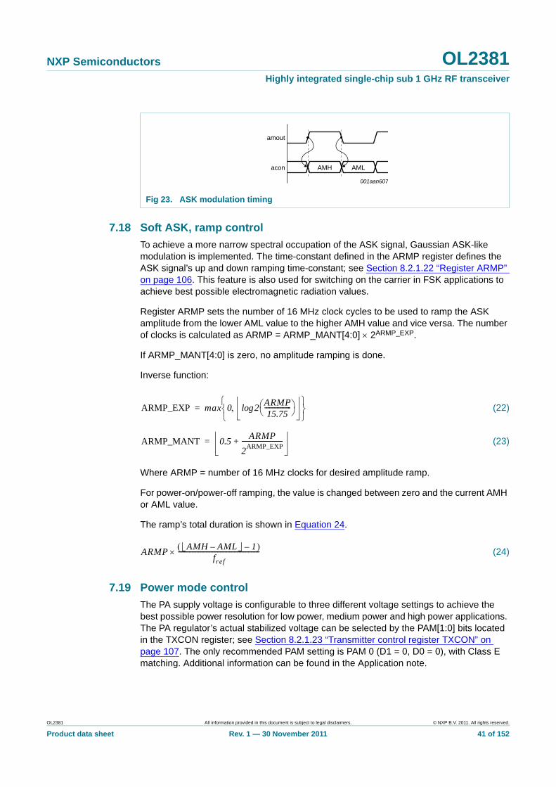
NXP Semiconductors OL2381Highly integrated single-chip sub 1 GHz RF transceiver
7.18 Soft ASK, ramp control
To achieve a more narrow spectral occupation of the ASK signal, Gaussian ASK-like modulation is implemented. The time-constant defined in the ARMP register defines the ASK signal’s up and down ramping time-constant; see Section 8.2.1.22 “Register ARMP” on page 106. This feature is also used for switching on the carrier in FSK applications to achieve best possible electromagnetic radiation values.
Register ARMP sets the number of 16 MHz clock cycles to be used to ramp the ASK amplitude from the lower AML value to the higher AMH value and vice versa. The number of clocks is calculated as ARMP = ARMP_MANT[4:0] 2ARMP_EXP.
If ARMP_MANT[4:0] is zero, no amplitude ramping is done.
Inverse function:
(22)
(23)
Where ARMP = number of 16 MHz clocks for desired amplitude ramp.
For power-on/power-off ramping, the value is changed between zero and the current AMH or AML value.
The ramp’s total duration is shown in Equation 24.
(24)
7.19 Power mode control
The PA supply voltage is configurable to three different voltage settings to achieve the best possible power resolution for low power, medium power and high power applications. The PA regulator’s actual stabilized voltage can be selected by the PAM[1:0] bits located in the TXCON register; see Section 8.2.1.23 “Transmitter control register TXCON” on page 107. The only recommended PAM setting is PAM 0 (D1 = 0, D0 = 0), with Class E matching. Additional information can be found in the Application note.
Fig 23. ASK modulation timing
001aan607
amout
AMHacon AML
ARMP_EXP max 0 2ARMP15.75
----------------- log
=
ARMP_MANT 0.5ARMP
2ARMP_EXP
--------------------------+=
ARMPAMH AML– 1–
fref----------------------------------------------------
OL2381 All information provided in this document is subject to legal disclaimers. © NXP B.V. 2011. All rights reserved.
Product data sheet Rev. 1 — 30 November 2011 41 of 152
NXP Semiconductors OL2381Highly integrated single-chip sub 1 GHz RF transceiver
7.20 PLL frequency deviation (FSK)
7.20.1 Frequency modulation
FSK and GFSK-type modulation is accomplished by adding a time-varying sequence to the center frequency control value. This variation in the total frequency control value is slow enough to pass the PLL’s transfer function and the resulting RF is modulated in frequency; see Section 7.14.3 “General PLL operation” on page 30 for a detailed description of operation.
The FSK path starts by computing the frequency deviation value D from the given FDEV_EXP[2:0] and FDEV_MANT[4:0] values; see Equation 25.
(25)
The RF_LO_DIV and DOUBLE_SD_RESULT bits are included in this expression to compensate for the influence of these bits on the frequency resolution. If the argument of the floor function is an integer, which is the case for all but 72 of the 1024 possible setting combinations, then the result of the floor function equals its argument. In these cases the resulting frequency deviation is independent from the RF_LO_DIV and DOUBLE_SD_RESULT bits.
(26)
Note that in Equation 26, DSR and RLD are bits DOUBLE_SD_RESULT and RF_LO_DIV respectively. After canceling out the dependency from these bits we get the following simple result.
(27)
If the argument of the floor function is not an integer, the result is multiplied with the current frequency resolution, which is equivalent to rounding the result from Equation 27 down to the next available frequency step.
Frequency deviation is calculated as shown in Equation 28 and Equation 29.
(28)
(29)
Where:
FDEV = 65536 fdev / fref
fdev = desired frequency deviation
fref = reference frequency (16 MHz)
D 2FDEV_EXP
FDEV_MANT12--- 1 RF_LO_DIV+
1 DOUBLE_SD_RESULT+----------------------------------------------------------------------=
fdev 2FDEV_EXP
FDEV_MANT12--- 1 RLD+
1 DSR+---------------------
fref
32768--------------- 1 DSR+
1 RLD+---------------------=
fdev2
FDEV_EXPFDEV_MANT
65536-------------------------------------------------------------------- fref=
FDEV_MANT min 31 0.5 + FDEV
2FDEV_EXP
-------------------------
=
FDEV_EXP min 7, max 1 DOUBLE_SD_RESULT+1 RF_LO_DIV+
---------------------------------------------------------------------- 2FDEV15.75---------------- log,
=
OL2381 All information provided in this document is subject to legal disclaimers. © NXP B.V. 2011. All rights reserved.
Product data sheet Rev. 1 — 30 November 2011 42 of 152
NXP Semiconductors OL2381Highly integrated single-chip sub 1 GHz RF transceiver
The modulation signal controls the RF output such that a logic 0 produces +D (the high frequency, fRF = fcenter + fdev) and logic 1 selects D (the low frequency, fRF = fcenter fdev). If FRMP_MANT is logic 0, the resulting squarewave shaped sequence is the modulating sequence M(t).
7.20.2 Soft FSK
A GFSK-type modulation scheme is implemented to achieve a narrower signal bandwidth of the FSK spectrum. The GFSK shape is modeled by a linear interpolation approach. The FSK frequency shifting is done linearly between FRF FDEV and FRF + FDEV. The linear ramp is implemented by stepping the frequency control value between +D and D at a step rate (sr), using a step increment (si). Both variables are controlled by FRMP_EXP[2:0] and FRMP_MANT[3:0] according to the expressions in Equation 30 and Equation 31.
(30)
(31)
When FRMP_EXP[2:0] = 4, the scaling factor for the step rate is 1 and so is the step increment si. When FRMP_EXP[2:0] is greater than 4, the step rate is decreased in powers of two and the step increment is kept at 1. Likewise, when FRMP_EXP[2:0] is less than 4, the step increment is increased in powers of two and the step rate scaling factor is kept at 1. These two dependencies taken together result in a continuous scaling of the ramp’s slew rate.
When we multiply these two expressions together, we get the ramp’s slew rate in steps per second shown in Equation 32.
(32)
(33)
To find what the soft FSK ramp’s slew rate is in terms of Hz/s, we have to multiply the expression in Equation 33 with the frequency resolution shown in Equation 34 and Equation 35.
(34)
(35)
If we want to get the FRMP settings from a given slew rate, we need the inverse function.
(36)
Soft FSK parameters are calculated as shown below:
srfref
2min(0,FRMP_EXP-4)
FRMP_MANT--------------------------------------------------------------------------------------= increment/s
si 2min(0,4-FRMP_EXP)
= steps
slew rate fref2
min(0,4-FRMP_EXP)
2min(0,FRMP_EXP-4)
FRMP_MANT--------------------------------------------------------------------------------------= steps/s
slew rate fref2
min(0,4-FRMP_EXT)-min(0,FRMP_EXP-4)
FRMP_MANT------------------------------------------------------------------------------------= steps/s
slew rate fref2
4-FRMP_EXT
FRMP_MANT------------------------------------
fref
32768--------------- 1 DOUBLE_SD_RESULT+
1 RF_LO_DIV+----------------------------------------------------------------------=
slew ratefref 2
2048 FRMP_MANT 2FRMP_EXP
--------------------------------------------------------------------------------------- 1 DOUBLE_SD_RESULT+1 RF_LO_DIV+
----------------------------------------------------------------------=
FRMP_MANT 2FRMP_EXP
fref 2
2048 slew rate--------------------------------------- 1 DOUBLE_SD_RESULT+
1 RF_LO_DIV+----------------------------------------------------------------------=
OL2381 All information provided in this document is subject to legal disclaimers. © NXP B.V. 2011. All rights reserved.
Product data sheet Rev. 1 — 30 November 2011 43 of 152

NXP Semiconductors OL2381Highly integrated single-chip sub 1 GHz RF transceiver
Given:
fref = reference frequency (crystal frequency: 16 MHz).
fdev = frequency deviation.
RampTime = wanted time for ramping, to reduce occupied bandwidth.
Search:
FRMP_EXP and FRMP_MANT, in order to program register FRMP.
Calculation:
1. Calculate the frequency resolution: .
DOUBLE_SD_RESULT and RF_LO_DIV can be logic 0 or logic 1 and are described elsewhere in this datasheet.
2. Calculate the frequency steps; see Figure 24: .
3. Calculate the slew rate: .
4. Calculate the FRMP_EXP and FRMP_MANT:
7.21 Oscillator and divider settings
Different oscillator divider and PLL divider settings can be selected to enable operation at all ISM bands. The configuration information is located in the LOCON register; see Section 8.2.1.3 “Local oscillator control register LOCON” on page 95.
Bit RF_LO_DIV controls the local oscillator’s output frequency divider. If this bit is logic 0, the divider divides the VCO frequency by 2 so that the LO produces RF frequencies above 500 MHz; if the bit is logic 1, the divider divides by 4 producing frequencies below 500 MHz.
Fig 24. Soft FSK parameters
001aao143
Steps
Ramp Time
+fdev
fdev
fRF resfref
32768--------------- 1 DOUBLE_SD_RESULT+
1 RF_LO_DIV+----------------------------------------------------------------------=
Steps2 fdevfRF,res
------------------=
Slew rateSteps
RampTime----------------------------=
FRMP_EXP min 7, max 0 2fref 16
SlewRate 7.75---------------------------------------log
=
FRMP_MANT min 15 0.5fref 16
SlewRate 2FRMP_EXP
-------------------------------------------------------+
=
OL2381 All information provided in this document is subject to legal disclaimers. © NXP B.V. 2011. All rights reserved.
Product data sheet Rev. 1 — 30 November 2011 44 of 152

NXP Semiconductors OL2381Highly integrated single-chip sub 1 GHz RF transceiver
7.22 Modulation data generation
Depending on the setting of bit SEP_TX_LINES in register PORTCON2, either pin SDIO or pin P10/DATA act as the data input; see Section 8.2.1.9 “Port control register PORTCON2” on page 99. Input data is synchronized to the reference clock CLKREF. This flip-flop serves also as storage for the input data. Input data is sampled under the following conditions.
• Bit SEP_TX_LINES = logic 0: input data sampling starts with the ninth bit of the TX command and stops when the command ends, hence SEN goes LOW. The last input state is stored.
• Bit SEP_TX_LINES = logic 1: input data sampling starts with the ninth bit of the TX command which turns on the power amplifier and stops when the power amplifier is turned off again. Intermediate SPI read, write or TX commands which do not alter the power amplifier’s state do not influence data sampling.
The sampled input data is either provided transparently, synchronized to the baud rate or Manchester coded, depending on the current TX flags TC and TE. Baud-rate synchronization and Manchester code generation runs with the TX clock CLKTX. Data is updated with every positive clock edge of CLKTX and, if Manchester coding is selected, it is inverted with the negative clock edge of CLKTX.
The data stream can be optionally inverted by setting bit INV_TX_DATA. This inversion is located after the storage elements. If the stored data is constant, it is possible to alter modulation data by an SPI write access to bit INV_TX_DATA; see Section 8.2.1.23 “Transmitter control register TXCON” on page 107.
7.23 TX operating mode
7.23.1 Power-down
In this mode the device consumes little current and the registers do not change. All transmitter, receiver, clock generator, and amplifier blocks are switched off.
When the power-down state is left (by the rising edge of SEN) the PD bit is cleared.
7.23.2 Idle mode
In this mode the device is powered up. The crystal oscillator or the external clock buffer is enabled and after crystal oscillator stabilization (if selected) the device is supplied with the reference clock.
7.23.3 Active mode
Active mode is entered when the device mode bits are set to anything other than logic 00. The digital regulator and XTAL are always activated. If active mode logic 01 is chosen, the VCO and the PLL are also started. If SPI state is entered, communication between a microcontroller and the registers is enabled via the SPI interface. The active state can beleft by programming a register indicating another state or by setting SEN LOW for more than 4 ms.
OL2381 All information provided in this document is subject to legal disclaimers. © NXP B.V. 2011. All rights reserved.
Product data sheet Rev. 1 — 30 November 2011 45 of 152
NXP Semiconductors OL2381Highly integrated single-chip sub 1 GHz RF transceiver
7.23.3.1 PLL active TX mode
The TX mode is entered on reception of a valid TX command, providing the PLL is settled. Depending on the TX command’s content, TX mode exits either directly when SEN is set LOW, or when synchronized with the last data bit’s edge when SEN is set LOW or directly on the SPI register setting. The power amplifier is turned on at the ninth bit’s first active edge of the TX command. Therefore, the active edge for the power amplifier start-up differs from the active edge of the remaining SPI communication. This must be considered for the data set-up time of the transmitted bit. Any SPI clock following the ninth bit is ignored by the SPI interface. If during a TX sequence a POR or power fail condition occurs, the XTAL active mode is entered. More information can be found in Section 7.16.2 “TX command” on page 35.
7.23.4 Baud-rate generation
The baud rate for the TX data is generated by the baud-rate generator. This baud-rate generator is used for TX and RX operation at the same time; see Section 7.13 “RX and TX baud-rate generator” on page 27 for a detailed explanation.
7.23.5 TX mode clock selection
Depending on the setting of bit TXCLKSEL in register TXCON, different clock sources can be selected; see Section 8.2.1.23 “Transmitter control register TXCON” on page 107. TXCLKSEL = logic 1selects the baud-rate generator’s bit clock. TXCLKSEL = logic 0 selects the chip clock. If Manchester modulation is required, the bit clock is selected. Bit INV_TX_DATA in register TXCON is used to invert the TX data stream.
7.24 RX operation
Figure 25 visualizes internal signal shapes inside the RX block. Signal 1 represents the signal input spectrum, sketched in the frequency domain. The frequency spectrum is centered to the desired RX frequency. Signal 2 represents the amplified spectrum of the input signal (signal 1). Signal 2 is mixed with the LO frequency (must be set to 300 kHz above the RX frequency) down from the RX input frequency with the I and the Q mixer to the IF (300 kHz). Signal 3 and signal 6 represent the IF signals of the I and the Q channel (90 phase difference) in the time domain. Signals 4 and 7 represent the I and Q signals after the channel filter. Signals 5 and 8 are the amplified and limited I and Q signals at the output of the limiter. It is possible to switch some of these internal analog signals to pins
Fig 25. RX signal diagram
4 5
7 8
85
t
A
1 2
3
6
74
t
A
1A
2A
3 6
t
A
f
f
001aan608
LNA
RSSI
limiter
limiter
CHANNELFILTER
OL2381 All information provided in this document is subject to legal disclaimers. © NXP B.V. 2011. All rights reserved.
Product data sheet Rev. 1 — 30 November 2011 46 of 152
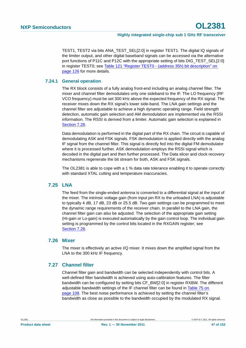
NXP Semiconductors OL2381Highly integrated single-chip sub 1 GHz RF transceiver
TEST1, TEST2 via bits ANA_TEST_SEL[2:0] in register TEST1. The digital IQ signals of the limiter output, and other digital baseband signals can be accessed via the alternative port functions of P11C and P12C with the appropriate setting of bits DIG_TEST_SEL[2:0] in register TEST0; see Table 121 “Register TEST0 - (address 35h) bit description” on page 126 for more details.
7.24.1 General operation
The RX block consists of a fully analog front-end including an analog channel filter. The mixer and channel filter demodulates only one sideband to the IF. The LO frequency (RF VCO frequency) must be set 300 kHz above the expected frequency of the RX signal. The receiver mixes down the RX signal’s lower side-band. The LNA gain settings and the channel filter are adjustable to achieve a high dynamic operating range. Field strength detection, automatic gain selection and AM demodulation are implemented via the RSSI information. The RSSI is derived from a limiter. Automatic gain selection is explained in Section 7.28.
Data demodulation is performed in the digital part of the RX chain. The circuit is capable of demodulating ASK and FSK signals. FSK demodulation is applied directly with the analog IF signal from the channel filter. This signal is directly fed into the digital FM demodulator where it is processed further. ASK demodulation employs the RSSI signal which is decoded in the digital part and then further processed. The Data slicer and clock recovery mechanisms regenerate the bit stream for both, ASK and FSK signals.
The OL2381 is able to cope with a 1 % data rate tolerance enabling it to operate correctly with standard XTAL cutting and temperature inaccuracies.
7.25 LNA
The feed from the single-ended antenna is converted to a differential signal at the input of the mixer. The intrinsic voltage gain (from input pin RX to the unloaded LNA) is adjustable to typically 4 dB, 17 dB, 23 dB or 25.5 dB. Two gain settings can be programmed to meet the dynamic range requirements of the receiver chain. In parallel to the LNA gain, the channel filter gain can also be adjusted. The selection of the appropriate gain setting (Hi-gain or Lo-gain) is executed automatically by the gain control loop. The individual gain setting is programmed by the control bits located in the RXGAIN register; see Section 7.28.
7.26 Mixer
The mixer is effectively an active I/Q mixer. It mixes down the amplified signal from the LNA to the 300 kHz IF frequency.
7.27 Channel filter
Channel filter gain and bandwidth can be selected independently with control bits. A well-defined filter bandwidth is achieved using auto-calibration features. The filter bandwidth can be configured by setting bits CF_BW[2:0] in register RXBW. The different adjustable bandwidth settings of the IF channel filter can be found in Table 75 on page 108. The best noise performance is achieved by setting the channel filter’s bandwidth as close as possible to the bandwidth occupied by the modulated RX signal.
OL2381 All information provided in this document is subject to legal disclaimers. © NXP B.V. 2011. All rights reserved.
Product data sheet Rev. 1 — 30 November 2011 47 of 152
NXP Semiconductors OL2381Highly integrated single-chip sub 1 GHz RF transceiver
7.27.1 Channel filter auto-calibration
The channel filter auto-calibration is implemented to achieve a well-centered filter roll-off characteristic in the filter pass-band. This feature can compensate for process and temperature dependent parameter mismatches. Filter auto-calibration is performed automatically before every RX operation.
The calibration can be blocked by setting bit SKIP_CF_RC_CAL, and can be forced at any time by setting bit FORCE_CF_RC_CAL both in register TEST4.
Channel filter calibration status information can be accessed by reading the CFRCCAL register. All CFRCCAL register bits are read-only.
After starting channel filter calibration, bit CF_RC_CAL_RUNNING in register CFRCCAL can be probed. This bit is set to logic 1 when the RC calibration algorithm is running.
CF_RC_CAL_RES[3:0] indicate the channel RC calibration result. These bits are applied directly to the internal RC components of the channel filter.
Channel filter auto-calibration can be manually overridden by special register TEST4. Control bits CF_RC_ADJUSTCAL[1:0] allow the accuracy of the channel filter auto-calibration routine to be cross-checked.
Setting bit SKIP_CF_RC_CAL by-passes the on-chip RC-calibration. Setting bit FORCE_CF_RC_CAL triggers an RC auto-calibration. The corresponding RC calibration values set in CF_RC_CAL_RES[3:0] in register CFRCCAL after auto-calibration, have to be entered in MAN_CF_RC_CALVAL[3:0] in register TEST4.
The CF_RC_ADJUSTCAL[1:0] control bits can be used to evaluate the on-chip channel filter RC calibration block accuracy. The R part of the RC reference is trimmed by changing the value of these two bits. By knowing the adjusted R variation we can verify that the output of the CF_RC_CAL_RES[3:0] control bits is changing accordingly. This enables the complete RC measurement mechanism to be validated.
7.27.2 Channel I/Q calibration
An I/Q calibration is implemented to achieve a high image frequency rejection. This calibration is intended to be used once during production of the final application PCB as part of an end-of-line test. It requires an external signal at the image frequency of the desired RX frequency to be applied to pin RX. The I/Q calibration routine automatically calculates the best I/Q trimming configuration for the optimum image rejection of >50 dBc. This result must be read and stored by the external microcontroller. The calibration value is valid for the whole frequency band over all supply voltages and temperatures.
Perform the I/Q calibration as follows:
Apply a signal at the RX image frequency. The signal level must be chosen so that the RSSI is still able to measure the damped image; for example, an input of 40 dBm gives an image at 90 dBm, which is still a sufficient RSSI operating margin.
The I/Q calibration is enabled by setting bit START_CF_IQ_CAL in register CFIQCAL. Status bit CF_IQ_CAL_RUNNING indicates an active calibration cycle. All possible I/Q offset combinations are run sequentially at every combination an RSSI measurement is performed. The combination with the minimum RSSI reading is stored in
OL2381 All information provided in this document is subject to legal disclaimers. © NXP B.V. 2011. All rights reserved.
Product data sheet Rev. 1 — 30 November 2011 48 of 152
NXP Semiconductors OL2381Highly integrated single-chip sub 1 GHz RF transceiver
CF_IQ_CALVAL[6:0]. This information must be stored by the external microcontroller. Initialize this register with the stored values each time. Set CF_IQ_CALVAL[6:0] to logic 0 if no IQ calibration is required.
Figure 26 shows the effect of a simulated I/Q calibration. With this calibration an image rejection of 50 dB is achievable.
7.28 LNA and channel filter gain settings
Table 13 gives the intrinsic voltage gain of the LNA circuit. LNA voltage gain is programmable and this table indicates the incremental ICC steps impacting RX front-end current consumption.
CF-BW = Channel filter bandwidth.
Fig 26. Simulation examples for I/Q calibration with different channel filter bandwidth settings
IMAGE CHANNEL
21.5 dB@ 300 kHz
case 2200 kHz CF-BW
−24 dB to −29 dB(I/Q calibration)@ −300 kHz
−500
−60
−70
−50
−40
−30
−20
−10
0
10
20
30
−100 300 700f (kHz)
IMAGE CHANNEL
22.7 dB@ 300 kHz
case 150 kHz CF-BW
−25 dB to −65 dB(I/Q calibration)@ −300 kHz
−500 −130
−110
−90
−70
−50
−30
−10
10
30
−100 300 700f (kHz)
(dB) (dB)
001aan609
Table 13. Channel filter gain settings
Channel filter gain 1 Channel filter gain 0 Voltage gain (dB)
0 0 2
0 1 17
1 0 22
1 1 27
Table 14. RX gain control
LNA gain 1 LNA gain 0 Gain (dB) LNA input stage typical current (mA)
0 0 4[1] 0.55
OL2381 All information provided in this document is subject to legal disclaimers. © NXP B.V. 2011. All rights reserved.
Product data sheet Rev. 1 — 30 November 2011 49 of 152

NXP Semiconductors OL2381Highly integrated single-chip sub 1 GHz RF transceiver
[1] LNA low gain stage.
Voltage gain induced by an impedance transformation network (from antenna to input pin RX) needs to be added to the values in Table 13 (such as 6 dB extra gain in case of ideal 50 to 200 impedance transformation) to compute the overall RX front-end voltage gain.
The RX analog chain voltage gain (before limiter) can be performed by adding these values to those of the channel filter given in Table 13.
Figure 27 and Figure 28 show the field-strength as a function of gain switching.
0 1 17 0.55
1 0 23 1.1
1 1 25.5 1.65
Fig 27. 20 dB difference between Hi-gain and Lo-gain setting
Table 14. RX gain control …continued
LNA gain 1 LNA gain 0 Gain (dB) LNA input stage typical current (mA)
001aan610
switch
RSSI
+30 %
1.3
1
Pin (dBm)−120 −100 −70 −40
OL2381 All information provided in this document is subject to legal disclaimers. © NXP B.V. 2011. All rights reserved.
Product data sheet Rev. 1 — 30 November 2011 50 of 152
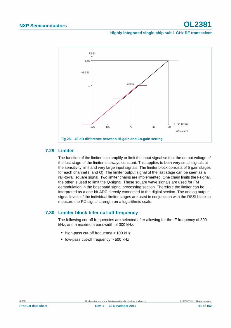
NXP Semiconductors OL2381Highly integrated single-chip sub 1 GHz RF transceiver
7.29 Limiter
The function of the limiter is to amplify or limit the input signal so that the output voltage of the last stage of the limiter is always constant. This applies to both very small signals at the sensitivity limit and very large input signals. The limiter block consists of 5 gain stages for each channel (I and Q). The limiter output signal of the last stage can be seen as a rail-to-rail square signal. Two limiter chains are implemented. One chain limits the I-signal, the other is used to limit the Q-signal. These square wave signals are used for FM demodulation in the baseband signal processing section. Therefore the limiter can be interpreted as a one-bit ADC directly connected to the digital section. The analog output signal levels of the individual limiter stages are used in conjunction with the RSSI block to measure the RX signal strength on a logarithmic scale.
7.30 Limiter block filter cut-off frequency
The following cut-off frequencies are selected after allowing for the IF frequency of 300 kHz, and a maximum bandwidth of 300 kHz:
• high-pass cut-off frequency < 100 kHz
• low-pass cut-off frequency > 500 kHz
Fig 28. 40 dB difference between Hi-gain and Lo-gain setting
001aan611
switch
RSSI
+65 %
1.65
1
Pin (dBm)−120 −100 −70 −40 −20
OL2381 All information provided in this document is subject to legal disclaimers. © NXP B.V. 2011. All rights reserved.
Product data sheet Rev. 1 — 30 November 2011 51 of 152
NXP Semiconductors OL2381Highly integrated single-chip sub 1 GHz RF transceiver
7.31 RSSI
The RSSI function is implemented by adding tail currents used in the individual limiter stages. This does not apply to levels higher than the compression point. In thiscase the gain of the LNA and channel filter is reduced to increase the linearity and the dynamic range of the RSSI.
Remark: As the RSSI is proportional to the input voltage level having a frequency of 300 kHz, it must be filtered to ensure a stable result as the input voltage. The RSSI frequency is 600 kHz due to the nature of the RSSI detector principle.
7.31.1 Dynamic range and operation
The RSSI’s dynamic operation is required for ASK demodulation and carrier detection. An overall dynamic range of 130 dB is required, 120 dBm minimum sensitivity up to +10 dBm maximum signal strength. The front-end gain can be switched. An overlap of the dynamic ranges of 20 dB is recommended to guarantee continuous ASK demodulation. This results in a single range of 70 dB. The RSSI value can be used to reduce the power output of a TX operation. The RSSI value can be included in the handshaking information with appropriate TX power settings applied.
7.31.2 Resolution
The resolution is set to 2 dB in all conditions. A 6-bit converter is implemented to allow for process and temperature variations.
Fig 29. Signal level plan
DIGITALFM
DEMODULATOR
RSSI
limiter
channelfilter
reference-60 dBm
LNA
conversion gain =30 dB, 35 dB, 25 dBor 5 dB
sensitivity =-116 dBm
IF = 300 kHz IF = 300 kHzpin = -71 dBm to 5 dBm
IF = 300 kHzsignal level = -12 dBVp(diff)
(= 250 mVpdiff, 10 Vt)
gain = 25 dB, 0 dB, 10dBor 35 dB
gain = -12 + 81 = 69 dBmin14 dB per stage (nominal)
gain control
bufferI
Q
001aan612
mixer
OL2381 All information provided in this document is subject to legal disclaimers. © NXP B.V. 2011. All rights reserved.
Product data sheet Rev. 1 — 30 November 2011 52 of 152

NXP Semiconductors OL2381Highly integrated single-chip sub 1 GHz RF transceiver
7.31.2.1 RSSI low-pass filtering
The filter integration time-constant of the analog RSSI signal can be adapted to achieve a more stable digital RSSI reading (RSSI raw value) as an input to the digital filtering and interpolation. The RC-type analog filter is used in addition to the digital filters implemented in the baseband digital signal processing unit. This first order low-pass filter is applied directly to the summed output of the limiter tail-currents. The limiter gain bandwidth characteristics are not affected.
7.31.2.2 RSSI digital filtering
The raw RSSI value is fed to a digital filtering and interpolation circuit. The output of the digital circuit is the digitized RSSI value. The digital RSSI filter cut-off frequency can be selected by bits RSSI_FILTER_FC[3:0] in register RXBW.
The first-order low-pass filter previously mentioned cut-off frequency can be calculated according to the Equation 37.
(37)
Where fref is the reference frequency and RSSI_FILTER_FC[3:0] is a 4 bit value in register RXBW; see Section 8.2.1.25 “Channel filter bandwidth and RSSI filter settings register RXBW” on page 108.
7.31.2.3 Low-level signal detection
The RSSI is used to detect the start of a communication sequence. Carriers at a sensitivity level as low as 110 dBm are detected properly.
7.31.3 RSSI gain control
The automatic front-end gain selection switching threshold is controlled by the RSSI’s output signal. This principle decreases the gain of the front-end and, if necessary, the channel filter when the input level is significantly greater than the reference sensitivity level. This gain switching increases the linearity of the overall chain and the robustness for large signal behavior and also increases the RSSI’s dynamic range.
Register HIGAINLIM contains control word HI_GAIN_LIMIT[7:0]; see Section 8.2.1.27 “Register HIGAINLIM” on page 109. At power-up the front-end gain is always set to the value of RX_HI_GAIN[4:0] in register RXGAIN, so that the RSSI operates in its most sensitive mode; see Section 8.2.1.24 “Receiver gain control register RXGAIN” on page
Fig 30. Block diagram of RSSI
STATEMACHINE
start clk
001aan613
IRSSI
32lo
limiter
16lo8lo4lo2lolo
fcfref
2 25+RSSI_FILTER_FC
-------------------------------------------------------=
OL2381 All information provided in this document is subject to legal disclaimers. © NXP B.V. 2011. All rights reserved.
Product data sheet Rev. 1 — 30 November 2011 53 of 152
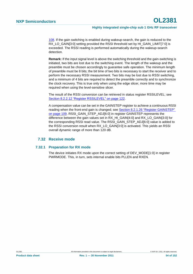
NXP Semiconductors OL2381Highly integrated single-chip sub 1 GHz RF transceiver
108. If the gain switching is enabled during wakeup-search, the gain is reduced to the RX_LO_GAIN[3:0] setting provided the RSSI threshold set by HI_GAIN_LIMIT[7:0] is exceeded. The RSSI reading is performed automatically during the wakeup-search detection.
Remark: If the input signal level is above the switching threshold and the gain-switching is initiated, two bits are lost due to the switching event. The length of the wakeup and the preamble must be chosen accordingly to guarantee safe operation. The minimum length of preamble must be 8 bits; the bit time of two bits is necessary to start the receiver and to perform the necessary RSSI measurement. Two bits may be lost due to RSSI switching, and a minimum of 4 bits are required to detect the preamble correctly and to synchronize the clock recovery. This is true only when using the edge slicer, more time may be required when using the level-sensitive slicer.
The result of the RSSI conversion can be retrieved in status register RSSILEVEL; see Section 8.2.2.12 “Register RSSILEVEL” on page 122.
A compensation value can be set in the GAINSTEP register to achieve a continuous RSSI reading when the front-end gain is changed; see Section 8.2.1.26 “Register GAINSTEP” on page 109. RSSI_GAIN_STEP_ADJ[6:0] in register GAINSTEP represents the difference between the gain values set in RX_HI_GAIN[4:0] and RX_LO_GAIN[3:0] for the corresponding RSSI read value. The RSSI_GAIN_STEP_ADJ[6:0] value is added to the RSSI conversion result when RX_LO_GAIN[3:0] is activated. This yields an RSSI overall dynamic range of more than 120 dB.
7.32 Receive mode
7.32.1 Preparation for RX mode
The device initiates RX mode upon the correct setting of DEV_MODE[1:0] in register PWRMODE. This, in turn, sets internal enable bits PLLEN and RXEN.
OL2381 All information provided in this document is subject to legal disclaimers. © NXP B.V. 2011. All rights reserved.
Product data sheet Rev. 1 — 30 November 2011 54 of 152
NXP Semiconductors OL2381Highly integrated single-chip sub 1 GHz RF transceiver
1. Turn on the bandgap reference circuit for the receiver section (bit RX_GAP_ON) and the clock for the channel filter RC calibration (CLK_RXA_ON) with the negative edge of the reference clock. The latter is done only if the channel filter RC calibration is not skipped (bit SKIP_CF_RC_CAL). Then wait 1 μs until the bandgap stabilizes.
2. If the channel filter RC calibration is enabled, start it and then wait until it ends. Then turn off the clock for the RC calibration at the next falling edge of the reference clock.
3. Wait until the PLL control-state machine reaches the state PLL_LOCKED and then turn the receiver on (bit RX_ON), which also turns on the VCO clock divider in the receiver section.
This sequence ends with the channel filter RC calibration, if enabled. When this ends, the receiver is turned on.
7.32.2 Receive command
The device features a RX command comparable to the TX command. The command includes the six command bits RA, RB, RC, RD, RE and RF:
• RA, RB: RX frequency selection bits
• RC, RD: sub-command bits
• RE, RF: gain step/switch selection bits
Fig 31. Preparation for RX mode
001aan614
ENTER RECEIVEMODE
RX_GAP_ON = 1
SKIP_CF_RC_CAL CLK_RXA_ON = 1
FALLING EDGE OFREF CLK TURNS
CALIBRATION CLK OFF
CF_RC_CAL_OK0
0
1
1
RX_ON = 1VCO CLOCK DIVIDERFOR RECEIVER PART
ON
1
WAIT 1 μs
PLL_LOCKED
Table 15. Receive command packet
D0 D1 D2 D3 D4 D5 D6 D7
1 0 RA RB RC RD RE RF
OL2381 All information provided in this document is subject to legal disclaimers. © NXP B.V. 2011. All rights reserved.
Product data sheet Rev. 1 — 30 November 2011 55 of 152
NXP Semiconductors OL2381Highly integrated single-chip sub 1 GHz RF transceiver
Remark: In RX mode a frequency offset of +300 kHz is automatically added to the resulting center frequency to account for the necessary LO frequency offset. If this is the first RX command after a TX operation or whenever these flags change from one RX command to another, an LO sub-band calibration (VCO calibration) is initiated.
With a CONT RX command, the microcontroller can continue with any previously initiated WUPS, DATA or PRDA command. If the frequency selection bits RA and RB are the same as in the previous RX command and if the flags RE and RF are both logic 0, then, with the next rising edge of SCLK, only the RX clock and the RX data lines are switched to the SPI SCLK and D(I)O pins, respectively. This provides the microcontroller with the possibility to interlace SPI Read and Write commands with RX data, provided that the SPI communication rate is much faster than the data reception rate. If no RX operation is in progress, no initiation occurs, and the CONT RX command only switches the SPI lines with the next SPI clock edge, and delivers the internal RX result. The RX result can be the recovered chip clock and the transparent slicer signal or just a constant level, depending on the current RX output configuration and depending on the RX state.
A WUPS RX command initiates a wakeup search operation. This command’s restart characteristics enable it to interrupt any RX operation. During this command the RXDCON0 configuration is applied as the dynamic configuration for the slicer and signal classification and detection; the RX clock and data result can be observed with the SPI lines producing a constant HIGH on the clock line and a constant LOW on the data line in digitized mode. This output (not the wakeup search operation itself) can be interrupted with Read and Write commands and can be continued with a CONT RX command. The WUPS command ends after either a WAKEUP_FOUND or a WAKEUP_NOT_FOUND decision. In both cases the status of the detection method is sampled. When the WUPS command ends, the WUPS_FOLLOWUP configuration dictates how the device operates; see Table 20 “RX operating mode transitions” on page 61.
A PRDA RX command initiates a preamble detection. This command’s restart characteristics enable it to interrupt any other RX operation. During this command the RXDCON1 configuration is applied as the dynamic configuration for the slicer and signal classification and detection method; the RX clock and data result can be observed with the SPI lines producing a constant HIGH on the clock line and a constant HIGH on the data line during preamble detection in digitized mode. This output (not the preamble
Table 16. Frequency selection (bits RA, RB)
Bit RA Bit RB Selected frequency band
0 0 FC0L, FC0M, FC0H
0 1 FC1L, FC1M, FC1H
1 0 FC2L, FC2M, FC2H
1 1 FC3L, FC3M, FC3H
Table 17. Sub-command selection bits RC, RD
Bit RC Bit RD Selected RX sub-command
0 0 CONT (continue)
0 1 WUPS (wakeup search)
1 0 PRDA (preamble detection followed by data
reception)
1 1 DATA (data reception without preamble
detection)
OL2381 All information provided in this document is subject to legal disclaimers. © NXP B.V. 2011. All rights reserved.
Product data sheet Rev. 1 — 30 November 2011 56 of 152
NXP Semiconductors OL2381Highly integrated single-chip sub 1 GHz RF transceiver
detection operation itself) can be interrupted with Read and Write commands and can be continued with a CONT RX command. When the correct preamble is detected, the receiver switches automatically into data reception mode. This switch does not influence the signal processing section of the receiver, which means that there is a seamless transition from the preamble detection mode to the data reception mode. What changes with the switch is the dynamic part of the configuration and the state of the signal detection and classification means. The dynamic configuration for the signal detection and classification method is switched to the RXDCON2 set and the detection methods are restarted.
If the preamble detection ends with a PREAMBLE_NOT_FOUND status (after running into a timeout), the PREA_FOLLOWUP configuration automatically decides if and how the receiver operates; see Table 20 “RX operating mode transitions” on page 61. Regardless of the outcome of the preamble detection phase (found or timeout) the status of the detection method is sampled when the preamble detection ends.
If the digitized RX output format is selected for the RX clock and data, both are held constant while the preamble detection is in progress. When the preamble is detected, the RX clock starts and the associated RX data bits are delivered with each RX clock pulse. In transparent mode the output signals are always available.
A DATA RX command initiates the reception of frame data and skipping the preamble detection phase. This command always uses the RXDCON2 set as the dynamic configuration for the slicer and the signal detection and classification methods. After initializing the slicer it behaves similar to the PRDA command after successful preamble detection.
Both the PRDA command in data reception mode and the DATA command do not end automatically on any selectable criteria. They can be terminated with either a TX command or another restarting RX command, or by turning the receiver off.
The combination logic 01 (gain switch) is only applicable with the wakeup search (WUPS) RX command. If this is chosen, the wakeup search starts with the high gain settings. If the received RF signal strength is always below the limit given by the HI_GAIN_LIMIT settings, then the low gain settings are used throughout the whole wakeup search. But if the RF amplitude exceeds this limit, the receiver automatically switches to the low gain settings and continues with the wakeup search. Note that the wakeup search timer is not influenced by the gain switch.
Table 18. Gain switch selection (bits RE, RF)
Bit RE Bit RF Selected gain step/switch configuration
0 0 keep RX gain as is
0 1 gain switch (WUPS sub-command only), same as logic 00 for other sub-commands
1 0 use low gain settings
1 1 use high gain settings
OL2381 All information provided in this document is subject to legal disclaimers. © NXP B.V. 2011. All rights reserved.
Product data sheet Rev. 1 — 30 November 2011 57 of 152
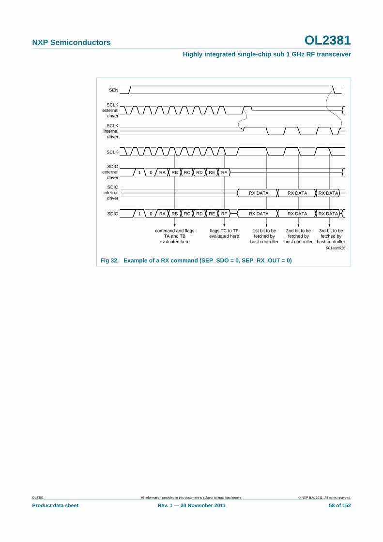
NXP Semiconductors OL2381Highly integrated single-chip sub 1 GHz RF transceiver
Fig 32. Example of a RX command (SEP_SDO = 0, SEP_RX_OUT = 0)
SEN
SCLKexternal
driver
SCLK
SCLKinternal
driver
SDIOinternal
driver
SDIO
001aan615
1 RA RB RC RD RE RF
command and flagsTA and TB
evaluated here
flags TC to TFevaluated here
RX DATA RX DATA RX DATA0
1 0SDIO
externaldriver
RA RB RC RD RE RF
RX DATA RX DATA RX DATA
1st bit to befetched by
host controller
2nd bit to befetched by
host controller
3rd bit to befetched by
host controller
OL2381 All information provided in this document is subject to legal disclaimers. © NXP B.V. 2011. All rights reserved.
Product data sheet Rev. 1 — 30 November 2011 58 of 152
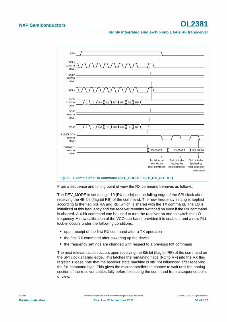
NXP Semiconductors OL2381Highly integrated single-chip sub 1 GHz RF transceiver
From a sequence and timing point of view the RX command behaves as follows:
The DEV_MODE is set to logic 10 (RX mode) on the falling edge of the SPI clock after receiving the 4th bit (flag bit RB) of the command. The new frequency setting is applied according to the flag bits RA and RB, which is shared with the TX command. The LO is initialized at this frequency and the receiver remains switched on even if the RX command is aborted. A 4-bit command can be used to turn the receiver on and to switch the LO frequency. A new calibration of the VCO sub-band, provided it is enabled, and a new PLL lock-in occurs under the following conditions.
• upon receipt of the first RX command after a TX operation
• the first RX command after powering up the device
• the frequency settings are changed with respect to a previous RX command
The next relevant action occurs upon receiving the 8th bit (flag bit RF) of the command on the SPI clock’s falling edge. This latches the remaining flags (RC to RF) into the RX flag register. Please note that the receiver state machine is still not influenced after receiving the full command byte. This gives the microcontroller the chance to wait until the analog section of the receiver settles fully before executing the command from a sequence point of view.
Fig 33. Example of a RX command (SEP_SDO = 0, SEP_RX_OUT = 1)
SEN
SCLKexternal
driver
SCLK
SCLKinternal
driver
P12/CLOCKinternal
driver
P10/DATAinternal
driver
001aan616
RX DATA RX DATA RX DATA
1 0SDIO
externaldriver
RA RB RC RD RE RF
1st bit to befetched by
host controller
2nd bit to befetched by
host controller
3rd bit to befetched by
host controller
SDIOinternal
driver
1 0SDIO RA RB RC RD RE RF
OL2381 All information provided in this document is subject to legal disclaimers. © NXP B.V. 2011. All rights reserved.
Product data sheet Rev. 1 — 30 November 2011 59 of 152

NXP Semiconductors OL2381Highly integrated single-chip sub 1 GHz RF transceiver
The command is initiated on the next rising edge of the SPI clock. In the case of a WUPS, a PRDA or a DATA RX command, this brings the receiver state machine to the respective starting point of the sub-command. If a CONT RX command is issued, the receiver state machine is not influenced. The SPI clock’s rising edge also switches the RX clock onto the SCLK line after a programmable delay (CLK2SCLK_DELAY[4:0]) and the RX data output is immediately switched onto the SD(I)O line. This delay takes effect when switching the SPI line SCLK with a TX or RX command into the mode, where it changes its direction to output. In this mode it delivers the TX or RX clock, respectively. The delay starts with the next positive edge of the reference clock following the 9th edge of SCLK (activation edge). After the delay the output driver of SCLK is activated.
The delay value is (CLK2SCLK_DELAY + 1) / fref, where CLK2SCLK_DELAY[4:0] can be set to a value in the range 0 to 15. So if the 9th edge of SCLK occurs just before the positive edge of the reference clock and if CLK2SCLK_DELAY[4:0] is set to logic 0, the minimum delay is 1 reference clock cycle (62.5 ns at 16 MHz). If the 9th edge of SCLK occurs just after the positive edge of the reference clock and if CLK2SCLK_DELAY[4:0] is set to 15, the maximum delay is 17 reference clock cycles (1062.5 ns at 16 MHz); see Section 8.2.1.3 “Local oscillator control register LOCON” on page 95.
If digitized RX output mode is configured, the clock output delivers a constant HIGH state during wakeup search and during preamble detection. The output starts toggling during data reception according to the recovered RX clock. The data output behaves in a similar way to digitized mode, the only difference is that it is in LOW state during wakeup search operations.
If transparent RX output is configured (see register RXCON), the clock and data output always delivers the recovered chip clock and the deglitched slicer output, respectively.
7.32.2.1 Dynamic receiver configuration
It is not always appropriate to have a fixed setting for all aspects of the receiver configuration for a given protocol. This is illustrated in the following two examples:
• If the transmitter sends its frames continuously without RF interruption, then it makes sense to initialize the slicer at the start of the wakeup search but to skip the slicer initialization at the start of the preamble detection in order to save time.
• If Manchester encoded data is to be received then the modulation amplitude detection must be configured to allow single signal gaps which occur at data bit transitions (01 or 10). But if the wakeup pattern is a constant Manchester encoded 000… or 111… pattern, allowing no signal gaps increases discrimination precision.
To be able to manage these scenarios whilst minimizing the loading of the external microcontroller, a so-called dynamic device configuration can be implemented. This dynamic device configuration is controlled with the following control bytes.
Table 19. RXDCON registers
Register Nomenclature
RXDCON0 wakeup search settings
RXDCON1 preamble-detection settings
RXDCON2 data reception settings
OL2381 All information provided in this document is subject to legal disclaimers. © NXP B.V. 2011. All rights reserved.
Product data sheet Rev. 1 — 30 November 2011 60 of 152
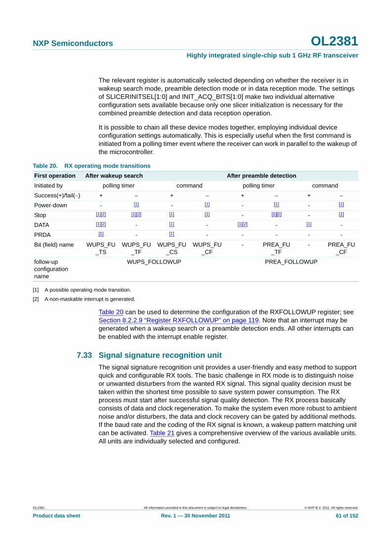
NXP Semiconductors OL2381Highly integrated single-chip sub 1 GHz RF transceiver
The relevant register is automatically selected depending on whether the receiver is in wakeup search mode, preamble detection mode or in data reception mode. The settings of SLICERINITSEL[1:0] and INIT_ACQ_BITS[1:0] make two individual alternative configuration sets available because only one slicer initialization is necessary for the combined preamble detection and data reception operation.
It is possible to chain all these device modes together, employing individual device configuration settings automatically. This is especially useful when the first command is initiated from a polling timer event where the receiver can work in parallel to the wakeup of the microcontroller.
[1] A possible operating mode transition.
[2] A non-maskable interrupt is generated.
Table 20 can be used to determine the configuration of the RXFOLLOWUP register; see Section 8.2.2.9 “Register RXFOLLOWUP” on page 119. Note that an interrupt may be generated when a wakeup search or a preamble detection ends. All other interrupts can be enabled with the interrupt enable register.
7.33 Signal signature recognition unit
The signal signature recognition unit provides a user-friendly and easy method to support quick and configurable RX tools. The basic challenge in RX mode is to distinguish noise or unwanted disturbers from the wanted RX signal. This signal quality decision must be taken within the shortest time possible to save system power consumption. The RX process must start after successful signal quality detection. The RX process basically consists of data and clock regeneration. To make the system even more robust to ambient noise and/or disturbers, the data and clock recovery can be gated by additional methods. If the baud rate and the coding of the RX signal is known, a wakeup pattern matching unit can be activated. Table 21 gives a comprehensive overview of the various available units. All units are individually selected and configured.
Table 20. RX operating mode transitions
First operation After wakeup search After preamble detection
Initiated by polling timer command polling timer command
Success(+)/fail() + + + +
Power-down - [1] - [1] - [1] - [1]
Stop [1][2] [1][2] [1] [1] - [1][2] - [1]
DATA [1][2] - [1] - [1][2] - [1] -
PRDA [1] - [1] - - - - -
Bit (field) name WUPS_FU_TS
WUPS_FU_TF
WUPS_FU_CS
WUPS_FU_CF
- PREA_FU_TF
- PREA_FU_CF
follow-up configuration name
WUPS_FOLLOWUP PREA_FOLLOWUP
OL2381 All information provided in this document is subject to legal disclaimers. © NXP B.V. 2011. All rights reserved.
Product data sheet Rev. 1 — 30 November 2011 61 of 152
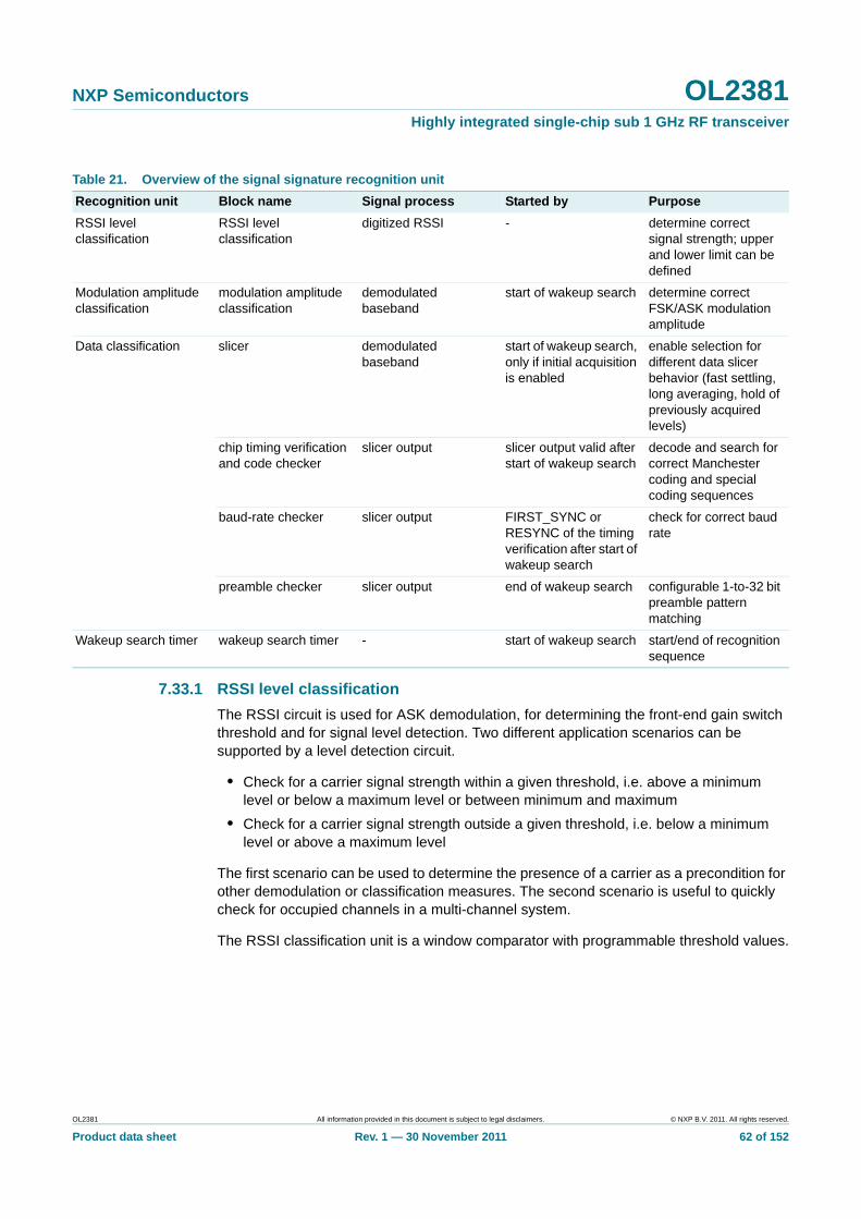
NXP Semiconductors OL2381Highly integrated single-chip sub 1 GHz RF transceiver
7.33.1 RSSI level classification
The RSSI circuit is used for ASK demodulation, for determining the front-end gain switch threshold and for signal level detection. Two different application scenarios can be supported by a level detection circuit.
• Check for a carrier signal strength within a given threshold, i.e. above a minimum level or below a maximum level or between minimum and maximum
• Check for a carrier signal strength outside a given threshold, i.e. below a minimum level or above a maximum level
The first scenario can be used to determine the presence of a carrier as a precondition for other demodulation or classification measures. The second scenario is useful to quickly check for occupied channels in a multi-channel system.
The RSSI classification unit is a window comparator with programmable threshold values.
Table 21. Overview of the signal signature recognition unit
Recognition unit Block name Signal process Started by Purpose
RSSI level classification
RSSI level classification
digitized RSSI - determine correct signal strength; upper and lower limit can be defined
Modulation amplitude classification
modulation amplitude classification
demodulated baseband
start of wakeup search determine correct FSK/ASK modulation amplitude
Data classification slicer demodulated baseband
start of wakeup search, only if initial acquisition is enabled
enable selection for different data slicer behavior (fast settling, long averaging, hold of previously acquired levels)
chip timing verification and code checker
slicer output slicer output valid after start of wakeup search
decode and search for correct Manchester coding and special coding sequences
baud-rate checker slicer output FIRST_SYNC or RESYNC of the timing verification after start of wakeup search
check for correct baud rate
preamble checker slicer output end of wakeup search configurable 1-to-32 bit preamble pattern matching
Wakeup search timer wakeup search timer - start of wakeup search start/end of recognition sequence
OL2381 All information provided in this document is subject to legal disclaimers. © NXP B.V. 2011. All rights reserved.
Product data sheet Rev. 1 — 30 November 2011 62 of 152
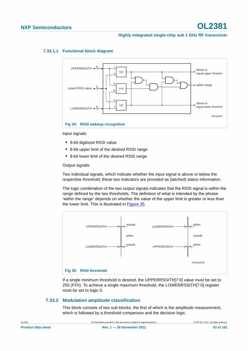
NXP Semiconductors OL2381Highly integrated single-chip sub 1 GHz RF transceiver
7.33.1.1 Functional block diagram
Input signals:
• 8-bit digitized RSSI value
• 8-bit upper limit of the desired RSSI range
• 8-bit lower limit of the desired RSSI range
Output signals:
Two individual signals, which indicate whether the input signal is above or below the respective threshold; these two indicators are provided as (latched) status information.
The logic combination of the two output signals indicates that the RSSI signal is within the range defined by the two thresholds. The definition of what is intended by the phrase ‘within the range’ depends on whether the value of the upper limit is greater or less than the lower limit. This is illustrated in Figure 35.
If a single minimum threshold is desired, the UPPERRSSITH[7:0] value must be set to 255 (FFh). To achieve a single maximum threshold, the LOWERRSSITH[7:0] register must be set to logic 0.
7.33.2 Modulation amplitude classification
This block consists of two sub-blocks, the first of which is the amplitude measurement, which is followed by a threshold comparison and the decision logic.
Fig 34. RSSI wakeup recognition
Fig 35. RSSI threshold
001aan617
8
8
8
UPPERRSSITH
cooked RSSI value
LOWERRSSITH
r
x
x
y
x
r
x<r
x<y
x>r
within range
below orequal upper threshol
above orequal lower threshold
001aan618
UPPERRSSITH
LOWERRSSITH
outside
outside
within
LOWERRSSITH
UPPERRSSITH
within
within
outside
OL2381 All information provided in this document is subject to legal disclaimers. © NXP B.V. 2011. All rights reserved.
Product data sheet Rev. 1 — 30 November 2011 63 of 152
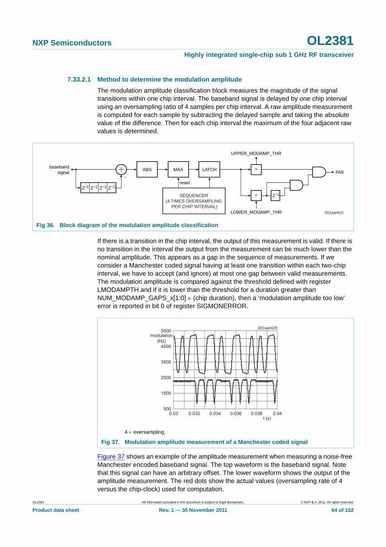
NXP Semiconductors OL2381Highly integrated single-chip sub 1 GHz RF transceiver
7.33.2.1 Method to determine the modulation amplitude
The modulation amplitude classification block measures the magnitude of the signal transitions within one chip interval. The baseband signal is delayed by one chip interval using an oversampling ratio of 4 samples per chip interval. A raw amplitude measurement is computed for each sample by subtracting the delayed sample and taking the absolute value of the difference. Then for each chip interval the maximum of the four adjacent raw values is determined.
If there is a transition in the chip interval, the output of this measurement is valid. If there is no transition in the interval the output from the measurement can be much lower than the nominal amplitude. This appears as a gap in the sequence of measurements. If we consider a Manchester coded signal having at least one transition within each two-chip interval, we have to accept (and ignore) at most one gap between valid measurements. The modulation amplitude is compared against the threshold defined with register LMODAMPTH and if it is lower than the threshold for a duration greater than NUM_MODAMP_GAPS_x[1:0] (chip duration), then a ‘modulation amplitude too low’ error is reported in bit 0 of register SIGMONERROR.
Figure 37 shows an example of the amplitude measurement when measuring a noise-free Manchester encoded baseband signal. The top waveform is the baseband signal. Note that this signal can have an arbitrary offset. The lower waveform shows the output of the amplitude measurement. The red dots show the actual values (oversampling rate of 4 versus the chip-clock) used for computation.
Fig 36. Block diagram of the modulation amplitude classification
001aan619
SEQUENCER (4 TIMES OVERSAMPLING
PER CHIP INTERVAL)
LATCH
LOWER_MODAMP_THR
UPPER_MODAMP_THR
FAILMAX
reset
ABSbasebandsignal
Z−1
>
>
Z−1 Z−1 Z−1
Z−1
−
4 oversampling.
Fig 37. Modulation amplitude measurement of a Manchester coded signal
2500
3500
1500
4500
5500modulation
(Hz)
500
t (s)0.03 0.040.0380.034 0.0360.032
001aan620
OL2381 All information provided in this document is subject to legal disclaimers. © NXP B.V. 2011. All rights reserved.
Product data sheet Rev. 1 — 30 November 2011 64 of 152

NXP Semiconductors OL2381Highly integrated single-chip sub 1 GHz RF transceiver
Due to the ripple in the output signal (lower trace) and the discrete sampling time, the sampled signal can be lower than the theoretical maximum value. Worst case input signals for this algorithm produce a maximum amplitude error of 8 % of the maximum theoretical value.
In this example the upper horizontal dashed line corresponds to the actual amplitude Aact. The lower horizontal dashed line corresponds to Aact 8 % = 0.92 Aact. Consider this when calculating the lower and upper limit for the modulation amplitude detection. The higher limit can be set close to the expected value, the lower limit must be at least 8 % lower than the expected value.
The amplitude measurement for each chip interval is compared with two programmable thresholds. If the measured amplitude is above the upper threshold, the result is immediately classed as a FAIL. If the measured amplitude is below the lower threshold, this can be either a low amplitude condition or a gap. The outcome is a FAIL if two successive amplitude measurements deliver a value which is below the lower threshold; there must be no more than one gap between valid measurements.
The lower and upper thresholds can be independently selected with the 8 bit registers LOWER_MODAMP_TH and UPPER_MODAMP_TH, respectively. The actual threshold value is defined by the associated register settings according to Equation 38.
(38)
Where xxx stands for LOWER_ or UPPER_.
Example: FSK signal Manchester coded, 2 kbit/s respectively 4 kchip/s, modulation deviation: 1.5 kHz.
The FSK signal must be mapped to the output range of the FSK demodulator. The output signal range is 0 to 32256. This range equates to a frequency deviation of 200 kHz respectively 600 kHz, depending on bit LARGE_FM_DEM_RANGE in register EXPERT2. The expected peak-to-peak modulation amplitude is 1.5 / 200 32256 = 242.
The UPPER_MODAMP_TH is set to at least the expected value: 16 24 = 256.
4 oversampling.
Fig 38. Modulation amplitude measurement (zoomed)
001aan621
t (s)0.0343 0.03550.03510.0347
2200
2300
2100
2400
2500modulation
(Hz)
2000
xxxThresholdValue min 2xxx_MODAMP_TH[7:4]
xxx_MODAMP_TH[3:0] 7FFFh =
OL2381 All information provided in this document is subject to legal disclaimers. © NXP B.V. 2011. All rights reserved.
Product data sheet Rev. 1 — 30 November 2011 65 of 152

NXP Semiconductors OL2381Highly integrated single-chip sub 1 GHz RF transceiver
UPPER_MODAMP_TH_MANT[3:0] = 15d = 1111b
UPPER_MODAMP_TH_EXP[7:4] = 4d = 0100b.
The LOWER_MODAMP_TH should be set to 92 % of the maximum expected value: 242 0.92 = 222.
The closest programmable value not exceeding this is 13 24 = 208. Therefore, the LOWER_MODAMP_TH should be programmed as follows:
LOWER _MODAMP_TH_MANT[3:0] = 13d = 1101b
LOWER _MODAMP_TH_EXP[7:4] = 4d = 0100b
The lower and the upper thresholds can be disabled. The lower threshold is disabled by setting LOWER_MODAMP_TH to 0d and the higher threshold is disabled by any value: UPPER_MODAMP_TH 215.
7.34 Data classification
The data slicer is used for the timing, code and baud rate classification modules.
7.34.1 Data slicer
The device features a versatile collection of different data slicers with different initialization and adaptation mechanisms, including:
• an edge-sensitive slicer with minimum latency: used in applications where fast data slicer settling times are crucial
• a level-sensitive slicer: more robust to noise, appropriate when a longer settling time is acceptable
7.34.1.1 Number of corrupted bits in RX mode
The number of corrupted bits during the start of RX mode depends on the selected slicer method and the associated settings. The edge slicer provides the fastest possible settling time, only 1 chip period (1 / 2 bit) is lost. The loss of level-sensitive slicer bits depends on its initialization setting. If the initialization sequence is selected, 4 chips (2 bits) or 16 chips (8 bits) can be lost. It is possible to recover all bits, provided the level sensitive slicer is pre-initialized to the correct threshold.
7.34.1.2 Slicer description
The level-sensitive slicer is configured by the RXDCONx registers; see Section 8.2.1.33 “Register RXDCON0” on page 112. The level slicer threshold can also be initialized with a desired value by programming registers SLICERINITL and SLICERINITH. This could be used to improve level slicer settling time. The actual level slicer threshold currently used can be read from these registers at any time.
OL2381 All information provided in this document is subject to legal disclaimers. © NXP B.V. 2011. All rights reserved.
Product data sheet Rev. 1 — 30 November 2011 66 of 152

NXP Semiconductors OL2381Highly integrated single-chip sub 1 GHz RF transceiver
The edge-sensitive slicer will not make use of these two registers. The EDGE_MODAMP_TH contains the expected peak modulation amplitude with which the edge slicer is initialized. The expected peak modulation value is provided by the EDGE_MODAMP_TH[7:0] register; see Section 8.2.1.32 “Register EMODAMPTH” on page 111. The EDGE_MODAMP_TH is calculated by:
(39)
7.34.2 Edge slicer
The edge slicer operates as a differentiating slicer in combination with a fixed-level slicer. The time-constant is automatically adjusted in accordance with the selected chip rate of the baud-rate generator unit. This slicer is also capable of demodulating NRZ code with long constant bit sequences provided the expected peak modulation amplitude initializes correctly. The basic principle of the edge slicer is explained in Figure 40.
Fig 39. Slicer block diagram
001aan622
READ/WRITEACCESS FROM
SPI
SLICERINITTHR SLICERTHR
LEVEL SLICER
INITIALACQUISITION
EDGE SENSITIVESLICER
basebandsignal
LOW-PASSFILTER
sliceroutput
rx x³r
ThresholdValue 2EDGE_MODAMP_TH[7:4]
EDGE_MODAMP_TH[3:0]=
Fig 40. Working principle of the edge slicer
001aan623
threshold
belowthreshold
a
a
max
min
thresholdat threshold
a
a
max
min
threshold
abovethresholda
a
max
min
OL2381 All information provided in this document is subject to legal disclaimers. © NXP B.V. 2011. All rights reserved.
Product data sheet Rev. 1 — 30 November 2011 67 of 152
NXP Semiconductors OL2381Highly integrated single-chip sub 1 GHz RF transceiver
The slicer operating mode slicer is selected by the slicer selection bits SLICERSEL_W[1:0]; see Table 84 “SLICERSEL_W bit functions” on page 112.
The edge slicer takes five adjacent samples at intervals equivalent to ¼ of the chip width. The four outermost samples (red and blue dots in Figure 40) are used to make up a dynamic threshold and the middle sample (green dot) is compared against this. The threshold value is the average of the maximum and minimum of the four outermost points.
The exact description of the algorithm for the edge slicer is:
1. Consider 5 consecutive samples taken at a distance a ¼ of the chip period width.
2. Compute the minimum and the maximum of all samples except the middle one.
3. Take the average of the maximum and the minimum as the slicer threshold.
4. Compute the maximum and the minimum of the two neighbors of the middle sample.
5. Take the difference of the maximum and the minimum as the amplitude measurement.
6. Compare the measured amplitude against the peak value of the signal which is provided by register EMODAMPTH; see Section 8.2.1.32 “Register EMODAMPTH” on page 111.
7. If the amplitude is above the threshold, set the slicer output according to the comparison of the signal (middle sample) with respect to the slicer threshold.
8. If the amplitude is below the threshold, keep the current state of the slicer output.
The following list summarizes the properties of the edge slicer algorithm:
• Because the input signal needs to be fed through a delay line and because of the necessary linear interpolation the slicer has a delay of about one chip interval.
• Since the slicer acts only on valid signal edges and since it ignores what is between these edges, it can handle arbitrary coded signals, including NRZ.
• The slicer output is valid after the first signal edge and the slicer delay.
• Due to its differentiating function, the edge slicer is more susceptible to noise than slicer threshold generation methods which average over the signal (level-sensitive slicer).
The slicer needs to know the expected amplitude of the baseband signal for amplitude classification, this can be easily provided for FSK signals.
The following configuration settings must be initialized when the edge slicer is used.
Expected peak modulation value: must be provided by the EDGE_MODAMP_TH[7:0] register; see Section 8.2.1.32 “Register EMODAMPTH” on page 111. The EDGE_MODAMP_TH[7:0] value must be calculated using the following procedure:
(40)
Example: FSK signal Manchester coded, 2 kbit/s respectively, 4 kchip/s, modulation deviation: 1.5 kHz.
ThresholdValue 2EDGE_MODAMP_TH[7:4]
EDGE_MODAMP_TH[3:0]=
OL2381 All information provided in this document is subject to legal disclaimers. © NXP B.V. 2011. All rights reserved.
Product data sheet Rev. 1 — 30 November 2011 68 of 152
NXP Semiconductors OL2381Highly integrated single-chip sub 1 GHz RF transceiver
The FSK signal must be mapped to the output range of the FSK demodulator. The output signal range is from 0 to 32256. This range equates to a frequency deviation of 200 kHz to 600 kHz depending on bit LARGE_FM_DEM_RANGE in register EXPERT2. The expected peak modulation amplitude is 1.5 / 200 32256 = 242. The EDGE_MODAMP_TH is set as close as possible to the expected value: 15 24 = 240.
EDGE_MODAMP_TH_MANT[3:0] = 15d = 1111b
EDGE_MODAMP_TH[7:4] = 4d = 0100b
7.34.2.1 Edge slicer signal monitor setting
The lower and upper thresholds for the peak-to-peak amplitude of the baseband signal (FSK modulation) are simply the TX peak-to-peak frequency deviation plus and minus a guard band tolerance (factor of 3 / 4 or 5 / 4) mapped to the output range of the FSK demodulator. They can be calculated with the following equations:
Register LMODAMPTH = 3000 (32256 / 200000) (3 / 4) = 362.
Register UMODAMPTH = 3000 (32256 / 200000) (5 / 4) = 605.
Register UMODAMPTH must be set to a value higher than 605 (10 26 = 640).
UMODAMPTH[3:0] = 10d = 1010b
UMODAMPTH[7:4] = 6d = 0110b
Register LMODAMPTH must be set to a value lower than 362 (11 25 = 352).
LMODAMPTH[3:0] = 11d = 1011b
LMODAMPTH[7:4] = 5d = 0101b
Remark: the amplitude threshold must be set to the expected peak amplitude value.
7.34.3 Level-sensitive slicer
The level-sensitive slicer offers various features which can be configured to improve noise immunity or to reduce latency; see Section 8.2.1.33 “Register RXDCON0” on page 112.
These include:
• User-definable initialization value
• Initial acquisition of the threshold by averaging the baseband signal over 2, 4, and 8 bits
• Continuously variable threshold configured according to output from 1st-order low-pass filter
The slicer operating mode is selected with slicer selection bits SLICERSEL_x[1:0] according to Table 84 “SLICERSEL_W bit functions” on page 112.
The time-constant for the low-pass filter is derived from the baud-rate generator settings. It is assumed that a Manchester encoded single bit comprises two chips.
OL2381 All information provided in this document is subject to legal disclaimers. © NXP B.V. 2011. All rights reserved.
Product data sheet Rev. 1 — 30 November 2011 69 of 152

NXP Semiconductors OL2381Highly integrated single-chip sub 1 GHz RF transceiver
The various level slicer initialization mechanisms are controlled by bits SLICERINITSEL_x[1:0]. If the slicer is initialized, its output becomes invalid for at least one cycle, which restarts the deglitcher and the edge detector. The output remains valid even when the slicer threshold is updated after the initial acquisition refines its threshold value (after 4 and 8 bits).
7.34.3.1 Level-sensitive slicer initial acquisition
The initial acquisition generates a first estimate of the threshold by averaging the RX baseband signal over a fixed time interval of two bits. If a constant 0 or 1 sequence or an alternating 01 sequence is received, the expected value of the error is exactly zero. If a Manchester encoded signal is being received, the maximum error can be ¼ of the whole swing, which is sufficient for an initial estimation. After having calculated this average, the slicer output changes from UNKNOWN to VALID.
The following samples from the baseband signal are used to improve the initially found threshold. After processing an additional 2-bit interval (4 bits in total), a new average is computed having less uncertainty as the initial value (by a factor 2). This is used as the new slicer threshold. Once an additional 4-bit interval is accumulated, having processed 8 bits in total, the final, more accurate estimate for the threshold can be calculated. This threshold value can be read via register SLICERINITH. Register SLICERINITL is automatically updated every time a new initial slicer threshold is available.
It is possible that the 2-bit interval period used for the initial estimate lies in a time period where there is either no RF, RF with only CW (no modulation) or the frame start containing Manchester code violations. In this case the slicer output may have no edges for a long time interval, which may indicate an incorrectly chosen threshold value. If the timing verification block detects a timeout (time interval between edges > 3.5 chip width) it makes sense to reset the threshold estimation in order to get a better initial threshold value. The slicer’s output is again UNKNOWN after the reset for the next 2-bit interval. The slicer’s output becomes VALID again and the classification of its output edges may provide successful data reception. If the RX signal is not usable the slicer may be reset several times until the selected RX operation is aborted.
If the initial acquisition is not used during the wakeup search, it might be useful to disable the auto-reset feature mentioned above. This can be accomplished by a dedicated setting in register SLICERINITSEL.
The initial acquisition operation always inhibits the use of the slicer output (status UNKNOWN) during the calculation of the first two bits, regardless of whether the initial acquisition was triggered for the first time (by an RX event) or if it was re-triggered from a bit timeout.
The initial acquisition updates the slicer initialization register and the slicer register after the calculation of 2, 4, and 8 bits (selected by INIT_ACQ_BITS) provided the RX event was not interrupted by the higher-level state machine. In these circumstances the initial acquisition is stopped to avoid unwanted data corrupting the calculation of the threshold.
Access register SLICERINITH only via the SPI if the initial acquisition is not active. Failure to comply with this may result in the reading of unstable values and the content of register SLICERINITH may become undefined.
OL2381 All information provided in this document is subject to legal disclaimers. © NXP B.V. 2011. All rights reserved.
Product data sheet Rev. 1 — 30 November 2011 70 of 152
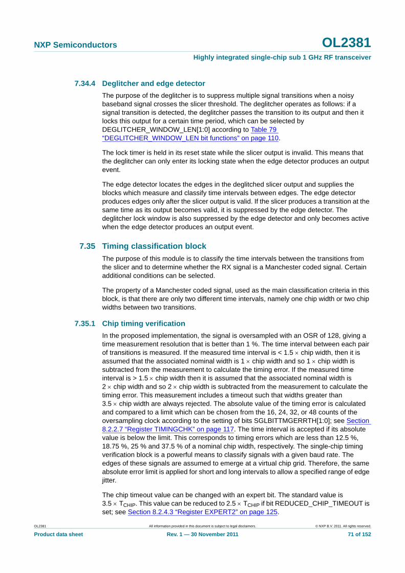
NXP Semiconductors OL2381Highly integrated single-chip sub 1 GHz RF transceiver
7.34.4 Deglitcher and edge detector
The purpose of the deglitcher is to suppress multiple signal transitions when a noisy baseband signal crosses the slicer threshold. The deglitcher operates as follows: if a signal transition is detected, the deglitcher passes the transition to its output and then it locks this output for a certain time period, which can be selected by DEGLITCHER_WINDOW_LEN[1:0] according to Table 79 “DEGLITCHER_WINDOW_LEN bit functions” on page 110.
The lock timer is held in its reset state while the slicer output is invalid. This means that the deglitcher can only enter its locking state when the edge detector produces an output event.
The edge detector locates the edges in the deglitched slicer output and supplies the blocks which measure and classify time intervals between edges. The edge detector produces edges only after the slicer output is valid. If the slicer produces a transition at the same time as its output becomes valid, it is suppressed by the edge detector. The deglitcher lock window is also suppressed by the edge detector and only becomes active when the edge detector produces an output event.
7.35 Timing classification block
The purpose of this module is to classify the time intervals between the transitions from the slicer and to determine whether the RX signal is a Manchester coded signal. Certain additional conditions can be selected.
The property of a Manchester coded signal, used as the main classification criteria in this block, is that there are only two different time intervals, namely one chip width or two chip widths between two transitions.
7.35.1 Chip timing verification
In the proposed implementation, the signal is oversampled with an OSR of 128, giving a time measurement resolution that is better than 1 %. The time interval between each pair of transitions is measured. If the measured time interval is < 1.5 chip width, then it is assumed that the associated nominal width is 1 chip width and so 1 chip width is subtracted from the measurement to calculate the timing error. If the measured time interval is > 1.5 chip width then it is assumed that the associated nominal width is 2 chip width and so 2 chip width is subtracted from the measurement to calculate the timing error. This measurement includes a timeout such that widths greater than 3.5 chip width are always rejected. The absolute value of the timing error is calculated and compared to a limit which can be chosen from the 16, 24, 32, or 48 counts of the oversampling clock according to the setting of bits SGLBITTMGERRTH[1:0]; see Section 8.2.2.7 “Register TIMINGCHK” on page 117. The time interval is accepted if its absolute value is below the limit. This corresponds to timing errors which are less than 12.5 %, 18.75 %, 25 % and 37.5 % of a nominal chip width, respectively. The single-chip timing verification block is a powerful means to classify signals with a given baud rate. The edges of these signals are assumed to emerge at a virtual chip grid. Therefore, the same absolute error limit is applied for short and long intervals to allow a specified range of edge jitter.
The chip timeout value can be changed with an expert bit. The standard value is 3.5 TCHIP. This value can be reduced to 2.5 TCHIP if bit REDUCED_CHIP_TIMEOUT is set; see Section 8.2.4.3 “Register EXPERT2” on page 125.
OL2381 All information provided in this document is subject to legal disclaimers. © NXP B.V. 2011. All rights reserved.
Product data sheet Rev. 1 — 30 November 2011 71 of 152
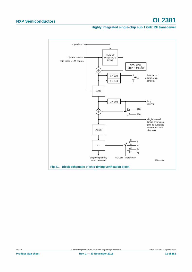
NXP Semiconductors OL2381Highly integrated single-chip sub 1 GHz RF transceiver
Fig 41. Block schematic of chip timing verification block
001aan624
edge detect
chip rate counter
chip width = 128 counts
TIME OFPREVIOUS
EDGE
LATCH
single chip timingerror detected
SGLBITTMGERRTH
ABS()
REDUCED_CHIP_TIMEOUT
interval toolarge, chiptimeout
single intervaltiming error value(will be averagedin the baud-ratechecker)
longinterval
−
−1
0
0
0
1
2
3
1
128
256
8
16
24
32
≥ = 320
≥ = 448
≥ =
≥ = 192
OL2381 All information provided in this document is subject to legal disclaimers. © NXP B.V. 2011. All rights reserved.
Product data sheet Rev. 1 — 30 November 2011 72 of 152
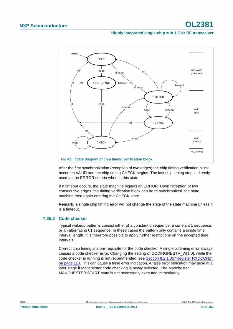
NXP Semiconductors OL2381Highly integrated single-chip sub 1 GHz RF transceiver
After the first synchronization (reception of two edges) the chip timing verification block becomes VALID and the chip timing CHECK begins. The last chip timing step is directly used as the ERROR criteria when in this state.
If a timeout occurs, the state machine signals an ERROR. Upon reception of two consecutive edges, the timing verification block can be re-synchronized, the state machine then again entering the CHECK state.
Remark: a single chip timing error will not change the state of the state machine unless it is a timeout.
7.35.2 Code checker
Typical wakeup patterns consist either of a constant 0 sequence, a constant 1 sequence, or an alternating 01 sequence. In these cases the pattern only contains a single time interval length. It is therefore possible to apply further restrictions on the accepted time intervals.
Correct chip timing is a pre-requisite for the code checker. A single bit timing error always causes a code checker error. Changing the setting of CODINGRESTR_W[1:0], while the code checker is running is not recommended; see Section 8.2.1.35 “Register RXDCON2” on page 113. This can cause a false error indication. A false error indication may arise at a later stage if Manchester code checking is newly selected. The Manchester MANCHESTER START state is not necessarily executed immediately.
Fig 42. State diagram of chip timing verification block
001aan625
CHECKedge
RESYNC
TIMEOUT
timeoutedge
IDLE
reset
edge
FIRST_SYNC
not validunknown
validerror
validok/error
edge
off
off
off
off
timeout
timeout
edge
timeout
timeout
off
off
timeout
OL2381 All information provided in this document is subject to legal disclaimers. © NXP B.V. 2011. All rights reserved.
Product data sheet Rev. 1 — 30 November 2011 73 of 152
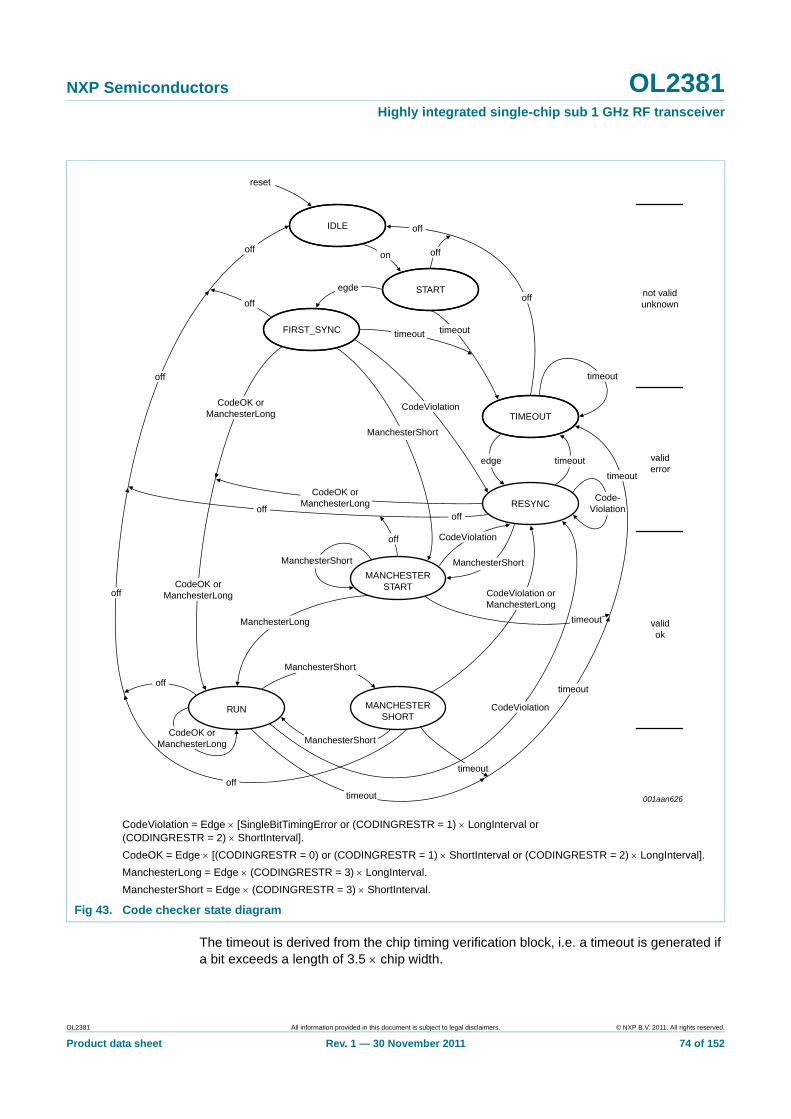
NXP Semiconductors OL2381Highly integrated single-chip sub 1 GHz RF transceiver
The timeout is derived from the chip timing verification block, i.e. a timeout is generated if a bit exceeds a length of 3.5 chip width.
CodeViolation = Edge [SingleBitTimingError or (CODINGRESTR = 1) LongInterval or(CODINGRESTR = 2) ShortInterval].
CodeOK = Edge [(CODINGRESTR = 0) or (CODINGRESTR = 1) ShortInterval or (CODINGRESTR = 2) LongInterval].
ManchesterLong = Edge (CODINGRESTR = 3) LongInterval.
ManchesterShort = Edge (CODINGRESTR = 3) ShortInterval.
Fig 43. Code checker state diagram
001aan626
MANCHESTERSTART
MANCHESTERSHORT
RUN
RESYNC
TIMEOUT
timeoutedge
IDLE
reset
START not validunknown
validerror
validok
FIRST_SYNC
timeout
off
off
off
off
offoff
off
off
off
off
CodeOK orManchesterLong
CodeViolation orManchesterLong
CodeOK orManchesterLong
CodeOK orManchesterLong
ManchesterShort
ManchesterShort
ManchesterLong
ManchesterShort
ManchesterShort
ManchesterShort
CodeOK orManchesterLong
on off
off
CodeViolation
CodeViolation
CodeViolation
Code-Violation
egde
timeouttimeout
timeout
timeout
timeout
timeout
timeout
OL2381 All information provided in this document is subject to legal disclaimers. © NXP B.V. 2011. All rights reserved.
Product data sheet Rev. 1 — 30 November 2011 74 of 152
NXP Semiconductors OL2381Highly integrated single-chip sub 1 GHz RF transceiver
The OK/ERROR information is directly derived from the state machine. The RESYNC state is initiated after a code violation is recognized by any of the other states, unlike the chip timing verification block which only enters the RESYNC state after the occurrence of a timeout.
If CODINGRESTR_W[1:0] is set, it is only possible to differentiate between a run of zeros or a run of ones (short time intervals) if the first long time interval is received, thus determining if the data represents a 01 or a 10 transition. Once the long time interval is received, the remaining sequence can be checked against Manchester coding rules. After a long interval is detected, short intervals must always be in pairs; the following sequence is illegal: SSSSSLLSSLSSSSLSSSL.
7.35.3 Baud-rate checker
An averaging facility is implemented to increase the accuracy of the single time interval check and baud-rate detection by a factor of 4. This averaging is performed on blocks of 8 bits, where the first block starts whenever the chip timing block reaches either FIRST_SYNC state or RESYNC state. Correct timing of a single bit is a prerequisite for the baud-rate checker, therefore averaging is restarted even if a single bit timing error occurs.
The baud-rate checker has no information about the coding of the signal. Thus it is possible that a sequence of 8 bits comprises 17 instead of 16 chips, e.g. if 15 short intervals followed by one long interval are to be examined. If a sequence of several 8-bit blocks is assessed, the accumulated timing uncertainty is never more than 1 chip.
Averaging over 16 chips requires dividing the sum of the individual timing errors by 16, thus causing an unnecessary loss of precision. Therefore the division is omitted and only the timing errors are summed during an 8-bit block. The product of the 8 bits is compared against a limit which can be selected by SUMBITTMGERRTH[2:0] according to Table 100 “SUMBITTMGERRTH bit functions” on page 117.
This block can be easily extended to allow the number of observed bits to be adjusted to either 8, 16, 24 or 32 bits according to the baud rate observation length setting BROBSLENGTH[1:0]; see Table 99 “BROBSLENGTH bit functions” on page 117.
The output of the baud-rate checker is only VALID after the absolute value of the sum of the received 8 bits is checked against the limit. The output immediately signals an ERROR if the limit is violated. If the sum value is within the limit, the measurement proceeds until either a limit violation is detected or the requested number of bits are observed. In the latter case the output becomes VALID and signals OK.
The baud-rate checker continues checking on an 8-bit basis after the requested number of bits was checked successfully. The ERROR signal is updated at the end of every 8-bit sequence. It stays VALID and OK if the baud rate is within the limit. If the baud rate is outside the limit, an ERROR is signaled and the baud-rate checker restarts. The ERROR signal is retained as long as no 8-bit sequence is within the limit. If the selected observation length is greater than 8 bits, the baud-rate checker enters the NOT VALID state as soon as the first correct 8-bit sequence is received and finally signals VALID and OK after successful reception of the selected observation length. This mechanism assures that the baud-rate checker can only signal VALID and OK once the selected number of consecutive bits are received with the correct baud rate.
OL2381 All information provided in this document is subject to legal disclaimers. © NXP B.V. 2011. All rights reserved.
Product data sheet Rev. 1 — 30 November 2011 75 of 152
NXP Semiconductors OL2381Highly integrated single-chip sub 1 GHz RF transceiver
On the occurrence of a timeout or a single bit timing error, the baud-rate checker resets immediately, NOT VALID is signaled instantaneously and the baud-rate checker restarts.
7.35.4 Timeout timer for the wakeup search
The control logic includes a timeout timer for the wakeup search operation. When used, this timer generates a negative wakeup detection output provided a positive wakeup detection is not generated prior to the timer expiration. When this timer is disabled, the output of the wakeup search operation is instantly negative upon a failure signal from any of the detection operations.
The wakeup search timer consists of a prescaler and a timer register. The clock is derived from the mainscaler clock and is therefore associated with the selected baud rate.
The timeout can be selected by WUPSTIMEOUT[5:0] and is calculated as WUPSTIMEOUT5:0] TWUPSTO for WUPSTIMEOUT[5:0] = 1 to 63d.
The value WUPSTIMEOUT[5:0] = 0 disables the timeout timer and selects an infinite timeout.
The generated timeout has an uncertainty of 2 to 0 TBIT regardless of the setting of WUPSTIMEOUTPRESC[1:0] and WUPSTIMEOUT[5:0].
Timeout timer resolution and range:
• The fastest bit rate of 50 kbit/s requires the timeout to be adjusted in a range of 40 s up to 80 ms with a resolution of 40 s, 80 s, 320 s, and 1.28 ms respectively.
• A bit rate of 1 kbit/s requires the timeout to be adjusted in a range of 2 ms up to 4 s with a resolution of 2 ms, 4 ms, 16 ms, and 64 ms respectively; see Section 8.2.2.4 “Register WUPSTO” on page 116.
7.36 Wakeup search logic
A summary of the signal monitoring conditions which can be used as wakeup criteria are shown in Table 22.
Fig 44. Wakeup search timeout timer schematic
001aan627
PRESCALER
WAKEUP SEARCHTIMEOUT TIMER
:2 :4 :16 :64
00 01 10 11
CLKBit
WUPSTIMEOUTPRESC
WUPSTIMEOUT
wakeup searchtimeout
CLKWUPSTO
OL2381 All information provided in this document is subject to legal disclaimers. © NXP B.V. 2011. All rights reserved.
Product data sheet Rev. 1 — 30 November 2011 76 of 152
NXP Semiconductors OL2381Highly integrated single-chip sub 1 GHz RF transceiver
At the start of a wakeup search the following blocks are reset:
• wakeup search timer
• modulation amplitude classification
• chip timing verification and code checker
• baud-rate checker
• the slicer (conditionally)
The slicer is only reset if configured to acquire the value from the slicer initialization register (SLICERINITSEL_x[1:0] not equal to 00b). If slicer initial acquisition is selected, the chip timing verification, code checker block and baud-rate checker are held in the reset state for the duration of the slicer initial acquisition mode.
Register SIGMON_EN_W[5:0] provides enable bits which determine signal monitors that are considered for the overall wakeup detection decision; see Section 8.2.2.1 “Signal monitoring register SIGMON0” on page 114. All signal monitors operate regardless of these enable bits and, after the wakeup search ends, their results are available in the corresponding status bits. Section 7.36.1 and Section 7.36.2 describe how the individual results from several signal monitors can be combined to achieve an overall wakeup decision.
Each of the signal monitors can have an invalid period caused by an initialization or resynchronization during which the output result is not considered. The logic depicted in Figure 45 shows how this information is translated into the PASS/FAIL condition used by the wakeup search logic. If a signal monitor is in its invalid state, neither a PASS or FAIL condition is generated. If a signal monitor is not selected for the wakeup search, the FAIL is always zero and the PASS always one. The PASS and FAIL signals are exclusively used for the wakeup search logic and they must not be confused with the actual state of the corresponding signal monitor (signals VALID and ERROR) which can be observed in registers SIGMONSTATUS and SIGMONERROR; see Section 8.2.2.10 “Register SIGMONSTATUS” on page 121.
Table 22. Overview of signal monitoring methods
Block name Processes the signal Started by Output is valid after Can be started by
RSSI level classification
digitized RSSI - input is valid -
Modulation amplitude classification
demodulated baseband
start of wakeup search 2 chips -
Slicer start of wakeup search only if initial acquisition is enabled
2 bits if initial acquisition, otherwise immediately
timeout from chip timing verification, only if enabled and in mode 2
Chip timing verification and code checker
slicer output slicer output valid after start of wakeup search
0 < t <5 chips (2 chip time-outs)
in mode 2 by the slicer, only if initial acquisition is enabled
Baud-rate checker FIRST_SYNC or RESYNC of the timing verification after start of wakeup search
8 bits t configured observation length (8, 16, 24 or 32 bits)
in mode 2 by the chip timing verification with another FIRST_SYNC or RESYNC
Wakeup search timer - start of wakeup search FAIL after configured timeout
-
OL2381 All information provided in this document is subject to legal disclaimers. © NXP B.V. 2011. All rights reserved.
Product data sheet Rev. 1 — 30 November 2011 77 of 152
NXP Semiconductors OL2381Highly integrated single-chip sub 1 GHz RF transceiver
Two different mechanisms are provided for the wakeup search:
• ‘pessimistic wakeup search’ or mode 1
• ‘optimistic wakeup search’ or mode 2
In the pessimistic wakeup search (mode 1) the wakeup search timer has no meaning and therefore will not influence the result. In the optimistic wakeup search (mode 2) the wakeup search timer is always active.
At the end of the wakeup search an interrupt request is generated and the result is stored in bit WUPSFAIL. If this bit is set, it signals that the wakeup criteria was not met. Otherwise it is cleared. The content of this bit is undefined prior to first use of the wakeup search.
The polarity of bit WUPSFAIL is chosen so that register SIGMONSTATUS can be used as a mask for register SIGMONERROR when the host controller is interested in retrieving the cause of an unsuccessful wakeup detection. If the wakeup search was successful (bit WUPSFAIL is cleared) the content of register SIGMONERROR is not required to be considered as all relevant bits are cleared.
Fig 45. Creation of PASS/FAIL information from one signal monitor
Fig 46. Block diagram of wakeup search
001aan628
validfail
passerror
WUPS_EN[i]
001aan629
WAKEUP SEARCHTIMER
RSSI LEVELCLASSIFICATION
MODULATION AMP.CLASSIFICATION
CHIP TIMINGCLASSIFICATION
CODECHECKER
BAUD-RATECHECKER
timeout
interrupt request:wakeup searchfinished
WUPSFAIL
WUPSMODE
fail
wakeupdetected
pass
fail
pass
fail
pass
fail
pass
fail
pass
OL2381 All information provided in this document is subject to legal disclaimers. © NXP B.V. 2011. All rights reserved.
Product data sheet Rev. 1 — 30 November 2011 78 of 152

NXP Semiconductors OL2381Highly integrated single-chip sub 1 GHz RF transceiver
7.36.1 Sampling the signal monitoring status
Since the information from the OL2381’s signal monitoring method is made up of more than 8 bits, it is desirable to provide a mechanism which ensures that the controller can always retrieve a consistent set of status information. Therefore the OL2381 provides three status registers: SIGMONSTATUS, SIGMONERROR and RSSILEVEL into which the status is simultaneously transferred, whenever it is either actively requested by the controller or automatically saved by the wakeup search logic; see Section 8.2.2.12 “Register RSSILEVEL” on page 122.
There are two cases in which the status is sampled:
• after a read command, regardless of the address that follows, but only if bit STATAUTOSAMPLE is set; see Section 8.2.2.8 “Register RXCON” on page 118
• always at the end of a wakeup search
Bit STATAUTOSAMPLE either allows software to control the sampling of the status information with each read command (logic 1) or allows the status to be unaffected by any read command (logic 0). This allows consistent read and write command status information to be read as shown by the examples given in Table 23 and Table 24.
Fig 47. Wakeup search registers
001aan630
WUP TIMEOUT
CHIP TIMEOUT
CHIP TIMING
CODING
BAUD RATE
RSSI LEVEL
MODULATION AMPLITUDE TOO HIGH
WUPSFAIL
MODULATION AMPLITUDE TOO LOW
WUPSMODE
SIGMONERRORSIGMONSTATUS
WUPS_EN
status registeraddress k + 1
status register ataddress k
validindicators
control register
RFU
Table 23. Example 1: Using single byte reads
Command Description
Write (STATAUTOSAMPLE, 1) enable status sampling with the next read
Read (SIGMONSTATUS) this samples the consistent status
Write (STATAUTOSAMPLE, 0) disable status sampling with the next reads
Read (SIGMONERROR) consistent with line 2
Read (RSSILEVEL) consistent with line 2
Read (SIGMONSTATUS) reads the same as line 2
Read (RSSILEVEL) reads the same as line 5
Read (SIGMONERROR) reads the same as line 4
OL2381 All information provided in this document is subject to legal disclaimers. © NXP B.V. 2011. All rights reserved.
Product data sheet Rev. 1 — 30 November 2011 79 of 152
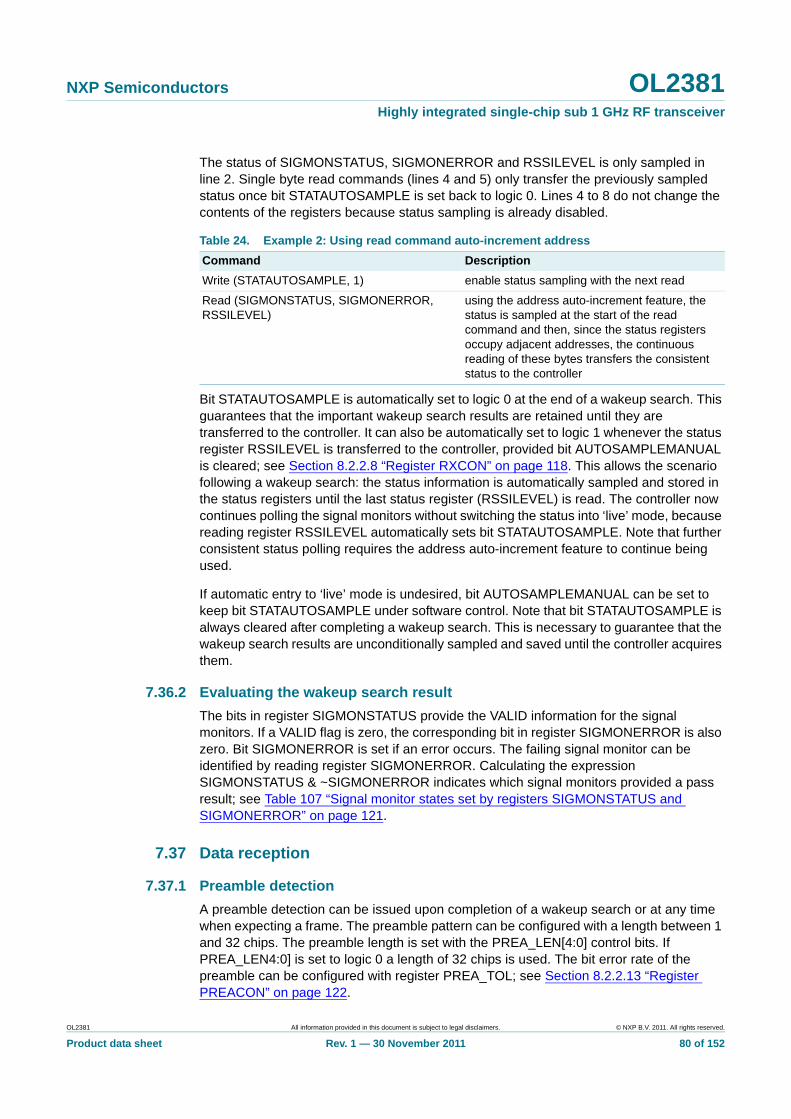
NXP Semiconductors OL2381Highly integrated single-chip sub 1 GHz RF transceiver
The status of SIGMONSTATUS, SIGMONERROR and RSSILEVEL is only sampled in line 2. Single byte read commands (lines 4 and 5) only transfer the previously sampled status once bit STATAUTOSAMPLE is set back to logic 0. Lines 4 to 8 do not change the contents of the registers because status sampling is already disabled.
Bit STATAUTOSAMPLE is automatically set to logic 0 at the end of a wakeup search. This guarantees that the important wakeup search results are retained until they are transferred to the controller. It can also be automatically set to logic 1 whenever the status register RSSILEVEL is transferred to the controller, provided bit AUTOSAMPLEMANUAL is cleared; see Section 8.2.2.8 “Register RXCON” on page 118. This allows the scenario following a wakeup search: the status information is automatically sampled and stored in the status registers until the last status register (RSSILEVEL) is read. The controller now continues polling the signal monitors without switching the status into ‘live’ mode, because reading register RSSILEVEL automatically sets bit STATAUTOSAMPLE. Note that further consistent status polling requires the address auto-increment feature to continue being used.
If automatic entry to ‘live’ mode is undesired, bit AUTOSAMPLEMANUAL can be set to keep bit STATAUTOSAMPLE under software control. Note that bit STATAUTOSAMPLE is always cleared after completing a wakeup search. This is necessary to guarantee that the wakeup search results are unconditionally sampled and saved until the controller acquires them.
7.36.2 Evaluating the wakeup search result
The bits in register SIGMONSTATUS provide the VALID information for the signal monitors. If a VALID flag is zero, the corresponding bit in register SIGMONERROR is also zero. Bit SIGMONERROR is set if an error occurs. The failing signal monitor can be identified by reading register SIGMONERROR. Calculating the expression SIGMONSTATUS & ~SIGMONERROR indicates which signal monitors provided a pass result; see Table 107 “Signal monitor states set by registers SIGMONSTATUS and SIGMONERROR” on page 121.
7.37 Data reception
7.37.1 Preamble detection
A preamble detection can be issued upon completion of a wakeup search or at any time when expecting a frame. The preamble pattern can be configured with a length between 1 and 32 chips. The preamble length is set with the PREA_LEN[4:0] control bits. If PREA_LEN4:0] is set to logic 0 a length of 32 chips is used. The bit error rate of the preamble can be configured with register PREA_TOL; see Section 8.2.2.13 “Register PREACON” on page 122.
Table 24. Example 2: Using read command auto-increment address
Command Description
Write (STATAUTOSAMPLE, 1) enable status sampling with the next read
Read (SIGMONSTATUS, SIGMONERROR, RSSILEVEL)
using the address auto-increment feature, the status is sampled at the start of the read command and then, since the status registers occupy adjacent addresses, the continuous reading of these bytes transfers the consistent status to the controller
OL2381 All information provided in this document is subject to legal disclaimers. © NXP B.V. 2011. All rights reserved.
Product data sheet Rev. 1 — 30 November 2011 80 of 152

NXP Semiconductors OL2381Highly integrated single-chip sub 1 GHz RF transceiver
7.38 RX data decoding
After a wakeup search, if configured, a preamble detection and data reception follows seamlessly. After successful completion of the wakeup search and the preamble detection, the RX data is switched to the corresponding port pins, dependent on the device configuration. The data pin is kept LOW during wakeup search and HIGH during preamble detection. Data reception can be interleaved with SPI commands. Details are given in Section 7.32.2 “Receive command” on page 55. The device has a Manchester code recovery feature which enables inversion of the RX data. The precondition of this code recovery unit is the full reception of a Manchester data stream with at least one polarity change within the code. The accumulated sum of data changes within a chip can be found in the MANCHESTER_COUNT[3:0] field in register EXTRXSTATUS; see Section 8.2.3.1 “Register EXTRXSTATUS” on page 123. This is a 4-bit signed number which is applicable only when receiving data through the Manchester decoder. It is not needed if the frame start is properly synchronized with a preamble detection. If data reception is initiated with the DATA sub-command (without preamble detection), the Manchester decoding starts at the first chip it gets, without knowing whether this is the left or the right bit half. The RX data line can deliver the data correctly or inverted. If the signal contains any bit transitions, this counter counts up if the transition occurs at the assumed bit boundary (i.e. when it is correct) and it counts down if the transition occurs in the middle of the assumed bit grid (i.e. when it is incorrect). The result is that bit 3 of this counter is logic 0 if the data is decoded properly and it is logic 1 if the data is delivered inverted. The whole counter stays at zero if the RX signal contains no bit transitions, in which case it is not possible to tell whether the RX data is a long run of only zeros or a run of ones. If the sum is negative, the RX code must be treated as inverted, if the sum is positive, the data reception was correct. It is possible to invert the RX data stream by setting bit INV_RX_DATA; see Section 7.13.1 “Clock recovery for RX mode” on page 29.
If the receiver is configured transparently (see register RXCON), the data pin is directly switched to the selected data slicer and mapped to the corresponding port pin after the RX command is issued.
7.39 RX clock generation
After a wakeup search, if configured, a preamble detection and clock recovery operate in parallel. Allow sufficient settling time from the start of data reception to the successful recovery of a stable clock. The run-in time (wakeup time and length of preamble) must be longer than the programmed settling time without code timing violations in-between the different phases to ensure correct operation. After successful completion of the wakeup search and the preamble detection, the bit or chip clock is switched to the corresponding port pin, depending on the device configuration. During wakeup search and preamble detection, the clock pin is kept at a constant HIGH. Data reception can be interleaved by SPI commands. Details are given in Section 7.32.2 “Receive command” on page 55.
If bit RX_MANCHESTER is set, the clock rate is set to the bit rate so that every second chip is sampled at the correct time; see Section 8.2.2.8 “Register RXCON” on page 118. This enables the microcontroller to directly decode the Manchester bit stream by sampling the RX data with the negative clock edges.
If the receiver is configured in a transparent mode, the clock pin is directly switched to clock recovery and mapped to the corresponding port pin after the RX command is issued.
OL2381 All information provided in this document is subject to legal disclaimers. © NXP B.V. 2011. All rights reserved.
Product data sheet Rev. 1 — 30 November 2011 81 of 152
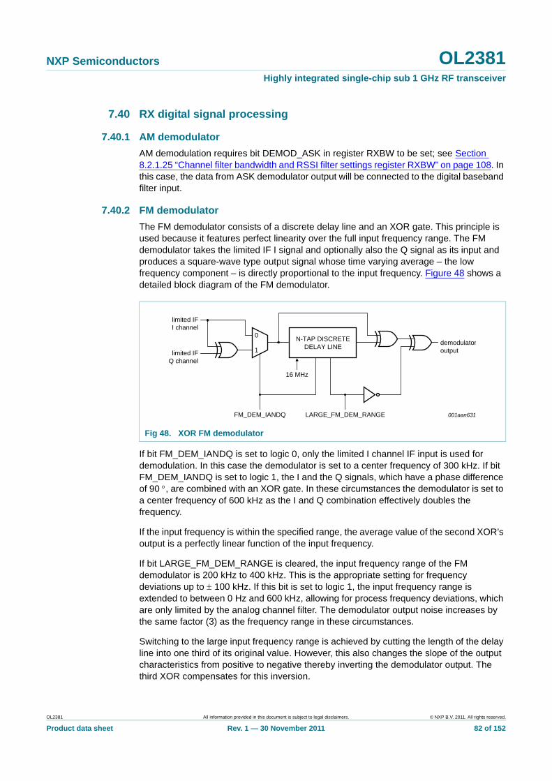
NXP Semiconductors OL2381Highly integrated single-chip sub 1 GHz RF transceiver
7.40 RX digital signal processing
7.40.1 AM demodulator
AM demodulation requires bit DEMOD_ASK in register RXBW to be set; see Section 8.2.1.25 “Channel filter bandwidth and RSSI filter settings register RXBW” on page 108. In this case, the data from ASK demodulator output will be connected to the digital baseband filter input.
7.40.2 FM demodulator
The FM demodulator consists of a discrete delay line and an XOR gate. This principle is used because it features perfect linearity over the full input frequency range. The FM demodulator takes the limited IF I signal and optionally also the Q signal as its input and produces a square-wave type output signal whose time varying average – the low frequency component – is directly proportional to the input frequency. Figure 48 shows a detailed block diagram of the FM demodulator.
If bit FM_DEM_IANDQ is set to logic 0, only the limited I channel IF input is used for demodulation. In this case the demodulator is set to a center frequency of 300 kHz. If bit FM_DEM_IANDQ is set to logic 1, the I and the Q signals, which have a phase difference of 90 , are combined with an XOR gate. In these circumstances the demodulator is set to a center frequency of 600 kHz as the I and Q combination effectively doubles the frequency.
If the input frequency is within the specified range, the average value of the second XOR’s output is a perfectly linear function of the input frequency.
If bit LARGE_FM_DEM_RANGE is cleared, the input frequency range of the FM demodulator is 200 kHz to 400 kHz. This is the appropriate setting for frequency deviations up to 100 kHz. If this bit is set to logic 1, the input frequency range is extended to between 0 Hz and 600 kHz, allowing for process frequency deviations, which are only limited by the analog channel filter. The demodulator output noise increases by the same factor (3) as the frequency range in these circumstances.
Switching to the large input frequency range is achieved by cutting the length of the delay line into one third of its original value. However, this also changes the slope of the output characteristics from positive to negative thereby inverting the demodulator output. The third XOR compensates for this inversion.
Fig 48. XOR FM demodulator
001aan631
N-TAP DISCRETEDELAY LINE
FM_DEM_IANDQ LARGE_FM_DEM_RANGE
demodulatoroutput
limited IFI channel
0
1limited IFQ channel
16 MHz
OL2381 All information provided in this document is subject to legal disclaimers. © NXP B.V. 2011. All rights reserved.
Product data sheet Rev. 1 — 30 November 2011 82 of 152

NXP Semiconductors OL2381Highly integrated single-chip sub 1 GHz RF transceiver
7.40.3 Baseband filter
The baseband filter serves the following purposes:
• suppresses the high frequency (square-wave) components from the FM demodulator, leaving only the time-varying average, or baseband component of the demodulated signal
• suppresses spectral portions of the quantization noise from the demodulator and the demodulated noise coming from the RF input which do not fall into the baseband signal’s bandwidth
• helps achieve a suitable sampling rate for further processing of the baseband signal
The baseband filter is a 3rd-order IIR filter topology that is optimized such that it features a step response with almost no ringing as shown in Figure 50.
7.40.3.1 RX baseband configuration
The filter is split into a 1st-order and a 2nd-order section to minimize the internal quantization noise. Figure 49 shows the baseband filter distributed over two filter blocks.
The 1st and 2nd-order sections combine to make the 3rd-order baseband filter for ASK or FSK. The filter cut-off frequency is controlled by register BASEBAND_FILTER_FC control bits; see Section 8.2.1.29 “Register RXBBCON” on page 109. The 1st-order section filters the RSSI information which is sampled with the ADC in the limiter/RSSI analog circuitry. Its cut-off frequency can be controlled separately by register RSSI_FILTER_FC; see Section 8.2.1.25 “Channel filter bandwidth and RSSI filter settings register RXBW” on page 108.
Note that the baseband filter and the RSSI filter are two separate filters.
Table 25. FM demodulator configurationsSee register EXPERT2 bit descriptions in Table 117 on page 125.
D7 D6 Center frequency (kHz)
Input frequency range (kHz)
Maximum frequency deviation (kHz)
Number of delay elements
0 0 300 200 to 400 100 40
0 1 300 0 to 600 300 13
1 0 600 200 to 400 100 20
1 1 600 0 to 600 300 7
Fig 49. Baseband filter signal flow
001aan632
output from FMdemodulator
to basebandprocessingresult from
RSSI ADC
DEMOD_ASK1st-ordersection
BASEBAND_FILTER_FC
1st-ordersection
0
1
DOWN-SAMPLE
2nd-ordersection
OL2381 All information provided in this document is subject to legal disclaimers. © NXP B.V. 2011. All rights reserved.
Product data sheet Rev. 1 — 30 November 2011 83 of 152

NXP Semiconductors OL2381Highly integrated single-chip sub 1 GHz RF transceiver
Figure 50 and Figure 51 show the step response and the frequency response of the baseband filter, respectively. Figure 50 shows that the step response has an undershoot (negative overshoot) of approximately 3 % and an almost unnoticeable overshoot. This demonstrates a characteristic close to that of an analog Bessel filter. Figure 51 contains one frequency response curve for each of the ten implemented cut-off frequency control values (0 to 9).
The accurate output sampling frequency of the data filter can be calculated. The frequency is divided by a factor of 2 when the cut-off frequency control setting is incremented by 1. The relevant formula is:
(41)
It can be seen that each increment in the cut-off frequency control setting divides the corner frequency of the filter by approximately a factor of 2.
Fig 50. Step response of the baseband filter
Fig 51. Frequency response of the baseband filter
0.4
0.8
1.2
amplitude
0
samples0 20016080 12040
001aan633
f (Hz)1 107105 10610410 103102
001aan634
amplitude responses(dB)
0
−20
−40
−60
−80
−100
fc114 kHz
2FskFilterFc
-----------------------=
OL2381 All information provided in this document is subject to legal disclaimers. © NXP B.V. 2011. All rights reserved.
Product data sheet Rev. 1 — 30 November 2011 84 of 152
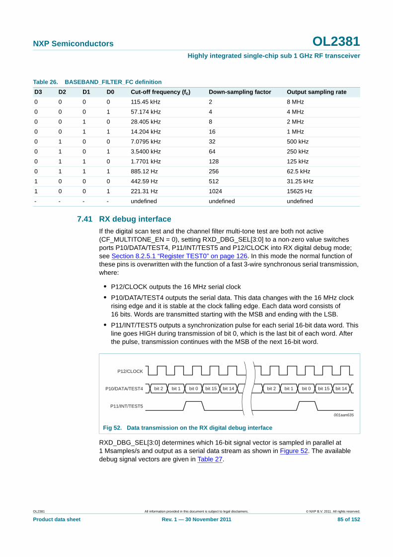
NXP Semiconductors OL2381Highly integrated single-chip sub 1 GHz RF transceiver
7.41 RX debug interface
If the digital scan test and the channel filter multi-tone test are both not active (CF_MULTITONE_EN = 0), setting RXD_DBG_SEL[3:0] to a non-zero value switches ports P10/DATA/TEST4, P11/INT/TEST5 and P12/CLOCK into RX digital debug mode; see Section 8.2.5.1 “Register TEST0” on page 126. In this mode the normal function of these pins is overwritten with the function of a fast 3-wire synchronous serial transmission, where:
• P12/CLOCK outputs the 16 MHz serial clock
• P10/DATA/TEST4 outputs the serial data. This data changes with the 16 MHz clock rising edge and it is stable at the clock falling edge. Each data word consists of 16 bits. Words are transmitted starting with the MSB and ending with the LSB.
• P11/INT/TEST5 outputs a synchronization pulse for each serial 16-bit data word. This line goes HIGH during transmission of bit 0, which is the last bit of each word. After the pulse, transmission continues with the MSB of the next 16-bit word.
RXD_DBG_SEL[3:0] determines which 16-bit signal vector is sampled in parallel at 1 Msamples/s and output as a serial data stream as shown in Figure 52. The available debug signal vectors are given in Table 27.
Table 26. BASEBAND_FILTER_FC definition
D3 D2 D1 D0 Cut-off frequency (fc) Down-sampling factor Output sampling rate
0 0 0 0 115.45 kHz 2 8 MHz
0 0 0 1 57.174 kHz 4 4 MHz
0 0 1 0 28.405 kHz 8 2 MHz
0 0 1 1 14.204 kHz 16 1 MHz
0 1 0 0 7.0795 kHz 32 500 kHz
0 1 0 1 3.5400 kHz 64 250 kHz
0 1 1 0 1.7701 kHz 128 125 kHz
0 1 1 1 885.12 Hz 256 62.5 kHz
1 0 0 0 442.59 Hz 512 31.25 kHz
1 0 0 1 221.31 Hz 1024 15625 Hz
- - - - undefined undefined undefined
Fig 52. Data transmission on the RX digital debug interface
001aan635
P12/CLOCK
P10/DATA/TEST4 bit 2
P11/INT/TEST5
bit 1 bit 0 bit 15 bit 14 bit 2 bit 1 bit 0 bit 15 bit 14
OL2381 All information provided in this document is subject to legal disclaimers. © NXP B.V. 2011. All rights reserved.
Product data sheet Rev. 1 — 30 November 2011 85 of 152

NXP Semiconductors OL2381Highly integrated single-chip sub 1 GHz RF transceiver
Table 27. Available RX debug signal vectors
RXD_DBG_SEL Bit range Signal name Signal description
1 [15:8] w8RssiLevelOut digitized RSSI result as it can be retrieved through the status register RSSI_LEVEL
1 [7] wIFSettledIn indicates when the 300 kHz IF signal is declared stable
1 [6] wRssiSettled indicates when the RSSI result is declared stable
1 [5:0] r6RawRssiAdcValOut raw RSSI ADC readings
2 [15:4] w12FiltdRssi RSSI signal after the 1st order low-pass filter
2 [3] rFrontEndGainLoOut indicates which of the front-end gain settings are applied. 0: RX_HI_GAIN, 1: RX_LO_GAIN
2 [2] wRssiGtUpperTh indicates when the RSSI result is greater than the threshold set with UPPERRSSITH
2 [1] wRssiLtLowerTh indicates when the RSSI result is less than the threshold set with LOWERRSSITH
2 [0] wRssiOutsideLimitsOut indicates when the RSSI is outside the limits defined with both LOWERRSSITH and UPPERRSSITH.
3 [15:4] w12DataFilter1Res baseband signal after the 1st-order section of the baseband filter
3 [3] wLimIfIIn digital IF input from the I channel limiter
3 [2] wLimIfQIn digital IF input from the Q channel limiter
3 [1] wRawXorFmDemod raw, unfiltered output from the XOR FM demodulator
3 [0] wIFSettled indicates when the 300 kHz IF signal is declared stable
4 [15:1] w15BasebandSig filtered and interpolated baseband signal
4 [0] wBasebandValid indicates when the baseband signal is declared valid
5 [15:1] w15SlicerInitThrRegOut contents of the initial slicer threshold register. This is the same as it is available through registers SLICERINITL and SLICERINITH.
5 [0] wLoadInitSlicerThr indicates when the initial threshold register is re-loaded. At chip rates > 7812 chip/s this pulse is shorter than the sampling interval and so pulses may be missed
6 [15:1] w15SlicerThr threshold of the level slicer.
6 [0] wLoadSlicerThr indicates when the threshold is re-loaded. At chip rates > 7812 chip/s this pulse is shorter than the sampling interval and so pulses may be missed.
7 [15:8] ws8ClkRcvPllPhaseError signed clock recovery phase error measurement value in offset binary format.
7 [7:0] - always zero (Reserved)
8 [15] wRxFrame indicates when data is being received
8 [14] wRxData RX data sampled with wRxClock and optionally Manchester decoded
8 [13] wRxClock Recovered bit clock
8 [12] wPatternMatch raw pattern match indicator from the preamble detection block
8 [11] wChipClock raw chip clock from clock recovery PLL
8 [10] wEdgeDetected edge detector output from deglitcher, pulses are shorter than the sampling interval for chip rates > 7812 chip/s so some pulses may be missed
OL2381 All information provided in this document is subject to legal disclaimers. © NXP B.V. 2011. All rights reserved.
Product data sheet Rev. 1 — 30 November 2011 86 of 152
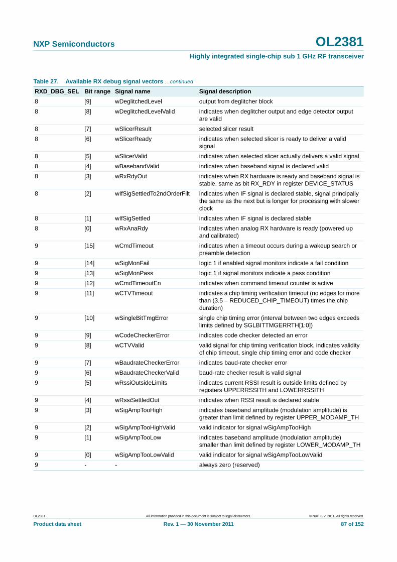
NXP Semiconductors OL2381Highly integrated single-chip sub 1 GHz RF transceiver
8 [9] wDeglitchedLevel output from deglitcher block
8 [8] wDeglitchedLevelValid indicates when deglitcher output and edge detector output are valid
8 [7] wSlicerResult selected slicer result
8 [6] wSlicerReady indicates when selected slicer is ready to deliver a valid signal
8 [5] wSlicerValid indicates when selected slicer actually delivers a valid signal
8 [4] wBasebandValid indicates when baseband signal is declared valid
8 [3] wRxRdyOut indicates when RX hardware is ready and baseband signal is stable, same as bit RX_RDY in register DEVICE_STATUS
8 [2] wIfSigSettledTo2ndOrderFilt indicates when IF signal is declared stable, signal principally the same as the next but is longer for processing with slower clock
8 [1] wIfSigSettled indicates when IF signal is declared stable
8 [0] wRxAnaRdy indicates when analog RX hardware is ready (powered up and calibrated)
9 [15] wCmdTimeout indicates when a timeout occurs during a wakeup search or preamble detection
9 [14] wSigMonFail logic 1 if enabled signal monitors indicate a fail condition
9 [13] wSigMonPass logic 1 if signal monitors indicate a pass condition
9 [12] wCmdTimeoutEn indicates when command timeout counter is active
9 [11] wCTVTimeout indicates a chip timing verification timeout (no edges for more than (3.5 REDUCED_CHIP_TIMEOUT) times the chip duration)
9 [10] wSingleBitTmgError single chip timing error (interval between two edges exceeds limits defined by SGLBITTMGERRTH[1:0])
9 [9] wCodeCheckerError indicates code checker detected an error
9 [8] wCTVValid valid signal for chip timing verification block, indicates validity of chip timeout, single chip timing error and code checker
9 [7] wBaudrateCheckerError indicates baud-rate checker error
9 [6] wBaudrateCheckerValid baud-rate checker result is valid signal
9 [5] wRssiOutsideLimits indicates current RSSI result is outside limits defined by registers UPPERRSSITH and LOWERRSSITH
9 [4] wRssiSettledOut indicates when RSSI result is declared stable
9 [3] wSigAmpTooHigh indicates baseband amplitude (modulation amplitude) is greater than limit defined by register UPPER_MODAMP_TH
9 [2] wSigAmpTooHighValid valid indicator for signal wSigAmpTooHigh
9 [1] wSigAmpTooLow indicates baseband amplitude (modulation amplitude) smaller than limit defined by register LOWER_MODAMP_TH
9 [0] wSigAmpTooLowValid valid indicator for signal wSigAmpTooLowValid
9 - - always zero (reserved)
Table 27. Available RX debug signal vectors …continued
RXD_DBG_SEL Bit range Signal name Signal description
OL2381 All information provided in this document is subject to legal disclaimers. © NXP B.V. 2011. All rights reserved.
Product data sheet Rev. 1 — 30 November 2011 87 of 152
NXP Semiconductors OL2381Highly integrated single-chip sub 1 GHz RF transceiver
8. Special function registers
8.1 Overview
A map of the Special Function Registers (SFR) is shown in Table 28.
The SFRs are arranged into two banks: bank 0 and bank 1. Bank 0 or bank 1 can be selected by setting bit BANK_SEL in register BANKSEL, visible in both banks, accordingly.
Bytes 0 to 2Dh and 3Fh can always be accessed, independent of the setting of bit BANK_SEL in register BANKSEL (3Fh). Clearing bit BANK_SEL enables bytes 2Eh to 3Eh in bank 0; the contents of bank 1 remain unchanged. Setting register BANKSEL activates bytes 2Eh to 3Eh in bank 1.
Reading from a status register returns the current status of the device. Writing to a status register is ignored by the device. Status bits are identified by [4] in Table 28.
All control registers can be accessed via the SPI interface. If a control register contains less than 8 bits, writing to a non-existent bit has no effect and reading from a non-existent bit always returns a zero. All registers are control registers (Write only) unless otherwise indicated.
Some register bits provide information about the implemented state-machines. These additional status bits can change independently of SPI transmission. These bits are also identified by [4] in Table 28, other bits such as VCO_SUBBAND[5:0] can also change.
The control registers remain stable during power-down. When a Power-on reset occurs, evaluated by reading bit IF_POR in register IFLAG), register bits identified by [1] in Table 28 are preset to their default values.
Bits denoted by RFU are reserved. These bits are Read/Write but do not effect the device.
OL2381 All information provided in this document is subject to legal disclaimers. © NXP B.V. 2011. All rights reserved.
Product data sheet Rev. 1 — 30 November 2011 88 of 152

xxxxxxxxxxxxxxxxxxxxx xxxxxxxxxxxxxxxxxxxxxxxxxx xxxxxxx x x x xxxxxxxxxxxxxxxxxxxxxxxxxxxxxx xxxxxxxxxxxxxxxxxxx xx xx xxxxx xxxxxxxxxxxxxxxxxxxxxxxxxxx xxxxxxxxxxxxxxxxxxx xxxxxx xxxxxxxxxxxxxxxxxxxxxxxxxxxxxxxxxxx xxxxxxxxxxxx x x xxxxxxxxxxxxxxxxxxxxx xxxxxxxxxxxxxxxxxxxxxxxxxxxxxx xxxxx xxxxxxxxxxxxxxxxxxxxxxxxxxxxxxxxxxxxxxxxxxxxxxxxxx xxxxxxxx xxxxxxxxxxxxxxxxxxxxxxxxx xxxxxxxxxxxxxxxxxxxx xxx
OL2
381
Pro
du
ct data sh
NX
P S
emico
nd
ucto
rsO
L2381
Hig
hly
integ
rate
d sin
gle-ch
ip su
b 1
GH
z RF
tran
sc
eiver
Table 28. Register map table
Register Addr Bank Bit Default value [7]
7 (MSB) 6 5 4 3 2 1 0 (LSB)
FC0L 00h 01 FC0L[1] 0 0 0 0 0000 0000
0000 0000
1011 0001
0 0 XXXX XXXX
XXXX XXXX
XXXX XXXX
0 0 XXXX XXXX
XXXX XXXX
XXXX XXXX
0 0 XXXX XXXX
XXXX XXXX
XXXX XXXX
0SXX XXXX
VCO_BAND[1]
RF_LO_DIV[1]
0000 0001
0000 0000
MAINSCH[1] 0110 0000[1] P10INV[1] 0010 1000
P12INV[1] 0000 1110[1] P14INV[1] 0000 0000
PD[3] RESET[3] 000S 0000
IE_BROWNOUT[1]
0 0000 0000
IF_BROWNOUT[1]
IF_POR[1] 0000 0001
1111 1111
IN[2] SET_RX_FLAGS[2]
00XX XXXX
EXT_CLK_BUF_EN[1]
XODIS[1] 0S00 0100
All inform
ation provided in this docum
ent is subject to legal disclaim
ers.©
NX
P B
.V. 20
11. All rights reserved
.
eetR
ev. 1 — 30 N
ovem
ber 2011
89 of 15
2
FC0M 01h 01 FC0M[1]
FC0H 02h 01 FC0H[1]
FC1L 03h 01 FC1L[2] 0 0
FC1M 04h 01 FC1M[2]
FC1H 05h 01 FC1H[2]
FC2L 06h 01 FC2L[2] 0 0
FC2M 07h 01 FC2M[2]
FC2H 08h 01 FC2H[2]
FC3L 09h 01 FC3L[2] 0 0
FC3M 0Ah 01 FC3M[2]
FC3H 0Bh 01 FC3H[2]
VCOCON 0Ch 01 FORCE_VCO_CAL[3]
VCO_CAL_RUNNING[4]
VCO_SUBBAND[2]
LOCON 0Dh 01 CLK2SCLK_DELAY[1] SKIP_VCOCAL[1]
LOCK_DETON[1]
TIMING0 0Eh 01 MAINSCL[1]
TIMING1 0Fh 01 WATCHDOG_TIME[1] PRESC[1]
PORTCON0 10h 01 P11C[1] P11INV[1] P10C
PORTCON1 11h 01 P13C[1] P13INV[1] P12C[1]
PORTCON2 12h 01 SEP_SDO[1] SEP_RX_OUT[1]
SEP_TX_LINES[1]
RFU[1] RFU[1] P14C
PWRMODE 13h 01 0 0 0 POLLTIM_EN[1]
DEV_MODE[5]
IEN 14h 01 IE_TXRX_RDY[1]
IE_EOF[1] IE_PREA[1] IE_WUPS[1] IE_POLLTIM[1]
IE_WATCHDOG[1]
IFLAG 15h 01 IF_TXRX_RDY[1]
IF_EOF[1] IF_PREA[1] IF_WUPS[1] IF_POLLTIM[1]
IF_WATCHDOG[1]
POLLWUPTIME 16h 01 POLLWUPTIME[1]
POLLACTION 17h 01 POLL_MODE[1] RX_FREQ[2] RX_CMD[2] RX_GA
CLOCKCON 18h 01 MANUALPTCAL[3]
PTCALRUNNING[4]
EXTPOLLTIMRNG[1]
CLKSOURCESEL[1]
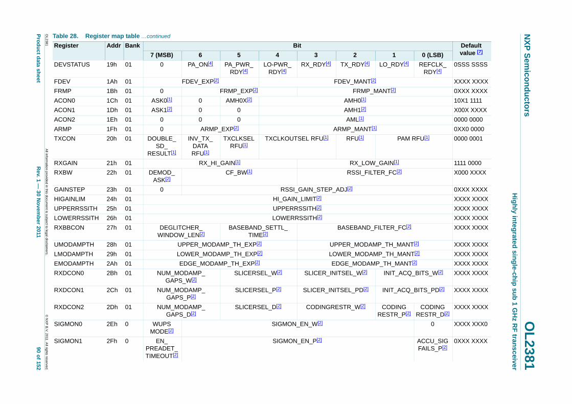
xxxxxxxxxxxxxxxxxxxxx xxxxxxxxxxxxxxxxxxxxxxxxxx xxxxxxx x x x xxxxxxxxxxxxxxxxxxxxxxxxxxxxxx xxxxxxxxxxxxxxxxxxx xx xx xxxxx xxxxxxxxxxxxxxxxxxxxxxxxxxx xxxxxxxxxxxxxxxxxxx xxxxxx xxxxxxxxxxxxxxxxxxxxxxxxxxxxxxxxxxx xxxxxxxxxxxx x x xxxxxxxxxxxxxxxxxxxxx xxxxxxxxxxxxxxxxxxxxxxxxxxxxxx xxxxx xxxxxxxxxxxxxxxxxxxxxxxxxxxxxxxxxxxxxxxxxxxxxxxxxx xxxxxxxx xxxxxxxxxxxxxxxxxxxxxxxxx xxxxxxxxxxxxxxxxxxxx xxx
OL2
381
Pro
du
ct data sh
NX
P S
emico
nd
ucto
rsO
L2381
Hig
hly
integ
rate
d sin
gle-ch
ip su
b 1
GH
z RF
tran
sc
eiver
DEVSTATUS 19h 01 0 PA_ON[4] PA_PWR_RDY[4]
LO-PWR_RDY[4]
RX_RDY[4] TX_RDY[4] LO_RDY[4] REFCLK_RDY[4]
0SSS SSSS
XXXX XXXX
ANT[2] 0XXX XXXX
10X1 1111
X00X XXXX
0000 0000
0XX0 0000
PAM RFU[1] 0000 0001
GAIN[1] 1111 0000
R_FC[2] X000 XXXX
0XXX XXXX
XXXX XXXX
XXXX XXXX
XXXX XXXX
ILTER_FC[2] XXXX XXXX
P_TH_MANT[2] XXXX XXXX
P_TH_MANT[2] XXXX XXXX
_TH_MANT[2] XXXX XXXX
INIT_ACQ_BITS_W[2] XXXX XXXX
INIT_ACQ_BITS_PD[2] XXXX XXXX
CODINGRESTR_P[2]
CODINGRESTR_D[2]
XXXX XXXX
0 XXXX XXX0
ACCU_SIGFAILS_P[2]
0XXX XXXX
Table 28. Register map table …continued
Register Addr Bank Bit Default value [7]
7 (MSB) 6 5 4 3 2 1 0 (LSB)
All inform
ation provided in this docum
ent is subject to legal disclaim
ers.©
NX
P B
.V. 20
11. All rights reserved
.
eetR
ev. 1 — 30 N
ovem
ber 2011
90 of 15
2
FDEV 1Ah 01 FDEV_EXP[2] FDEV_MANT[2]
FRMP 1Bh 01 0 FRMP_EXP[2] FRMP_M
ACON0 1Ch 01 ASK0[1] 0 AMH0X[2] AMH0[1]
ACON1 1Dh 01 ASK1[2] 0 0 AMH1[2]
ACON2 1Eh 01 0 0 0 AML[1]
ARMP 1Fh 01 0 ARMP_EXP[2] ARMP_MANT[1]
TXCON 20h 01 DOUBLE_SD_
RESULT[1]
INV_TX_DATA RFU[1]
TXCLKSEL RFU[1]
TXCLKOUTSEL RFU[1] RFU[1]
RXGAIN 21h 01 RX_HI_GAIN[1] RX_LOW_
RXBW 22h 01 DEMOD_ASK[2]
CF_BW[1] RSSI_FILTE
GAINSTEP 23h 01 0 RSSI_GAIN_STEP_ADJ[2]
HIGAINLIM 24h 01 HI_GAIN_LIMIT[2]
UPPERRSSITH 25h 01 UPPERRSSITH[2]
LOWERRSSITH 26h 01 LOWERRSSITH[2]
RXBBCON 27h 01 DEGLITCHER_WINDOW_LEN[2]
BASEBAND_SETTL_TIME[2]
BASEBAND_F
UMODAMPTH 28h 01 UPPER_MODAMP_TH_EXP[2] UPPER_MODAM
LMODAMPTH 29h 01 LOWER_MODAMP_TH_EXP[2] LOWER_MODAM
EMODAMPTH 2Ah 01 EDGE_MODAMP_TH_EXP[2] EDGE_MODAMP
RXDCON0 2Bh 01 NUM_MODAMP_GAPS_W[2]
SLICERSEL_W[2] SLICER_INITSEL_W[2]
RXDCON1 2Ch 01 NUM_MODAMP_GAPS_P[2]
SLICERSEL_P[2] SLICER_INITSEL_PD[2]
RXDCON2 2Dh 01 NUM_MODAMP_GAPS_D[2]
SLICERSEL_D[2] CODINGRESTR_W[2]
SIGMON0 2Eh 0 WUPSMODE[2]
SIGMON_EN_W[2]
SIGMON1 2Fh 0 EN_PREADET_TIMEOUT[2]
SIGMON_EN_P[2]
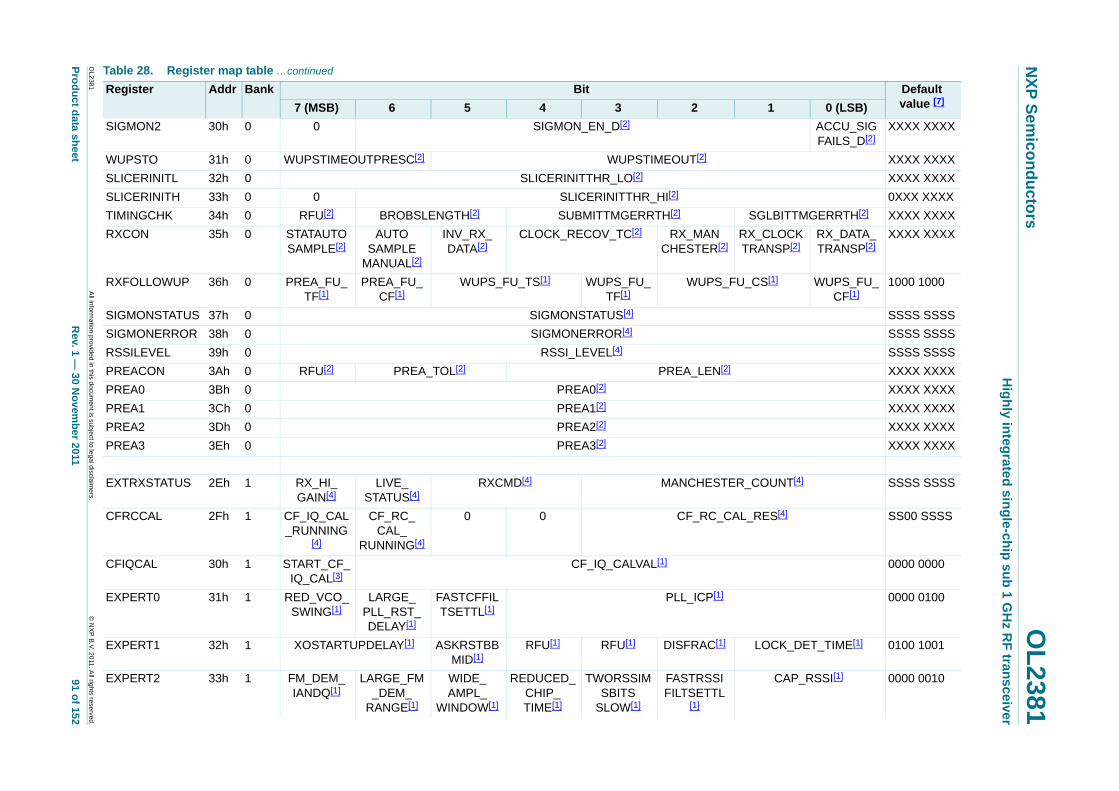
xxxxxxxxxxxxxxxxxxxxx xxxxxxxxxxxxxxxxxxxxxxxxxx xxxxxxx x x x xxxxxxxxxxxxxxxxxxxxxxxxxxxxxx xxxxxxxxxxxxxxxxxxx xx xx xxxxx xxxxxxxxxxxxxxxxxxxxxxxxxxx xxxxxxxxxxxxxxxxxxx xxxxxx xxxxxxxxxxxxxxxxxxxxxxxxxxxxxxxxxxx xxxxxxxxxxxx x x xxxxxxxxxxxxxxxxxxxxx xxxxxxxxxxxxxxxxxxxxxxxxxxxxxx xxxxx xxxxxxxxxxxxxxxxxxxxxxxxxxxxxxxxxxxxxxxxxxxxxxxxxx xxxxxxxx xxxxxxxxxxxxxxxxxxxxxxxxx xxxxxxxxxxxxxxxxxxxx xxx
OL2
381
Pro
du
ct data sh
NX
P S
emico
nd
ucto
rsO
L2381
Hig
hly
integ
rate
d sin
gle-ch
ip su
b 1
GH
z RF
tran
sc
eiver
SIGMON2 30h 0 0 SIGMON_EN_D[2] ACCU_SIGFAILS_D[2]
XXXX XXXX
XXXX XXXX
XXXX XXXX
0XXX XXXX
SGLBITTMGERRTH[2] XXXX XXXX
RX_CLOCKTRANSP[2]
RX_DATA_TRANSP[2]
XXXX XXXX
_CS[1] WUPS_FU_CF[1]
1000 1000
SSSS SSSS
SSSS SSSS
SSSS SSSS
XXXX XXXX
XXXX XXXX
XXXX XXXX
XXXX XXXX
XXXX XXXX
_COUNT[4] SSSS SSSS
L_RES[4] SS00 SSSS
0000 0000
0000 0100
LOCK_DET_TIME[1] 0100 1001
CAP_RSSI[1] 0000 0010
Table 28. Register map table …continued
Register Addr Bank Bit Default value [7]
7 (MSB) 6 5 4 3 2 1 0 (LSB)
All inform
ation provided in this docum
ent is subject to legal disclaim
ers.©
NX
P B
.V. 20
11. All rights reserved
.
eetR
ev. 1 — 30 N
ovem
ber 2011
91 of 15
2
WUPSTO 31h 0 WUPSTIMEOUTPRESC[2] WUPSTIMEOUT[2]
SLICERINITL 32h 0 SLICERINITTHR_LO[2]
SLICERINITH 33h 0 0 SLICERINITTHR_HI[2]
TIMINGCHK 34h 0 RFU[2] BROBSLENGTH[2] SUBMITTMGERRTH[2]
RXCON 35h 0 STATAUTOSAMPLE[2]
AUTOSAMPLE
MANUAL[2]
INV_RX_DATA[2]
CLOCK_RECOV_TC[2] RX_MANCHESTER[2]
RXFOLLOWUP 36h 0 PREA_FU_TF[1]
PREA_FU_CF[1]
WUPS_FU_TS[1] WUPS_FU_TF[1]
WUPS_FU
SIGMONSTATUS 37h 0 SIGMONSTATUS[4]
SIGMONERROR 38h 0 SIGMONERROR[4]
RSSILEVEL 39h 0 RSSI_LEVEL[4]
PREACON 3Ah 0 RFU[2] PREA_TOL[2] PREA_LEN[2]
PREA0 3Bh 0 PREA0[2]
PREA1 3Ch 0 PREA1[2]
PREA2 3Dh 0 PREA2[2]
PREA3 3Eh 0 PREA3[2]
EXTRXSTATUS 2Eh 1 RX_HI_GAIN[4]
LIVE_STATUS[4]
RXCMD[4] MANCHESTER
CFRCCAL 2Fh 1 CF_IQ_CAL_RUNNING
[4]
CF_RC_CAL_
RUNNING[4]
0 0 CF_RC_CA
CFIQCAL 30h 1 START_CF_IQ_CAL[3]
CF_IQ_CALVAL[1]
EXPERT0 31h 1 RED_VCO_SWING[1]
LARGE_PLL_RST_DELAY[1]
FASTCFFILTSETTL[1]
PLL_ICP[1]
EXPERT1 32h 1 XOSTARTUPDELAY[1] ASKRSTBBMID[1]
RFU[1] RFU[1] DISFRAC[1]
EXPERT2 33h 1 FM_DEM_IANDQ[1]
LARGE_FM_DEM_
RANGE[1]
WIDE_AMPL_
WINDOW[1]
REDUCED_ CHIP_TIME[1]
TWORSSIMSBITS
SLOW[1]
FASTRSSIFILTSETTL
[1]

xxxxxxxxxxxxxxxxxxxxx xxxxxxxxxxxxxxxxxxxxxxxxxx xxxxxxx x x x xxxxxxxxxxxxxxxxxxxxxxxxxxxxxx xxxxxxxxxxxxxxxxxxx xx xx xxxxx xxxxxxxxxxxxxxxxxxxxxxxxxxx xxxxxxxxxxxxxxxxxxx xxxxxx xxxxxxxxxxxxxxxxxxxxxxxxxxxxxxxxxxx xxxxxxxxxxxx x x xxxxxxxxxxxxxxxxxxxxx xxxxxxxxxxxxxxxxxxxxxxxxxxxxxx xxxxx xxxxxxxxxxxxxxxxxxxxxxxxxxxxxxxxxxxxxxxxxxxxxxxxxx xxxxxxxx xxxxxxxxxxxxxxxxxxxxxxxxx xxxxxxxxxxxxxxxxxxxx xxx
OL2
381
Pro
du
ct data sh
NX
P S
emico
nd
ucto
rsO
L2381
Hig
hly
integ
rate
d sin
gle-ch
ip su
b 1
GH
z RF
tran
sc
eiver
ice status after a reset.
EXPERT3 34h 1 0 0 0 0 RFU[1] ALLOWREGSWITCH[6]
LTDIQPHASECAL
[1]
DONOTDISTURBPTCAP[1]
0000 0000
_SEL[6] 0110 0000
RL[6] VCO_TESTON[6]
0000 0000
FORCE_LOCK_
DETECTED[5]
FORCE_XO_RDY[1]
0000 0000
RX_ON[6] PA_STEP_TEST[6]
0000 0000
_CALVAL[2] 0000 XXXX
XO_DET_DIS[6]
XO_BIAS_DIS[6]
XXXX 0000
0000 0000
0000 0000
ASYNCSCAN[1]
SCANEN[1] 0000 0000
0000 0000
0 BANK_SEL[5]
0000 0000
Table 28. Register map table …continued
Register Addr Bank Bit Default value [7]
7 (MSB) 6 5 4 3 2 1 0 (LSB)
All inform
ation provided in this docum
ent is subject to legal disclaim
ers.©
NX
P B
.V. 20
11. All rights reserved
.
eetR
ev. 1 — 30 N
ovem
ber 2011
92 of 15
2
[1] Bits/field preset at power-on.
[2] Bits cannot be preset.
[3] Command bits.
[4] Status bit (Read only) and indicated by ‘S’in the Default value column. Their values are undefined because they depend on the dev
[5] Bits/field reset in power-down mode.
[6] Test bits.
[7] ‘X’ denotes the bit is undefined after a device reset; the value is completely random and independent of the device status.
TEST0 35h 1 CF_MULTITONE_EN[6]
DIG_TEST_SEL[6] RXD_DBG
TEST1 36h 1 IQ_TEST_LV[6]
ANA_TEST_SEL[6] REG_DIG_DIS[6]
PLL_CT
TEST2 37h 1 REG_VCO_ON[6]
REG_PLL_ON[6]
REG_PA_ON[6]
FORCE_REG_VCO_
RDY[5]
FORCE_REG_PLL_
RDY[5]
FORCE_REG_PA_
RDY[5]
TEST3 38h 1 VCO_ON[6] PRESC_ON[6]
PFD_ON[6] CLK_PLL_ON[6]
TX_ON[6] RX_GAP_ON[6]
TEST4 39h 1 FORCE_CF_RC_CAL[3]
SKIP_CF_RC_CAL[6]
CF_RC_ADJUSTCAL[6] MAN_CF_RC
TEST5 3Ah 1 XO_IOFFS[2] XO_IOFFSSINK_EN
[2]
XO_IOFFSEN[6]
XO_KICK_DIS[6]
RFU 3Bh 1 -[1]
TCBEN0 3Ch 1 -[3]
TCBR 3Dh 1 - IDDQ1[1] IDDQ0[1]
TCBEN1 3Eh 1 -[3]
BANKSEL 3Fh 01 0 0 0 0 0 0
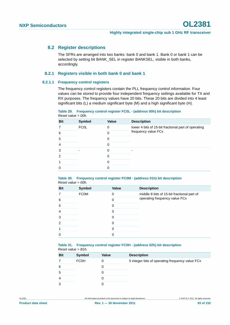
NXP Semiconductors OL2381Highly integrated single-chip sub 1 GHz RF transceiver
8.2 Register descriptions
The SFRs are arranged into two banks: bank 0 and bank 1. Bank 0 or bank 1 can be selected by setting bit BANK_SEL in register BANKSEL, visible in both banks, accordingly.
8.2.1 Registers visible in both bank 0 and bank 1
8.2.1.1 Frequency control registers
The frequency control registers contain the PLL frequency control information. Four values can be stored to provide four independent frequency settings available for TX and RX purposes. The frequency values have 20 bits. These 20 bits are divided into 4 least significant bits (L) a medium significant byte (M) and a high significant byte (H).
Table 29. Frequency control register FC0L - (address 00h) bit descriptionReset value = 00h.
Bit Symbol Value Description
7 FC0L 0 lower 4 bits of 15-bit fractional part of operating frequency value FCx6 0
5 0
4 0
3 - 0 -
2 0
1 0
0 0
Table 30. Frequency control register FC0M - (address 01h) bit descriptionReset value = 00h.
Bit Symbol Value Description
7 FC0M 0 middle 8 bits of 15-bit fractional part of operating frequency value FCx6 0
5 0
4 0
3 0
2 0
1 0
0 0
Table 31. Frequency control register FC0H - (address 02h) bit descriptionReset value = B1h.
Bit Symbol Value Description
7 FC0H 0 5 integer bits of operating frequency value FCx
6 0
5 0
4 0
3 0
OL2381 All information provided in this document is subject to legal disclaimers. © NXP B.V. 2011. All rights reserved.
Product data sheet Rev. 1 — 30 November 2011 93 of 152
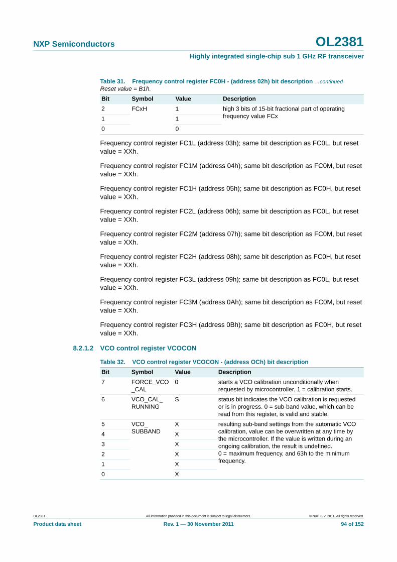
NXP Semiconductors OL2381Highly integrated single-chip sub 1 GHz RF transceiver
Frequency control register FC1L (address 03h); same bit description as FC0L, but reset value = XXh.
Frequency control register FC1M (address 04h); same bit description as FC0M, but reset value = XXh.
Frequency control register FC1H (address 05h); same bit description as FC0H, but reset value = XXh.
Frequency control register FC2L (address 06h); same bit description as FC0L, but reset value = XXh.
Frequency control register FC2M (address 07h); same bit description as FC0M, but reset value = XXh.
Frequency control register FC2H (address 08h); same bit description as FC0H, but reset value = XXh.
Frequency control register FC3L (address 09h); same bit description as FC0L, but reset value = XXh.
Frequency control register FC3M (address 0Ah); same bit description as FC0M, but reset value = XXh.
Frequency control register FC3H (address 0Bh); same bit description as FC0H, but reset value = XXh.
8.2.1.2 VCO control register VCOCON
2 FCxH 1 high 3 bits of 15-bit fractional part of operating frequency value FCx1 1
0 0
Table 31. Frequency control register FC0H - (address 02h) bit description …continuedReset value = B1h.
Bit Symbol Value Description
Table 32. VCO control register VCOCON - (address OCh) bit description
Bit Symbol Value Description
7 FORCE_VCO_CAL
0 starts a VCO calibration unconditionally when requested by microcontroller. 1 = calibration starts.
6 VCO_CAL_RUNNING
S status bit indicates the VCO calibration is requested or is in progress. 0 = sub-band value, which can be read from this register, is valid and stable.
5 VCO_SUBBAND
X resulting sub-band settings from the automatic VCO calibration, value can be overwritten at any time by the microcontroller. If the value is written during an ongoing calibration, the result is undefined. 0 = maximum frequency, and 63h to the minimum frequency.
4 X
3 X
2 X
1 X
0 X
OL2381 All information provided in this document is subject to legal disclaimers. © NXP B.V. 2011. All rights reserved.
Product data sheet Rev. 1 — 30 November 2011 94 of 152

NXP Semiconductors OL2381Highly integrated single-chip sub 1 GHz RF transceiver
8.2.1.3 Local oscillator control register LOCON
8.2.1.4 Timing register TIMING0
Register TIMING0 (address OEh), MAINSCL[6:0]: main scaler lower byte of baud-rate generator; see Table 34 for description.
8.2.1.5 Timing register TIMING1
Table 33. Local oscillator control register LOCON - (address ODh) bit description
Bit Symbol Value Description
7 CLK2SCLK_DELAY 0 delay from the 9th SCLK edge in a TX/RX command until the device starts driving the SCLK line. Only applicable if bit SEP_TX_LINES is logic 0 when sending a TX command, or bit SEP_RX_OUT is logic 0 when sending an RX command.
6 0
5 0
4 0
3 SKIP_VCO_CAL 0 automatic VCO calibration performed under the following circumstances:
• if the active FCxH, VCO_BAND, RF_LO_DIV, DOUBLE_SD_RESULT, DISFRAC changes
• if the device mode switches from/to RX mode
• if frequency selection flags A, B change
• if the PLL is started from idle mode
calibration under the first three conditions can be suppressed by setting this bit. Calibration is always executed on the last condition: PLL start up.
2 LOCK_DET_ON 0 1 = lock detector continuously monitors the PLL during operation. When logic 0, the lock detector only monitors the PLL for a short time after VCO calibration.
1 VCO_BAND 0 must be set to 1 for RF frequency bands below 400 MHz. Must be set to logic 0 for all other bands.
0 RF_LO_DIV 1 0 = VCO frequency is divided by 2 to achieve TX and RX frequency above 500 MHz. 1 = VCO frequency is divided by 4 to achieve TX and RX frequency below 500 MHz.
Table 34. Timing register TIMING1 - (address 0Fh) bit description
Bit Symbol Value Description
7 WATCHDOG_TIME
0 programmable watchdog timeout:
6 1
5 PRESC 1 baud-rate prescaler setting
generator. Baud rate is calculated:
where
CLKREF = 16 MHz, PRESC is an exponent in the
range 0 to 7 and 211 + MAINSC is the mantissa in the range 2048 to 4095. The resulting baud-rate clock can jitter by one prescaler clock cycle CLKPSC.
4 0
3 0
watchdog timeout2
15+WATCHDOG_TIME
CLKref---------------------------------------------------=
baud rateCLKref
2PRESC
------------------ 211
MAINSC+
212
------------------------------------- 1128---------=
OL2381 All information provided in this document is subject to legal disclaimers. © NXP B.V. 2011. All rights reserved.
Product data sheet Rev. 1 — 30 November 2011 95 of 152
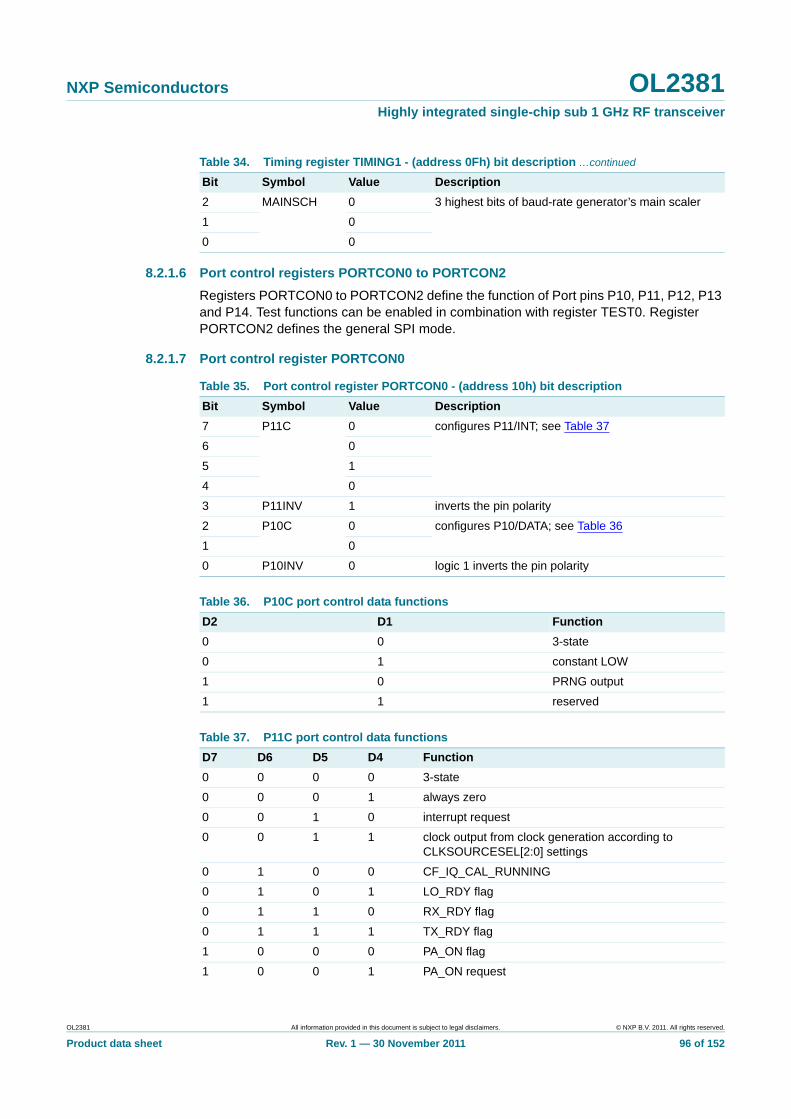
NXP Semiconductors OL2381Highly integrated single-chip sub 1 GHz RF transceiver
8.2.1.6 Port control registers PORTCON0 to PORTCON2
Registers PORTCON0 to PORTCON2 define the function of Port pins P10, P11, P12, P13 and P14. Test functions can be enabled in combination with register TEST0. Register PORTCON2 defines the general SPI mode.
8.2.1.7 Port control register PORTCON0
2 MAINSCH 0 3 highest bits of baud-rate generator’s main scaler
1 0
0 0
Table 34. Timing register TIMING1 - (address 0Fh) bit description …continued
Bit Symbol Value Description
Table 35. Port control register PORTCON0 - (address 10h) bit description
Bit Symbol Value Description
7 P11C 0 configures P11/INT; see Table 37
6 0
5 1
4 0
3 P11INV 1 inverts the pin polarity
2 P10C 0 configures P10/DATA; see Table 36
1 0
0 P10INV 0 logic 1 inverts the pin polarity
Table 36. P10C port control data functions
D2 D1 Function
0 0 3-state
0 1 constant LOW
1 0 PRNG output
1 1 reserved
Table 37. P11C port control data functions
D7 D6 D5 D4 Function
0 0 0 0 3-state
0 0 0 1 always zero
0 0 1 0 interrupt request
0 0 1 1 clock output from clock generation according to CLKSOURCESEL[2:0] settings
0 1 0 0 CF_IQ_CAL_RUNNING
0 1 0 1 LO_RDY flag
0 1 1 0 RX_RDY flag
0 1 1 1 TX_RDY flag
1 0 0 0 PA_ON flag
1 0 0 1 PA_ON request
OL2381 All information provided in this document is subject to legal disclaimers. © NXP B.V. 2011. All rights reserved.
Product data sheet Rev. 1 — 30 November 2011 96 of 152
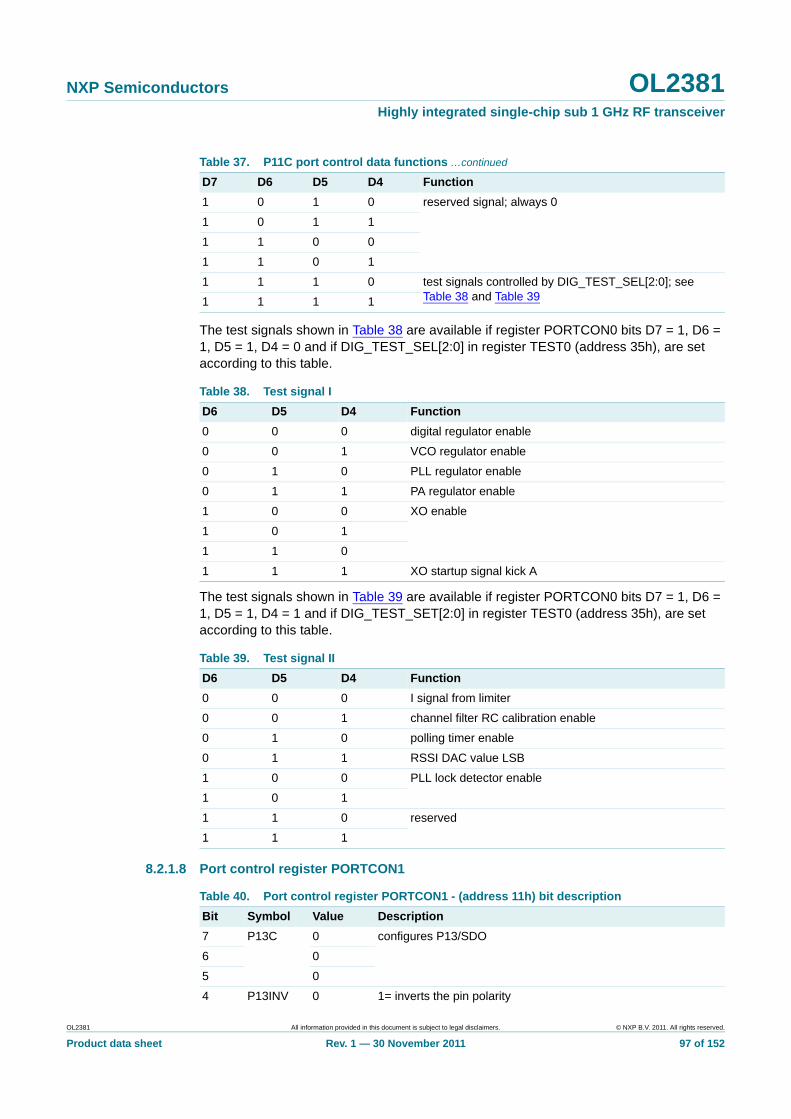
NXP Semiconductors OL2381Highly integrated single-chip sub 1 GHz RF transceiver
The test signals shown in Table 38 are available if register PORTCON0 bits D7 = 1, D6 = 1, D5 = 1, D4 = 0 and if DIG_TEST_SEL[2:0] in register TEST0 (address 35h), are set according to this table.
The test signals shown in Table 39 are available if register PORTCON0 bits D7 = 1, D6 = 1, D5 = 1, D4 = 1 and if DIG_TEST_SET[2:0] in register TEST0 (address 35h), are set according to this table.
8.2.1.8 Port control register PORTCON1
1 0 1 0 reserved signal; always 0
1 0 1 1
1 1 0 0
1 1 0 1
1 1 1 0 test signals controlled by DIG_TEST_SEL[2:0]; see Table 38 and Table 391 1 1 1
Table 38. Test signal I
D6 D5 D4 Function
0 0 0 digital regulator enable
0 0 1 VCO regulator enable
0 1 0 PLL regulator enable
0 1 1 PA regulator enable
1 0 0 XO enable
1 0 1
1 1 0
1 1 1 XO startup signal kick A
Table 39. Test signal II
D6 D5 D4 Function
0 0 0 I signal from limiter
0 0 1 channel filter RC calibration enable
0 1 0 polling timer enable
0 1 1 RSSI DAC value LSB
1 0 0 PLL lock detector enable
1 0 1
1 1 0 reserved
1 1 1
Table 37. P11C port control data functions …continued
D7 D6 D5 D4 Function
Table 40. Port control register PORTCON1 - (address 11h) bit description
Bit Symbol Value Description
7 P13C 0 configures P13/SDO
6 0
5 0
4 P13INV 0 1= inverts the pin polarity
OL2381 All information provided in this document is subject to legal disclaimers. © NXP B.V. 2011. All rights reserved.
Product data sheet Rev. 1 — 30 November 2011 97 of 152
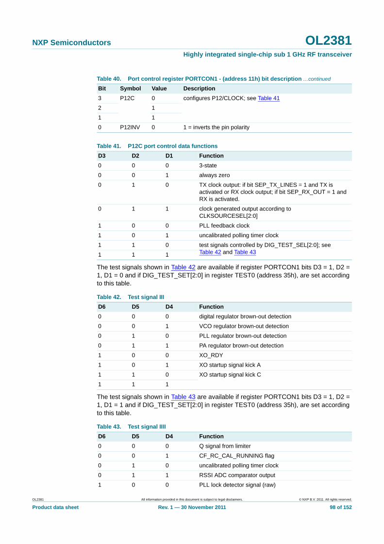
NXP Semiconductors OL2381Highly integrated single-chip sub 1 GHz RF transceiver
The test signals shown in Table 42 are available if register PORTCON1 bits D3 = 1, D2 = 1, D1 = 0 and if DIG_TEST_SET[2:0] in register TEST0 (address 35h), are set according to this table.
The test signals shown in Table 43 are available if register PORTCON1 bits D3 = 1, D2 = 1, D1 = 1 and if DIG_TEST_SET[2:0] in register TEST0 (address 35h), are set according to this table.
3 P12C 0 configures P12/CLOCK; see Table 41
2 1
1 1
0 P12INV 0 1 = inverts the pin polarity
Table 41. P12C port control data functions
D3 D2 D1 Function
0 0 0 3-state
0 0 1 always zero
0 1 0 TX clock output: if bit SEP_TX_LINES = 1 and TX is activated or RX clock output; if bit SEP_RX_OUT = 1 and RX is activated.
0 1 1 clock generated output according to CLKSOURCESEL[2:0]
1 0 0 PLL feedback clock
1 0 1 uncalibrated polling timer clock
1 1 0 test signals controlled by DIG_TEST_SEL[2:0]; see Table 42 and Table 431 1 1
Table 42. Test signal III
D6 D5 D4 Function
0 0 0 digital regulator brown-out detection
0 0 1 VCO regulator brown-out detection
0 1 0 PLL regulator brown-out detection
0 1 1 PA regulator brown-out detection
1 0 0 XO_RDY
1 0 1 XO startup signal kick A
1 1 0 XO startup signal kick C
1 1 1
Table 43. Test signal IIII
D6 D5 D4 Function
0 0 0 Q signal from limiter
0 0 1 CF_RC_CAL_RUNNING flag
0 1 0 uncalibrated polling timer clock
0 1 1 RSSI ADC comparator output
1 0 0 PLL lock detector signal (raw)
Table 40. Port control register PORTCON1 - (address 11h) bit description …continued
Bit Symbol Value Description
OL2381 All information provided in this document is subject to legal disclaimers. © NXP B.V. 2011. All rights reserved.
Product data sheet Rev. 1 — 30 November 2011 98 of 152
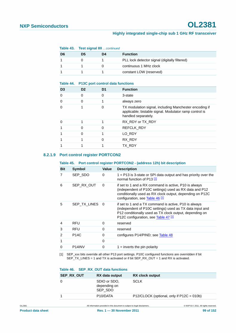
NXP Semiconductors OL2381Highly integrated single-chip sub 1 GHz RF transceiver
8.2.1.9 Port control register PORTCON2
[1] SEP_xxx bits override all other P13 port settings. P10C configured functions are overridden if bit SEP_TX_LINES = 1 and TX is activated or if bit SEP_RX_OUT = 1 and RX is activated.
1 0 1 PLL lock detector signal (digitally filtered)
1 1 0 continuous 1 MHz clock
1 1 1 constant LOW (reserved)
Table 44. P13C port control data functions
D3 D2 D1 Function
0 0 0 3-state
0 0 1 always zero
0 1 0 TX modulation signal, including Manchester encoding if applicable; bistable signal. Modulator ramp control is handled separately.
0 1 1 RX_RDY or TX_RDY
1 0 0 REFCLK_RDY
1 0 1 LO_RDY
1 1 0 RX_RDY
1 1 1 TX_RDY
Table 43. Test signal IIII …continued
D6 D5 D4 Function
Table 45. Port control register PORTCON2 - (address 12h) bit description
Bit Symbol Value Description
7 SEP_SDO 0 1 = P13 is 3-state or SPI data output and has priority over the normal function of P13 [1]
6 SEP_RX_OUT 0 if set to 1 and a RX command is active, P10 is always (independent of P10C settings) used as RX data and P12 conditionally used as RX clock output, depending on P12C configuration, see Table 46 [1]
5 SEP_TX_LINES 0 if set to 1 and a TX command is active, P10 is always (independent of P10C settings) used as TX data input and P12 conditionally used as TX clock output, depending on P12C configuration, see Table 47 [1]
4 RFU 0 reserved
3 RFU 0 reserved
2 P14C 0 configures P14/PIND; see Table 48
1 0
0 P14INV 0 1 = inverts the pin polarity
Table 46. SEP_RX_OUT data functions
SEP_RX_OUT RX data output RX clock output
0 SDIO or SDO, depending on SEP_SDO
SCLK
1 P10/DATA P12/CLOCK (optional, only if P12C = 010b)
OL2381 All information provided in this document is subject to legal disclaimers. © NXP B.V. 2011. All rights reserved.
Product data sheet Rev. 1 — 30 November 2011 99 of 152

NXP Semiconductors OL2381Highly integrated single-chip sub 1 GHz RF transceiver
8.2.1.10 General power mode register PWRMODE
[1] Bit PD can also be set automatically at Power-on reset or setting bit RESET, watchdog timer timeout, or receive state machine request. A logic 1 cannot be read because the SPI Read command causes the OL2381 to exit Power-down mode.
Table 47. SEP_TX_LINES data functions
SEP_TX_LINES TX data input TX clock output
0 SDIO SCLK
1 P10/DATA P12/CLOCK (optional, only if P12C = 010b)
Table 48. P14C port control data functions
D2 D1 Function
0 0 3-state
0 1 constant LOW
1 0 0 = RX_MODE, 1 = TX_MODE, or 3-state
1 1 0 = RX_MODE, 1 = TX_MODE, or 3-state
Table 49. General power mode register PWRMODE - (address 13h) bit description
Bit Symbol Value Description
7 0 0 -
6 0
5 0
4 POLLTIM_EN S polling timer enable bit. Initialization occurs on every (power-on) reset. Bit POLLTIM_EN is set to the inverse of pin RSTDIS. Therefore this pin controls polling timer initial condition. 1 = polling initially disabled; see Table 50 and Table 51
3 DEV_MODE 0 device mode control bits; see Table 52
2 0
1 PD 1 power-down bit: logic 1 puts device into standby mode where it consumes much less power. All analog RX and TX circuitry and the XTAL oscillator are turned off. All dynamic digital activity is stopped except SPI and polling timer, if enabled.[1]
0 RESET 0 reset bit: logic 1puts the device into power-on state, the same state reached after powering up the device. If set logic 1 with a Write command, all other bits, simultaneously written to register PWRMODE, are ignored as the register is forced to the power-on state.
Table 50. POLLTIM_EN data functions
D4 Function
0 polling timer off and no current is drawn
1 polling timer on
OL2381 All information provided in this document is subject to legal disclaimers. © NXP B.V. 2011. All rights reserved.
Product data sheet Rev. 1 — 30 November 2011 100 of 152

NXP Semiconductors OL2381Highly integrated single-chip sub 1 GHz RF transceiver
8.2.1.11 Interrupt enable register IEN
[1] Issuing another TX or RX command will not trigger this interrupt when the device is already in TX or RX mode, respectively. An interrupt is only generated when the ready state is reached.
8.2.1.12 Interrupt flag register IFLAG
The IFLAG bits indicate if an interrupt source is triggered since this register was last read. The register bits are always set to logic 0 after being read.
Table 51. Polling timer status after master reset
Pin RSTDIS Status after master reset
LOW POLLTIM_EN = 1: polling timer is activated with the settings of register POLLWUPTIME = 255 and EXTPOLLTIMRNG = 0.
HIGH POLLTIM_EN = 0: polling timer off
Table 52. DEV_MODE[1:0] device mode control functions
D3 D2 Function
0 0 crystal oscillator or external clock buffer is enabled and after crystal oscillator stabilization (if selected) the device is supplied with the reference clock
0 1 PLL controlled local oscillator (LO) enabled. LO power-up procedure includes VCO sub-band calibration (unconditionally) and PLL lock-in detection
1 0 prepare and enable RX operation. LO enabled and after PLL acquires lock, RX is switched on and enabled
1 1 prepare and enable TX operation. LO enabled and after PLL acquires lock, TX path and PA regulator are switched on and enabled. Although PA is effectively on, power control is held at zero, resulting in PA RF leakage of approximately 30 dBm RF output.
Table 53. Interrupt enable register IEN - (address 14h) bit description
Bit Symbol Value Description
7 IE_TXRX_RDY 0 triggered if either RX or TX mode is successfully reached after automatic start-up sequences issued [1]
6 IE_EOF 0 EOF is generated in data reception mode if an enabled signal monitor detects an unsatisfactory RX signal condition. This is the case when data reception mode is reached either automatically after a successful preamble detection or upon receipt of a DATA RX command.
5 IE_PREA 0 triggered on every completion of a preamble detection regardless of whether it was successful or not
4 IE_WUPS 0 triggered on every completion of a wakeup search regardless of whether it was successful or not
3 IE_POLTIM 0 triggered when a polling timer event takes place
2 IE_WATCHDOG 0 triggered when a watchdog overflow takes place
1 IE_BROWNOUT 0 triggered on brown-out detection of the voltage regulators (undervoltage detection)
0 0 0 0
OL2381 All information provided in this document is subject to legal disclaimers. © NXP B.V. 2011. All rights reserved.
Product data sheet Rev. 1 — 30 November 2011 101 of 152
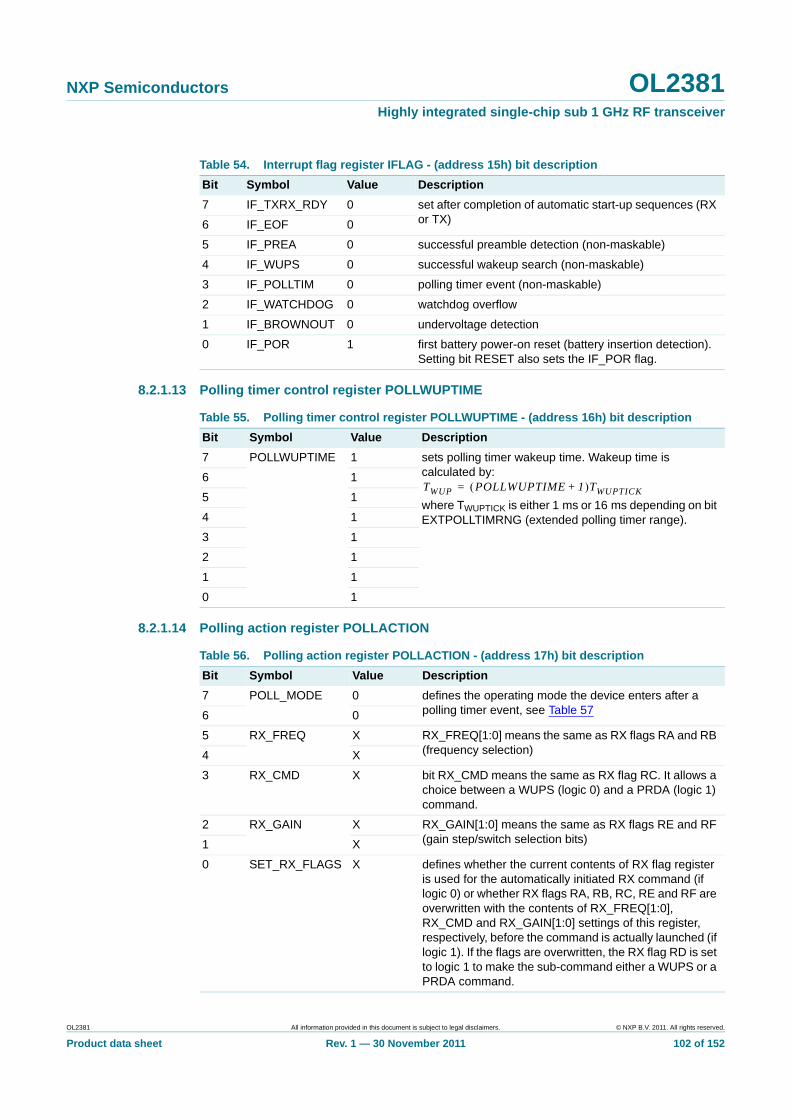
NXP Semiconductors OL2381Highly integrated single-chip sub 1 GHz RF transceiver
8.2.1.13 Polling timer control register POLLWUPTIME
8.2.1.14 Polling action register POLLACTION
Table 54. Interrupt flag register IFLAG - (address 15h) bit description
Bit Symbol Value Description
7 IF_TXRX_RDY 0 set after completion of automatic start-up sequences (RX or TX)6 IF_EOF 0
5 IF_PREA 0 successful preamble detection (non-maskable)
4 IF_WUPS 0 successful wakeup search (non-maskable)
3 IF_POLLTIM 0 polling timer event (non-maskable)
2 IF_WATCHDOG 0 watchdog overflow
1 IF_BROWNOUT 0 undervoltage detection
0 IF_POR 1 first battery power-on reset (battery insertion detection). Setting bit RESET also sets the IF_POR flag.
Table 55. Polling timer control register POLLWUPTIME - (address 16h) bit description
Bit Symbol Value Description
7 POLLWUPTIME 1 sets polling timer wakeup time. Wakeup time is calculated by:
where TWUPTICK is either 1 ms or 16 ms depending on bit EXTPOLLTIMRNG (extended polling timer range).
6 1
5 1
4 1
3 1
2 1
1 1
0 1
TWUP POLLWUPTIME 1+ TWUPTICK=
Table 56. Polling action register POLLACTION - (address 17h) bit description
Bit Symbol Value Description
7 POLL_MODE 0 defines the operating mode the device enters after a polling timer event, see Table 576 0
5 RX_FREQ X RX_FREQ[1:0] means the same as RX flags RA and RB (frequency selection)4 X
3 RX_CMD X bit RX_CMD means the same as RX flag RC. It allows a choice between a WUPS (logic 0) and a PRDA (logic 1) command.
2 RX_GAIN X RX_GAIN[1:0] means the same as RX flags RE and RF (gain step/switch selection bits)1 X
0 SET_RX_FLAGS X defines whether the current contents of RX flag register is used for the automatically initiated RX command (if logic 0) or whether RX flags RA, RB, RC, RE and RF are overwritten with the contents of RX_FREQ[1:0], RX_CMD and RX_GAIN[1:0] settings of this register, respectively, before the command is actually launched (if logic 1). If the flags are overwritten, the RX flag RD is set to logic 1 to make the sub-command either a WUPS or a PRDA command.
OL2381 All information provided in this document is subject to legal disclaimers. © NXP B.V. 2011. All rights reserved.
Product data sheet Rev. 1 — 30 November 2011 102 of 152

NXP Semiconductors OL2381Highly integrated single-chip sub 1 GHz RF transceiver
8.2.1.15 Clock connection register CLOCKCON
Table 57. POLL_MODE[1:0] device mode control functions
D7 D6 Function
0 0 after signaling the polling timer interrupt, which is unmaskable, the device remains in Power-down mode
0 1 after signaling the polling timer interrupt, which is unmaskable, the device leaves Power-down mode, which turns the crystal oscillator or the external clock buffer on
1 0 device is fully powered up to RX mode. If the polling timer interrupt is enabled, an interrupt occurs, either with the polling timer event or when the receiver is ready
1 1 device is fully powered up to RX mode. After RX settles, an RX command is automatically initiated as configured by the remaining bits of this register. It is guaranteed that at least one interrupt will occur in the command sequence.
Table 58. Clock connection register CLOCKCON - (address 18h) bit description
Bit Symbol Value Description
7 MANUALPTCAL 0 manual start of polling timer calibration. Reading bit MANUALPTCAL always yields zero. Manual calibration is only executed if polling timer and crystal oscillator are running. Otherwise the request is ignored.
6 PTCALRUNNING S status bit set when polling timer calibration is running
5 EXTPOLLTIMRNG 0 extended polling timer range calculated
by: ms; see
Table 59
4 CLKSOURCESEL 0 clock selection for selected port pin; see Table 60
3 0
2 1
1 EXT_CLK_BUF_EN 0 external clock buffer enable bit is used to turn on clock buffer for external clock. The effect of this bit also depends on bit XODIS; see Table 61
0 XODIS 0
Table 59. EXTPOLLTIMRNG bit functions
EXTPOLLTIMRNG Wakeup counter resolution TWUPTICK
Selectable wakeup times TWUP
0 1 ms 1 ms to 256 ms
1 16 ms 16 ms to 4096 ms
Table 60. CLKSOURCESEL bit functions
D4 D3 D2 Port pin
0 0 0 reference clock (16 MHz)
0 0 1 reference clock / 2 (8 MHz)
0 1 0 reference clock / 4 (4 MHz)
0 1 1 reference clock / 8 (2 MHz)
1 0 0 4 chip clock
TWUPTICK 1 15 EXTPOLLTIMRNG+=
OL2381 All information provided in this document is subject to legal disclaimers. © NXP B.V. 2011. All rights reserved.
Product data sheet Rev. 1 — 30 November 2011 103 of 152

NXP Semiconductors OL2381Highly integrated single-chip sub 1 GHz RF transceiver
8.2.1.16 Device status register DEVSTATUS
8.2.1.17 Register FDEV
Register FDEV bits set the TX FSK frequency deviation; see Section 7.20.1 “Frequency modulation” on page 42 for the calculation of the frequency deviation that is actually applied.
1 0 1 2 chip clock
1 1 0 chip clock
1 1 1 bit clock
Table 61. EXT_CLK_BUF_EN / XODIS bit functions
D1 D0 Function
0 0 crystal oscillator enabled. Digital reference clock disabled during oscillator start-up.
0 1 crystal oscillator and external clock buffer disabled
1 0 crystal oscillator enabled. Digital reference clock permanently enabled and during oscillator start-up.
1 1 crystal oscillator disabled and external clock buffer enabled. Digital reference clock permanently enabled.
Table 60. CLKSOURCESEL bit functions …continued
D4 D3 D2 Port pin
Table 62. Device status register DEVSTATUS - (address 19h) bit description
Bit Symbol Value Description
7 0 0 -
6 PA_ON 0 logic 1 indicates PA is turned on by a TX command. This remains set until ramp-down is completed (if engaged) after request is made to terminate transmission. Logic 0 indicates PA is not transmitting (although it may be supplied with power and thus emitting some RF (30 dBm) due to leakage.
5 PA_PWR_RDY 0 logic 1 indicates PA regulator is supplying power to the PA
4 LO_PWR_RDY 0 logic 1 indicates VCO and PLL regulators are delivering power to these LO sections
3 RX_RDY S status bit: automated RX mode preparation sequence ready, device ready for RX
2 TX_RDY S status bit: automated TX mode preparation sequence ready, device ready for TX
1 LO_RDY S status bit: VCO running, PLL settled and locked
0 REFCLK_RDY S status bit: XTAL oscillator stable or external clock available. External clock stability is not checked by the device.
Table 63. FSK frequency deviation register FDEV - (address 1Ah) bit description
Bit Symbol Value Description
7 FDEV_EXP X FSK frequency deviation 3-bit exponent
6 X
5 X
OL2381 All information provided in this document is subject to legal disclaimers. © NXP B.V. 2011. All rights reserved.
Product data sheet Rev. 1 — 30 November 2011 104 of 152
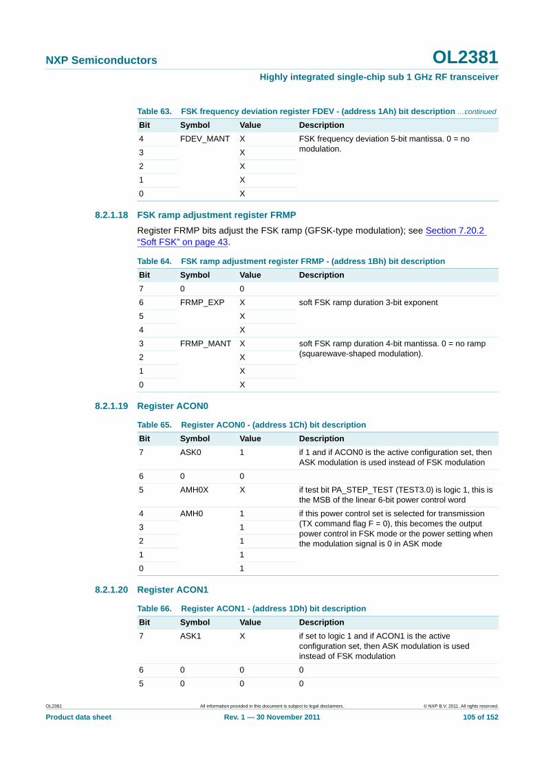
NXP Semiconductors OL2381Highly integrated single-chip sub 1 GHz RF transceiver
8.2.1.18 FSK ramp adjustment register FRMP
Register FRMP bits adjust the FSK ramp (GFSK-type modulation); see Section 7.20.2 “Soft FSK” on page 43.
8.2.1.19 Register ACON0
8.2.1.20 Register ACON1
4 FDEV_MANT X FSK frequency deviation 5-bit mantissa. 0 = no modulation.3 X
2 X
1 X
0 X
Table 63. FSK frequency deviation register FDEV - (address 1Ah) bit description …continued
Bit Symbol Value Description
Table 64. FSK ramp adjustment register FRMP - (address 1Bh) bit description
Bit Symbol Value Description
7 0 0
6 FRMP_EXP X soft FSK ramp duration 3-bit exponent
5 X
4 X
3 FRMP_MANT X soft FSK ramp duration 4-bit mantissa. 0 = no ramp (squarewave-shaped modulation).2 X
1 X
0 X
Table 65. Register ACON0 - (address 1Ch) bit description
Bit Symbol Value Description
7 ASK0 1 if 1 and if ACON0 is the active configuration set, then ASK modulation is used instead of FSK modulation
6 0 0
5 AMH0X X if test bit PA_STEP_TEST (TEST3.0) is logic 1, this is the MSB of the linear 6-bit power control word
4 AMH0 1 if this power control set is selected for transmission (TX command flag F = 0), this becomes the output power control in FSK mode or the power setting when the modulation signal is 0 in ASK mode
3 1
2 1
1 1
0 1
Table 66. Register ACON1 - (address 1Dh) bit description
Bit Symbol Value Description
7 ASK1 X if set to logic 1 and if ACON1 is the active configuration set, then ASK modulation is used instead of FSK modulation
6 0 0 0
5 0 0 0
OL2381 All information provided in this document is subject to legal disclaimers. © NXP B.V. 2011. All rights reserved.
Product data sheet Rev. 1 — 30 November 2011 105 of 152

NXP Semiconductors OL2381Highly integrated single-chip sub 1 GHz RF transceiver
8.2.1.21 Register ACON2
8.2.1.22 Register ARMP
The ARMP bits adjust the ASK ramp (soft power-on sequence); see Section 7.18 “Soft ASK, ramp control” on page 41 for more details. These settings are also applied in FSK mode to ramp the carrier up and down at the start and end of the transmission frame.
4 AMH1 X if this power control set is selected for transmission (TX command flag F = 1), this becomes the output power control in FSK mode or the power setting when the modulation signal is 0 in ASK mode
3 X
2 X
1 X
0 X
Table 66. Register ACON1 - (address 1Dh) bit description …continued
Bit Symbol Value Description
Table 67. Register ACON2 - (address 1Eh) bit description
Bit Symbol Value Description
7 0 0 -
6 0 0 -
5 0 0 -
4 AML 0 If ASK modulation is selected, this controls the output power when the modulation signal is 1.3 0
2 0
1 0
0 0
Table 68. Register ARMP - (address 1Fh) bit description
Bit Symbol Value Description
7 0 0 -
6 ARMP_EXP 0 ARMP amplitude ramp duration 2-bit exponent
5 0
4 ARMP_MANT 0 ARMP amplitude ramp duration 5-bit mantissa
3 0
2 0
1 0
0 0
OL2381 All information provided in this document is subject to legal disclaimers. © NXP B.V. 2011. All rights reserved.
Product data sheet Rev. 1 — 30 November 2011 106 of 152

NXP Semiconductors OL2381Highly integrated single-chip sub 1 GHz RF transceiver
8.2.1.23 Transmitter control register TXCON
Table 69. Transmitter control register TXCON - (address 20h) bit description
Bit Symbol Value Description
7 DOUBLE_SD_RESULT
0 configures the Sigma delta fractional-N modulation; see Section 7.14.7 “Delta-sigma modulator for fractional-N synthesis” on page 30 for details
6 INV_TX_DATA 0 logic 0 produces center frequency plus frequency deviation in FSK mode and also the power value set with AMHx in ASK mode; a logic 1 produces center frequency minus frequency deviation in FSK mode and also the power value set by AML. Setting bit INV_TX_DATA inverts this assignment. This is valid for NRZ mode and for the first bit half in Manchester mode; during the second half, the signal is inverted with respect to the first half.
5 TXCLKSEL 0 clock source for data-transmission synchronization. When logic 1, the bit clock is used as the TX clock (CLKTX = CLKBIT). If logic 0, the chip clock is used as the TX clock (CLKTX = CLKCHIP). If automatic Manchester generation is required the bit clock must be selected.
4 TXCLKOUTSEL 0 selects the clock output at port pin SCLK or P12/CLOCK
3 0
2 RFU 0 reserved
1 PAM 0 power mode selection for PA. The PA supply voltage can be selected between 3 different levels, enabling different output power ranges to be selected.
0 1
Table 70. RX frequency offset
RF_LO_DIV DOUBLE_SD_RESULT
Offset value Frequency resolution (Hz)
RX frequency offset
0 0 614 488.3 299.805 kHz
0 1 307 976.6
1 0 1228 244.1
1 1 614 488.3
Table 71. Clock output selection for the TX command, TXCLKOUTSEL
D4 D3 Selected clock at SCLK or P12/CLOCK during TX command
0 0 CLKTX
0 1 CLKTX 2
1 0 CLKTX 4
1 1 no clock selected
Table 72. PAM definition[1]
D1 D0 PA supply Output power range
0 0 1.5 V 17 dBm to 10 dBm
0 1 1.75 V 13 dBm to 11 dBm
1 0 1.95 V 11 dBm to 12 dBm
1 1 reserved -
OL2381 All information provided in this document is subject to legal disclaimers. © NXP B.V. 2011. All rights reserved.
Product data sheet Rev. 1 — 30 November 2011 107 of 152
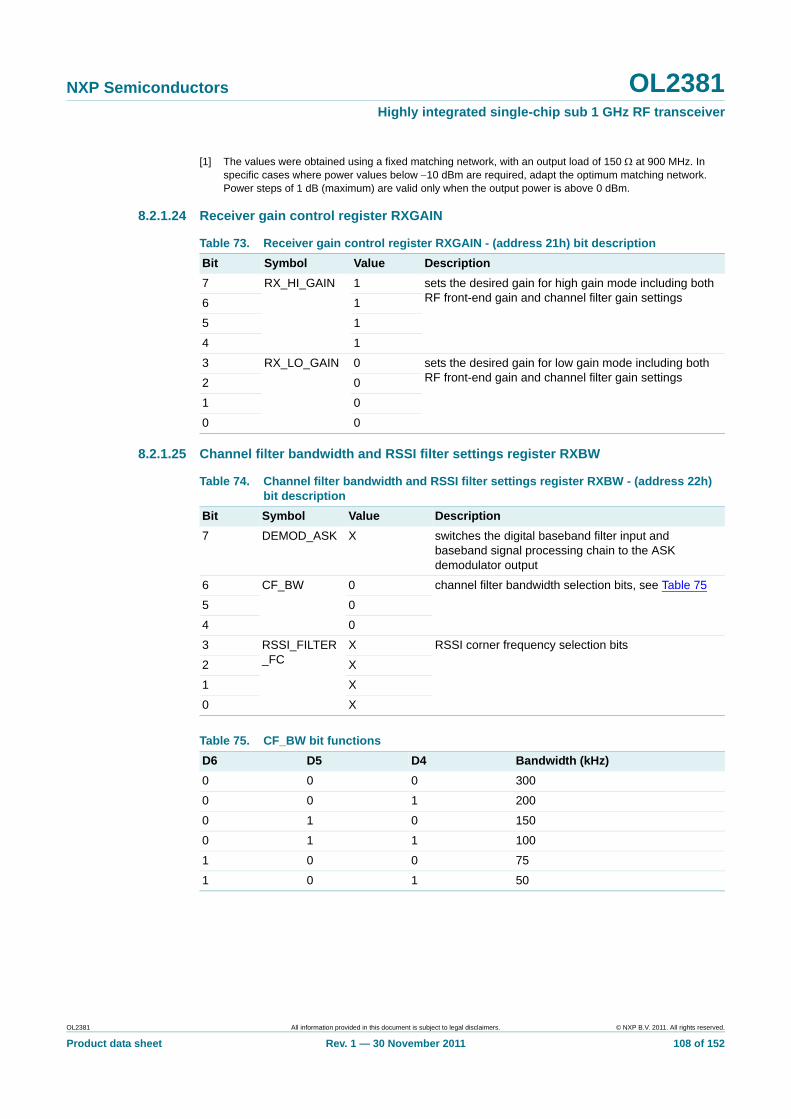
NXP Semiconductors OL2381Highly integrated single-chip sub 1 GHz RF transceiver
[1] The values were obtained using a fixed matching network, with an output load of 150 at 900 MHz. In specific cases where power values below 10 dBm are required, adapt the optimum matching network. Power steps of 1 dB (maximum) are valid only when the output power is above 0 dBm.
8.2.1.24 Receiver gain control register RXGAIN
8.2.1.25 Channel filter bandwidth and RSSI filter settings register RXBW
Table 73. Receiver gain control register RXGAIN - (address 21h) bit description
Bit Symbol Value Description
7 RX_HI_GAIN 1 sets the desired gain for high gain mode including both RF front-end gain and channel filter gain settings6 1
5 1
4 1
3 RX_LO_GAIN 0 sets the desired gain for low gain mode including both RF front-end gain and channel filter gain settings2 0
1 0
0 0
Table 74. Channel filter bandwidth and RSSI filter settings register RXBW - (address 22h) bit description
Bit Symbol Value Description
7 DEMOD_ASK X switches the digital baseband filter input and baseband signal processing chain to the ASK demodulator output
6 CF_BW 0 channel filter bandwidth selection bits, see Table 75
5 0
4 0
3 RSSI_FILTER_FC
X RSSI corner frequency selection bits
2 X
1 X
0 X
Table 75. CF_BW bit functions
D6 D5 D4 Bandwidth (kHz)
0 0 0 300
0 0 1 200
0 1 0 150
0 1 1 100
1 0 0 75
1 0 1 50
OL2381 All information provided in this document is subject to legal disclaimers. © NXP B.V. 2011. All rights reserved.
Product data sheet Rev. 1 — 30 November 2011 108 of 152
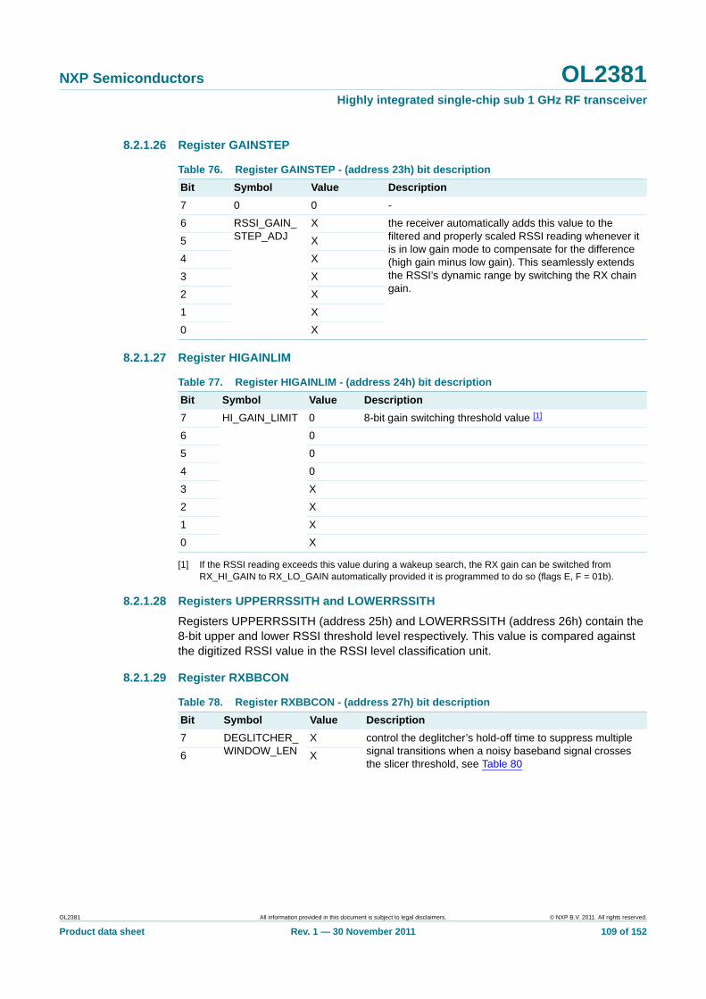
NXP Semiconductors OL2381Highly integrated single-chip sub 1 GHz RF transceiver
8.2.1.26 Register GAINSTEP
8.2.1.27 Register HIGAINLIM
[1] If the RSSI reading exceeds this value during a wakeup search, the RX gain can be switched from RX_HI_GAIN to RX_LO_GAIN automatically provided it is programmed to do so (flags E, F = 01b).
8.2.1.28 Registers UPPERRSSITH and LOWERRSSITH
Registers UPPERRSSITH (address 25h) and LOWERRSSITH (address 26h) contain the 8-bit upper and lower RSSI threshold level respectively. This value is compared against the digitized RSSI value in the RSSI level classification unit.
8.2.1.29 Register RXBBCON
Table 76. Register GAINSTEP - (address 23h) bit description
Bit Symbol Value Description
7 0 0 -
6 RSSI_GAIN_STEP_ADJ
X the receiver automatically adds this value to the filtered and properly scaled RSSI reading whenever it is in low gain mode to compensate for the difference (high gain minus low gain). This seamlessly extends the RSSI’s dynamic range by switching the RX chain gain.
5 X
4 X
3 X
2 X
1 X
0 X
Table 77. Register HIGAINLIM - (address 24h) bit description
Bit Symbol Value Description
7 HI_GAIN_LIMIT 0 8-bit gain switching threshold value [1]
6 0
5 0
4 0
3 X
2 X
1 X
0 X
Table 78. Register RXBBCON - (address 27h) bit description
Bit Symbol Value Description
7 DEGLITCHER_WINDOW_LEN
X control the deglitcher’s hold-off time to suppress multiple signal transitions when a noisy baseband signal crosses the slicer threshold, see Table 80
6 X
OL2381 All information provided in this document is subject to legal disclaimers. © NXP B.V. 2011. All rights reserved.
Product data sheet Rev. 1 — 30 November 2011 109 of 152
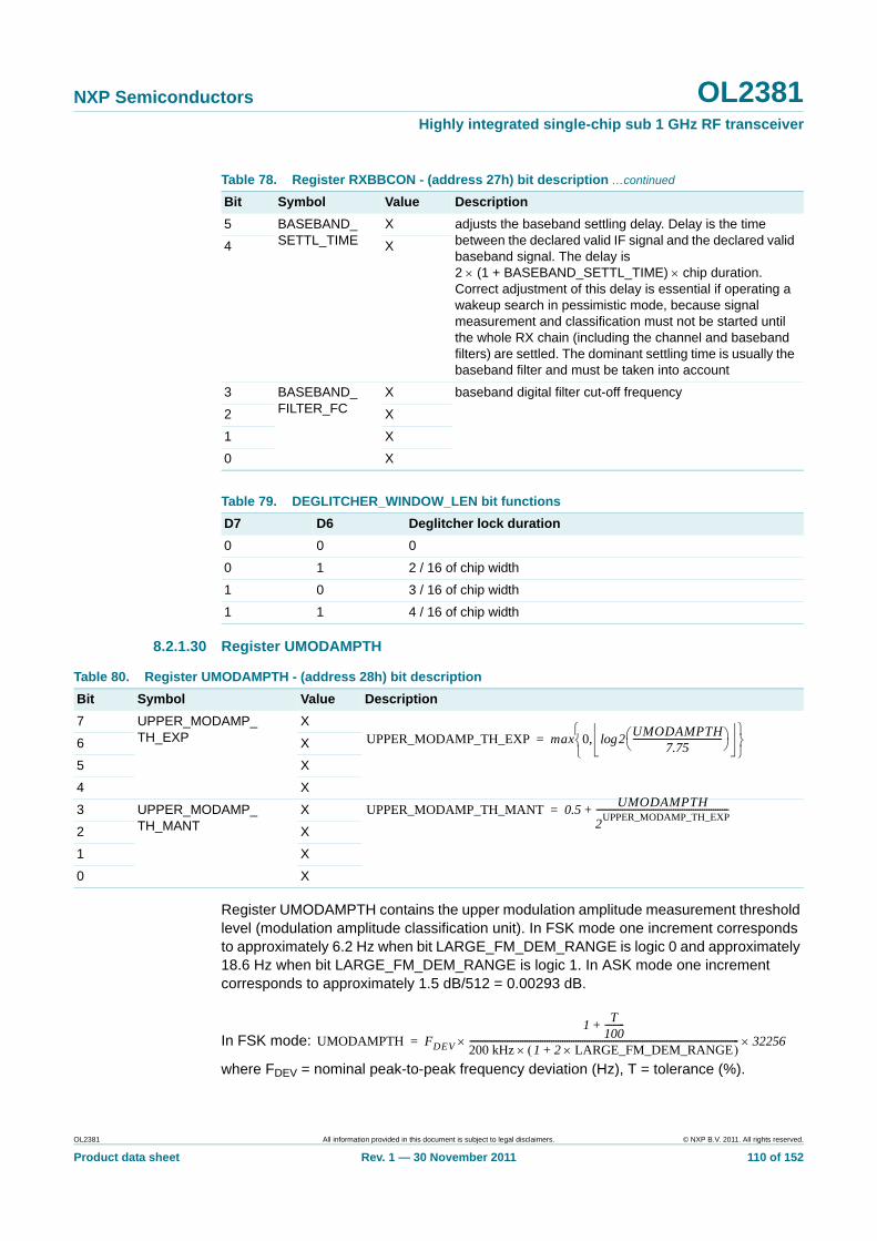
NXP Semiconductors OL2381Highly integrated single-chip sub 1 GHz RF transceiver
8.2.1.30 Register UMODAMPTH
Register UMODAMPTH contains the upper modulation amplitude measurement threshold level (modulation amplitude classification unit). In FSK mode one increment corresponds to approximately 6.2 Hz when bit LARGE_FM_DEM_RANGE is logic 0 and approximately 18.6 Hz when bit LARGE_FM_DEM_RANGE is logic 1. In ASK mode one increment corresponds to approximately 1.5 dB/512 = 0.00293 dB.
In FSK mode:
where FDEV = nominal peak-to-peak frequency deviation (Hz), T = tolerance (%).
5 BASEBAND_SETTL_TIME
X adjusts the baseband settling delay. Delay is the time between the declared valid IF signal and the declared valid baseband signal. The delay is 2 (1 + BASEBAND_SETTL_TIME) chip duration. Correct adjustment of this delay is essential if operating a wakeup search in pessimistic mode, because signal measurement and classification must not be started until the whole RX chain (including the channel and baseband filters) are settled. The dominant settling time is usually the baseband filter and must be taken into account
4 X
3 BASEBAND_FILTER_FC
X baseband digital filter cut-off frequency
2 X
1 X
0 X
Table 79. DEGLITCHER_WINDOW_LEN bit functions
D7 D6 Deglitcher lock duration
0 0 0
0 1 2 / 16 of chip width
1 0 3 / 16 of chip width
1 1 4 / 16 of chip width
Table 78. Register RXBBCON - (address 27h) bit description …continued
Bit Symbol Value Description
Table 80. Register UMODAMPTH - (address 28h) bit description
Bit Symbol Value Description
7 UPPER_MODAMP_TH_EXP
X
6 X
5 X
4 X
3 UPPER_MODAMP_TH_MANT
X
2 X
1 X
0 X
UPPER_MODAMP_TH_EXP max 0, 2UMODAMPTH
7.75---------------------------------------- log
=
UPPER_MODAMP_TH_MANT 0.5UMODAMPTH
2UPPER_MODAMP_TH_EXP
------------------------------------------------------------+=
UMODAMPTH FDEV
1T
100---------+
200 kHz 1 2 LARGE_FM_DEM_RANGE+ -------------------------------------------------------------------------------------------------------------------------- 32256=
OL2381 All information provided in this document is subject to legal disclaimers. © NXP B.V. 2011. All rights reserved.
Product data sheet Rev. 1 — 30 November 2011 110 of 152

NXP Semiconductors OL2381Highly integrated single-chip sub 1 GHz RF transceiver
In ASK mode: where ASKMOD = ASK
modulation amplitude ratio (dB), T = tolerance (%).
Remark: The specified amplitude is peak-to-peak.
8.2.1.31 Register LMODAMPTH
Register LMODAMPTH (address 29h) contains the lower modulation amplitude measurement threshold level (modulation amplitude classification unit). It configures the threshold level similar to register UMODAMPTH.
In FSK mode:
where FDEV = nominal peak-to-peak frequency deviation (Hz), T = tolerance (%).
In ASK mode: where ASKMOD = ASK
modulation amplitude ratio (dB), T = tolerance (%).
Remark: The specified amplitude is peak-to-peak.
8.2.1.32 Register EMODAMPTH
The EMODAMPTH register contains the expected peak modulation value used as the amplitude reference value for the edge slicer. It configures the threshold level similar to register UMODAMPTH.
In FSK mode:
where FDEV = nominal peak-to-peak frequency deviation (Hz).
In ASK mode: where ASKMOD = ASK modulation
amplitude ratio (dB).
Remark: The specified amplitude is peak.
UMODAMPTH ASKMOD
1T
100---------+
1.5------------------ 512=
LMODAMPTH FDEV
1T
100---------+
200 kHz 1 2 LARGE_FM_DEM_RANGE+ -------------------------------------------------------------------------------------------------------------------------- 32256=
LMODAMPTH ASKMOD
1T
100---------+
1.5------------------ 512=
Table 81. Register EMODAMPTH - (address 2Ah) bit description
Bit Symbol Value Description
7 EDGE_MODAMP_TH 0 expected peak modulation value; calculation of EDGE_MODAMP_TH ; see register UMODAMPTH
6 0
5 0
4 0
3 0
2 0
1 0
0 0
EMODAMPTH FDEV
FDEV
200 kHz 1 2 LARGE_FM_DEM_RANGE+ -------------------------------------------------------------------------------------------------------------------------- 32256=
EMODAMPTHASKMOD
3---------------------- 512=
OL2381 All information provided in this document is subject to legal disclaimers. © NXP B.V. 2011. All rights reserved.
Product data sheet Rev. 1 — 30 November 2011 111 of 152
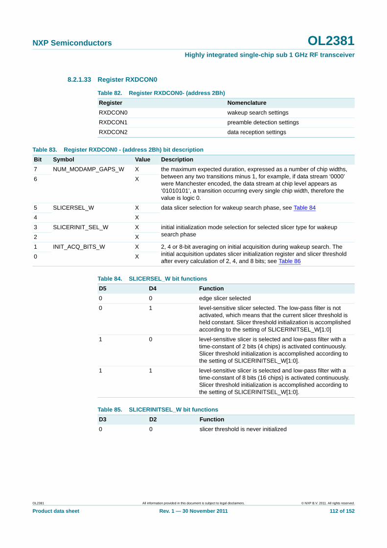
NXP Semiconductors OL2381Highly integrated single-chip sub 1 GHz RF transceiver
8.2.1.33 Register RXDCON0
Table 82. Register RXDCON0- (address 2Bh)
Register Nomenclature
RXDCON0 wakeup search settings
RXDCON1 preamble detection settings
RXDCON2 data reception settings
Table 83. Register RXDCON0 - (address 2Bh) bit description
Bit Symbol Value Description
7 NUM_MODAMP_GAPS_W X the maximum expected duration, expressed as a number of chip widths, between any two transitions minus 1, for example, if data stream ‘0000’ were Manchester encoded, the data stream at chip level appears as ‘01010101’, a transition occurring every single chip width, therefore the value is logic 0.
6 X
5 SLICERSEL_W X data slicer selection for wakeup search phase, see Table 84
4 X
3 SLICERINIT_SEL_W X initial initialization mode selection for selected slicer type for wakeup search phase2 X
1 INIT_ACQ_BITS_W X 2, 4 or 8-bit averaging on initial acquisition during wakeup search. The initial acquisition updates slicer initialization register and slicer threshold after every calculation of 2, 4, and 8 bits; see Table 86
0 X
Table 84. SLICERSEL_W bit functions
D5 D4 Function
0 0 edge slicer selected
0 1 level-sensitive slicer selected. The low-pass filter is not activated, which means that the current slicer threshold is held constant. Slicer threshold initialization is accomplished according to the setting of SLICERINITSEL_W[1:0]
1 0 level-sensitive slicer is selected and low-pass filter with a time-constant of 2 bits (4 chips) is activated continuously. Slicer threshold initialization is accomplished according to the setting of SLICERINITSEL_W[1:0].
1 1 level-sensitive slicer is selected and low-pass filter with a time-constant of 8 bits (16 chips) is activated continuously. Slicer threshold initialization is accomplished according to the setting of SLICERINITSEL_W[1:0].
Table 85. SLICERINITSEL_W bit functions
D3 D2 Function
0 0 slicer threshold is never initialized
OL2381 All information provided in this document is subject to legal disclaimers. © NXP B.V. 2011. All rights reserved.
Product data sheet Rev. 1 — 30 November 2011 112 of 152
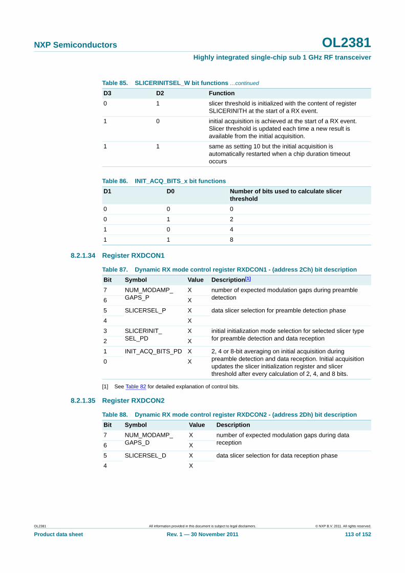
NXP Semiconductors OL2381Highly integrated single-chip sub 1 GHz RF transceiver
8.2.1.34 Register RXDCON1
[1] See Table 82 for detailed explanation of control bits.
8.2.1.35 Register RXDCON2
0 1 slicer threshold is initialized with the content of register SLICERINITH at the start of a RX event.
1 0 initial acquisition is achieved at the start of a RX event. Slicer threshold is updated each time a new result is available from the initial acquisition.
1 1 same as setting 10 but the initial acquisition is automatically restarted when a chip duration timeout occurs
Table 86. INIT_ACQ_BITS_x bit functions
D1 D0 Number of bits used to calculate slicer threshold
0 0 0
0 1 2
1 0 4
1 1 8
Table 85. SLICERINITSEL_W bit functions …continued
D3 D2 Function
Table 87. Dynamic RX mode control register RXDCON1 - (address 2Ch) bit description
Bit Symbol Value Description[1]
7 NUM_MODAMP_GAPS_P
X number of expected modulation gaps during preamble detection6 X
5 SLICERSEL_P X data slicer selection for preamble detection phase
4 X
3 SLICERINIT_SEL_PD
X initial initialization mode selection for selected slicer type for preamble detection and data reception2 X
1 INIT_ACQ_BITS_PD X 2, 4 or 8-bit averaging on initial acquisition during preamble detection and data reception. Initial acquisition updates the slicer initialization register and slicer threshold after every calculation of 2, 4, and 8 bits.
0 X
Table 88. Dynamic RX mode control register RXDCON2 - (address 2Dh) bit description
Bit Symbol Value Description
7 NUM_MODAMP_GAPS_D
X number of expected modulation gaps during data reception6 X
5 SLICERSEL_D X data slicer selection for data reception phase
4 X
OL2381 All information provided in this document is subject to legal disclaimers. © NXP B.V. 2011. All rights reserved.
Product data sheet Rev. 1 — 30 November 2011 113 of 152
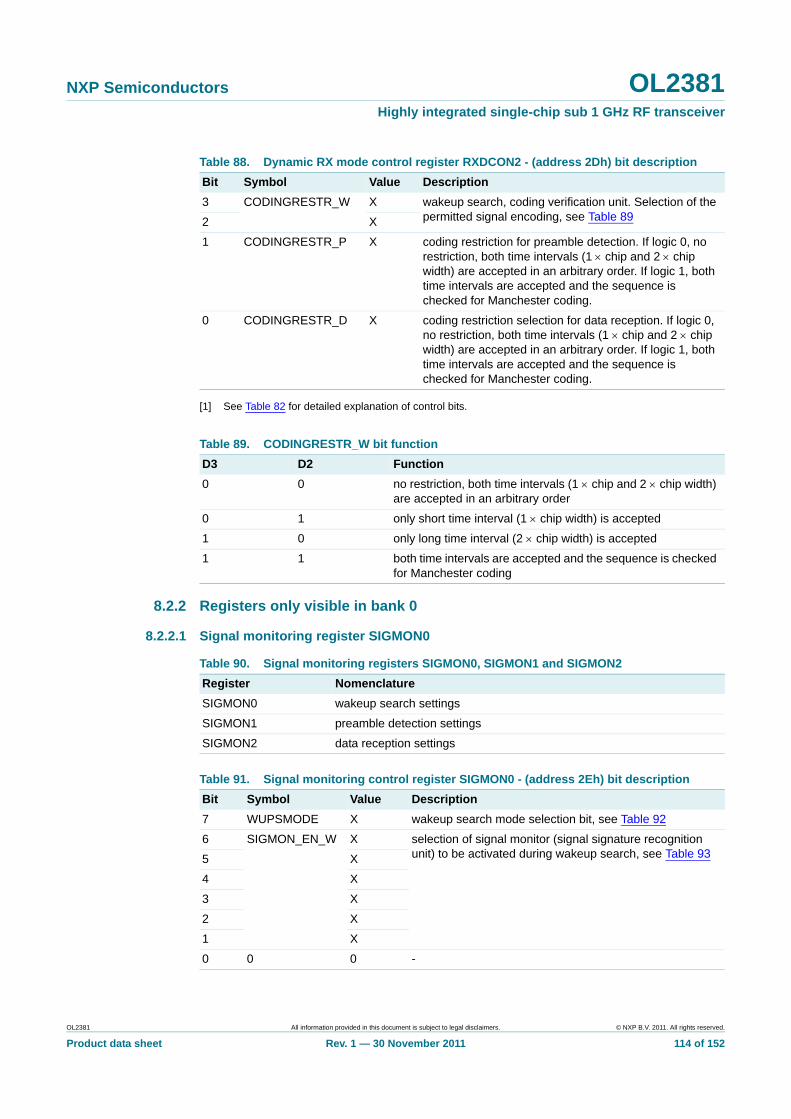
NXP Semiconductors OL2381Highly integrated single-chip sub 1 GHz RF transceiver
[1] See Table 82 for detailed explanation of control bits.
8.2.2 Registers only visible in bank 0
8.2.2.1 Signal monitoring register SIGMON0
3 CODINGRESTR_W X wakeup search, coding verification unit. Selection of the permitted signal encoding, see Table 892 X
1 CODINGRESTR_P X coding restriction for preamble detection. If logic 0, no restriction, both time intervals (1 chip and 2 chip width) are accepted in an arbitrary order. If logic 1, both time intervals are accepted and the sequence is checked for Manchester coding.
0 CODINGRESTR_D X coding restriction selection for data reception. If logic 0, no restriction, both time intervals (1 chip and 2 chip width) are accepted in an arbitrary order. If logic 1, both time intervals are accepted and the sequence is checked for Manchester coding.
Table 89. CODINGRESTR_W bit function
D3 D2 Function
0 0 no restriction, both time intervals (1 chip and 2 chip width) are accepted in an arbitrary order
0 1 only short time interval (1 chip width) is accepted
1 0 only long time interval (2 chip width) is accepted
1 1 both time intervals are accepted and the sequence is checked for Manchester coding
Table 88. Dynamic RX mode control register RXDCON2 - (address 2Dh) bit description
Bit Symbol Value Description
Table 90. Signal monitoring registers SIGMON0, SIGMON1 and SIGMON2
Register Nomenclature
SIGMON0 wakeup search settings
SIGMON1 preamble detection settings
SIGMON2 data reception settings
Table 91. Signal monitoring control register SIGMON0 - (address 2Eh) bit description
Bit Symbol Value Description
7 WUPSMODE X wakeup search mode selection bit, see Table 92
6 SIGMON_EN_W X selection of signal monitor (signal signature recognition unit) to be activated during wakeup search, see Table 935 X
4 X
3 X
2 X
1 X
0 0 0 -
OL2381 All information provided in this document is subject to legal disclaimers. © NXP B.V. 2011. All rights reserved.
Product data sheet Rev. 1 — 30 November 2011 114 of 152
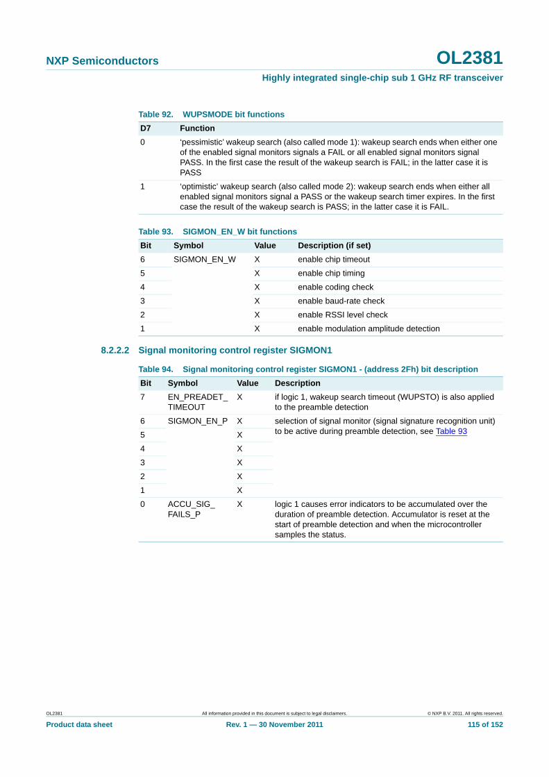
NXP Semiconductors OL2381Highly integrated single-chip sub 1 GHz RF transceiver
8.2.2.2 Signal monitoring control register SIGMON1
Table 92. WUPSMODE bit functions
D7 Function
0 ‘pessimistic’ wakeup search (also called mode 1): wakeup search ends when either one of the enabled signal monitors signals a FAIL or all enabled signal monitors signal PASS. In the first case the result of the wakeup search is FAIL; in the latter case it is PASS
1 ‘optimistic’ wakeup search (also called mode 2): wakeup search ends when either all enabled signal monitors signal a PASS or the wakeup search timer expires. In the first case the result of the wakeup search is PASS; in the latter case it is FAIL.
Table 93. SIGMON_EN_W bit functions
Bit Symbol Value Description (if set)
6 SIGMON_EN_W X enable chip timeout
5 X enable chip timing
4 X enable coding check
3 X enable baud-rate check
2 X enable RSSI level check
1 X enable modulation amplitude detection
Table 94. Signal monitoring control register SIGMON1 - (address 2Fh) bit description
Bit Symbol Value Description
7 EN_PREADET_TIMEOUT
X if logic 1, wakeup search timeout (WUPSTO) is also applied to the preamble detection
6 SIGMON_EN_P X selection of signal monitor (signal signature recognition unit) to be active during preamble detection, see Table 935 X
4 X
3 X
2 X
1 X
0 ACCU_SIG_FAILS_P
X logic 1 causes error indicators to be accumulated over the duration of preamble detection. Accumulator is reset at the start of preamble detection and when the microcontroller samples the status.
OL2381 All information provided in this document is subject to legal disclaimers. © NXP B.V. 2011. All rights reserved.
Product data sheet Rev. 1 — 30 November 2011 115 of 152
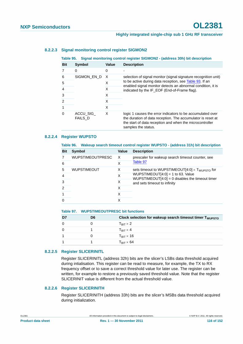
NXP Semiconductors OL2381Highly integrated single-chip sub 1 GHz RF transceiver
8.2.2.3 Signal monitoring control register SIGMON2
8.2.2.4 Register WUPSTO
8.2.2.5 Register SLICERINITL
Register SLICERINITL (address 32h) bits are the slicer’s LSBs data threshold acquired during intialisation. This register can be read to measure, for example, the TX to RX frequency offset or to save a correct threshold value for later use. The register can be written, for example to restore a previously saved threshold value. Note that the register SLICERINIT value is different from the actual threshold value.
8.2.2.6 Register SLICERINITH
Register SLICERINITH (address 33h) bits are the slicer’s MSBs data threshold acquired during initialization.
Table 95. Signal monitoring control register SIGMON2 - (address 30h) bit description
Bit Symbol Value Description
7 0 0 -
6 SIGMON_EN_D X selection of signal monitor (signal signature recognition unit) to be active during data reception, see Table 93. If an enabled signal monitor detects an abnormal condition, it is indicated by the IF_EOF (End-of-Frame flag).
5 X
4 X
3 X
2 X
1 X
0 ACCU_SIG_FAILS_D
X logic 1 causes the error indicators to be accumulated over the duration of data reception. The accumulator is reset at the start of data reception and when the microcontroller samples the status.
Table 96. Wakeup search timeout control register WUPSTO - (address 31h) bit description
Bit Symbol Value Description
7 WUPSTIMEOUTPRESC X prescaler for wakeup search timeout counter, see Table 976 X
5 WUPSTIMEOUT X sets timeout to WUPSTIMEOUT[4:0] TWUPSTO for WUPSTIMEOUT[4:0] = 1 to 63. Value WUPSTIMEOUT[4:0] = 0 disables the timeout timer and sets timeout to infinity
4 X
3 X
2 X
1 X
0 X
Table 97. WUPSTIMEOUTPRESC bit functions
D7 D6 Clock selection for wakeup search timeout timer TWUPSTO
0 0 TBIT 2
0 1 TBIT 4
1 0 TBIT 16
1 1 TBIT 64
OL2381 All information provided in this document is subject to legal disclaimers. © NXP B.V. 2011. All rights reserved.
Product data sheet Rev. 1 — 30 November 2011 116 of 152

NXP Semiconductors OL2381Highly integrated single-chip sub 1 GHz RF transceiver
8.2.2.7 Register TIMINGCHK
Register TIMINGCHK (address 34h) configures the timing-check units.
Table 98. Register TIMINGCHK - (address 34h) bit description
Bit Symbol Value Description
7 RFU X reserved
6 BROBSLENGTH X baud rate observation length setting: number of observed bits configurable to 8, 16, 24 or 32 bits, see Table 995 X
4 SUMBITTMGERRTH X baud-rate checker threshold value for the sum of 8-bits timing, see Table 1003 X
2 X
1 SGLBITTMGERRTH X single chip timing check threshold value. The time interval is accepted if its absolute value is below the limit. Corresponds to timing errors which are less than 12.5 %, 18.75 %, 25 % or 37.5% of a nominal chip width respectively; see Table 101
0 X
Table 99. BROBSLENGTH bit functions
D6 D5 Number of nominal bits to be considered for baud-rate checker
0 0 8
0 1 16
1 0 24
1 1 32
Table 100. SUMBITTMGERRTH bit functions
D4 D3 D2 Total timing error threshold in TCHIP / 128 per 8 bits
Relative limit with respect to 8 nominal bits (%)
0 0 0 16 0.78
0 0 1 24 1.17
0 1 0 32 1.56
0 1 1 48 2.34
1 0 0 64 3.13
1 0 1 96 4.69
1 1 0 128 6.25
1 1 1 192 9.38
Table 101. SGLBITTMGERRTH bit functions
D1 D0 Single chip timing error threshold in TCHIP / 128 per interval
0 0 16
0 1 24
1 0 32
1 1 48
OL2381 All information provided in this document is subject to legal disclaimers. © NXP B.V. 2011. All rights reserved.
Product data sheet Rev. 1 — 30 November 2011 117 of 152
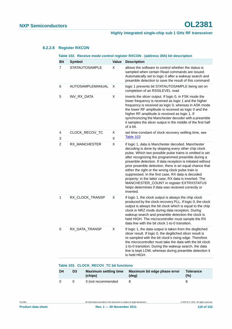
NXP Semiconductors OL2381Highly integrated single-chip sub 1 GHz RF transceiver
8.2.2.8 Register RXCON
Table 102. Receive mode control register RXCON - (address 35h) bit description
Bit Symbol Value Description
7 STATAUTOSAMPLE X allows the software to control whether the status is sampled when certain Read commands are issued. Automatically set to logic 0 after a wakeup search and preamble detection to save the result of this command
6 AUTOSAMPLEMANUAL X logic 1 prevents bit STATAUTOSAMPLE being set on completion of an RSSILEVEL read
5 INV_RX_DATA X inverts the slicer output. If logic 0, in FSK mode the lower frequency is received as logic 1 and the higher frequency is received as logic 0, whereas in ASK mode the lower RF amplitude is received as logic 0 and the higher RF amplitude is received as logic 1. If synchronizing the Manchester decoder with a preamble it samples the slicer output in the middle of the first half of a bit.
4 CLOCK_RECOV_TC X set time-constant of clock recovery settling time, see Table 1033 X
2 RX_MANCHESTER X if logic 1, data is Manchester decoded. Manchester decoding is done by skipping every other chip clock pulse. Which two possible pulse trains is omitted is set after recognizing the programmed preamble during a preamble detection. If data reception is initiated without prior preamble detection, there is an equal chance that either the right or the wrong clock pulse train is suppressed. In the first case, RX data is decoded properly; in the latter case, RX data is inverted. The MANCHESTER_COUNT in register EXTRXSTATUS helps determines if data was received correctly or inverted.
1 RX_CLOCK_TRANSP X if logic 1, the clock output is always the chip clock produced by the clock recovery PLL. If logic 0, the clock output is always the bit clock which is equal to the chip clock in NRZ mode during data reception. During wakeup search and preamble detection the clock is held HIGH. The microcontroller must sample the RX data line with the bit clock 1-to-0 transition.
0 RX_DATA_TRANSP X If logic 1, the data output is taken from the deglitched slicer result. If logic 0, the deglitched slicer result is re-sampled with the bit clock’s rising edge. Therefore the microcontroller must take the data with the bit clock 1-to-0 transition. During the wakeup search, the data line is kept LOW, whereas during preamble detection it is held HIGH.
Table 103. CLOCK_RECOV_TC bit functions
D4 D3 Maximum settling time(chips)
Maximum bit edge phase error (deg)
Tolerance(%)
0 0 3 (not recommended 8 8
OL2381 All information provided in this document is subject to legal disclaimers. © NXP B.V. 2011. All rights reserved.
Product data sheet Rev. 1 — 30 November 2011 118 of 152
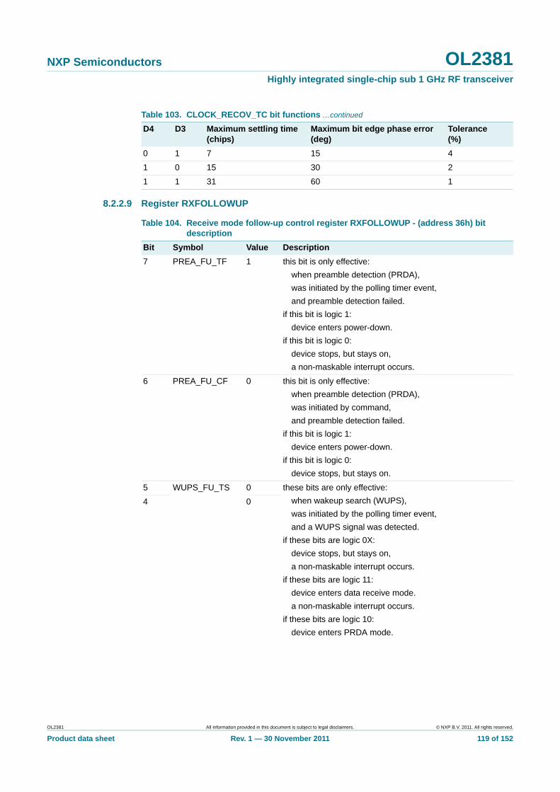
NXP Semiconductors OL2381Highly integrated single-chip sub 1 GHz RF transceiver
8.2.2.9 Register RXFOLLOWUP
0 1 7 15 4
1 0 15 30 2
1 1 31 60 1
Table 103. CLOCK_RECOV_TC bit functions …continued
D4 D3 Maximum settling time(chips)
Maximum bit edge phase error (deg)
Tolerance(%)
Table 104. Receive mode follow-up control register RXFOLLOWUP - (address 36h) bit description
Bit Symbol Value Description
7 PREA_FU_TF 1 this bit is only effective:
when preamble detection (PRDA),
was initiated by the polling timer event,
and preamble detection failed.
if this bit is logic 1:
device enters power-down.
if this bit is logic 0:
device stops, but stays on,
a non-maskable interrupt occurs.
6 PREA_FU_CF 0 this bit is only effective:
when preamble detection (PRDA),
was initiated by command,
and preamble detection failed.
if this bit is logic 1:
device enters power-down.
if this bit is logic 0:
device stops, but stays on.
5 WUPS_FU_TS 0 these bits are only effective:
when wakeup search (WUPS),
was initiated by the polling timer event,
and a WUPS signal was detected.
if these bits are logic 0X:
device stops, but stays on,
a non-maskable interrupt occurs.
if these bits are logic 11:
device enters data receive mode.
a non-maskable interrupt occurs.
if these bits are logic 10:
device enters PRDA mode.
4 0
OL2381 All information provided in this document is subject to legal disclaimers. © NXP B.V. 2011. All rights reserved.
Product data sheet Rev. 1 — 30 November 2011 119 of 152
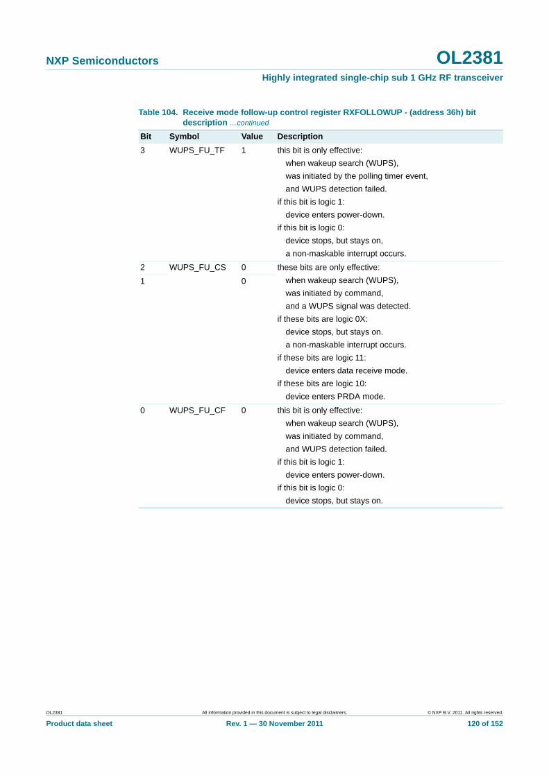
NXP Semiconductors OL2381Highly integrated single-chip sub 1 GHz RF transceiver
3 WUPS_FU_TF 1 this bit is only effective:
when wakeup search (WUPS),
was initiated by the polling timer event,
and WUPS detection failed.
if this bit is logic 1:
device enters power-down.
if this bit is logic 0:
device stops, but stays on,
a non-maskable interrupt occurs.
2 WUPS_FU_CS 0 these bits are only effective:
when wakeup search (WUPS),
was initiated by command,
and a WUPS signal was detected.
if these bits are logic 0X:
device stops, but stays on.
a non-maskable interrupt occurs.
if these bits are logic 11:
device enters data receive mode.
if these bits are logic 10:
device enters PRDA mode.
1 0
0 WUPS_FU_CF 0 this bit is only effective:
when wakeup search (WUPS),
was initiated by command,
and WUPS detection failed.
if this bit is logic 1:
device enters power-down.
if this bit is logic 0:
device stops, but stays on.
Table 104. Receive mode follow-up control register RXFOLLOWUP - (address 36h) bit description …continued
Bit Symbol Value Description
OL2381 All information provided in this document is subject to legal disclaimers. © NXP B.V. 2011. All rights reserved.
Product data sheet Rev. 1 — 30 November 2011 120 of 152
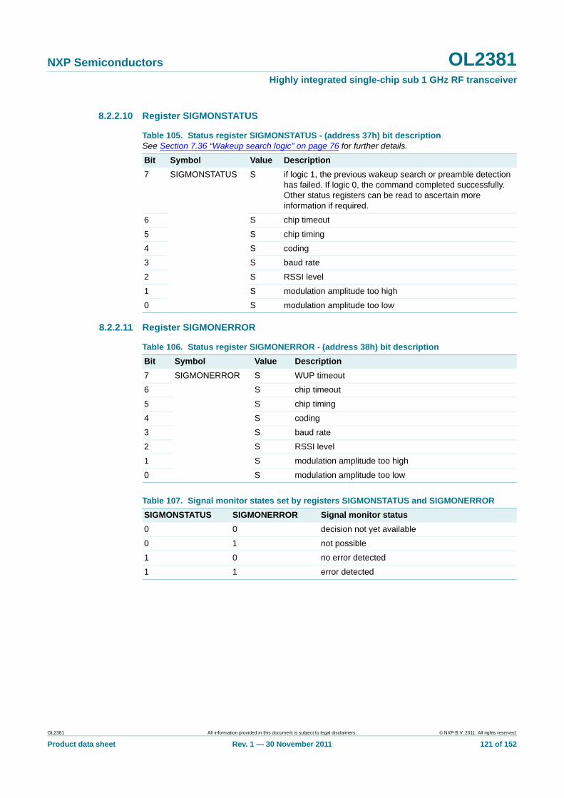
NXP Semiconductors OL2381Highly integrated single-chip sub 1 GHz RF transceiver
8.2.2.10 Register SIGMONSTATUS
8.2.2.11 Register SIGMONERROR
Table 105. Status register SIGMONSTATUS - (address 37h) bit descriptionSee Section 7.36 “Wakeup search logic” on page 76 for further details.
Bit Symbol Value Description
7 SIGMONSTATUS S if logic 1, the previous wakeup search or preamble detection has failed. If logic 0, the command completed successfully. Other status registers can be read to ascertain more information if required.
6 S chip timeout
5 S chip timing
4 S coding
3 S baud rate
2 S RSSI level
1 S modulation amplitude too high
0 S modulation amplitude too low
Table 106. Status register SIGMONERROR - (address 38h) bit description
Bit Symbol Value Description
7 SIGMONERROR S WUP timeout
6 S chip timeout
5 S chip timing
4 S coding
3 S baud rate
2 S RSSI level
1 S modulation amplitude too high
0 S modulation amplitude too low
Table 107. Signal monitor states set by registers SIGMONSTATUS and SIGMONERROR
SIGMONSTATUS SIGMONERROR Signal monitor status
0 0 decision not yet available
0 1 not possible
1 0 no error detected
1 1 error detected
OL2381 All information provided in this document is subject to legal disclaimers. © NXP B.V. 2011. All rights reserved.
Product data sheet Rev. 1 — 30 November 2011 121 of 152
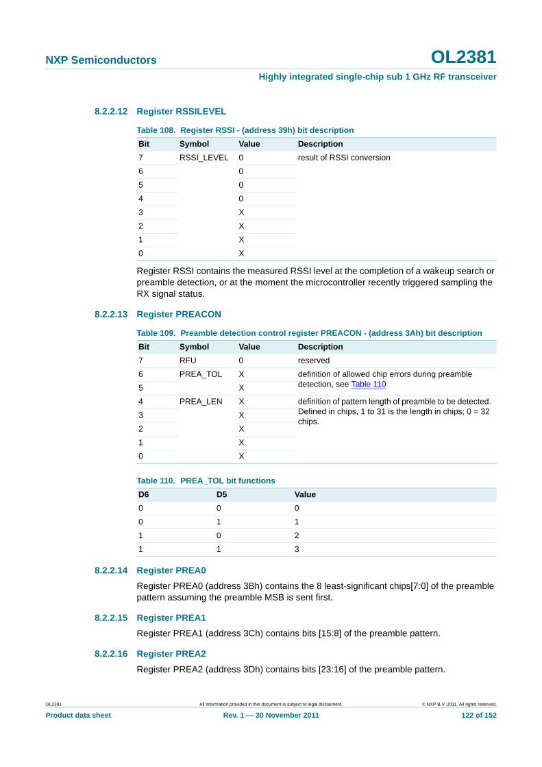
NXP Semiconductors OL2381Highly integrated single-chip sub 1 GHz RF transceiver
8.2.2.12 Register RSSILEVEL
Register RSSI contains the measured RSSI level at the completion of a wakeup search or preamble detection, or at the moment the microcontroller recently triggered sampling the RX signal status.
8.2.2.13 Register PREACON
8.2.2.14 Register PREA0
Register PREA0 (address 3Bh) contains the 8 least-significant chips[7:0] of the preamble pattern assuming the preamble MSB is sent first.
8.2.2.15 Register PREA1
Register PREA1 (address 3Ch) contains bits [15:8] of the preamble pattern.
8.2.2.16 Register PREA2
Register PREA2 (address 3Dh) contains bits [23:16] of the preamble pattern.
Table 108. Register RSSI - (address 39h) bit description
Bit Symbol Value Description
7 RSSI_LEVEL 0 result of RSSI conversion
6 0
5 0
4 0
3 X
2 X
1 X
0 X
Table 109. Preamble detection control register PREACON - (address 3Ah) bit description
Bit Symbol Value Description
7 RFU 0 reserved
6 PREA_TOL X definition of allowed chip errors during preamble detection, see Table 1105 X
4 PREA_LEN X definition of pattern length of preamble to be detected. Defined in chips, 1 to 31 is the length in chips; 0 = 32 chips.
3 X
2 X
1 X
0 X
Table 110. PREA_TOL bit functions
D6 D5 Value
0 0 0
0 1 1
1 0 2
1 1 3
OL2381 All information provided in this document is subject to legal disclaimers. © NXP B.V. 2011. All rights reserved.
Product data sheet Rev. 1 — 30 November 2011 122 of 152

NXP Semiconductors OL2381Highly integrated single-chip sub 1 GHz RF transceiver
8.2.2.17 Register PREA3
Register PREA3 (address 3Eh) contains bits [31:24] of the preamble pattern.
8.2.3 Registers only visible in bank 1
8.2.3.1 Register EXTRXSTATUS
8.2.3.2 Register CFRCCAL
8.2.3.3 Register CFIQCAL
Table 111. Register EXTRXSTATUS - (address 2Eh) bit description
Bit Symbol Value Description
7 RX_HIGH_GAIN S logic 1 when high gain is selected, logic 0 when low gain is selected (either automatically or by command)
6 LIVE_STATUS S logic 0 if the consistent set of status information is automatically sampled on completion of wakeup search or preamble detection. Logic 1 if the status was sampled by a Read operation from one of the 4 receiver status registers.
5 RX_CMD S RX sub-command code during which, or on completion, the status is sampled. 00 = IDLE, 01 = WUPS, 10 = PREA and 11 = DATA.
4 S
3 MANCHESTER_COUNT
S accumulated sum of RX data changes within a single chip period, see Section 7.38 “RX data decoding” on page 812 S
1 S
0 S
Table 112. Register CFRCCAL - (address 2Fh) bit description
Bit Symbol Value Description
7 CF_IQ_CAL_RUNNING S status bit indicates running IQ calibration
6 CF_CAL_RUNNING S status bit indicates running RC calibration
5 0 0 -
4 0 0 -
3 CF_RC_CAL_RES S result of RC auto-calibration
2 S
1 S
0 S
Table 113. IQ calibration register CFIQCAL - (address 30h) bit description
Bit Symbol Value Description
7 START_CF_IQ_CAL 0 setting this bits starts the I/Q calibration sequence
6 CF_IQ_CALVAL S configuration for the best I/Q calibration. The result of a triggered calibration sequence used in production test. Configuration value must be initialized and stored by the external microcontroller for every individual device to achieve best image rejection performance.
5 0
4 0
3 0
2 0
1 0
0 0
OL2381 All information provided in this document is subject to legal disclaimers. © NXP B.V. 2011. All rights reserved.
Product data sheet Rev. 1 — 30 November 2011 123 of 152
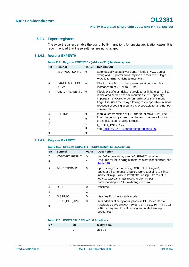
NXP Semiconductors OL2381Highly integrated single-chip sub 1 GHz RF transceiver
8.2.4 Expert registers
The expert registers enable the use of built-in functions for special application cases. It is recommended that these settings are not changed.
8.2.4.1 Register EXPERT0
8.2.4.2 Register EXPERT1
Table 114. Register EXPERT0 - (address 31h) bit description
Bit Symbol Value Description
7 RED_VCO_SWING 0 automatically set at lower band, if logic 1, VCO output swing and LO power consumption are reduced. If logic 0, VCO is running at highest drive level.
6 LARGE_PLL_RST_DELAY
0 if logic 1, the PLL phase detector reset pulse width is increased from 2.1 ns to 3.1 ns
5 FASTCFFILTSETTL 0 if logic 0, sufficient delay is provided until the channel filter is declared settled after an input transient. Especially important if a WUPS is performed in pessimistic mode. Logic 1 reduces the delay allowing faster operation. A small reduction of settling accuracy is acceptable for all other RX commands.
4 PLL_ICP 0 manual programming of PLL charge pump current. The final charge pump current can be computed as a function of the register setting using formula:
Icp = PLL_ICP 15 Asee Section 7.14.4 “Charge pump” on page 30.
3 0
2 1
1 0
0 0
Table 115. Register EXPERT1 - (address 32h) bit description
Bit Symbol Value Description
7 XOSTARTUPDELAY 0 sets/influences delay after XO_READY detection. Required for influencing automated startup sequences, see Table 116
6 1
5 ASKRSTBBMID 0 applies only when receiving ASK. If left at logic 0, baseband filter resets to logic 0 (corresponding to minus infinite dBm plus noise level) after an input transient. If logic 1, baseband filter resets to the mid-point corresponding to RSSI mid-range in dBm.
4 RFU 0 reserved
3 1
2 DISFRAC 0 disables PLL fractional-N mode
1 LOCK_DET_TIME 0 sets additional delay after ‘physical’ PLL lock detection. Available delays are: 00 = 16 s, 01 = 32 s, 10 = 48 s, 11 = 64 s, required for influencing automated startup sequences.
0 1
Table 116. XOSTARTUPDELAY bit functions
D7 D6 Delay time
0 0 256 s
OL2381 All information provided in this document is subject to legal disclaimers. © NXP B.V. 2011. All rights reserved.
Product data sheet Rev. 1 — 30 November 2011 124 of 152

NXP Semiconductors OL2381Highly integrated single-chip sub 1 GHz RF transceiver
8.2.4.3 Register EXPERT2
0 1 512 s (default Power-on reset value)
1 0 768 s
1 1 1024 s
Table 116. XOSTARTUPDELAY bit functions …continued
D7 D6 Delay time
Table 117. Register EXPERT2 - (address 33h) bit description
Bit Symbol Value Description
7 FM_DEM_IANDQ 0 if logic 1, I and Q limiter outputs are used for FSK demodulation
6 LARGE_FM_DEM_RANGE
0 logic 0 selects 200 kHz range (200 kHz to 400 kHz), logic 1 selects 600 kHz range (0 Hz to 600 kHz). 0 Hz is a theoretical value limited to the channel filter AC coupling lower corner frequency.
5 WIDE_AMPL_WINDOW 0 selects the number of samples window to be used for edge detection amplitude. Logic 0 selects 2 samples at 1 and +1 either side of center. Logic 1 selects 4 samples at 2, 1, +1 and +2 either side of center.
4 REDUCED_CHIP_TIMEOUT
0 selects timeout value for the chip timing verification block. Logic 0 selects 3.5 chips, logic 1 selects 2.5 chips.
3 TWORSSIMSBITSSLOW 0 determines time taken to acquire the 2 MSBs in the RSSI ADC. Logic 0 selects 3 clocks for bit 5 and 1 clock for bit 4. Logic 1 selects 2 clocks for bit 5 and 2 clocks for bit 4.
2 FASTRSSIFILTSETTL 0 controls the RSSI filter settling time. Logic 0 selects 4 time-constants settling to within 2 % of the last step. Logic 1 selects 2 time-constants settling to within 14 % of the last step.
1 CAPRSI 1 allows the RSSI analog data low-pass filter to be trimmed changing the filter capacitor values which affect the low-pass cut-off frequency, see Table 119
0 0
Table 118. FM demodulator configurations
D7 D6 Center frequency (kHz)
Input frequency range (kHz)
Maximum frequency deviation (kHz)
Number of delay elements
0 0 300 200 to 400 100 40
0 1 300 0 to 600 300 13
1 0 600 200 to 400 100 20
1 1 600 0 to 600 300 7
Table 119. CAPRSSI bit functions
D1 D0 Typical capacitor value (pF) Time-constant (R = 300 k typical)
0 0 0 0 (parasitics only)
OL2381 All information provided in this document is subject to legal disclaimers. © NXP B.V. 2011. All rights reserved.
Product data sheet Rev. 1 — 30 November 2011 125 of 152

NXP Semiconductors OL2381Highly integrated single-chip sub 1 GHz RF transceiver
8.2.4.4 Register EXPERT3
8.2.5 Test registers
The test register bits are initialized to logic 0 after power-up. Test registers must never be used in standard applications.
8.2.5.1 Register TEST0
0 1 2 0.6 s
1 0 5 1.5 s
1 1 12 4.8 s
Table 119. CAPRSSI bit functions …continued
D1 D0 Typical capacitor value (pF) Time-constant (R = 300 k typical)
Table 120. Register EXPERT3 - (address 34h) bit description
Bit Symbol Value Description
7 0 0 -
6 0 0 -
5 0 0 -
4 0 0 -
3 TESTBUFFERCAL 0 logic 1 turns the calibration path on. Required during test buffer calibration
2 ALLOWREGSWITCH 0 controls the behavior of the REG_xxx_ON test bits. If logic 0, the REG_xxx_ON bits are OR’d to the normal control lines allowing unconditional turn-on of selected regulators. If logic 1, the REG_xxx_ON bits replace the normal control lines allowing full control (on and off) of the regulators.
1 LTDIQPHASECAL 0 if logic 0, all possible matching combinations in the RX chain are attempted in order to achieve the best image rejection. If logic 1, certain phase trimming values are forbidden to eventually achieve a better overall performance over temperature.
0 DONOTDISTURBPTCAL 0 if logic 0, a polling timer calibration can run in parallel with the PLL startup. If logic 1, the PLL startup, when requested, is delayed until the polling timer calibration ends.
Table 121. Register TEST0 - (address 35h) bit description
Bit Symbol Value Description
7 CF_MULTITONE_EN 0 channel filter multi-tone testing
6 DIG_TEST_SEL 0 selects digital test signals to be used in conjunction with the P11C[3:0] and P12C[3:0] settings, see Section 8.2.1.7 on page 96 and Section 8.2.1.8 on page 97
5 0
4 0
3 RXD_DBG_SEL 0 selects digital test signals
2 0
1 0
0 0
OL2381 All information provided in this document is subject to legal disclaimers. © NXP B.V. 2011. All rights reserved.
Product data sheet Rev. 1 — 30 November 2011 126 of 152
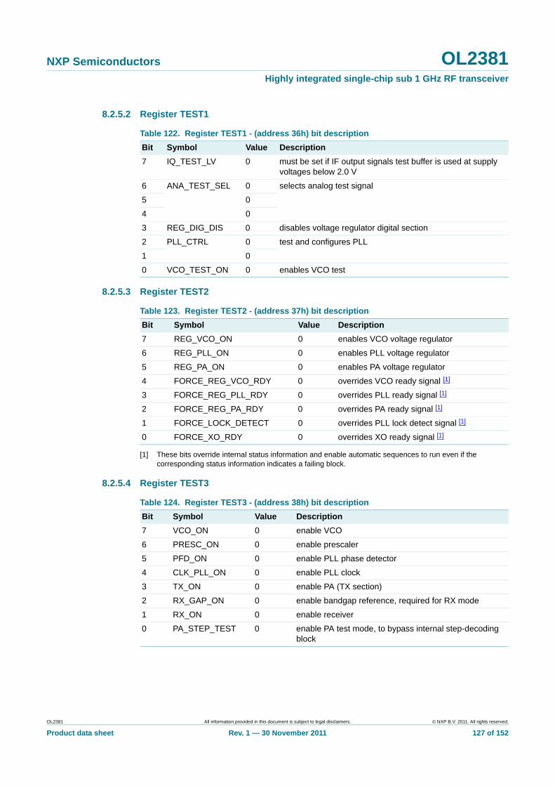
NXP Semiconductors OL2381Highly integrated single-chip sub 1 GHz RF transceiver
8.2.5.2 Register TEST1
8.2.5.3 Register TEST2
[1] These bits override internal status information and enable automatic sequences to run even if the corresponding status information indicates a failing block.
8.2.5.4 Register TEST3
Table 122. Register TEST1 - (address 36h) bit description
Bit Symbol Value Description
7 IQ_TEST_LV 0 must be set if IF output signals test buffer is used at supply voltages below 2.0 V
6 ANA_TEST_SEL 0 selects analog test signal
5 0
4 0
3 REG_DIG_DIS 0 disables voltage regulator digital section
2 PLL_CTRL 0 test and configures PLL
1 0
0 VCO_TEST_ON 0 enables VCO test
Table 123. Register TEST2 - (address 37h) bit description
Bit Symbol Value Description
7 REG_VCO_ON 0 enables VCO voltage regulator
6 REG_PLL_ON 0 enables PLL voltage regulator
5 REG_PA_ON 0 enables PA voltage regulator
4 FORCE_REG_VCO_RDY 0 overrides VCO ready signal [1]
3 FORCE_REG_PLL_RDY 0 overrides PLL ready signal [1]
2 FORCE_REG_PA_RDY 0 overrides PA ready signal [1]
1 FORCE_LOCK_DETECT 0 overrides PLL lock detect signal [1]
0 FORCE_XO_RDY 0 overrides XO ready signal [1]
Table 124. Register TEST3 - (address 38h) bit description
Bit Symbol Value Description
7 VCO_ON 0 enable VCO
6 PRESC_ON 0 enable prescaler
5 PFD_ON 0 enable PLL phase detector
4 CLK_PLL_ON 0 enable PLL clock
3 TX_ON 0 enable PA (TX section)
2 RX_GAP_ON 0 enable bandgap reference, required for RX mode
1 RX_ON 0 enable receiver
0 PA_STEP_TEST 0 enable PA test mode, to bypass internal step-decoding block
OL2381 All information provided in this document is subject to legal disclaimers. © NXP B.V. 2011. All rights reserved.
Product data sheet Rev. 1 — 30 November 2011 127 of 152
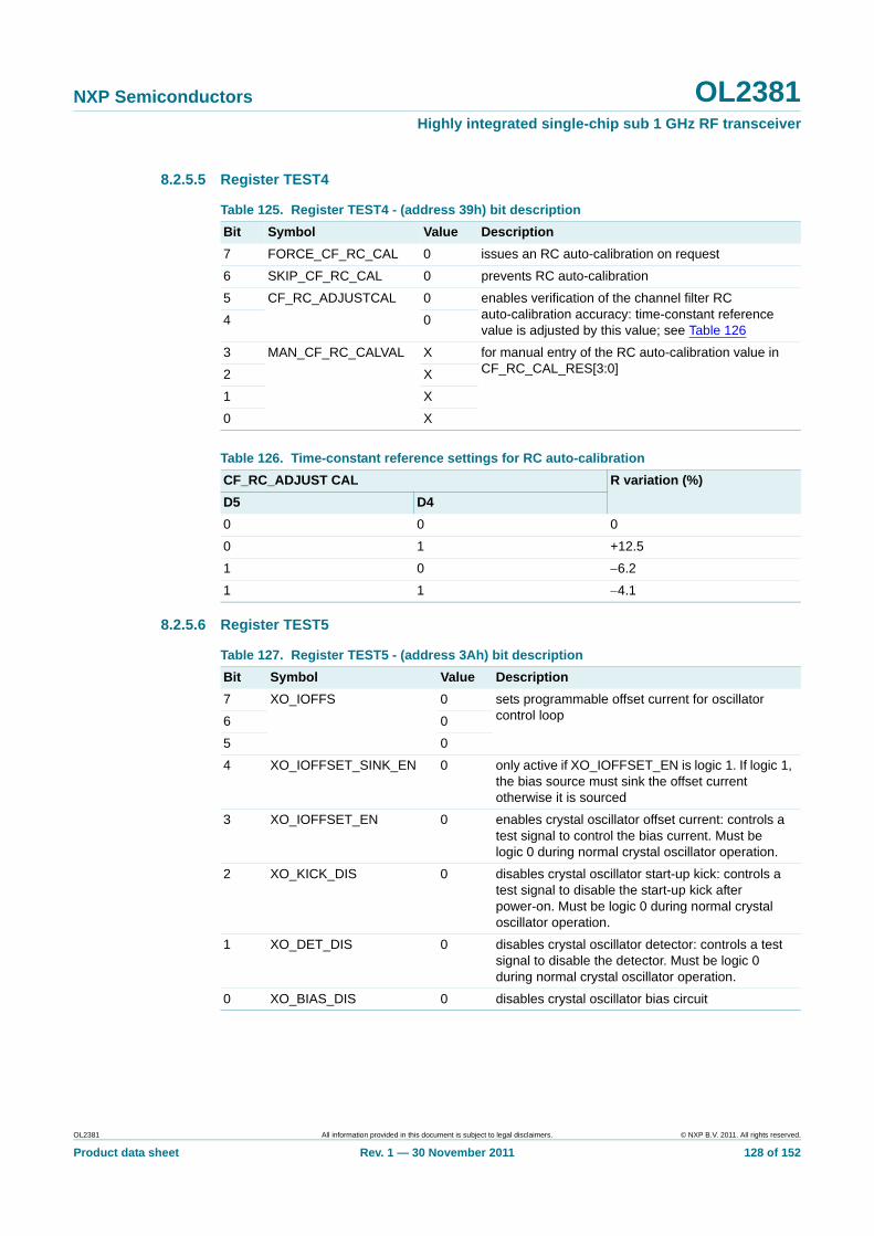
NXP Semiconductors OL2381Highly integrated single-chip sub 1 GHz RF transceiver
8.2.5.5 Register TEST4
8.2.5.6 Register TEST5
Table 125. Register TEST4 - (address 39h) bit description
Bit Symbol Value Description
7 FORCE_CF_RC_CAL 0 issues an RC auto-calibration on request
6 SKIP_CF_RC_CAL 0 prevents RC auto-calibration
5 CF_RC_ADJUSTCAL 0 enables verification of the channel filter RC auto-calibration accuracy: time-constant reference value is adjusted by this value; see Table 126
4 0
3 MAN_CF_RC_CALVAL X for manual entry of the RC auto-calibration value in CF_RC_CAL_RES[3:0]2 X
1 X
0 X
Table 126. Time-constant reference settings for RC auto-calibration
CF_RC_ADJUST CAL R variation (%)
D5 D4
0 0 0
0 1 +12.5
1 0 6.2
1 1 4.1
Table 127. Register TEST5 - (address 3Ah) bit description
Bit Symbol Value Description
7 XO_IOFFS 0 sets programmable offset current for oscillator control loop6 0
5 0
4 XO_IOFFSET_SINK_EN 0 only active if XO_IOFFSET_EN is logic 1. If logic 1, the bias source must sink the offset current otherwise it is sourced
3 XO_IOFFSET_EN 0 enables crystal oscillator offset current: controls a test signal to control the bias current. Must be logic 0 during normal crystal oscillator operation.
2 XO_KICK_DIS 0 disables crystal oscillator start-up kick: controls a test signal to disable the start-up kick after power-on. Must be logic 0 during normal crystal oscillator operation.
1 XO_DET_DIS 0 disables crystal oscillator detector: controls a test signal to disable the detector. Must be logic 0 during normal crystal oscillator operation.
0 XO_BIAS_DIS 0 disables crystal oscillator bias circuit
OL2381 All information provided in this document is subject to legal disclaimers. © NXP B.V. 2011. All rights reserved.
Product data sheet Rev. 1 — 30 November 2011 128 of 152
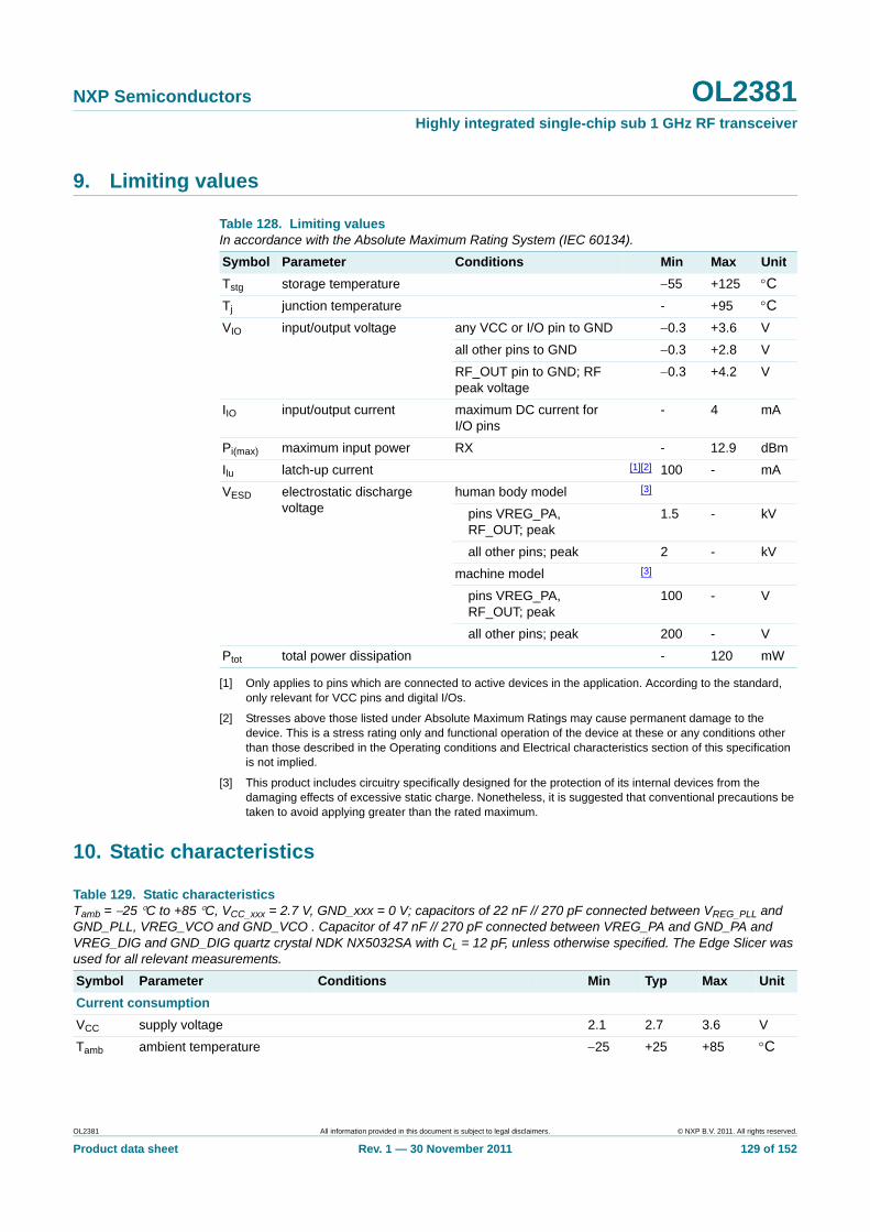
NXP Semiconductors OL2381Highly integrated single-chip sub 1 GHz RF transceiver
9. Limiting values
[1] Only applies to pins which are connected to active devices in the application. According to the standard, only relevant for VCC pins and digital I/Os.
[2] Stresses above those listed under Absolute Maximum Ratings may cause permanent damage to the device. This is a stress rating only and functional operation of the device at these or any conditions other than those described in the Operating conditions and Electrical characteristics section of this specification is not implied.
[3] This product includes circuitry specifically designed for the protection of its internal devices from the damaging effects of excessive static charge. Nonetheless, it is suggested that conventional precautions be taken to avoid applying greater than the rated maximum.
10. Static characteristics
Table 128. Limiting valuesIn accordance with the Absolute Maximum Rating System (IEC 60134).
Symbol Parameter Conditions Min Max Unit
Tstg storage temperature 55 +125 C
Tj junction temperature - +95 C
VIO input/output voltage any VCC or I/O pin to GND 0.3 +3.6 V
all other pins to GND 0.3 +2.8 V
RF_OUT pin to GND; RF peak voltage
0.3 +4.2 V
IIO input/output current maximum DC current for I/O pins
- 4 mA
Pi(max) maximum input power RX - 12.9 dBm
Ilu latch-up current [1][2] 100 - mA
VESD electrostatic discharge voltage
human body model [3]
pins VREG_PA, RF_OUT; peak
1.5 - kV
all other pins; peak 2 - kV
machine model [3]
pins VREG_PA, RF_OUT; peak
100 - V
all other pins; peak 200 - V
Ptot total power dissipation - 120 mW
Table 129. Static characteristicsTamb = 25 C to +85 C, VCC_xxx = 2.7 V, GND_xxx = 0 V; capacitors of 22 nF // 270 pF connected between VREG_PLL and GND_PLL, VREG_VCO and GND_VCO . Capacitor of 47 nF // 270 pF connected between VREG_PA and GND_PA and VREG_DIG and GND_DIG quartz crystal NDK NX5032SA with CL = 12 pF, unless otherwise specified. The Edge Slicer was used for all relevant measurements.
Symbol Parameter Conditions Min Typ Max Unit
Current consumption
VCC supply voltage 2.1 2.7 3.6 V
Tamb ambient temperature 25 +25 +85 C
OL2381 All information provided in this document is subject to legal disclaimers. © NXP B.V. 2011. All rights reserved.
Product data sheet Rev. 1 — 30 November 2011 129 of 152
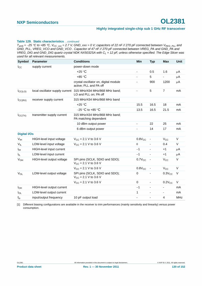
NXP Semiconductors OL2381Highly integrated single-chip sub 1 GHz RF transceiver
[1] Different biasing configurations are available in the receiver to trim performances (mainly sensitivity and linearity) versus power consumption.
ICC supply current power-down mode
+25 C - 0.5 1.6 A
+85 C - 5 - A
crystal oscillator on, digital module active; PLL and PA off
- 900 1200 A
ICC(LO) local oscillator supply current 315 MHz/434 MHz/868 MHz band; LO and PLL on; PA off
- 5 7 mA
ICC(RX) receiver supply current 315 MHz/434 MHz/868 MHz band
+25 C 15.5 16.5 18 mA
25 C to +85 C 13.5 16.5 21.5 mA
ICC(TX) transmitter supply current 315 MHz/434 MHz/868 MHz band; PA matching dependent
10 dBm output power - 22 25 mA
6 dBm output power - 14 17 mA
Digital I/Os
VIH HIGH-level input voltage VCC = 2.1 V to 3.6 V 0.8VCC - VCC V
VIL LOW-level input voltage VCC = 2.1 V to 3.6 V - 0.4 V
IIH HIGH-level input current 1 - +1 A
IIL LOW-level input current 1 - +1 A
VOH HIGH-level output voltage SPI pins (SCLK, SDIO and SDO); VCC = 2.1 V to 3.6 V
0.7VCC - VCC V
VCC = 2.1 V to 3.6 V 0.8VCC - VCC V
VOL LOW-level output voltage SPI pins (SCLK, SDIO and SDO); VCC = 2.1 V to 3.6 V
0 - 0.3VCC V
VCC = 2.1 V to 3.6 V 0 - 0.2VCC V
IOH HIGH-level output current 1 - - mA
IOL LOW-level output current 1 - - mA
fio input/output frequency 10 pF output load - - 4 MHz
Table 129. Static characteristics …continuedTamb = 25 C to +85 C, VCC_xxx = 2.7 V, GND_xxx = 0 V; capacitors of 22 nF // 270 pF connected between VREG_PLL and GND_PLL, VREG_VCO and GND_VCO . Capacitor of 47 nF // 270 pF connected between VREG_PA and GND_PA and VREG_DIG and GND_DIG quartz crystal NDK NX5032SA with CL = 12 pF, unless otherwise specified. The Edge Slicer was used for all relevant measurements.
Symbol Parameter Conditions Min Typ Max Unit
OL2381 All information provided in this document is subject to legal disclaimers. © NXP B.V. 2011. All rights reserved.
Product data sheet Rev. 1 — 30 November 2011 130 of 152
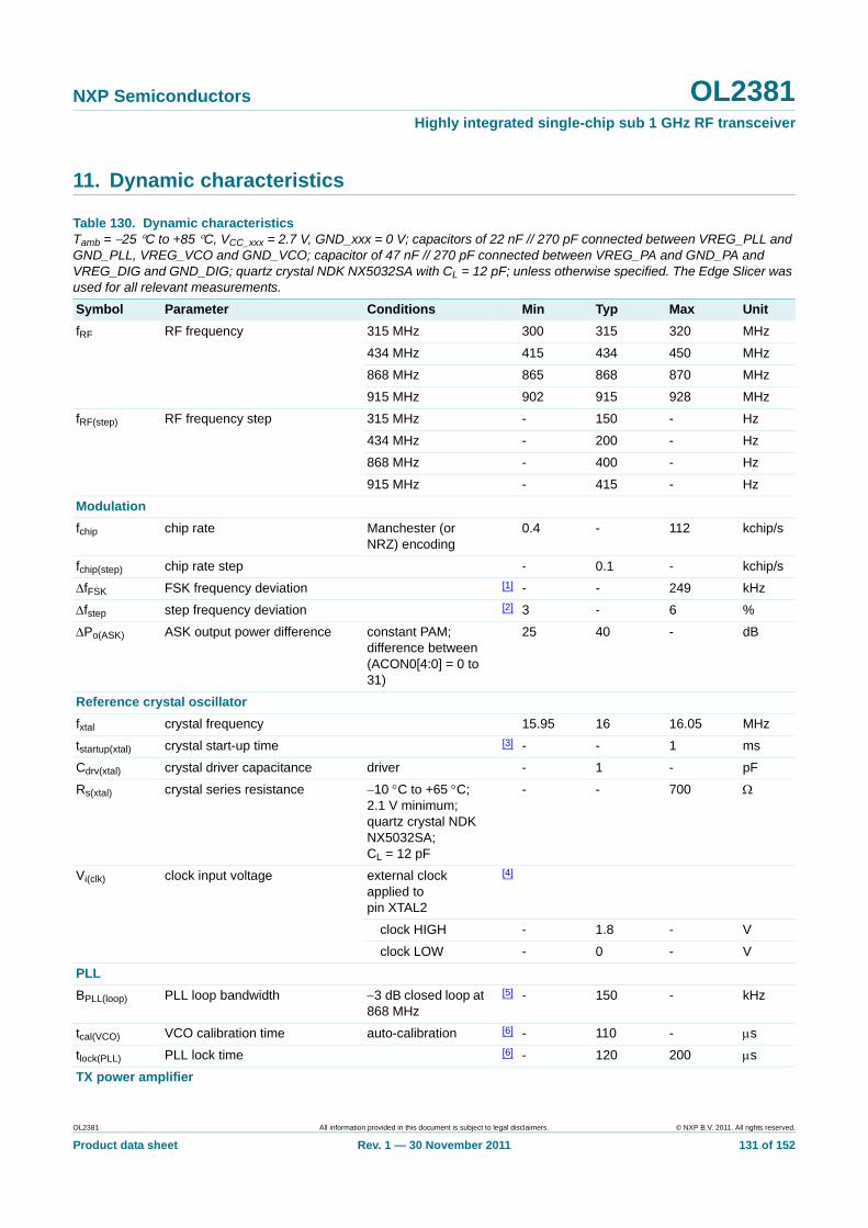
NXP Semiconductors OL2381Highly integrated single-chip sub 1 GHz RF transceiver
11. Dynamic characteristics
Table 130. Dynamic characteristicsTamb = 25 C to +85 C, VCC_xxx = 2.7 V, GND_xxx = 0 V; capacitors of 22 nF // 270 pF connected between VREG_PLL and GND_PLL, VREG_VCO and GND_VCO; capacitor of 47 nF // 270 pF connected between VREG_PA and GND_PA and VREG_DIG and GND_DIG; quartz crystal NDK NX5032SA with CL = 12 pF; unless otherwise specified. The Edge Slicer was used for all relevant measurements.
Symbol Parameter Conditions Min Typ Max Unit
fRF RF frequency 315 MHz 300 315 320 MHz
434 MHz 415 434 450 MHz
868 MHz 865 868 870 MHz
915 MHz 902 915 928 MHz
fRF(step) RF frequency step 315 MHz - 150 - Hz
434 MHz - 200 - Hz
868 MHz - 400 - Hz
915 MHz - 415 - Hz
Modulation
fchip chip rate Manchester (or NRZ) encoding
0.4 - 112 kchip/s
fchip(step) chip rate step - 0.1 - kchip/s
fFSK FSK frequency deviation [1] - - 249 kHz
fstep step frequency deviation [2] 3 - 6 %
Po(ASK) ASK output power difference constant PAM; difference between (ACON0[4:0] = 0 to 31)
25 40 - dB
Reference crystal oscillator
fxtal crystal frequency 15.95 16 16.05 MHz
tstartup(xtal) crystal start-up time [3] - - 1 ms
Cdrv(xtal) crystal driver capacitance driver - 1 - pF
Rs(xtal) crystal series resistance 10 C to +65 C; 2.1 V minimum; quartz crystal NDK NX5032SA; CL = 12 pF
- - 700
Vi(clk) clock input voltage external clock applied to pin XTAL2
[4]
clock HIGH - 1.8 - V
clock LOW - 0 - V
PLL
BPLL(loop) PLL loop bandwidth 3 dB closed loop at 868 MHz
[5] - 150 - kHz
tcal(VCO) VCO calibration time auto-calibration [6] - 110 - s
tlock(PLL) PLL lock time [6] - 120 200 s
TX power amplifier
OL2381 All information provided in this document is subject to legal disclaimers. © NXP B.V. 2011. All rights reserved.
Product data sheet Rev. 1 — 30 November 2011 131 of 152
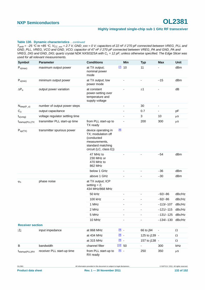
NXP Semiconductors OL2381Highly integrated single-chip sub 1 GHz RF transceiver
Po(max) maximum output power at TX output; nominal power mode
[7] 10 11 - dBm
Po(min) minimum output power at TX output; low power mode
- - 15 dBm
Po output power variation at constant power-setting over temperature and supply voltage
- 1 - dB
Nstep(P_o) number of output power steps - 30 -
Co output capacitance - 0.7 - pF
ts(vreg) voltage regulator settling time - 3 10 s
tstartup(PLL)TX transmitter PLL start-up time from PLL start-up to TX ready
- 200 300 s
Psp(TX) transmitter spurious power device operating in TX; modulation off (conducted measurements, standard matching circuit (LC, class E))
[8]
47 MHz to 230 MHz or 470 MHz to 862 MHz
- - 54 dBm
below 1 GHz - - 36 dBm
above 1 GHz - - 30 dBm
n phase noise at TX output; ICP setting = 2; 434 MHz/868 MHz
50 kHz - - 92/86 dBc/Hz
100 kHz - - 92/86 dBc/Hz
1 MHz - - 113/107 dBc/Hz
2 MHz - - 121/115 dBc/Hz
5 MHz - - 131/125 dBc/Hz
10 MHz - - 134/130 dBc/Hz
Receiver section
Zi input impedance at 868 MHz [9] - 66 to j94 -
at 434 MHz [9] - 125 to j139 -
at 315 MHz [9] - 157 to j138 -
B bandwidth channel filter [10] 50 - 300 kHz
tstartup(PLL)RX receiver PLL start-up time from PLL start-up to RX ready
[6] - 250 350 s
Table 130. Dynamic characteristics …continuedTamb = 25 C to +85 C, VCC_xxx = 2.7 V, GND_xxx = 0 V; capacitors of 22 nF // 270 pF connected between VREG_PLL and GND_PLL, VREG_VCO and GND_VCO; capacitor of 47 nF // 270 pF connected between VREG_PA and GND_PA and VREG_DIG and GND_DIG; quartz crystal NDK NX5032SA with CL = 12 pF; unless otherwise specified. The Edge Slicer was used for all relevant measurements.
Symbol Parameter Conditions Min Typ Max Unit
OL2381 All information provided in this document is subject to legal disclaimers. © NXP B.V. 2011. All rights reserved.
Product data sheet Rev. 1 — 30 November 2011 132 of 152

NXP Semiconductors OL2381Highly integrated single-chip sub 1 GHz RF transceiver
NF noise figure cascaded; maximum front-end gain
- 7 - dB
Table 130. Dynamic characteristics …continuedTamb = 25 C to +85 C, VCC_xxx = 2.7 V, GND_xxx = 0 V; capacitors of 22 nF // 270 pF connected between VREG_PLL and GND_PLL, VREG_VCO and GND_VCO; capacitor of 47 nF // 270 pF connected between VREG_PA and GND_PA and VREG_DIG and GND_DIG; quartz crystal NDK NX5032SA with CL = 12 pF; unless otherwise specified. The Edge Slicer was used for all relevant measurements.
Symbol Parameter Conditions Min Typ Max Unit
OL2381 All information provided in this document is subject to legal disclaimers. © NXP B.V. 2011. All rights reserved.
Product data sheet Rev. 1 — 30 November 2011 133 of 152
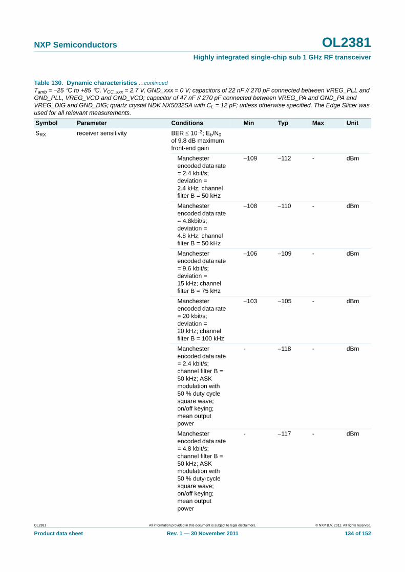
NXP Semiconductors OL2381Highly integrated single-chip sub 1 GHz RF transceiver
SRX receiver sensitivity BER 103; Eb/N0 of 9.8 dB maximum front-end gain
Manchester encoded data rate = 2.4 kbit/s; deviation = 2.4 kHz; channel filter B = 50 kHz
109 112 - dBm
Manchester encoded data rate = 4.8kbit/s; deviation = 4.8 kHz; channel filter B = 50 kHz
108 110 - dBm
Manchester encoded data rate = 9.6 kbit/s; deviation = 15 kHz; channel filter B = 75 kHz
106 109 - dBm
Manchester encoded data rate = 20 kbit/s; deviation = 20 kHz; channel filter B = 100 kHz
103 105 - dBm
Manchester encoded data rate = 2.4 kbit/s; channel filter B = 50 kHz; ASK modulation with 50 % duty cycle square wave; on/off keying; mean output power
- 118 - dBm
Manchester encoded data rate = 4.8 kbit/s; channel filter B = 50 kHz; ASK modulation with 50 % duty-cycle square wave; on/off keying; mean output power
- 117 - dBm
Table 130. Dynamic characteristics …continuedTamb = 25 C to +85 C, VCC_xxx = 2.7 V, GND_xxx = 0 V; capacitors of 22 nF // 270 pF connected between VREG_PLL and GND_PLL, VREG_VCO and GND_VCO; capacitor of 47 nF // 270 pF connected between VREG_PA and GND_PA and VREG_DIG and GND_DIG; quartz crystal NDK NX5032SA with CL = 12 pF; unless otherwise specified. The Edge Slicer was used for all relevant measurements.
Symbol Parameter Conditions Min Typ Max Unit
OL2381 All information provided in this document is subject to legal disclaimers. © NXP B.V. 2011. All rights reserved.
Product data sheet Rev. 1 — 30 November 2011 134 of 152
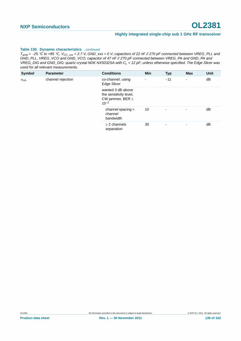
NXP Semiconductors OL2381Highly integrated single-chip sub 1 GHz RF transceiver
ch channel rejection co-channel; using Edge Slicer
- 11 - dB
wanted 3 dB above the sensitivity level, CW jammer, BER 102
channel spacing = channel bandwidth
10 - - dB
2 channels separation
30 - - dB
Table 130. Dynamic characteristics …continuedTamb = 25 C to +85 C, VCC_xxx = 2.7 V, GND_xxx = 0 V; capacitors of 22 nF // 270 pF connected between VREG_PLL and GND_PLL, VREG_VCO and GND_VCO; capacitor of 47 nF // 270 pF connected between VREG_PA and GND_PA and VREG_DIG and GND_DIG; quartz crystal NDK NX5032SA with CL = 12 pF; unless otherwise specified. The Edge Slicer was used for all relevant measurements.
Symbol Parameter Conditions Min Typ Max Unit
OL2381 All information provided in this document is subject to legal disclaimers. © NXP B.V. 2011. All rights reserved.
Product data sheet Rev. 1 — 30 November 2011 135 of 152
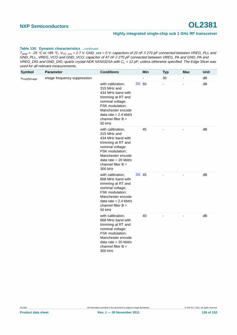
NXP Semiconductors OL2381Highly integrated single-chip sub 1 GHz RF transceiver
sup(f)image image frequency suppression - 30 - dB
with calibration, 315 MHz and 434 MHz band with trimming at RT and nominal voltage; FSK modulation; Manchester encode data rate = 2.4 kbit/s channel filter B = 50 kHz
[11] 50 - - dB
with calibration, 315 MHz and 434 MHz band with trimming at RT and nominal voltage; FSK modulation; Manchester encode data rate = 20 kbit/s channel filter B = 300 kHz
45 - - dB
with calibration, 868 MHz band with trimming at RT and nominal voltage; FSK modulation; Manchester encode data rate = 2.4 kbit/s channel filter B = 50 kHz
[11] 45 - - dB
with calibration, 868 MHz band with trimming at RT and nominal voltage; FSK modulation; Manchester encode data rate = 20 kbit/s channel filter B = 300 kHz
40 - - dB
Table 130. Dynamic characteristics …continuedTamb = 25 C to +85 C, VCC_xxx = 2.7 V, GND_xxx = 0 V; capacitors of 22 nF // 270 pF connected between VREG_PLL and GND_PLL, VREG_VCO and GND_VCO; capacitor of 47 nF // 270 pF connected between VREG_PA and GND_PA and VREG_DIG and GND_DIG; quartz crystal NDK NX5032SA with CL = 12 pF; unless otherwise specified. The Edge Slicer was used for all relevant measurements.
Symbol Parameter Conditions Min Typ Max Unit
OL2381 All information provided in this document is subject to legal disclaimers. © NXP B.V. 2011. All rights reserved.
Product data sheet Rev. 1 — 30 November 2011 136 of 152

NXP Semiconductors OL2381Highly integrated single-chip sub 1 GHz RF transceiver
ch(image) image channel rejection wanted 3 dB above the sensitivity level; CW jammer at image frequency; BER 102; calibration with external RF signal, FSK modulation
[11] - 22 - dB
315 MHz and 434 MHz; Manchester encoded data rate = 2.4 kbit/s; channel filter B = 50 kHz
[11] 40 - - dB
315 MHz and 434 MHz; Manchester encoded data rate = 20 kbit/s; channel filter B = 300 kHz
[11] 30 - - dB
868 MHz; Manchester encoded data rate = 2.4 kbit/s; channel filter B = 50 kHz
[11] 30 - - dB
868 MHz; Manchester encoded data rate = 20 kbit/s; channel filter B = 300 kHz
[11] 25 - - dB
oob out-of-band rejection blocking signal
1 MHz from edge band
40 - - dB
2 MHz from edge band
50 - - dB
5 MHz from edge band
60 - - dB
10 MHz from edge band
60 - - dB
ICP1dB 1 dB input compression point to mixer output; front-end maximum gain
- 36 - dBm
Table 130. Dynamic characteristics …continuedTamb = 25 C to +85 C, VCC_xxx = 2.7 V, GND_xxx = 0 V; capacitors of 22 nF // 270 pF connected between VREG_PLL and GND_PLL, VREG_VCO and GND_VCO; capacitor of 47 nF // 270 pF connected between VREG_PA and GND_PA and VREG_DIG and GND_DIG; quartz crystal NDK NX5032SA with CL = 12 pF; unless otherwise specified. The Edge Slicer was used for all relevant measurements.
Symbol Parameter Conditions Min Typ Max Unit
OL2381 All information provided in this document is subject to legal disclaimers. © NXP B.V. 2011. All rights reserved.
Product data sheet Rev. 1 — 30 November 2011 137 of 152
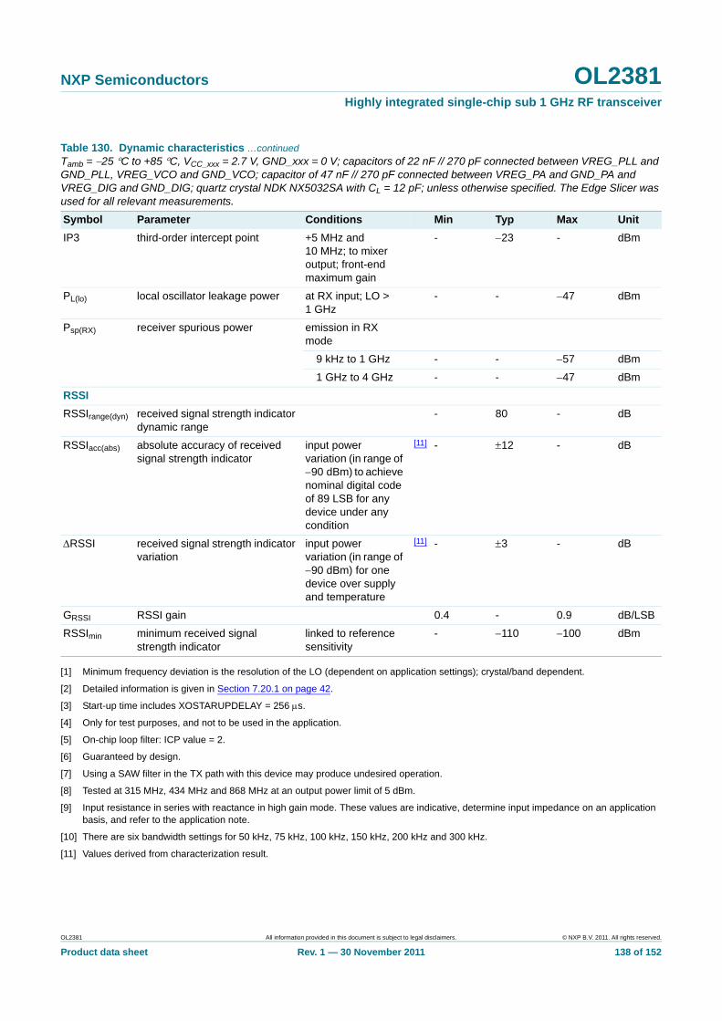
NXP Semiconductors OL2381Highly integrated single-chip sub 1 GHz RF transceiver
[1] Minimum frequency deviation is the resolution of the LO (dependent on application settings); crystal/band dependent.
[2] Detailed information is given in Section 7.20.1 on page 42.
[3] Start-up time includes XOSTARUPDELAY = 256 s.
[4] Only for test purposes, and not to be used in the application.
[5] On-chip loop filter: ICP value = 2.
[6] Guaranteed by design.
[7] Using a SAW filter in the TX path with this device may produce undesired operation.
[8] Tested at 315 MHz, 434 MHz and 868 MHz at an output power limit of 5 dBm.
[9] Input resistance in series with reactance in high gain mode. These values are indicative, determine input impedance on an application basis, and refer to the application note.
[10] There are six bandwidth settings for 50 kHz, 75 kHz, 100 kHz, 150 kHz, 200 kHz and 300 kHz.
[11] Values derived from characterization result.
IP3 third-order intercept point +5 MHz and 10 MHz; to mixer output; front-end maximum gain
- 23 - dBm
PL(lo) local oscillator leakage power at RX input; LO > 1 GHz
- - 47 dBm
Psp(RX) receiver spurious power emission in RX mode
9 kHz to 1 GHz - - 57 dBm
1 GHz to 4 GHz - - 47 dBm
RSSI
RSSIrange(dyn) received signal strength indicator dynamic range
- 80 - dB
RSSIacc(abs) absolute accuracy of received signal strength indicator
input power variation (in range of 90 dBm) to achieve nominal digital code of 89 LSB for any device under any condition
[11] - 12 - dB
RSSI received signal strength indicator variation
input power variation (in range of 90 dBm) for one device over supply and temperature
[11] - 3 - dB
GRSSI RSSI gain 0.4 - 0.9 dB/LSB
RSSImin minimum received signal strength indicator
linked to reference sensitivity
- 110 100 dBm
Table 130. Dynamic characteristics …continuedTamb = 25 C to +85 C, VCC_xxx = 2.7 V, GND_xxx = 0 V; capacitors of 22 nF // 270 pF connected between VREG_PLL and GND_PLL, VREG_VCO and GND_VCO; capacitor of 47 nF // 270 pF connected between VREG_PA and GND_PA and VREG_DIG and GND_DIG; quartz crystal NDK NX5032SA with CL = 12 pF; unless otherwise specified. The Edge Slicer was used for all relevant measurements.
Symbol Parameter Conditions Min Typ Max Unit
OL2381 All information provided in this document is subject to legal disclaimers. © NXP B.V. 2011. All rights reserved.
Product data sheet Rev. 1 — 30 November 2011 138 of 152

xxxx xxxxxxxxxxxxxxxxxxxxxxxxxxxxxx x xxxxxxxxxxxxxx xxxxxxxxxx xxx xxxxxx xxxxxxxxxxxxxxxxxxxxxxx xxxxxxxxxxxxxxxxxxxxxx xxxxx xxxxxx xx xxxxxxxxxxxxxxxxxxxxxxxxxxxxx xxxxxxxxxxxxxxxxxxxxxx xxxxxxxxxxx xxxxxxx xxxxxxxxxxxxxxxxxxx xxxxxxxxxxxxxxxx xxxxxxxxxxxxxx xxxxxx xx xxxxxxxxxxxxxxxxxxxxxxxxxxxxxxxx xxxxxxxxxxxxxxxxxxxxxxxx xxxxxxx xxxxxxxxxxxxxxxxxxxxxxxxxxxxxxxxxxxxxxxxxxxxxx xxxxxxxxxxx xxxxx x x
OL2
381
Pro
du
ct data sh
NX
P S
emico
nd
ucto
12. Ap
plicatio
n
VDD100 nF 100 nF 100 nF 100 nF 100 nF 100 nF
antenna
eet
_RE
GGND
_DIG
_XO
_RF
_IF
_PA
1 μF
rsO
L2381
Hig
hly
integ
rate
d sin
gle-ch
ip su
b 1
GH
z RF
tran
sc
eiver
info
rmatio
n
001aan636
nF
RFSWITCH
AD
DIT
ION
AL
FILT
ER
IF R
EQ
UIR
ED
AD
DIT
ION
AL
FILT
ER
IF R
EQ
UIR
ED
All information provid
ed in this documen
t is subject to legal disclaimers.
© N
XP
B.V
. 2011. A
ll rights reserved.
Rev. 1 —
30 No
vemb
er 2011 139 o
f 152
(1) The values for the matching circuit components must be finalized after test board layout.
All connections to GND must be separated.
Fig 53. Application diagram
OL2381
P14/PINDXTAL1
XTAL2
RSTDIS
SEN
SDIO
SCLK
P11/INT
P12/CLOCKP13/SDO
TEN
TEST1
TEST2
TEST3
VREG_DIG
VREG_VCO
VREG_PLL
VREG_PA
RF_OUT
RF_IN
GN
D(p
in1)
VC
C
VDD VC
C
VC
C
VC
C
VC
C
VC
C
GN
D(p
in8)
GN
D(p
in9)
expo
sed
die
pad
GN
D(p
in16
)
GN
D(p
in32
)SPI/DATA
OPTIONAL
47 nF
22 nF
47 nF
22
100 kΩ 100 kΩ 100 kΩ
P10/DATA

NXP Semiconductors OL2381Highly integrated single-chip sub 1 GHz RF transceiver
13. Package outline
Fig 54. Package outline SOT617-3 (HVQFN32)
ReferencesOutlineversion
Europeanprojection Issue date
IEC JEDEC JEITA
SOT617-3 MO-220
sot617-3_po
11-06-1411-06-21
Unit(1)
mmmaxnommin
0.850.05
0.000.2
5.1
4.9
3.75
3.45
5.1
4.9
3.75
3.450.5 3.5
A1
Dimensions
Note1. Plastic or metal protrusions of 0.075 mm maximum per side are not included.
HVQFN32: plastic thermal enhanced very thin quad flat package; no leads;32 terminals; body 5 x 5 x 0.85 mm SOT617-3
b c
0.30
0.18
D(1)A(1) Dh E(1) Eh e e1 e2 L
3.5
v w
0.1 0.1
y
0.050.5
0.3
y1
0.05
0 2.5 5 mm
scale
1/2 e
AC BvCw
terminal 1index area
AA1
detail X
yy1 Ce
L
Eh
Dh
e
e1
b9 16
32 25
24
178
1
X
D
E
C
B A
e2
terminal 1index area
1/2 e
OL2381 All information provided in this document is subject to legal disclaimers. © NXP B.V. 2011. All rights reserved.
Product data sheet Rev. 1 — 30 November 2011 140 of 152
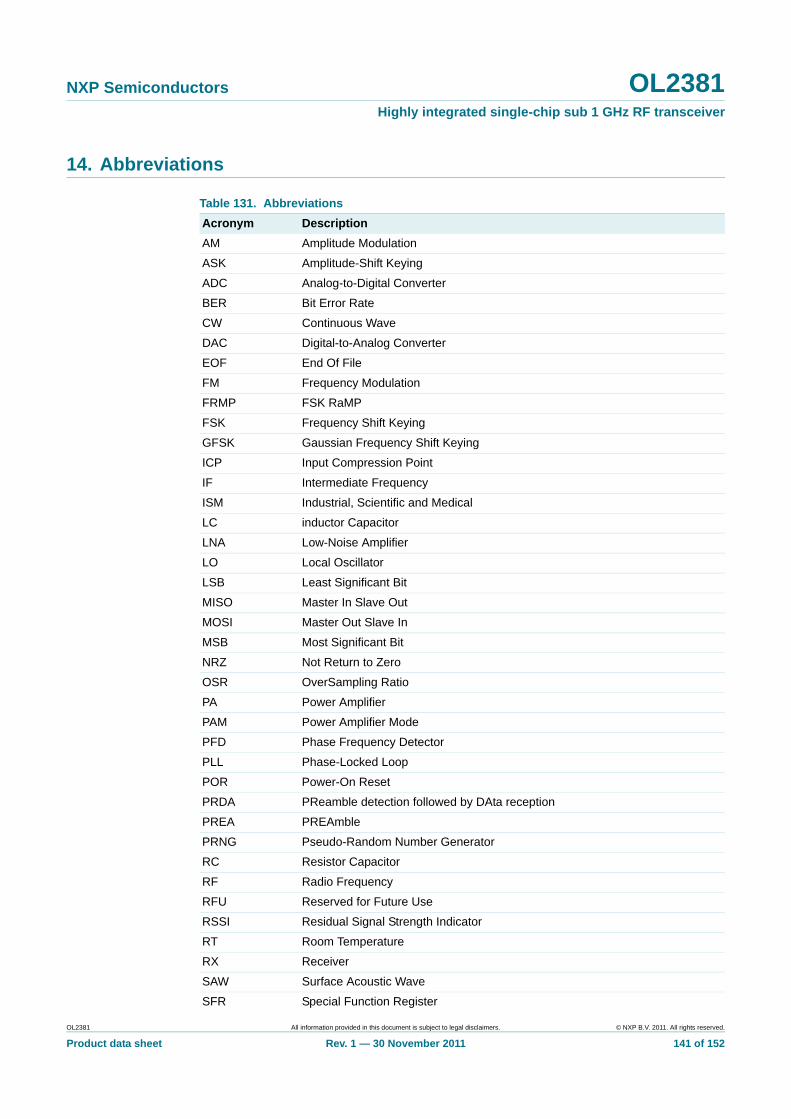
NXP Semiconductors OL2381Highly integrated single-chip sub 1 GHz RF transceiver
14. Abbreviations
Table 131. Abbreviations
Acronym Description
AM Amplitude Modulation
ASK Amplitude-Shift Keying
ADC Analog-to-Digital Converter
BER Bit Error Rate
CW Continuous Wave
DAC Digital-to-Analog Converter
EOF End Of File
FM Frequency Modulation
FRMP FSK RaMP
FSK Frequency Shift Keying
GFSK Gaussian Frequency Shift Keying
ICP Input Compression Point
IF Intermediate Frequency
ISM Industrial, Scientific and Medical
LC inductor Capacitor
LNA Low-Noise Amplifier
LO Local Oscillator
LSB Least Significant Bit
MISO Master In Slave Out
MOSI Master Out Slave In
MSB Most Significant Bit
NRZ Not Return to Zero
OSR OverSampling Ratio
PA Power Amplifier
PAM Power Amplifier Mode
PFD Phase Frequency Detector
PLL Phase-Locked Loop
POR Power-On Reset
PRDA PReamble detection followed by DAta reception
PREA PREAmble
PRNG Pseudo-Random Number Generator
RC Resistor Capacitor
RF Radio Frequency
RFU Reserved for Future Use
RSSI Residual Signal Strength Indicator
RT Room Temperature
RX Receiver
SAW Surface Acoustic Wave
SFR Special Function Register
OL2381 All information provided in this document is subject to legal disclaimers. © NXP B.V. 2011. All rights reserved.
Product data sheet Rev. 1 — 30 November 2011 141 of 152

NXP Semiconductors OL2381Highly integrated single-chip sub 1 GHz RF transceiver
SPI Serial Peripheral Interface
SRD Short-Range Device
TX Transmitter
VCO Voltage-Controlled Oscillator
WUP Wake UP
WUPS Wake UP Search
XO Crystal Oscillator
Table 131. Abbreviations …continued
Acronym Description
OL2381 All information provided in this document is subject to legal disclaimers. © NXP B.V. 2011. All rights reserved.
Product data sheet Rev. 1 — 30 November 2011 142 of 152

NXP Semiconductors OL2381Highly integrated single-chip sub 1 GHz RF transceiver
15. Revision history
Table 132. Revision history
Document ID Release date Data sheet status Change notice Supersedes
OL2381 v.1 20111130 Product data sheet - -
OL2381 All information provided in this document is subject to legal disclaimers. © NXP B.V. 2011. All rights reserved.
Product data sheet Rev. 1 — 30 November 2011 143 of 152
NXP Semiconductors OL2381Highly integrated single-chip sub 1 GHz RF transceiver
16. Legal information
16.1 Data sheet status
[1] Please consult the most recently issued document before initiating or completing a design.
[2] The term ‘short data sheet’ is explained in section “Definitions”.
[3] The product status of device(s) described in this document may have changed since this document was published and may differ in case of multiple devices. The latest product status information is available on the Internet at URL http://www.nxp.com.
16.2 Definitions
Draft — The document is a draft version only. The content is still under internal review and subject to formal approval, which may result in modifications or additions. NXP Semiconductors does not give any representations or warranties as to the accuracy or completeness of information included herein and shall have no liability for the consequences of use of such information.
Short data sheet — A short data sheet is an extract from a full data sheet with the same product type number(s) and title. A short data sheet is intended for quick reference only and should not be relied upon to contain detailed and full information. For detailed and full information see the relevant full data sheet, which is available on request via the local NXP Semiconductors sales office. In case of any inconsistency or conflict with the short data sheet, the full data sheet shall prevail.
Product specification — The information and data provided in a Product data sheet shall define the specification of the product as agreed between NXP Semiconductors and its customer, unless NXP Semiconductors and customer have explicitly agreed otherwise in writing. In no event however, shall an agreement be valid in which the NXP Semiconductors product is deemed to offer functions and qualities beyond those described in the Product data sheet.
16.3 Disclaimers
Limited warranty and liability — Information in this document is believed to be accurate and reliable. However, NXP Semiconductors does not give any representations or warranties, expressed or implied, as to the accuracy or completeness of such information and shall have no liability for the consequences of use of such information.
In no event shall NXP Semiconductors be liable for any indirect, incidental, punitive, special or consequential damages (including - without limitation - lost profits, lost savings, business interruption, costs related to the removal or replacement of any products or rework charges) whether or not such damages are based on tort (including negligence), warranty, breach of contract or any other legal theory.
Notwithstanding any damages that customer might incur for any reason whatsoever, NXP Semiconductors’ aggregate and cumulative liability towards customer for the products described herein shall be limited in accordance with the Terms and conditions of commercial sale of NXP Semiconductors.
Right to make changes — NXP Semiconductors reserves the right to make changes to information published in this document, including without limitation specifications and product descriptions, at any time and without notice. This document supersedes and replaces all information supplied prior to the publication hereof.
Suitability for use — NXP Semiconductors products are not designed, authorized or warranted to be suitable for use in life support, life-critical or safety-critical systems or equipment, nor in applications where failure or
malfunction of an NXP Semiconductors product can reasonably be expected to result in personal injury, death or severe property or environmental damage. NXP Semiconductors accepts no liability for inclusion and/or use of NXP Semiconductors products in such equipment or applications and therefore such inclusion and/or use is at the customer’s own risk.
Applications — Applications that are described herein for any of these products are for illustrative purposes only. NXP Semiconductors makes no representation or warranty that such applications will be suitable for the specified use without further testing or modification.
Customers are responsible for the design and operation of their applications and products using NXP Semiconductors products, and NXP Semiconductors accepts no liability for any assistance with applications or customer product design. It is customer’s sole responsibility to determine whether the NXP Semiconductors product is suitable and fit for the customer’s applications and products planned, as well as for the planned application and use of customer’s third party customer(s). Customers should provide appropriate design and operating safeguards to minimize the risks associated with their applications and products.
NXP Semiconductors does not accept any liability related to any default, damage, costs or problem which is based on any weakness or default in the customer’s applications or products, or the application or use by customer’s third party customer(s). Customer is responsible for doing all necessary testing for the customer’s applications and products using NXP Semiconductors products in order to avoid a default of the applications and the products or of the application or use by customer’s third party customer(s). NXP does not accept any liability in this respect.
Limiting values — Stress above one or more limiting values (as defined in the Absolute Maximum Ratings System of IEC 60134) will cause permanent damage to the device. Limiting values are stress ratings only and (proper) operation of the device at these or any other conditions above those given in the Recommended operating conditions section (if present) or the Characteristics sections of this document is not warranted. Constant or repeated exposure to limiting values will permanently and irreversibly affect the quality and reliability of the device.
Terms and conditions of commercial sale — NXP Semiconductors products are sold subject to the general terms and conditions of commercial sale, as published at http://www.nxp.com/profile/terms, unless otherwise agreed in a valid written individual agreement. In case an individual agreement is concluded only the terms and conditions of the respective agreement shall apply. NXP Semiconductors hereby expressly objects to applying the customer’s general terms and conditions with regard to the purchase of NXP Semiconductors products by customer.
No offer to sell or license — Nothing in this document may be interpreted or construed as an offer to sell products that is open for acceptance or the grant, conveyance or implication of any license under any copyrights, patents or other industrial or intellectual property rights.
Export control — This document as well as the item(s) described herein may be subject to export control regulations. Export might require a prior authorization from competent authorities.
Document status[1][2] Product status[3] Definition
Objective [short] data sheet Development This document contains data from the objective specification for product development.
Preliminary [short] data sheet Qualification This document contains data from the preliminary specification.
Product [short] data sheet Production This document contains the product specification.
OL2381 All information provided in this document is subject to legal disclaimers. © NXP B.V. 2011. All rights reserved.
Product data sheet Rev. 1 — 30 November 2011 144 of 152
NXP Semiconductors OL2381Highly integrated single-chip sub 1 GHz RF transceiver
Quick reference data — The Quick reference data is an extract of the product data given in the Limiting values and Characteristics sections of this document, and as such is not complete, exhaustive or legally binding.
Non-automotive qualified products — Unless this data sheet expressly states that this specific NXP Semiconductors product is automotive qualified, the product is not suitable for automotive use. It is neither qualified nor tested in accordance with automotive testing or application requirements. NXP Semiconductors accepts no liability for inclusion and/or use of non-automotive qualified products in automotive equipment or applications.
In the event that customer uses the product for design-in and use in automotive applications to automotive specifications and standards, customer (a) shall use the product without NXP Semiconductors’ warranty of the
product for such automotive applications, use and specifications, and (b) whenever customer uses the product for automotive applications beyond NXP Semiconductors’ specifications such use shall be solely at customer’s own risk, and (c) customer fully indemnifies NXP Semiconductors for any liability, damages or failed product claims resulting from customer design and use of the product for automotive applications beyond NXP Semiconductors’ standard warranty and NXP Semiconductors’ product specifications.
16.4 TrademarksNotice: All referenced brands, product names, service names and trademarks are the property of their respective owners.
17. Contact information
For more information, please visit: http://www.nxp.com
For sales office addresses, please send an email to: [email protected]
OL2381 All information provided in this document is subject to legal disclaimers. © NXP B.V. 2011. All rights reserved.
Product data sheet Rev. 1 — 30 November 2011 145 of 152

NXP Semiconductors OL2381Highly integrated single-chip sub 1 GHz RF transceiver
18. Tables
Table 1. Ordering information . . . . . . . . . . . . . . . . . . . . .2Table 2. Pin description . . . . . . . . . . . . . . . . . . . . . . . . . .4Table 3. Blocks with regulated supplies . . . . . . . . . . . . .19Table 4. TX command bits . . . . . . . . . . . . . . . . . . . . . . .35Table 5. TX command packet . . . . . . . . . . . . . . . . . . . .36Table 6. Control of TX data (bits TC, TE)[1] . . . . . . . . . .36Table 7. Power amplifier control and synchronization
(bits TC, TD) . . . . . . . . . . . . . . . . . . . . . . . . . .36Table 8. Summary of combined TC,
TD and TE bits . . . . . . . . . . . . . . . . . . . . . . . . .36Table 9. Amplitude selection
(bit TF) . . . . . . . . . . . . . . . . . . . . . . . . . . . . . . .36Table 10. Frequency band selection
(bits TA, TB) . . . . . . . . . . . . . . . . . . . . . . . . . . .37Table 11. Phase 1: data transmission . . . . . . . . . . . . . . .38Table 12. Phase 2: end data transmission . . . . . . . . . . .38Table 13. Channel filter gain settings . . . . . . . . . . . . . . .49Table 14. RX gain control . . . . . . . . . . . . . . . . . . . . . . . .49Table 15. Receive command packet . . . . . . . . . . . . . . . .55Table 16. Frequency selection (bits RA, RB) . . . . . . . . . .56Table 17. Sub-command selection bits RC, RD . . . . . . .56Table 18. Gain switch selection (bits RE, RF) . . . . . . . . .57Table 19. RXDCON registers . . . . . . . . . . . . . . . . . . . . .60Table 20. RX operating mode transitions . . . . . . . . . . . .61Table 21. Overview of the signal signature
recognition unit . . . . . . . . . . . . . . . . . . . . . . . . . . . . . . . . . .62
Table 22. Overview of signal monitoring methods . . . . . .77Table 23. Example 1: Using single byte reads . . . . . . . .79Table 24. Example 2: Using read command
auto-increment address . . . . . . . . . . . . . . . . . .80Table 25. FM demodulator configurations . . . . . . . . . . . .83Table 26. BASEBAND_FILTER_FC definition . . . . . . . . .85Table 27. Available RX debug signal vectors . . . . . . . . .86Table 28. Register map table . . . . . . . . . . . . . . . . . . . . . .89Table 29. Frequency control register FC0L -
(address 00h) bit description . . . . . . . . . . . . . .93Table 30. Frequency control register FC0M -
(address 01h) bit description . . . . . . . . . . . . . .93Table 31. Frequency control register FC0H -
(address 02h) bit description . . . . . . . . . . . . . .93Table 32. VCO control register VCOCON -
(address OCh) bit description . . . . . . . . . . . . .94Table 33. Local oscillator control register LOCON -
(address ODh) bit description . . . . . . . . . . . . .95Table 34. Timing register TIMING1 -
(address 0Fh) bit description . . . . . . . . . . . . . .95Table 35. Port control register PORTCON0 -
(address 10h) bit description . . . . . . . . . . . . . . 96Table 36. P10C port control data functions . . . . . . . . . . . 96Table 37. P11C port control data functions . . . . . . . . . . . 96Table 38. Test signal I . . . . . . . . . . . . . . . . . . . . . . . . . . . 97Table 39. Test signal II . . . . . . . . . . . . . . . . . . . . . . . . . . 97Table 40. Port control register PORTCON1 -
(address 11h) bit description . . . . . . . . . . . . . . 97Table 41. P12C port control data functions . . . . . . . . . . . 98Table 42. Test signal III . . . . . . . . . . . . . . . . . . . . . . . . . . 98Table 43. Test signal IIII . . . . . . . . . . . . . . . . . . . . . . . . . 98Table 44. P13C port control data functions . . . . . . . . . . . 99Table 45. Port control register PORTCON2 -
(address 12h) bit description . . . . . . . . . . . . . . 99Table 46. SEP_RX_OUT data functions . . . . . . . . . . . . . 99Table 47. SEP_TX_LINES data functions . . . . . . . . . . 100Table 48. P14C port control data functions . . . . . . . . . . 100Table 49. General power mode register
PWRMODE - (address 13h) bit description . . . . . . . . . . . . . . . . . . . . . . . . 100
Table 50. POLLTIM_EN data functions . . . . . . . . . . . . . 100Table 51. Polling timer status after master reset . . . . . . 101Table 52. DEV_MODE[1:0] device mode control
functions . . . . . . . . . . . . . . . . . . . . . . . . . . . . 101Table 53. Interrupt enable register IEN -
(address 14h) bit description . . . . . . . . . . . . . 101Table 54. Interrupt flag register IFLAG -
(address 15h) bit description . . . . . . . . . . . . . 102Table 55. Polling timer control register
POLLWUPTIME - (address 16h) bit description . . . . . . . . . . . . . . . . . . . . . . . . 102
Table 56. Polling action register POLLACTION - (address 17h) bit description . . . . . . . . . . . . . 102
Table 57. POLL_MODE[1:0] device mode control functions . . . . . . . . . . . . . . . . . . . . . . . . . . . . 103
Table 58. Clock connection register CLOCKCON - (address 18h) bit description . . . . . . . . . . . . . 103
Table 59. EXTPOLLTIMRNG bit functions . . . . . . . . . . 103Table 60. CLKSOURCESEL bit functions . . . . . . . . . . . 103Table 61. EXT_CLK_BUF_EN / XODIS bit functions . . 104Table 62. Device status register DEVSTATUS -
(address 19h) bit description . . . . . . . . . . . . . 104Table 63. FSK frequency deviation register FDEV -
(address 1Ah) bit description . . . . . . . . . . . . 104Table 64. FSK ramp adjustment register FRMP -
(address 1Bh) bit description . . . . . . . . . . . . 105Table 65. Register ACON0 - (address 1Ch)
bit description . . . . . . . . . . . . . . . . . . . . . . . . 105Table 66. Register ACON1 - (address 1Dh)
OL2381 All information provided in this document is subject to legal disclaimers. © NXP B.V. 2011. All rights reserved.
Product data sheet Rev. 1 — 30 November 2011 146 of 152
continued >>
NXP Semiconductors OL2381Highly integrated single-chip sub 1 GHz RF transceiver
bit description . . . . . . . . . . . . . . . . . . . . . . . .105Table 67. Register ACON2 - (address 1Eh) bit
description . . . . . . . . . . . . . . . . . . . . . . . . . . .106Table 68. Register ARMP - (address 1Fh) bit
description . . . . . . . . . . . . . . . . . . . . . . . . . . .106Table 69. Transmitter control register TXCON -
(address 20h) bit description . . . . . . . . . . . . .107Table 70. RX frequency offset . . . . . . . . . . . . . . . . . . . .107Table 71. Clock output selection for the TX command,
TXCLKOUTSEL . . . . . . . . . . . . . . . . . . . . . . .107Table 72. PAM definition[1] . . . . . . . . . . . . . . . . . . . . . . .107Table 73. Receiver gain control register RXGAIN -
(address 21h) bit description . . . . . . . . . . . . .108Table 74. Channel filter bandwidth and RSSI filter
settings register RXBW - (address 22h) bit description . . . . . . . . . . . . . . . . . . . . . . . .108
Table 75. CF_BW bit functions . . . . . . . . . . . . . . . . . . .108Table 76. Register GAINSTEP - (address 23h)
bit description . . . . . . . . . . . . . . . . . . . . . . . .109Table 77. Register HIGAINLIM - (address 24h)
bit description . . . . . . . . . . . . . . . . . . . . . . . .109Table 78. Register RXBBCON - (address 27h)
bit description . . . . . . . . . . . . . . . . . . . . . . . .109Table 79. DEGLITCHER_WINDOW_LEN bit functions . 110Table 80. Register UMODAMPTH - (address 28h)
bit description . . . . . . . . . . . . . . . . . . . . . . . . 110Table 81. Register EMODAMPTH - (address 2Ah)
bit description . . . . . . . . . . . . . . . . . . . . . . . . 111Table 82. Register RXDCON0- (address 2Bh) . . . . . . . 112Table 83. Register RXDCON0 - (address 2Bh)
bit description . . . . . . . . . . . . . . . . . . . . . . . . 112Table 84. SLICERSEL_W bit functions . . . . . . . . . . . . . 112Table 85. SLICERINITSEL_W bit functions . . . . . . . . . . 112Table 86. INIT_ACQ_BITS_x bit functions . . . . . . . . . . 113Table 87. Dynamic RX mode control register
RXDCON1 - (address 2Ch) bit description . . 113Table 88. Dynamic RX mode control register
RXDCON2 - (address 2Dh) bit description . . 113Table 89. CODINGRESTR_W bit function . . . . . . . . . . 114Table 90. Signal monitoring registers SIGMON0,
SIGMON1 and SIGMON2 . . . . . . . . . . . . . . . 114Table 91. Signal monitoring control register
SIGMON0 - (address 2Eh) bit description . . . 114Table 92. WUPSMODE bit functions . . . . . . . . . . . . . . . 115Table 93. SIGMON_EN_W bit functions . . . . . . . . . . . . 115Table 94. Signal monitoring control register
SIGMON1 - (address 2Fh) bit description . . . 115Table 95. Signal monitoring control register
SIGMON2 - (address 30h) bit description . . . 116Table 96. Wakeup search timeout control register
WUPSTO - (address 31h) bit description . . . 116
Table 97. WUPSTIMEOUTPRESC bit functions . . . . . 116Table 98. Register TIMINGCHK - (address 34h)
bit description . . . . . . . . . . . . . . . . . . . . . . . . 117Table 99. BROBSLENGTH bit functions . . . . . . . . . . . . 117Table 100. SUMBITTMGERRTH bit functions . . . . . . . . 117Table 101. SGLBITTMGERRTH bit functions . . . . . . . . 117Table 102. Receive mode control register RXCON -
(address 35h) bit description . . . . . . . . . . . . . 118Table 103. CLOCK_RECOV_TC bit functions . . . . . . . . 118Table 104. Receive mode follow-up control register
RXFOLLOWUP - (address 36h) bit description . . . . . . . . . . . . . . . . . . . . . . . . 119
Table 105. Status register SIGMONSTATUS - (address 37h) bit description . . . . . . . . . . . . . 121
Table 106. Status register SIGMONERROR - (address 38h) bit description . . . . . . . . . . . . . 121
Table 107. Signal monitor states set by registers SIGMONSTATUS and SIGMONERROR . . . 121
Table 108. Register RSSI - (address 39h) bit description . . . . . . . . . . . . . . . . . . . . . . . . 122
Table 109. Preamble detection control register PREACON - (address 3Ah) bit description . . 122
Table 110. PREA_TOL bit functions . . . . . . . . . . . . . . . . 122Table 111. Register EXTRXSTATUS - (address 2Eh)
bit description . . . . . . . . . . . . . . . . . . . . . . . . 123Table 112. Register CFRCCAL - (address 2Fh)
bit description . . . . . . . . . . . . . . . . . . . . . . . . 123Table 113. IQ calibration register CFIQCAL -
(address 30h) bit description . . . . . . . . . . . . . 123Table 114. Register EXPERT0 - (address 31h)
bit description . . . . . . . . . . . . . . . . . . . . . . . . 124Table 115. Register EXPERT1 - (address 32h)
bit description . . . . . . . . . . . . . . . . . . . . . . . . 124Table 116. XOSTARTUPDELAY bit functions . . . . . . . . 124Table 117. Register EXPERT2 - (address 33h)
bit description . . . . . . . . . . . . . . . . . . . . . . . . 125Table 118. FM demodulator configurations . . . . . . . . . . 125Table 119. CAPRSSI bit functions . . . . . . . . . . . . . . . . . 125Table 120. Register EXPERT3 - (address 34h)
bit description . . . . . . . . . . . . . . . . . . . . . . . . 126Table 121. Register TEST0 - (address 35h)
bit description . . . . . . . . . . . . . . . . . . . . . . . . 126Table 122. Register TEST1 - (address 36h)
bit description . . . . . . . . . . . . . . . . . . . . . . . . 127Table 123. Register TEST2 - (address 37h)
bit description . . . . . . . . . . . . . . . . . . . . . . . . 127Table 124. Register TEST3 - (address 38h)
bit description . . . . . . . . . . . . . . . . . . . . . . . . 127Table 125. Register TEST4 - (address 39h)
bit description . . . . . . . . . . . . . . . . . . . . . . . . 128Table 126. Time-constant reference settings for RC
OL2381 All information provided in this document is subject to legal disclaimers. © NXP B.V. 2011. All rights reserved.
Product data sheet Rev. 1 — 30 November 2011 147 of 152
continued >>
NXP Semiconductors OL2381Highly integrated single-chip sub 1 GHz RF transceiver
auto-calibration . . . . . . . . . . . . . . . . . . . . . . .128Table 127. Register TEST5 - (address 3Ah)
bit description . . . . . . . . . . . . . . . . . . . . . . . .128Table 128. Limiting values . . . . . . . . . . . . . . . . . . . . . . .129Table 129. Static characteristics . . . . . . . . . . . . . . . . . . .129Table 130. Dynamic characteristics . . . . . . . . . . . . . . . .131Table 131. Abbreviations . . . . . . . . . . . . . . . . . . . . . . . .141Table 132. Revision history . . . . . . . . . . . . . . . . . . . . . . .143
OL2381 All information provided in this document is subject to legal disclaimers. © NXP B.V. 2011. All rights reserved.
Product data sheet Rev. 1 — 30 November 2011 148 of 152
NXP Semiconductors OL2381Highly integrated single-chip sub 1 GHz RF transceiver
19. Figures
Fig 1. Block diagram . . . . . . . . . . . . . . . . . . . . . . . . . . . .3Fig 2. Pin configuration . . . . . . . . . . . . . . . . . . . . . . . . . .4Fig 3. TX block diagram. . . . . . . . . . . . . . . . . . . . . . . . . .7Fig 4. RX block diagram . . . . . . . . . . . . . . . . . . . . . . . . .8Fig 5. Minimum port connections for
TX and RX mode . . . . . . . . . . . . . . . . . . . . . . . . .10Fig 6. Full port connections between host controller
and the OL2381 . . . . . . . . . . . . . . . . . . . . . . . . . .10Fig 7. Write serial interface timing diagram . . . . . . . . . .13Fig 8. Read serial interface timing diagram . . . . . . . . . .13Fig 9. Read serial interface timing diagram
(SEP_SDO = 1) . . . . . . . . . . . . . . . . . . . . . . . . . .14Fig 10. Write serial interface auto-increment
timing diagram . . . . . . . . . . . . . . . . . . . . . . . . . . .15Fig 11. Read serial interface auto-increment
timing diagram (SEP_SDO = 0). . . . . . . . . . . . . .15Fig 12. Simplified state diagram. . . . . . . . . . . . . . . . . . . .17Fig 13. Crystal oscillator circuit . . . . . . . . . . . . . . . . . . . .21Fig 14. Diagram for crystal oscillator with clock
selection circuitry . . . . . . . . . . . . . . . . . . . . . . . . .23Fig 15. Polling timer block diagram . . . . . . . . . . . . . . . . .26Fig 16. Baud-rate generator. . . . . . . . . . . . . . . . . . . . . . .28Fig 17. PLL block diagram . . . . . . . . . . . . . . . . . . . . . . . .29Fig 18. Computing the frequency divider control word. . .31Fig 19. TX data timing diagram (SEP_TX_LINES = 0) . .37Fig 20. TX data timing diagram (SEP_TX_LINES = 1) . .38Fig 21. TX data example . . . . . . . . . . . . . . . . . . . . . . . . .39Fig 22. Power amplifier control . . . . . . . . . . . . . . . . . . . .40Fig 23. ASK modulation timing . . . . . . . . . . . . . . . . . . . .41Fig 24. Soft FSK parameters . . . . . . . . . . . . . . . . . . . . . .44Fig 25. RX signal diagram . . . . . . . . . . . . . . . . . . . . . . . .46Fig 26. Simulation examples for I/Q calibration with
different channel filter bandwidth settings . . . . . .49Fig 27. 20 dB difference between Hi-gain and
Lo-gain setting . . . . . . . . . . . . . . . . . . . . . . . . . . .50Fig 28. 40 dB difference between Hi-gain and
Lo-gain setting . . . . . . . . . . . . . . . . . . . . . . . . . . .51Fig 29. Signal level plan. . . . . . . . . . . . . . . . . . . . . . . . . .52Fig 30. Block diagram of RSSI. . . . . . . . . . . . . . . . . . . . .53Fig 31. Preparation for RX mode . . . . . . . . . . . . . . . . . . .55Fig 32. Example of a RX command
(SEP_SDO = 0, SEP_RX_OUT = 0) . . . . . . . . . .58Fig 33. Example of a RX command
(SEP_SDO = 0, SEP_RX_OUT = 1) . . . . . . . . . .59Fig 34. RSSI wakeup recognition . . . . . . . . . . . . . . . . . .63Fig 35. RSSI threshold. . . . . . . . . . . . . . . . . . . . . . . . . . .63Fig 36. Block diagram of the modulation amplitude
classification . . . . . . . . . . . . . . . . . . . . . . . . . . . .64Fig 37. Modulation amplitude measurement of a
Manchester coded signal . . . . . . . . . . . . . . . . . . .64Fig 38. Modulation amplitude measurement
(zoomed) . . . . . . . . . . . . . . . . . . . . . . . . . . . . . . .65Fig 39. Slicer block diagram . . . . . . . . . . . . . . . . . . . . . .67Fig 40. Working principle of the edge slicer . . . . . . . . . . .67Fig 41. Block schematic of chip timing verification block .72Fig 42. State diagram of chip timing verification block . . .73
Fig 43. Code checker state diagram . . . . . . . . . . . . . . . . 74Fig 44. Wakeup search timeout timer schematic . . . . . . 76Fig 45. Creation of PASS/FAIL information from
one signal monitor. . . . . . . . . . . . . . . . . . . . . . . . 78Fig 46. Block diagram of wakeup search . . . . . . . . . . . . 78Fig 47. Wakeup search registers. . . . . . . . . . . . . . . . . . . 79Fig 48. XOR FM demodulator . . . . . . . . . . . . . . . . . . . . . 82Fig 49. Baseband filter signal flow . . . . . . . . . . . . . . . . . 83Fig 50. Step response of the baseband filter. . . . . . . . . . 84Fig 51. Frequency response of the baseband filter. . . . . 84Fig 52. Data transmission on the RX digital debug
interface . . . . . . . . . . . . . . . . . . . . . . . . . . . . . . . 85Fig 53. Application diagram. . . . . . . . . . . . . . . . . . . . . . 139Fig 54. Package outline SOT617-3 (HVQFN32) . . . . . . 140
OL2381 All information provided in this document is subject to legal disclaimers. © NXP B.V. 2011. All rights reserved.
Product data sheet Rev. 1 — 30 November 2011 149 of 152
NXP Semiconductors OL2381Highly integrated single-chip sub 1 GHz RF transceiver
20. Contents
1 General description . . . . . . . . . . . . . . . . . . . . . . 1
2 Features and benefits . . . . . . . . . . . . . . . . . . . . 1
3 Applications . . . . . . . . . . . . . . . . . . . . . . . . . . . . 2
4 Ordering information. . . . . . . . . . . . . . . . . . . . . 2
5 Block diagram . . . . . . . . . . . . . . . . . . . . . . . . . . 3
6 Pinning information. . . . . . . . . . . . . . . . . . . . . . 46.1 Pinning . . . . . . . . . . . . . . . . . . . . . . . . . . . . . . . 46.2 Pin description . . . . . . . . . . . . . . . . . . . . . . . . . 4
7 Functional description . . . . . . . . . . . . . . . . . . . 57.1 General architecture description. . . . . . . . . . . . 57.1.1 Power management . . . . . . . . . . . . . . . . . . . . . 67.1.2 XTAL oscillator . . . . . . . . . . . . . . . . . . . . . . . . . 67.1.3 Polling timer . . . . . . . . . . . . . . . . . . . . . . . . . . . 67.1.4 TX block . . . . . . . . . . . . . . . . . . . . . . . . . . . . . . 67.1.5 VCO calibration . . . . . . . . . . . . . . . . . . . . . . . . 77.1.6 TX command . . . . . . . . . . . . . . . . . . . . . . . . . . 77.1.7 RX block . . . . . . . . . . . . . . . . . . . . . . . . . . . . . . 87.1.8 Channel filter auto-calibration. . . . . . . . . . . . . . 87.1.9 I/Q calibration . . . . . . . . . . . . . . . . . . . . . . . . . . 87.1.10 Receive command . . . . . . . . . . . . . . . . . . . . . . 97.1.11 Signal signature recognition unit . . . . . . . . . . . 97.1.12 Preamble detection. . . . . . . . . . . . . . . . . . . . . . 97.2 General operation. . . . . . . . . . . . . . . . . . . . . . . 97.3 Interface description . . . . . . . . . . . . . . . . . . . . . 97.3.1 Port connections. . . . . . . . . . . . . . . . . . . . . . . . 97.4 Special ports . . . . . . . . . . . . . . . . . . . . . . . . . . 107.4.1 TEN . . . . . . . . . . . . . . . . . . . . . . . . . . . . . . . . 107.4.2 TEST1, TEST2 and TEST3 . . . . . . . . . . . . . . 107.4.3 RSTDIS . . . . . . . . . . . . . . . . . . . . . . . . . . . . . 107.5 General purpose ports . . . . . . . . . . . . . . . . . . 107.5.1 P10/DATA . . . . . . . . . . . . . . . . . . . . . . . . . . . . 117.5.2 P11 and P12 . . . . . . . . . . . . . . . . . . . . . . . . . . 117.5.3 P14 . . . . . . . . . . . . . . . . . . . . . . . . . . . . . . . . . 117.6 Serial configuration interface description . . . . 117.6.1 General SPI information . . . . . . . . . . . . . . . . . 117.6.2 SEN . . . . . . . . . . . . . . . . . . . . . . . . . . . . . . . . 127.6.3 SCLK . . . . . . . . . . . . . . . . . . . . . . . . . . . . . . . 127.6.4 SDIO. . . . . . . . . . . . . . . . . . . . . . . . . . . . . . . . 127.6.5 General SFR access information . . . . . . . . . . 127.7 Write and read access to SFR . . . . . . . . . . . . 137.7.1 Write access to SFR. . . . . . . . . . . . . . . . . . . . 137.7.2 Read access to SFR. . . . . . . . . . . . . . . . . . . . 137.7.3 Separation of SDI and SDO line . . . . . . . . . . . 137.7.4 Read access to SFR with separate SDO line . 147.7.5 Read and write access to SFR with
auto-increment function . . . . . . . . . . . . . . . . . 14
7.7.6 Write access to SFR with auto-increment function . . . . . . . . . . . . . . . . . . . . . . . . . . . . . 15
7.7.7 Read access to SFR with auto-increment function . . . . . . . . . . . . . . . . . . . . . . . . . . . . . 15
7.8 Device mode description . . . . . . . . . . . . . . . . 167.8.1 Automatic start-up procedures. . . . . . . . . . . . 167.8.2 General description . . . . . . . . . . . . . . . . . . . . 167.8.3 Reset and power mode register. . . . . . . . . . . 167.8.3.1 First power-on reset . . . . . . . . . . . . . . . . . . . . 167.8.3.2 Power-down . . . . . . . . . . . . . . . . . . . . . . . . . . 167.8.3.3 Device mode states . . . . . . . . . . . . . . . . . . . . 167.8.4 Flow description . . . . . . . . . . . . . . . . . . . . . . . 177.8.4.1 Digital regulator start-up. . . . . . . . . . . . . . . . . 177.8.4.2 XTAL oscillator start-up . . . . . . . . . . . . . . . . . 187.8.4.3 PLL start-up . . . . . . . . . . . . . . . . . . . . . . . . . . 187.8.4.4 Turn on VCO . . . . . . . . . . . . . . . . . . . . . . . . . 187.8.4.5 Perform VCO calibration . . . . . . . . . . . . . . . . 187.8.4.6 Preparation for TX mode . . . . . . . . . . . . . . . . 187.8.4.7 Preparation for RX mode . . . . . . . . . . . . . . . . 187.8.4.8 Perform channel filter calibration . . . . . . . . . . 187.8.5 Changing device modes . . . . . . . . . . . . . . . . 187.8.6 Interrupts . . . . . . . . . . . . . . . . . . . . . . . . . . . . 197.9 Power supply and reset . . . . . . . . . . . . . . . . . 197.9.1 Voltage regulators operation . . . . . . . . . . . . . 197.9.2 Digital regulator . . . . . . . . . . . . . . . . . . . . . . . 197.9.3 PLL regulator . . . . . . . . . . . . . . . . . . . . . . . . . 197.9.4 VCO regulator . . . . . . . . . . . . . . . . . . . . . . . . 207.9.5 PA regulator . . . . . . . . . . . . . . . . . . . . . . . . . . 207.9.6 Device reset . . . . . . . . . . . . . . . . . . . . . . . . . . 207.10 Main control and timing blocks. . . . . . . . . . . . 207.10.1 Crystal oscillator. . . . . . . . . . . . . . . . . . . . . . . 207.10.1.1 Circuit description . . . . . . . . . . . . . . . . . . . . . 207.10.2 Oscillator control and control bits . . . . . . . . . . 237.11 Watchdog. . . . . . . . . . . . . . . . . . . . . . . . . . . . 257.12 Polling and wakeup timer. . . . . . . . . . . . . . . . 267.12.1 Actions at polling timer wakeup . . . . . . . . . . . 277.13 RX and TX baud-rate generator. . . . . . . . . . . 277.13.1 Clock recovery for RX mode . . . . . . . . . . . . . 297.14 Phase-locked loop . . . . . . . . . . . . . . . . . . . . . 297.14.1 PLL building blocks . . . . . . . . . . . . . . . . . . . . 297.14.2 PLL and VCO regulators . . . . . . . . . . . . . . . . 297.14.3 General PLL operation. . . . . . . . . . . . . . . . . . 307.14.4 Charge pump . . . . . . . . . . . . . . . . . . . . . . . . . 307.14.5 RF VCO . . . . . . . . . . . . . . . . . . . . . . . . . . . . . 307.14.6 PLL loop bandwidth setting . . . . . . . . . . . . . . 307.14.7 Delta-sigma modulator for fractional-N
synthesis . . . . . . . . . . . . . . . . . . . . . . . . . . . . 307.14.7.1 PLL operating frequency f0 . . . . . . . . . . . . . . 31
OL2381 All information provided in this document is subject to legal disclaimers. © NXP B.V. 2011. All rights reserved.
Product data sheet Rev. 1 — 30 November 2011 150 of 152
continued >>
NXP Semiconductors OL2381Highly integrated single-chip sub 1 GHz RF transceiver
7.14.8 RX frequency offset . . . . . . . . . . . . . . . . . . . . 347.14.9 PLL lock detection . . . . . . . . . . . . . . . . . . . . . 357.15 VCO auto-calibration . . . . . . . . . . . . . . . . . . . 357.16 TX operation . . . . . . . . . . . . . . . . . . . . . . . . . . 357.16.1 TX mode . . . . . . . . . . . . . . . . . . . . . . . . . . . . . 357.16.1.1 Preparation for TX mode . . . . . . . . . . . . . . . . 357.16.2 TX command . . . . . . . . . . . . . . . . . . . . . . . . . 357.16.3 Example of synchronized data transmission . 387.16.4 Clock output selection for the TX command. . 397.17 Power amplifier . . . . . . . . . . . . . . . . . . . . . . . . 407.18 Soft ASK, ramp control . . . . . . . . . . . . . . . . . . 417.19 Power mode control . . . . . . . . . . . . . . . . . . . . 417.20 PLL frequency deviation (FSK). . . . . . . . . . . . 427.20.1 Frequency modulation . . . . . . . . . . . . . . . . . . 427.20.2 Soft FSK . . . . . . . . . . . . . . . . . . . . . . . . . . . . . 437.21 Oscillator and divider settings. . . . . . . . . . . . . 447.22 Modulation data generation . . . . . . . . . . . . . . 457.23 TX operating mode . . . . . . . . . . . . . . . . . . . . . 457.23.1 Power-down . . . . . . . . . . . . . . . . . . . . . . . . . . 457.23.2 Idle mode . . . . . . . . . . . . . . . . . . . . . . . . . . . . 457.23.3 Active mode . . . . . . . . . . . . . . . . . . . . . . . . . . 457.23.3.1 PLL active TX mode . . . . . . . . . . . . . . . . . . . . 467.23.4 Baud-rate generation . . . . . . . . . . . . . . . . . . . 467.23.5 TX mode clock selection. . . . . . . . . . . . . . . . . 467.24 RX operation. . . . . . . . . . . . . . . . . . . . . . . . . . 467.24.1 General operation. . . . . . . . . . . . . . . . . . . . . . 477.25 LNA. . . . . . . . . . . . . . . . . . . . . . . . . . . . . . . . . 477.26 Mixer . . . . . . . . . . . . . . . . . . . . . . . . . . . . . . . . 477.27 Channel filter . . . . . . . . . . . . . . . . . . . . . . . . . 477.27.1 Channel filter auto-calibration. . . . . . . . . . . . . 487.27.2 Channel I/Q calibration . . . . . . . . . . . . . . . . . . 487.28 LNA and channel filter gain settings . . . . . . . . 497.29 Limiter . . . . . . . . . . . . . . . . . . . . . . . . . . . . . . . 517.30 Limiter block filter cut-off frequency . . . . . . . . 517.31 RSSI . . . . . . . . . . . . . . . . . . . . . . . . . . . . . . . . 527.31.1 Dynamic range and operation . . . . . . . . . . . . 527.31.2 Resolution. . . . . . . . . . . . . . . . . . . . . . . . . . . . 527.31.2.1 RSSI low-pass filtering . . . . . . . . . . . . . . . . . . 537.31.2.2 RSSI digital filtering . . . . . . . . . . . . . . . . . . . . 537.31.2.3 Low-level signal detection . . . . . . . . . . . . . . . 537.31.3 RSSI gain control . . . . . . . . . . . . . . . . . . . . . . 537.32 Receive mode. . . . . . . . . . . . . . . . . . . . . . . . . 547.32.1 Preparation for RX mode . . . . . . . . . . . . . . . . 547.32.2 Receive command . . . . . . . . . . . . . . . . . . . . . 557.32.2.1 Dynamic receiver configuration . . . . . . . . . . . 607.33 Signal signature recognition unit . . . . . . . . . . 617.33.1 RSSI level classification . . . . . . . . . . . . . . . . . 627.33.1.1 Functional block diagram . . . . . . . . . . . . . . . . 637.33.2 Modulation amplitude classification . . . . . . . . 637.33.2.1 Method to determine the modulation
amplitude . . . . . . . . . . . . . . . . . . . . . . . . . . . . 64
7.34 Data classification . . . . . . . . . . . . . . . . . . . . . 667.34.1 Data slicer . . . . . . . . . . . . . . . . . . . . . . . . . . . 667.34.1.1 Number of corrupted bits in RX mode . . . . . . 667.34.1.2 Slicer description . . . . . . . . . . . . . . . . . . . . . . 667.34.2 Edge slicer . . . . . . . . . . . . . . . . . . . . . . . . . . . 677.34.2.1 Edge slicer signal monitor setting . . . . . . . . . 697.34.3 Level-sensitive slicer . . . . . . . . . . . . . . . . . . . 697.34.3.1 Level-sensitive slicer initial acquisition. . . . . . 707.34.4 Deglitcher and edge detector. . . . . . . . . . . . . 717.35 Timing classification block . . . . . . . . . . . . . . . 717.35.1 Chip timing verification. . . . . . . . . . . . . . . . . . 717.35.2 Code checker. . . . . . . . . . . . . . . . . . . . . . . . . 737.35.3 Baud-rate checker . . . . . . . . . . . . . . . . . . . . . 757.35.4 Timeout timer for the wakeup search. . . . . . . 767.36 Wakeup search logic . . . . . . . . . . . . . . . . . . . 767.36.1 Sampling the signal monitoring status . . . . . . 797.36.2 Evaluating the wakeup search result . . . . . . . 807.37 Data reception . . . . . . . . . . . . . . . . . . . . . . . . 807.37.1 Preamble detection . . . . . . . . . . . . . . . . . . . . 807.38 RX data decoding . . . . . . . . . . . . . . . . . . . . . 817.39 RX clock generation. . . . . . . . . . . . . . . . . . . . 817.40 RX digital signal processing. . . . . . . . . . . . . . 827.40.1 AM demodulator. . . . . . . . . . . . . . . . . . . . . . . 827.40.2 FM demodulator. . . . . . . . . . . . . . . . . . . . . . . 827.40.3 Baseband filter . . . . . . . . . . . . . . . . . . . . . . . . 837.40.3.1 RX baseband configuration . . . . . . . . . . . . . . 837.41 RX debug interface . . . . . . . . . . . . . . . . . . . . 85
8 Special function registers . . . . . . . . . . . . . . . 888.1 Overview . . . . . . . . . . . . . . . . . . . . . . . . . . . . 888.2 Register descriptions . . . . . . . . . . . . . . . . . . . 938.2.1 Registers visible in both bank 0 and bank 1 . 938.2.1.1 Frequency control registers . . . . . . . . . . . . . . 938.2.1.2 VCO control register VCOCON . . . . . . . . . . . 948.2.1.3 Local oscillator control register LOCON. . . . . 958.2.1.4 Timing register TIMING0 . . . . . . . . . . . . . . . . 958.2.1.5 Timing register TIMING1 . . . . . . . . . . . . . . . . 958.2.1.6 Port control registers PORTCON0 to
PORTCON2 . . . . . . . . . . . . . . . . . . . . . . . . . . 968.2.1.7 Port control register PORTCON0. . . . . . . . . . 968.2.1.8 Port control register PORTCON1. . . . . . . . . . 978.2.1.9 Port control register PORTCON2. . . . . . . . . . 998.2.1.10 General power mode register PWRMODE . 1008.2.1.11 Interrupt enable register IEN . . . . . . . . . . . . 1018.2.1.12 Interrupt flag register IFLAG . . . . . . . . . . . . 1018.2.1.13 Polling timer control register
POLLWUPTIME . . . . . . . . . . . . . . . . . . . . . . 1028.2.1.14 Polling action register POLLACTION. . . . . . 1028.2.1.15 Clock connection register CLOCKCON . . . . 1038.2.1.16 Device status register DEVSTATUS . . . . . . 1048.2.1.17 Register FDEV . . . . . . . . . . . . . . . . . . . . . . . 104
OL2381 All information provided in this document is subject to legal disclaimers. © NXP B.V. 2011. All rights reserved.
Product data sheet Rev. 1 — 30 November 2011 151 of 152
continued >>
NXP Semiconductors OL2381Highly integrated single-chip sub 1 GHz RF transceiver
8.2.1.18 FSK ramp adjustment register FRMP. . . . . . 1058.2.1.19 Register ACON0. . . . . . . . . . . . . . . . . . . . . . 1058.2.1.20 Register ACON1. . . . . . . . . . . . . . . . . . . . . . 1058.2.1.21 Register ACON2. . . . . . . . . . . . . . . . . . . . . . 1068.2.1.22 Register ARMP. . . . . . . . . . . . . . . . . . . . . . . 1068.2.1.23 Transmitter control register TXCON . . . . . . . 1078.2.1.24 Receiver gain control register RXGAIN . . . . 1088.2.1.25 Channel filter bandwidth and RSSI filter
settings register RXBW . . . . . . . . . . . . . . . . 1088.2.1.26 Register GAINSTEP . . . . . . . . . . . . . . . . . . . 1098.2.1.27 Register HIGAINLIM. . . . . . . . . . . . . . . . . . . 1098.2.1.28 Registers UPPERRSSITH and
LOWERRSSITH . . . . . . . . . . . . . . . . . . . . . . 1098.2.1.29 Register RXBBCON . . . . . . . . . . . . . . . . . . . 1098.2.1.30 Register UMODAMPTH . . . . . . . . . . . . . . . . 1108.2.1.31 Register LMODAMPTH . . . . . . . . . . . . . . . . 1118.2.1.32 Register EMODAMPTH . . . . . . . . . . . . . . . . 1118.2.1.33 Register RXDCON0 . . . . . . . . . . . . . . . . . . . 1128.2.1.34 Register RXDCON1 . . . . . . . . . . . . . . . . . . . 1138.2.1.35 Register RXDCON2 . . . . . . . . . . . . . . . . . . . 1138.2.2 Registers only visible in bank 0 . . . . . . . . . . 1148.2.2.1 Signal monitoring register SIGMON0 . . . . . . 1148.2.2.2 Signal monitoring control register SIGMON1 1158.2.2.3 Signal monitoring control register SIGMON2 1168.2.2.4 Register WUPSTO . . . . . . . . . . . . . . . . . . . . 1168.2.2.5 Register SLICERINITL . . . . . . . . . . . . . . . . . 1168.2.2.6 Register SLICERINITH. . . . . . . . . . . . . . . . . 1168.2.2.7 Register TIMINGCHK . . . . . . . . . . . . . . . . . . 1178.2.2.8 Register RXCON . . . . . . . . . . . . . . . . . . . . . 1188.2.2.9 Register RXFOLLOWUP . . . . . . . . . . . . . . . 1198.2.2.10 Register SIGMONSTATUS . . . . . . . . . . . . . . 1218.2.2.11 Register SIGMONERROR . . . . . . . . . . . . . . 1218.2.2.12 Register RSSILEVEL . . . . . . . . . . . . . . . . . . 1228.2.2.13 Register PREACON . . . . . . . . . . . . . . . . . . . 1228.2.2.14 Register PREA0 . . . . . . . . . . . . . . . . . . . . . . 1228.2.2.15 Register PREA1 . . . . . . . . . . . . . . . . . . . . . . 1228.2.2.16 Register PREA2 . . . . . . . . . . . . . . . . . . . . . . 1228.2.2.17 Register PREA3 . . . . . . . . . . . . . . . . . . . . . . 1238.2.3 Registers only visible in bank 1 . . . . . . . . . . 1238.2.3.1 Register EXTRXSTATUS . . . . . . . . . . . . . . . 1238.2.3.2 Register CFRCCAL . . . . . . . . . . . . . . . . . . . 1238.2.3.3 Register CFIQCAL . . . . . . . . . . . . . . . . . . . . 1238.2.4 Expert registers . . . . . . . . . . . . . . . . . . . . . . 1248.2.4.1 Register EXPERT0. . . . . . . . . . . . . . . . . . . . 1248.2.4.2 Register EXPERT1. . . . . . . . . . . . . . . . . . . . 1248.2.4.3 Register EXPERT2. . . . . . . . . . . . . . . . . . . . 1258.2.4.4 Register EXPERT3. . . . . . . . . . . . . . . . . . . . 1268.2.5 Test registers . . . . . . . . . . . . . . . . . . . . . . . . 1268.2.5.1 Register TEST0 . . . . . . . . . . . . . . . . . . . . . . 1268.2.5.2 Register TEST1 . . . . . . . . . . . . . . . . . . . . . . 1278.2.5.3 Register TEST2 . . . . . . . . . . . . . . . . . . . . . . 127
8.2.5.4 Register TEST3 . . . . . . . . . . . . . . . . . . . . . . 1278.2.5.5 Register TEST4 . . . . . . . . . . . . . . . . . . . . . . 1288.2.5.6 Register TEST5 . . . . . . . . . . . . . . . . . . . . . . 128
9 Limiting values . . . . . . . . . . . . . . . . . . . . . . . 129
10 Static characteristics . . . . . . . . . . . . . . . . . . 129
11 Dynamic characteristics. . . . . . . . . . . . . . . . 131
12 Application information . . . . . . . . . . . . . . . . 139
13 Package outline. . . . . . . . . . . . . . . . . . . . . . . 140
14 Abbreviations . . . . . . . . . . . . . . . . . . . . . . . . 141
15 Revision history . . . . . . . . . . . . . . . . . . . . . . 143
16 Legal information . . . . . . . . . . . . . . . . . . . . . 14416.1 Data sheet status . . . . . . . . . . . . . . . . . . . . . 14416.2 Definitions . . . . . . . . . . . . . . . . . . . . . . . . . . 14416.3 Disclaimers . . . . . . . . . . . . . . . . . . . . . . . . . 14416.4 Trademarks . . . . . . . . . . . . . . . . . . . . . . . . . 145
17 Contact information . . . . . . . . . . . . . . . . . . . 145
18 Tables . . . . . . . . . . . . . . . . . . . . . . . . . . . . . . . 146
19 Figures . . . . . . . . . . . . . . . . . . . . . . . . . . . . . . 149
20 Contents. . . . . . . . . . . . . . . . . . . . . . . . . . . . . 150
© NXP B.V. 2011. All rights reserved.
For more information, please visit: http://www.nxp.comFor sales office addresses, please send an email to: [email protected]
Date of release: 30 November 2011
Document identifier: OL2381
Please be aware that important notices concerning this document and the product(s)described herein, have been included in section ‘Legal information’.