1. cover page d - tdk product center 3 — 3. rated capacitance and tolerance 3.1 standard...
TRANSCRIPT
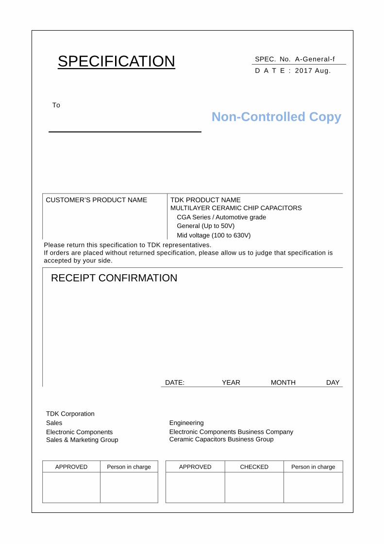
SPECIFICATION SPEC. No. A-General-f
D A T E : 2017 Aug.
To
Upon the acceptance of this spec.
previous spec. (C2005-1420)
shall be abolished.
CUSTOMER’S PRODUCT NAME TDK PRODUCT NAME MULTILAYER CERAMIC CHIP CAPACITORS
CGA Series / Automotive grade General (Up to 50V)
Mid voltage (100 to 630V)
Please return this specification to TDK representatives. If orders are placed without returned specification, please allow us to judge that specification is accepted by your side.
RECEIPT CONFIRMATION
DATE: YEAR MONTH DAY
TDK Corporation
Sales Engineering
Electronic Components Sales & Marketing Group
Electronic Components Business Company Ceramic Capacitors Business Group
APPROVED Person in charge APPROVED CHECKED Person in charge
Non-Controlled Copy
— 1 —
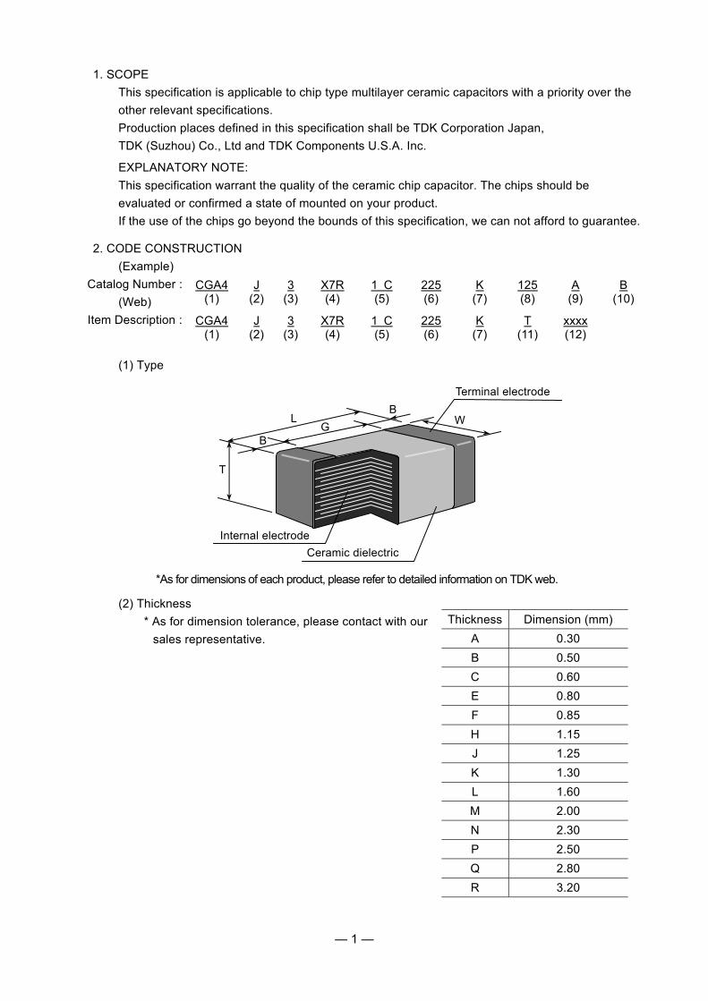
1. SCOPE
This specification is applicable to chip type multilayer ceramic capacitors with a priority over the
other relevant specifications.
Production places defined in this specification shall be TDK Corporation Japan,
TDK (Suzhou) Co., Ltd and TDK Components U.S.A. Inc.
EXPLANATORY NOTE:
This specification warrant the quality of the ceramic chip capacitor. The chips should be
evaluated or confirmed a state of mounted on your product.
If the use of the chips go beyond the bounds of this specification, we can not afford to guarantee.
2. CODE CONSTRUCTION
(Example)
Catalog Number : CGA4 J 3 X7R 1 C 225 K 125 A B
(Web) (1) (2) (3) (4) (5) (6) (7) (8) (9) (10)
Item Description : CGA4 J 3 X7R 1 C 225 K T xxxx
(1) (2) (3) (4) (5) (6) (7) (11) (12)
(1) Type
*As for dimensions of each product, please refer to detailed information on TDK web.
(2) Thickness
* As for dimension tolerance, please contact with our
sales representative.
Thickness Dimension (mm)
A 0.30
B 0.50
C 0.60
E 0.80
F 0.85
H 1.15
J 1.25
K 1.30
L 1.60
M 2.00
N 2.30
P 2.50
Q 2.80
R 3.20
L
B G
BW
T
Terminal electrode
Ceramic dielectric
Internal electrode

— 2 —
(3) Voltage condition in the life test
(Max. operating Temp./1000h)
Sign Condition
1 Rated Voltage x 1
2 Rated Voltage x 2
3 Rated Voltage x 1.5
4 Rated Voltage x 1.2
(4) Temperature Characteristics (Details are shown in table 1 No.7 at page 4 and No.8 at page 5)
(5) Rated Voltage
Symbol Rated Voltage
2 J DC 630 V
2 W DC 450 V
2 E DC 250 V
2 A DC 100 V
1 H DC 50 V
1 V DC 35 V
1 E DC 25 V
1 C DC 16 V
1 A DC 10 V
0 J DC 6.3 V
(6) Rated Capacitance
Stated in three digits and in units of pico farads (pF).
The first and Second digits identify the first and second significant figures of the capacitance,
the third digit identifies the multiplier.
R is designated for a decimal point.
Example 2R2 → 2.2pF
225 → 2,200,000pF
(7) Capacitance tolerance Symbol Tolerance Capacitance
C ± 0.25 pF 10pF and under
D ± 0.5 pF
J ± 5 %
Over 10pF
K ± 10 %
M ± 20 %
(8) Thickness code (Only Catalog Number)
(9) Package code (Only Catalog Number)
(10) Special code (Only Catalog Number)
(11) Packaging (Only Item Description)
(Bulk is not applicable for CGA1 and CGA2 type.)
Symbol Packaging
B Bulk
T Taping
(12) Internal code (Only Item Description)

— 3 —
3. RATED CAPACITANCE AND TOLERANCE
3.1 Standard combination of rated capacitance and tolerances
Class
Temperature Characteristics
Capacitance tolerance Rated capacitance
1 C0G
10pF and under
C (±0.25pF) 1, 1.5, 2, 2.2, 3, 3.3, 4, 4.7, 5
D (±0.5pF) 6, 6.8, 7, 8, 9, 10
12pF to 10,000pF
J (±5 %) E – 12 series
Over 10,000pF
E – 6 series
2
X5R X7R X7S X7T
10uF and under
K (±10 %)
M (±20 %) E – 6 series
Over 10uF M (±20 %)
3.2 Capacitance Step in E series E series Capacitance Step
E- 6 1.0 1.5 2.2 3.3 4.7 6.8
E-12 1.0 1.2 1.5 1.8 2.2 2.7 3.3 3.9 4.7 5.6 6.8 8.2
4. OPERATING TEMPERATURE RANGE
T.C. Min. operating Temperature
Max. operating Temperature
Reference Temperature
X5R -55°C 85°C 25°C
C0G X7R X7S X7T
-55°C 125°C 25°C
5. STORING CONDITION AND TERM
5 to 40°C at 20 to 70%RH 6 months Max.
6. P.C. BOARD
When mounting on an aluminum substrate, large case sizes such as CGA6, CGA8 and CGA9 types are more likely to be affected by heat stress from the substrate. Please inquire separate specification for the large case sizes when mounted on the substrate.
7. INDUSTRIAL WASTE DISPOSAL Dispose this product as industrial waste in accordance with the Industrial Waste Law.

— 4 —
8. PERFORMANCE table 1
No. Item Performance Test or inspection method
1 External Appearance
No defects which may affect performance.
Inspect with magnifying glass (3×), in case
of CGA1 type, with magnifying glass (10×)
2 Insulation Resistance
10,000MΩ or 500MΩ·μF min.(As for the capacitors of rated voltage 16V DC and the item below, 10,000 MΩ or 100MΩ·μF min.,) whichever smaller.
Apply rated voltage for 60s. As for the rated voltage 630V DC, apply 500V.
3 Voltage Proof Withstand test voltage without insulation breakdown or other damage.
ClassRated
voltage(RV) Apply voltage
1
RV≦100V 3 × rated voltage
100V<RV≦500V 1.5 × rated voltage
500V<RV 1.3 × rated voltage
2
RV≦100V 2.5 × rated voltage
100V<RV≦500V 1.5 × rated voltage
500V<RV 1.3 × rated voltage
Above DC voltage shall be applied for 1s.Charge / discharge current shall not exceed 50mA.
4 Capacitance Within the specified tolerance. Class Capacitance
Measuringfrequency
Measuring voltage
Class1
1000pF and under
1MHz±10%0.5 - 5 Vrms.
Over 1000pF 1kHz±10%
Class2
10uF and under
1kHz±10%1.0±0.2Vrm s
0.5±0.2Vrms.
Over 10uF 120Hz±20% 0.5±0.2Vrms.
5 Q (Class1)
See No.4 in this table for measuring condition. Capacitance Q
30pF and over 1,000 min.
Under 30pF 400+20×C min.
C : Rated capacitance (pF)
6 Dissipation Factor (Class2)
0.025 max. 0.03 max. 0.05 max. 0.075 max. 0.1 max.
See No.4 in this table for measuring condition. For information which product has which dissipation factor, please see the detail page of each product on website.
7 Temperature Characteristics of Capacitance (Class1)
Temperature coefficient shall be calculated based on values at 25°C and 85°C temperature. Measuring temperature below 20°C shall be -10°C and -25°C.
T.C. Temperature Coefficient
C0G 0 ± 30 (ppm/°C)
Capacitance drift within ± 0.2% or
± 0.05pF, whichever larger.

— 5 —
(continued)
No. Item Performance Test or inspection method
8
Temperature Characteristics of Capacitance (Class2)
Capacitance Change (%) Capacitance shall be measured by the steps shown in the following table after thermal equilibrium is obtained for each step. ∆C be calculated ref. STEP3 reading
No voltage applied
X5R : ± 15 X7R : ± 15 X7S : ± 22 Step Temperature(°C)
X7T : +22, -33 1 Reference temp. ± 2
2 Min. operating temp. ± 3
3 Reference temp. ± 2
4 Max. operating temp. ± 2
Measuring voltage : 0.1, 0.2, 0.5, 1.0Vrms.For information which product has which Measuring voltage, please contact with our sales representative.
9 Robustness of Terminations
No sign of termination coming off, breakage of ceramic, or other abnormal signs.
Reflow solder the capacitors on a P.C.Board shown in Appendix 1a or Appendix 1b and apply a pushing force of 17.7N with 10±1s. (2N is applied for CGA1, CGA2 type)
10 Bending No mechanical damage. Reflow solder the capacitors on a P.C.Board shown in Appendix 2a or Appendix 2b and bend it for 2mm. (1mm is applied for 0.85mm thickness of Class2 items.)
(Unit : mm)
Pushing force
P.C.Board Capacitor
2
20
50 F
R230
45 45

— 6 —
(continued)
No. Item Performance Test or inspection method
11 Solderability New solder to cover over 75% of termination. 25% may have pin holes or rough spots but not concentrated in one spot. Ceramic surface of A sections shall not be exposed due to melting or shifting of termination material.
Completely soak both terminations in
solder at the following conditions.
Solder : Sn-3.0Ag-0.5Cu or Sn-37Pb
Temperature:245±5°C(Sn-3.0Ag-0.5Cu)
235±5°C(Sn-37Pb) Soaking time:3±0.3s(Sn-3.0Ag-0.5Cu)
2±0.2s(Sn-37Pb)
Flux: Isopropyl alcohol (JIS K 8839)
Rosin (JIS K 5902) 25% solid
solution.
12 Resistance to solder heat
External appearance
No cracks are allowed and terminations shall be covered at least 60% with new solder.
Completely soak both terminations in
solder at the following conditions.
260±5°C for 10±1s.
Preheating condition
Temp. : 110 to 140°C
Time : 30 to 60s.
Solder : Sn-3.0Ag-0.5Cu or Sn-37Pb
Flux : Isopropyl alcohol (JIS K 8839)
Rosin (JIS K 5902) 25% solid
solution.
Leave the capacitors in ambient
condition for 6 to 24h (Class1) or 24±2h
(Class2) before measurement.
Capacitance
Characteristics
Change from the value before test
Class1 C0G
Capacitance drift within ± 2.5% or ± 0.25pF, whichever larger.
Class2
X5RX7RX7SX7T
± 7.5 %
Q (Class1)
Meet the initial spec.
D.F. (Class2)
Meet the initial spec.
Insulation Resistance
Meet the initial spec.
Voltage proof
No insulation breakdown or other damage.
A section
— 7 —
(continued)
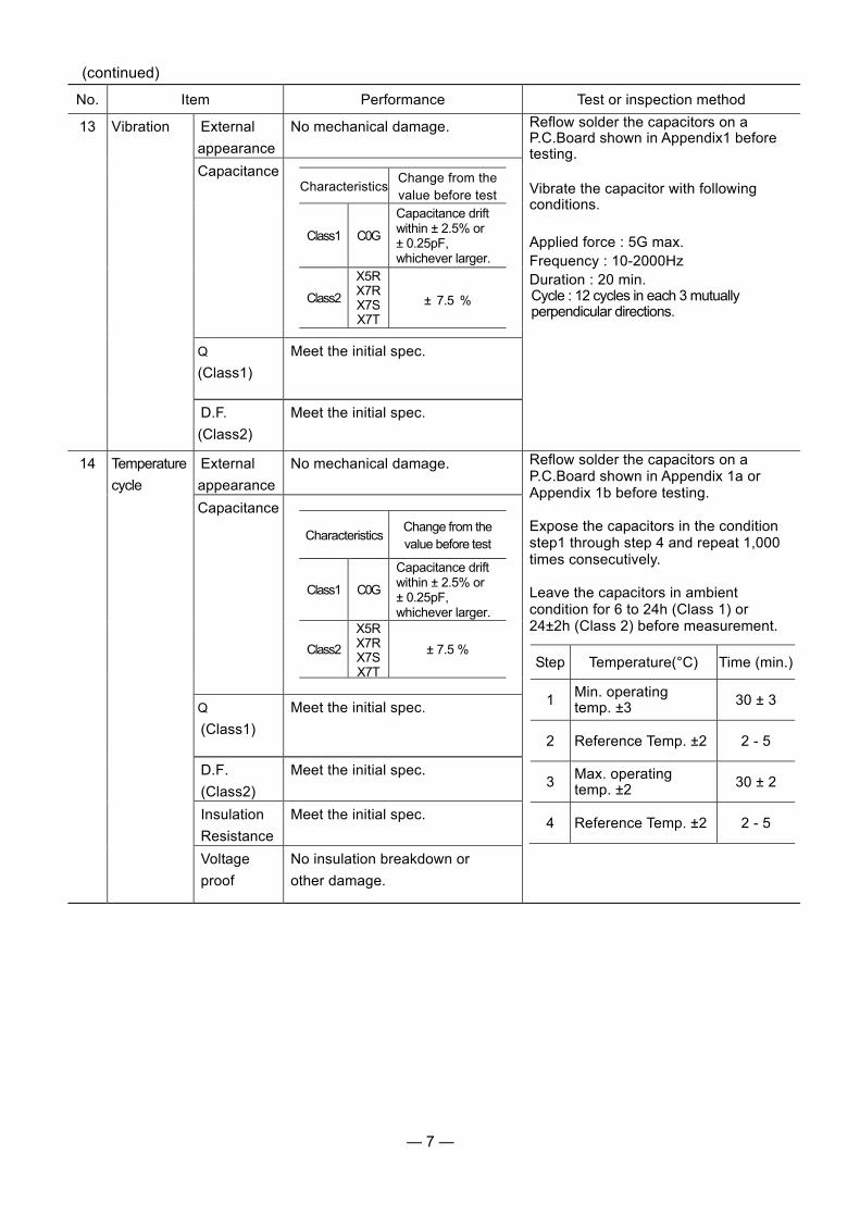
No. Item Performance Test or inspection method
13 Vibration External
appearance
No mechanical damage. Reflow solder the capacitors on a P.C.Board shown in Appendix1 before testing. Vibrate the capacitor with following conditions. Applied force : 5G max. Frequency : 10-2000Hz Duration : 20 min. Cycle : 12 cycles in each 3 mutually perpendicular directions.
Capacitance Characteristics
Change from the value before test
Class1 C0G
Capacitance drift within ± 2.5% or ± 0.25pF, whichever larger.
Class2
X5RX7RX7SX7T
± 7.5 %
Q
(Class1)
Meet the initial spec.
D.F.
(Class2)
Meet the initial spec.
14 Temperature
cycle
External
appearance
No mechanical damage. Reflow solder the capacitors on a P.C.Board shown in Appendix 1a or Appendix 1b before testing. Expose the capacitors in the condition step1 through step 4 and repeat 1,000 times consecutively. Leave the capacitors in ambient condition for 6 to 24h (Class 1) or 24±2h (Class 2) before measurement.
Capacitance
Characteristics
Change from the value before test
Class1 C0G
Capacitance drift within ± 2.5% or ± 0.25pF, whichever larger.
Class2
X5RX7RX7SX7T
± 7.5 %
Q
(Class1)
Meet the initial spec.
D.F.
(Class2)
Meet the initial spec.
Insulation
Resistance
Meet the initial spec.
Voltage
proof
No insulation breakdown or
other damage.
Step Temperature(°C) Time (min.)
1 Min. operating temp. ±3 30 ± 3
2 Reference Temp. ±2 2 - 5
3 Max. operating temp. ±2 30 ± 2
4 Reference Temp. ±2 2 - 5
— 8 —
(continued)
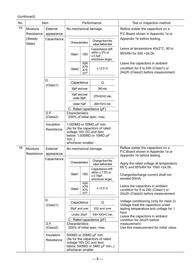
No. Item Performance Test or inspection method
15 Moisture
Resistance
(Steady
State)
External
appearance
No mechanical damage. Reflow solder the capacitors on a
P.C.Board shown in Appendix 1a or
Appendix 1b before testing.
Leave at temperature 40±2°C, 90 to
95%RH for 500 +24,0h.
Leave the capacitors in ambient
condition for 6 to 24h (Class1) or 24±2h (Class2) before measurement.
Capacitance
CharacteristicsChange from the value before test
Class1 C0G
Capacitance drift within ± 5% or ± 0.5pF, whichever larger.
Class2
X5RX7RX7SX7T
± 12.5 %
Q
(Class1)
Capacitance Q
30pF and over 350 min.
10pF and over under 30pF
275+5/2×C min.
Under 10pF 200+10×C min.
C : Rated capacitance (pF) D.F. (Class2)
Characteristics 200% of initial spec. max.
Insulation
Resistance
1,000MΩ or 50MΩ·μF min. (As for the capacitors of rated voltage 16V DC and item below, 1,000MΩ or 10MΩ·μF min.,) whichever smaller.
16 Moisture
Resistance
External
appearance
No mechanical damage. Reflow solder the capacitors on a P.C.Board shown in Appendix 1a or Appendix 1b before testing. Apply the rated voltage at temperature 85°C and 85%RH for 1000 +24,0h. Charge/discharge current shall not exceed 50mA. Leave the capacitors in ambient condition for 6 to 24h (Class1) or 24±2h (Class2) before measurement. Voltage conditioning (only for class 2) Voltage treat the capacitors under testing temperature and voltage for 1 hour. Leave the capacitors in ambient condition for 24±2h before measurement. Use this measurement for initial value.
Capacitance Characteristics
Change from the value before test
Class1 C0G
Capacitance drift within ± 7.5% or ± 0.75pF, whichever larger.
Class2
X5RX7RX7SX7T
± 12.5 %
Q
(Class1)
Capacitance Q
30pF and over 200 and over
Under 30pF 100+10/3×C min.
C : Rated capacitance (pF) D.F. (Class2)
Characteristics 200% of initial spec. max.
Insulation
Resistance
500MΩ or 25MΩ·μF min. (As for the capacitors of rated voltage 16V DC and item below, 500MΩ or 5MΩ·μF min.,) whichever smaller.

— 9 —
(continued)
No. Item Performance Test or inspection method
17 Life External
appearance
No mechanical damage. Reflow solder the capacitors on a P.C.Board shown in Appendix 1a or Appendix 1b before testing. Below the voltage shall be applied at maximum operating temperature ±2°C for 1,000 +48, 0h.
For information which product has which applied voltage, please contact with our sales representative. Charge/discharge current shall not exceed 50mA. Leave the capacitors in ambient condition for 6 to 24h (Class1) or 24±2h (Class2) before measurement. Voltage conditioning (only for class 2) Voltage treat the capacitors under testing temperature and voltage for 1 hour. Leave the capacitors in ambient condition for 24±2h before measurement. Use this measurement for initial value.
Capacitance Characteristics
Change from the value before test
Class1 C0G
Capacitance drift within ± 3% or ± 0.3pF, whichever larger.
Class2
X5RX7RX7SX7T
± 15 %
Q
(Class1)
Capacitance Q
30pF and over 350 and over
10pF and over to under 30pF
275+5/2×C min.
Under 10pF 200+10×C min.
C : Rated capacitance (pF) D.F. (Class2)
Characteristics 200% of initial spec. max.
Insulation
Resistance
1,000MΩ or 50MΩ·μF min. (As for the capacitors of rated voltage 16V DC and the item
below, 1,000 MΩ or 10MΩ·μF min.,) whichever smaller.
*As for the initial measurement of capacitors (Class2) on number 8,12,13,14 and 15 leave capacitors at
150 –10,0°C for 1 hour and measure the value after leaving capacitors for 24±2h in ambient condition.
Applied voltage
Rated voltage x2
Rated voltage x1.5
Rated voltage x1.2
Rated voltage x1
— 10 —
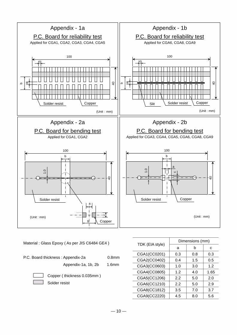
TDK (EIA style) Dimensions (mm)
a b c
CGA1(CC0201) 0.3 0.8 0.3
CGA2(CC0402) 0.4 1.5 0.5
CGA3(CC0603) 1.0 3.0 1.2
CGA4(CC0805) 1.2 4.0 1.65
CGA5(CC1206) 2.2 5.0 2.0
CGA6(CC1210) 2.2 5.0 2.9
CGA8(CC1812) 3.5 7.0 3.7
CGA9(CC2220) 4.5 8.0 5.6
Appendix - 2a
P.C. Board for bending test Applied for CGA1, CGA2
1.0
c
40
a
b
100
Copper
Solder resist
Appendix - 2b
P.C. Board for bending test Applied for CGA3, CGA4, CGA5, CGA6, CGA8, CGA9
1.0
c
40
a
b
100
Copper Solder resist
Appendix - 1a
P.C. Board for reliability test Applied for CGA1, CGA2, CGA3, CGA4, CGA5
100
c
a b 40
Copper Solder resist
(Unit:mm)
Appendix - 1b
P.C. Board for reliability test Applied for CGA6, CGA8, CGA9
100
c
a b 40
Copper Solder resist Slit
(Unit : mm)
(Unit : mm) (Unit : mm)
b
Material : Glass Epoxy ( As per JIS C6484 GE4 )
P.C. Board thickness : Appendix-2a 0.8mm
Appendix-1a, 1b, 2b 1.6mm
Copper ( thickness 0.035mm )
Solder resist
— 11 —
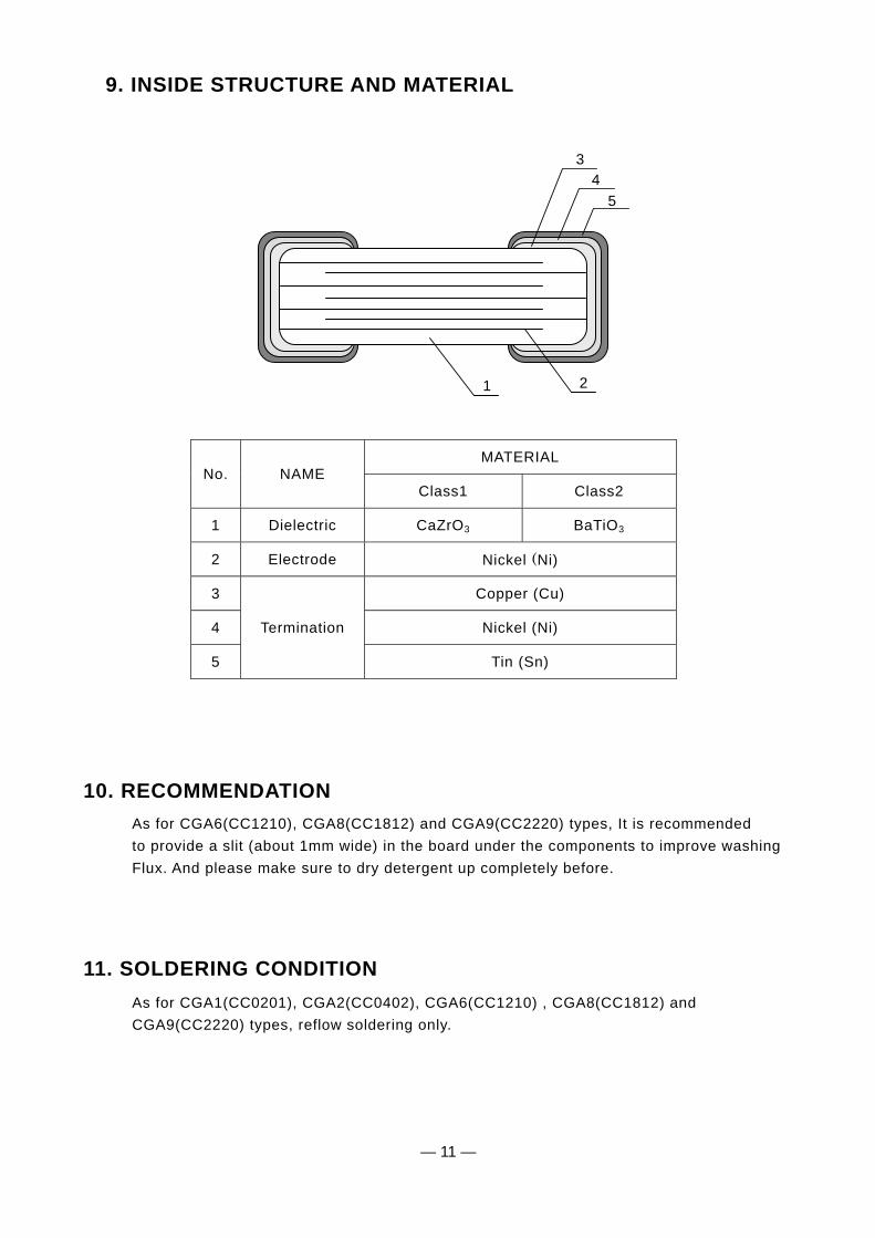
9. INSIDE STRUCTURE AND MATERIAL
No. NAME MATERIAL
Class1 Class2
1 Dielectric CaZrO3 BaTiO3
2 Electrode Nickel (Ni)
3
Termination
Copper (Cu)
4 Nickel (Ni)
5 Tin (Sn)
10. RECOMMENDATION
As for CGA6(CC1210), CGA8(CC1812) and CGA9(CC2220) types, It is recommended
to provide a slit (about 1mm wide) in the board under the components to improve washing
Flux. And please make sure to dry detergent up completely before.
11. SOLDERING CONDITION
As for CGA1(CC0201), CGA2(CC0402), CGA6(CC1210) , CGA8(CC1812) and
CGA9(CC2220) types, reflow soldering only.
3
4
5
1 2

― 12 ―
12. CAUTION No. Process Condition
1 Operating
Condition
(Storage, Transportation)
1-1. Storage 1)
2)
3)
4)
5)
The capacitors must be stored in an ambient temperature of 5 to 40 with a relative humidity of 20 to 70%RH. The products should be used within 6 months upon receipt.
The capacitors must be operated and stored in an environment free of dew condensation and these gases such as Hydrogen Sulphide, Hydrogen Sulphate, Chlorine, Ammonia and sulfur.
Avoid storing in sun light and falling of dew.
Do not use capacitors under high humidity and high and low atmospheric pressure which may affect capacitors reliability.
Capacitors should be tested for the solderability when they are stored for long time.
1-2. Handling in transportation
In case of the transportation of the capacitors, the performance of the capacitors may be deteriorated depending on the transportation condition. (Refer to JEITA RCR-2335C 9.2 Handling in transportation)
2 Circuit design
Caution
2-1. Operating temperatureOperating temperature should be followed strictly within this specification, especially be careful with maximum temperature.
1)
2)
3)
Do not use capacitors above the maximum allowable operating temperature.
Surface temperature including self heating should be below maximum operating temperature. (Due to dielectric loss, capacitors will heat itself when AC is applied. Especially at high frequencies around its SRF, the heat might be so extreme that it may damage itself or the product mounted on. Please design the circuit so that the maximum temperature of the capacitors including the self heating to be below the maximum allowable operating temperature. Temperature rise at capacitor surface shall be below 20)
The electrical characteristics of the capacitors will vary depending on the temperature. The capacitors should be selected and designed in taking the temperature into consideration.
2-2 Operating voltage1) Operating voltage across the terminals should be below the rated voltage.
When AC and DC are super imposed, V0-P must be below the rated voltage. ——— (1) and (2)
AC or pulse with overshooting, VP-P must be below the rated voltage. ——— (3), (4) and (5)
When the voltage is started to apply to the circuit or it is stopped applying, the irregular voltage may be generated for a transit period because of resonance or switching. Be sure to use the capacitors within rated voltage containing these Irregular voltage.
Voltage (1) DC voltage (2) DC+AC voltage (3) AC voltage
Positional Measurement
(Rated voltage)
V0-P
0
V0-P
0
VP-P
Voltage (4) Pulse voltage (A) (5) Pulse voltage (B)
Positional Measurement
(Rated voltage)
VP-P
VP-P
!
0
0
0
― 13 ―
No. Process Condition
2 Circuit design
Caution
2)
3)
Even below the rated voltage, if repetitive high frequency AC or pulse is applied,
the reliability of the capacitors may be reduced.
The effective capacitance will vary depending on applied DC and AC voltages.
The capacitors should be selected and designed in taking the voltages into
consideration.
2-3. Frequency
When the capacitors (Class 2) are used in AC and/or pulse voltages, the
capacitors may vibrate themselves and generate audible sound.
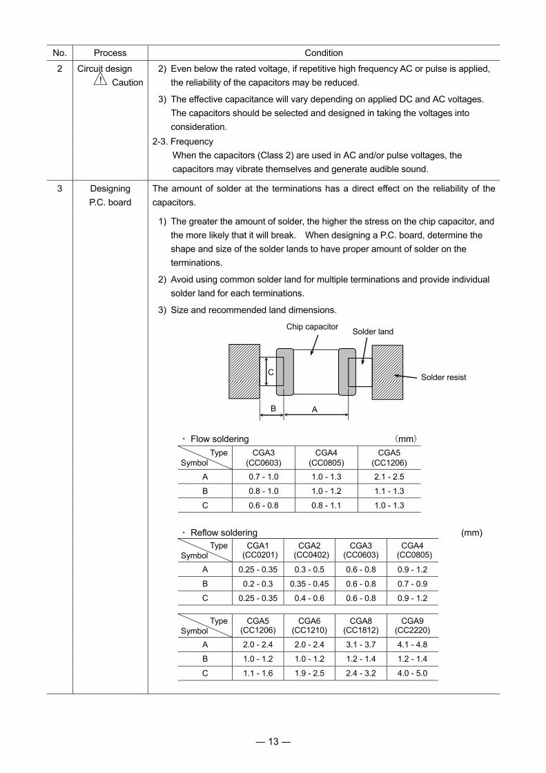
3 Designing
P.C. board
The amount of solder at the terminations has a direct effect on the reliability of the
capacitors.
1)
2)
3)
The greater the amount of solder, the higher the stress on the chip capacitor, and
the more likely that it will break. When designing a P.C. board, determine the
shape and size of the solder lands to have proper amount of solder on the
terminations.
Avoid using common solder land for multiple terminations and provide individual
solder land for each terminations.
Size and recommended land dimensions.
・ Flow soldering (mm)
TypeSymbol
CGA3 (CC0603)
CGA4 (CC0805)
CGA5 (CC1206)
A 0.7 - 1.0 1.0 - 1.3 2.1 - 2.5
B 0.8 - 1.0 1.0 - 1.2 1.1 - 1.3
C 0.6 - 0.8 0.8 - 1.1 1.0 - 1.3
・ Reflow soldering (mm)
TypeSymbol
CGA1 (CC0201)
CGA2 (CC0402)
CGA3 (CC0603)
CGA4 (CC0805)
A 0.25 - 0.35 0.3 - 0.5 0.6 - 0.8 0.9 - 1.2
B 0.2 - 0.3 0.35 - 0.45 0.6 - 0.8 0.7 - 0.9
C 0.25 - 0.35 0.4 - 0.6 0.6 - 0.8 0.9 - 1.2 Type
Symbol CGA5
(CC1206)CGA6
(CC1210)CGA8
(CC1812)CGA9
(CC2220)
A 2.0 - 2.4 2.0 - 2.4 3.1 - 3.7 4.1 - 4.8
B 1.0 - 1.2 1.0 - 1.2 1.2 - 1.4 1.2 - 1.4
C 1.1 - 1.6 1.9 - 2.5 2.4 - 3.2 4.0 - 5.0
!
AB
C
Chip capacitorSolder land
Solder resist

― 14 ―
No. Process Condition
3 Designing
P.C.board
4) Recommended chip capacitor layout is as following.
Disadvantage against bending stress
Advantage against bending stress
Mounting face
Perforation or slit
Break P.C.board with
mounted side up.
Perforation or slit
Break P.C.board with
mounted side down.
Chip arrangement (Direction)
Mount perpendicularly to
perforation or slit
Perforation or slit
Mount in parallel with
perforation or slit
Perforation or slit
Distance from slit
Closer to slit is higher
stress
1
(1 < 2 )
Away from slit is less
stress
2
(1 < 2 )
― 15 ―
No. Process Condition
3 Designing
P.C.board
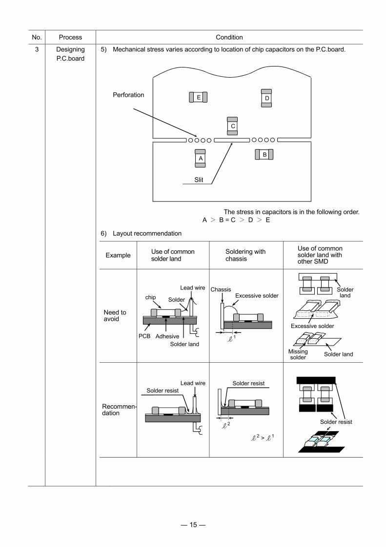
5) Mechanical stress varies according to location of chip capacitors on the P.C.board.
Perforation
The stress in capacitors is in the following order.
A > B = C > D > E
6) Layout recommendation
Example
Use of common solder land
Soldering with chassis
Use of common solder land with other SMD
Need to avoid
Recommen-dation
A
C
D
B
E
Slit
Solder resist
2 > 1
2
Chassis
1
Excessive solder Solder land
Excessive solder
Missing solder Solder land
Lead wireSolder resist
Solder resist
Lead wire
Solderchip
Solder landAdhesivePCB
― 16 ―
No. Process Condition
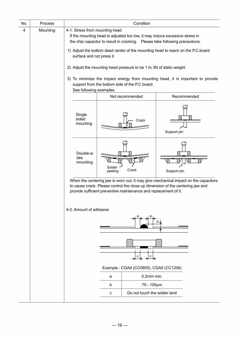
4 Mounting 4-1. Stress from mounting head
If the mounting head is adjusted too low, it may induce excessive stress in
the chip capacitor to result in cracking. Please take following precautions.
1)
2)
3)
Adjust the bottom dead center of the mounting head to reach on the P.C.board
surface and not press it.
Adjust the mounting head pressure to be 1 to 3N of static weight.
To minimize the impact energy from mounting head, it is important to provide
support from the bottom side of the P.C.board.
See following examples.
Not recommended Recommended
Single sided mounting
Double-sides mounting
When the centering jaw is worn out, it may give mechanical impact on the capacitorsto cause crack. Please control the close up dimension of the centering jaw and provide sufficient preventive maintenance and replacement of it.
4-2. Amount of adhesive
Example : CGA4 (CC0805), CGA5 (CC1206)
a 0.2mm min.
b 70 - 100μm
c Do not touch the solder land
a a
b
c c
Crack
Solderpeeling Crack
Support pin
Support pin
― 17 ―
No. Process Condition
5 Soldering 5-1. Flux selection
Although highly-activated flux gives better solderability, substances which increase
activity may also degrade the insulation of the chip capacitors.
To avoid such degradation, it is recommended following.
1)
2)
3)
It is recommended to use a mildly activated rosin flux (less than 0.1wt% chlorine).
Strong flux is not recommended.
Excessive flux must be avoided. Please provide proper amount of flux.
When water-soluble flux is used, enough washing is necessary.
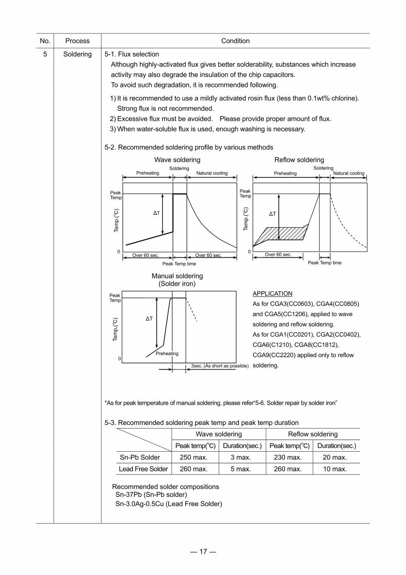
5-2. Recommended soldering profile by various methods
Wave soldering Reflow soldering
Manual soldering (Solder iron)
APPLICATION
As for CGA3(CC0603), CGA4(CC0805)
and CGA5(CC1206), applied to wave
soldering and reflow soldering.
As for CGA1(CC0201), CGA2(CC0402),
CGA6(C1210), CGA8(CC1812),
CGA9(CC2220) applied only to reflow
soldering.
*As for peak temperature of manual soldering, please refer“5-6. Solder repair by solder iron”
5-3. Recommended soldering peak temp and peak temp duration
Wave soldering Reflow soldering
Peak temp() Duration(sec.) Peak temp() Duration(sec.)
Sn-Pb Solder 250 max. 3 max. 230 max. 20 max.
Lead Free Solder 260 max. 5 max. 260 max. 10 max.
Recommended solder compositions Sn-37Pb (Sn-Pb solder) Sn-3.0Ag-0.5Cu (Lead Free Solder)
PeakTemp
0
∆T
Preheating Soldering
Natural cooling
Over 60 sec. Over 60 sec.
Peak Temp time
Tem
p.(
)
0
∆T
3sec. (As short as possible)
Preheating
Tem
p..(
)
PeakTemp
∆T
Preheating Soldering
Natural cooling
Over 60 sec. 0
Peak Temp time
PeakTemp
Tem
p.(
)

― 18 ―
No. Process Condition
5 Soldering 5-4. Avoiding thermal shock
1) Preheating condition
Soldering Type Temp. ()
Wave soldering
CGA3(CC0603), CGA4(CC0805), CGA5(CC1206)
∆T ≤150
Reflow soldering
CGA1(CC0201), CGA2(CC0402), CGA3(CC0603), CGA4(CC0805), CGA5(CC1206)
∆T ≤150
CGA6(CC1210), CGA8(CC1812), CCGA9(CC2220)
∆T ≤130
Manual soldering
CGA1(CC0201), CGA2(CC0402), CGA3(CC0603), CGA4(CC0805), CGA5(CC1206)
∆T ≤150
CGA6(CC1210), CGA8(CC1812), CGA9(CC2220)
∆T ≤130
2) Cooling condition
Natural cooling using air is recommended. If the chips are dipped into a solvent for cleaning, the temperature difference (∆T) must be less than 100.
5-5. Amount of solderExcessive solder will induce higher tensile force in chip capacitors when temperature changes and it may result in chip cracking. In sufficient solder may detach the capacitors from the P.C.board.
Excessive solder
Higher tensile force in chip capacitor to cause crack
Adequate
Insufficient solder
Low robustness may cause contact failure or chip capacitor comes off the P.C.board.
5-6. Solder repair by solder iron
1) Selection of the soldering iron tipTip temperature of solder iron varies by its type, P.C.board material and solder land size. The higher the tip temperature, the quicker the operation. However, heat shock may cause a crack in the chip capacitors. Please make sure the tip temp. before soldering and keep the peak temp and time in accordance with following recommended condition. (Please preheat the chip capacitors with the condition in 5-4 to avoid the thermal shock.) Recommended solder iron condition (Sn-Pb Solder and Lead Free Solder)
Type Temp. (°C) Wattage (W) Shape (mm)
CGA1(CC0201) CGA2(CC0402) CGA3(CC0603) CGA4(CC0805) CGA5(CC1206)
350 max.
20 max. φ3.0 max.
CGA6(CC1210) CGA8(CC1812) CGA9(CC2220)
280 max.
Maximum amount Minimum amount
― 19 ―
No. Process Condition
5 Soldering 2)
3)
Direct contact of the soldering iron with ceramic dielectric of chip capacitors may cause crack. Do not touch the ceramic dielectric and the terminations by solder iron. It is not recommended to reuse dismounted capacitors. (For soft electrode)
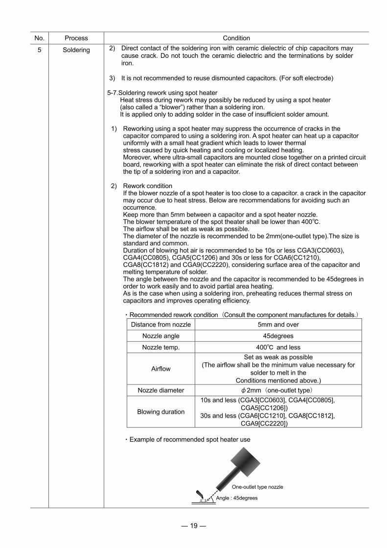
5-7.Soldering rework using spot heater Heat stress during rework may possibly be reduced by using a spot heater
(also called a “blower”) rather than a soldering iron. It is applied only to adding solder in the case of insufficient solder amount.
1)
2)
Reworking using a spot heater may suppress the occurrence of cracks in the capacitor compared to using a soldering iron. A spot heater can heat up a capacitor uniformly with a small heat gradient which leads to lower thermal stress caused by quick heating and cooling or localized heating. Moreover, where ultra-small capacitors are mounted close together on a printed circuit board, reworking with a spot heater can eliminate the risk of direct contact between the tip of a soldering iron and a capacitor. Rework condition If the blower nozzle of a spot heater is too close to a capacitor. a crack in the capacitor may occur due to heat stress. Below are recommendations for avoiding such an occurrence. Keep more than 5mm between a capacitor and a spot heater nozzle. The blower temperature of the spot theater shall be lower than 400. The airflow shall be set as weak as possible. The diameter of the nozzle is recommended to be 2mm(one-outlet type).The size is standard and common. Duration of blowing hot air is recommended to be 10s or less CGA3(CC0603), CGA4(CC0805), CGA5(CC1206) and 30s or less for CGA6(CC1210), CGA8(CC1812) and CGA9(CC2220), considering surface area of the capacitor and melting temperature of solder. The angle between the nozzle and the capacitor is recommended to be 45degrees in order to work easily and to avoid partial area heating. As is the case when using a soldering iron, preheating reduces thermal stress on capacitors and improves operating efficiency. ・Recommended rework condition(Consult the component manufactures for details.)
Distance from nozzle 5mm and over
Nozzle angle 45degrees
Nozzle temp. 400 and less
Airflow
Set as weak as possible (The airflow shall be the minimum value necessary for
solder to melt in the Conditions mentioned above.)
Nozzle diameter φ2mm(one-outlet type)
Blowing duration
10s and less (CGA3[CC0603], CGA4[CC0805], CGA5[CC1206])
30s and less (CGA6[CC1210], CGA8[CC1812], CGA9[CC2220])
・Example of recommended spot heater use
One-outlet type nozzle
Angle : 45degrees
― 20 ―
No. Process Condition
5 Soldering 3) Amount of solder should be suitable to from a proper fillet shape. Excess solder causes mechanical and thermal stress on a capacitor and results in cracks. Insufficient solder causes weak adherence of the capacitor to the substrate and may result in detachment of a capacitor and deteriorate reliability of the printed wiring board. See the example of appropriate solder fillet shape for 5-5.Amount of solder.
5-8. Sn-Zn solder
Sn-Zn solder affects product reliability.
Please contact TDK in advance when utilize Sn-Zn solder.
5-9. Countermeasure for tombstone
The misalignment between the mounted positions of the capacitors and the land
patterns should be minimized. The tombstone phenomenon may occur especially
the capacitors are mounted (in longitudinal direction) in the same direction of the
reflow soldering.
(Refer to JEITA RCR-2335C Annex A (Informative) Recommendations to prevent the
tombstone phenomenon)
6 Cleaning 1) 2)
If an unsuitable cleaning fluid is used, flux residue or some foreign articles may stick to chip capacitors surface to deteriorate especially the insulation resistance. If cleaning condition is not suitable, it may damage the chip capacitors.
2)-1. Insufficient washing
(1)
(2)
(3)
Terminal electrodes may corrode by Halogen in the flux. Halogen in the flux may adhere on the surface of capacitors, and lower the insulation resistance. Water soluble flux has higher tendency to have above mentioned problems (1) and (2).
2)-2. Excessive washing
When ultrasonic cleaning is used, excessively high ultrasonic energy output can affect the connection between the ceramic chip capacitor's body and the terminal electrode. To avoid this, following is the recommended condition.
Power : 20W/ max. Frequency : 40kHz max. Washing time : 5 minutes max.
2)-3. If the cleaning fluid is contaminated, density of Halogen increases, and it may
bring the same result as insufficient cleaning.
― 21 ―
No. Process Condition
7 Coating and
molding of the
P.C. board
1)
2)
3)
When the P.C. board is coated, please verify the quality influence on the product. Please verify carefully that there is no harmful decomposing or reaction gas emission during curing which may damage the chip capacitors. Please verify the curing temperature.
8 Handling after
chip mounted
Caution
1)
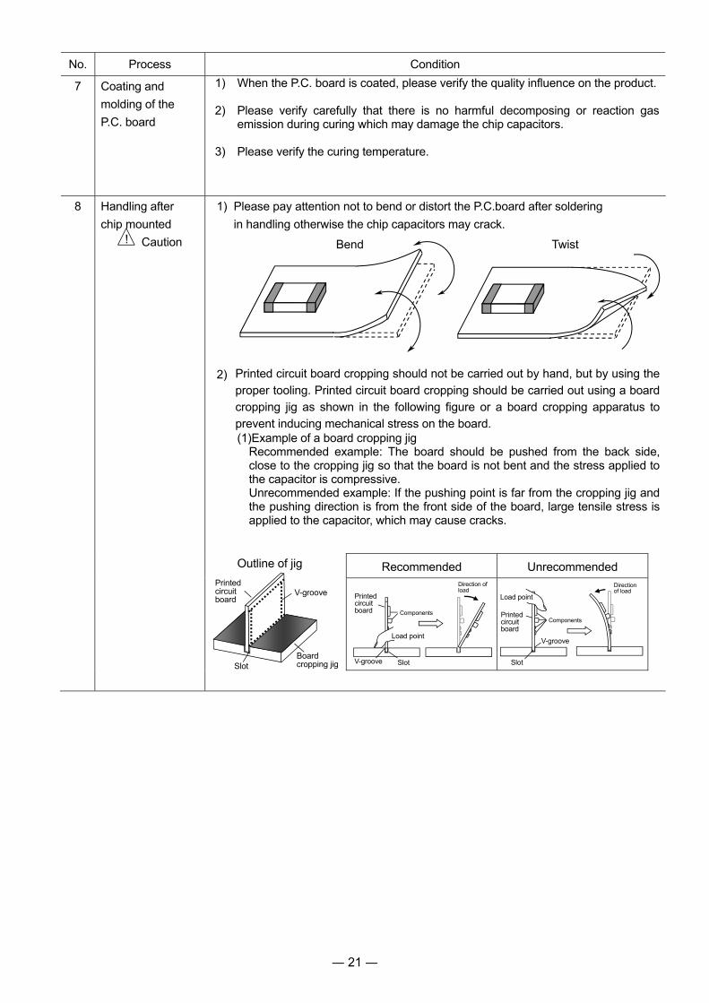
Please pay attention not to bend or distort the P.C.board after soldering
in handling otherwise the chip capacitors may crack.
Bend Twist
2) Printed circuit board cropping should not be carried out by hand, but by using the
proper tooling. Printed circuit board cropping should be carried out using a board
cropping jig as shown in the following figure or a board cropping apparatus to
prevent inducing mechanical stress on the board.
(1)Example of a board cropping jig Recommended example: The board should be pushed from the back side, close to the cropping jig so that the board is not bent and the stress applied to the capacitor is compressive. Unrecommended example: If the pushing point is far from the cropping jig and the pushing direction is from the front side of the board, large tensile stress is applied to the capacitor, which may cause cracks.
Outline of jig Recommended Unrecommended
!
Printed circuit board
V-groove
Boardcropping jig Slot
Printedcircuit board
SlotV-groove
Load point
Components
Direction of load
Direction of load
Components Printed circuit board
Load point
Slot
V-groove
― 22 ―
No. Process Condition
8 Handling after
chip mounted
Caution
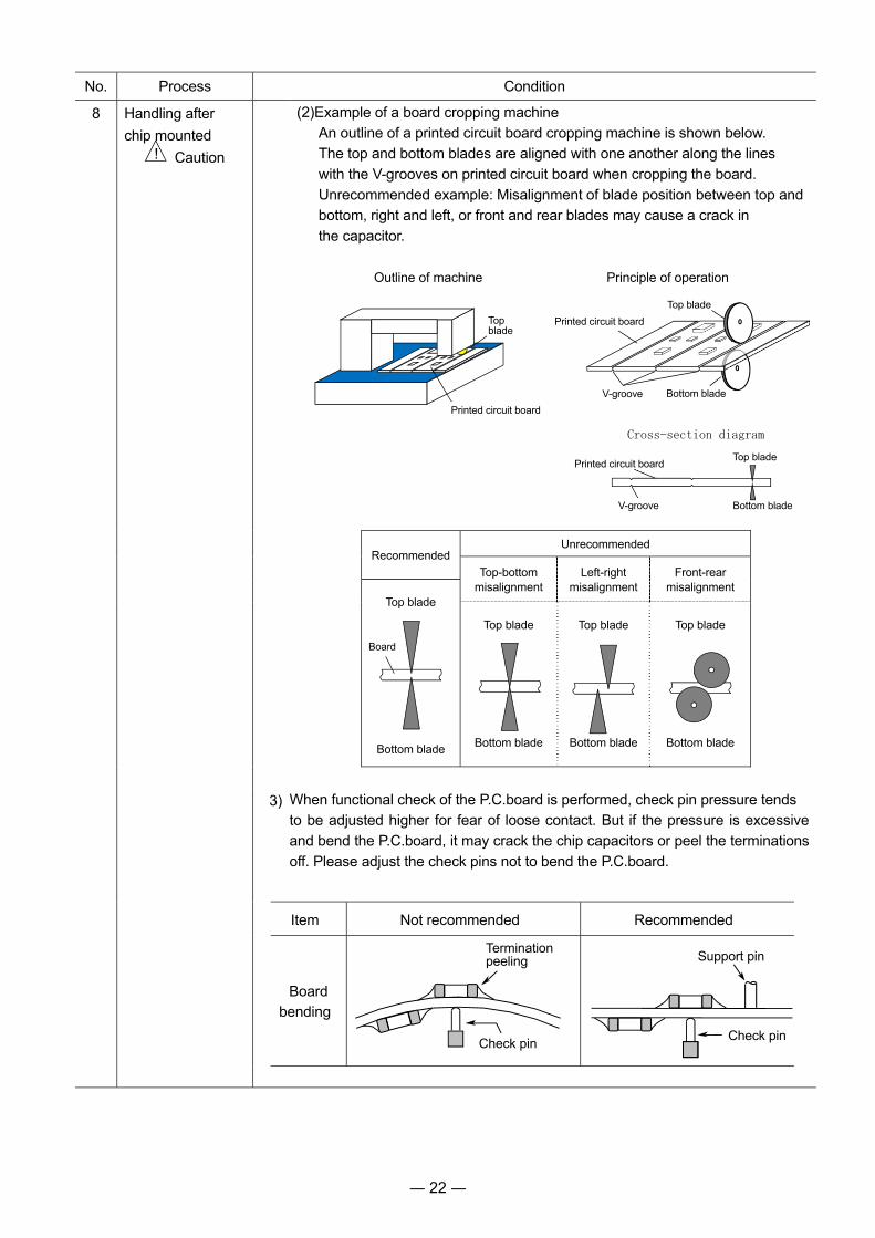
(2)Example of a board cropping machine
An outline of a printed circuit board cropping machine is shown below.
The top and bottom blades are aligned with one another along the lines
with the V-grooves on printed circuit board when cropping the board.
Unrecommended example: Misalignment of blade position between top and
bottom, right and left, or front and rear blades may cause a crack in
the capacitor.
Outline of machine Principle of operation
RecommendedUnrecommended
Top-bottom misalignment
Left-right misalignment
Front-rear misalignment
Top blade
Board
Bottom blade
Top blade
Bottom blade
Top blade
Bottom blade
Top blade
Bottom blade
3) When functional check of the P.C.board is performed, check pin pressure tends
to be adjusted higher for fear of loose contact. But if the pressure is excessive
and bend the P.C.board, it may crack the chip capacitors or peel the terminations
off. Please adjust the check pins not to bend the P.C.board.
Item Not recommended Recommended
Board bending
!
Cross-section diagram
Printed circuit board
V-groove Bottom blade
Top blade
Check pin
Terminationpeeling Support pin
Check pin
Printed circuit board
Top blade
V-groove Bottom blade
Top blade
Printed circuit board

― 23 ―
No. Process Condition
9 Handling of loose
chip capacitors
1) If dropped the chip capacitors may crack. Once dropped do not use it. Especially,
the large case sized chip capacitors are tendency to have cracks easily, so please
handle with care.
2) Piling the P.C.board after mounting for storage or handling, the corner of the P.C. board may hit the chip capacitors of another board to cause crack.
10 Capacitance aging The capacitors (Class 2) have aging in the capacitance. They may not be used in precision time constant circuit. In case of the time constant circuit, the evaluation should be done well.
11 Estimated life and estimated failure rate of capacitors
As per the estimated life and the estimated failure rate depend on the temperature and the voltage. This can be calculated by the equation described in JEITA RCR-2335C Annex F(Informative) Calculation of the estimated lifetime and the estimated failure rate (Voltage acceleration coefficient : 3 multiplication rule, Temperature acceleration coefficient : 10 rule) The failure rate can be decreased by reducing the temperature and the voltage but they will not be guaranteed.
Crack
Floor
P.C.boardCrack
― 24 ―
No. Process Condition
12 Caution during
operation of
equipment
1)
2)
3)
A capacitor shall not be touched directly with bare hands during operation in order to avoid electric shock. Electric energy held by the capacitor may be discharged through the human body when touched with a bare hand. Even when the equipment is off, a capacitor may stay charged. The capacitor should be handled after being completely discharged using a resistor. The terminals of a capacitor shall not be short-circuited by any accidental contact with a conductive object. A capacitor shall not be exposed to a conductive liquid such as an acid or alkali solution. A conductive object or liquid, such as acid and alkali, between the terminals may lead to the breakdown of a capacitor due to short circuit Confirm that the environment to which the equipment will be exposed during transportation and operation meets the specified conditions. Do not to use the equipment in the following environments. (1) Environment where a capacitor is spattered with water or oil (2) Environment where a capacitor is exposed to direct sunlight (3) Environment where a capacitor is exposed to Ozone, ultraviolet rays or
radiation (4) Environment where a capacitor exposed to corrosive gas(e.g. hydrogen sulfide, sulfur dioxide, chlorine. ammonia gas etc.) (5) Environment where a capacitor exposed to vibration or mechanical shock
exceeding the specified limits. (6) Atmosphere change with causes condensation
13 Others
Caution
The products listed on this specification sheet are intended for use in general electronic equipment (AV equipment, telecommunications equipment, home appliances, amusement equipment, computer equipment, personal equipment, office equipment, measurement equipment, industrial robots) under a normal operation and use condition.
The products are not designed or warranted to meet the requirements of the applications listed below, whose performance and/or quality require a more stringent level of safety or reliability, or whose failure, malfunction or trouble could cause serious damage to society, person or property. Please understand that we are not responsible for any damage or liability caused by use of the products in any of the applications below or for any other use exceeding the range or conditions set forth in this specification sheet. If you intend to use the products in the applications listed below or if you have special requirements exceeding the range or conditions set forth in this specification, please contact us.
(1) Aerospace/Aviation equipment (2) Transportation equipment (electric trains, ships, etc.) (3) Medical equipment (Excepting Pharmaceutical Affairs Law classification Class1, 2)(4) Power-generation control equipment (5) Atomic energy-related equipment (6) Seabed equipment (7) Transportation control equipment (8) Public information-processing equipment (9) Military equipment (10) Electric heating apparatus, burning equipment (11) Disaster prevention/crime prevention equipment (12) Safety equipment (13) Other applications that are not considered general-purpose applications
When designing your equipment even for general-purpose applications, you are kindly requested to take into consideration securing protection circuit/device or providing backup circuits in your equipment.
!
— 25 —
13. PACKAGING LABEL
Packaging shall be done to protect the components from the damage during
transportation and storing, and a label which has the following information shall be
attached.
1) Inspection No.
2) TDK P/N
3) Customer's P/N
4) Quantity
*Composition of Inspection No.
Example F 7 A – ΟΟ – ΟΟΟ
(a) (b) (c) (d) (e)
a) Line code
b) Last digit of the year
c) Month and A for January and B for February and so on. (Skip I)
d) Inspection Date of the month.
e) Serial No. of the day
14. BULK PACKAGING QUANTITY
Total number of components in a plastic bag for bulk packaging : 1,000pcs.
As for CGA1, CGA2 types, not available for bulk packaging.

— 26 —
15. TAPE PACKAGING SPECIFICATION
1. CONSTRUCTION AND DIMENSION OF TAPING
1-1. Dimensions of carrier tape Dimensions of paper tape shall be according to Appendix 3, 4, 5. Dimensions of plastic tape shall be according to Appendix 6, 7.
1-2. Bulk part and leader of taping
1-3. Dimensions of reel
Dimensions of Ø178 reel shall be according to Appendix 8, 9. Dimensions of Ø330 reel shall be according to Appendix 10, 11.
1-4. Structure of taping 2. CHIP QUANTITY
Type Thickness
of chip Taping
Material
Chip quantity(pcs.)
Ø 178mm reel Ø 330mm reel
CGA1(CC0201) 0.30 mm Paper 15,000 - CGA2(CC0402) 0.50 mm Paper 10,000 50,000 CGA3(CC0603) 0.80 mm Paper/ Plastic 4,000 10,000
CGA4(CC0805) 0.60mm Paper 4,000 20,000 0.85 mm Paper 10,000 1.25 mm Plastic 2,000
CGA5(CC1206)
0.60 mm Paper 4,000 10,000 0.85 mm
1.15 mmPlastic 2,000 1.30 mm
1.60 mm 8,000
CGA6(CC1210)
1.25 mm
Plastic
2,000 8,000 1.60 mm2.00 mm
1,000 5,000 2.30 mm2.50 mm
CGA8(CC1812)
1.60 mm
Plastic
1,000 3,000 2.00 mm
2.30 mm
500 2.50 mm2.80 mm 2,000 3.20 mm
CGA9(CC2220)
1.60 mm
Plastic
1,000
3,000 2.00 mm500 2.30 mm
2.50 mm
Drawing direction Leader
400mm min
Bulk 160mm
Chips Bulk
160mm min
Paper carrier tape
Pitch hole
Top cover tape
Bottom cover tape (Bottom cover tape is not always applied.)
Plastic carrier tape
Top cover tape
Pitch hole

— 27 —
3. PERFORMANCE SPECIFICATIONS
3-1. Fixing peeling strength (top tape)
0.05-0.7N. (See the following figure.)
TYPE 1 (Paper)
TYPE 2 (Plastic)
3-2. Carrier tape shall be flexible enough to be wound around a minimum radius of 30mm with components in tape.
3-3. The missing of components shall be less than 0.1%
3-4. Components shall not stick to fixing tape.
3-5. The fixing tapes shall not protrude beyond the edges of the carrier tape not shall cover the sprocket holes.
0~15°
Carrier tape Top cover tape
Direction of pulling
Direction of cover tape pulling
0~15°
Carrier tape Top cover tape
Direction of pulling
Direction of cover tape pulling
— 28 —
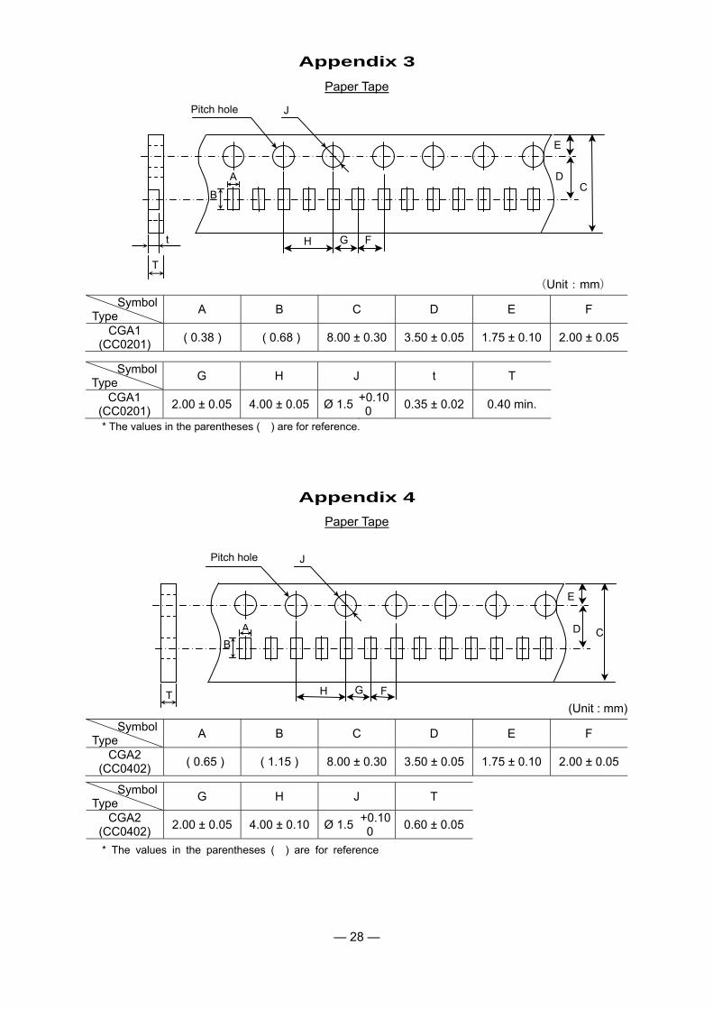
Appendix 3
Paper Tape
(Unit:mm)
Symbol Type
A B C D E F
CGA1 (CC0201)
( 0.38 ) ( 0.68 ) 8.00 ± 0.30 3.50 ± 0.05 1.75 ± 0.10 2.00 ± 0.05
Symbol
Type G H J t T
CGA1 (CC0201)
2.00 ± 0.05 4.00 ± 0.05 Ø 1.5+0.100
0.35 ± 0.02 0.40 min.
* The values in the parentheses ( ) are for reference.
Appendix 4
Paper Tape
(Unit : mm)
Symbol Type
A B C D E F
CGA2 (CC0402)
( 0.65 ) ( 1.15 ) 8.00 ± 0.30 3.50 ± 0.05 1.75 ± 0.10 2.00 ± 0.05
Symbol Type
G H J T
CGA2 (CC0402)
2.00 ± 0.05 4.00 ± 0.10 Ø 1.5+0.100
0.60 ± 0.05
* The values in the parentheses ( ) are for reference
T
A
J Pitch hole
H G F
B
E
D C
t
T
A
JPitch hole
H G F
B
E
D C

— 29 —
Appendix 5
Paper Tape
(Unit : mm)
Symbol Type
A B C D E F
CGA3 (CC0603)
( 1.10 ) ( 1.90 )
8.00 ± 0.30 3.50 ± 0.05 1.75 ± 0.10 4.00 ± 0.10CGA4
(CC0805) ( 1.50 ) ( 2.30 )
CGA5 (CC1206)
( 1.90 ) ( 3.50 )
Symbol Type
G H J T
CGA3 (CC0603)
2.00 ± 0.05 4.00 ± 0.10 Ø 1.5+0.100
1.20 max. CGA4
(CC0805) CGA5
(CC1206)
* The values in the parentheses ( ) are for reference.
T H G F
A
C
E
D
Pitch hole J
B
— 30 —
Appendix 6
Plastic Tape
(Unit : mm)
Symbol Type
A B C D E F
CGA3 (CC0603)
( 1.10 ) ( 1.90 )
8.00 ± 0.30
[12.0 ± 0.30]
3.50 ± 0.05
[5.50 ± 0.05]1.75 ± 0.10 4.00 ± 0.10
CGA4 (CC0805)
( 1.50 ) ( 2.30 )
CGA5 (CC1206)
( 1.90 ) ( 3.50 )
CGA6 (CC1210)
( 2.90 ) ( 3.60 )
Symbol Type
G H J K t Q
CGA3 (CC0603)
2.00 ± 0.05 4.00 ± 0.10 Ø 1.5+0.100
1.50 max.
0.30 max. Ø 0.50 min.
CGA4 (CC0805)
2.50 max. CGA5
(CC1206) CGA6
(CC1210) 3.20 max. 0.60 max.
* The values in the parentheses ( ) are for reference.
* As for 2.5mm thickness products, apply values in the brackets [ ].
t
K H G F
A
C
E
D
Pitch hole J
B
Q

— 31 —
Appendix 7
Plastic Tape
(Unit : mm)
Symbol Type
A B C D E F
CGA8 (CC1812)
( 3.60 ) ( 4.90 ) 12.0 ± 0.30 5.50 ± 0.05 1.75 ± 0.10 8.00 ± 0.10
CGA9 (CC2220)
( 5.40 ) ( 6.10 )
Symbol Type
G H J K t Q
CGA8 (CC1812)
2.00 ± 0.05 4.00 ± 0.10 Ø 1.5+0.100
6.50 max. 0.60 max. Ø 1.50 min.CGA9
(CC2220)
* The values in the parentheses ( ) are for reference.
t
K H G F
A
C
E
D
Pitch hole J
B
Q

— 32 —
Appendix 8 CGA1, CGA2, CGA3, CGA4, CGA5, CGA6 ( As for CGA6 type, any thickness of the item except 2.5mm )
(Material : Polystyrene)
(Unit : mm)
Symbol A B C D E W1
Dimension Ø178 ± 2.0 Ø60 ± 2.0 Ø13 ± 0.5 Ø21 ± 0.8 2.0 ± 0.5 9.0 ± 0.3
Symbol W2 r
Dimension 13.0 ± 1.4 1.0
Appendix 9 CGA6 ( Applied to 2.5mm thickness products ), CGA8, CGA9
(Material : Polystyrene)
(Unit : mm)
Symbol A B C D E W1
Dimension Ø178 ± 2.0 Ø60 ± 2.0 Ø13 ± 0.5 Ø21 ± 0.8 2.0 ± 0.5 13.0 ± 0.3
Symbol W2 r
Dimension 17.0 ± 1.4 1.0
B
W1 A
EC
Dr
W2
B
W1 A
EC
Dr
W2

— 33 —
Appendix 10 CGA1, CGA2, CGA3, CGA4, CGA5, CGA6 ( As for CGA6 type, any thickness of the item except 2.5mm )
(Material : Polystyrene)
(Unit : mm)
Symbol A B C D E W
Dimension Ø382 max. (Nominal
Ø330) Ø50 min. Ø13 ± 0.5 Ø21 ± 0.8 2.0 ± 0.5 10.0 ± 1.5
Symbol t r
Dimension 2.0 ± 0.5 1.0
Appendix 11 CGA6 (Applied to 2.5mm thickness products), CGA8, CGA9 (Material : Polystyrene)
(Unit : mm)
Symbol A B C D E W
Dimension Ø382 max. (Nominal
Ø330) Ø50 min. Ø13 ± 0.5 Ø21 ± 0.8 2.0 ± 0.5 14.0 ± 1.5
Symbol t r
Dimension 2.0 ± 0.5 1.0
B
WA
EC
Dr
t
B
WA
EC
Dr
t