1 an efficient transient electro-thermal simulation...
TRANSCRIPT
1
An Efficient Transient Electro-Thermal SimulationFramework for Power Integrated Circuits
Qinggao Mei†, Wim Schoenmaker‡, Shih-Hung Weng+, Hao Zhuang+, Chung-Kuan Cheng+ and Quan Chen†∗
Abstract—This paper presents a new transient electro-thermal(ET) simulation method for fast 3D chip-level analysis of powerelectronics with field solver accuracy. The metallization stackand substrate are meshed and solved with 3D field solver usingnonlinear temperature-dependent electrical and thermal param-eters, and the active transistors are modeled with table models toavoid time-consuming TCAD simulation. Two contributions aremade to enhance the physical relevance and the computationalperformance: 1) The capacitive effects, including interconnectparasitic capacitance and gate capacitance of power devices withnonlinear dependence on bias and temperature, are explicitlyaccounted for; 2) A specialized nonlinear exponential integrator(EI) method is developed to address the considerably differenttime scales between electrical and thermal sectors. The EI-basedtransient solver allows the electrical system to step with muchlarger time steps than in conventional methods, thus the time stepgap between the electrical and the thermal simulation is largelyreduced.
I. INTRODUCTION
Bipolar-CMOS-DMOS (BCD) integration is a key tech-nology for power integrated circuits (ICs), offering manyadvantages by integrating three distinct types of devices on asingle die. New challenges, however, have also been triggeredto the thermal managements in the BCD technology due tothe closer proximity of high-power DMOS transistors to othertemperature-sensitive components and the more complicatedgeometry and material configurations. Accurate prediction intemperature profile is needed to guide heat removal designand avoid potential reliability issues such as electromigrationand negative bias temperature instability (NBTI). To this end,the strong coupling between electrical and thermal dynamics,e.g., the nonlinear temperature dependencies of electrical pa-rameters and device characteristics [14], must be appropriatelyaccounted for. Therefore, an accurate transient electro-thermal(ET) co-simulation is highly desired to detect and avoidthermal failures in the early stage of BCD designs.
∗Corresponding author†The authors are with the Department of Electrical and Electronic Engi-
neering, The University of Hong Kong, Pokfulam Road, Hong Kong. E-mails:{qgmei,quanchen}@eee.hku.hk‡The author is with Magwel NV, Leuven, Belgium. E-mail:
[email protected]‡The authors are with the Department of Computer Science and Engi-
neering, The University of California, San Diego, La Jolla, USA. E-mails:{s2weng, ckcheng}@ucsd.edu and [email protected]
Copyright (c) 2015 IEEE. Personal use of this material is permitted.However, permission to use this material for any other purposes must beobtained from the IEEE by sending an email to [email protected]
In BCD technology, there is an increasing quest to modelmetal layers with high spatial resolution to predict accuratevoltage drop, since the resistance of the metal layer is increaseddue to the ever-decreasing wire width. To this end, [15]develops a new transient ET simulation approach in whichfield-based solution is also applied to the on-chip metallization,and coupled tightly with a whole-domain thermal field solver.The electrical and thermal behaviors of DMOS transistors aremodeled by nonlinear table models to avoid detailed time-consuming TCAD simulation. Being one step closer to the“ideal” full-physics simulation, the ET solver presented in [15]can determine the voltage drop in the metal structures and thedevice temperatures with high accuracy and without limitingthe applicability to special cases.
However, one simplification made in [15] and other workssuch as [8] is that the device responses are assumed instan-taneous. It is valid under small gate capacitance of devicesand low driving frequency, and leads to convenient numericaltreatment as no temporal differential equation needs to besolved in the electrical sector. The whole transient simulationcan then be carried on solely in the thermal time scale.Nevertheless, the electrical time scale becomes relevant whenthe devices contain a large summed gate capacitance, e.g.,with many fingers, and operate at relatively high switchingfrequencies. The capacitive effects of DMOS then need to betaken into account for accurate prediction of the voltage drop.
The inclusion of capacitive effects induces a challenge:the combined ET system contains considerably different timescales from electrical dynamics (ns to µs) and thermal dynam-ics (µs to ms). In other words the system is stiff. Simulatingthe electrical system using the step size dictated by the fastesttransients may require thousands of steps in one thermal stepand result in unnecessarily long simulation time. A commonstrategy to cope with this multi-scale property is to let the elec-trical and thermal solvers run at their own paces and exchangeinformation at the end of the larger (thermal) step [7], seeFig. 2. However, the smallest time constants in the electricalsimulation are typically induced by small parasitics in on-chipmetallization, which may require unnecessarily small step sizewhen conventional linear multi-step methods (LMMs) of loworders are employed.
In this paper, we aim to develop a numerically scalable ETcoupled simulator without assuming instantaneous electricalresponse. By relaxing the instantaneity assumption, the ca-pacitive effect (and inductive effect if needed) can be readilyincorporated in the simulation for better accuracy in high-frequency modeling. Yet the cost to pay is the necessity tointegrate a multi-scale system. We propose to mitigate this
2
difficulty using a specially designed time integration methodbased on the nonlinear exponential integrator (EI). The ideais to let the step size of the electrical system determined bythe slow-varying variables, which are typically related to theswitching of the power devices, instead of by the fast variablesrelating to the parasitics of metallic interconnects. Furtheracceleration techniques, such as adaptive time stepping, aredeveloped to expedite the EI-based transient solver.
II. DYNAMIC ELECTRO-THERMAL SIMULATIONSTRATEGY
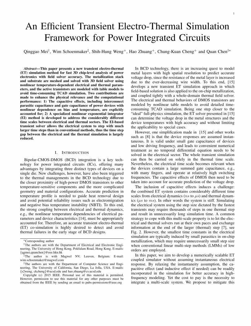
Fig. 1. Multi-domain ET modeling (the substrate are included in the thermalsolver but not in the electrical solver)
The transient ET co-simulator developed in this work isbased on the multi-domain modeling strategy illustrated inFig. 1 [9], [15]. If capacitive and inductive effects are ne-glected, the electrical system is characterized by the currentcontinuity equation
∇ · (Jc + Jd) = 0, (1)
where Jc is the conduction currents of the on-chip metallicstructures consisting of interconnects, vias and contacts, andJd is the drain-source currents of power devices
Jc = −σ (T )∇V, conductorsJd = f (Vgs, Vds, Tds) , power devices
(2)
In (2), Jc in the on-chip metallization is obtained by solvingthe electrical potential V (primary electrical variable) with afield solver using temperature-dependent conductivity σ (T ).Jd, on the other hand, is looked up from a temperature-aware table model to avoid expensive TCAD simulation. Vgs,Vds, and Tds denote the gate-source voltage, the drain-sourcevoltage and the device temperature averaged at the source anddrain terminals, respectively. To link the table models to thefield solvers, the channel layers of the MOS devices, whichare geometrically negligible compared to the size of die, areeffectively “removed” from the 3D mesh of the substrate.Relevant terminal voltages, e.g., Vgs and Vds, are measuredat proper metal ends and passed to the table model, which
in turn generates currents as external current sources at thecorresponding terminals in the field solving process.
To model the thermal dynamics, the heat conduction equa-tion is solved on the entire domain with a thermal field solver
CT∂T
∂t−∇ · (κ(T )∇T )−Q = 0, (3)
where T is the temperature (primary thermal variable), κ(T )the temperature-dependent thermal conductivity, CT the vol-umetric heat capacity and Q the heat sources or sinks. TheQ term in (3) has several contributors: 1) the Joule self-heating of the metal structures; 2) the self-heating of the activedevices and 3) heat injected or extracted at the boundary of thesimulation domain. Similar to [15], the first two contributionsare calculated by
Q =
{E · J = σ(T )|∇V |2, conductorsJds · Vds, power devices (4)
from the information provided by the electrical solver. Thethird one is modeled by thermal contacts placed on the domainboundary enforcing fixed temperatures or fixed heat flux.
The temperature-dependent models of the electrical and thethermal conductivities are given by the exponential models
σ(T ) = σ0
(T
T0
)ασ, (5)
κ(T ) = κ0
(T
T0
)ακ, (6)
where the exponents ασ and ακ are material-dependentparameters. Other material parameters are assumed to betemperature-independent.
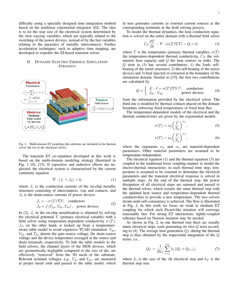
The electrical equation (1) and the thermal equation (3) arecoupled in the traditional loose coupling manner to model theelectro-thermal interactions: in each thermal time step, tem-perature is assumed to be constant to determine the electricalparameters and the transient electrical response is solved inmultiple steps. At the end of the thermal step, the powerdissipation of all electrical steps are summed and passed tothe thermal solver, which restarts the same thermal step withthe updated heat source and temperature-dependent thermalconductivities to provide a new temperature. The two solversiterate until self-consistency is achieved. The flow is illustratedin Fig. 2. In this work we focus on weak to medium ETcoupling for which such Picard-like iteration will convergereasonably fast. For strong ET interactions, tightly-coupledschemes based on Newton iteration may be needed.
As shown in Fig. 2, in one thermal step there are usuallymany electrical steps, each generating its own Q term accord-ing to (4). The average heat generation QT during the thermalstep is then obtained by the trapezoidal integration of the Qterms, i.e.,
QT =1
2hT
nE∑i=1
hi (Qi +Qi+1), (7)
where hi is the size of the ith electrical step and hT is thethermal step size.
3
Fig. 2. Electro-Thermal simulator coupling for one (thermal) step.
III. MODELING OF CAPACITANCE
One assumption we made in [15] is that all capacitive effectsare neglected, resulting in equation (1) that is an algebraicLaplacian equation with its solution solely determined bythe instantaneous boundary condition. In other words, theelectrical step size can be arbitrary and even equal to thethermal step size (corresponding to k = 1 in Fig. 2). Thisnumerically convenient assumption is valid for low-frequencyapplication, but will affect the modeling accuracy for scenarioswith nontrivial capacitive effects, such as devices with alarge number of transistor fingers and in microwave applica-tions [16]. Therefore, one contribution of this work is to modelthese capacitive effects explicitly so that the electrical systemno longer responds instantaneously to the applied voltages inthe field solving.
To account for the parasitic capacitances of the back-endstructures, the displacement current is added to the currentcontinuity equation (1), leading to
−∇(ε∇∂V
∂t
)+∇ · J = 0 (8)
For modeling the gate capacitance of DMOS, each polysil-icon finger is divided up into equal sections, and for eachsection one gate-source capacitance Cgs and one gate-draincapacitance Cgd are attached, which are modeled as externalcapacitors in the field solving process of the back-end struc-tures. To account for the charging and discharging currentsof the capacitors, extra terms are added to (1) when solvedat relevant nodes. For instance, the equation at a gate nodebecomes
−∇(ε∇∂V
∂t
)+∇·J+Cgs
∂(Vg − Vs)∂t
+Cgd∂(Vg − Vd)
∂t= 0,
(9)where capacitive current paths are introduced between the gateand the source (drain) terminals. Note that the gate capacitanceis generally dominant over the parasitic capacitance of metalwires.
The values of the devices capacitors are determined by thecompact model of DMOS [6], which is a nonlinear functionof the applied biases and the temperature as shown in (10).CGS1−GS6 and CGD1−GD4 are the model coefficients for Cgsand Cgd, respectively. These coefficients can be fitted for target
devices using the procedures in [6]. The introduction of thenonlinear capacitance term requires special treatments in theEI method, which will be detailed in the later sections.
IV. FAST ELECTRICAL SOLVER BASED ON EIThere are three typical time scales involved in the filed-
solver based ET simulation: the time scale attributed to in-terconnect parasitics, the time scale related to power deviceswitching and that on which temperatures vary. The intercon-nect time scale is the shortest one, ranging from ps to ns,the thermal time scale is the largest one on the order of µsto ms, and the power device switching one (ns to µs) issomewhere in-between. Solving the electrical system by LMMusually requires step sizes small enough to resolve the fastinterconnect transients that are several orders faster than thethermal dynamics and thus a great number of electrical stepsare to be nested in one thermal step (a large k in Fig. 2).
Nevertheless, an accurate capture of the fine-scale details ofelectrical waveform may not be truly necessary for temperatureprediction. The extremely short duration of parasitic transientslimits the amount of heat generation. Consequently, the powerdissipation originates mainly from power devices operatingwith high currents and voltages, and to a lesser degree fromon chip metallization. The pace of heat generation in powerdevices depends on the switching frequency and is usuallyslower than in interconnects due to the relatively large devicecapacitance. In other words, the temperature variation maystill be predicted to a reasonable extent, provided that therelatively slow-varying heat generation from power devices isproperly captured even on a coarser time scale. The accuratecharacterization of on-chip metallization is more for providingcorrect voltage drops to determine the operation status ofpower devices, than in computing the Joule heating of themetal structure itself [15].
Relaxing time step size is a challenge to traditional low-order LMM methods in the electrical solution. The minimalstep size is dictated by the smallest time constant incurredgenerally by the small parasitics in metal wires. Simplyincreasing step size to bypass the fast transients is risky andmay lead to large linear truncation error (LTE) and eventuallyerroneous simulation. Hence, it is desired to develop high-order transient simulation techniques that can skip the fast yetless important transient variations in metallization in a safemanner, and allow the electrical system to be simulated at thesame pace as the power devices operate. To this end, we extendthe EI method to the electrical solver in the proposed transientET simulation framework. On the other hand, the time scalesin the thermal sector do not differ significantly because of thesimilar thermal capacitance of different materials, therefore westill apply LMM as the thermal solver.
The basic idea of EI is that the solution of an ODE x = Axat time point tn+1 can be linked analytically to its solution attn by
xn+1 = eAhxn (11)
where h is the time step size. This expression is exact in thesense that one can step with arbitrary h if the matrix expo-nential term is evaluated accurately enough. The difficulty of

4
Cgs = (CGS1 + CGS2 [1 + tanh (CGS6 (Vgs + CGS3))] + CGS4 [1− tanh (CGS5Vgs)]) (1 + CGS6 (T − T0))
Cgd =
[CGD1 +
CGD2
1 + CGD3(Vgd − CGD4)2
](1 + CGD0 (T − T0))
(10)
using (11) directly lies in that computing matrix exponentials(or the products with vectors) has long been more expensivethan solving linear systems. As a consequence, traditionalLMMs seek to approximate (11) with a function involvingmatrix inverse only [4], which induces LTE inevitably. Thesituation was changed by the emergence of new numericalmethods such as the Krylov subspace methods, which makethe computation of matrix exponential-vector product feasiblefor large sparse matrices [11]
The EI is attractive because it integrates the linear ODEsystem exactly and thus may permit larger time steps tonarrow down the gap between the electrical and thermal stepsizes. Since the troublemaker, the small interconnect parasiticcapacitance, is linear by nature, its limitation on the stepsize can be removed in the first place by using EI [4]. Theerror of EI for linear systems only arises from the numericalcomputation of the matrix exponential (more precisely theproduct of matrix exponential with a vector), and the orderof accuracy can be made fairly high to safely bypass thefast transients induced by the back-end linear structures [17].The step size is instead limited by the approximation of thenonlinear terms, which relate to the power devices operatingat a slower pace.
A nonlinear EI-based transient solver, a.k.a. the matrixexponential method, has been developed in [17] for circuitsimulation. The nonlinear subsystem is decoupled from thelinear one by an integration factor technique, leading toconvenient separation between the matrix exponential termand the nonlinear function [12]. That scheme, however, is notreadily applicable to the ET simulation of interest in this workfor several reasons. The circuit simulation concerns mainlydigital and analog circuits with signal MOSFETs operatingcomparably fast with interconnects, and the short-durationtransients are of practical interest and should be observed withsmall time steps. In such context the error of the decoupledapproximation of the nonlinear term remains reasonable. Yetthe situation is different in the ET simulation. Since the powerdevices are much slower than the interconnect response and wewould like to use large steps to bypass fine-scale details that arenot needed for thermal calculation, large error will be inducedif the decoupled approximation is used, as will be analyzedin the next subsection. To truly push the step size to the limitof the electrical sector in ET analysis, different treatments tothe nonlinear terms are needed and will be detailed in thefollowing subsections.
A. Formulation of Nonlinear EI
The electrical equation (9), after the finite volume dis-cretization [3], can be cast into a general differential-algebraic
equation (DAE)
C(x)dx
dt= −Gx− I(x)− b, (12)
where C(x) collects both the interconnect and device capac-itance terms and is nonlinear due to the device capacitancemodel, G collects the interconnect conductance (a constantmatrix in one thermal step as the metal conductivities dependon temperature only) and x is the nodal potentials to be solved.The nonlinear function I(x) stores the nonlinear currents Idsof power devices evaluated from the table models. The vectorb represents the voltage and/or current sources which areassumed piece-wise linear in each step. Generally, C(x) issingular because the Gauss law does not contain time differ-entiation term. The singularity however can be convenientlyremoved by an explicit differentiation of the Gauss law [3].
The nonlinearity present in C(x) prevents the direct appli-cation of EI, which is essentially a linear time integrator. Toaddress this, we decompose C(x) as
C(x) = C + ∆C (x) (13)
where the constant matrix C = C (x0) collects all the(linear) interconnect parasitic capacitance as well as the devicecapacitance evaluated at the DC bias x0. The nonlinear ∆C (x)describes only the dependence of the device capacitance on thestate variable x. Such decomposition allows us to rewrite (12)into
Cx = −Gx− [I(x) + ∆C(x)x]− b= −Gx− F (x, x)− b (14)
Defining A = −C−1G, we can transform the DAE (12) toan ODE
dx
dt= Ax− C−1F (x, x)− C−1b, (15)
The exact solution of (15) is expressed by the followingformula with matrix exponential
xn+1 = eAhxn+∫ h
0
eA(h−τ) [−C−1F (tn + τ)− C−1b(tn + τ)]dτ.
(16)
One key step of nonlinear EI is to approximate the integralinvolving the nonlinear function F (τ). Implicit approximationof F (τ) together with the Newton’s method is difficult, as itinvolves the multiplication of a matrix exponential eA with theJacobian matrix of F (τ) that varies in each Newton iteration.In [4], a more efficient nonlinear EI was developed whichdecouples the EI and the nonlinear function using integrationfactor. However, the decoupled formulation suites better forthe case when F (τ) itself is stiff and of a comparable scale
5
with the interconnect parasitics [12], whereas not suitable forthe ET problems where the F function is generally not stiffbecause of the comparably large terminal capacitance amongpower devices.
In this work we choose the second-order Runge-Kutta (RK)approximation of F [5], to solve (16). Solution of the (n+1)thstep is obtained by
an = eAhxn + hψ1 (Ah)w1
xn+1 = an + h2ψ2 (Ah)w2, (17)
where the ψ-functions of different orders are defined as
ψ1 (x) =ex − 1
x, ψ2 (x) =
ex − x− 1
x2,
and w1 and w2 are
w1 = −C−1 (Fn + bn) , w2 = −C−1F (an)− Fnh
. (18)
Here an is an intermediate solution of potential obtained froma forward Euler step from the nth step. In our problem we usemostly voltage excitation, so for convenience we differentiatethe piece-wise linear inputs. Therefore bn becomes constantwithin a step and a diagonal 1 is introduced to C for eachinput node. For F (x, x) we evaluate it as
F (x, x)n+1 = F
(xn+1,
xn+1 − xnhn+1
), (19)
and consequently
Fn = F (xn) = F (xn, 0) , F (an) = F
(an,
an − xnhn+1
)Note that in (19) we introduce the first order finite differenceapproximation for the derivative of x. It is justified as thevoltage dependence of device capacitance is mild and, moreimportantly, the ∆C(x)x term has only nonzeros at the termi-nals of power devices, where the potentials vary smoothly dueto the relatively large capacitance attached to these terminals.The residual due to the RK approximation of the nonlinearterm is
resNL ∼ −h3
12‖F‖. (20)
It is noteworthy to compare (20) against the residual estimateof the decoupled scheme [17]
resNL ∼ −h3
12‖(A2F +AF + F
)‖. (21)
For stiff problems, ‖A‖ tends to be large, the first term in theresidual of the decoupled scheme will become dominant andprevents the use of large step size. In fact the EI in (17) is basedon a polynomial approximation of F (τ), whereas the decou-pled scheme is obtained from approximating e−AτF (τ) [12].Since −A has positive eigenvalues, e−AτF (τ) requires a veryhigh order of polynomial to maintain approximation accuracywhen the norm of A is large, even when F (τ) itself is a smoothfunction. Consequently, the nonlinear EI formulation (17) ismore suitable in this scenario.
The summation of the ψ-functions in (17) can be calcu-lated by evaluating the exponential of a slightly augmentedmatrix [2].[
an∗
]= exp
(Aah
)xn = exp
([A Wa
0 J2
]h
)[xne2
][xn+1
∗
]= exp
(Ah)xn = exp
([A W0 J2
]h
)[xne2
],(22)
whereWa = [ 0 w1 ] , W = [ w2 w1 ] , (23)
and
J2 =
[0 10 0
], e2 =
[01
].
B. Computation of eAhv via rational Krylov subspace methodIn (22), the core computation in EI is the product of
matrix exponential times a vector eAv. Among many numericalapproaches to evaluate this term [10], Krylov subspace-basedapproximation is one of the few considered as scalable tomillion-scale problems [3], [17]. Nevertheless, our target stepsize is rather aggressive compared to those have been reportedin [3], [18], and EI based on the ordinary Krylov subspaceis known to be not competitive in this scenario as it doesnot approximate large-magnitude eigenvalues (correspondingto the slow transients) accurately enough [4]. Therefore, inthis work we choose EI based on the shift-and-invert (SAI)Krylov subspace which provides a better approximation to theslow manifold of the waveform to allow larger step sizes [19],[20].
The main step of the SAI Krylov subspace approximationis an m-step Arnoldi process applied to (I − γA)−1
(I − γA)−1Vm = VmHm +H(m+ 1,m)vm+1eTm, . (24)
Vm is an orthonormal basis of the m-dimensional Krylovsubspace Km
((I − γA)−1, v
)with γ being a shift parameter,
and vm+1 is an additional basis vector to make [Vm, vm+1]an orthonormal basis of Km+1
((I − γA)−1, v
). H is an
(m + 1) × m upper Hessenberg coefficient matrix resultingfrom the modified Gram-Schmidt process, in which Hm is theleading m×m submatrix and H(m+ 1,m) is the element atthe lower-right corner. ei, i = 1, 2, ..,m is the ith column ofan m ×m identity matrix and the superscript T denotes thetranspose. Then the EI-vector product is approximated as itsorthogonal projection onto the SAI Krylov subspace
eAhv ≈ VmV Tm eAhv = βVmeHmh/γe1, (25)
withHm =
(I −H−1
m
), β = ‖v‖2
We measure the approximation quality of (25) using theposteriori residual estimate developed in [21] without requiringC−1
resKry =β
γH(m+ 1,m)‖(C + γG)vm+1e
TmH
−1m eHmh/γe1‖.
(26)
6
in which C+γG = C(I−γA). Note that the major advantageof the SAI Krylov subspace over the ordinary one is the smallersubspace dimension required to integrate stiff systems withlarge step sizes [20]. In our experiments m is generally below40 and thus storing the basis vectors is not memory demanding.This also facilitates the design of adaptive stepping as will bediscussed later.
Since Wa and W are different and they change every step,in principle one needs to factorize two matrices, I − γAa andI − γA, in each time step to generate two Krylov subspacesfor approximating (22). However, the leading parts of thesematrices are the same A, and one can take advantage of thisfact to reduce the number of matrix factorizations to one [19].For instance, rewrite(I − γAa
)−1
v =
[(C + γG) −γWa
0 I2 − γJ2
]−1 [C 00 I2
]v.
(27)Let LU = (C + γG) be the LU factorization of (C + γG),then the LU factors of
(I − γAa
)can be obtained by aug-
menting L and U as
L =
[L 00 I2
], U =
[U −L−1 (γWa)0 I2 − γJ2
], (28)
where the additional cost is only the forward substitutionsL−1 (γWa). The LU updates for A follow similarly. Con-sequently, only one LU factorization is needed at the verybeginning of each thermal step, within which C and G areconstant, and the LU factors can be stored and reused to solveall the linear systems involved economically.
C. Adaptive Nonlinear EI
Although constant step size is convenient for implementa-tion, adaptive time stepping generally offers better accuracyand performance during transient simulation. Adaptivity is par-ticularly desirable in ET co-simulation since the conductivities,and thus the electrical time constants, may vary substantiallywith the temperature, rendering an a priori step size selectionmore difficult and less efficient. Like the ordinary version,the SAI Krylov subspace also processes the scaling invariantproperty that allows convenient re-computation of the solutionwithout generating a new subspace. When the step size ischanged from h1 to h2, the new solution can be updated via
eAh2v ≈ βVmeHmh2/γe1, (29)
where Vm and Hm in (24) are re-used, and only a smallmatrix exponential needs to be re-evaluated. This is a markedadvantage. LMM methods require a new matrix factorizationwhenever the step size is changed, and as such tend to leverageadaptivity in a “passive” fashion, i.e., current step size can onlybe reduced to meet accuracy requirement, and increase of stepsize is possible only in the next step [3]. In contrast, EI-basedmethods are more “proactive” in utilizing adaptive stepping.Because of the ease in re-computing solution for new stepsizes, the size of current step can be adjusted multiple times
to best utilize error margin and minimize the number of totaltime steps.
However, the development of adaptive scheme is morecomplicated with the nonlinear EI formulation (22) and (23).Due to the dependence of W (more exactly w2) on thenonlinear function F (an), xn+1 cannot be re-evaluated bysimple scaling as A becomes different when an is updatedwith a different step size. Consequently, a new Arnoldi processneeds to be performed with respect to the modified A, incurringpossibly nontrivial overhead. In the following, we develop amore efficient adaptive scheme than directly computing xn+1
as in (22).For clarity, we rewrite (22) for step size h1 as
a(1)n = exp(Aah1
)xn, x
(1)n+1 = exp
(A(1)h1
)xn. (30)
Using the Krylov subspace approximation (25), we compute(30) by
a(1)n ≈ βV (a)m eH
(a)m h1/γe1 (31a)
x(1)n+1 ≈ βV (1)
m eH(1)m h1/γe1. (31b)
When the step size is changed from h1 to h2, the new an canstill be updated by re-scaling (31a) since Aa and xn are fixed
a(2)n ≈ βV (a)m eH
(a)m h2/γe1. (32)
To compute x(2)n+1, in principle one needs a new Arnoldi
process, operating on A2h2 and xn, to generate V(2)m , H
(2)m ,
then approximates,
x(2)n+1 ≈ βV (2)
m eH(2)m h2/γe1. (33)
Yet a closer observation reveals that the second vector in W (1)
and W (2), i.e., w1, is independent of the step size, and only thefirst vector w2 is different. Therefore, x(2)n+1 can be computedalternatively by the following identity
x(2)n+1 = exp
(A(1)h2
)xn + exp
(A(3)h2
)z2, (34)
where
A(3) =
[A W (2) −W (1)
0 J2
], z2 =
[0e2
].
The first term in (34) can be approximated by re-scaling(31b)
exp(A(1)h2
)xn ≈ βV (1)
m eH(1)m h2/γe1.
The Krylov approximation of the second term in (34) requiresan Arnoldi process with A(3)h2 and z2. The advantage of thisupdating scheme lies in that z2 is generally of small normand thus the Arnoldi process needs fewer iterations to achieveconvergence than using A2h2 and xn directly.
To simplify the design of adaptive stepping, we adjustthe step size only according to the nonlinear approximationresidual (20). Given a prescribed absolute tolerance tola and
7
a relative tolerance tolr, the maximum step size is determinedby
hmax = min
((tolNL
resNL
)1/3), (35)
with
tolNL = tola + tolr max (|xn+1| , |xn|) .
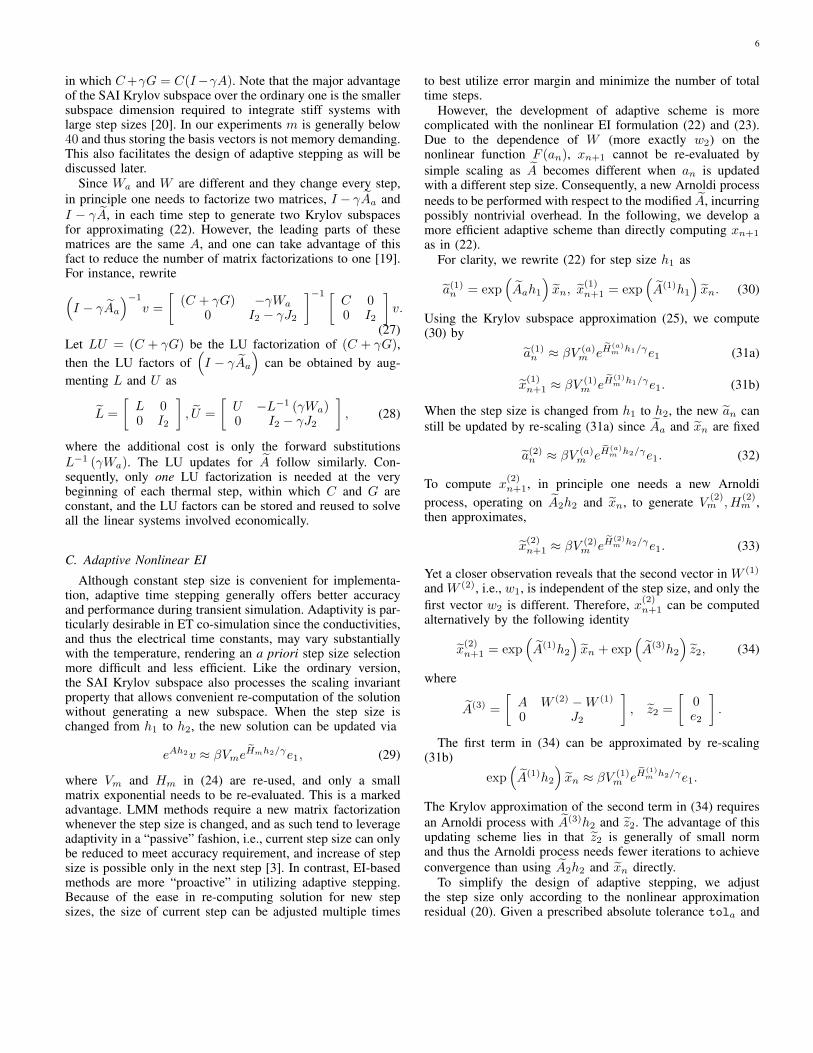
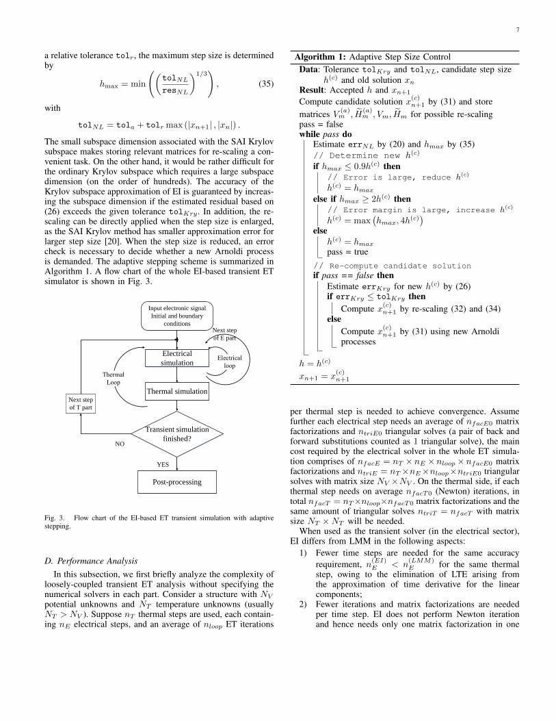
The small subspace dimension associated with the SAI Krylovsubspace makes storing relevant matrices for re-scaling a con-venient task. On the other hand, it would be rather difficult forthe ordinary Krylov subspace which requires a large subspacedimension (on the order of hundreds). The accuracy of theKrylov subspace approximation of EI is guaranteed by increas-ing the subspace dimension if the estimated residual based on(26) exceeds the given tolerance tolKry. In addition, the re-scaling can be directly applied when the step size is enlarged,as the SAI Krylov method has smaller approximation error forlarger step size [20]. When the step size is reduced, an errorcheck is necessary to decide whether a new Arnoldi processis demanded. The adaptive stepping scheme is summarized inAlgorithm 1. A flow chart of the whole EI-based transient ETsimulator is shown in Fig. 3.
Input electronic signal
Initial and boundary
conditions
Electrical
simulation
Thermal simulation
Post-processing
Transient simulation
finished?
Next step
of E part
Next step
of T part
NO
YES
Fig. 3. Flow chart of the EI-based ET transient simulation with adaptivestepping.
D. Performance AnalysisIn this subsection, we first briefly analyze the complexity of
loosely-coupled transient ET analysis without specifying thenumerical solvers in each part. Consider a structure with NVpotential unknowns and NT temperature unknowns (usuallyNT > NV ). Suppose nT thermal steps are used, each contain-ing nE electrical steps, and an average of nloop ET iterations
Algorithm 1: Adaptive Step Size ControlData: Tolerance tolKry and tolNL, candidate step size
h(c) and old solution xnResult: Accepted h and xn+1
Compute candidate solution x(c)n+1 by (31) and storematrices V (a)
m , H(a)m , Vm, Hm for possible re-scaling
pass = falsewhile pass do
Estimate errNL by (20) and hmax by (35)// Determine new h(c)
if hmax ≤ 0.9h(c) then// Error is large, reduce h(c)
h(c) = hmaxelse if hmax ≥ 2h(c) then
// Error margin is large, increase h(c)
h(c) = max(hmax, 4h
(c))
elseh(c) = hmaxpass = true
// Re-compute candidate solutionif pass == false then
Estimate errKry for new h(c) by (26)if errKry ≤ tolKry then
Compute x(c)n+1 by re-scaling (32) and (34)else
Compute x(c)n+1 by (31) using new Arnoldiprocesses
h = h(c)
xn+1 = x(c)n+1
per thermal step is needed to achieve convergence. Assumefurther each electrical step needs an average of nfacE0 matrixfactorizations and ntriE0 triangular solves (a pair of back andforward substitutions counted as 1 triangular solve), the maincost required by the electrical solver in the whole ET simula-tion comprises of nfacE = nT × nE × nloop × nfacE0 matrixfactorizations and ntriE = nT ×nE×nloop×ntriE0 triangularsolves with matrix size NV ×NV . On the thermal side, if eachthermal step needs on average nfacT0 (Newton) iterations, intotal nfacT = nT×nloop×nfacT0 matrix factorizations and thesame amount of triangular solves ntriT = nfacT with matrixsize NT ×NT will be needed.
When used as the transient solver (in the electrical sector),EI differs from LMM in the following aspects:
1) Fewer time steps are needed for the same accuracyrequirement, n(EI)E < n
(LMM)E for the same thermal
step, owing to the elimination of LTE arising fromthe approximation of time derivative for the linearcomponents;
2) Fewer iterations and matrix factorizations are neededper time step. EI does not perform Newton iterationand hence needs only one matrix factorization in one
8
step, whereas LMMs generally require factorizations ofmultiple Jacobians. This could be a shortcoming forEI when the step size is constrained by the nonlin-earity, which favors the Newton’s method for betterconvergence. However, when back-end metallizationsare included, the step size is mostly limited by the smalllinear parasitics, other than the nonlinearity induced bypower devices;
3) The saving in the number of matrix factorizations fromEI is more significant in adaptive time stepping. LMM-type methods need multiple factorizations of Jacobianmatrices in one step, and if the step is rejected, a new setof factorizations have to be performed as the Jacobiansare dependent on step size. In contrast, the adaptive EIrequires only one matrix factorization regardless of thetimes of step size adjustments, owing to the augmentedLU update scheme (28) and the scaling invariance ofKrylov subspace approximation.
V. NUMERICAL RESULTS
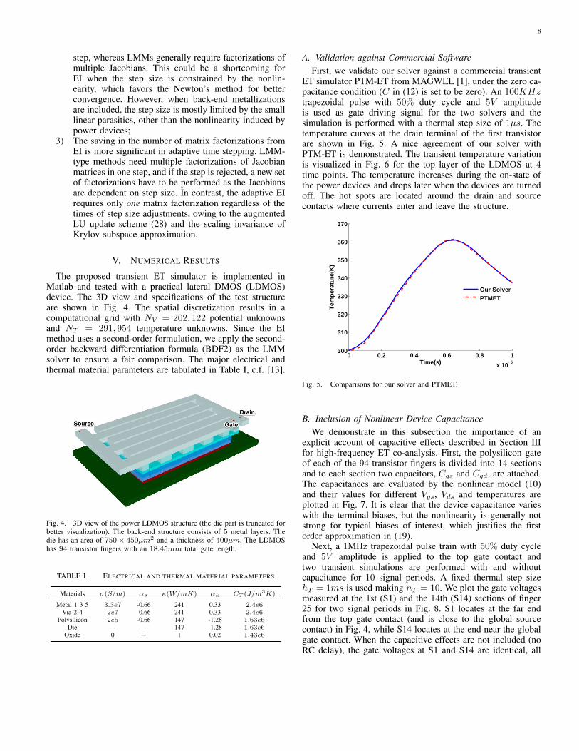
The proposed transient ET simulator is implemented inMatlab and tested with a practical lateral DMOS (LDMOS)device. The 3D view and specifications of the test structureare shown in Fig. 4. The spatial discretization results in acomputational grid with NV = 202, 122 potential unknownsand NT = 291, 954 temperature unknowns. Since the EImethod uses a second-order formulation, we apply the second-order backward differentiation formula (BDF2) as the LMMsolver to ensure a fair comparison. The major electrical andthermal material parameters are tabulated in Table I, c.f. [13].
Fig. 4. 3D view of the power LDMOS structure (the die part is truncated forbetter visualization). The back-end structure consists of 5 metal layers. Thedie has an area of 750× 450µm2 and a thickness of 400µm. The LDMOShas 94 transistor fingers with an 18.45mm total gate length.
TABLE I. ELECTRICAL AND THERMAL MATERIAL PARAMETERS
Materials σ(S/m) ασ κ(W/mK) ακ CT (J/m3K)
Metal 1 3 5 3.3e7 -0.66 241 0.33 2.4e6Via 2 4 2e7 -0.66 241 0.33 2.4e6
Polysilicon 2e5 -0.66 147 -1.28 1.63e6Die − − 147 -1.28 1.63e6
Oxide 0 − 1 0.02 1.43e6
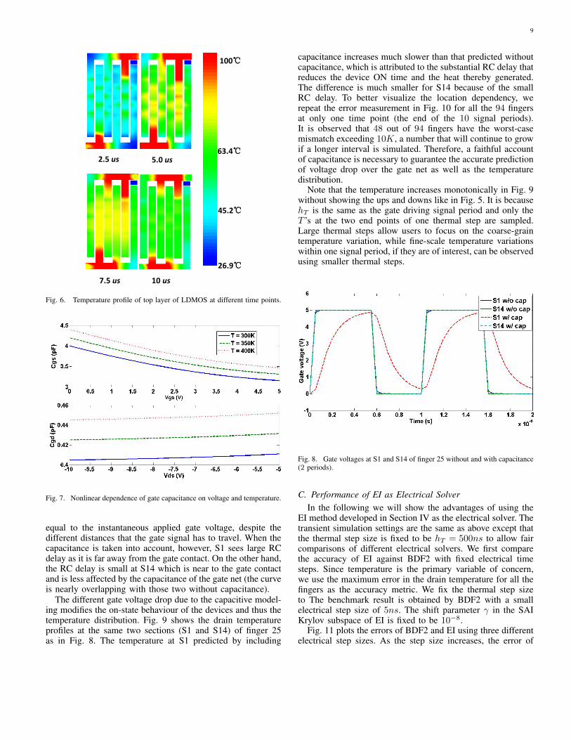
A. Validation against Commercial SoftwareFirst, we validate our solver against a commercial transient
ET simulator PTM-ET from MAGWEL [1], under the zero ca-pacitance condition (C in (12) is set to be zero). An 100KHztrapezoidal pulse with 50% duty cycle and 5V amplitudeis used as gate driving signal for the two solvers and thesimulation is performed with a thermal step size of 1µs. Thetemperature curves at the drain terminal of the first transistorare shown in Fig. 5. A nice agreement of our solver withPTM-ET is demonstrated. The transient temperature variationis visualized in Fig. 6 for the top layer of the LDMOS at 4time points. The temperature increases during the on-state ofthe power devices and drops later when the devices are turnedoff. The hot spots are located around the drain and sourcecontacts where currents enter and leave the structure.
0 0.2 0.4 0.6 0.8 1
x 10−5
300
310
320
330
340
350
360
370
Time(s)
Tem
pera
ture
(K)
Our SolverPTMET
Fig. 5. Comparisons for our solver and PTMET.
B. Inclusion of Nonlinear Device CapacitanceWe demonstrate in this subsection the importance of an
explicit account of capacitive effects described in Section IIIfor high-frequency ET co-analysis. First, the polysilicon gateof each of the 94 transistor fingers is divided into 14 sectionsand to each section two capacitors, Cgs and Cgd, are attached.The capacitances are evaluated by the nonlinear model (10)and their values for different Vgs, Vds and temperatures areplotted in Fig. 7. It is clear that the device capacitance varieswith the terminal biases, but the nonlinearity is generally notstrong for typical biases of interest, which justifies the firstorder approximation in (19).
Next, a 1MHz trapezoidal pulse train with 50% duty cycleand 5V amplitude is applied to the top gate contact andtwo transient simulations are performed with and withoutcapacitance for 10 signal periods. A fixed thermal step sizehT = 1ms is used making nT = 10. We plot the gate voltagesmeasured at the 1st (S1) and the 14th (S14) sections of finger25 for two signal periods in Fig. 8. S1 locates at the far endfrom the top gate contact (and is close to the global sourcecontact) in Fig. 4, while S14 locates at the end near the globalgate contact. When the capacitive effects are not included (noRC delay), the gate voltages at S1 and S14 are identical, all
9
100℃
26.9℃
45.2℃
63.4℃ 2.5 us 5.0 us
7.5 us 10 us
Fig. 6. Temperature profile of top layer of LDMOS at different time points.
Fig. 7. Nonlinear dependence of gate capacitance on voltage and temperature.
equal to the instantaneous applied gate voltage, despite thedifferent distances that the gate signal has to travel. When thecapacitance is taken into account, however, S1 sees large RCdelay as it is far away from the gate contact. On the other hand,the RC delay is small at S14 which is near to the gate contactand is less affected by the capacitance of the gate net (the curveis nearly overlapping with those two without capacitance).
The different gate voltage drop due to the capacitive model-ing modifies the on-state behaviour of the devices and thus thetemperature distribution. Fig. 9 shows the drain temperatureprofiles at the same two sections (S1 and S14) of finger 25as in Fig. 8. The temperature at S1 predicted by including
capacitance increases much slower than that predicted withoutcapacitance, which is attributed to the substantial RC delay thatreduces the device ON time and the heat thereby generated.The difference is much smaller for S14 because of the smallRC delay. To better visualize the location dependency, werepeat the error measurement in Fig. 10 for all the 94 fingersat only one time point (the end of the 10 signal periods).It is observed that 48 out of 94 fingers have the worst-casemismatch exceeding 10K, a number that will continue to growif a longer interval is simulated. Therefore, a faithful accountof capacitance is necessary to guarantee the accurate predictionof voltage drop over the gate net as well as the temperaturedistribution.
Note that the temperature increases monotonically in Fig. 9without showing the ups and downs like in Fig. 5. It is becausehT is the same as the gate driving signal period and only theT ’s at the two end points of one thermal step are sampled.Large thermal steps allow users to focus on the coarse-graintemperature variation, while fine-scale temperature variationswithin one signal period, if they are of interest, can be observedusing smaller thermal steps.
Fig. 8. Gate voltages at S1 and S14 of finger 25 without and with capacitance(2 periods).
C. Performance of EI as Electrical SolverIn the following we will show the advantages of using the
EI method developed in Section IV as the electrical solver. Thetransient simulation settings are the same as above except thatthe thermal step size is fixed to be hT = 500ns to allow faircomparisons of different electrical solvers. We first comparethe accuracy of EI against BDF2 with fixed electrical timesteps. Since temperature is the primary variable of concern,we use the maximum error in the drain temperature for all thefingers as the accuracy metric. We fix the thermal step sizeto The benchmark result is obtained by BDF2 with a smallelectrical step size of 5ns. The shift parameter γ in the SAIKrylov subspace of EI is fixed to be 10−8.
Fig. 11 plots the errors of BDF2 and EI using three differentelectrical step sizes. As the step size increases, the error of

10
Fig. 9. Drain temperatures at S1 and S14 of finger 25 without and withcapacitance (10 periods).
Fig. 10. Maximum temperature difference with and without capacitive effects(end of 20 periods, drain terminals of all the 94 fingers ).
BDF2 grows rapidly due to the less accurate voltage waveformprediction resulted from the linear LTE. On the other hand,EI maintains a comparable accuracy for 5X larger step size,thanks to the elimination of linear LTE in the first place. Thisway the gap between the electrical and the thermal step size(500ns) is substantially reduced.
Table II summarizes the performance data for the threefixed step sizes in Fig. 11. All the variables are of thesame definitions as in Section IV-D. The ET convergencetolerance is measured by ‖Tnew − Told‖/‖Told‖ < 10−4. Theconvergence criteria for the Newton iteration in BDF2 and theSAI Krylov approximation (tolKry) in EI are both set to be10−5. The thermal solver is the same (BDF2) for the two casesand thus the performance is similar. Several observations canbe made to Table II. First, the electrical solver takes up amajority of the total runtime due to the large number of timesteps, rendering improvement on its performance particularly
Fig. 11. Error in drain temperature of BDF2 and EI for fixed step sizes.
important for overall efficiency. Second, BDF2 consumes morematrix factorizations due to the Newton iterations in each step.The number of matrix factorizations can be reduced by usingfewer steps with larger sizes, but the error grows quickly asdemonstrated in Fig. 11. On the other hand, EI based onthe SAI Krylov subspace uses only one matrix factorizationregardless of the step sizes and the error increases only slowly.Third, for the triangular solves, BDF2 needs exactly one solvefollowing each matrix factorization, whereas EI requires muchmore when building the SAI Krylov subspace basis in (24),equivalent to solving a linear system with multiple right-hand-side vectors. It is well known that triangular solve is muchcheaper and more scalable than matrix factorization, and forthe tested matrix size one matrix factorization takes 3.42swhile a triangular solve needs only 0.1s. In terms of theruntime, if we compare BDF2 with 10ns and EI with 50nsthat provide comparable accuracy in temperature prediction,EI is faster than BDF2 by more than an order of magnitude.
We also investigate the impact of different thermal step sizeshT on the ET convergence property in Table IV. The same ETconvergence criterion as above and the fixed-step EI with hE =25ns are used. The number of ET loops are recorded for thefirst thermal step. Generally, large thermal steps require moreET iterations to achieve convergence when the temperaturevariation is more significant within the step inducing strongerET iterations.
TABLE IV. ET CONVERGENCE FOR DIFFERENT THERMAL STEP SIZES
hT (ns) nloop
500 31000 42500 55000 7
We then compare BDF2 and EI using adaptive step sizes. InBDF2 the hmax is determined by (35) using the LTE estimate− 2
9‖...x‖ and in EI it is based on the nonlinear LTE (20).
11
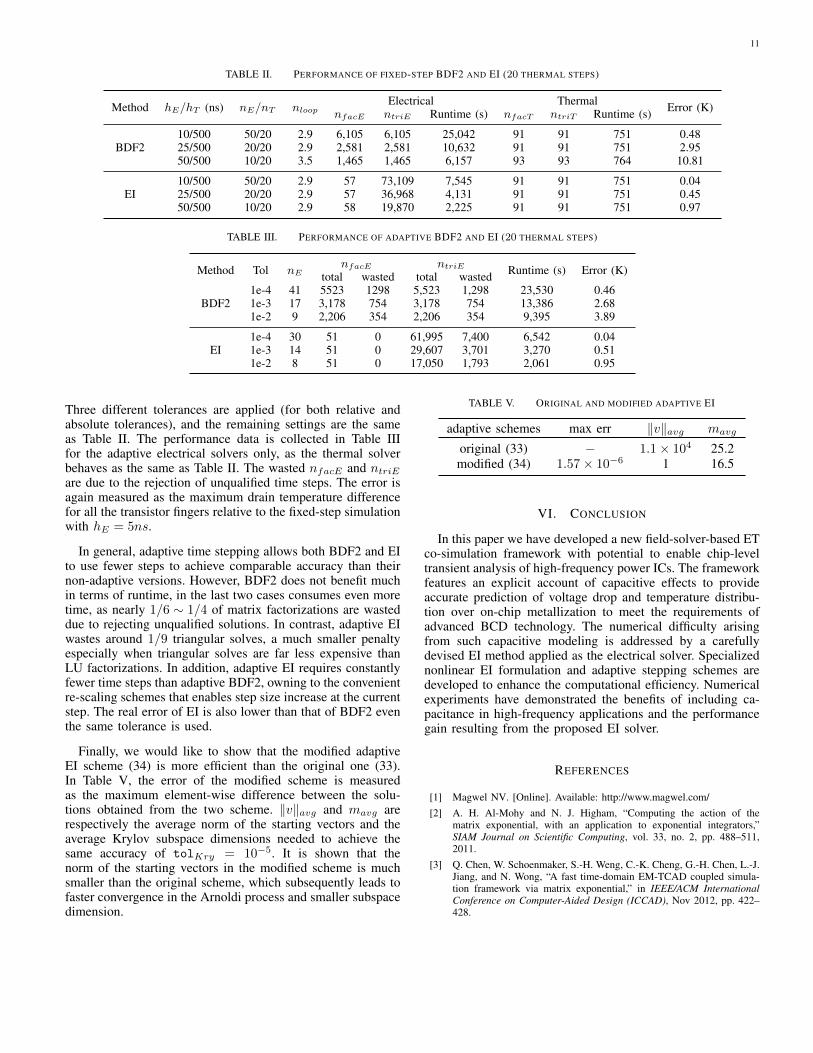
TABLE II. PERFORMANCE OF FIXED-STEP BDF2 AND EI (20 THERMAL STEPS)
Method hE/hT (ns) nE/nT nloopElectrical Thermal Error (K)
nfacE ntriE Runtime (s) nfacT ntriT Runtime (s)
BDF210/500 50/20 2.9 6,105 6,105 25,042 91 91 751 0.4825/500 20/20 2.9 2,581 2,581 10,632 91 91 751 2.9550/500 10/20 3.5 1,465 1,465 6,157 93 93 764 10.81
EI10/500 50/20 2.9 57 73,109 7,545 91 91 751 0.0425/500 20/20 2.9 57 36,968 4,131 91 91 751 0.4550/500 10/20 2.9 58 19,870 2,225 91 91 751 0.97
TABLE III. PERFORMANCE OF ADAPTIVE BDF2 AND EI (20 THERMAL STEPS)
Method Tol nEnfacE ntriE Runtime (s) Error (K)total wasted total wasted
BDF21e-4 41 5523 1298 5,523 1,298 23,530 0.461e-3 17 3,178 754 3,178 754 13,386 2.681e-2 9 2,206 354 2,206 354 9,395 3.89
EI1e-4 30 51 0 61,995 7,400 6,542 0.041e-3 14 51 0 29,607 3,701 3,270 0.511e-2 8 51 0 17,050 1,793 2,061 0.95
Three different tolerances are applied (for both relative andabsolute tolerances), and the remaining settings are the sameas Table II. The performance data is collected in Table IIIfor the adaptive electrical solvers only, as the thermal solverbehaves as the same as Table II. The wasted nfacE and ntriEare due to the rejection of unqualified time steps. The error isagain measured as the maximum drain temperature differencefor all the transistor fingers relative to the fixed-step simulationwith hE = 5ns.
In general, adaptive time stepping allows both BDF2 and EIto use fewer steps to achieve comparable accuracy than theirnon-adaptive versions. However, BDF2 does not benefit muchin terms of runtime, in the last two cases consumes even moretime, as nearly 1/6 ∼ 1/4 of matrix factorizations are wasteddue to rejecting unqualified solutions. In contrast, adaptive EIwastes around 1/9 triangular solves, a much smaller penaltyespecially when triangular solves are far less expensive thanLU factorizations. In addition, adaptive EI requires constantlyfewer time steps than adaptive BDF2, owning to the convenientre-scaling schemes that enables step size increase at the currentstep. The real error of EI is also lower than that of BDF2 eventhe same tolerance is used.
Finally, we would like to show that the modified adaptiveEI scheme (34) is more efficient than the original one (33).In Table V, the error of the modified scheme is measuredas the maximum element-wise difference between the solu-tions obtained from the two scheme. ‖v‖avg and mavg arerespectively the average norm of the starting vectors and theaverage Krylov subspace dimensions needed to achieve thesame accuracy of tolKry = 10−5. It is shown that thenorm of the starting vectors in the modified scheme is muchsmaller than the original scheme, which subsequently leads tofaster convergence in the Arnoldi process and smaller subspacedimension.
TABLE V. ORIGINAL AND MODIFIED ADAPTIVE EI
adaptive schemes max err ‖v‖avg mavg
original (33) − 1.1× 10⁴ 25.2modified (34) 1.57× 10⁻⁶ 1 16.5
VI. CONCLUSION
In this paper we have developed a new field-solver-based ETco-simulation framework with potential to enable chip-leveltransient analysis of high-frequency power ICs. The frameworkfeatures an explicit account of capacitive effects to provideaccurate prediction of voltage drop and temperature distribu-tion over on-chip metallization to meet the requirements ofadvanced BCD technology. The numerical difficulty arisingfrom such capacitive modeling is addressed by a carefullydevised EI method applied as the electrical solver. Specializednonlinear EI formulation and adaptive stepping schemes aredeveloped to enhance the computational efficiency. Numericalexperiments have demonstrated the benefits of including ca-pacitance in high-frequency applications and the performancegain resulting from the proposed EI solver.
REFERENCES
[1] Magwel NV. [Online]. Available: http://www.magwel.com/[2] A. H. Al-Mohy and N. J. Higham, “Computing the action of the
matrix exponential, with an application to exponential integrators,”SIAM Journal on Scientific Computing, vol. 33, no. 2, pp. 488–511,2011.
[3] Q. Chen, W. Schoenmaker, S.-H. Weng, C.-K. Cheng, G.-H. Chen, L.-J.Jiang, and N. Wong, “A fast time-domain EM-TCAD coupled simula-tion framework via matrix exponential,” in IEEE/ACM InternationalConference on Computer-Aided Design (ICCAD), Nov 2012, pp. 422–428.
12
[4] Q. Chen, W. Zhao, and N. Wong, “Efficient matrix exponential methodbased on extended Krylov subspace for transient simulation of large-scale linear circuits,” in Design Automation Conference (ASP-DAC),2014 19th Asia and South Pacific, Jan 2014, pp. 262–266.
[5] S. Cox and P. Matthews, “Exponential time differencing for stiffsystems,” Journal of Computational Physics, vol. 176, no. 2, pp. 430–455, 2002.
[6] Freescale, “Freescale Semiconductor’s MET LDMOS model,” 2000.[7] R. Gillon, P. Joris, H. Oprins, B. Vandevelde, A. Srinivasan, and
R. Chandra, “Practical chip-centric electro-thermal simulations,” in 14thInternational Workshop on Thermal Inveatigation of ICs and Systems(THERMINIC), Sep 2008, pp. 220–223.
[8] A. Irace, G. Breglio, and P. Spirito, “New developments of THER-MOS3, a tool for 3D electro-thermal simulation of smart power MOS-FETs,” European Symposium on Reliability of Electron Devices, FailurePhysics and Analysis, vol. 47, pp. 1696 – 1700, 2007.
[9] Q. Mei, N. Wong, and Q. Chen, “A chip-level transient electro-thermalfield simulator with gate capacitance and matrix exponential,” in IEEEIntl. Conf. on Solid-State and Integrated Circuit Technology (ICSICT),Oct 2014, pp. 1–4.
[10] C. Moler and C. V. Loan, “Nineteen dubious ways to compute theexponential of a matrix,” SIAM Review, vol. 20, pp. 801–836, 1978.
[11] ——, “Nineteen dubious ways to compute the exponential of a matrix,twenty-five years later,” SIAM Review, vol. 45, no. 1, pp. 3–49, 2003.
[12] Q. Nie, Y.-T. Zhang, and R. Zhao, “Efficient semi-implicit schemes forstiff systems,” Journal of Computational Physics, vol. 214, pp. 521–537,2006.
[13] M. Pfost, C. Boianceanu, H. Lohmeyer, and M. Stecher, “Electrothermalsimulation of self-heating in DMOS transistors up to thermal runaway,”IEEE Trans. Electron Devices, vol. 60, no. 2, pp. 699–707, Feb 2013.
[14] M. Pfost, D. Costachescu, A. Mayerhofer, M. Stecher, S. Bychikhin,D. Pogany, and E. Gornik, “Accurate temperature measurements ofDMOS power transistors up to thermal runaway by small embeddedsensors,” IEEE Transactions on Semiconductor Manufacturing, vol. 25,no. 3, pp. 294–302, Aug 2012.
[15] W. Schoenmaker, O. Dupuis, B. De Smedt, P. Meuns, J. Ocenasek,W. Verhaegen, D. Dumlugol, and M. Pfost, “Fully-coupled 3D electro-thermal field simulator for chip-level analysis of power devices,” in 19thInternational Workshop on Thermal Investigations of ICs and Systems(THERMINIC), Sep 2013, pp. 210–215.
[16] S. Theeuwen and H. Mollee, “LDMOS transistors in power microwaveapplications,” dec. white paper at Micr. Journ. web, 2008.
[17] S.-H. Weng, Q. Chen, and C.-K. Cheng, “Time-domain analysis oflarge-scale circuits by matrix exponential method with adaptive control,”IEEE Trans. Comput.-Aided Design, vol. 31, no. 8, pp. 1180–1193,2012.
[18] S.-H. Weng, Q. Chen, N. Wong, and C.-K. Cheng, “Circuit simulationvia matrix exponential method for stiffness handling and parallel pro-cessing,” in IEEE/ACM International Conference on Computer-AidedDesign (ICCAD), Nov 2012, pp. 407–414.
[19] H. Zhuang, S.-H. Weng, and C.-K. Cheng, “Power grid simulation usingmatrix exponential method with rational Krylov subspaces,” in IEEE 9thInternational Conference on ASIC (ASICON), Oct 2013, pp. 369–372.
[20] H. Zhuang, S.-H. Weng, J.-H. Lin, and C.-K. Cheng, “MATEX: Adistributed framework for transient simulation of power distributionnetworks,” in IEEE/ACM Design Automation Conference (DAC), 2014,pp. 81:1–81:6.
[21] H. Zhuang, W. Yu, S.-H. Weng, I. Kang, J.-H. Lin, X. Zhang,R. Coutts, J. Lu, and C.-K. Cheng, “Simulation algorithmswith exponential integration for time-domain analysis of large-scale power delivery networks,” ArXiv, 2015. [Online]. Available:http://arxiv.org/abs/1505.06699