1% 6b\ futurebus+1 cdirm - google compute engine
TRANSCRIPT
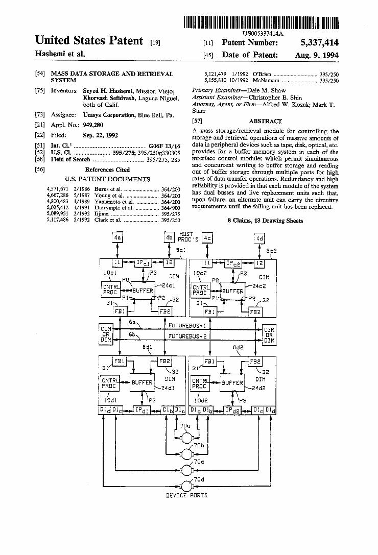
United States Patent [191 Hashemi et a1.
[54] MASS DATA STORAGE AND RETRIEVAL SYSTEM
[75] Inventors: Seyed H. Hashemi, Mission Viejo; Khorvash Sefidvash, Laguna Niguel,
USOO5337414A
[11] Patent Number: 5,337,414 [45] Date of Patent: Aug. 9, 1994
5,121,479 1/1992 O’Brien .................. 395/250 5,155,810 10/1992 McNamara ....................... .. 395/250
Primary Examiner-Dale M. Shaw Assistant Examiner-Christopher B. Shin
both of Calif. Attorney, Agent, or Firm-Alfred W. Kozak; Mark T. Starr
[73] Assignee: Unisys Corporation, Blue Bell, Pa. [57] ABSTRACT
[21] Appl. No.: 949,280 _ _ _ A mass storage/retneval module for controlling the
[22] Flledi SeP- 22, 1992 storage and retrieval operations'of massive amounts of [51] Int. 01.5 ............................................ .. G06F 13/16 data in Peripheral devices Such as tape’ disk’ Optical, etc‘ [52] Us. (:1. ..................... .. 395/275; 395/250g330305 Provides for a buffer memory System in each of the [58] Field of Search .............................. .. 395/275, 285 interface control modules which permit Simultaneous
_ and concurrent writing to buffer storage and reading [56] References Clted out of buffer storage through multiple ports for high
Us PATENT DOCUMENTS rates of data transfer operations. Redundancy and high reliability is provided in that each module of the system
Bums Ct ....................... .. has dual busses and live replacement units Such that’ 4,667,286 5/1987 Young et a1. . . . . . . . . . . .. 364/200 . . . .
4 800 483 V1989 Yamamoto et al 364/200 upon failure, an alternate unlt can carry the circuitry 5:O25:412 V1991 Dalrymple et a1: 364/900 requirements until the failing unit has been replaced. 5,089,951 2/1992 Iijima ........... .. .. 395/275
5,117,486 5/1992 Clark et a1. ................ .. 395/250 8 Claims, 13 Drawing Sheets
HUS T . FREE '3 4C [40
851 8:2 1 MM ' 11 1 [Ocl P3 10:2 P3
.1 \ Pck / E41:111 \ P0 / aim , /- c r24: EQEEL BUFFER gggiéLwisul-Tza ‘———P1 ‘P2 P1~ . (“P2
31 T 32 31 32 3 PB 1 —[ FB 2 F B 1 FB 2
\ 1 so A l I
1% 6b\ FUTUREBUS+1 CDIRM IDIM \ FUTUREBUS+2 ‘DIM
Bdl 8d2 i \ r v \ 1
1' ?ll-1 [123%] F51 31 v I 32 31 , 3a
CNTR DIM cNTRI BUFFER DI" i PRUC BUFFER \24d1 PRUC \24d2
:' / \ f A \ 10:11 P3 10:12 , P3
Dld’DTcFJ IPdl MDIbIDIQ 111Q]n1b|_,| IPGEHDICIDIG 11 A 1 1 11
101 1
gob 70a
7
1270s DEVICE PORTS


US. Patent Aug. 9, 1994 Sheet 2 of 13 5,337,414
CIM CHANNEL INTERFACE MUDULE
8_c_
I DIM
DEVICE INTERFACE MEIDULE
gg
F I G . 1 B

US. Patent Aug. 9, 1994 Sheet 4 of 13 5,337,414
Bal
PDRT 2A PDRT 3A ADDRESS ADDRESS
PDRT DA PDRT 1A ADDRESS ADDRESS
ADDRESS VLSI
B02
ET. ET. @v RV
E m "M
Baa.‘ T' U E
.L a U H
D24? + T. M L
V m
E A
w. .m 0
D14“ '. D 2
M E
D04‘ T U E
M
Bda
PDRT 3D <._. DATA
SEE FIG. PDRT DD PDRT 1D
DATA DATA PDRT ED DATA
FIG.3

US. Patent Aug. 9, 1994 Sheet 6 of 13 5,337,414
_1 _ _ _ _~ _ _ _
E
u m EH2 " n m on: n n 9 as: u “ 0 E2 0
So $55? “.325: m: 0:
‘ll
Q3“ 35 wwmmam
m VS: _ x3: ¢m EE <m E5 3 EE <0 Ema
:vm
mu J S35
7: 3592 E5 \ L "1! "Hi" B .
2a PW.“ "1W 1W row“ m u H u

US. Patent Aug. 9, 1994 Sheet 7 of 13 5,337,414
BI I/E]
24dw READ DATA
BI I/U
BI I/U
PORT 31]
BI I/U
PERT 2D
BI I/D
24dr
I/“w 1/249 BI I/U
\JRITE DATA
A A
BI I/U
PURT 11)
BI I/El
PORT OD
I
P2 P1 P0
F'IG.6

US. Patent Aug. 9, 1994 Sheet 9 of 13 5,337,414
@SHDVS THE PDRT EDNNEETED TD \JHICH MODULE
[MDDULE D] EHJDULE U IMUDULE 2| ‘MODULE. 3] FIG.8
READj INC H IDLE 1
[PDRT HDRHE I-VgzéEésZT-F IDiLE H 11in: J IPEIRT H INC H vRITE WKIZJZZXZZH IDLE j
@DRT 3]—-{ REM] H Irllc H IDILE W FIG . 8A FIRST SYSTEM CYCLE
TMDDDLE g WDDULE 1| {MDDDLE 2T [MDDuLEg
TRDRTg-A IDLE READ H INC J
FPDRT 1H Irlqc H vRITE ygzz, IDILE ] TRDRT 2W IDILE F Irlqc H vRITE Wgzm TPDRT H?zkzA-Fmln H Irlqc H IDlLE ] FIG.8B SECDND SYSTEM CYCLE
IMUDULE 0T WDDDLE 1] TMDDDLE 21U1DDULE a]
[RDRI DH INC J-FIDLE W 3,24 READ 1 l L
NC vRITE "'"rrA TPDRI 1l—-F IDILE T-F II }-F I IPDRT EPWZZEQZi-T IDLE j-F INC j \JRITEJ
l l l
[RDRT 3H IDLE kwgtiw READ H’ INC J FIG.8C THIRD SYSTEM CYCLE
IMEIDULE D1 FMDDDLE ll TMDDDLE ll IMEIDULE 3] I i V T IPURT 0H READ J-T I211: T-F IDILEJWEI’EZXA
IDlLE j II;1C J-EVRITEI FDRIHVRIIE IDILE J-E IIIIC ] [PDRT 3H INC J-F IDLE ?aw/3T READ J FIG.8B SECUND SYSTEM CYCLE


US. Patent Aug. 9, 1994 Sheet 11 of 13 5,337,414
@SHUVS PERT 0 DDNNEETED TD MDDuLE [24MB 24ml <01: F100) 24m2£4n31 TIME MDDULE MDDDLE MUDULE MDDDLE
ADDRESS PERIDD 0 1 2 a
I + I I v ‘ I I [ [FINE 0->/ /,-[ IDLEH IDLE H IDLEJ
I ' I’ I t’ l I
RIDDBFEJ [TIME 1*»[90 ILAT AD LATHAD LAT] HIDDDEEJ [TIME EMT/MT [-[vAIT l l
[DDDBEEJ [TIME 3-»[I/AIT H vAITj \JAIT '/,,',5%% , ’ I’ l I
[0003E2[ [TIME 4 vAITT-[ \JAIT [FT/AIL] ' "I" l l
[0003E2[ [TIME s[—>[ IDLE VRITE H IDLEJ L
Wow-‘y [TIME s INC [-LIDLE
[0003E4l [TIME I l
T[->[ \JRITE H INC [-[ IDLE M" 74"? 44942449571. [0003E5J [TIME
' II’!!! I 1
DJ vRITEH IMI: [-FIDILEJ [DDDQEEJ TIME 9 IDLE j \JRITEH INC [
[00031-1 [TIME 10 IMI: H IDLE
[0003Fg[ [TIME 15% vRITE [-[ Iilc H IDILE [0003E9[[TIME 12 vRITEj INC HIDLEJ
[OOO3FA [TIME 13 IDILE DRITEJ-FIMD J [0003ED[ [TIME IN 1M0 H IDILE
[0003FDHTIME 15 vRITEj IiNc [-FIDJLE [00031-‘0 [TIME 16 £25533 \JRITE H IMEJ-FIDILE [
[DDDDEEJ WIME ITHIDILE vRITEJ-FINI: [ [0003EE] [TIME I0-~[ INcj IDLE
[000400[ [TIME 19 vRITE H Iéxc H IDILE I BUSY [ [TIME 20 IDLE H IDILE H IDILE [ [ J [TIME EHIDLE IDLEJ-TIDLEJ
‘SYSTEM‘ CYCLE FIG.1O
US. Patent
R'l\ OPERATION
HOST SENDS A COMMAND FOR A READ
TO CIM
T
Aug. 9, 1994 Sheet 12 0f 13
R-B/
PROTOCOL ,
CHIP 1 I SENDS THE COMMAND TO INTERFACE CONTROLLER IPC
T
R-B/
IPC TRANSFERS THE COMMAND TO THE BUFFER 24
5,337,414
FIG._11
———T DRIVE 70 SENDS DATA
TO BUFFER 24D VIA D1 8; IPD
T CONTROL PROCESSOR
THE STATUS
T
AND STATUS /R-7
10D CHECKS \-R'8
I !
CONTROL PROCESSOR 1D SENDS THE COMMAND THRU FBI [31 1 TO
CONTROL PROCESSOR 10D SENDS DATA 8| STATUS TO CIM THRU FBE [38]
T DIM
L
R-S/ ‘FBI [31 1 IN DIM TRANSFERS THE COMMAND TO THE BUFFER
FEB [32] IN CIM SENDS THE DATA 8; STATUS TO BUFFER 24C
T 24
T
R-e/
CONTROL PROCESSOR 10D SENDS A COMMAND TO DRIVE 70 THRU IPD AND D1
CONTROL PROCESSOR 10C SENDS DATA 8: STATUS FROM BUFFER TO IPC
T___L
T IPC SENDS DATA AND STATUS TO
TilOST 4 VIA 1
,- R-lE

US. Patent Aug. 9, 1994 Sheet 13 of 13 5,337,414
HDST SENDS F I G _ 1 2 A DDMMAND
v-1 FDR A URITE \ DPERATIDN
VITH DATA —I TD CIM
DRIvE 70 I vRITES DATA
BBBB'B W cHIP I1 SENDS BUFFER 24D THE EDNNAND VIA D1 8' IPD
v-a/ AND DATA TD INTERFACE I CUNTREILLER IPC
CUNTRUL + A PRDEESSDR \_V 8
IPC TRANSFERS ?g THE CUMMAND V_3/ AND DATA TU ;
THE BUFFER 24 EDNTRDL
+ PRDEESSDR , \ CUNTRUL 10D SENDS v 9
STATUS TD CIM PRUCESSDR 10c THRU FEB [32] SENDS THE DATA
\1-4/ AND EDMHAND I THRU FBI [31] TD DIM FBB [32] IN
CIM SENDS + THE STATUS, \\I—10
H31 #31 ] PETERS TD BUFFER 24c DIM ANS
V"5/ THE EDMNAND + AND DATA TD “ CUNTRDL BUFFER 24 PRUCESSUR _
10C SENDS _\\}-11
* “AI-ES §Em£P¢ U CUNTRUL B F R PRUCESSEIR +
V_6/ 10D SENDS EDNMAND AND IPC SENDS W12 DATA TD DRIVE STATUS TD /' 70 THRU IPD HDST 4 MA AND D1 11

5,337,414 1
MASS DATA STORAGE AND RETRIEVAL SYSTEM
FIELD OF THE INVENTION
This disclosure involves control systems providing con?gurations for mass storage using various types of peripherals such as disk, tape or optical drives.
CROSS REFERENCES TO RELATED APPLICATIONS
This application is related to co-pending applications U.S. Ser. No. 898,633 ?led Jun. 15, 1992 entitled Uni versal Power Distribution System, and US. Ser. No. 948,381 ?led Sep. 21, 1992 entitled “Multiported Buffer Memory System for Disk Drive Complex” which appli cations are included herein by reference.
BACKGROUND OF THE INVENTION
Continued development and upgrading of magnetic disk subsystems lead to the desirable features of higher performance, greater capacity, higher reliability, more connectivity, in addition to reduced power consump tion, reduced footprint area, and reduced heat dissipa tion. As seen in FIG. 1B, the general block diagram of the
present mass storage and retrieval system would include a host processor 4 for several interface modules such as channel interface module 8, (CIM) and device interface module 8,1 (DIM) connected to a plurality of disk drive units 70 or other types of peripheral storage devices. The particular interfaces in various types of mass stor age systems will vary according to the individual design of the manufacturer. In the present described architec ture, the interfaces involve two particularly ef?cient interfaces known as the channel interface module 86 which uses the later described buffer memory of the mass storage system and also a device interface module (DIM) 8,1 which also uses the herein described buffer memory system con?guration.
In the prior art and other conventional memory sys tems, where buffer memories were used in interfaces for Read, Write, and other operations in mass storage sys tems, the requirement of time multiplexing of the mem ory caused undesirable wait periods for accessing by the numerous sources which had to access the memory. As an example, buffer memories would normally be
accessed by various sources such as a host processor, a control processor, and by various data channels which communicated to a series of peripheral storage units. It was the problem of delay and of waiting for taking of turns for each of these particular outlying sources in accessing the buffer memory, that created and caused unacceptable delays. When dual port buffer memories were used, this not
only increased the cost, the amount of board surface involved, but also increased power usage on the board in addition to causing contention between the two ports of each memory. Even in this case, there were two sources of access which still had to wait for their turn for memory access and attention.
In order to reduce the use of power consumption and to reduce the amount of board surface required and especially to keep the simplicity as well as the n“fairness of access” to all of the sources available, the present architecture for a storage and retrieval system provid ing massive data storage having rapid access and re trieval on a simultaneous and concurrent basis using
10
25
45
55
60
65
2 multiple peripheral storage devices, has been designed to overcome the aforementioned limitations. Further, redundancy of buses, power supplies and faulty module replacement without shutdown, allows uninterruptible access to stored information.
GENERAL OVERVIEW
A more highly ef?cient and less costly data storage and retrieval system for mass storage is indicated in FIG. 1B. FIG. 1A shows one-half of the overall system in order to illustrate the ?exibility and operability. A complete mass storage con?guration would include twice the number of CIM and DIM controller boards shown in FIG. 1A. As seen in FIG. 1A, there are four controller boards,
two of which (861, 862) are the channel interface module (CIM) controller boards which use a specialized mul tiported buffer, and there is also shown in FIG. 1A two device interface module (DIM) controller boards (8,11, 8,3) which also use the specialized multiported buffer. A fully con?gured system would have eight interface
controller boards so that in FIG. 1A there would be four channel interface module boards (CIM) and four device interface module (DIM) boards.
Within each of the eight controller boards (of which four are shown in FIG. 1A), there is seen the buffer memory systems 24,;1, 24d, and 24,11, and 24,12) wherein each of these buffer memory systems have four ports designated as P0, P1, P2, and P3. As will be described hereinafter, all the individual
memory modules used in the multiported buffer mem ory are single ported static RAMs which are cheaper yet more dense and smaller in terms of usable space than multiport static RAMs. The presently described mass data storage system
consists of a family of stand alone data storage systems. These are attachable to certain Unisys Corporation host systems by means of a ?ber channel interface and block MUX channel (BMC) and (IPI) intelligent peripheral interface or by an industry standard small computer systems interface (SCSI). Each individual sub-system is self-contained within a
single cabinet and may consist of a unit called a Control Module Rack (CMR) and from 1 to 8 Data Storage Racks (DSR) which may be any combination of mag netic disk, optical disk, cache memory, or even mag netic tape based storage units.
Various functional control module rack (CMR) con ?gurations permit any combination of Channel Inter~ face Modules (CIM) and Device Interface Modules (DIM), con?gured up to a maximum of 8 separate mod ules. A con?guration of 4 CIMs and 4 DIMs will provide
8 host ports and 16 SCSI buses. Data storage capacity (unformatted) for the “disk
only” version is expandable from a basic 2.3 gigabytes (single disk drive) to 128 gigabytes (56 dual ported disk drives con?gured with seven drives per dual SCSI bus.
Additionally, the disk-only option can be arranged to support a RAID technology which functions as a re dundant array of inexpensive disks. This can be done in the RAID space “0” (Simplex) and also in a RAID 3 and modi?ed RAID 5 (parallel array) con?guration. The presently described mass storage subsystem has
the capability for fully redundant operation and is pro vided with “live replacement” modules for all subsys tems such as the power system, power control system,

5,337,414 3
data channels and storage devices. This permits virtu ally uninterruptible access to stored information. Thus data loss in such a redundant con?guration is virtually eliminated. The CMR or Control Module Rack contains all the
hardware logic required to manage and control the data storage and the mass storage subsystem. The Control Module Rack is a fully self-contained rack module which holds the following modular components. (i) two power supplies (AC to DC); (ii) channel interface mod ules (CIM); (iii) device interface modules (DIM); (iv) Futurebus Central Arbiter Module, (two each); (v) Futurebus Backplane Assembly. A total of eight standard CIM and DIM modules can
be mounted in the Control Module Rack. The interface control logic modules designated as the
CIM and the DIM are located in the Control Module Rack and communicate with each other by means of the industry standard IEEE Futurebus Plus Interface. The CIM modules provide communication to the Host Sys tem via a ?ber channel interface using the federal stan dard F IPS 97 protocol (Federal Information Processing Standards Protocol), or BMC (Block Multiplexer Chan nel) or IPI (Intelligent Peripheral Interface) or via the industry standard SCSI interface. The device interface modules (DIM) provide control
and communication with the data storage devices in the Data Storage Rack (DSR) by means of the industry standard SCSI-2 Interface. All of the active compo nents and modules of the control module rack (CMR) are designed for live replacement together with full fault noti?cation to the host system to permit on-line maintenance capability. Power regulated DC power (for the CIM/DIM mod
ules located in the Control Module Rack) are provided by two AC-DC power converter modules. These power modules operate as a parallel redundant pair, normally sharing the power load of the Control Module Rack.
In the event of failure of either power module, the other power module automatically assumes the full load of the Control Module Rack until replacement of the faulty module can be affected. Failure information is also sent to the host system to alert it that module re placement is required. The “live replacement” capabil ity of the power modules assures that there will uninter rupted operation of the control module rack CMR in the event of a power module failure without need to shutdown the system. The Futurebus Backplane Assembly consists of two
32-bit wide, fully independent backplane data buses, each having associated Futurebus control bus lines. In the event of a fault on one of the buses, a control proces sor (in each CIM, DIM) will automatically recon?gure in order to utilize single bus operation and continue to operate even though in a reduced band width mode. Within the Channel Interface Module (CIM), there is provided a Fiber Channel Interface Module which pro vides communication with the host system by means of a ?ber channel interface. Two simultaneously usable channel connections are provided as standard operating functions. Communications with other channel inter face modules (CIM)and other device interface modules (DIM) within the mass storage subsystem is done using the industry standard Futurebus Interface.
In addition to providing host communication func tions, the CIM module also provides control and man agement of the Futurebus interface and management of
15
20
25
40
45
50
55
65
4 all commands issued through its ?ber channel interface. The connection between a host and a peripheral data storage device during execution of a command, is de ?ned as a “logical path”. A “logical path”, within the subsystem segment, con
sists of a CIM module and a DIM module, intercon nected by the Futurebus Backplane Assembly, and the connection from the Device Interface Module (DIM) to the peripheral storage devices via the SCSI-2 Interface Bus. An alternative or optional additive type of channel
interface module (CIM) is designated as the SCSI chan nel interface module. This module provides communi cation with the Host System 4 via the industry standard SCSI-2 interface. Two channel connections are pro vided as standard. Other functions of the SCSI-CIM are identical to that of the ?ber channel version of the chan nel interface module (CIM). The disk device interface module (DIM) provides
communication, in a RAID Simplex mode, with the data storage devices connected to the mass storage subsystem by using the industry standard SCSI-2 inter face. Four SCSI interface connections are provided as a standard. Communication with other CIM and DIM modules within the mass storage subsystem is done using the industry standard Futurebus Interface.
In addition to providing device communication func tions, the DIM module also provides control/manage ment of the Futurebus Interface and functions as a Host Adaptor and a SCSI Initiator for all received com mands. Each individual Disk Device Interface Module (DIM) can function as a magnetic disk control or as an optical disk control. The functional characteristics in volved are determined by the DIM microcode, which is downloadable from the Host System via a CIM/ Futurebus connection. One con?guration of the device interface module
(DIM) is designated as the RAID device module which provides communication, in a RAID 3 or modi?ed RAID 5 mode, with magnetic disk data storage devices within the subsystem by means of the industry standard SCSI-2 interface. The use of the RAID-DIMs require additional space
within the control module rack (CMR) above the space required for a standard device interface module (DIM). The Data Storage Rack (DSR) or Disk Data Storage
Rack contains all the hardware required for installation and support of a disk type data storage module in the subsystem. The control module rack (CMR) is a fully self-contained rack module which consists of the fol lowing components: (i) two power supplies; (ii) mag netic disk data modules (MDM) which may involve from 1 to 7 units; (iii) optical disk data modules (ODM), one, two, or four, depending on size; (iv) a SCSI-2 bus backplane assembly. A total of 7 MDM or ODM modules in any combina
tion can be mounted in the data storage rack (DSR). The Data Modules (MDM and ODM) in the data
storage module (DSR) communicate with the DIMs in the control module racks (CMR) by means of the indus try standard SCSI-2 interface. Each Data Module has dual SCSI-2 ports and can communicate with two DIM modules via dual SCSI-2 buses. Two fully independent SCSI-2 Bus subsystems are
implemented within each data storage rack DSR. Regu lated DC power is provided by redundant power supplies to all the data modules in the data storage rack. Again, all active components and modules are designed

5,337,414 5
for live replacement without shutdown with full fault noti?cation to the host system to permit on-line mainte nance capability. The SCSI-2 Bus Backplane Assembly (SBA) consists
of the printed circuit type of backplane having two SCSI-2 buses and a power distribution bus. In event of a fault on one of the SCSI-2 interface buses, a control processor in each CIM and DIM module automatically recon?gures that bus pair for single port operation and continues to operate in a reduced capability mode. The SCSI-2 bus interfaces are contained within the data storage rack (DSR). The Magnetic Disk Data Storage Module (MDM)
consists of one 5% or 3% inch extended form factor, dual ported SCSI-2 magnetic disk drive. This drive module is physically and electrically con?gured for “live inser tion” into the SCSI Bus Interface Module Backplane. No cables are required. Up to 7 data storage modules may be installed in a data storage rack (DSR).
Using 8 data storage racks this would provide a total of 56 magnetic disk storage modules for a full con?gura tion. This live replacement capability of a data storage module assures uninterrupted operation of a data stor age rack in the event a module must be replaced. The power distribution module (PDM) of the system
consists of dual independent Power Distribution Units (PDU) which are mountable or removable within the cabinet. The PDM has two independent AC Power Input Cables, one for each power distribution unit (PDU). Remote power sequencing and emergency power-off
capability (in accordance with FIPS 61) is also pro vided for the data storage rack (DSR). All active com ponents in the power distribution module (PDM) have live replacement capability together with full fault noti ?cation to the host system for uninterrupted operation. The Power Distribution Unit (PDU) provides con
trol, fault monitoring and distribution of AC Power to the various modules within the cabinet. Regulated DC power and also low voltage AC power for the control unit and FIPS-61 modules are also provided. In the event of failure of either power distribution unit (PDU), then the other PDU will automatically assume the full load of this subsystem until replacement of the faulty module can be effectuated. This live replacement capa bility assures uninterrupted operation in the event of a power component failure. Each PDU has a Control Module which provides sequence control functions and fault monitoring for the power distribution unit (PDU).
In the presently described embodiment, the buffer memory system is provided with four ports of 36-bits data width. Each and every one of the ports can access the entire memory in each of the memory modules of the buffer memory system.
Operationally the maximum wait period for any ?rst access is 350 nanoseconds and then the access to the next following data words will be operable at 80 mega bytes per second for the entire burst size. The burst size can be from one word to a maximum of the entire size of the memory system modules which is 64 megabytes. With the use of a multiport memory system in which
the described embodiment of FIG. 1A shows four ports, the information in the buffer memory system is shared between a control processor (1061, 1062, 10,11, 10,12) and two Future bus interfaces 31, 32 (FBI, FB2) plus the interface processors such as IP61, IP62, IPdI, IP42) which respectively provide interfaces to the host computer
25
5
45
55
65
6 and to the device interfaces for the multiple peripheral storage devices. As seen in FIG. 2, the buffer memory system is
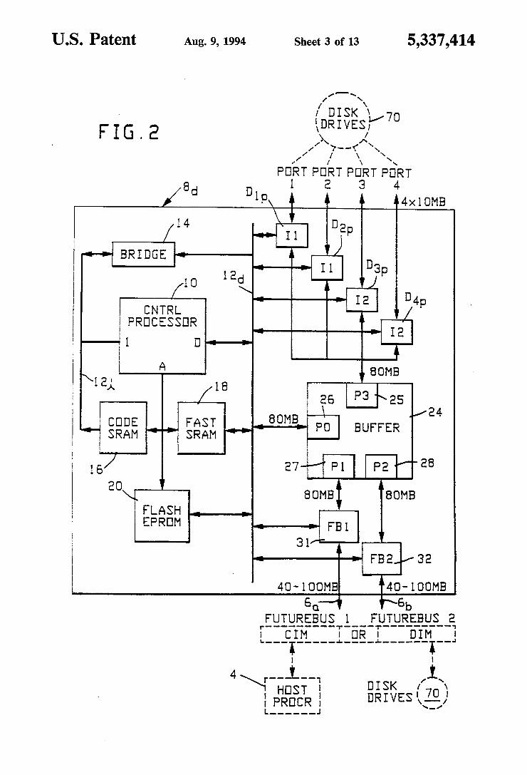
shown in more detail in conjunction with one controller board that is to say, the DIM device interface module controller board 8d. Each of the ports P0, P1, P2, P3 of FIG. 2 (26, 27, 28, 25) has a transfer capability of 80 megabytes per second. FIG. 3 shows a block diagram of the internal elements of the buffer memory system. The use of address-transfer VLSI circuits (24a) and data transfer VLSI circuits (244) are operable to reduce the power requirements of the system as well as the amount of board space and cost. Each of the ports P0, P1, P2, and P3 is capable of
handling 27-bits of Address Bus, 36-bits of Data Bus, and 6-bits of Control Bus. There are four memory modules in FIG. 3 (24m(),
24m, 24mg, 24m3) which are addressed with the least signi?cant bits of port addresses such that module 0 will hold all addresses ending in 00, module 1 will hold all addresses ending in 01 and module 2 will hold all ad dresses ending with 10 and module 4 will hold all ad dresses ending in 11. The buffer memory system interconnections are
shown in FIG. 4 where each memory module is seen to be connected to a port no matter what the status is of that port. This provides for equal access (fairness) to all ports within four system cycles wherein each system cycle takes a period of 50 nanoseconds. FIG. 5 shows the Address Transfer Logic (V LSI)
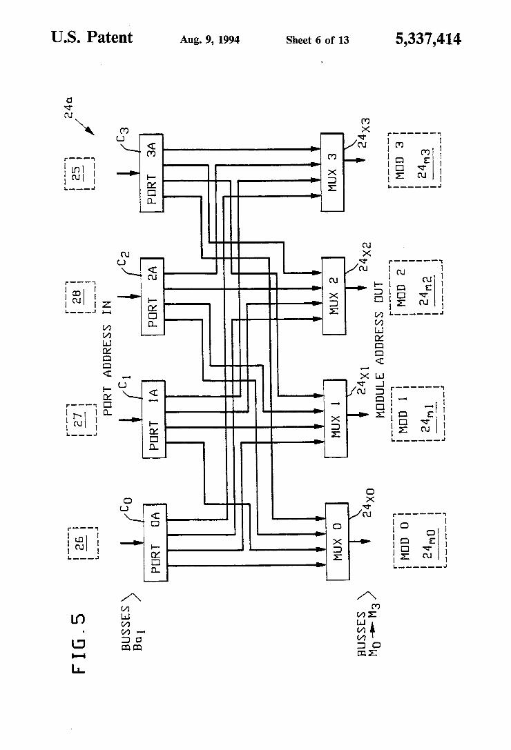
portion 24,, of the buffer memory system. It is seen that the address of each port is kept separately in a counter (C0, C1, C2, C3) which will then multiplex this address into each of the other module address ports. For one system cycle, the module addresses are all kept within each of the multiplexer units 24x0, 24x1, 24,2, 24x3) shown in FIG. 5. FIG. 6 shows the Data Transfer Logic portion
(VLSI) 24,1 of the buffer memory system. It will be noted that there are two independent paths for each port making it possible to individually read or to write simultaneously into the buffer at the same time. Each one of the bus interface input/output units (24,,
24,-) (BI-I/O) will be stable for at least one system cycle. Each memory module (24c, 244) is made up of four
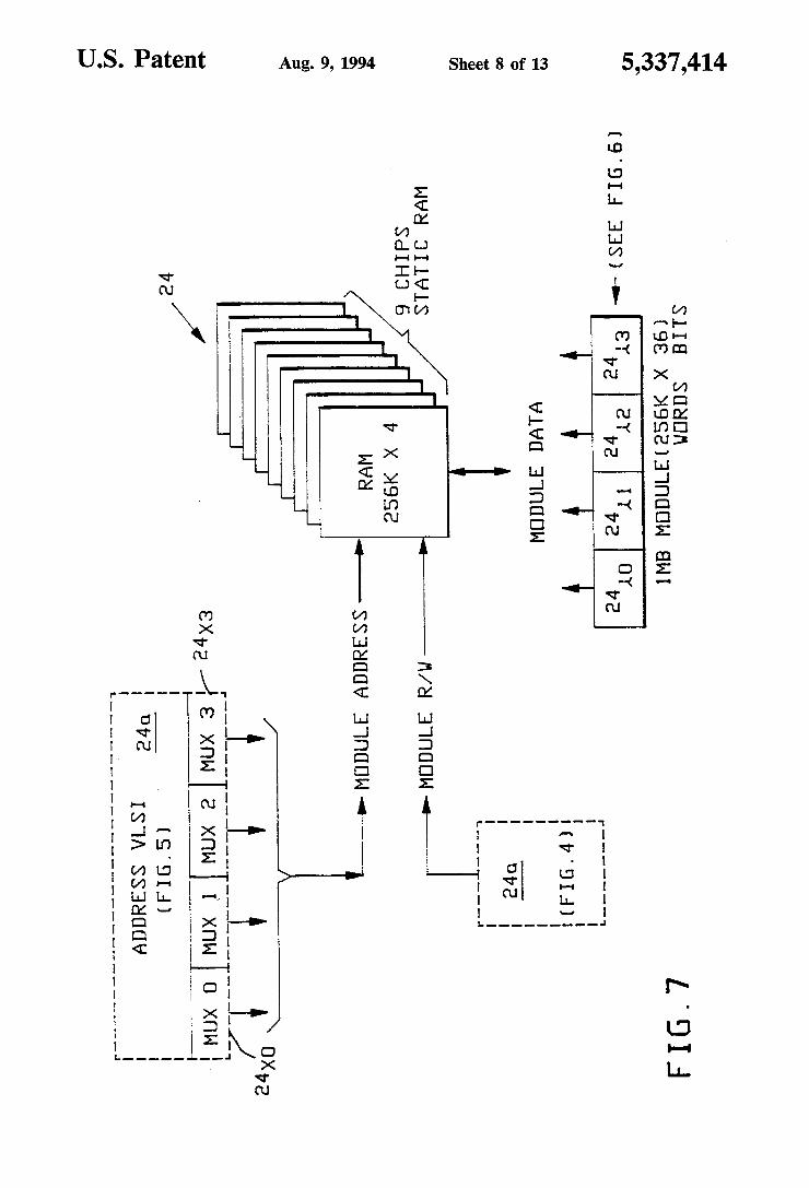
virtual module units constructed as shown in FIG. 7. To hold a capacity of four megabytes of 36-bit words, there are used nine static RAM chips, each of which is 256K><by 4 bytes. Thus the nine RAM chips provide 262,144 words of 36 bits each per virtual module for a total of 1,048,576 words of 36 bits each. Here, the 1,048,576 words of 36 bits each is the equivalent of 4,194,304 bytes (4 megabytes).
SUMMARY OF THE INVENTION
A single host computer or multiple numbers of host computers may be connected to control module inter faces which permit high speed storage of masses of data on various types of peripherals such as disk drives, optical drives and/or tape drives. The control module interfaces include a channel in
terface module (CIM) which interconnects to the host system for taking communications from the host system and transferring them across an internal bus to a periph eral device interface module (DIM). The peripheral device interface module (DIM) is
used to communicate between the physical data storage peripheral devices involved and the internal bus

5,337,414 7
(F uturebus) connecting the device interface module and the channel interface module (CIM). Each of the controller boards involving the channel
interface module (CIM) and the device interface mod ule (DIM) include high speed transfer multi-ported buffer units which permit the storage and transfer of data, both simultaneously on a Reading and Writing basis such that the multiple number of ports in a buffer memory system, within each controller board, permit access to a multiple number of memory modules in the buffer memory system. Thus within each one of the CIM and the DIM con
trol modules, the multi-ported buffer memory within each controller module permits simultaneous and con current writing storage of data while at the same time reading out of stored data. Within each of the buffer memory system modules (of which there are a multiple number M of modules), the system permits any one of the four input ports to the buffer memory system to access any one of the multiple number of memory mod ules within the buffer memory system for carrying out the functions of simultaneously reading out data and writing in data on a continuous basis. The mass data storage system is made up of a number
of individual subsystems where each subsystem is self contained within a single cabinet and this cabinet con sists of one Control Module Rack (CMR) and from one to eight Data Storage Racks (DSR) which house any combination of magnetic disk units, optical disk units, cache memory or magnetic tape base storage units. The subsystem is so arranged that it has the capability of fully redundant operation such that, during operations, it is possible to replace any module in any of the subsys tems without interrupting the data transfer operations or the access to the stored information. Thus data loss in such a redundant con?guration is practically elimi nated.
Additionally, a plurality of power supplies for the control module rack (CMR) is provided so that they operate as a parallel redundant pair of power supplies which share the power load. And in the event of failure of either module, the other power module will automat ically assume the full load of the control module rack (CMR) until replacement of the faulty module is effec tuated. .
The present invention also provides a large capacity buffer memory of four memory modules which permit exceedingly rapid transfer of data and simultaneously permit the Reading and Writing of data into and out of the memory modules from any one of the four ports of a multiport memory system.
In the preferred embodiment the multiport buffer memory system provides a port to a control processor, a port to a plurality of peripheral storage devices/or host computer, and two ports to buses which connect to other channel interface (CIM) and device interface (DIM) modules permitting data communication to and from a host processor and to and from a multiplicity of peripheral storage devices. The four ports of the buffer memory system are con
nected to an address transfer logic system which per mits access to each and every one of four memory mod ules in the system. Additionally a data transfer logic system connects to each one of the memory modules in order to permit the simultaneously Reading out of, and Writing into, of data words, while the four ports pro vide interface connection to a host system and also to a multiple set of peripheral storage modules.
20
25
30
35
45
50
55
60
65
8 System cycles are operative so that during any one
system cycle, there can be one access allowed from any port to any buffer memory module. However, while this one access is occurring on one system cycle, during the next system cycle there can be another access for either a Readout or a Write-in operation of a data word. The overall effect is that concurrently there is the con tinuous capability and ?ow of access to any one of the buffer memory modules from any one of the four ports of the buffer memory system. This insures an equality of access for each and every one of the ports to a desired buffer memory module and also insures that there can be simultaneous action cycles occurring both for the Read-out of data and for the Writing-in of data from any one of the multiple ports.
BRIEF DESCRIPTION OF THE DRAWINGS
FIG. 1A is a block diagram of a disk mass storage and retrieval system showing one-half of a typical system where there is seen two channel interface modules and two device interface modules which connect the host processors of the system to a plurality of disk drive modules. FIG. 1B is a simpli?ed block diagram of the overall
mass storage system. FIG. 2 is a diagram of the device interface module
and its internal usage of the multiported buffer memory system; FIG. 3 is a block diagram of the buffer memory sys
tem showing the various elements involved; FIG. 4 is a interconnecting diagram showing how the
buffer memory modules are interconnected to the four ports involved in the buffer memory system; FIG. 5 is a more detailed diagram of the address
transfer system of the buffer memory using buses and VLSI circuitry; FIG. 6 is a more detailed block diagram showing the
elements of the data transfer logic of the buffer memory system; FIG. 7 is a schematic drawing showing the arrange
ment of RAM chips to form the four-module buffer memory system; FIG. 8 is a drawing showing the relationship between
the four ports and the four buffer memory modules during each of a sequence of system cycles; FIG. 9 is a drawing showing the time sequence
wherein various addresses interact with the four mem ory modules of the buffer memory system in performing access-Read operations. FIG. 10 shows the access Write function during a
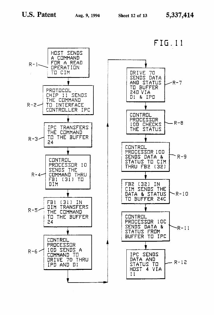
period of system cycles showing the relationship be tween the address, the time period involved and the various functions in each of the four memory modules; FIG. 11 is a flow chart showing the function of the
overall system during a Read and Status operation; FIG. 12 is a flow chart showing the various steps
involved in the system for a Write and Status operation.
DESCRIPTION OF PREFERRED EMBODIMENT
Referring to FIG. 1A there are shown four controller boards which are illustrative of one-half of the overall system. The normal system would have eight such con troller boards located in a single cabinet. As seen in FIG. 1A, the two upper controller boards
are modules designated as the channel interface module (CIM) and are shown as channel interface module 861 and 862.

5,337,414 The two lower controller boards are designated as
device interface modules (DIM) and are indicated as device interface modules 8,11 and 8,12.
Referring to the channel interface modules 861 and 862, there will be seen two protocol chips designated I-1 and I-2 which communicate to the main host processor 4 (or alternatively there can be communication to four separate host processors which could be designated 4”, 41,, 4c, and 4d). The protocol chips (I-1, I-2) can be desig nated as block multiplexer channel host interface proto col chips. These function to communicate data and to transfer commands and status information to and from the host processor 4. The ?rst set of protocol chips I-1 and L2 are under control of the interface processor designated IP61. The interface processor, IP61, controls the protocol chips L1 and L2 so that the interface pro cessor (IPcl) can independently act in order to provide an appropriate “fair share” of buffer access time to each one of the set of two protocol chips I-1 and L2.
Likewise, the interface processor IP62 is also a proces sor which operates as a hardware state machine and also provides the function to insure there will be a fair share of access time between the buffer 24¢; and each of the protocol chips I-1 and L2 in its communication to and from the host computer 4. The interface processor (such as IP01 and IPCZ) com
municates respectively to the buffer memories 2461 and 2462. These buffer memories are used to store informa tion data, control data, and status data during the opera tion of the system when data is being transferred be— tween the host computer 4 and a series of peripherals such as disk drive units 70a, 70b, 70c, 704. These disk units 70,, through 70d each represent multiple numbers of disk drive units. The buffer memory units 24C1 and 2402 are respec
tively controlled by the control processors 1081 and 103 which also monitor the dual busses 6a, 61, through state machines 31, 32 (FBI, FB2, FIGS. 1A, 2) for oper ability so that a malfunction in one bus will cause the control processor 10, FIG. 2, to channel data through the operable bus. As indicated in FIG. 1A, the buffer memory (such as
2461, 2462) will have four ports where the Port P1 con nects to the Futurebus state machine (F B1) 31; the Port P2 communicates with the second state machine FB2, 32; the third port P3 of the buffer memory 24 communi cates with the interface processor IP62 and the fourth port P0 communicates with the control processor 10:2. The Futurebus interface state machines (31,32) desig
nated FBI and FB2 function to communicate between the channel interface modules (8C1, 862) and the device interface modules (8,11, 8,12). The connective arrangements to the Futurebus inter
face state machines 31 and 32 are such that two sets of buses designated as 6,, and 61, will be seen to intercon nect the channel interface modules (CIM) with the device interface modules (DIM) in such a fashion that any channel interface module (CIM) can talk to anyone of the device interface modules (DIM) thru the Future bus state machines 31 and 32 (F B1 and FB2). Again referring to FIG. 1A, the lower control boards
8,11 and 8,}; are the device interface modules (DIM) which also have buffer memory units 24,11 and 244‘; respectively controlled by the control processors 10,11 and 10,12. The buffer memories 24,11 and 24d; will be seen to
have connections to the interface processors IPd1 and IPdz which are used to communicate with and handle
5
20
25
40
60
65
10 data transfer operations by means of device protocol chips D1 (D1, D11» D16, D1d,FIG. 1A). The device protocol chips, D1, are used to communicate to the disk drives 70“, 701,, 70c, and 70,11 in order to transfer com mands, data, and status information between the disk units 70 and the buffers 24,11 and 24,12. Likewise also the chips D1 (Dla, D15, D16, D1d,FIG. 1A) can be arranged to communicate with tape or optical disk storage means.
operationally, FIG. 1A illustrates how the host pro cessor system 4 can access information and data from the seven disk drives of 70(1 or the seven disk drives of 701,, or 70c or 70,1. The host 4 will send a command through the inter
face protocol chips such as I-1 or L2. The interface processor (IP61, IP62) will convey this command to the buffer memory (2401, 2462). The control processors 1061 or 10,; will execute the command and will send the command through the Futurebus state machines 31, 32 (such as FBl or FB2) to the device interface module (DIM) and its buffer memories (such as 24,11 and 24,12) for temporary storage. The control processor (such as processor 10,11 or
10,22) looks at the transmitted command from the host, and selects which one of the FIG. 1A device interfaces, D1, (D1,,, Dlb, D16, D14) of the device interface proto col chips will be used for access to send the command to a selected disk drive or other peripheral unit so that information can be accessed from the disk drive and returned through the device protocol interface D1 and into the DIM buffer 24,11 or 2442. The control processor (10,11 or 10,12) will transfer this data from the disk through the Futurebus state machines (31, 32) up to the CIM buffers (2401 or 2462). Then the interface processor (IP61, IP52) Will transfer this data up to the host system 4, thus completing the ?rst action of data transfer, which may be a READ operation or a WRITE opera tion. .
After this ?rst activity is completed, then the disk drives, such as 70,,, 701,, etc. will provide “status data” back to the host 4 through the same series of channel steps, that is to say, through the device protocol inter face, Dl, then through the interface processor IP41 then through the buffer 24,11, then through the Futurebus state machines 31, 32 of the DIM module 8,11, then by CIM module 8C1, via the buffer 2461 and to the interface processor IPcl and thence through the interface proto col chip (I-1 or L2) to the host system 4.
Referring to FIG. 2, there is seen a block diagram of the controller board 8,; on which is patterned on the device interface module, DIM (indicated as 841 and 8d2 of FIG. 1A). The control processor 10, FIG. 2, controls the execu
tion of commands received from the host 4 and operates upon the buffer memory 24. The control processor 10 is supported by the code SRAM 16 which provides mi crocode for the control processor 10 and is supported by the FAST SRAM 18 which provides a working scratchpad area for the processor 10. The FLASH EPROM 20 is a boot memory for starting up and for the diagnostic operations used by the processor 10. The control processor 10 has a data bus 12,; which
connects to the buffer memory 24, to the device proto col interfaces Dlp, D2p, D3p, D4p, and also to the Futurebus state machines 31 and 32, to sense any mal function in busses 6a, 61, and to re-direct communication through the properly operating bus. The device proto col interfaces Dla, D11,, D16, D1,; of FIG. 2 correlate to the interfaces D1 of FIG. 1A.
5,337,414 11
The bridge logic 14 (FIG. 2) is a group of logic gates used to connect the data bus 12,; and the instruction bus 12,". The DIM controller board 8 shown in FIG. 2 also
indicates that the buffer memory 24 of the DIM 8 has four basic input/output port areas shown as 27, 28, 25 and 26. (These correlate to ports P1, P2, P3, P0 of FIG. 1A). The interface ports 27 (P1) and 28 (P2) provide bus connections to the futurebus state machines 31 and 32. The buffer port interface 26 (P0) connects the control processor 10 via the data bus 12d, FIG. 2. The buffer port 25 connects the buffer memory 24 to the peripheral units via device protocol chips D1,, thru Dld, FIG. 1A to provide for channels of communication to the periph eral units 701,. The futurebus state machine 31 (FBI) connects
through the Futurebus-1 (designated, 64) to other chan nel interface modules (CIM). Likewise the Futurebus state machine 32 connects via the bus 61, in order to communicate to other device interface modules or DIMs. The control processor 10 of FIG. 2 may be imple
mented with an AMD 29000 RISC processor and is functionally used to control the channel interface mod ule (CIM) and the device interface module (DIM). The channel interface module 86 (CIM) is architectur
ally the same as the described DIM 8d of FIG. 2, except that instead of the 4 (quad) ports D1 (of D1“, Dlb, Dlc, D14, FIG. 1A the DIM), there are dual (2) ports in the protocol chips I1 and I2 for connection by each CIM board to the host processors of the host system 4.
FIG. 3 is a block diagram showing the elements of the buffer memory 24 previously discussed in FIG. 2. The buffer memory 24 has a ?rst portion block desig
nated as Address VLSI 24a. The Address VLSI block has 4 inputs from 4 address ports designated port 0A, port 1A, port 2A and port 3A which correspond, in FIG. 2, to the elements 26, 27, 28, and 25, and corre spond in FIG. 1A to ports P0, P1, P2, and P3. The Address VLSI module 24,, provides addressing
connections to the four memory modules 24mg, 24ml, 24,,,;, and 24m3. These modules are also designated as memory module 0, 1, 2, and 3, and are static RAMs which are generally designated as SRAM’s. Each of these static RAMs will hold 128K><36 bits of memory information.
Then, as noted in FIG. 3, there are a series of output two way data buses Bdl connecting each of the four static RAM modules to the Data VLSI module 24,]. The Data VLSI module 244 is made of two chips which perform the function of multiplexing data to the mem ory module. A series of data ports 0D, 1D, 2D, and 3D are provided to both take in and put out data to the Data VLSI module 24d. In FIG. 2 these four ports are desig nated as Dla, D15, Dlc, Dld and they provide for the interchange of data between the peripheral storage units (disk drives 70) and the buffer memory module 24. The incoming address buses in FIG. 3 are designated
B,,1 and each one of the four buses carries a 27 bit ad dress. The Address VLSI module 24,, which receives the data on the buses Bal is a module which is made of one VLSI chip which provides a multiplex function for simultaneously addressing the various memory modules such that any one of the address ports 0A, 1A, 2A, 3A, can operate to address each one of the four memory modules 0, 1, 2, 3. The addressing from the address module 24a is done by means of the address buses Bag.
15
25
45
60
65
12 Data which resides (FIG. 3) in the four memory
modules 0, 1, 2, and 3 (24mg, 24ml, 24m2, 24m3) is con nected by a set of data buses B41 to the data module 24d. These data buses enable data to be “written” into any one of the four memory modules or to be “Read out” from any one of the four memory modules on a simulta neous or concurrent basis. The data on any one of the data buses of FIG. 3 designated Bdg, can travel by means of the four ports 0D, 1D, 2D, 3D, which corre late to P0, P1, P2 and P3 of FIG. 2. The data buses B42 each carry 36 bits of data to or
from the memory modules 0, 1, 2, 3, for purposes of reading 36 bits of data or for writing in 36 bits of data. The four address ports 0A, 1A, 2A, 3A (also desig
nated as 26, 27, 28, and 25) receive the addresses from the control processor 10 such that any one or each one of the ports 0A, 1A, 2A, 3A, can address any one of the four memory modules 0, 1, 2, 3 (24m(), 24ml, 24mg, 24m3) concurrently in time.
In conjunction with the addressing of the various memory modules, it is also possible, at the same time, for data to be entering the ports 0D, 1D, 2D, and 3D (P0, P1, P2, P3) for purposes of writing into the particu lar sections of the addressed modules 0, 1, 2, and 3, of FIG. 3.
Likewise, concurrently data can also be being read out of the memory modules 0, 1, 2, and 3 and sent via the Data VLSI module 24dover to the data output ports 0D, 1D, 2D, 3D also designed P0, P1, P2 and P3 on FIGS. 2 and 3.
It should be understood, for example, that while port 2A is providing an address to the Address VLSI 24a, then at the same time, data can be entering for writing purposes on port 2D. For example, port P2(28), it should be understood, has two aspects, Le. 27 address lines (2A) and 36 data lines (2D).
It is possible for any one of the four ports 0A, 1A, 2A, 3A to address any one of the four memory modules 0, 1, 2, 3 concurrently and simultaneously while at the same time data is being written into or read from any particu lar ones of the memory modules 0, 1, 2, 3 by means of data transfers through the Data VLSI 24d. For example, each of the four ports 0D, 1D, 2D, and 3D can be writ ing to the same module, for example, as module 2, con currently, in order to write in data at separate or same locations in module 2 (24m2).
This is permissible since there can be four simulta~ neous addresses appearing on ports 0A, 1A, 2A, 3A, in order to tag or locate the special locations in module 2 where the writing of data is to be done. Another example of the buffer memory system ?exi
bility is that, for example, there may be two Reads and two Writes occurring at the same time involving each of the four memory modules 0, 1, 2, and 3, the only limitation being that each port 0A, (address) and port OD (data) information occur simultaneously. Similarly, the addressing through the port 2A to the memory module 2 (24m2) must be simultaneous with the data port 2D (28), holding the 36 bit data word.
It should be understood that each combination of “address” and “data” port is an independent operable entity. Thus, operationally, any port can access and address any location in any one of the four memory modules.
Likewise, any one of the data ports (0D, 1D, 2D, 3D) can access locations in any one of the four memory modules. The only limitation is that there be a “concur rence” in time between the port address information