080625 op-workshop csem-poe ho (cjw).ppt€¦ · polymer optoelectronics dr. carsten winnewisser...
TRANSCRIPT
Polymer OptoelectronicsDr. Carsten Winnewisser
Section Head Polymer OptoelectronicsCSEM Basel, 25.06.2008

O tliOutline
I t d ti t O i O t l t i• Introduction to Organic Optoelectronics
• Vapor phase depostion
Solution processed• Solution processed
• Applications
• OLED displays• OLED displays
• Illumination
• Signage• Signage
• Examples of Integrated Systems
• ConclusionConclusion
Copyright 2008 CSEM | POE | CJW | Page 1

CSEM locationsCSEM locations
CSEM Basel
CSEM Zürich
Headquarters CSEMNeuchâtelNeuchâtel
CSEM Alpnach
Copyright 2008 CSEM | POE | CJW | Page 2
O i O t l t i
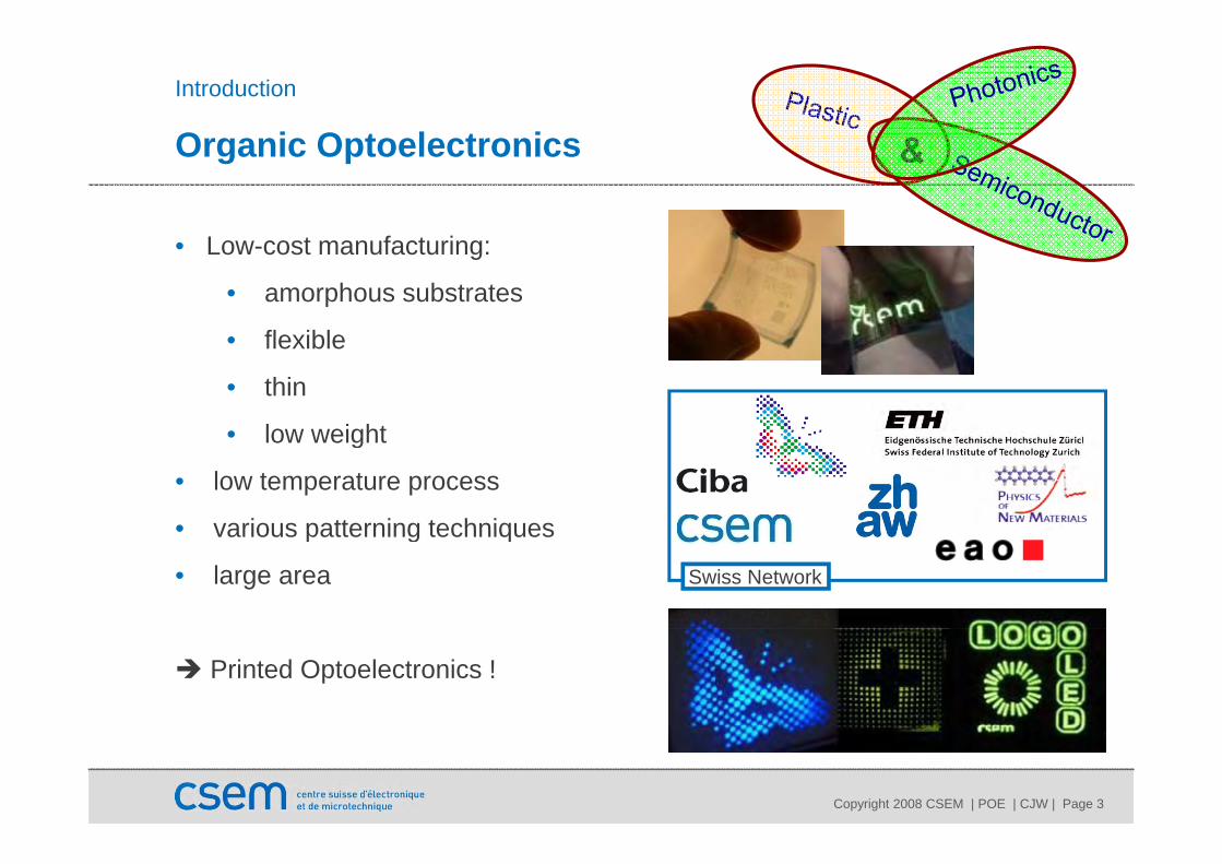
Introduction
Organic Optoelectronics
L f i• Low-cost manufacturing:
• amorphous substrates
fl ibl• flexible
• thin
• low weight• low weight
• low temperature process
• various patterning techniques• various patterning techniques
• large area Swiss Network
Printed Optoelectronics !
Copyright 2008 CSEM | POE | CJW | Page 3
Thi fil d iti t h l i
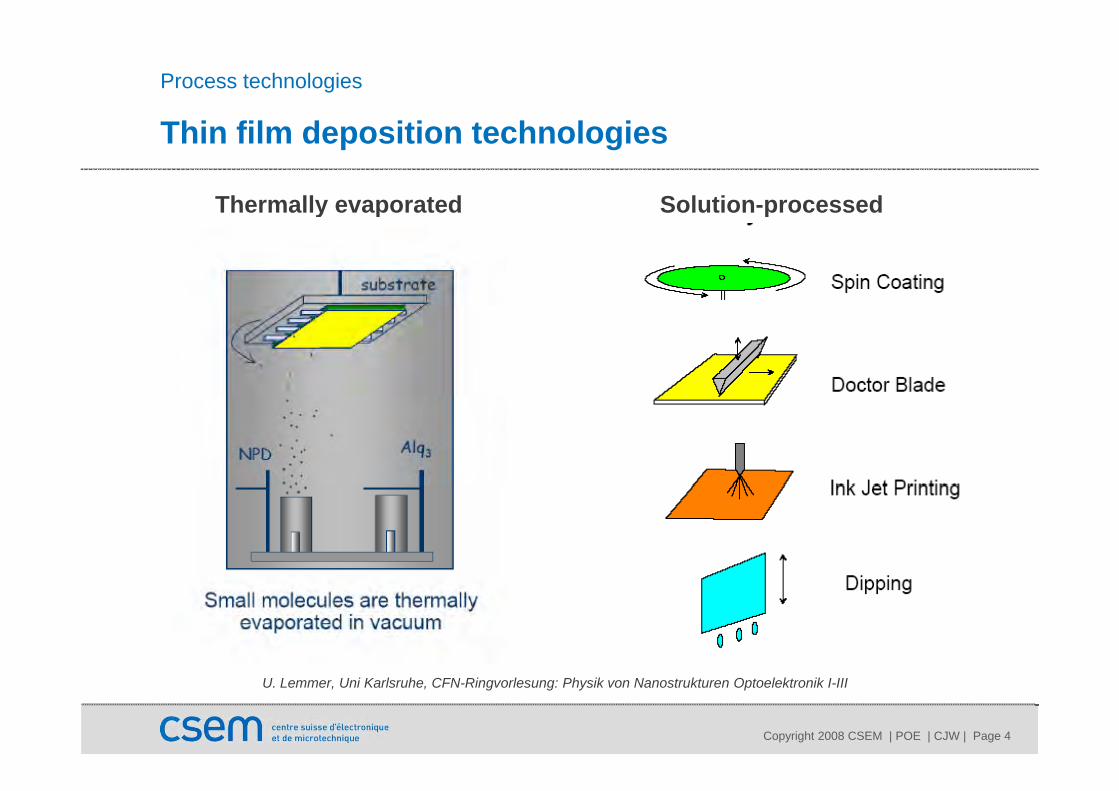
Process technologies
Thin film deposition technologies
Solution-processedThermally evaporated py p
Copyright 2008 CSEM | POE | CJW | Page 4
U. Lemmer, Uni Karlsruhe, CFN-Ringvorlesung: Physik von Nanostrukturen Optoelektronik I-III

O i O t l t i D i
Introduction
Organic Optoelectronic Devices
LED Photodiode Transistor
CathodeCathode A A A
Cathode
Organic Layer
urce
rain
Anode
Cathode
Glass substrate
Light Emitting PolymerCathode
V V
Glass substrateITO anodePolymer
Cathode
+ + + + + + + +
- - - - - - - - - - -Gate ElectrodeGate Insulator
Sour
Dra
Substrate
SONYSONY(2007)
DemonstratorsD P U i
Consumer Products
Kodak
PrototypesPhilips
Copyright 2008 CSEM | POE | CJW | Page 5
DuPont-Uniax

O i O t l t i
Introduction
Organic Optoelectronics
LED Photodiode Transistor
CathodeCathode A A A
Cathode
Organic Layer
urce
rain
Anode
Cathode
Glass substrate
Light Emitting PolymerCathode
V V
Glass substrateITO anodePolymer
Cathode
+ + + + + + + +
- - - - - - - - - - -Gate ElectrodeGate Insulator
Sour
Dra
Substrate
E l ti f EQE f i h t j tiEvolution of EQE for organic heterojunction photodiodes
60
70
80
0
10
20
30
40
50
EQE
(%)
Copyright 2008 CSEM | POE | CJW | Page 6
01992 1994 1996 1998 2000 2002 2004
Year

Li hti
Target Application: OLED lighting
Lighting
GE 04/2004
2010 2025
GE 04/2004
World Illumination Market [M$]
15000 30000Market [M$]
OLED-Illumination 1500 (10%) 15000 (50%)Illumination Market [M$]
1500 (10%) 15000 (50%)
Sources: DoE, BMBF
Copyright 2008 CSEM | POE | CJW | Page 7

R ll t R ll OLED f li hti li tiRoll-to-Roll OLEDs for lighting applications
• GE press release (~March 2008)
Copyright 2008 CSEM | POE | CJW | Page 8

Whit OLED til
Solution/Vacuum processed
White OLED tiles
Brigthness (cd/m2) 1000
Solution / (Vacuum) deposited
Luminous efficacy (lm/W)
> 25 (50, OLLA)
5000(spin-coated, by Siemens) Lifetime (h)
> 5000 (10000, OLLA)
Panel size (cm2) > 15×15Panel size (cm ) 15 15
Homogeneous large areas
Low cost
Copyright 2008 CSEM | POE | CJW | Page 9

Whit OLED til
Vacuum deposition
White OLED tiles (latest achivements)
UDCUDC
• phosphorescent OLED technology
102 lm/W• 102 lm/W
• CRI 70
NovaLED
• 35 lm/W
• CRI 90
t 100 000h @ b i ht f 1000 d/ 2• t 100,000h @ brightness of 1000 cd/m2.
Copyright 2008 CSEM | POE | CJW | Page 10
www.oled-info.com

H l t C t (NL)
PLED-signage on flexible substrate
Holst Centre (NL)
Copyright 2008 CSEM | POE | CJW | Page 11

Polymer Optoelectronics @ CSEM
Material & Device Optimization
Low-cost and / or Customizable Processes
Integrated Organic Optoelectronic Systems
LogoLEDTMPLED driven by organic IC
• Polymer LEDs
• Polymer Transistors
• Signage
• Illumination
• System Integration:
(oLEDs & oPDs & oFETs)
y g
• Polymer Transistors
• Polymer Photodiodes
• Illumination
• Plastic IC’s
(oLEDs & oPDs & oFETs)
• Development of additive printing processes
Copyright 2008 CSEM | POE | CJW | Page 12
p g p

St t f th A t P i & Ch t i ti
CSEM Capabilities
State-of-the-Art Processing & Characterization
• 150 m2 POE clean room environment50m2 Photolithography
Copyright 2008 CSEM | POE | CJW | Page 13
• 50m2 Photolithography

Integrated Organic Sensor System “SENSoLEDTM”Proximity SensorProximity Sensor
PLED PLED F8 (10 wt.%)
TFB (40 t %)
F8 (10 wt.%)
TFB (40 t %)
F8BT (40 wt %)
TFB (40 wt.%)
F8BT (40 wt %)
TFB (40 wt.%)
F8BT (40 wt.%) F8BT (40 wt.%)
1.0
0.08
0.10
rb. u
nits
)
ty (A
/W)
PLED i i
1.0
0.08
0.10
rb. u
nits
)
ty (A
/W)
PLED i i PPD PPD
0.50.04
0.06
nten
sity
(ar
Res
pons
ivit
3
PLED emission
PPD 0.50.04
0.06
nten
sity
(ar
Res
pons
ivit
3
PLED emission
PPD
P3HT (33 wt.%) PCBM (66 wt.%) P3HT (33 wt.%) PCBM (66 wt.%)
400 500 600 700 8000.00.00
0.02 P
LED
In
PPD
R 34% Overlap
400 500 600 700 8000.00.00
0.02 P
LED
In
PPD
R 34% Overlap
P. Schilinsky et al. Thin Solid Films, 451-452 105 (2004)
Copyright 2008 CSEM | POE | CJW | Page 14
400 500 600 700 800Wavelength (nm)
400 500 600 700 800Wavelength (nm)
451-452, 105 (2004).

SENSoLEDTMMonolithic Integration
SENSoLED
PPDs PPDs
PLED
ITO
PLED
ITO ITO
patterned Polyimide
ITO
patterned Polyimide
• Monolithically integrated• Monolithically integrated PLED & polymer PDs
• Position & Proximity sensory
• Touch screen
• Artificial haptic sense
Copyright 2008 CSEM | POE | CJW | Page 15
pL. Bürgi et al., Organic Electronics 7 (2006) 114
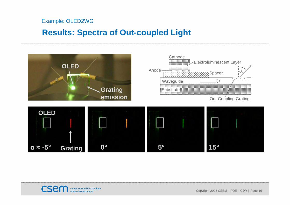
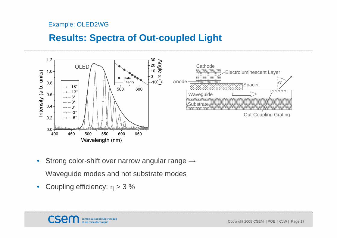
Results: Spectra of Out-coupled LightExample: OLED2WG
Results: Spectra of Out-coupled Light
C th d
OLEDSpacer
Electroluminescent Layer
Anode α
Cathode
Gratingemission
Substrate
Waveguide
Out-Coupling Grating
OLED
5° 15°α ≈ -5° 0°Grating 5 15α 5 0Grating
Copyright 2008 CSEM | POE | CJW | Page 16
Results: Spectra of Out-coupled LightExample: OLED2WG
Results: Spectra of Out-coupled Light
C th d
Spacer
Electroluminescent Layer
Anode α
Cathode
Substrate
Waveguide
Out-Coupling Grating
• Strong color-shift over narrow angular range →
Waveguide modes and not substrate modesWaveguide modes and not substrate modes
• Coupling efficiency: η > 3 %
Copyright 2008 CSEM | POE | CJW | Page 17

Future ApplicationsExample OLED2WG2OPD
Future Applications
C th dOG
• Point of Care DiagnosticsSpacer
Electroluminesc
Anode
Cathode
• Photonic Integrated Circuits Substrate
Waveguide
Out-Co
Λ1 Λ2 Λ3
INTEGRATED
FLUIDICS
INTEGRATED INTEGRATED SOURCE: OLED
INTEGRATED DETECTION: Spectrometer
SENSING LAYER
SUBSTRATE
Copyright 2008 CSEM | POE | CJW | Page 18

C l iConclusion
• Vacuum deposition multilayer structure high p y gperformance
• Applications
• Displays trend: white OLEDs & LCD (SID 2008)
• Illumination
• Solution processed solvent orthogonality simple structurestructure
• Applications
• Digital printing techniques custom designed• Digital printing techniques custom-designed signage, sensor systems, functional packaging
• The ultimate: Roll-to-Roll production
Copyright 2008 CSEM | POE | CJW | Page 19

A tAnnouncement
FSRM C “P l O t l t i T h l i d A li ti ”• FSRM Course “Polymer Optoelectronic Technologies and Applications”
• 29.09. 2008, CSEM Basel
www fsrm ch• www.fsrm.ch
• Electrosuisse Trilogie “Elektronik der Zukunft Organische Elektronik”• Electrosuisse Trilogie Elektronik der Zukunft, Organische Elektronik
• 25.06.2009, ZHAW Winterthur
• www electrosuisse ch• www.electrosuisse.ch
Copyright 2008 CSEM | POE | CJW | Page 20

Thank you for your attention!