±0.33°c accurate, 12-bit+ sign temperature sensor and ...2017-9-24 · lm92 snis110d – march...
TRANSCRIPT

LM92
www.ti.com SNIS110D –MARCH 2000–REVISED MARCH 2013
±0.33°C Accurate, 12-Bit + Sign Temperature Sensor and Thermal Window ComparatorWith Two-Wire Interface
Check for Samples: LM92
1FEATURES DESCRIPTIONThe LM92 is a digital temperature sensor and thermal
23• Window Comparison Simplifies Design ofwindow comparator with an I2C™ Serial Bus interfaceACPI-Compatible Temperature Monitoring andand an accuracy of ±0.33°C. The window-comparatorControlarchitecture of the LM92 eases the design of
• Serial Bus Interface temperature control systems. The open-drainInterrupt (INT) output becomes active whenever• Separate Open-Drain Outputs for Interrupt andtemperature goes outside a programmable window,Critical Temperature Shutdownwhile a separate Critical Temperature Alarm• Shutdown Mode to Minimize Power(T_CRIT_A) output becomes active when the
Consumption temperature exceeds a programmable critical limit.• Up to Four LM92s can be Connected to a The INT output can operate in either a comparator or
Single Bus event mode, while the T_CRIT_A output operates incomparator mode only.• 12-Bit + Sign OutputThe host can program both the upper and lower limits• Operation up to 150°Cof the window as well as the critical temperature limit.Programmable Hysteresis as well as a fault queueAPPLICATIONSare available to minimize false tripping. Two pins (A0,
• HVAC A1) are available for address selection. The sensor• Medical Electronics powers up with default thresholds of 2°C THYST, 10°C
TLOW, 64°C THIGH, and 80°C T_CRIT.• Electronic Test EquipmentThe LM92's 2.7V to 5.5V supply voltage range, Serial• System Thermal ManagementBus interface, 12-bit + sign output, and full-scale• Personal Computersrange of over 128°C make it ideal for a wide range of
• Office Electronics applications. These include thermal management and• Automotive protection applications in personal computers,
electronic test equipment, office electronics,automotive, medical and HVAC applications.KEY SPECIFICATIONS
• Supply Voltage 2.7V to 5.5V• Supply Current operating 350 μA (typ) 625 μA
(max) shutdown 5 μA (typ)• Temperature Accuracy
– 30°C, ±0.33°C (max)– 10°C to 50°C, ±0.50°C (max)– −10°C to 85°C, ±1.0°C (max)– 125°C, ±1.25°C (max)– −25°C to 150°C, ±1.5°C (max)
• Linearity ±0.5°C (max)• Resolution 0.0625°C
1
Please be aware that an important notice concerning availability, standard warranty, and use in critical applications ofTexas Instruments semiconductor products and disclaimers thereto appears at the end of this data sheet.
2I2C is a trademark of dcl_owner.3All other trademarks are the property of their respective owners.
PRODUCTION DATA information is current as of publication date. Copyright © 2000–2013, Texas Instruments IncorporatedProducts conform to specifications per the terms of the TexasInstruments standard warranty. Production processing does notnecessarily include testing of all parameters.

LM92
SNIS110D –MARCH 2000–REVISED MARCH 2013 www.ti.com
Simplified Block Diagram
Connection Diagram
SOICSee Package Number D (R-PDSO-G8)
Pin DescriptionLabel Pin No. Function Typical Connection
SDA 1 Serial Bi-Directional Data Line. Open Drain Output From Controller
SCL 2 Serial Bus Clock Input From Controller
T_CRIT_A 3 Critical Temperature Alarm Open Drain Output Pull Up Resistor, Controller Interrupt Line or SystemHardware Shutdown
GND 4 Power Supply Ground Ground
INT 5 Interrupt Open Drain Output Pull Up Resistor, Controller Interrupt Line
+V S 8 Positive Supply Voltage Input DC Voltage from 2.7V to 5.5V
A0–A1 7,6 User-Set Address Inputs Ground (Low, “0”) or +VS (High, “1”)
2 Submit Documentation Feedback Copyright © 2000–2013, Texas Instruments Incorporated
Product Folder Links: LM92

LM92
www.ti.com SNIS110D –MARCH 2000–REVISED MARCH 2013
Typical Application
Figure 1.
These devices have limited built-in ESD protection. The leads should be shorted together or the device placed in conductive foamduring storage or handling to prevent electrostatic damage to the MOS gates.
Absolute Maximum Ratings (1)
Supply Voltage −0.3 V to 6.5V
Voltage at any Pin −0.3 V to (+VS + 0.3V)
Input Current at any Pin 5 mA
Package Input Current (2) 20 mA
T_CRIT_A and INT Output Sink Current 10 mA
T_CRIT_A and INT Output Voltage 6.5V
Storage Temperature −65°C to +125°C
ESD Susceptibility (3) Human Body Model 2500V
Machine Model 250V
Soldering process must comply with Reflow Temperature Profile specifications. Refer to http://www.ti.com/lit/SNOA549. (4)
(1) Absolute Maximum Ratings indicate limits beyond which damage to the device may occur. DC and AC electrical specifications do notapply when operating the device beyond its rated operating conditions.
(2) When the input voltage (VI) at any pin exceeds the power supplies (VI < GND or VI > +VS) the current at that pin should be limited to 5mA. The 20 mA maximum package input current rating limits the number of pins that can safely exceed the power supplies with an inputcurrent of 5 mA to four.
(3) Human body model, 100 pF discharged through a 1.5 kΩ resistor. Machine model, 200 pF discharged directly into each pin.(4) Reflow temperature profiles are different for lead-free and non-lead-free packages.
Operating Ratings (1) (2)
Specified Temperature Range (3), TMIN to TMAX −55°C to +150°C
Supply Voltage Range (+VS) +2.7V to +5.5V
(1) Absolute Maximum Ratings indicate limits beyond which damage to the device may occur. DC and AC electrical specifications do notapply when operating the device beyond its rated operating conditions.
(2) LM92 θJA (thermal resistance, junction-to-ambient) when attached to a printed circuit board with 2 oz. foil is 200 °C/W.(3) While the LM92 has a full-scale-range in excess of 128°C, prolonged operation at temperatures above 125 °C is not recommended.
Copyright © 2000–2013, Texas Instruments Incorporated Submit Documentation Feedback 3
Product Folder Links: LM92

LM92
SNIS110D –MARCH 2000–REVISED MARCH 2013 www.ti.com
Electrical Characteristics Temperature-to-Digital Converter CharacteristicsUnless otherwise noted, these specifications apply for +VS= +2.7V to +5.5V for LM92CIM . Boldface limits apply for TA = TJ
= TMIN to TMAX; all other limits TA= TJ= +25°C, unless otherwise noted.
Typical (1) Limits (2) UnitParameter Conditions (Limit)
Accuracy (This is a summary. For more T A = +30°C, +VS = 3.3V to 4.0V ±0.33detailed information please see (3)) T A = 10°C or +50°C, +VS = 3.3V to ±0.50
4.0V
T A = −10 °C or +85°C, +VS = 3.3V ±1.00 °C (max)to 4.0V
T A = +125°C, +VS = 4.0V ±1.25
T A = −25°C to 150°C, +VS = 4.0V ±1.50
Resolution (4) 13 Bits0.0625 °C
Linearity (5) ±0.5 °C (max)
Offset Error of Transfer Function (6) +VS = 4.0V °C (max)
Offset Error of Transfer Function Supply 2.7V ≤ +VS< 3.6V °C/V (max)Sensitivity 3.6V ≤ +VS≤ 5.5V °C/V (max)
Temperature Conversion Time (7) 500 1000 ms
Quiescent Current I2C Inactive 0.35 mA
I2C Active 0.35 0.625 mA (max)
Shutdown Mode 5 µA
T HYST Default Temperature (8) (9)2 °C
T LOW Default Temperature (9) 10 °C
T HIGH Default Temperature (9) 64 °C
T C Default Temperature (9) 80 °C
(1) Typical values are at TA = 25 °C and represent most likely parametric norm.(2) Limits are guaranteed to TI's AOQL (Average Outgoing Quality Level).(3) The limits found in Table 1 supersede the limits shown in the Electrical Characteristics Table. The Accuracy specification includes errors
due to linearity, offset and gain. The accuracy specification includes effects of self heating with negligible digital output loading. Pull-upresistors should be maximized (10k typical recommended), so that self heating due to digital output loading is negligible.
(4) Limits at intermediate temperatures can be calculated using a straight line interpolation as shown in Figure 2 and Figure 3.(5) Linearity Error is defined as the worse case difference of an actual reading to that of a calculated reading derived from the straight line
whose endpoints are measured at 30°C and 125°C for the range of 30°C to 125°C or whose endpoints are measured at 30°C and−25°C for the range of 30°C to −25°.
(6) Offset Error calibration should be done at 30°C. The residual error of the transfer function is then equivalent to the Accuracy Limit minusthe Offset Limit. This does not take into account the power supply sensitivity of the offset error. Nor, does it take into account the errorintroduced by the calibration system used.
(7) This specification is provided only to indicate how often temperature data is updated. The LM92 can be read at any time without regardto conversion state (and will yield last conversion result). If a conversion is in process it will be interrupted and restarted after the end ofthe read.
(8) 12 bits + sign, two's complement(9) Default values set at power up.
Figure 2. Accuracy vs Temperature with +Vs = 5V
4 Submit Documentation Feedback Copyright © 2000–2013, Texas Instruments Incorporated
Product Folder Links: LM92

LM92
www.ti.com SNIS110D –MARCH 2000–REVISED MARCH 2013
Figure 3. Accuracy vs Temperature with +Vs = 3.3V
Table 1. Temperature Accuracy Parameter Limits
Conditions +VS=2.7V +VS=3.3V +VS=4V +VS=5V +VS=5.5V Unit
T A = −25°C −1.35/+1.50 −1.25/+1.50 −1.25/+1.50 −1.05/+1.70 −1.05/+1.80 °C (max)
T A = −10°C ±1.00 −0.90/+1.00 −0.90/+1.00 −0.70/+1.20 −0.70/+1.30 °C (max)
T A = 0°C −0.80/+0.75 −0.70/+0.75 −0.70/+0.75 −0.50/+0.95 −0.50/+1.05 °C (max)
T A = 10°C −0.60/+0.50 ±0.50 ±0.50 −0.30/+0.70 −0.30/+0.80 °C (max)
T A = 30°C −0.43/+0.33 ±0.33 ±0.33 −0.13/+0.53 −0.13/+0.63 °C (max)
T A = 50°C −0.60/+0.50 ±0.50 ±0.50 −0.30/+0.70 −0.30/+0.80 °C (max)
T A = 85°C −1.10/+0.85 −1.00/+0.85 −1.00/+0.85 −0.80/+1.05 −0.80/+1.15 °C (max)
T A = 125°C −1.60/+1.25 −1.50/+1.25 ±1.25 −1.05/+1.45 −1.05/+1.55 °C (max)
T A = 150°C ±1.90 −1.75/+1.50 ±1.50 −1.30/+1.70 −1.30/+1.80 °C (max)
Digital DC CharacteristicsUnless otherwise noted, these specifications apply for +VS= +2.7V to +5.5V for LM92CIM . Boldface limits apply for TA = TJ
= TMIN to TMAX; all other limits TA= TJ= +25 °C, unless otherwise noted.
Typical (1) Limits (2) UnitSymbol Parameter Conditions (Limit)
V IN(1) SDA and SCL Logical “1” Input +VS × 0.7 V (min)Voltage
+VS+0.3 V (max)
V IN(0) SDA and SCL Logical “0” Input −0.3 V (min)Voltage
+VS × 0.3 V (max)
VIN(HYST) SDA and SCL Digital Input Hysteresis 500 250 mV (min)
V IN(1) A0 and A1 Logical “1” Input Voltage 2.0 V (min)
+VS+0.3 V (max)
V IN(0) A0 and A1 Logical “0” Input Voltage −0.3 V (min)
0.7 V (max)
I IN(1) Logical “1” Input Current V IN = + VS 0.005 1.0 µA (max)
I IN(0) Logical “0” Input Current V IN = 0 V −0.005 −1.0 µA (max)
C IN Capacitance of All Digital Inputs 20 pF
I OH High Level Output Current V OH = + VS 10 µA (max)
V OL Low Level Output Voltage I OL = 3 mA 0.4 V (max)
(1) Typical values are at TA = 25 °C and represent most likely parametric norm.(2) Limits are guaranteed to TI's AOQL (Average Outgoing Quality Level).
Copyright © 2000–2013, Texas Instruments Incorporated Submit Documentation Feedback 5
Product Folder Links: LM92

LM92
SNIS110D –MARCH 2000–REVISED MARCH 2013 www.ti.com
Digital DC Characteristics (continued)Unless otherwise noted, these specifications apply for +VS= +2.7V to +5.5V for LM92CIM . Boldface limits apply for TA = TJ
= TMIN to TMAX; all other limits TA= TJ= +25 °C, unless otherwise noted.
Typical (1) Limits (2) UnitSymbol Parameter Conditions (Limit)
T_CRIT_A Output Saturation Voltage I OUT = 4.0 mA 0.8 V (max)(3)
T_CRIT_A Delay 1 Conversions(max)
t OF Output Fall Time C L = 400 pF 250 ns (max)
I O = 3 mA
(3) For best accuracy, minimize output loading. 10k pull-ups resistors should be sufficient. Higher sink currents can affect sensor accuracywith internal heating. This can cause an error of 0.64 °C at full rated sink current and saturation voltage based on junction-to-ambientthermal resistance.
Serial Bus Digital Switching CharacteristicsUnless otherwise noted, these specifications apply for +VS= +2.7V to +5.5V for LM92CIM . Boldface limits apply for TA = TJ
= TMIN to TMAX; all other limits TA= TJ= +25 °C, unless otherwise noted. CL (load capacitance) on output lines = 80 pF unlessotherwise specified. Boldface limits apply for TA = TJ = TMIN to TMAX; all other limits TA = TJ = +25 °C, unless otherwise noted.
Typical (1) Limits (2) (3) UnitSymbol Parameter Conditions (Limit)
t 1 SCL (Clock) Period 2.5 µs(min)
1 ms(max)
t 2 Data in Set-Up Time to SCL High 100 ns(min)
t 3 Data Out Stable after SCL Low 0 ns(min)
t 4 SDA Low Set-Up Time to SCL Low (Start Condition) 100 ns(min)
t 5 SDA High Hold Time after SCL High (Stop Condition) 100 ns(min)
tTIMEOUT SDA and SCL Time Low for Reset of Serial Interface (4) 75 ms (min)300 ms (max)
(1) Typical values are at TA = 25 °C and represent most likely parametric norm.(2) Limits are guaranteed to TI's AOQL (Average Outgoing Quality Level).(3) Timing specifications are tested at the bus input logic levels (Vin(0)=0.3xVA for a falling edge and Vin(1)=0.7xVA for a rising edge) when
the SCL and SDA edge rates are similar.(4) Holding the SDA and/or SCL lines Low for a time interval greater than tTIMEOUT will cause the LM92 to reset SCL and SDA to the IDLE
state of the serial bus communication (SDA and SCL set High).
Figure 4. Serial Bus Communication
6 Submit Documentation Feedback Copyright © 2000–2013, Texas Instruments Incorporated
Product Folder Links: LM92

LM92
www.ti.com SNIS110D –MARCH 2000–REVISED MARCH 2013
Figure 5. Temperature-to-Digital Transfer Function (Non-linear scale for clarity)
Copyright © 2000–2013, Texas Instruments Incorporated Submit Documentation Feedback 7
Product Folder Links: LM92

LM92
SNIS110D –MARCH 2000–REVISED MARCH 2013 www.ti.com
FUNCTIONAL DESCRIPTION
The LM92 temperature sensor incorporates a band-gap type temperature sensor, 13-bit ADC, and a digitalcomparator with user-programmable upper and lower limit values. The comparator activates either the INT linefor temperatures outside the TLOW and THIGH window, or the T_CRIT_A line for temperatures which exceedT_CRIT. The lines are programmable for mode and polarity.
TEMPERATURE COMPARISON
LM92 provides a window comparison against a lower (TLOW) and upper (THIGH) trip point. A second upper trippoint (T_CRIT) functions as a critical alarm shutdown. Figure 7 depicts the comparison function as well as themodes of operation.
Status Bits
The internal Status bits operate as follows:
“True”: Temperature above a THIGH or T_CRIT is “true” for those respective bits. A “true” for TLOW istemperature below TLOW.
“False”: Assuming temperature has previously crossed above THIGH or T_CRIT, then the temperature mustdrop below the points corresponding THYST (THIGH − THYST or T_CRIT − THYST) in order for the condition to befalse. For TLOW, assuming temperature has previously crossed below TLOW, a “false” occurs when temperaturegoes above TLOW + THYST.
The Status bits are not affected by reads or any other actions, and always represent the state of temperature vs.setpoints.
Hardwire Outputs
The T_CRIT_A hardwire output mirrors the T_CRIT_A flag, when the flag is true, the T_CRIT_A output isasserted at all times regardless of mode. Reading the LM92 has no effect on the T_CRIT_A output, although theinternal conversion is restarted.
The behavior of the INT hardwire output is as follows:
Comparator Interrupt Mode (Default): User reading part resets output until next measurement completes. Ifcondition is still true, output is set again at end of next conversion cycle. For example, if a user never reads thepart, and temperature goes below TLOW then INT becomes active. It would stay that way until temperature goesabove TLOW + THYST. However if the user reads the part, the output would be reset. At the end of the nextconversion cycle, if the condition is true, it is set again. If not, it remains reset.
Event Interrupt Mode: User reading part resets output until next condition "event" occurs (in other words,output is only set once for a true condition, if reset by a read, it remains reset until the next triggering thresholdhas been crossed). Conversely, if a user never read the part, the output would stay set indefinitely after the firstevent that set the output. An “event” for Event Interrupt Mode is defined as:1. Transitioning upward across a setpoint, or2. Transitioning downward across a setpoint's corresponding hysteresis (after having exceeded that setpoint).
For example, if a user never read the part, and temperature went below TLOW then INT would become active. Itwould stay that way forever if a user never read the part.
However if the user read the part, the output would be reset. Even if the condition is true, it will remain reset. Thetemperature must cross above TLOW + THYST to set the output again.
In either mode, reading any register in the LM92 restarts the conversion. This allows a designer to know exactlywhen the LM92 begins a comparison. This prevents unnecessary Interrupts just after reprogramming setpoints.Typically, system Interrupt inputs are masked prior to reprogramming trip points. By doing a read just afterresetting trip points, but prior to unmasking, unexpected Interrupts are prevented.
Avoid programming setpoints so close that their hysteresis values overlap. An example would be that with aTHYST value of 2 °C then setting THIGH and TLOW to within 4 °C of each other will violate this restriction. To bemore specific, with THYST set to 2 °C assume THIGH set to 64 °C. If TLOW is set equal to, or higher than 60 °C thisrestriction is violated.
8 Submit Documentation Feedback Copyright © 2000–2013, Texas Instruments Incorporated
Product Folder Links: LM92

LM92
www.ti.com SNIS110D –MARCH 2000–REVISED MARCH 2013
DEFAULT SETTINGS
The LM92 always powers up in a known state. LM92 power up default conditions are:1. Comparator Interrupt Mode2. TLOW set to 10 °C3. THIGH set to 64 °C4. T_CRIT set to 80 °C5. THYST set to 2 °C6. INT and T_CRIT_A active low7. Pointer set to “00”; Temperature Register
The LM92 registers will always reset to these default values when the power supply voltage is brought up fromzero volts as the supply crosses the voltage level plotted in the following curve. The LM92 registers will resetagain when the power supply drops below the voltage plotted in this curve.
Figure 6. Average Power on Reset Voltage vs Temperature
SERIAL BUS INTERFACE
The LM92 operates as a slave on the Serial Bus, so the SCL line is an input (no clock is generated by the LM92)and the SDA line is a bi-directional serial data line. According to Serial Bus specifications, the LM92 has a 7-bitslave address. The five most significant bits of the slave address are hard wired inside the LM92 and are“10010”. The two least significant bits of the address are assigned to pins A1–A0, and are set by connectingthese pins to ground for a low, (0); or to +VS for a high, (1).
Therefore, the complete slave address is:
1 0 0 1 0 A1 A0
MSB LSB
Copyright © 2000–2013, Texas Instruments Incorporated Submit Documentation Feedback 9
Product Folder Links: LM92

LM92
SNIS110D –MARCH 2000–REVISED MARCH 2013 www.ti.com
Note: Event Interrupt mode is drawn as if the user is reading the part. If the user doesn't read, the outputs would golow and stay that way until the LM92 is read. Comparator Interrupt Mode is drawn as if the user never reads the part.If the user does read, the outputs will go high once read instruction is executed and, if the fault condition still exists,go low at the end of the next conversion.
Figure 7. Temperature Response Diagram
TEMPERATURE DATA FORMAT
Temperature data can be read from the Temperature and Set Point registers; and written to the Set Pointregisters. Temperature data can be read at any time, although reading faster than the conversion time of theLM92 will prevent data from being updated. Temperature data is represented by a 13-bit, two's complement wordwith an LSB (Least Significant Bit) equal to 0.0625 °C:
Table 2. Temperature Data Output
Temperature Digital Output
Binary Hex
+130°C 0 1000 0 010 0000 08 20h
+125 °C 0 0111 1101 0000 07 D0h
+80 °C 0 0101 0000 0000 05 00h
+64 °C 0 0100 0000 0000 04 00h
+25 °C 0 0001 1001 0000 01 90h
+10 °C 0 0000 1010 0000 00 A0h
+2 °C 0 0000 0010 0000 00 20h
10 Submit Documentation Feedback Copyright © 2000–2013, Texas Instruments Incorporated
Product Folder Links: LM92

LM92
www.ti.com SNIS110D –MARCH 2000–REVISED MARCH 2013
Table 2. Temperature Data Output (continued)
Temperature Digital Output
Binary Hex
+0.0625 °C 0 0000 0000 0001 00 01h
0 °C 00 0000 0000 00 00h
−0.0625 °C 1 1111 1111 1111 1F FFh
−25 °C 1 1110 0111 0000 1E 70h
−55 °C 1 1100 1001 0000 1C 90h
SHUTDOWN MODE
Shutdown mode is enabled by setting the shutdown bit in the Configuration register via the Serial Bus. Shutdownmode reduces power supply current to 5 µA typical. T_CRIT_A is reset if previously set. Since conversions arestopped during shutdown, T_CRIT_A and INT will not be operational. The Serial Bus interface remains active.Activity on the clock and data lines of the Serial Bus may slightly increase shutdown mode quiescent current.Registers can be read from and written to in shutdown mode. The LM92 takes milliseconds to respond to theshutdown command.
INT AND T_CRIT_A OUTPUT
The INT and T_CRIT_A outputs are open-drain outputs and do not have internal pull-ups. A "high" level will notbe observed on these pins until pull-up current is provided from some external source, typically a pull-up resistor.Choice of resistor value depends on many system factors but, in general, the pull-up resistor should be as largeas possible. This will minimize any errors due to internal heating of the LM92. The maximum resistance of thepull up, based on LM92 specification for High Level Output Current, to provide a 2 volt high level, is 30K ohms.
FAULT QUEUE
A fault queue of 4 faults is provided to prevent false tripping when the LM92 is used in noisy environments. The 4faults must occur consecutively to set flags as well as INT and T_CRIT_A outputs. The fault queue is enabled bysetting bit 4 of the Configuration Register high (see CONFIGURATION REGISTER ).
Copyright © 2000–2013, Texas Instruments Incorporated Submit Documentation Feedback 11
Product Folder Links: LM92

LM92
SNIS110D –MARCH 2000–REVISED MARCH 2013 www.ti.com
INTERNAL REGISTER STRUCTURE
Figure 8.
There are four data registers in the LM92, selected by the Pointer register. At power-up the Pointer is set to “00”;the location for the Temperature Register. The Pointer register latches the last location it was set to. In InterruptMode, a read from the LM92 resets the INT output. Placing the device in Shutdown mode resets the INT andT_CRIT_A outputs. All registers are read and write, except the Temperature register which is read only.
A write to the LM92 will always include the address byte and the Pointer byte. A write to the Configurationregister requires one data byte, while the TLOW, THIGH, and T_CRIT registers require two data bytes.
Reading the LM92 can take place either of two ways: If the location latched in the Pointer is correct (most of thetime it is expected that the Pointer will point to the Temperature register because it will be the data mostfrequently read from the LM92), then the read can simply consist of an address byte, followed by retrieving thecorresponding number of data bytes. If the Pointer needs to be set, then an address byte, pointer byte, repeatstart, and another address byte plus required number of data bytes will accomplish a read.
The first data byte is the most significant byte with most significant bit first, permitting only as much data asnecessary to be read to determine the temperature condition. For instance, if the first four bits of the temperaturedata indicates a critical condition, the host processor could immediately take action to remedy the excessivetemperature. At the end of a read, the LM92 can accept either Acknowledge or No Acknowledge from the Master(No Acknowledge is typically used as a signal for the slave that the Master has read its last byte).
An inadvertent 8-bit read from a 16-bit register, with the D7 bit low, can cause the LM92 to stop in a state wherethe SDA line is held low as shown in Figure 9. This can prevent any further bus communication until at least 9additional clock cycles have occurred. Alternatively, the master can issue clock cycles until SDA goes high, atwhich time issuing a “Stop” condition will reset the LM92.
12 Submit Documentation Feedback Copyright © 2000–2013, Texas Instruments Incorporated
Product Folder Links: LM92

LM92
www.ti.com SNIS110D –MARCH 2000–REVISED MARCH 2013
Figure 9. Inadvertent 8-Bit Read from 16-Bit Register where D7 is Zero (“0”)
POINTER REGISTER
(Selects which registers will be read from or written to):
P7 P6 P5 P4 P3 P2 P1 P0
0 0 0 0 0 Register Select
P0–P2: Register Select:
P2 P1 P0 Register
0 0 0 Temperature (Read only) (Power-up default)
0 0 1 Configuration (Read/Write)
0 1 0 THYST (Read/Write)
0 1 1 T_CRIT (Read/Write)
1 0 0 TLOW (Read/Write)
1 0 1 THIGH (Read/Write)
1 1 1 Manufacturer's ID
P3–P7: Must be kept zero.
TEMPERATURE REGISTER
Table 3. (Read Only):
D15 D14 D13 D12 D11 D10 D9 D8 D7 D6 D5 D4 D3 D2 D1 D0
Sign MSB Bit 10 Bit 9 Bit 8 Bit 7 Bit 6 Bit 5 Bit 4 Bit 3 Bit 2 Bit 1 Bit 0 CRIT HIGH LOW
Status Bits
D0–D2: Status Bits
D3–D15: Temperature Data. One LSB = 0.0625°C. Two's complement format.
CONFIGURATION REGISTER
Table 4. (Read/Write):
D7 D6 D5 D4 D3 D2 D1 D0
0 0 0 Fault Queue INT Polarity T_CRIT_A INT Mode ShutdownPolarity
D0: Shutdown - When set to 1 the LM92 goes to low power shutdown mode. Power up default of “0”.
D1: Interrupt mode - 0 is Comparator Interrupt mode, 1 is Event Interrupt mode. Power up default of “0”.
D2, D3: T_CRIT_A and INT Polarity - 0 is active low, 1 is active high. Outputs are open-drain. Power up defaultof “0”
D4: Fault Queue - When set to 1 the Fault Queue is enabled, see FAULT QUEUE. Power up default of “0”.
D5–D7: These bits are used for production testing and must be kept zero for normal operation.
Copyright © 2000–2013, Texas Instruments Incorporated Submit Documentation Feedback 13
Product Folder Links: LM92
LM92
SNIS110D –MARCH 2000–REVISED MARCH 2013 www.ti.com
THYST, TLOW, THIGH AND T_CRIT_A REGISTERS
Table 5. (Read/Write):
D15 D14 D13 D12 D11 D10 D9 D8 D7 D6 D5 D4 D3 D2 D1 D0
Sign MSB Bit 10 Bit 9 Bit 8 Bit7 Bit6 Bit5 Bit 4 Bit 3 Bit 2 Bit 1 Bit 0 X X X
D0–D2: Undefined
D3–D15: THYST, TLOW, THIGH or T_CRIT Trip Temperature Data. Power up default is TLOW = 10°C, THIGH = 64°C,T_CRIT = 80°C, THYST = 2°C.
THYST is subtracted from THIGH, and T_CRIT, and added to TLOW.
Avoid programming setpoints so close that their hysteresis values overlap. See TEMPERATURE COMPARISON.
Manufacturer's Identification Register
Table 6. (Read only):
D15 D14 D13 D12 D11 D10 D9 D8 D7 D6 D5 D4 D3 D2 D1 D0
1 0 0 0 0 0 0 0 0 0 0 0 0 0 0 1
D0–D15: Manufactures ID.
14 Submit Documentation Feedback Copyright © 2000–2013, Texas Instruments Incorporated
Product Folder Links: LM92

LM92
www.ti.com SNIS110D –MARCH 2000–REVISED MARCH 2013
I2C TIMING DIAGRAMS
Figure 10. Typical 2-Byte Read From Preset Pointer Location Such as Temp or Comparison Registers
Figure 11. Typical Pointer Set Followed by Immediate Read for 2-Byte Register such as Temp orComparison Registers
Figure 12. Typical 1-Byte Read from Configuration Register with Preset Pointer
Figure 13. Typical Pointer Set Followed by Immediate Read from Configuration Register
Figure 14. Configuration Register Write
Figure 15. Comparison Register Write
Copyright © 2000–2013, Texas Instruments Incorporated Submit Documentation Feedback 15
Product Folder Links: LM92

LM92
SNIS110D –MARCH 2000–REVISED MARCH 2013 www.ti.com
APPLICATION HINTS
The temperature response graph in Figure 16 depicts a typical application designed to meet ACPI requirements.In this type of application, the temperature scale is given an arbitrary value of "granularity", or the window withinwhich temperature notification events should occur. The LM92 can be programmed to the window size chosen bythe designer, and will issue interrupts to the processor whenever the window limits have been crossed. Theinternal flags permit quick determination of whether the temperature is rising or falling.
The T_CRIT limit would typically use its separate output to activate hardware shutdown circuitry separate fromthe processor. This is done because it is expected that if temperature has gotten this high that the processor maynot be responding. The separate circuitry can then shut down the system, usually by shutting down the powersupply.
Note that the INT and T_CRIT_A outputs are separate, but can be wire-ORed together. Alternatively theT_CRIT_A can be diode ORed to the INT line in such a way that a T_CRIT_A event activates the INT line, but anINT event does not activate the T_CRIT_A line. This may be useful in the event that it is desirable to notify boththe processor and separate T_CRIT_A shutdown circuitry of a critical temperature alarm at the same time(maybe the processor is still working and can coordinate a graceful shutdown with the separate shutdowncircuit).
To implement ACPI compatible sensing it is necessary to sense whenever the temperature goes outside thewindow, issue an interrupt, service the interrupt, and reprogram the window according to the desired granularityof the temperature scale. The reprogrammed window will now have the current temperature inside it, ready toissue an interrupt whenever the temperature deviates from the current window.
To understand this graph, assume that at the left hand side the system is at some nominal temperature. For the1st event temperature rises above the upper window limit, THIGH, causing INT to go active. The system respondsto the interrupt by querying the LM92's status bits and determines that THIGH was exceeded, indicating thattemperature is rising. The system then programs the temperature limits to a value higher by an amount equal tothe desired granularity. Note that in Event Interrupt Mode, reprogramming the limits has caused a second,known, interrupt to be issued since temperature has been returned within the window. In Comparator InterruptMode, the LM92 simply stops issuing interrupts.
The 2nd event is another identical rise in temperature. The 3rd event is typical of a drop in temperature. This isone of the conditions that demonstrates the power of the LM92, as the user receives notification that a lower limitis exceeded in such a way that temperature is dropping.
The Critical Alarm Event activates the separate T_CRIT_A output. Typically, this would feed circuitry separatefrom the processor on the assumption that if the system reached this temperature, the processor might not beresponding.
16 Submit Documentation Feedback Copyright © 2000–2013, Texas Instruments Incorporated
Product Folder Links: LM92

LM92
www.ti.com SNIS110D –MARCH 2000–REVISED MARCH 2013
Note: Event Interrupt mode is drawn as if the user is reading the part. If the user doesn't read, the outputs would golow and stay that way until the LM92 is read.
Figure 16. Temperature Response Diagram for ACPI Implementation
Typical Applications
Figure 17. Typical Application
Copyright © 2000–2013, Texas Instruments Incorporated Submit Documentation Feedback 17
Product Folder Links: LM92

LM92
SNIS110D –MARCH 2000–REVISED MARCH 2013 www.ti.com
Figure 18. Remote HVAC temperature sensor communicates via 3 wires, including thermostat signals
Figure 19. ACPI Compatible Terminal Alarm Shutdown
By powering the LM92 from auxiliary output of the power supply, a non-functioning overheated computer can bepowered down to preserve as much of the system as possible.
18 Submit Documentation Feedback Copyright © 2000–2013, Texas Instruments Incorporated
Product Folder Links: LM92

LM92
www.ti.com SNIS110D –MARCH 2000–REVISED MARCH 2013
REVISION HISTORY
Changes from Revision C (March 2013) to Revision D Page
• Changed layout of National Data Sheet to TI format .......................................................................................................... 18
Copyright © 2000–2013, Texas Instruments Incorporated Submit Documentation Feedback 19
Product Folder Links: LM92

PACKAGE OPTION ADDENDUM
www.ti.com 23-Sep-2017
Addendum-Page 1
PACKAGING INFORMATION
Orderable Device Status(1)
Package Type PackageDrawing
Pins PackageQty
Eco Plan(2)
Lead/Ball Finish(6)
MSL Peak Temp(3)
Op Temp (°C) Device Marking(4/5)
Samples
LM92CIM NRND SOIC D 8 95 TBD Call TI Call TI -55 to 150 LM92CIM
LM92CIM/NOPB ACTIVE SOIC D 8 95 Green (RoHS& no Sb/Br)
CU SN Level-1-260C-UNLIM -55 to 150 LM92CIM
LM92CIMX/NOPB ACTIVE SOIC D 8 2500 Green (RoHS& no Sb/Br)
CU SN Level-1-260C-UNLIM -55 to 150 LM92CIM
(1) The marketing status values are defined as follows:ACTIVE: Product device recommended for new designs.LIFEBUY: TI has announced that the device will be discontinued, and a lifetime-buy period is in effect.NRND: Not recommended for new designs. Device is in production to support existing customers, but TI does not recommend using this part in a new design.PREVIEW: Device has been announced but is not in production. Samples may or may not be available.OBSOLETE: TI has discontinued the production of the device.
(2) RoHS: TI defines "RoHS" to mean semiconductor products that are compliant with the current EU RoHS requirements for all 10 RoHS substances, including the requirement that RoHS substancedo not exceed 0.1% by weight in homogeneous materials. Where designed to be soldered at high temperatures, "RoHS" products are suitable for use in specified lead-free processes. TI mayreference these types of products as "Pb-Free".RoHS Exempt: TI defines "RoHS Exempt" to mean products that contain lead but are compliant with EU RoHS pursuant to a specific EU RoHS exemption.Green: TI defines "Green" to mean the content of Chlorine (Cl) and Bromine (Br) based flame retardants meet JS709B low halogen requirements of <=1000ppm threshold. Antimony trioxide basedflame retardants must also meet the <=1000ppm threshold requirement.
(3) MSL, Peak Temp. - The Moisture Sensitivity Level rating according to the JEDEC industry standard classifications, and peak solder temperature.
(4) There may be additional marking, which relates to the logo, the lot trace code information, or the environmental category on the device.
(5) Multiple Device Markings will be inside parentheses. Only one Device Marking contained in parentheses and separated by a "~" will appear on a device. If a line is indented then it is a continuationof the previous line and the two combined represent the entire Device Marking for that device.
(6) Lead/Ball Finish - Orderable Devices may have multiple material finish options. Finish options are separated by a vertical ruled line. Lead/Ball Finish values may wrap to two lines if the finishvalue exceeds the maximum column width.
Important Information and Disclaimer:The information provided on this page represents TI's knowledge and belief as of the date that it is provided. TI bases its knowledge and belief on informationprovided by third parties, and makes no representation or warranty as to the accuracy of such information. Efforts are underway to better integrate information from third parties. TI has taken andcontinues to take reasonable steps to provide representative and accurate information but may not have conducted destructive testing or chemical analysis on incoming materials and chemicals.TI and TI suppliers consider certain information to be proprietary, and thus CAS numbers and other limited information may not be available for release.

PACKAGE OPTION ADDENDUM
www.ti.com 23-Sep-2017
Addendum-Page 2
In no event shall TI's liability arising out of such information exceed the total purchase price of the TI part(s) at issue in this document sold by TI to Customer on an annual basis.

TAPE AND REEL INFORMATION
*All dimensions are nominal
Device PackageType
PackageDrawing
Pins SPQ ReelDiameter
(mm)
ReelWidth
W1 (mm)
A0(mm)
B0(mm)
K0(mm)
P1(mm)
W(mm)
Pin1Quadrant
LM92CIMX/NOPB SOIC D 8 2500 330.0 12.4 6.5 5.4 2.0 8.0 12.0 Q1
PACKAGE MATERIALS INFORMATION
www.ti.com 24-Aug-2017
Pack Materials-Page 1
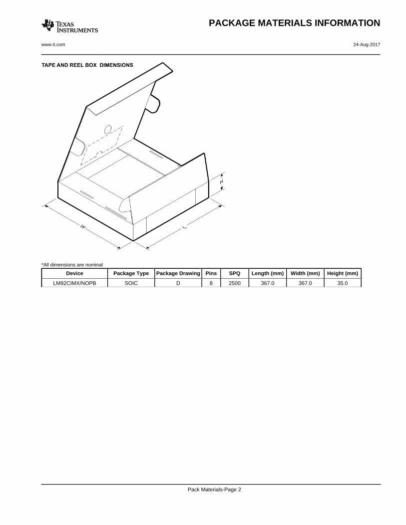
*All dimensions are nominal
Device Package Type Package Drawing Pins SPQ Length (mm) Width (mm) Height (mm)
LM92CIMX/NOPB SOIC D 8 2500 367.0 367.0 35.0
PACKAGE MATERIALS INFORMATION
www.ti.com 24-Aug-2017
Pack Materials-Page 2


IMPORTANT NOTICE
Texas Instruments Incorporated (TI) reserves the right to make corrections, enhancements, improvements and other changes to itssemiconductor products and services per JESD46, latest issue, and to discontinue any product or service per JESD48, latest issue. Buyersshould obtain the latest relevant information before placing orders and should verify that such information is current and complete.TI’s published terms of sale for semiconductor products (http://www.ti.com/sc/docs/stdterms.htm) apply to the sale of packaged integratedcircuit products that TI has qualified and released to market. Additional terms may apply to the use or sale of other types of TI products andservices.Reproduction of significant portions of TI information in TI data sheets is permissible only if reproduction is without alteration and isaccompanied by all associated warranties, conditions, limitations, and notices. TI is not responsible or liable for such reproduceddocumentation. Information of third parties may be subject to additional restrictions. Resale of TI products or services with statementsdifferent from or beyond the parameters stated by TI for that product or service voids all express and any implied warranties for theassociated TI product or service and is an unfair and deceptive business practice. TI is not responsible or liable for any such statements.Buyers and others who are developing systems that incorporate TI products (collectively, “Designers”) understand and agree that Designersremain responsible for using their independent analysis, evaluation and judgment in designing their applications and that Designers havefull and exclusive responsibility to assure the safety of Designers' applications and compliance of their applications (and of all TI productsused in or for Designers’ applications) with all applicable regulations, laws and other applicable requirements. Designer represents that, withrespect to their applications, Designer has all the necessary expertise to create and implement safeguards that (1) anticipate dangerousconsequences of failures, (2) monitor failures and their consequences, and (3) lessen the likelihood of failures that might cause harm andtake appropriate actions. Designer agrees that prior to using or distributing any applications that include TI products, Designer willthoroughly test such applications and the functionality of such TI products as used in such applications.TI’s provision of technical, application or other design advice, quality characterization, reliability data or other services or information,including, but not limited to, reference designs and materials relating to evaluation modules, (collectively, “TI Resources”) are intended toassist designers who are developing applications that incorporate TI products; by downloading, accessing or using TI Resources in anyway, Designer (individually or, if Designer is acting on behalf of a company, Designer’s company) agrees to use any particular TI Resourcesolely for this purpose and subject to the terms of this Notice.TI’s provision of TI Resources does not expand or otherwise alter TI’s applicable published warranties or warranty disclaimers for TIproducts, and no additional obligations or liabilities arise from TI providing such TI Resources. TI reserves the right to make corrections,enhancements, improvements and other changes to its TI Resources. TI has not conducted any testing other than that specificallydescribed in the published documentation for a particular TI Resource.Designer is authorized to use, copy and modify any individual TI Resource only in connection with the development of applications thatinclude the TI product(s) identified in such TI Resource. NO OTHER LICENSE, EXPRESS OR IMPLIED, BY ESTOPPEL OR OTHERWISETO ANY OTHER TI INTELLECTUAL PROPERTY RIGHT, AND NO LICENSE TO ANY TECHNOLOGY OR INTELLECTUAL PROPERTYRIGHT OF TI OR ANY THIRD PARTY IS GRANTED HEREIN, including but not limited to any patent right, copyright, mask work right, orother intellectual property right relating to any combination, machine, or process in which TI products or services are used. Informationregarding or referencing third-party products or services does not constitute a license to use such products or services, or a warranty orendorsement thereof. Use of TI Resources may require a license from a third party under the patents or other intellectual property of thethird party, or a license from TI under the patents or other intellectual property of TI.TI RESOURCES ARE PROVIDED “AS IS” AND WITH ALL FAULTS. TI DISCLAIMS ALL OTHER WARRANTIES ORREPRESENTATIONS, EXPRESS OR IMPLIED, REGARDING RESOURCES OR USE THEREOF, INCLUDING BUT NOT LIMITED TOACCURACY OR COMPLETENESS, TITLE, ANY EPIDEMIC FAILURE WARRANTY AND ANY IMPLIED WARRANTIES OFMERCHANTABILITY, FITNESS FOR A PARTICULAR PURPOSE, AND NON-INFRINGEMENT OF ANY THIRD PARTY INTELLECTUALPROPERTY RIGHTS. TI SHALL NOT BE LIABLE FOR AND SHALL NOT DEFEND OR INDEMNIFY DESIGNER AGAINST ANY CLAIM,INCLUDING BUT NOT LIMITED TO ANY INFRINGEMENT CLAIM THAT RELATES TO OR IS BASED ON ANY COMBINATION OFPRODUCTS EVEN IF DESCRIBED IN TI RESOURCES OR OTHERWISE. IN NO EVENT SHALL TI BE LIABLE FOR ANY ACTUAL,DIRECT, SPECIAL, COLLATERAL, INDIRECT, PUNITIVE, INCIDENTAL, CONSEQUENTIAL OR EXEMPLARY DAMAGES INCONNECTION WITH OR ARISING OUT OF TI RESOURCES OR USE THEREOF, AND REGARDLESS OF WHETHER TI HAS BEENADVISED OF THE POSSIBILITY OF SUCH DAMAGES.Unless TI has explicitly designated an individual product as meeting the requirements of a particular industry standard (e.g., ISO/TS 16949and ISO 26262), TI is not responsible for any failure to meet such industry standard requirements.Where TI specifically promotes products as facilitating functional safety or as compliant with industry functional safety standards, suchproducts are intended to help enable customers to design and create their own applications that meet applicable functional safety standardsand requirements. Using products in an application does not by itself establish any safety features in the application. Designers mustensure compliance with safety-related requirements and standards applicable to their applications. Designer may not use any TI products inlife-critical medical equipment unless authorized officers of the parties have executed a special contract specifically governing such use.Life-critical medical equipment is medical equipment where failure of such equipment would cause serious bodily injury or death (e.g., lifesupport, pacemakers, defibrillators, heart pumps, neurostimulators, and implantables). Such equipment includes, without limitation, allmedical devices identified by the U.S. Food and Drug Administration as Class III devices and equivalent classifications outside the U.S.TI may expressly designate certain products as completing a particular qualification (e.g., Q100, Military Grade, or Enhanced Product).Designers agree that it has the necessary expertise to select the product with the appropriate qualification designation for their applicationsand that proper product selection is at Designers’ own risk. Designers are solely responsible for compliance with all legal and regulatoryrequirements in connection with such selection.Designer will fully indemnify TI and its representatives against any damages, costs, losses, and/or liabilities arising out of Designer’s non-compliance with the terms and provisions of this Notice.
Mailing Address: Texas Instruments, Post Office Box 655303, Dallas, Texas 75265Copyright © 2017, Texas Instruments Incorporated