02'(/ 5 0 - m-system · pdf filenode add. b.rate cnfg. 12345678 0123456789abcdef 4 5 6 7...
TRANSCRIPT

MODEL: R7M
R7M SPECIFICATIONS ES-7803 Rev.23 Page 1/39
http://www.m-system.co.jp/
Remote I/O R7 Series
MODBUS I/O MODULE
ORDERING INFORMATION• Basic module: R7M-[1]-[2][3]Specify a code from below for each [1] through [3]. (e.g. R7M-DC16A-R/UL)• Specify the specification for option code /Q (e.g. /C01/SET)
• Extension module: R7M-[1][2]Specify a code from below for each [1] and [2]. (e.g. R7M-EC16A/UL)• Specify the specification for option code /Q (e.g. /C01)
BASIC MODULE: R7M–[1]–[2][3]
[1] I/O TYPEDA16: Discrete input, 16 pointsDA16F: Discrete input, 16 points(115.2 kbps, Option /UL Not selectable)(Terminating resistor incorporated)DC16A: NPN transistor output, 16 pointsDC16B: PNP transistor output, 16 pointsDAC16C: NPN discrete input & NPN transistor output, 8 points each (115.2 kbps, option /UL Not selectable) (Terminating resistor incorporated)DAC16D: PNP discrete input & PNP transistor output, 8 points each (115.2 kbps, option /UL Not selectable) (Terminating resistor incorporated)DC8C: Relay contact output, 8 points (Option /UL Not selectable) (Not usable with ‘extension’ modules)RR8: Remote control relay control, 8 points (115.2 kbps, CE not available, option /UL Not selectable) (Terminating resistor incorporated)SV4: DC voltage/current input (10 V / 20 mA), 4 pointsTS4: Thermocouple input, 4 points
RS4: RTD input, 4 pointsMS4: Potentiometer input, 4 points (Option /UL Not selectable)CT4E: AC current input, 4 points,Clamp-on current sensor CLSE use(Option /UL Not selectable)PA8: Totalized pulse input, 8 points,(115.2 kbps, CE not available, option /UL Not selectable)(Terminating resistor incorporated)YV2: DC voltage output, 2 pointsYS2: DC current output, 2 points
[2] POWER INPUTDC powerR: 24 V DC(Operational voltage range: ±10 %; ripple 10 %p-p max.)UniversalAR: 24 V AC/DC (Only for R7M-PA8 and RR8)(Operational voltage range: ±10 %; ripple 10 %p-p max.)
[3] OPTIONSStandards & Approvalsblank: CE marking (Refer I/O TYPE code for exception)/UL: UL approval, CE markingOther Optionsblank: none/Q: Option other than the above (specify the specification)(UL not available)
SPECIFICATIONS OF OPTION: Q (multiple selections)COATING (For the detail, refer to M-System's web site.)/C01: Silicone coating/C02: Polyurethane coating/C03: Rubber coatingEX-FACTORY SETTING/SET: Preset according to the Ordering Information Sheet (No. ESU-7803-x)
EXTENSION MODULE: R7M–[1][2]
[1] I/O TYPEEA8: Discrete input, 8 pointsEA16: Discrete input, 16 pointsEC8A: NPN transistor output, 8 pointsEC16A: NPN transistor output, 16 pointsEC8B: PNP transistor output, 8 pointsEC16B: PNP transistor output, 16 pointsEC8C: Relay contact output, 8 points (CE not available. Option /UL Not selectable)

MODEL: R7M
R7M SPECIFICATIONS ES-7803 Rev.23 Page 2/39
http://www.m-system.co.jp/
[2] OPTIONSSTANDARDS & APPROVALSblank: CE marking (Refer I/O TYPE code for exception)/UL: UL approval, CE markingblank: none/Q: Option other than the above (specify the specification)(UL not available)
SPECIFICATIONS OF OPTION: QCOATING (For the detail, refer to M-System's web site.)/C01: Silicone coating/C02: Polyurethane coating/C03: Rubber coating
FUNCTIONS & FEATURESThe R7M interfaces analog and discrete I/O signals with a PCvia Modbus.A ‘basic’ module can be attached with an ‘extension’module.(R7M-DC8C can not be attached with an ‘extension’module.)By combining two modules, single station can handle mixedanalog and discrete signals, 32-point discrete inputs, 32-point discrete outputs, 16-point discrete I/Os and othercombinations of signals.Input sensor type (thermocouple, RTD) and range can beselected with the front DIP switches for all channels. In order to set different selections for individual channels,zero/span adjustments, scaling and temperature unit, usethe PC Configurator Software (model: R7CON)
RELATED PRODUCTS• PC configurator software (model: R7CON)Downloadable at M-System’s web site.A dedicated cable is required to connect the module to thePC. Please refer to the internet software download site orthe users manual for the PC configurator for applicablecable types.• Clamp-on current sensor (model: CLSE)For R7M-CT4E, the clamp-on current sensors must beordered separately. Required number depends upon thechannel number.
PACKAGE INCLUDES...• Terminating resistor (110 Ω, 0.25 W)(Not provided for models terminating resistor incorporated)
GENERAL SPECIFICATIONS• Common SpecificationsPower input:24 V AC ±10 % (50 / 60 Hz)24 V DC ±10 %; ripple 10 %p-p max.Insulation resistance: ≥ 100 MΩ with 500 V DCDielectric strength: 1500 V AC @1 minute(between isolated circuits)Operating temperature: -10 to +55°C (14 to 131°F)Operating humidity: 30 to 90 %RH (non-condensing)Atmosphere: No corrosive gas or heavy dustStorage temperature: -20 to +65°C (-4 to +149°F)Mounting: DIN rail (35 mm wide)Connection: M3 separable screw terminals (torque 0.5 N·m)Screw terminal material: Nickel-plated steelSolderless terminal: Refer to the drawing at the end of thesection. Recommended manufacturer: Japan Solderless TerminalMFG.Co.Ltd, Nichifu Co.,ltd Applicable wire size: 0.25 to 1.65 mm2 (AWG 22 to 16)Housing material: Flame-resistant resin (gray)Status indicator LEDs: PWR, RUN, ERR, SD, RD(Refer to the instruction manual for details)■ DC Power Current Consumption & WeightR7M-DA16: Approx. 60 mA; 200 g (7.1 oz)R7M-DA16F: Approx. 40 mA; 200 g (7.1 oz)R7M-DC16A: Approx. 70 mA; 200 g (7.1 oz)R7M-DC16B: Approx. 70 mA; 200 g (7.1 oz)R7M-DAC16C: Approx. 40 mA; 200 g (7.1 oz)R7M-DAC16D: Approx. 40 mA; 200 g (7.1 oz)R7M-DC8C: Approx. 60 mA (60 mA); 200 g (7.1 oz)R7M-RR8: Approx. 60 mA; 200 g (7.1 oz)R7M-SV4: Approx. 90 mA; 200 g (7.1 oz)R7M-TS4: Approx. 90 mA; 200 g (7.1 oz)R7M-RS4: Approx. 90 mA; 200 g (7.1 oz)R7M-MS4: Approx. 80 mA; 200 g (7.1 oz)R7M-CT4E: Approx. 100 mA; 200 g (7.1 oz)R7M-PA8: Approx. 40 mA; 200 g (7.1 oz)R7M-YV2: Approx. 100 mA; 180 g (6.3 oz)R7M-YS2: Approx. 140 mA; 180 g (6.3 oz)R7M-EA8: Approx. 10 mA; 90 g (3.2 oz)R7M-EA16: Approx. 20 mA; 150 g (5.3 oz)R7M-EC8A: Approx. 10 mA; 90 g (3.2 oz)R7M-EC16A: Approx. 20 mA; 150 g (5.3 oz)R7M-EC8B: Approx. 10 mA; 90 g (3.2 oz)R7M-EC16B: Approx. 20 mA; 150 g (5.3 oz)R7M-EC8C: Approx. 40 mA (60mA); 150 g (5.3 oz)The consumed current of supply power for the output isshown in ().

MODEL: R7M
R7M SPECIFICATIONS ES-7803 Rev.23 Page 3/39
http://www.m-system.co.jp/
■ AC Power Current ConsumptionR7M-RR8: Approx. 140 mAR7M-PA8: Approx. 75 mA■ Recommended solderless terminal
6 (.
24)
max
3.3 (.13) max
mm (inch)
MODBUS COMMUNICATIONStandard: Conforms to TIA/EIA-485-ATransmission distance: 500 meters max.Transmission media: Shielded twisted-pair cable (CPEV-S 0.9 dia.)
■ MODBUS COMMUNICATION PARAMETERS
PARAMETER SELECTIONS SETTING
Data Mode RTU (*) / ASCII R7CON
Baud Rate 38.4 kbps (*) / 19.2 kbps / Rotary SW
9600 bps / 4800 bps
Parity NONE (*) / ODD / EVEN R7CON
Bit Length 8: RTU (*) / 7: ASCII R7CON
Stop Bit R7CON
Node Address 1 to 99 (*00) Rotary SW
(*) Factory setting
Baud Rate
(R7M-PA8,
DA16F, DAC16C,
DAC16D, RR8)
115.2 kbps / 57.6 kbps
38.4 kbps(*) / 28.8 kbps
19.2 kbps / 14.4 kbps
9600 bps / 4800 bps
2400 bps / 1200 bps
Rotary SW
2 (*) / 1
STANDARDS & APPROVALSRefer to the manuals to comply with the standards.EU conformity:EMC Directive EMI EN 61000-6-4 EMS EN 61000-6-2Low Voltage Directive(R7M-DC8C only. Refer to the instruction manual for thedetail.) EN 61010-1, EN 61010-2-201 Measurement Category II (output) Pollution Degree 2 Output to power: Basic insulation (150 V)RoHS Directive EN 50581Approval:UL/C-UL nonincendive Class I, Division 2, Groups A, B, C, and D (ANSI/ISA-12.12.01, CAN/CSA-C22.2 No.213)UL/C-UL general safety requirements
(UL 61010-1, CAN/CSA-C22.2 No.61010-1)

MODEL: R7M
R7M SPECIFICATIONS ES-7803 Rev.23 Page 4/39
http://www.m-system.co.jp/
EXTERNAL VIEW■ BASIC MODULE
543
2
1 0 9
87
6 54
32
1 0 9
87
6 54
32
1 0 9
87
6ERR RD
RUN SD
PWRX10 X1
NODE ADD. B.RATE
CNFG.
1 2 3 4 5 6 7 80 1 2 3 4 5 6 7 8 9 A B C D E F
4 5 6 7
1 2 3
10 11 12 13
2 3 41
15 16 17 18
7 8 96
14
5
Baud Rate Setting Rotary SW
Node Address SettingRotary SW
Status Indicator LED
Operating Mode Setting DIP SW (SW1)
PC Configurator Jack
Discrete I/O Status Indicator LED*1
Modbus, Power SupplyTerminals I/O Terminals*
2
*1. Not available with analog I/O modules.
*2. 10 screw terminals for analog output modules.
*3. Only for R7M-PA8, DA16F, DAC16x and RR8.
Terminating Resistor SW
TE
RM
ON
OF
F
*3
• SIDE VIEW • FRONT VIEW
■ EXTENSION MODULE
0 1 2 3 4 5 6 7
Discrete I/O Status Indicator LED
I/O Terminals
7 86 9 10
2 31 4 5
• DISCRETE, 8 POINTS

MODEL: R7M
R7M SPECIFICATIONS ES-7803 Rev.23 Page 5/39
http://www.m-system.co.jp/
0 1 2 3 4 5 6 7 8 9 A B C D E F
10 11 12 13
2 3 41
15 16 17 18
7 8 96
14
5
Discrete I/O Status Indicator LED
I/O Terminals
• DISCRETE, 16 POINTS
■ DISCRETE I/O STATUS INDICATOR LEDDiscrete I/O modules, including those for extensions, have LED indicators showing I/O signal status.Totalized pulse modules have LED indicators showing input signal status.Contact ON : LED ONContact OFF : LED OF
CONNECTION DIAGRAMS■ POWER SUPPLY, MODBUS TERMINAL ASSIGNMENT
4DA
5DG
6+24V
1DB
2SLD
3FG
70V
NO. ID FUNCTION, NOTES
1 DB ----
2 SLD Shield
3 FG FG
4 DA ----
5 DG ----
6 +24V Power input (24V DC)
7 0V Power input (0V)
ID
1
2
3
4
5
6
7
NO. FUNCTION, NOTES
DB
SLD
FG
DA
DG
U (+)
V (-)
Shield
FG
Power input
Power input
4DA
5DG
6U (+)
1DB
2SLD
3FG
7V (-)
• R7M-PA8, RR8• Except R7M-PA8 and RR8
----
----
----
■ MASTER CONNECTION
Tx+/Rx+
Tx–/Rx–
SG
Rx+
Rx–
Host PC
DA
DB
DG
SLD
FG
Remote Unit
DA
DB
DG
SLD
FG
Remote Unit
TERMINATOR TERMINATOR
Be sure to connect the terminating resistor included in the product package to the unit at both ends of transmission line.
The terminator must be connected across DA and DB.
The Host PC can be located other than at the extreme ends of transmission line.

MODEL: R7M
R7M SPECIFICATIONS ES-7803 Rev.23 Page 6/39
http://www.m-system.co.jp/
MODBUS FUNCTION CODES & SUPPORTED CODES■ Data and Control Functions
CODE NAME
01 Read Coil Status Digital output from the slave(read/write)02 Read Input Status Status of digital inputs to the slave(read only)03 Read Holding Registers General purpose register within the slave(read/write)04 Read Input Registers Collected data from the ! eld by the slave(read only)05 Force Single Coil Digital output from the slave(read/write)06 Preset Single Registers General purpose register within the slave(read/write)08 Diagnostics
11 Fetch Comm. Event Counter Fetch a status word and an event counter
12 Fetch Comm. Event Log A status word, an event counter, a message count and a ! eld of event bytes
15 Force Multiple Coils Digital output from the slave(read/write)16 Preset Multiple Registers General purpose register within the slave(read/write)17 Report Slave ID Slave type/ ‘RUN’status
■ Exception Codes
CODE NAME
01 Illegal Function Function code is not allowable for the slave
02 Illegal Data Address Address is not available within the slave
03 Illegal Data Value Data is not valid for the function
■ Diagnostic Subfunctions
CODE NAME
00 Return Query Data Loop back test
MODBUS I/O ASSIGNMENT
ADDRESS DATA TYPE DATA
Coil (0X) 1 – 16 Digital Output (discrete output of the basic module)
17 – 32 Digital Output (discrete output of the extension module)
Inputs (1X) 1 – 16 Digital Input (discrete input of the basic module)
17 – 32 Digital Input (discrete input of the extension module)
33 – 48 Reserved (unused)
49 – 64 Module Status
65 – 80 Reserved (unused)
Input Registers (3X) 1 – 4 I Analog Input
5 – 16 ---- Reserved (unused)
17 – 24 F Analog Input
25 – 48 ---- Reserved (unused)
Holding Registers (4X) 1 – 2 I Analog Output
3 – 16 ---- Reserved (unused)
17 – 20 F Analog Output
21 – 48 ---- Reserved (unused)
I : Integer, -1500 – +11500 (-15 – +115%)
F : Floating
Note: DO NOT access addresses other than mentioned above. Such access may cause problems such as inadequate operation.

MODEL: R7M
R7M SPECIFICATIONS ES-7803 Rev.23 Page 7/39
http://www.m-system.co.jp/
015
Input 0 (Burnout, input range error)
Input 1 (Burnout, input range error)
Input 2 (Burnout, input range error)
Unused
Input 3 (Burnout, input range error)
Input 0 (ADC error)
Input 1 (ADC error)
Input 2 (ADC error)
Input 3 (ADC error)
:
Unused
Burnout, input range error (≤-15%, ≥+115%)
0 : Normal 1 : Error
ADC error (no response from ADC)
0 : Normal 1 : Error
■ STATUS
Analog input modules (models: R7M-SV4, R7M-TS4, R7M-RS4, R7M-MS4, R7M-CT4E) can show input status of
each channel.
Analog output modules (models: R7M-YS2, R7M-YV2),
discrete I/O modules (models: R7M-DA16x, R7M-DCx, R7M-DAC16x, R7M-RR8),
totalized pulse input module (model: R7M-PA8) shows ‘0’ at the same address.
DATA CONVERSIONn 0 – 100% DATA CONVERSION
Analog input data is converted into digital representations of 0 – 100% proportional to each scaled range. The converted % values are multiplied by 100 and expressed in 16 bits.Overrange input is possible from -15 to +115% of the nominal range. When the signal exceeds the limit, the data is fixed at -15% or +115% respectively. Negative value is represented in 2ʼs complements.
• Input Range 0 – 5 V DC
≤ -0.75 V
0 V
5 V
≥ 5.75 V
Input Value
-15%
0%
100%
115%
Input %
-1500
0
10000
11500
Converted Data, Decimal
FA24
0
2710
2CEC
Converted Data, Hex
Analog output is converted in the reverse order of the input data. The output range 0 – 5 V DC is expressed as 10000 at 5.0 V (100%) and 0 at 0 V (0%).
11500 (2CEC)
10000 (2710)
-0.75
-1500 (FA24)5.0 5.750 (V)

MODEL: R7M
R7M SPECIFICATIONS ES-7803 Rev.23 Page 8/39
http://www.m-system.co.jp/
n ENGINEERING UNIT CONVERSION
Engineering unit value °C or K is multiplied by 10 and expressed in 16 bits. °F data is represented in engineering unit value, without multiplication. Engineering unit value A is multiplied by 100 or 1000, expressed in 16 bits. Negative value is represented in 2ʼs complements.
• Input TYPE K Thermocouple
≤ -272°C
-150°C
1370°C
≥ 1472°C
Input Value
-2720
-1500
13700
14720
Converted Data, Decimal
F560
FA24
3584
3980
Converted Data, Hex
14720 (3980)
13700 (3584)
-272 -150
-1500 (FA24)
-2720 (F560)
1370 1472 (°C)
■ COUNT VALUE
The count value is 32-bit data. It is divided in 2 words of 16 bits represented with 2 addresses.The lower address is
allocated in the upper word (MSB) and the upper address in the lower word (LSB). The count value is 0 - 4 294 967 295.
The maximum count value available is 1 000 - 4 294 967 295. In case of overflow, the vaule is reset to 0 or 1
(configurable) from which the count will restart. The preset of the count value is also available. Use the R7CON or
commands for the configuration.
EXTENSION MODULEA ‘basic’ module can be attached with one ‘extension’ module. The extension module is powered from the basic module.By combining two modules, single station can handle mixed analog and discrete signals, 32-point discrete inputs, 32-pointdiscrete outputs, 16-point discrete I/Os and other combinations of signals.Note: Relay contact 8 points output module can not be attached with an ‘Extension’ module.■ OUTPUT AT THE LOSS OF COMMUNICATIONThe extension module is set to ‘Hold Output’ by factory default setting. The PC Configurator software is used to change thesetting to ‘Reset Output.’
CONNECTING THE EXTENSION MODULE
1) Remove the extension connector cover located at the side of the basic module.
2) Connect the extension module.
3) Mount the combined module on a DIN rail.

MODEL: R7M
R7M SPECIFICATIONS ES-7803 Rev.23 Page 9/39
http://www.m-system.co.jp/
DIMENSIONS unit: mm (inch)■ BASIC MODULE
4 5 6 7
1 2 3
10 11 12 13
2 3 41
15 16 17 18
7 8 96
14
5
7
(.28
)
• R7M-TS4
30 (1.18) [5 (.20)]
3 (.
12)
5.5
(.22
)
DIN RAIL35mm wide
54 (2.13)17 (.66)
50 (
1.97
)18
.5 (
.73)
115 (4.53)
7–M3 SCREWTERMINALS
for Modbus, POWER
18–M3 SCREW TERMINALS for I/O
6 (.24) 6 (.24)
30 (1.18) [5 (.20)]
DIN RAIL35mm wide
54 (2.13)17 (.66)
■ ANALOG OUTPUT
2 3 41 5
107 8 964 5 6 7
1 2 3
30 (1.18) [5 (.20)]
3 (.
12)
5.5
(.22
)
7–M3 SCREWTERMINALS
for Modbus, POWER
10–M3 SCREW TERMINALSfor OUTPUT
DIN RAIL35mm wide
54 (2.13)17 (.66)
6 (.24)
50 (
1.97
)
6 (.24)
18.5
(.7
3)
115 (4.53)

MODEL: R7M
R7M SPECIFICATIONS ES-7803 Rev.23 Page 10/39
http://www.m-system.co.jp/
■ EXTENSION MODULE, 8 POINTS
11.5
(.45)
7 86 9 10
2 31 4 5
65 (2.56)
30 (1.18) [5 (.20)]
3 (.
12)
5.5
(.22
)
DIN RAIL35mm wide
54 (2.13)17 (.66)
50 (
1.97
)18
.5 (
.73)
10–M3 SCREW TERMINALS for I/O
6 (.24)
■ EXTENSION MODULE, 16 POINTS
11.5(.45)
10 11 12 13
2 3 41
15 16 17 18
7 8 96
14
5
94 (3.70)
30 (1.18) [5 (.20)]
DIN RAIL35mm wide
54 (2.13)17 (.66)
18–M3 SCREW TERMINALS for I/O
6 (.24)
3 (.1
2)5.
5 (.2
2)50
(1.9
7)18
.5 (.
73)

MODEL: R7M
R7M SPECIFICATIONS ES-7803 Rev.23 Page 11/39
http://www.m-system.co.jp/
DISCRETE INPUT MODULE, 16 points
MODEL: R7M-DA16
SPECIFICATIONSCommon: Positive or negative common (PNP/NPN) per16 pointsNumber of I/O: Input, 16 pointsMaximum inputs applicable at once: No limit (at 24 V DC)Input status indicator: LED turns ON with contact ONIsolation: Input to Modbus or FG to power inputRated input voltage: 24 V DC ±10 %; ripple 5 %p-p max.ON voltage / current: ≥ 15 V DC (input – COM) / ≥ 3.5 mAOFF voltage / current: ≤ 5 V DC (input – COM) / ≤ 1 mAInput current: ≤ 5.5 mA per point at 24 V DCInput resistance: Approx. 4.4 kΩON delay: ≤ 2.0 msec.OFF delay: ≤ 2.0 msec.
OPERATING MODE SETTING(*) Factory settingCaution ! - SW1-3 through 1-8 are unused. Be sure to turnoff unused ones.• Extension (SW1-1, 1-2)
SW1-1 SW1-2 Extension
OFF OFF No extension (*)
ON OFF Discrete input, 8 or 16 points
OFF ON Discrete output, 8 or 16 points
TERMINAL ASSIGNMENTS10COM
11X1
12X3
1COM
2X0
3X2
13X5
4X4
14X7
5X6
15X9
6X8
16XB
7XA
17XD
8XC
9XE
18XF
NO. ID FUNCTION NO. ID FUNCTION
1 COM Common 10 COM Common
2 X0 Input 0 11 X1 Input 1
3 X2 Input 2 12 X3 Input 3
4 X4 Input 4 13 X5 Input 5
5 X6 Input 6 14 X7 Input 7
6 X8 Input 8 15 X9 Input 9
7 XA Input 10 16 XB Input 11
8 XC Input 12 17 XD Input 13
9 XE Input 14 18 XF Input 15
CIRCUIT DIAGRAMNote: In order to improve EMC performance, bond the FGterminal to ground.Caution: FG terminal is NOT a protective conductorterminal.
Input Circuit
Comm.Circuit
ControlCircuit
■ Input Circuit
1
16
17
18
XB
15X9
XF
XD
14X7
13X5
12X3
11X1
9XE
8XC
7XA
6X8
5X6
4X4
3X2
2
4
7
6
3
2
5
1
X0
0 V
24 V DC
FG
SLD
DG
DB
DA
COM
COM
10
1COM
10COM
X0 2
18XF
ControlCircuit
■ Input Connection Examples
1
10
2X0
COM
COM–+
18XF
PNP Connection
1
10
2X0
COM
COM– +
18XF
NPN Connection
EX
TE
NS
ION
CO
NN
EC
TO
R

MODEL: R7M
R7M SPECIFICATIONS ES-7803 Rev.23 Page 12/39
http://www.m-system.co.jp/
DISCRETE INPUT MODULE, 16 points(115.2 kbps)
MODEL: R7M-DA16F
SPECIFICATIONSCommon: Positive or negative common (NPN/PNP) per 16pointsNumber of I/O: Input, 16 pointsMaximum inputs applicable at once: No limit (at 24 V DC)Input status indicator: LED turns ON with contact ONIsolation: Input to Modbus or FG to power inputRated input voltage: 24 V DC ±10 %; ripple 5 %p-p max.ON voltage / current: ≥ 15 V DC (input – COM) / ≥ 3.5 mAOFF voltage / current: ≤ 5 V DC (input – COM) / ≤ 1 mAInput current: ≤ 5.5 mA per point at 24 V DCInput resistance: Approx. 4.4 kΩON delay: ≤ 0.5 msec.OFF delay: ≤ 1.0 msec.
OPERATING MODE SETTING(*) Factory settingCaution ! - SW1-3 through 1-8 are unused. Be sure to turnoff unused ones.• Extension (SW1-1, 1-2)
SW1-1 SW1-2 Extension
OFF OFF No extension (*)
ON OFF Discrete input, 8 or 16 points
OFF ON Discrete output, 8 or 16 points
TERMINAL ASSIGNMENTS10COM
11X1
12X3
1COM
2X0
3X2
13X5
4X4
14X7
5X6
15X9
6X8
16XB
7XA
17XD
8XC
9XE
18XF
NO. ID FUNCTION NO. ID FUNCTION
1 COM Common 10 COM Common
2 X0 Input 0 11 X1 Input 1
3 X2 Input 2 12 X3 Input 3
4 X4 Input 4 13 X5 Input 5
5 X6 Input 6 14 X7 Input 7
6 X8 Input 8 15 X9 Input 9
7 XA Input 10 16 XB Input 11
8 XC Input 12 17 XD Input 13
9 XE Input 14 18 XF Input 15
CIRCUIT DIAGRAMNote: In order to improve EMC performance, bond the FGterminal to ground.Caution: FG terminal is NOT a protective conductorterminal.
Input Circuit
Comm.Circuit
ControlCircuit
■ Input Circuit
1
16
17
18
XB
15X9
XF
XD
14X7
13X5
12X3
11X1
9XE
8XC
7XA
6X8
5X6
4X4
3X2
2
4
7
6
3
2
5
1
X0
0 V
24 V DC
FG
SLD
DG
DB
DA
COM
COM
10
1COM
10COM
X0 2
18XF
ControlCircuit
■ Input Connection Examples
1
10
2X0
COM
COM–+
18XF
PNP Connection
1
10
2X0
COM
COM– +
18XF
NPN Connection
EX
TE
NS
ION
CO
NN
EC
TO
R

MODEL: R7M
R7M SPECIFICATIONS ES-7803 Rev.23 Page 13/39
http://www.m-system.co.jp/
NPN TRANSISTOR OUTPUT MODULE, 16 points
MODEL: R7M-DC16A
SPECIFICATIONSCommon: Negative common (NPN) per 16 pointsNumber of I/O: Output, 16 pointsMaximum outputs applicable at once: No limit (at 24 V DC)Output status indicator: LED turns ON with contact ONIsolation: Output to Modbus or FG to power inputRated load voltage: 24 V DC ±10 %Rated output current: 0.25 A per point, 2.0 A per commonResidual voltage: ≤ 1.2 VLeakage current: ≤ 0.1 mAON delay: ≤ 0.5 msec.OFF delay: ≤ 1.5 msec.(When driving an inductive load, connect a diode in parallelwith the load.)
OPERATING MODE SETTING(*) Factory settingCaution ! - SW1-3, 1-5 through 1-8 are unused. Be sure toturn off unused ones.
SW1-4 Output at the loss of communication
OFF Reset the output (turned off)
ON Hold the output (*)
(maintains the last data received normally)
• Output at the Loss of Communication (SW1-4)
• Extension (SW1-1, 1-2)
SW1-1 SW1-2 Extension
OFF OFF No extension (*)
ON OFF Discrete input, 8 or 16 points
OFF ON Discrete output, 8 or 16 points
TERMINAL ASSIGNMENTS10
+24 V
11
Y1
12
Y3
1
0 V
2
Y0
3
Y2
13
Y5
4
Y4
14
Y7
5
Y6
15
Y9
6
Y8
16
YB
7
YA
17
YD
8
YC
9
YE
18
YF
NO. ID FUNCTION NO. ID FUNCTION
1 0 V 0 V (common) 10 +24 V 24 V DC
2 Y0 Output 0 11 Y1 Output 1
3 Y2 Output 2 12 Y3 Output 3
4 Y4 Output 4 13 Y5 Output 5
5 Y6 Output 6 14 Y7 Output 7
6 Y8 Output 8 15 Y9 Output 9
7 YA Output 10 16 YB Output 11
8 YC Output 12 17 YD Output 13
9 YE Output 14 18 YF Output 15
CIRCUIT DIAGRAMNote: In order to improve EMC performance, bond the FGterminal to ground.Caution: FG terminal is NOT a protective conductorterminal.
Output Circuit
Comm.Circuit
ControlCircuit
■ Output Circuit
10
17
18
1
YD
16 YB
0V
YF
15 Y9
14 Y7
13 Y5
12 Y3
11 Y1
9 YE
8 YC
7 YA
6 Y8
5 Y6
4 Y4
3
4
7
6
3
2
5
1
Y2
+24V
Y0
0 V
24 V DC
FG
SLD
DG
DB
DA
2
2
+24V10
Y0
18 YF
1 0V
ControlCircuit
■ Output Connection Example
10
10V
+24V
+–
2Y0
18YF
EX
TE
NS
ION
CO
NN
EC
TO
R

MODEL: R7M
R7M SPECIFICATIONS ES-7803 Rev.23 Page 14/39
http://www.m-system.co.jp/
PNP TRANSISTOR OUTPUT MODULE, 16 points
MODEL: R7M-DC16B
SPECIFICATIONSCommon: Positive common (PNP) per 16 pointsNumber of I/O: Output, 16 pointsMaximum outputs applicable at once: No limit (at 24 V DC)Output status indicator: LED turns ON with contact ONIsolation: Output to Modbus or FG to power inputRated load voltage: 24 V DC ±10 %Rated output current: 0.25 A per point, 2.0 A per commonResidual voltage: ≤ 1.2 VLeakage current: ≤ 0.1 mAON delay: ≤ 0.5 msec.OFF delay: ≤ 1.5 msec.(When driving an inductive load, connect a diode in parallelwith the load.)
OPERATING MODE SETTING(*) Factory settingCaution ! - SW1-3, 1-5 through 1-8 are unused. Be sure toturn off unused ones.
SW1-4 Output at the loss of communication
OFF Reset the output (turned off)
ON Hold the output (*)
(maintains the last data received normally)
• Output at the Loss of Communication (SW1-4)
• Extension (SW1-1, 1-2)
SW1-1 SW1-2 Extension
OFF OFF No extension (*)
ON OFF Discrete input, 8 or 16 points
OFF ON Discrete output, 8 or 16 points
TERMINAL ASSIGNMENTS10
+24 V
11
Y1
12
Y3
1
0 V
2
Y0
3
Y2
13
Y5
4
Y4
14
Y7
5
Y6
15
Y9
6
Y8
16
YB
7
YA
17
YD
8
YC
9
YE
18
YF
NO. ID FUNCTION NO. ID FUNCTION
1 0 V 0 V 10 +24 V 24 V DC (common)
2 Y0 Output 0 11 Y1 Output 1
3 Y2 Output 2 12 Y3 Output 3
4 Y4 Output 4 13 Y5 Output 5
5 Y6 Output 6 14 Y7 Output 7
6 Y8 Output 8 15 Y9 Output 9
7 YA Output 10 16 YB Output 11
8 YC Output 12 17 YD Output 13
9 YE Output 14 18 YF Output 15
CIRCUIT DIAGRAMNote: In order to improve EMC performance, bond the FGterminal to ground.Caution: FG terminal is NOT a protective conductorterminal.
Output Circuit
Comm.Circuit
ControlCircuit
■ Output Circuit
10
17
18
1
YD
16 YB
0V
YF
15 Y9
14 Y7
13 Y5
12 Y3
11 Y1
9 YE
8 YC
7 YA
6 Y8
5 Y6
4 Y4
3
4
7
6
3
2
5
1
Y2
+24V
Y0
0 V
24 V DC
FG
SLD
DG
DB
DA
2
2
+24V10
Y0
18 YF
1 0V
ControlCircuit
■ Output Connection Example
10
1
2Y0
0V
+24V–+
18YF
EX
TE
NS
ION
CO
NN
EC
TO
R

MODEL: R7M
R7M SPECIFICATIONS ES-7803 Rev.23 Page 15/39
http://www.m-system.co.jp/
NPN DISCRETE INPUT &NPN TRANSISTOR OUTPUT MODULE, 8 points each(115.2 kbps)
MODEL: R7M-DAC16C
SPECIFICATIONS■ COMMON SPECIFICATIONSInput common: Positive common per 8 pointsOutput common: Negative common per 8 pointsNumber of I/O: Input, 8 points; Output, 8 pointsMaximum I/O applicable at once: No limit (at 24 V DC)I/O status indicator: LED turns ON with contact ONIsolation: I/O to power input to Modbus or FG■ INPUTRated input voltage: 24 V DC ±10 %; ripple 5 %p-p max.ON voltage/current: ≥ 15 V DC (input-C+) / ≥ 3.5 mAOFF voltage/current: ≤ 5 V DC (input-C+) / ≤ 1 mAInput current: ≤ 5.5 mA per point at 24 V DCInput resistance: Approx. 4.4 kΩON delay: ≤ 0.5 msec.OFF delay: ≤ 1.0 msec.■ OUTPUTRated load voltage: 24 V DC ±10 %Rated output current: 0.1 A per point, 0.8 A per commonResidual voltage: ≤ 1.2 VLeakage current: ≤ 0.1 mAON delay: ≤ 0.5 msec.OFF delay: ≤ 1.0 msec.Overload current protection function: Limits the currentvalue when overcurrent is detectedOverheat Protection Function:Turns OFF the output when overheat is detected(When driving an inductive load, connect a diode in parallelwith the load.)
OPERATING MODE SETTING(*) Factory setting• Extension (SW1-1, 1-2)
SW1-1 SW1-2 Extension
OFF OFF No extension (*)
ON OFF Discrete input, 8 or 16 points
OFF ON Discrete output, 8 or 16 points
• Output Operation Mode (SW1-3)
SW1-3 Output operation mode
OFF Disable (*)
ON Enable
Output switching mode can be independently selected by
2 outputs with PC Confi guration software. An example of
setting is given below.
Output 0: Maintained output
Output 1: Maintained output
Output 2: Momentary output
Output 3: Momentary output
Output 4: Momentary output
Output 5: Momentary output
Output 6: Maintained output
Output 7: Maintained output
• Output at the Loss of Communication (SW1-4)
SW1-4 Output at the loss of communication
OFF Reset the output (turned off)
ON Hold the output (*)
(maintains the last data received normally)
• Output Switching Mode (SW1-5)
SW1-5 Output switching mode
OFF Maintained Output Mode (*)
ON Momentary Output Mode
SW1-5 setting is disregarded when SW1-3 is set to ON.
• Output ON Time (SW1-6, 1-7, 1-8)
SW1-6 SW1-7 SW1-8 ON Time
OFF OFF OFF 100 ms (*)
ON OFF OFF 200 ms
OFF ON OFF 300 ms
ON ON OFF 500 ms
OFF OFF ON 1 s
ON OFF ON 2 s
OFF ON ON 5 s
ON ON ON 10 s
TERMINAL ASSIGNMENTS14
5 6
X7
X6 Y0
15
Y1
16 17 18
7 8 9
Y3 Y5 Y7
Y2 Y4
10
1 2
C+
C– X0
11
X1
12 13
3 4
X3 X5
X2 X4 Y6
NO. ID FUNCTION NO. ID FUNCTION
1 C– Common– 10 C+ Common+
2 X0 Input 0 11 X1 Input 1
3 X2 Input 2 12 X3 Input 3
4 X4 Input 4 13 X5 Input 5
5 X6 Input 6 14 X7 Input 7
6 Y0 Output 0 15 Y1 Output 1
7 Y2 Output 2 16 Y3 Output 3
8 Y4 Output 4 17 Y5 Output 5
9 Y6 Output 6 18 Y7 Output 7

MODEL: R7M
R7M SPECIFICATIONS ES-7803 Rev.23 Page 16/39
http://www.m-system.co.jp/
CIRCUIT DIAGRAMNote: In order to improve EMC performance, bond the FGterminal to ground.Caution: FG terminal is NOT a protective conductorterminal.
ControlCircuit
ControlCircuit
10
6
C+
Y0
18 Y7
1 C-
1
12
10
2
4
3
13
7
5
14
16
15
8
6
17
9
18
C-
C+
X1
X2
X3
X4
X5
X6
X7
Y0
Y7
Y1
Y2
Y3
Y4
Y5
Y6
X0
11
4
1
2
5
3
DA
DB
DG
SLD
FG
6
7
24V DC
0V
ControlCircuit
10
14
C+
X0 2
X7
Com.Circuit
Input Circuit
Output Circuit
EX
TE
NS
ION
CO
NN
EC
TO
R
■ I/O Connection Example
■ Input Circuit
■ Output Circuit
10
18
1
6
C+
Y0
C-
Y7
2X0
−+
−+
14X7

MODEL: R7M
R7M SPECIFICATIONS ES-7803 Rev.23 Page 17/39
http://www.m-system.co.jp/
PNP DISCRETE INPUT &PNP TRANSISTOR OUTPUT MODULE, 8 points each(115.2 kbps)
MODEL: R7M-DAC16D
SPECIFICATIONS■ COMMON SPECIFICATIONSInput common: Negative common per 8 pointsOutput common: Positive common per 8 pointsNumber of I/O: Input, 8 points; Output, 8 pointsMaximum I/O applicable at once: No limit (at 24 V DC)I/O status indicator: LED turns ON with contact ONIsolation: I/O to power input to Modbus or FG■ INPUTRated input voltage: 24 V DC ±10 %; ripple 5 %p-p max.ON voltage/current: ≥ 15 V DC (input - C-) / ≥ 3.5 mAOFF voltage/current: ≤ 5 V DC (input - C-) / ≤ 1 mAInput current: ≤ 5.5 mA per point at 24 V DCInput resistance: Approx. 4.4 kΩON delay: ≤ 0.5 msec.OFF delay: ≤ 1.0 msec.■ OUTPUTRated load voltage: 24 V DC ±10 %Rated output current: 0.1 A per point, 0.8 A per commonResidual voltage: ≤ 1.2 VLeakage current: ≤ 0.1 mAON delay: ≤ 0.5 msec.OFF delay: ≤ 1.0 msec.Overload current protection function: Limits the currentvalue when overcurrent is detectedOverheat Protection Function:Turns OFF the output when overheat is detected(When driving an inductive load, connect a diode in parallelwith the load.)
OPERATING MODE SETTING(*) Factory setting• Extension (SW1-1, 1-2)
SW1-1 SW1-2 Extension
OFF OFF No extension (*)
ON OFF Discrete input, 8 or 16 points
OFF ON Discrete output, 8 or 16 points
• Output Operation Mode (SW1-3)
SW1-3 Output operation mode
OFF Disable (*)
ON Enable
Output switching mode can be independently selected by
2 outputs with PC Confi guration software. An example of
setting is given below.
Output 0: Maintained output
Output 1: Maintained output
Output 2: Momentary output
Output 3: Momentary output
Output 4: Momentary output
Output 5: Momentary output
Output 6: Maintained output
Output 7: Maintained output
• Output at the Loss of Communication (SW1-4)
SW1-4 Output at the loss of communication
OFF Reset the output (turned off)
ON Hold the output (*)
(maintains the last data received normally)
• Output Switching Mode (SW1-5)
SW1-5 Output switching mode
OFF Maintained Output Mode (*)
ON Momentary Output Mode
SW1-5 setting is disregarded when SW1-3 is set to ON.
• Output ON Time (SW1-6, 1-7, 1-8)
SW1-6 SW1-7 SW1-8 ON Time
OFF OFF OFF 100 ms (*)
ON OFF OFF 200 ms
OFF ON OFF 300 ms
ON ON OFF 500 ms
OFF OFF ON 1 s
ON OFF ON 2 s
OFF ON ON 5 s
ON ON ON 10 s
TERMINAL ASSIGNMENTS14
5 6
X7
X6 Y0
15
Y1
16 17 18
7 8 9
Y3 Y5 Y7
Y2 Y4
10
1 2
C+
C– X0
11
X1
12 13
3 4
X3 X5
X2 X4 Y6
NO. ID FUNCTION NO. ID FUNCTION
1 C– Common– 10 C+ Common+
2 X0 Input 0 11 X1 Input 1
3 X2 Input 2 12 X3 Input 3
4 X4 Input 4 13 X5 Input 5
5 X6 Input 6 14 X7 Input 7
6 Y0 Output 0 15 Y1 Output 1
7 Y2 Output 2 16 Y3 Output 3
8 Y4 Output 4 17 Y5 Output 5
9 Y6 Output 6 18 Y7 Output 7

MODEL: R7M
R7M SPECIFICATIONS ES-7803 Rev.23 Page 18/39
http://www.m-system.co.jp/
CIRCUIT DIAGRAMNote: In order to improve EMC performance, bond the FGterminal to ground.Caution: FG terminal is NOT a protective conductorterminal.
ControlCircuit
1
12
10
2
4
3
13
7
5
14
16
15
8
6
17
9
18
C-
C+
X1
X2
X3
X4
X5
X6
X7
Y0
Y7
Y1
Y2
Y3
Y4
Y5
Y6
X0
11
4
1
2
5
3
DA
DB
DG
SLD
FG
6
7
24V DC
0V
ControlCircuit
1
14
C-
X0 2
X7
Com.Circuit
Input Circuit
Output Circuit
EX
TE
NS
ION
CO
NN
EC
TO
R
■ I/O Connection Example
■ Input Circuit
■ Output Circuit
10
18
1
6
C+
Y0
C-
Y7
2X0
− +
−+
14X7
10 C+
Y06
18 Y7
1C-
ControlCircuit

MODEL: R7M
R7M SPECIFICATIONS ES-7803 Rev.23 Page 19/39
http://www.m-system.co.jp/
RELAY CONTACT OUTPUT MODULE, 8 points
MODEL: R7M-DC8C
SPECIFICATIONSCommon: 1 common per 4 points (4 terminals)Maximum current load: 2.0 A per pointCommon current: Max. 8 A (4 terminals)Number of I/O: Relay contact output, 8 pointsMaximum outputs applicable at once: No limit (at 24 V DC)Output status indicator: LED turns ON with contact ONIsolation: Output to Modbus or FG to power inputRelay driving power: 24 V DC ±10 %, ≥ 60 mARated load: 250 V AC @ 2 A (cos ø = 1)30 V DC @ 2 A (resistive load)(When it is used as a product relevant to EU directive, itshould be used under the Installation Category I, 125 V ACor less.)Maximum switching voltage: 250 V AC or 30 V DCMaximum switching power: 500 VA or 60 WMinimum load: 24 V DC @5 mAMechanical life: 2 × 10⁷ cycles (rate 300/min.)When driving an inductive load, external contact protectionand noise quenching are recommended.ON delay: ≤ 10 msec.OFF delay: ≤ 10 msec.
OPERATING MODE SETTING(*) Factory settingCaution ! - SW1-1 through 1-3, 1-5 through 1-8 are unused.Be sure to turn off the unused ones.
SW1-4 Output at the loss of communication
OFF Reset the output (turned off)
ON Hold the output (*)
(maintains the last data received normally)
• Output at the Loss of Communication (SW1-4)
TERMINAL ASSIGNMENTS
10+24 V
11Y0
12Y1
10 V
2COM0
3COM0
13Y2
4COM0
14Y3
5COM0
15Y4
6COM1
16Y5
7COM1
17Y6
8COM1
9COM1
18Y7
NO. ID FUNCTION NO. ID FUNCTION
1 0 V 0 V 10 +24 V 24 V DC
2 COM0 Common 0 11 Y0 Output 0
3 COM0 Common 0 12 Y1 Output 1
4 COM0 Common 0 13 Y2 Output 2
5 COM0 Common 0 14 Y3 Output 3
6 COM1 Common 1 15 Y4 Output 4
7 COM1 Common 1 16 Y5 Output 5
8 COM1 Common 1 17 Y6 Output 6
9 COM1 Common 1 18 Y7 Output 7
CIRCUIT DIAGRAMNote: In order to improve EMC performance, bond the FGterminal to ground.Caution: FG terminal is NOT a protective conductorterminal.
10
14
1
2
5
11
+24V
24 V DC
Y0
0V
+
Y3
COM0
COM0
+ –
+–
18
6
9
15Y4
Y7
COM1
COM1
+ –
+–
10
14
1
2
5
11
+24V
24 V DC
Y0
0V
+ –
Y3
15Y4
18Y7
COM0
COM0
6
9
COM1
COM1
+ –
+–
–
ControlCircuit
4
1
2
5
3
DA
DB
DG
SLD
FG
6
70 V
24 V DC
Comm.Circuit
10
5
1
2
6
4
7
13
8
9
14
12
15
11
16
17
18
COM0
COM0
COM0
Y0
Y1
Y2
Y3
COM0
COM1
COM1
COM1
0V
Y4
Y5
Y6
Y7
COM1
3
Ry
Ry
Ry
Ry
Ry
Ry
Ry
Ry
■ Output Connection Example
4 points / common 8 points / common
+24V

MODEL: R7M
R7M SPECIFICATIONS ES-7803 Rev.23 Page 20/39
http://www.m-system.co.jp/
REMOTE CONTROL RELAY CONTROL MODULE, 8 points(115.2 kbps)
MODEL: R7M-RR8
RECOMMENDED PRODUCTS (OPERATION CHECKED)Remote control relay:BR-12D, BR-22D (Mitsubishi Electric)WR6165 (Panasonic)Remote control transformer:BRT-10B, BRT-20B (Mitsubishi Electric)WR2301 (Panasonic)
SPECIFICATIONSCommon: Common per all pointsNumber of I/O: Output, 8 pointsMaximum outputs applicable at once: No limitI/O status indicator: Feedback input status turns on with theinput supplied.Output status LED turns on with the output ON.Isolation: Output to power input to Modbus or FGPulse output time: 100 msec.Rated load voltage: 24 V AC ±10 % (supplied by the remotecontrol transformer)Load voltage frequency: 50 / 60 Hz
OPERATING MODE SETTING(*) Factory settingCaution ! - SW1-3 through 1-8 are unused. Be sure to turnoff unused ones.• Extension (SW1-1, 1-2)
SW1-1 SW1-2 Extension
OFF OFF No extension (*)
ON OFF Discrete input, 8 or 16 points
OFF ON Discrete output, 8 or 16 points
TERMINAL ASSIGNMENTS
10
NC
11
Y0
12
Y1
1
NC
2
C0
3
C1
13
Y2
4
C2
14
Y3
5
C3
15
Y4
6
C4
16
Y5
7
C5
17
Y6
8
C6
9
C7
18
Y7
NO. ID FUNCTION NO. ID FUNCTION
1 NC No connection 10 NC No connection
2 C0 Common 11 Y0 Output 0
3 C1 Common 12 Y1 Output 1
4 C2 Common 13 Y2 Output 2
5 C3 Common 14 Y3 Output 3
6 C4 Common 15 Y4 Output 4
7 C5 Common 16 Y5 Output 5
8 C6 Common 17 Y6 Output 6
9 C7 Common 18 Y7 Output 7
CIRCUIT DIAGRAMCaution: FG terminal is NOT a protective conductorterminal.
ControlCircuit
11
18
2
9
11
13
1
2
4
3
14
7
5
15
17
16
8
6
18
9
10
Y0
Y1
C1
Y2
C2
Y3
C3
Y4
C4
Y5
C5
Y6
C6
Y7
C7
C0
12
Y0
C7
C0
Y7
4
1
2
5
3
DA
DB
DG
SLD
FG
Output Circuit
6
7
U(+)
V(–)
Com.Circuit
EX
TE
NS
ION
CO
NN
EC
TO
R
■ Output Connection Example
Remote ControlTransformer
blue
white
Remote ControlRelayblue
Remote ControlRelay
red
red
blue

MODEL: R7M
R7M SPECIFICATIONS ES-7803 Rev.23 Page 21/39
http://www.m-system.co.jp/
DC VOLTAGE/CURRENT INPUT MODULE, 4 points
MODEL: R7M-SV4
SPECIFICATIONSIsolation: Input 0 to input 1 to input 2 to input 3 to Modbusor FG to power inputConverted data range: 0 – 10000 of the input range• Input range Wide span voltage: -10 – +10 V DC, -5 – +5 V DC,0 – 10 V DC, 0 – 5 V DC, 1 – 5 V DC Narrow span voltage: -1 – +1 V DC, 0 – 1 V DC,-0.5 – +0.5 V DC Current range: -20 – +20 mA DC, 0 – 20 mA DC,4 – 20 mA DC• Input resistance Wide span voltage: ≥ 1 MΩ Narrow span voltage: ≥ 100 kΩ Current range: 70 ΩConversion rate / conversion accuracy:10 msec./±0.8 %, 20 msec./±0.4 %, 40 msec./±0.2 %,80 msec./±0.1 %Response time: Conversion rate × 2 + 50 msec. (0 – 90 %)Temperature coefficient: ±0.015 %/°C (±0.008 %/°F)
OPERATING MODE SETTING(*) Factory setting• Input Range (SW1-5, 1-6, 1-7, 1-8)
SW1-5 SW1-6 SW1-7 SW1-8 Input range
OFF OFF OFF OFF -10 – +10 V DC (*)
ON OFF OFF OFF -5 – +5 V DC
OFF ON OFF OFF -1 – +1 V DC
ON ON OFF OFF 0 – 10 V DC
OFF OFF ON OFF 0 – 5 V DC
ON OFF ON OFF 1 – 5 V DC
OFF ON ON OFF 0 – 1V DC
ON ON ON OFF -0.5 – +0.5 V DC
ON OFF OFF ON -20 – +20 mA DC
OFF ON OFF ON 4 – 20 mA DC
ON ON OFF ON 0 – 20 mA DC
ON ON ON ON PC Configurator setting
• Conversion Rate / Accuracy (SW1-3, 1-4)
SW1-3 SW1-4 Conversion rate / Accuracy
OFF OFF 80 msec. / ±0.1% (*)
ON OFF 40 msec. / ±0.2%
OFF ON 20 msec. / ±0.4%
ON ON 10 msec. / ±0.8%
• Extension (SW1-1, 1-2)
SW1-1 SW1-2 Extension
OFF OFF No extension (*)
ON OFF Discrete input, 8 or 16 points
OFF ON Discrete output, 8 or 16 points
TERMINAL ASSIGNMENTS10VL0
11I0
12VL1
1VH0
2COM0
3VH1
13I1
4COM1
14NC
5NC
15VL2
6VH2
16I2
7COM2
17VL3
8VH3
9COM3
18I3
NO. ID FUNCTION NO. ID FUNCTION
1 VH0 Wide span volt. 0 10 VL0 Narrow span volt. 0
2 COM0 Common 0 11 I0 Current range 0
3 VH1 Wide span volt. 1 12 VL1 Narrow span volt. 1
4 COM1 Common 1 13 I1 Current range 1
5 NC No connection 14 NC No connection
6 VH2 Wide span volt. 2 15 VL2 Narrow span volt. 2
7 COM2 Common 2 16 I2 Current range 2
8 VH3 Wide span volt. 3 17 VL3 Narrow span volt. 3
9 COM3 Common 3 18 I3 Current range 3
CIRCUIT DIAGRAMNote: In order to improve EMC performance, bond the FGterminal to ground.Caution: FG terminal is NOT a protective conductorterminal.
Input Circuit
Comm.Circuit
ControlCircuit
41
7
6
3
2
5
1
0 V
24 V DC
FG
SLD
DG
DB
DAVH0
■ Input Connection Examples
VHn
VLn
In
+
– COMn
10VL0
11I0
2COM0
INPUT 0
Input Circuit
3VH1
12VL1
13I1
4COM1
INPUT 1
Input Circuit
6VH2
15VL2
16I2
7COM2
INPUT 2
Input Circuit
8VH3
17VL3
18
14
I3
9
5
COM3
INPUT 3
WIDE SPANVOLTAGE
VHn
VLn
In
+
– COMn
NARROW SPANVOLTAGE
VHn
VLn
In
+
– COMn
Be sure to close across VLn and In terminals for a current input.
CURRENTRANGE
EX
TE
NS
ION
CO
NN
EC
TO
R

MODEL: R7M
R7M SPECIFICATIONS ES-7803 Rev.23 Page 22/39
http://www.m-system.co.jp/
THERMOCOUPLE INPUT MODULE, 4 points
MODEL: R7M-TS4
SPECIFICATIONSIsolation: Input 0 to input 1 to input 2 to input 3 to Modbusor FG to power inputConverted data range: Engineering unit value (°C, K) × 10(integer); No multiplication for °FLinearization: StandardThermocouple: K, E, J, T, B, R, S, C, N, U, L, P, PRCold junction compensation: CJC sensor attached to theinput terminalsInput resistance: ≥ 30 kΩBurnout: Upscale or downscale selectable with the DIP SWBurnout sensing: ≤ 0.1 μAConversion accuracy: ±1°C (±1.8°F);±2.0°C (±3.6°F) for B, R, S, C, PRConversion rate: 250 msec. or 500 msec.Response time: Conversion rate × 2 + 50 msec. (0 – 90 %)Temperature coefficient: ±0.015 %/°C (±0.008 %/°F) ofmax. spanCJC error: ±1.0°C at 25°C ±10°C(±1.8°F at 77°F ±18°F)±1.5°C (±2.7°F) for R, S, PR
T/C
BURNOUT
INDICATION (°C)
K (CA) -272 +1472 -150 to +1370
E (CRC) -272 +1120 -170 to +1000
J (IC) -260 +1300 -180 to +1200
T (CC) -272 + 500 -170 to + 400
B (RH) 24 1920 1000 to 1760
R -100 +1860 380 to 1760
S -100 +1860 400 to 1760
C (WRe 5-26) -52 +2416 100 to 2315
N -272 +1400 -130 to +1300
U -252 + 700 -200 to +600
L -252 +1000 -200 to +900
P (Platinel II) -52 +1496 0 to 1395
(PR) -52 +1860 300 to 1760
Downscale Upscale
CONFORMANCE
RANGE (°C)
K (CA) -458 +2682 -238 to +2498
E (CRC) -458 +2048 -274 to +1832
J (IC) -436 +2372 -292 to +2192
T (CC) -458 +932 -274 to +752
B (RH) 75 3488 1832 to 3200
R -148 +3380 716 to 3200
S -148 +3380 752 to 3200
C (WRe 5-26) -62 +4381 212 to 4199
N -458 +2552 -202 to +2372
U -422 +1292 -328 to +1112
L -422 +1832 -328 to +1652
P (Platinel II) -62 +2725 32 to 2543
(PR) -62 +3380 572 to 3200
CONFORMANCE
RANGE (°F)Downscale Upscale
BURNOUT
INDICATION (°F)T/C
OPERATING MODE SETTING(*) Factory setting• Thermocouple Type (SW1-5, 1-6, 1-7, 1-8)
SW1-5 SW1-6 SW1-7 SW1-8 Thermocouple type
OFF OFF OFF OFF K (CA) (*)
ON OFF OFF OFF E (CRC)
OFF ON OFF OFF J (IC)
ON ON OFF OFF T (CC)
OFF OFF ON OFF B (RH)
ON OFF ON OFF R
OFF ON ON OFF S
ON ON ON OFF C (WRe 5-26)
OFF OFF OFF ON N
ON OFF OFF ON U
OFF ON OFF ON L
ON ON OFF ON P (Platinel II)
OFF OFF ON ON (PR)
ON ON ON ON PC Configurator setting
• Conversion Rate (SW1-3)
SW1-3 Conversion rate
OFF 250 msec. (*)
ON 500 msec.
• Burnout (SW1-4)
SW1-4 Burnout
OFF Upscale (*)
ON Downscale
• Extension (SW1-1, 1-2)
SW1-1 SW1-2 Extension
OFF OFF No extension (*)
ON OFF Discrete input, 8 or 16 points
OFF ON Discrete output, 8 or 16 points
TERMINAL ASSIGNMENTS
10+IN0
11–IN0
12+IN1
1+CJ0
2–CJ0
3+CJ1
13–IN1
4–CJ1
14NC
5NC
15+IN2
6+CJ2
16–IN2
7–CJ2
17+IN3
8+CJ3
9–CJ3
18–IN3
NO. ID FUNCTION NO. ID FUNCTION
1 +CJ0 CJC + 0 10 +IN0 T/C + 0
2 –CJ0 CJC – 0 11 –IN0 T/C – 0
3 +CJ1 CJC + 1 12 +IN1 T/C + 1
4 –CJ1 CJC – 1 13 –IN1 T/C – 1
5 NC No connection 14 NC No connection
6 +CJ2 CJC + 2 15 +IN2 T/C + 2
7 –CJ2 CJC – 2 16 –IN2 T/C – 2
8 +CJ3 CJC + 3 17 +IN3 T/C + 3
9 –CJ3 CJC – 3 18 –IN3 T/C – 3

MODEL: R7M
R7M SPECIFICATIONS ES-7803 Rev.23 Page 23/39
http://www.m-system.co.jp/
CIRCUIT DIAGRAMNote: In order to improve EMC performance, bond the FGterminal to ground.Caution: FG terminal is NOT a protective conductorterminal.
Input Circuit
Comm.Circuit
ControlCircuit
410
7
6
3
2
5
1
0 V
24 V DC
FG
SLD
DG
DB
DA+IN0
■ Input Connection Example
+INn
–INn
+CJn
–CJn
11–IN0
1+CJ0
2–CJ0
+IN1
–IN1
+CJ1
–CJ1
+IN2
–IN2
+CJ2
–CJ2
+IN3
–IN3
+CJ3
–CJ3
INPUT 0
Input Circuit
12
13
3
4
INPUT 1
Input Circuit
15
16
6
7
INPUT 2
Input Circuit
17
18
8
14
9
5
INPUT 3
T/C
+
–
CJC
SENSOR
EX
TE
NS
ION
CO
NN
EC
TO
R

MODEL: R7M
R7M SPECIFICATIONS ES-7803 Rev.23 Page 24/39
http://www.m-system.co.jp/
RTD INPUT MODULE, 4 points
MODEL: R7M-RS4
SPECIFICATIONSIsolation: Input 0 to input 1 to input 2 to input 3 to Modbusor FG to power inputConverted data range: Engineering unit value (°C, K) × 10(integer); No multiplication for °FLinearization: StandardRTD: Pt 100 (JIS ’97, IEC), Pt 100 (JIS ’89), JPt 100 (JIS ’89),Pt 50 Ω (JIS ’81), Ni 100, Cu 10, Cu 50Sensing current: ≤ 1 mAInput resistance: ≥ 1 MΩMaximum leadwire resistance: 100 Ω per wireBurnout: Upscale or downscale selectable with the DIP SWBurnout indication: Maximum value (upscale burnout) orminimum value (downscale burnout) of the usable rangeConversion accuracy: ±1°C (±1.8°F);±3°C (±5.4°F) for Cu 10Conversion rate: 250 msec. or 500 msec.Response time: Conversion rate × 2 + 50 msec. (0 – 90 %)Temperature coefficient: ±0.015 %/°C (±0.008 %/°F) ofmax. span
RTD
BURNOUT INDICATION (°C) CONFORMANCE
Downscale Upscale RANGE (°C)
Pt 100 (JIS ’97, IEC) -240 +900 -200 to +850
Pt 100 (JIS ’89) -240 +900 -200 to +660
JPt 100 (JIS ’89) -236 +560 -200 to +510
Pt 50 Ω (JIS ’81) -236 +700 -200 to +649
Ni 100 -100 +252 -80 to +250
Cu 10 @ 25°C -212 +312 -50 to +250
Cu 50 -100 +200 -50 to +150
RTD
BURNOUT INDICATION (°F) CONFORMANCE
Downscale Upscale RANGE (°F)
Pt 100 (JIS ’97, IEC) -400 +1652 -328 to +1562
Pt 100 (JIS ’89) -400 +1652 -328 to +1220
JPt 100 (JIS ’89) -393 +1040 -328 to +950
Pt 50 Ω (JIS ’81) -393 +1292 -328 to +1200
Ni 100 -148 +486 -112 to +482
Cu 10 @ 25°C -350 +594 -58 to +482
Cu 50 -148 +392 -58 to +302
OPERATING MODE SETTING(*) Factory setting• RTD Type (SW1-5, 1-6, 1-7, 1-8)
SW1-5 SW1-6 SW1-7 SW1-8 RTD Type
OFF OFF OFF OFF Pt 100 (JIS ’97, IEC) (*)
ON OFF OFF OFF Pt 100 (JIS ’89)
OFF ON OFF OFF JPt 100 (JIS ’89)
ON ON OFF OFF Pt 50 Ω (JIS ’81)
OFF OFF ON OFF Ni 100
ON OFF ON OFF Cu 10 @ 25°C
OFF OFF OFF ON Cu 50
ON ON ON ON PC Configurator setting
• Conversion Rate (SW1-3)
SW1-3 Conversion rate
OFF 250 msec. (*)
ON 500 msec.
• Burnout (SW1-4)
SW1-4 Burnout
OFF Upscale (*)
ON Downscale
• Extension (SW1-1, 1-2)
SW1-1 SW1-2 Extension
OFF OFF No extension (*)
ON OFF Discrete input, 8 or 16 points
OFF ON Discrete output, 8 or 16 points
TERMINAL ASSIGNMENTS10INA0
11INb0
12INA1
1NC
2INB0
3NC
13INb1
4INB1
14NC
5NC
15INA2
6NC
16INb2
7INB2
17INA3
8NC
9INB3
18INb3
NO. ID FUNCTION NO. ID FUNCTION
1 NC No connection 10 INA0 RTD 0-A
2 INB0 RTD 0-B 11 INb0 RTD 0-b
3 NC No connection 12 INA1 RTD 1-A
4 INB1 RTD 1-B 13 INb1 RTD 1-b
5 NC No connection 14 NC No connection
6 NC No connection 15 INA2 RTD 2-A
7 INB2 RTD 2-B 16 INb2 RTD 2-b
8 NC No connection 17 INA3 RTD 3-A
9 INB3 RTD 3-B 18 INb3 RTD 3-b

MODEL: R7M
R7M SPECIFICATIONS ES-7803 Rev.23 Page 25/39
http://www.m-system.co.jp/
CIRCUIT DIAGRAMNote: In order to improve EMC performance, bond the FGterminal to ground.Caution: FG terminal is NOT a protective conductorterminal.
Input Circuit
Comm.Circuit
ControlCircuit
410
7
6
3
2
5
1
0 V
24 V DC
FG
SLD
DG
DB
DAINA0
■ Input Connection Example
INAn
INBn
INbn
2INB0
11INb0
INPUT 0
INA1
INB1
INb1
INPUT 1
INA2
INB2
INb2
INPUT 2
INA3
INB3
INb3
INPUT 3
Input Circuit
12
4
13
Input Circuit
15
7
16
Input Circuit
17
9
18
1
3
5
14
6
8
RTD
A
B
B
EX
TE
NS
ION
CO
NN
EC
TO
R

MODEL: R7M
R7M SPECIFICATIONS ES-7803 Rev.23 Page 26/39
http://www.m-system.co.jp/
POTENTIOMETER INPUT MODULE, 4 points
MODEL: R7M-MS4
SPECIFICATIONSIsolation: Input 0 to input 1 to input 2 to input 3 to Modbusor FG to power inputConverted data range: 0 – 10000 of the input rangePotentiometer: Total resistance 100 Ω – 20 kΩMinimum span: 50 % of total resistanceExcitation: Approx. 0.2 V DCConversion rate / conversion accuracy:10 msec./±0.8 %, 20 msec./±0.4 %, 40 msec./±0.2 %,80 msec./±0.1 %Response time: Conversion rate × 2 + 50 msec. (0 – 90 %)Temperature coefficient: ±0.015 %/°C (±0.008 %/°F)
OPERATING MODE SETTING(*) Factory settingCaution ! - SW1-5, 1-6, 1-7, 1-8 are unused. Be sure to turnoff unused ones.• Conversion Rate / Accuracy (SW1-3, 1-4)
SW1-3 SW1-4 Conversion rate / Accuracy
OFF OFF 80 msec. / ±0.1% (*)
ON OFF 40 msec. / ±0.2%
OFF ON 20 msec. / ±0.4%
ON ON 10 msec. / ±0.8%
• Extension (SW1-1, 1-2)
SW1-1 SW1-2 Extension
OFF OFF No extension (*)
ON OFF Discrete input, 8 or 16 points
OFF ON Discrete output, 8 or 16 points
TERMINAL ASSIGNMENTS10
H011
S012
H11
NC2
L03
NC
13S1
4L1
14NC
5NC
15H2
6NC
16S2
7L2
17H3
8NC
9L3
18S3
NO. ID FUNCTION NO. ID FUNCTION
1 NC No connection 10 H0 Pot H0
2 L0 Pot L0 11 S0 Pot S0
3 NC No connection 12 H1 Pot H1
4 L1 Pot L1 13 S1 Pot S1
5 NC No connection 14 NC No connection
6 NC No connection 15 H2 Pot H2
7 L2 Pot L2 16 S2 Pot S2
8 NC No connection 17 H3 Pot H3
9 L3 Pot L3 18 S3 Pot S3
CIRCUIT DIAGRAMNote: In order to improve EMC performance, bond the FGterminal to ground.Caution: FG terminal is NOT a protective conductorterminal.
Input Circuit
Comm.Circuit
ControlCircuit
410
7
6
3
2
5
1
0 V
24 V DC
FG
SLD
DG
DB
DAH0
Hn
11S0
2L0
INPUT 0
H1
S1
L1
INPUT 1
H2
S2
L2
INPUT 2
H3
S3
L3
INPUT 3
Input Circuit
12
13
4
Input Circuit
15
16
7
Input Circuit
17
18
9
1
3
5
14
6
8
Exc.
Exc.
Exc.
Exc.
■ Input Connection Example
Sn
Ln
3
2
1
POTENTIOMETERmax.
min.
+
–
EX
TE
NS
ION
CO
NN
EC
TO
R

MODEL: R7M
R7M SPECIFICATIONS ES-7803 Rev.23 Page 27/39
http://www.m-system.co.jp/
AC CURRENT INPUT MODULE, 4 points(clamp-on current sensor CLSE use)
MODEL: R7M-CT4E
SPECIFICATIONSIsolation: Input 0 to input 1 to input 2 to input 3 to Modbusor FG to power inputConverted data range:Engineering unit value (A) × 100 (Integer)(Engineering unit value (A) × 1000 (Integer) for CLSE-R5)Input range (Optional) CLSE-R5: 0 – 5 A AC CLSE-05: 0 – 50 A AC CLSE-10: 0 – 100 A AC CLSE-20: 0 – 200 A AC CLSE-40: 0 – 400 A AC CLSE-60: 0 – 600 A ACFrequency: 50/60 HzOverload capacity: 120 % continuousOperational range: 5 – 115 % of rating (Operational rangefor the CLSE-60 is limited up to approx. 109 % (65535).)(Note: Use for the circuit not exceed 480 V)Conversion rate / conversion accuracy:10 msec./±2.0 %, 20 msec./±1.0 %, 40 msec./±0.5 %,80 msec./±0.5 %(The conversion accuracy does not include the accuracy ofthe sensor.)Response time: ≤ 1.0 sec. (0 – 90 %)Temperature coefficient: ±0.015 %/°C (±0.008 %/°F)
OPERATING MODE SETTING(*) Factory setting• Input Range (SW1-5, 1-6, 1-7, 1-8)
SW1-5 SW1-6 SW1-7 SW1-8 Input range
OFF OFF OFF OFF CLSE-60 (*)
ON OFF OFF OFF CLSE-40
OFF ON OFF OFF CLSE-20
ON ON OFF OFF CLSE-10
OFF OFF ON OFF CLSE-05
ON OFF ON OFF CLSE-R5
ON ON ON ON PC Configurator setting
• Conversion Rate / Accuracy (SW1-3, 1-4)
SW1-3 SW1-4 Conversion rate / Accuracy
OFF OFF 80 msec. / ±0.5% (*)
ON OFF 40 msec. / ±0.5%
OFF ON 20 msec. / ±1.0%
ON ON 10 msec. / ±2.0%
• Extension (SW1-1, 1-2)
SW1-1 SW1-2 Extension
OFF OFF No extension (*)
ON OFF Discrete input, 8 or 16 points
OFF ON Discrete output, 8 or 16 points
TERMINAL ASSIGNMENTS10
K011
L012
K11
NC2
NC3
NC
13L1
4NC
14NC
5NC
15K2
6NC
16L2
7NC
17K3
8NC
9NC
18L3
NO. ID FUNCTION NO. ID FUNCTION
1 NC No connection 10 K0 AC current K0
2 NC No connection 11 L0 AC current L0
3 NC No connection 12 K1 AC current K1
4 NC No connection 13 L1 AC current L1
5 NC No connection 14 NC No connection
6 NC No connection 15 K2 AC current K2
7 NC No connection 16 L2 AC current L2
8 NC No connection 17 K3 AC current K3
9 NC No connection 18 L3 AC current L3
CIRCUIT DIAGRAMNote: In order to improve EMC performance, bond the FGterminal to ground.Caution: FG terminal is NOT a protective conductorterminal.
Input Circuit
Comm.Circuit
ControlCircuit
410
7
6
3
2
5
1
0 V
24 V DC
FG
SLD
DG
DB
DAK0
■ Input Connection Example
Kn
Ln
11L0
INPUT 0
Input Circuit
K1
L1
INPUT 1
Input Circuit
K2
L2
INPUT 2
Input Circuit
K3
L3
INPUT 3
12
4
2
13
15
7
16
17
9
18
1
3
5
14
6
8
LOAD
SOURCE
k
l
CLAMP-ON SENSOR
EX
TE
NS
ION
CO
NN
EC
TO
R

MODEL: R7M
R7M SPECIFICATIONS ES-7803 Rev.23 Page 28/39
http://www.m-system.co.jp/
TOTALIZED PULSE INPUT MODULE, 8 points
MODEL: R7M-PA8
SPECIFICATIONSCommon: Positive or negative common (NPN/PNP) per8 pointsNumber of I/O: Input, 8 pointsPulse Input status indicator: LED turns ON with contact ONIsolation: Input to Modbus or FG to power input■ External excitation (PNP, NPN input)Sensing voltage: 24 V DC ±10 %; ripple 5 %p-p maxON voltage / ON current: ≥ 16 V DC (input terminal - Cx) /≤ 3.7 mAOFF voltage / OFF current: ≤ 5 V DC (input terminal - Cx) /≤ 1 mAVoltage pulse inputON voltage / ON current: ≥ 16 V DC (input terminal - Cx) /≤ 3.7 mAOFF voltage / OFF current: ≤ 5 V DC (input terminal - Cx) /≤ 1 mAInput current: ≤ 5.5 mA per point at 24 V DCInput resistance: Approx. 4.4 kΩON delay: ≤ 2.0 msec.OFF delay: ≤ 2.0 msec.Max. Frequency: 100 Hz (This unit is designed to be able toaccept a frequency up to 100 Hz, however,‘chattering’contact must be avoided for accurate measuring of suchhigh frequency. Use relays that do not cause anychattering.)Minimum ON/OFF pulse requirements: 5 msAccumulated pulse count: 0 - 4 294 967 295Max. accumulated pulse count: 1 000 - 4 294 967 295(Factory default: 4 294 967 295)Overflow: 0 or 1 (Factory default: 0)
OPERATING MODE SETTING(*) Factory settingCaution ! - SW1-3 through 1-8 are unused. Be sure to turnoff unused ones.• Extension (SW1-1, 1-2)
SW1-1 SW1-2 Extension
OFF OFF No extension (*)
ON OFF Discrete input, 8 or 16 points
OFF ON Discrete output, 8 or 16 points
TERMINAL ASSIGNMENTS14
5 6
PI3
C3 C4
15
PI4
16 17 18
7 8 9
PI5 PI6 PI7
C5 C6
10
1 2
V+
V- C0
11
PI0
12 13
3 4
PI1 PI2
C1 C2 C7
1 V – Power (–) 10 V + Power (+)
2 C0 Common 11 PI0 Input 0
3 C1 Common 12 PI1 Input 1
4 C2 Common 13 PI2 Input 2
5 C3 Common 14 PI3 Input 3
6 C4 Common 15 PI4 Input 4
7 C5 Common 16 PI5 Input 5
8 C6 Common 17 PI6 Input 6
9 C7 Common 18 PI7 Input 7
NO. ID FUNCTION NO. ID FUNCTION

MODEL: R7M
R7M SPECIFICATIONS ES-7803 Rev.23 Page 29/39
http://www.m-system.co.jp/
CIRCUIT DIAGRAMCaution: FG terminal is NOT a protective conductorterminal.
1
5
10
2
6
4
7
13
8
9
14
12
15
11
16
17
18
V–
V+
C1
C2
C3
C4
C5
C6
C7
PI0
PI7
PI1
PI2
PI3
PI4
PI5
PI6ControlCircuit
ControlCircuit
18
■ Input Circuit
C0
3
Comm.Circuit
4
1
2
5
3
DA
DB
DG
SLD
FG
6
7
U (+)
V (–)
PI7
PNP connection NPN connection
+ −
■ Input Connection Examples
9C7
1
10
2
11
V–
V+
PI0
C0
18PI7
9C7
1
10
2
11
V–
V+
PI0
C0
18PI7
9C7
1
10
2
11
V–
V+
PI0
C0
− +
Voltage Pulse Input
Connected
18PI7
9C7
1
10
2
11
V–
V+
PI0
C0
+
–
+
–
Input Circuit
EX
TE
NS
ION
CO
NN
EC
TO
R

MODEL: R7M
R7M SPECIFICATIONS ES-7803 Rev.23 Page 30/39
http://www.m-system.co.jp/
DC VOLTAGE OUTPUT MODULE, 2 points
MODEL: R7M-YV2
SPECIFICATIONSIsolation: Output 0 to output 1 to Modbus or FG to powerinputConverted data range: 0 – 10000 of the output rangeOutput range Wide span voltage: -10 – +10 V DC, -5 – +5 V DC,0 – 10 V DC, 0 – 5 V DC, 1 – 5 V DC Narrow span voltage: -1 – +1 V DC, 0 – 1 V DC,-0.5 – +0.5 V DCOperational range: -15 – +115 % of the output range(except -10 – +10 V DC);approx. -11.5 – +11.5 V DC (-10 – +10 V DC)Load resistance: ≥ 100 kΩConversion accuracy: ±0.1 %Response time: 250 msec. (0 – 90 %)Temperature coefficient: ±0.015 %/°C (±0.008 %/°F)
OPERATING MODE SETTING(*) Factory settingCaution ! - SW1-3 is unused. Be sure to turn off unusedones.• Output Range (SW1-5, 1-6, 1-7, 1-8)
SW1-5 SW1-6 SW1-7 SW1-8 Output range
OFF OFF OFF OFF -10 – +10 V DC (*)
ON OFF OFF OFF -5 – +5 V DC
OFF ON OFF OFF -1 – +1 V DC
ON ON OFF OFF 0 – 10 V DC
OFF OFF ON OFF 0 – 5 V DC
ON OFF ON OFF 1 – 5 V DC
OFF ON ON OFF 0 – 1 V DC
ON ON ON OFF -0.5 – +0.5 V DC
ON ON ON ON PC Configurator setting
• Output at the Loss of Communication (SW1-4)
SW1-4 Output at the loss of communication
OFF Reset the output (to -15% or approx. -11.5V DC)
ON Hold the output (*)
(maintains the last data received normally)
• Extension (SW1-1, 1-2)
SW1-1 SW1-2 Extension
OFF OFF No extension (*)
ON OFF Discrete input, 8 or 16 points
OFF ON Discrete output, 8 or 16 points
TERMINAL ASSIGNMENTS6
NC7VH0
8VL0
1NC
2COM0
3COM0
9VH1
4COM1
10VL1
5COM1
NO. ID FUNCTION NO. ID FUNCTION
1 NC No connection 6 NC No connection
2 COM0 Common 0 7 VH0 Wide span volt. 0
3 COM0 Common 0 8 VL0 Narrow span volt. 0
4 COM1 Common 1 9 VH1 Wide span volt. 1
5 COM1 Common 1 10 VL1 Narrow span volt. 1
CIRCUIT DIAGRAMNote: In order to improve EMC performance, bond the FGterminal to ground.Caution: FG terminal is NOT a protective conductorterminal.
Output Circuit
Comm.Circuit
ControlCircuit
4
7
6
3
2
5
1
0 V
24 V DC
FG
SLD
DG
DB
DA
■ Output Connection Examples
7 VH0
8 VL0
2 COM0
3 COM0
OUTPUT 0
Output Circuit
9 VH1
10 VL1
4 COM1
5
1
6
COM1
OUTPUT 1
VHn
VLn
+
–COMn
WIDE SPANVOLTAGE
VHn
VLn +
–COMn
NARROW SPANVOLTAGE
EX
TE
NS
ION
CO
NN
EC
TO
R

MODEL: R7M
R7M SPECIFICATIONS ES-7803 Rev.23 Page 31/39
http://www.m-system.co.jp/
DC CURRENT OUTPUT MODULE, 2 points
MODEL: R7M-YS2
SPECIFICATIONSIsolation: Output 0 to output 1 to Modbus or FG to powerinputConverted data range: 0 – 10000 of the output rangeOutput range: 4 – 20 mA DCLoad resistance: ≤ 600ΩConversion accuracy: ±0.1 %Response time: 250 msec. (0 – 90 %)Temperature coefficient: ±0.015 %/°C (±0.008 %/°F)
OPERATING MODE SETTING(*) Factory settingCaution ! - SW1-3, 1-5 through 1-8 are unused. Be sure toturn off unused ones.• Output at the Loss of Communication (SW1-4)
SW1-4 Output at the loss of communication
OFF Reset the output (to -15%)
ON Hold the output (*)
(maintains the last data received normally)
• Extension (SW1-1, 1-2)
SW1-1 SW1-2 Extension
OFF OFF No extension (*)
ON OFF Discrete input, 8 or 16 points
OFF ON Discrete output, 8 or 16 points
TERMINAL ASSIGNMENTS
6
NC
7
I0
8
NC
1
NC
2
COM0
3
NC
9
I1
4
COM1
10
NC
5
NC
NO. ID FUNCTION NO. ID FUNCTION
1 NC No connection 6 NC No connection
2 COM0 Common 0 7 I0 Current 0
3 NC No connection 8 NC No connection
4 COM1 Common 1 9 I1 Current 1
5 NC No connection 10 NC No connection
CIRCUIT DIAGRAMNote: In order to improve EMC performance, bond the FGterminal to ground.Caution: FG terminal is NOT a protective conductorterminal.
Output Circuit
Comm.Circuit
ControlCircuit
4
7
6
3
2
5
1
0 V
24 V DC
FG
SLD
DG
DB
DA
Output Circuit
7 I0
2 COM0
9
4
OUTPUT 0
I1
COM1
OUTPUT 1
1
3
5
6
8
EX
TE
NS
ION
CO
NN
EC
TO
R
10

MODEL: R7M
R7M SPECIFICATIONS ES-7803 Rev.23 Page 32/39
http://www.m-system.co.jp/
DISCRETE INPUT EXTENSION MODULE, 8 points
MODEL: R7M-EA8
SPECIFICATIONSCommon: Positive or negative common (NPN/PNP) per8 pointsNumber of I/O: Input, 8 pointsMaximum inputs applicable at once: No limit (at 24 V DC)Input status indicator: LED turns ON with contact ONIsolation: Input to internal circuitsRated input voltage: 24 V DC ±10 %; ripple 5 %p-p max.ON voltage / current: ≥ 15 V DC (input – COM) / ≥ 3.5 mAOFF voltage / current: ≤ 5 V DC (input – COM) / ≤ 1 mAInput current: ≤ 5.5 mA per point at 24 V DCInput resistance: Approx. 4.4 kΩON delay: ≤ 2.0 msec.OFF delay: ≤ 2.0 msec.
TERMINAL ASSIGNMENTS6 NC
7X1
8X3
1COM
2X0
3X2
9X5
4X4
10X7
5X6
NO. ID FUNCTION NO. ID FUNCTION
1 COM Common 6 NC No Connection
2 X0 Input 0 7 X1 Input 1
3 X2 Input 2 8 X3 Input 3
4 X4 Input 4 9 X5 Input 5
5 X6 Input 6 10 X7 Input 7
CIRCUIT DIAGRAM
Input Circuit
ControlCircuit
■ Input Circuit
1
10X7
9X5
8X3
7X1
5X6
4X4
3X2
2X0
COM
1COM
2X0
10X7
ControlCircuit
■ Input Connection Examples
1
2X0
COM–+
10X7
PNP Connection
1
2X0
COM– +
10X7
NPN Connection
EX
TE
NS
ION
CO
NN
EC
TO
R
6

MODEL: R7M
R7M SPECIFICATIONS ES-7803 Rev.23 Page 33/39
http://www.m-system.co.jp/
DISCRETE INPUT EXTENSION MODULE, 16 points
MODEL: R7M-EA16
SPECIFICATIONSCommon: Positive or negative common (PNP/NPN) per16 pointsNumber of I/O: Input, 16 pointsMaximum inputs applicable at once: No limit (at 24 V DC)Input status indicator: LED turns ON with contact ONIsolation: Input to internal circuitsRated input voltage: 24 V DC ±10 %; ripple 5 %p-p max.ON voltage / current: ≥ 15 V DC (input – COM) / ≥ 3.5 mAOFF voltage / current: ≤ 5 V DC (input – COM) / ≤ 1 mAInput current: ≤ 5.5 mA per point at 24 V DCInput resistance: Approx. 4.4 kΩON delay: ≤ 2.0 msec.OFF delay: ≤ 2.0 msec.
TERMINAL ASSIGNMENTS10
NC
11
X1
12
X3
1
COM
2
X0
3
X2
13
X5
4
X4
14
X7
5
X6
15
X9
6
X8
16
XB
7
XA
17
XD
8
XC
9
XE
18
XF
NO. ID FUNCTION NO. ID FUNCTION
1 COM Common 10 NC No Connection
2 X0 Input 0 11 X1 Input 1
3 X2 Input 2 12 X3 Input 3
4 X4 Input 4 13 X5 Input 5
5 X6 Input 6 14 X7 Input 7
6 X8 Input 8 15 X9 Input 9
7 XA Input 10 16 XB Input 11
8 XC Input 12 17 XD Input 13
9 XE Input 14 18 XF Input 15
CIRCUIT DIAGRAM
– +–+
Input Circuit
ControlCircuit
■ Input Circuit
1
16
17
18
XB
15X9
XF
XD
14X7
13X5
12X3
11X1
9XE
8XC
7XA
6X8
5X6
4X4
3X2
2X0
COM
1COM
2X0
18XF
ControlCircuit
■ Input Connection Examples
1
2X0
COM
18XF
PNP Connection
1
2X0
COM
18XF
NPN Connection
EX
TE
NS
ION
CO
NN
EC
TO
R
10

MODEL: R7M
R7M SPECIFICATIONS ES-7803 Rev.23 Page 34/39
http://www.m-system.co.jp/
NPN TRANSISTOR OUTPUT EXTENSION MODULE, 8 points
MODEL: R7M-EC8A
SPECIFICATIONSCommon: Negative common (NPN) per 8 pointsNumber of I/O: Output, 8 pointsMaximum outputs applicable at once: No limit (at 24 V DC)Output status indicator: LED turns ON with contact ONIsolation: Output to internal circuitsRated load voltage: 24 V DC ±10 %Rated output current: 0.25 A per point, 2.0 A per commonResidual voltage: ≤ 1.2 VLeakage current: ≤ 0.1 mAON delay: ≤ 0.5 msec.OFF delay: ≤ 1.5 msec.(When driving an inductive load, connect a diode in parallelwith the load.)
TERMINAL ASSIGNMENTS6+24 V
7Y1
8Y3
10 V
2Y0
3Y2
9Y5
4Y4
10Y7
5Y6
NO. ID FUNCTION NO. ID FUNCTION
1 0 V 0 V (common) 6 +24 V 24 V DC
2 Y0 Output 0 7 Y1 Output 1
3 Y2 Output 2 8 Y3 Output 3
4 Y4 Output 4 9 Y5 Output 5
5 Y6 Output 6 10 Y7 Output 7
CIRCUIT DIAGRAM
Output Circuit
ControlCircuit
■ Output Circuit
6
1 0V
10 Y7
9 Y5
8 Y3
7 Y1
5 Y6
4 Y4
3 Y2
+24V
Y02
2
+24V6
Y0
10 Y7
1 0V
ControlCircuit
■ Output Connection Example
6
1
2Y0
0V
+24V
+–
10Y7
EX
TE
NS
ION
CO
NN
EC
TO
R

MODEL: R7M
R7M SPECIFICATIONS ES-7803 Rev.23 Page 35/39
http://www.m-system.co.jp/
NPN TRANSISTOR OUTPUT EXTENSION MODULE, 16 points
MODEL: R7M-EC16A
SPECIFICATIONSCommon: Negative common (NPN) per 16 pointsNumber of I/O: Output, 16 pointsMaximum outputs applicable at once: No limit (at 24 V DC)Output status indicator: LED turns ON with contact ONIsolation: Output to internal circuitsRated load voltage: 24 V DC ±10 %Rated output current: 0.25 A per point, 2.0 A per commonResidual voltage: ≤ 1.2 VLeakage current: ≤ 0.1 mAON delay: ≤ 0.5 msec.OFF delay: ≤ 1.5 msec.(When driving an inductive load, connect a diode in parallelwith the load.)
TERMINAL ASSIGNMENTS10
+24 V
11
Y1
12
Y3
1
0 V
2
Y0
3
Y2
13
Y5
4
Y4
14
Y7
5
Y6
15
Y9
6
Y8
16
YB
7
YA
17
YD
8
YC
9
YE
18
YF
NO. ID FUNCTION NO. ID FUNCTION
1 0 V 0 V (common) 10 +24 V 24 V DC
2 Y0 Output 0 11 Y1 Output 1
3 Y2 Output 2 12 Y3 Output 3
4 Y4 Output 4 13 Y5 Output 5
5 Y6 Output 6 14 Y7 Output 7
6 Y8 Output 8 15 Y9 Output 9
7 YA Output 10 16 YB Output 11
8 YC Output 12 17 YD Output 13
9 YE Output 14 18 YF Output 15
CIRCUIT DIAGRAM
2
+24V
Y0
18 YF
1 0V
ControlCircuit
Output Circuit
ControlCircuit
■ Output Circuit
10
17
18
1
YD
16 YB
0V
YF
15 Y9
14 Y7
13 Y5
12 Y3
11 Y1
9 YE
8 YC
7 YA
6 Y8
5 Y6
4 Y4
3 Y2
+24V
Y02
■ Output Connection Example
10
1
2Y0
0V
+24V
+–
18YF
EX
TE
NS
ION
CO
NN
EC
TO
R
10

MODEL: R7M
R7M SPECIFICATIONS ES-7803 Rev.23 Page 36/39
http://www.m-system.co.jp/
PNP TRANSISTOR OUTPUT EXTENSION MODULE, 8 points
MODEL: R7M-EC8B
SPECIFICATIONSCommon: Positive common (PNP) per 8 pointsNumber of I/O: Output, 8 pointsMaximum outputs applicable at once: No limit (at 24 V DC)Output status indicator: LED turns ON with contact ONIsolation: Output to internal circuitsRated load voltage: 24 V DC ±10 %Rated output current: 0.25 A per point, 2.0 A per commonResidual voltage: ≤ 1.2 VLeakage current: ≤ 0.1 mAON delay: ≤ 0.5 msec.OFF delay: ≤ 1.5 msec.(When driving an inductive load, connect a diode in parallelwith the load.)
TERMINAL ASSIGNMENTS6+24 V
7Y1
8Y3
10 V
2Y0
3Y2
9Y5
4Y4
10Y7
5Y6
NO. ID FUNCTION NO. ID FUNCTION
1 0 V 0 V 6 +24 V 24 V DC (common)
2 Y0 Output 0 7 Y1 Output 1
3 Y2 Output 2 8 Y3 Output 3
4 Y4 Output 4 9 Y5 Output 5
5 Y6 Output 6 10 Y7 Output 7
CIRCUIT DIAGRAM
Output Circuit
ControlCircuit
■ Output Circuit
6
1 0V
10 Y7
9 Y5
8 Y3
7 Y1
5 Y6
4 Y4
3 Y2
+24V
Y02
2
+24V6
Y0
10 Y7
1 0V
ControlCircuit
■ Output Connection Example
6
1
2Y0
0V
+24V–+
10Y7
EX
TE
NS
ION
CO
NN
EC
TO
R

MODEL: R7M
R7M SPECIFICATIONS ES-7803 Rev.23 Page 37/39
http://www.m-system.co.jp/
PNP TRANSISTOR OUTPUT EXTENSION MODULE, 16 points
MODEL: R7M-EC16B
SPECIFICATIONSCommon: Positive common (PNP) per 16 pointsNumber of I/O: Output, 16 pointsMaximum outputs applicable at once: No limit (at 24 V DC)Output status indicator: LED turns ON with contact ONIsolation: Output to internal circuitsRated load voltage: 24 V DC ±10 %Rated output current: 0.25 A per point, 2.0 A per commonResidual voltage: ≤ 1.2 VLeakage current: ≤ 0.1 mAON delay: ≤ 0.5 msec.OFF delay: ≤ 1.5 msec.(When driving an inductive load, connect a diode in parallelwith the load.)
TERMINAL ASSIGNMENTS10
+24 V
11
Y1
12
Y3
1
0 V
2
Y0
3
Y2
13
Y5
4
Y4
14
Y7
5
Y6
15
Y9
6
Y8
16
YB
7
YA
17
YD
8
YC
9
YE
18
YF
NO. ID FUNCTION NO. ID FUNCTION
1 0 V 0 V 10 +24 V 24 V DC (common)
2 Y0 Output 0 11 Y1 Output 1
3 Y2 Output 2 12 Y3 Output 3
4 Y4 Output 4 13 Y5 Output 5
5 Y6 Output 6 14 Y7 Output 7
6 Y8 Output 8 15 Y9 Output 9
7 YA Output 10 16 YB Output 11
8 YC Output 12 17 YD Output 13
9 YE Output 14 18 YF Output 15
CIRCUIT DIAGRAM
Output Circuit
ControlCircuit
■ Output Circuit
10
17
18
1
YD
16 YB
0V
YF
15 Y9
14 Y7
13 Y5
12 Y3
11 Y1
9 YE
8 YC
7 YA
6 Y8
5 Y6
4 Y4
3 Y2
+24V
Y02
2
+24V10
Y0
18 YF
1 0V
ControlCircuit
■ Output Connection Example
10
1
2Y0
0V
+24V–+
18YF
EX
TE
NS
ION
CO
NN
EC
TO
R
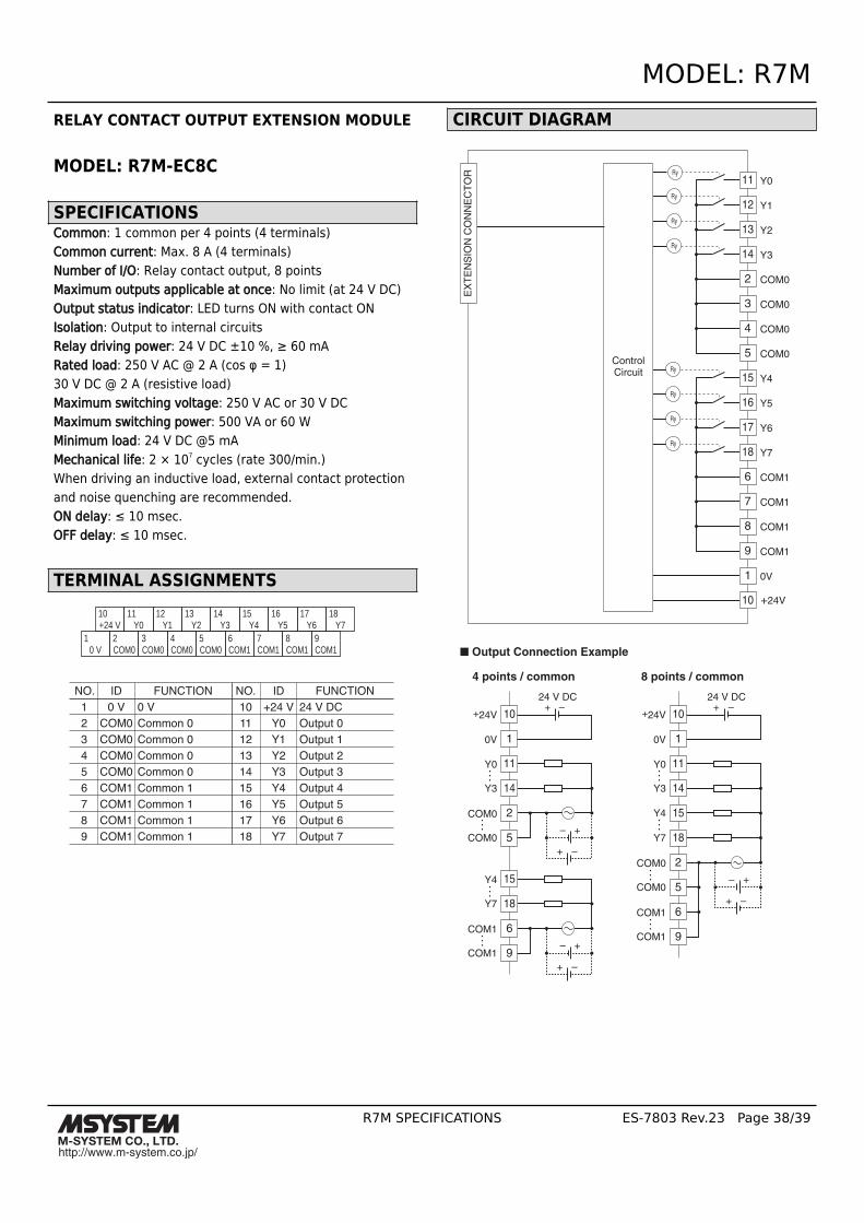
MODEL: R7M
R7M SPECIFICATIONS ES-7803 Rev.23 Page 38/39
http://www.m-system.co.jp/
RELAY CONTACT OUTPUT EXTENSION MODULE
MODEL: R7M-EC8C
SPECIFICATIONSCommon: 1 common per 4 points (4 terminals)Common current: Max. 8 A (4 terminals)Number of I/O: Relay contact output, 8 pointsMaximum outputs applicable at once: No limit (at 24 V DC)Output status indicator: LED turns ON with contact ONIsolation: Output to internal circuitsRelay driving power: 24 V DC ±10 %, ≥ 60 mARated load: 250 V AC @ 2 A (cos φ = 1)30 V DC @ 2 A (resistive load)Maximum switching voltage: 250 V AC or 30 V DCMaximum switching power: 500 VA or 60 WMinimum load: 24 V DC @5 mAMechanical life: 2 × 10⁷ cycles (rate 300/min.)When driving an inductive load, external contact protectionand noise quenching are recommended.ON delay: ≤ 10 msec.OFF delay: ≤ 10 msec.
TERMINAL ASSIGNMENTS
10+24 V
11Y0
12Y1
10 V
2COM0
3COM0
13Y2
4COM0
14Y3
5COM0
15Y4
6COM1
16Y5
7COM1
17Y6
8COM1
9COM1
18Y7
NO. ID FUNCTION NO. ID FUNCTION
1 0 V 0 V 10 +24 V 24 V DC
2 COM0 Common 0 11 Y0 Output 0
3 COM0 Common 0 12 Y1 Output 1
4 COM0 Common 0 13 Y2 Output 2
5 COM0 Common 0 14 Y3 Output 3
6 COM1 Common 1 15 Y4 Output 4
7 COM1 Common 1 16 Y5 Output 5
8 COM1 Common 1 17 Y6 Output 6
9 COM1 Common 1 18 Y7 Output 7
CIRCUIT DIAGRAM
10
14
1
2
5
11
+24V
24 V DC
Y0
0V
+
Y3
COM0
COM0
+ –
+–
18
6
9
15Y4
Y7
COM1
COM1
+ –
+–
10
14
1
2
5
11
+24V
24 V DC
Y0
0V
+ –
Y3
15Y4
18Y7
COM0
COM0
6
9
COM1
COM1
+ –
+–
–
ControlCircuit
10
5
1
2
6
4
7
13
8
9
14
12
15
11
16
17
18
COM0
COM0
COM0
Y0
Y1
Y2
Y3
COM0
COM1
COM1
COM1
0V
Y4
Y5
Y6
Y7
COM1
3
Ry
Ry
Ry
Ry
Ry
Ry
Ry
Ry
■ Output Connection Example
4 points / common 8 points / common
+24V
EX
TE
NS
ION
CO
NN
EC
TO
R

MODEL: R7M
R7M SPECIFICATIONS ES-7803 Rev.23 Page 39/39
http://www.m-system.co.jp/
Specifications are subject to change without notice.