0.123456 7689:;%5$6%? !%;?8=9456@$9a4 ... - … · in the case of a diode, for example, the symbol...
TRANSCRIPT

!"#$%"&#'()*+,-"$./,/"%,0.123"456""7689:;%"<8689=">5$6%?"
!"%;?8=9"456"@$9A4$#:A6$>8B8:C"
#'2D2*,/EE"

!"#"$%&'()#*&+($,%-#).($/&• 0"$%123/"*2*&• 4(-5123/"*2*&• 4(-5123/"*2*&6"78&&&1)92#&"$72#:($$2:.($/&
– ;<")&(#&=1)72*&78#(-%8&8(12>&• ?-1.1)92#&• @12A"512&)$*&B"%"*3C2A&• D"%8&42$/"79&E!'&
!"#$%&'(()&

0"%$)1/F&G#(-$*/F&0-==1"2/&
4"212:7#":&
0"$%123/"*2*&:($,%-#).($&
0"%$)1/F&G#(-$*/F&0-==1"2/&
0"%$)1/F&G#(-$*/F&0-==1"2/&
4"212:7#":&
4(-5123/"*2*&:($,%-#).($& ?)/H&
E#2=#2%I*"212:7#":&
+(#2&
!"#"$%&'()#*&+($,%-#).($/&?)/H&
7#>"#$%"7$#F$=;"89:65%A#:859"G2/"%;@5"&
82+-'/*HD'2&J$9&%((*&+J4&0(K6)#2&=#(<"*2/&:(L=1272&
212:7#($":/&*2/"%$&/(1-.($M&&&&@(#&42L(&=-#=(/2&"$&78"/&:(-#/2F&62&)#2&
-.1"N"$%&O#+J4&0(K6)#2M&&!2&6"11&=#(:22*&7(&-$*2#/7)$*&8(6&7(&*2/"%$&)&79=":)1&E+'&-/"$%&5-#$%"#G)+*-,&)$*&5-#$%"BGI'*+"L(*-12/M&
P&E12)/2&$(72Q&9(-&:)$&-/2&9(-#&(6$&/(K6)#2&7((1&)7&9(-#&"$/.7-.($&)$*&7#9&782&*2L(&(R&782&/9/72L).:&=#(:2//&/72=/&"11-/7#)72*&)$*&2A=1)"$2*&82#2M&

J$9&+J4&E#(<"*2/&&
S82&,#/7&/72=&"/&7(&5-"1*&782&/:82L).:&*")%#)L&(R&782&:"#:-"7F&)$*&1)9(-7&"/&-/2*&7(&*2/"%$&782&:"#:-"7&5()#*M&4-#"$%&78"/&=#(:2//F&L)$-R):7-#"$%&)/=2:7/&)#2&:($/"*2#2*&6"78(-7&R)"1M&

%,0.12"4J'K&S82&0:82L).:&+)=7-#2&7((1&"/&-/2*&7(&:#2)72&/:82L).:&-/"$%&)<)"1)512&/9L5(1/&R#(L&782&/9L5(1&1"5#)#"2/&)$*&"$72#:($$2:7&6"78&782&6"#2&7((1M&S8"/&L2)$/&9(-&)#2&)**"$%&*"T2#2$7&:(L=($2$7/&($&7(&9(-#&5()#*&)$*&:($$2:.$%&782L&6"78&6"#2/M&&
G2$2#)119F&782&R(11(6"$%&)#2&782&L)"$&:)72%(#"2/&(R&782&:(L=($2$7/&-/2*Q&
&PB2/"/7(#/F&+)=):"7(#/F&U$*-:7(#/&&&P4"(*2/F&S#)$/"/7(#/F&@VS/F&WV4/&&&P+($$2:7(#/F&D2)*2#/F&212:7#(L2:8)$":)1&:(L=($2$7/&&P4UE&U+/F&'GJ&U+/&)$*&(782#/&1"H2&X@YF&+0E&&

Figure Source: Wikimedia Commons
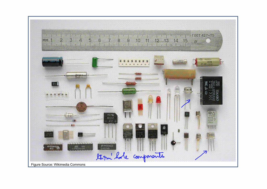
Figure Source: Wikimedia Commons
*+,,&-./01,&,234546&57.+8&97+&8,/7&0:+07;,&

+V4S&

U$&0:82L).:&782&/9L5(1/&68":8&62&-/2&)#2&UVVV&/9L5(1/&(#&JY0U&/9L5(1/&68":8&6"11&8)<2&($19&782&/9L5(1&<"26&6"78&$-L52#&(R&="$/F&$(7&782&):7-)1&/"N2&)$*&*"L2$/"($&(R&782&:(L=($2$7M&&&&&&&&&&&&&
&&&&&&&&&&&&&&&&&&&&&&&&&&&&&&
&&&&&
U$/.7-72&(R&V12:7#":)1&)$*&V12:7#($":&V$%"$22#/&;UVVV> &&&&&&JL2#":)$&&Y).($)1&07)$*)#*/&U$/.7-72&;JY0U>&&&&&&&&&&&&&
&&'(78&UVVV&)$*&JY0U&/9L5(1/&)#2&R-$:.($)119&782&/)L2M&&&
Z[W0\]&X-)*&^&"$=-7&JY4&G)72&
@(#&VA)L=12&

0(L2&')/":&'#()*&E#(:2//&072=/Q&&! &+(112:7&*)7)&/8227/&R(#&)11&:(L=($2$7/&78)7&6"11&52&-/2*M&! &S82&*2:"*2&68":8&R((7=#"$7/&$22*&7(&52&-/2*M&@((7=#"$7&"/&)&=):H)%"$%&<"26&(R&782&:(L=($2$7&78)7&"$:1-*2/&782&8(12/&78#(-%8&9(-#&5()#*&(#&=)*/&R(#&/-#R):2&L(-$7&*2<":2/M&_(-&6"11&,$*&0?S&R((7&=#"$7&)$*&S8#(-%838(12&R((7&=#"$7&R(#&:(L=($2$7/M&0212:7&782&R((7=#"$7&78)7&L227/&782&L2:8)$":)1`-"#2L2$7/&R(#&782&:(L=($2$7&78)7&9(-&8)<2&:8(/2$M&! &Ja):8&782&$)L2&(R&782&/212:72*&R((7=#"$7&&7(&782&:(L=($2$7&/9L5(1&59&2*".$%&782&=#(=2#.2/&R(#&2):8&:(L=($2$7M&&&! &b/"$%&‘=1):2&6"#2’&7((1&:#2)72&)&212:7#":)1&:($$2:.($&527622$&782&:(L=($2$7/&($&782&5()#*M&! &O$:2&9(-&:(L=1272&782&/:82L).:&9(-&8)<2&7(&%2$2#)72&782&$27&1"/7&)$*&"L=(#7&"7&7(&E+'&W)9(-7&7(&:(L=1272&782&5()#*&1)9(-7M&W)9(-7&6"11&)-7(L).:)119&"$/2#7&R((7=#"$7/&"$7(&782&5()#*&5)/2*&($&782&"$R(#L).($&%"<2$&2)#1"2#M&! &Y(6&=1):2&782&:(L=($2$7/F&*2,$2&=(62#&)$*&%#(-$*&=1)$2/F&#(-72&=89/":)1&6"#2/&-/"$%&78"/&7((1M&O$:2&782&5()#*&1)9(-7&"/&:(L=1272*&)$*&#(-.$%&(R&7#):2/&)#2&*($2F&62&:#2)72&72:8$(1(%9&,12/F&-$"<2#/)119&:)112*F&‘G2#52#&,12/’M&S82/2&)#2&-/2*&59&782&L)$-R):7-#2#&7(&=8(7(=1(7&782&L)/H/&)$*&L)$-R):7-#2&782&5()#*&782#2)K2#M&! &@"$)119&<2#"R9&782&5()#*&R(#&2##(#/c&<2#",:).($&"/&*($2&)1/(&)7&)11&/7)%2/M&

U$&)$9&/I6&7((1F&782&1"5#)#9&"/&782&82)#7&(R&782&7((1M&W"5#)#9&:($7)"$/&5(78&/:82L).:&/9L5(1/&)$*&=)#7&1"5#)#"2/&;R((7=#"$7/>M&
@(#&2A)L=12&/(L2&:(L=($2$7/&)#2&/8(6$&82#2&6"78&/9L5(1&)$*&R((7=#"$7&*27)"1/M&&! &&0:82L).:&/9L5(1&R(#&B2/"/7(#&"/&)<)"1)512&"$&/9L5(1&1"5#)#9&(R&O#+J4&+)=7-#2M&&! &&S8#-&8(12&)$*&0?4&R((7=#"$7/&)#2&)<)"1)512&"$&R((7=#"$7&1"5#)#9&(R&O#+J4&W)9(-7M&&&
&&&
&&&&&
&&&&&&&09L5(1&<"26&(R&B2/"/7(#&&&&&&&&&&E89/":)1&<"26&(R/"/7(#&6"78&*"L2$/"($/&&&&&&&&&&&&E):H)%"$%&<"26&(R&B2/"/7(#&
Example of CAD process using OrCAD (v9)

In the case of a diode, for example, the symbol pin names are given as 1 & 2 and Cathode & Anode. But in the package footprint pad names are given as C & A, 1 & 2. In case of mismatch of pin & pad names, edit either in the symbol library or footprint library to match the reference designations.
&&&&&&&&&&
&&&&&&&&&&&&&&&&&&&&
&&&&&&&&&&&&&&&&&&&&&&&&&&&&&&&&&&&&&&&&&&&
&&&&&&&&&&&&&&&&&&&&&&&&&&&&&
&&&&&&&&&&&&&&&&&&&&
&&&&&&&&&
&&&&&&&&&&&&&&&&&
&&&&&&
&&&&&&&&&&&&&&
In case of a Zener diode, the symbol pin count with footprint pad count does not match, say. Edit symbol to add missing pin by edit >part method.
&&&&
Figure Source: Wikimedia Commons

U$&:)/2&(R&7#)$/"/7(#/&782&/:82L).:&/9L5(1/&)#2=#2/2$72*&"$&78#22&*"T2#2$7&R(#L/&6"78&="$&$)L2/Q&2L"a2#F&5)/2F&:(112:7(#F&(#&+F'FV&(#&7829&:)$&52=#2/2$72*&6"78&$-L52#/&)/&dF^F&)$*&e&"$&/9L5(1&1"5#)#9M&J$*&7829&)#2&)1/(&)<)"1)512&)/&78#-’&8(12&)$*&0?4&=):H)%2/&"$&782&R((7=#"$7&1"5#)#9&(R&782&W)9(-7&L(*-12M&
&&&&S#)$/"/7(#&09L5(1&&&&&&&S8#(-%8&?(-$7&S#)$/"/7(#&&&&&&&&&&&&&&0?4&7#)$/"/7(#&
&&&&&&
&&&&&&&&&
&&&&&&&&&&&&&&&&&&&&&&&&&&&
&&
&&&&&&&
Figure Source: Wikimedia Commons
SO3e&
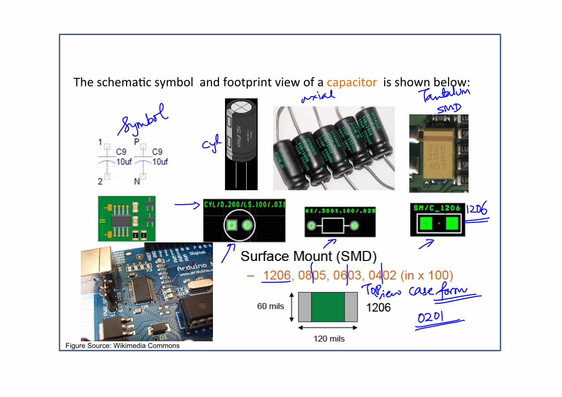
&&S82&/:82L).:&/9L5(1&&)$*&R((7=#"$7&<"26&(R&)&:)=):"7(#&&"/&/8(6$&521(6Q&&&&&&&&&&&&&&&&
&&&&&&&&&&&&&&&&&&&&&&&&&&&&&&&&&&&&&&&&&&&
&&&&&&&&&&&&&&&&&&&&&&&&&
&&
&&&&&&&&&&&
&&&&&&&&&&
&&&&&&&&&&&&
&&&&&
&&&&&&&&&&&&&&&&&&&&&&
&&&&&&&&&& & &&&&&&
&&&&&&&&&&&&&&&&&&&&&&&
Figure Source: Wikimedia Commons

&&&&&&&&&&&&&&&
&&&&&&&&&&&&&&&&&&&&&&&&&&&&&&&&&&&&&&&&&&&
&&&&&&&&&&&&&&&&&&&&&&&&&
&&
&&&&&&&&&&&
&&&&&&&&&&
&&&&&&&&&&&&
&&&&&
&&&&&&&&&&S8#-&8(12&L(-$7&U+& & & &&&&&&&&&0-#R):2&?(-$7&U+&&&&&&&&&&&&&&
&&&&&&&&&&&&&&&&&&&&&&
&&&&&&&&&& & &&&&&&
&&&&&&&&&&&&&&&&&&&&&&&
P4UE&/=2:",2/&4-)1&"$1"$2&=):H)%2&&&& &&&&&&&&&&&&&&P&0OG&"$*":)72/&/-#R):2&L(-$7&%-11&6"$%&:(L=($2$7&Pd\\&/=2:",2/&="7:8&527622$&782&76(&="$/&&&&&&&&&&&&&&&&&P&f\&/=2:",2/&="7:8&527622$&782&76(&="$/&Pd[&"$*":)72/&782&$-L52#&(R&="$/ &&&&&&&&&&&&&&P&d[&"$*":)72/&782&$-L52#&(R&="$/&P&!&)$*&W&"$*":)72/&782&6"*78&)$*&&&&&&&&&&&&&&&&&&&&&&&&&&&&&&&&P&!&)$*&W&"$*":)72/&782&&6"*78&)$*&12$%78&(R&&&&&12$%78&(R&782&:(L=($2$7M &&&&&&&&&&&&&&&&&&&&&&&&&&&&&&&&&&&&&&&&&782&&:(L=($2$7M&
&4UEMd\\Id[I!Me\\IWMZ\\&&&&&&&&&&&&&&&&&&&&& &&&&&&&0OGM\f\Id[I!GM^[[IWMe^f&
S82&R((7&=#"$7&"$R(#L).($&R(#&78#(-%8&8(12&)$*&0?4&U+/&)#2&*2,$2*&)/&521(6Q&&
Figure Source: Wikimedia Commons

EJ+gJGV&@OOSEBUYS&4VSJUW0&JBV&O'SJUYV4&@BO?&&4JSJ0DVVS0&O@&4VhU+V0&0bEEWUV4&'_&?JYb@J+SbBVB0&

<'-L.21"K.+M"#G)+*-,&

E#(i2:7&?)$)%2#&!"$*(6
42/"%$2#&!"$*(6
S((1&=)12a2&5-a($
Right side of your design window we can see tool palette button provides an electrical or graphical function, like adding wires and parts or placing graphic objects.

S(&/=2:"R9&)-7(L).:R2#2$:2&*2/"%$)7(#/&O=.($/j%(&7(&5)D'20j)-,N,-,2H,0j/212:7&(.0H,JJG2,'*0j&$*+'"6,N,-,2H,"j"2$)512&)-7(L).:)119R2#2$:2&=1):2*&=)#7/M
$//"H'()'2,2+0&7(&782&*2/"%$&59&/212:.$%&7JGH,&j7G-+&j&:8((/2`-"#2*&:(L=($2$7/&&&&&&&&&&&&&&&&&&&R#(L&*"T2#2$7&1"5#)#"2/M&&
O#&&&:1":H&782&E1):2&E)#7&7((1&($&782&7((1&=)12a2&&
When you place a part on a schematic page, the part can be placed without a reference designator assigned to it or it can be automatically assigned.

You can type a selective search string to instantly locate a specific part or search by using part search command.
Use Place>Wire from the place menu or click the wire tool on the tool palette for interconnecting components. You can cross the wires without connecting them.


To add additional schematic pages go to> Project manager window> select Schematic and right click for new page. You can name page by rename command.

A Schematic folder is simply a collection of schematic pages, which are logically connected by off-page connectors. Nets can be simply continued to the next page.
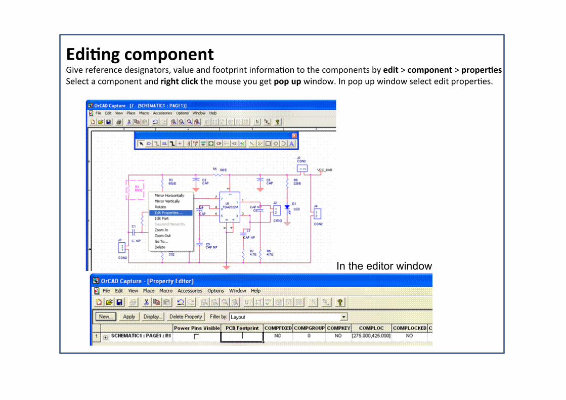
;/.D21"H'()'2,2+ G"<2R2#2$:2&*2/"%$)7(#/F&<)1-2&)$*&R((7=#"$7&"$R(#L).($&7(&782&:(L=($2$7/&59&,/.+&j&H'()'2,2+&j&)-'),-D,0" 0212:7&)&:(L=($2$7&)$*&-.1M+"HJ.HL&782&L(-/2&9(-&%27&)')"*)&6"$*(6M&U$&=(=&-=&6"$*(6&/212:7&2*"7&=#(=2#.2/M&
In the editor window

U$&78)7&/212:7&E+'&@((7=#"$7&:(1-L$&)$*&2$72#&782&$)L2&(R&782&R((7&=#"$7&1"H2&0?IBkd^\l&;78"/&"/&0?4&79=2&:(L=($2$7&R((7=#"$7>M&S82/2&R((7&=#"$7&$)L2/&)#2&)<)"1)512&"$&W"5#)#9&L)$)%2#
SAVE FILE File > Save as > file name .dsn

9,+J.0+"H-,GD'2 b/"$%&)&/:82L).:&:)=7-#2&7((1F&/-:8&)/&O#+J4&+)=7-#2F&_(-&:#2)72&)&W)9(-73&:(L=).512&$271"/7M&G(&7(")-'O,H+"(G2G1,-"K.2/'K"0,J,H+"+M,"/,0.12"PJ,"G2/"1'+'"S((1/"Q""HM''0,"+#2)72"Y271"/7&Q".2"#-,G+,"9,+J.0+"K.2/'K&0,J,H+"W)9(-7&G2/"1.R,"PJ,"2G(,"G2/")G+M"G2/",2GSJ,"B-$&V+O&7(&W)9(-7E&UR&9(-&:8)$%2&782&$271"/7&)K2#&5):H&)$$(7).$%&"$&W)9(-7&)$*&+)=7-#2F&W)9(-7’/&J-7(V+O&&-.1"79&)-7(L).:)119&&-=*)72/&&782&5()#*&,12M&

Introduction to Layout PCB Design/Layout Once the schematic is completed and approved by you, the PCB layout can be started. The following steps are performed to create the PCB: 5),2.21"BGI'*+ _(-&:)$&/7)#7&)&$26&*2/"%$&R#(L&W)9(-7’/&/2//"($&R#)L2&(#&R#(L&782&*2/"%$&
6"$*(6M& Next go to Start > Layout plus > select file > New >in load template file window type the .TCH file name (It can define the board layers, default grids, spacing, track widths, design rules) and select > Open.


In case of mismatch of pin & pad names edit the symbol and use it.
Note: Before we start doing any schematic select a right symbol and Footprint to the Component. The Symbol pin name & pin count should match with Footprint pad name and pad count. If you take a diode the symbol pin names are given as 1 and 2 and Cathode & Anode. But in the Footprint pad names are given as C & A, 1 & 2. Any parts not in the OrCAD Layout standard library are created at this time. Once the footprints have been inputted, they are randomly placed on the PCB.