01 chapter 3 02 additive processes for metals uncorrected
TRANSCRIPT

UN
CO
RR
EC
TE
D P
RO
OF
SPB-140376 Chapter ID 3 October 29, 2010 Time: 08:22pm Proof 1
01
02
03
04
05
06
07
08
09
10
11
12
13
14
15
16
17
18
19
20
21
22
23
24
25
26
27
28
29
30
31
32
33
34
35
36
37
38
39
40
41
42
43
44
45
Chapter 3
Additive Processes for Metals
David P. Arnold, Monika Saumer, and Yong-Kyu Yoon
Abstract Metals are vital building blocks for MEMS. Pure metals and metal alloys
AQ1
are employed in microsystem design to achieve a wide array of functionality.Common examples include electrical conductors, mechanical structures, magneticelements, thermal conductors, optical reflectors, and more. In this chapter, additiveprocesses for metals are discussed in the context of their application in MEMS.Particular attention is paid to MEMS-centric processing technologies, where thickmetal layers are often required. Basic guidelines are given for material selection,and fabrication recipes are provided as a starting point for process development.
3.1 Introduction
From the Bronze Age through the Iron Age, and even into modern times, met-als have fueled technological growth and played a key role in shaping society.All but 25 of the 120 elements on the periodic table are considered metals, andmany are naturally abundant on earth. Elemental metals are generally known toexhibit high electrical conductivity, high thermal conductivity, relatively high phys-ical density, and good mechanical ductility. In addition, metals can be combinedwith each other or with nonmetals to form innumerable metal alloy combinationswith diverse electrical, mechanical, magnetic, thermal, and optical material prop-erties. The availability, adaptability, and functionality of metals make them one ofthe most widely used engineering materials, not only at the macroscale, but also formicroscale applications.
D.P. Arnold (B)Department of Electrical and Computer Engineering, University of Florida, Gainesville, FL, USAe-mail: [email protected]
R. Ghodssi, P. Lin (eds.), MEMS Materials and Processes Handbook,MEMS Reference Shelf, DOI 10.1007/978-0-387-47318-5_3,C© Springer Science+Business Media, LLC 2011

UN
CO
RR
EC
TE
D P
RO
OF
SPB-140376 Chapter ID 3 October 29, 2010 Time: 08:22pm Proof 1
46
47
48
49
50
51
52
53
54
55
56
57
58
59
60
61
62
63
64
65
66
67
68
69
70
71
72
73
74
75
76
77
78
79
80
81
82
83
84
85
86
87
88
89
90
D.P. Arnold et al.
3.1.1 Overview
Metals are widely used for MEMS in many different functional roles. Metals areubiquitously used as electrical interconnections for their high electrical conductiv-ity. Metals also exhibit advantageous mechanical properties, so they are commonlyemployed as mechanical elements, both rigid structures and flexures. Metals arealso good thermal conductors, and thus attractive for thermal applications. Certainmetals exhibit ferromagnetic behavior and can be used to create or guide magneticfields. For optical applications, metals are used to provide reflective, mirrorlike sur-faces. Metal coatings are also used to encapsulate other materials, for example, toprevent oxidation or create hermetic seals, and thin interfacial metal layers act toenhance adhesion or prevent diffusion.
Material selection usually begins by identifying and prioritizing the desired mate-rial properties. For example, if a microstructure is intended as a mechanically strongelectrical conductor, one may begin by searching for materials with high electricalconductivity and high elastic modulus. Fortunately, bulk metals and metal alloyshave been widely studied for hundreds of years, and much of what is known aboutbulk material properties largely applies at the microscale. With the emergence ofmicroelectronics, MEMS, and nanotechnology, there is also a growing wealth ofknowledge about unique material behavior at the micro- and nanoscale.
Once a specific metal or class of metals is identified, the next step is to deter-mine how to fabricate and integrate the material into a microdevice. Although bulkmachining of metals is usually a top-down process (e.g. physical milling of a bulkpiece of metal), micromachining of metals is usually bottom-up (atom-by-atom,layer-by-layer deposition). Herein lies a major complication. For macroscale appli-cations, individual components are usually fabricated separately and then assembledtogether. The individual system components can be machined independently of oneanother. In MEMS fabrication, this is usually not the case; devices are manufac-tured in a sequential integrated fashion by selectively adding and subtracting layerson a planar substrate. This manufacturing approach places limitations on materialsand structure geometries. Furthermore, microfabrication creates a complex interplaybetween the fabrication process and the resulting material properties. These topicsare further discussed throughout this chapter.
Methods for metal deposition can be categorized into three groups: physicalvapor deposition (PVD), chemical vapor deposition (CVD), and electrochemicaldeposition (ECD). For MEMS, PVD and ECD are more commonly used, and thusare the primary focus of this chapter. Although CVD finds widespread usage insemiconductor devices and integrated circuits for conformal deposition of thin metalfilms, it is not as popular for MEMS fabrication because of film thickness limitationsand process complexity.1
The remainder of Section 3.1 discusses general tradeoffs for the various fab-rication approaches available for depositing metals and metal alloys. Section 3.2
1See Chapter 2 (specifically Section 2.3) for general information on CVD. UN
CO
RR
EC
TE
D P
RO
OF
SPB-140376 Chapter ID 3 October 29, 2010 Time: 08:22pm Proof 1
91
92
93
94
95
96
97
98
99
100
101
102
103
104
105
106
107
108
109
110
111
112
113
114
115
116
117
118
119
120
121
122
123
124
125
126
127
128
129
130
131
132
133
134
135
3 Additive Processes for Metals
provides a more detailed discussion of PVD methods for metals, including evapo-ration, sputtering, and pulsed-laser deposition. Section 3.3 describes ECD methods,including both electroplating and electroless plating. Section 3.4 describes LIGAand UV-LIGA processes, a key technological advancement in the history of MEMS.Finally, Section 3.5 presents material properties and process selection guidelines formetals.
3.1.2 Fabrication Tradeoffs
There are many fabrication-related tradeoffs that must be considered for microma-chining of metals. The final material properties of a metal are often highly dependenton the film thickness, deposition method, and specific processing conditions. Thiscreates interesting design/fabrication/integration challenges and compromises. Inaddition, because of these geometrical and process dependencies, the material prop-erties for metal films reported in the literature vary widely. Thus, although basicstarting recipes may be found (and many are provided below), some process devel-opment is usually required for fine-tuning of the metal properties to meet a specificneed.
In addition to differing material properties, various fabrication methods yielddifferent microstructural features and process integration issues. For example, evap-oration usually results in poor step-coverage but high film purity. Sputtering, onthe other hand, can provide good sidewall coverage, but with lower film purity.PLD often affords high deposition rates, but is usually limited in deposition area.In contrast to these PVD methods, electroplating and electroless plating rely onchemically “growing” the metals. This enables selective deposition (e.g. using pho-toresist masks) only where needed, thus avoiding additional process steps and timerequired for film patterning via post-deposition chemical etching2 or liftoff.3 Inaddition, the material waste (overage) associated with PVD can have significantcost implications, especially for thick layers of expensive precious metals.
The required film thickness also affects fabrication process selection. For exam-ple, thinner metal films may be used as coatings or as interfacial layers. In contrast,to better conduct heat or to provide heftier mechanical structures, thicker metal filmsmay be required. Evaporation and electroless plating are better suited for thinnerfilms (e.g. less than 1 µm), whereas thicker films demand the faster deposition ratesafforded by sputtering, PLD, or electroplating. For commercial manufacturing, thereare also numerous tradeoffs involving cost, throughput, reliability, and repeatability.
The deposition of alloys raises additional issues. Different alloy ratios are oftenrequired to enhance a material property such as electrical resistance, mechanicalhardness, magnetic permeability, and the like. In cases where a very specific alloy
2See Chapters 7 and 8 for more information on chemical etching.3See Chapter 9 (specifically Section 9.2.5.5) for more information regarding liftoff.

UN
CO
RR
EC
TE
D P
RO
OF
SPB-140376 Chapter ID 3 October 29, 2010 Time: 08:22pm Proof 1
136
137
138
139
140
141
142
143
144
145
146
147
148
149
150
151
152
153
154
155
156
157
158
159
160
161
162
163
164
165
166
167
168
169
170
171
172
173
174
175
176
177
178
179
180
D.P. Arnold et al.
ratio is required, stoichiometric control is a major consideration. Reliably main-taining a specific alloy ratio over long periods of time is critical for repeatable,large-scale manufacturing. In addition to repeatability and control, there is anotherimportant fabrication-related aspect for alloys: the ability (or inability) to vary thealloy ratio. This is especially important for process development and for fine-tuningof alloy composition. Moreover, deposition methods that permit on-the-fly alloycontrol can be used to create graded alloys, multilayers, or other complex structures.
The different metal deposition methods offer varying degrees of alloy con-trol. Evaporation of alloys is often discouraged because of the disparate andhighly temperature-dependent vapor pressures of different metal constituents. Thismakes control of alloys difficult with conventional evaporation systems. In con-trast, sputtering and PLD permit deposition of many different alloys with fairlyrepeatable alloy control, but adjusting the alloy ratio requires changing the metaltarget. This can create time-consuming and costly process development cycles. Forelectroplating, the alloy ratio can sometimes be readily adjusted by varying the elec-troplating current density without strong influence on the properties of the deposit.Unfortunately, the alloy ratio may also be sensitive to other process conditions suchas pH, temperature, or stirring, so repeatability is sometimes difficult. Electrolessplating is less commonly used for alloy deposition because of the complex inter-dependent factors that determine the composition. See Table 3.1 for a generalsummary.
Table 3.1 General tradeoffs for metal deposition
Fabricationprocess
Depositionrate
Depositionarea Film purity Alloy control
Equipmentcomplexity
Evaporation Slow Very large High Poor ModerateSputtering Moderate Large Moderate Good HighPLD Moderate Small High Good HighElectroplating Fast Large Moderate Fair LowElectroless
platingModerate Large Moderate Fair Very low
3.2 Physical Vapor Deposition
Physical vapor deposition (PVD) methods rely on the physical transfer of metalatoms from a metal source to the wafer substrate, unlike chemical methods, whichemploy a chemical reaction. Different physical phenomena can be used to drive theprocess, as described below.
3.2.1 Evaporation
Evaporative deposition, or more commonly just “evaporation,” is a fairly straightfor-ward method for metal deposition. The basic concept is to heat a metal sufficientlyto create a vapor, which diffuses and recondenses in solid form on other surfaces.
UN
CO
RR
EC
TE
D P
RO
OF
SPB-140376 Chapter ID 3 October 29, 2010 Time: 08:22pm Proof 1
181
182
183
184
185
186
187
188
189
190
191
192
193
194
195
196
197
198
199
200
201
202
203
204
205
206
207
208
209
210
211
212
213
214
215
216
217
218
219
220
221
222
223
224
225
3 Additive Processes for Metals
This process is usually performed in high-vacuum conditions (below 10−5 torr) soas to limit gaseous molecular scattering and to create a high-purity process envi-ronment. Note that, although the metal to be evaporated is obviously very hot, thewafer substrate usually remains at room temperature, unless intentionally heatedor cooled. Also, because of the very low chamber pressures, the metal vapor tendsto follow a straight path, leading to very directional deposition and poor sidewallcoverage.
A typical system comprises a process chamber, a vacuum system, and a metalheating system, as shown in Fig. 3.1. Wafers are usually mounted upside down ona hemispherical chamber ceiling, which may include a planetary system to rotatethe wafers for improved uniformity. The metal to be deposited – known as the“charge” – is placed in metal “boat” or ceramic crucible. The chamber is then closedand evacuated to a base pressure of 10−6 torr or lower. Then, the metal is heated usu-ally to 500–2500◦C (depending on the metal) to increase the vapor pressure. After awarm-up period, a physical shutter is used to precisely start and end the depositiononto the wafers. A quartz crystal microbalance (QCM) mounted inside the chambermonitors the deposition, and can provide feedback signals for automated control.
Fig. 3.1 Schematic of evaporation system
3.2.1.1 Thermal Evaporation
The simplest evaporation systems use joule heating to heat the metal charge. Thedissipative heat can be created by direct conduction currents or magnetic-field-induced eddy currents. In the simpler conductively heated systems, high currentsare passed through wound coils or a small metal boat (usually tungsten), insideof which sits the charge. The resistive heating of the boat facilitates deposition ofrelatively low-melting-point metals such as Ag, Al, and Au.
Evaporation of higher-melting-point refractory metals such as Ta, W, Mo, and Tiis challenging because these require very high temperatures to achieve reasonablevapor pressures and deposition rates [1]. Because of this, the use of metal boats anddirect conductive heating may not be permissible. Instead inductive heating can beused where the metal sits in a ceramic crucible that is surrounded by a coil. RF

UN
CO
RR
EC
TE
D P
RO
OF
SPB-140376 Chapter ID 3 October 29, 2010 Time: 08:22pm Proof 1
226
227
228
229
230
231
232
233
234
235
236
237
238
239
240
241
242
243
244
245
246
247
248
249
250
251
252
253
254
255
256
257
258
259
260
261
262
263
264
265
266
267
268
269
270
D.P. Arnold et al.
excitation of the coil is used to induce eddy currents in the metal. This approachpermits a wider range of metals, but the crucible itself may become very hot, whichcan result in contamination.
3.2.1.2 E-Beam Evaporation
Another configuration for evaporation uses a directed electron beam to bombardthe metal charge. The electron beam source is usually underneath the metal charge.Strong magnetic fields are used to steer the electron beam in a 270◦ circular arc toimpinge on the charge. Although more complicated, the advantage of this approachis that the electron beam heats a central portion of the charge: the outer area of thecharge and crucible remain at lower temperatures, so as to minimize contamination.
3.2.1.3 Issues with Alloys
Evaporation of alloys with precise alloy composition can be quite challenging. Thebasic problem is that evaporation relies on heating to increase the vapor pressureand thus control deposition rate. The vapor pressure and deposition rate of an ele-mental metal are usually very sensitive to temperature, and different metals requirevastly different temperature ranges for evaporation. For single-element deposition,precise control of the deposition rate is relatively unimportant, so long as the finalfilm thickness is controlled. This is easily accomplished using a QCM to stop thedeposition process at the predetermined film thickness.
Consider, however, deposition of a binary alloy. In a single-source system, ametal alloy can be used as the charge, but at a given temperature, the two metalsin the alloy will evaporate at different rates, resulting in a different alloy ratio in thedeposited layer. Attempts can be made to compensate for this, but impracticablyprecise temperature control may be required. Another approach is to coevapo-rate different metals from independently heated crucibles. This allows independentcontrol of the evaporation rates, but because of the temperature sensitivity of theevaporation process, and the inability to monitor the independent evaporation rateseasily, precise alloy control remains very challenging. One alternative is to create amultilayer stack by alternating deposition of the constituent elements. After depo-sition, a heat treatment can be used to interdiffuse the metals to form the desiredalloy. This approach, however, is more complicated, more time-consuming, andrequires a substrate that can withstand the high-temperature postdeposition heattreatment.
It should be noted that graded alloys or multilayers can be easily achieved usinga multisource evaporation system. However, because of the difficulty of alloy con-trol, evaporation is better suited for pure metals or for metal alloys where precisecomposition is not necessary.
3.2.2 Sputtering
Sputtering is a physical process or phenomenon, where accelerated ions, usuallyAr+, knock out atoms in a solid target by bombardment in a potential gradient
UN
CO
RR
EC
TE
D P
RO
OF
SPB-140376 Chapter ID 3 October 29, 2010 Time: 08:22pm Proof 1
271
272
273
274
275
276
277
278
279
280
281
282
283
284
285
286
287
288
289
290
291
292
293
294
295
296
297
298
299
300
301
302
303
304
305
306
307
308
309
310
311
312
313
314
315
3 Additive Processes for Metals
environment. During the bombardment, momentum exchange occurs between theions and the atoms of the surface of the target. The energized atoms are volatile andspread out as a vapor to land on the vicinity surface and the sample substrate. Thesputtering process requires a vacuum environment, which is prepared by pumpingout a stainless steel chamber enclosing the anode, the cathode, the target, the sub-strate, and so on. The chamber is evacuated to a base pressure of 10−6 torr or lower.Then a bombardment gas, usually Ar, is introduced to the chamber and maintainedaround 1–10 mtorr level. The Ar gas is ionized into Ar+ by applying bias voltagebetween the anode and the cathode. Depending on the voltage waveforms used, thesputtering process is categorized as either direct current (DC) sputtering or radiofrequency (RF) sputtering, as shown in Fig. 3.2.
(a) (b)
Fig. 3.2 Schematics of (a) DC and (b) RF sputtering systems
Thisfigurewill beprintedin b/w
To obtain uniform thickness of a thin-film metal layer, mechanical movementsuch as rotation of the substrate holder can be used during the sputtering process.The rotational speed of the stage ranges from 10 to 30 rpm. The deposition rate is afunction of many parameters including target-to-substrate distance, ion energy, themass of the ion species, the mass of the target material, and the like [2].
3.2.2.1 DC Sputtering
For the sputtering of electrically conductive materials such as Al, Ti, Cr, Cu, Ag, Au,Pt, and W, a DC power source is used to energize the Ar+ ions to bombard the targetmaterial placed on the cathode. The DC sputtering system, as depicted in Fig. 3.2a,consists of the DC power supply, cathode, a metal target attached to the cathode,Ar+ plasma generated by high-voltage application, and an anode on which a samplewafer can be placed. The negatively biased metal target is bombarded by argon ionsfrom the plasma, ejecting one or more metal atoms. Some of these ejected atoms are

UN
CO
RR
EC
TE
D P
RO
OF
SPB-140376 Chapter ID 3 October 29, 2010 Time: 08:22pm Proof 1
316
317
318
319
320
321
322
323
324
325
326
327
328
329
330
331
332
333
334
335
336
337
338
339
340
341
342
343
344
345
346
347
348
349
350
351
352
353
354
355
356
357
358
359
360
D.P. Arnold et al.
transported and deposited on the substrate wafers. The deposition rate is increasedas the sputtering power is increased, however, too much power causes damage onthe substrate. To counteract this effect, magnetron sputtering has been introduced toincrease the deposition rate. A magnet placed behind the target creates a field thatguides electron movement near the target, causing more efficient ionization of Arwithout excessively high voltages.
3.2.2.2 RF Sputtering
As an alternative to the DC supply, RF power systems can be used, as shown inFig. 3.2b. The RF sputtering system also requires a DC bias voltage to generateplasma. After plasma is generated, however, the major driving force acting on theargon ions is exerted by the alternating current source. Typically the 13.56 MHzindustry, science, and medicine (ISM) frequency band is used. Because alternatingcurrents can flow across dielectric materials, RF sputtering systems can deposit notonly electrically conducting materials, such as metals, but also dielectric materials,such as SiO2, Si3N4, and glass, which are not achievable with DC sputtering due tocharging effects. Also, by reversing the electrical connections, the substrate can bebombarded as opposed to the metal target. This process is often used to clean thesubstrate surface before depositing the target material.
3.2.2.3 Step Coverage
In contrast to the evaporation process, sputtering provides reasonably conformalcoatings on uneven surfaces. This is particularly useful for the metallization of three-dimensional (3-D) MEMS structures as well as the metal interconnect of integratedcircuits. The step-coverage of a sputtered thin film in a via hole has been calcu-lated [3, 4], where the profile shows a high deposition rate on the top surface and alow deposition rate on the sidewall. As a result, the sidewall thickness tapers downtoward the bottom. For a very high aspect ratio, the bottom portion may not havesufficient metal coverage due to limited mass transfer into the narrow entrance of thevia hole and the higher pressure environment in the chamber. This effect is depictedin Fig. 3.3. This kind of poor coverage is more significant in high-aspect-ratio viasor trenches as compared to high-aspect-ratio pillars or walls.
The step coverage can be improved by substrate heating to enhance surfacediffusion or by applying an RF bias to the wafers to introduce surface bombard-ment resulting in redeposition on the sidewalls [1]. The heating approach may beapplicable to the metal interconnect process for ICs, where the insulating layeris a temperature-tolerant material such as SiO2, however, it may not be directlyapplicable for the metallization of 3-D MEMS structures where the structural mate-rial is often a temperature-intolerant polymer. Step-coverage of thin films for veryhigh-aspect-ratio MEMS structures remains a challenging area. Alternatively, elec-troless plating may be used for the thin film metallization of such high-aspect-ratiopolymeric structures. U
NC
OR
RE
CTE
D P
RO
OF
SPB-140376 Chapter ID 3 October 29, 2010 Time: 08:22pm Proof 1
361
362
363
364
365
366
367
368
369
370
371
372
373
374
375
376
377
378
379
380
381
382
383
384
385
386
387
388
389
390
391
392
393
394
395
396
397
398
399
400
401
402
403
404
405
3 Additive Processes for Metals
Fig. 3.3 Sputtered metaldeposition in a densely placedhigh-aspect-ratio structure
Thisfigurewill beprintedin b/w
3.2.2.4 Other Issues in Sputtering
One concern in thin-film deposition using sputtering (or evaporation) on a thick3-D polymeric layer is that the residual solvent or moisture tends to degas underhigh vacuum conditions, resulting in poor adhesion between the polymer andthin-film metal layer. To prevent degassing effects, an additional hardbake step isrecommended before the sputtering or evaporation process can be used.
One feature found in many sputtering systems is the ability to “clean” the sub-strate before the metal deposition by sputter etching. This cleaning step can improveadhesion of the metal. Sputter etching can be implemented either by reversing theelectrical connections or by placing negative bias on the substrate with respect tothe plasma, resulting in increasing ion bombardment on the substrate. Increasingthe incident ion energy increases the adatom (Ar ion) mobility, which can aid incleaning the deep sidewalls of a 3-D structure, thereby improving step-coveragein deep-etched features [5]. However, high sputter etch rates may cause substratedamage.
Although sputtering of alloy is commonplace, there are several important issuesand approaches. In sputtering, the deposited film composition is usually fairly closeto that of the bulk target, so alloys can be rather easily obtained. However, differentelements in the target alloy may exhibit different sputter yields, causing composi-tion variation. To achieve better control of stoichiometry, a multiple target systemmay be used, where the power of each target can be individually controlled to alterthe final composition of the alloy layer. Also, by using a composite target with dif-ferent regions of concentration or by changing electrical properties of the plasma,the composition of the deposited layer can be controlled [6].
Moreover, sputtered compounds can intentionally have a very different com-position from the sputter target by adding reactive gaseous precursors during thedeposition. Reactive sputtering is a process in which the normally inert sputter gas isreplaced by an inert/reactive mixture [1]. For example, TiN, one of the most populardiffusion barrier layers in IC fabrication, can be deposited using reactive sputter-ing. By controlling the partial pressure of nitrogen in the sputtering system, thecomposition of TiN can be controlled.

UN
CO
RR
EC
TE
D P
RO
OF
SPB-140376 Chapter ID 3 October 29, 2010 Time: 08:22pm Proof 1
406
407
408
409
410
411
412
413
414
415
416
417
418
419
420
421
422
423
424
425
426
427
428
429
430
431
432
433
434
435
436
437
438
439
440
441
442
443
444
445
446
447
448
449
450
D.P. Arnold et al.
Stress is also an important issue for sputtered films. A thin film deposited on asubstrate is subjected to either tensile or compressive stress as influenced by the baselayer and deposition conditions. One component of the stress – known as extrin-sic stress – is due to thermal expansion mismatch of the film with the substrate.This stress may be significant if the wafer temperature varies (intentionally or unin-tentionally) from room temperature during the film deposition. In addition, largeintrinsic stresses may also occur depending on deposition rate, film thickness, andthe background chamber environment. In many cases, efforts are made to minimizethese stresses. Alternatively, for MEMS devices, these stresses can be put to gooduse to realize devices such as bimorph actuators or stress-engineered 3-D structures[7, 8].
3.2.3 Pulsed Laser Deposition
Pulsed laser deposition (PLD) is another method for depositing metals, althoughmuch less often used for MEMS. As shown in Fig. 3.4, the system uses a high-energy laser beam (typically 108 W/cm2) to strike a metal target within a vacuumchamber. The laser beam melts, evaporates, and ionizes a region of the target. Thisablation process creates a vapor plume that transfers material to the sample wafer.
One major advantage of PLD for MEMS applications is precise stoichiome-try/composition control and relatively fast deposition rates. Ideally the depositedmaterial possesses the same chemical composition as the metal target. High qualitycrystalline deposits are also possible with substrate heating. The biggest drawbackis that most PLD systems can only provide uniform deposition over a small surfacearea, sometimes only about one square centimeter. This decreases the utility of PLDfor volume manufacturing. Despite this drawback, PLD finds application where
Fig. 3.4 Schematic of pulsed laser deposition system UN
CO
RR
EC
TE
D P
RO
OF
SPB-140376 Chapter ID 3 October 29, 2010 Time: 08:22pm Proof 1
451
452
453
454
455
456
457
458
459
460
461
462
463
464
465
466
467
468
469
470
471
472
473
474
475
476
477
478
479
480
481
482
483
484
485
486
487
488
489
490
491
492
493
494
495
3 Additive Processes for Metals
precise stoichiometric control is paramount, especially for complex multielementmaterials. For metallic systems, this alloy control is beneficial for realizing high-performance magnetic materials and superconductors. PLD also finds widespreadapplication for many other complex nonmetallic films, such as oxides, nitrides, andsemiconductors.
The exact process and resulting film composition and structure are dependent onthe laser parameters, chamber pressure/atmosphere, sample temperature, and sam-ple surface quality. The complex physical and chemical interactions are the subjectof ongoing research.
3.3 Electrochemical Deposition
Electrochemical deposition involves the reduction of metal ions from aqueous,organic, or fused-salt electrolytes. The reduction of metal ions Mz+ in aqueoussolution is represented by
Mz+ (metal ion in solution) + z e− (electrons) → M (metal deposit)
Two processes can be used to provide the electrons for the reduction reaction:(1) electroplating (or electrodeposition), where an external power supply providesthe electrons, or (2) electroless deposition, where a reducing agent provides theelectrons.
In MEMS electrochemical deposition is commonly used to deposit surfacecoatings, or in the case of electroforming, for producing an entire microstructureor device. In electroforming, microstructured molds of different materials (e.g.,polymers/resist, silicon) are electrochemically filled with metals such as nickel,copper, gold, or various metal alloys. More details can be found in Section 3.4.
3.3.1 Electroplating
The material properties of electroplated metals or alloys are strongly influencedby the chemistry of the electrolyte (e.g., type and concentration of ions, pH, typeof additives), the physical parameters of the process (e.g., temperature, fluidics,current), and the property of the substrate (surface quality, shape). Depending onthe metal to be plated and/or on the shape of the desired microstructures, theelectroplating process has to be adapted to the specific application. The basics ofelectrochemical deposition can be found in several excellent books (e.g., [9–11])and are summarized in this section. In addition, starting recipes are provided forsome of the most common electroplated metals for MEMS: nickel, copper, gold,and some nickel alloys.
3.3.1.1 Electrochemical Reactions
The general setup and operation of an electrochemical deposition cell are shown inFig. 3.5. Two electrodes are immersed into an electrolyte. By applying an electric

UN
CO
RR
EC
TE
D P
RO
OF
SPB-140376 Chapter ID 3 October 29, 2010 Time: 08:22pm Proof 1
496
497
498
499
500
501
502
503
504
505
506
507
508
509
510
511
512
513
514
515
516
517
518
519
520
521
522
523
524
525
526
527
528
529
530
531
532
533
534
535
536
537
538
539
540
D.P. Arnold et al.
current, reduction (electron uptake) takes place at the cathode, and oxidation (elec-tron liberation) occurs at the anode. In the case of electroplating, the substrate servesas the cathode, and metal ions are reduced to form a solid lattice. The anode can besoluble, meaning it is dissolved via oxidation during the electroplating process. Thetwo partial reactions are expressed by the following equations.
Fig. 3.5 Schematic of ageneral electrochemicaldeposition cell (using solubleanode)
Reduction (cathode): Mz+ + z e− → M
Deposition of metalOxidation (anode): M → Mz+ + z e−
Dissolution of metal (for a solubleanode)
The steady oxidation of the anode (a metal to be deposited) ensures a constantreplenishment of metal ions in the electrolyte. Sometimes inert anodes such as plat-inum are used, for example, in gold electroplating. In this case, replenishment ofmetallic ions in the electrolyte is solely provided by manual addition of metal saltsto the plating bath.
The theoretically deposited mass mtheo can be calculated from the electrochemi-cal Faraday’s law as
mtheo =M∗I∗t
z∗F(3.1)
where M = Molar mass the deposited metal; I = Current; t = Time z =
Valency; F = Faraday constantOther reactions also can occur due to decomposition of water. By the oxidation of
water, oxygen gas can be produced at the anode. By the reduction of water, hydrogen UN
CO
RR
EC
TE
D P
RO
OF
SPB-140376 Chapter ID 3 October 29, 2010 Time: 08:22pm Proof 1
541
542
543
544
545
546
547
548
549
550
551
552
553
554
555
556
557
558
559
560
561
562
563
564
565
566
567
568
569
570
571
572
573
574
575
576
577
578
579
580
581
582
583
584
585
3 Additive Processes for Metals
gas can be released at the cathode. Other components of the electrolyte can also reactat the electrodes. The overall current is thus distributed to these different reactions.The percentage of the total current associated with the reduction of metal is definedas the cathodic current efficiency γ and can be calculated by the quotient of theeffective deposited mass meff and the theoretical deposited mass mtheo,
γ =m eff
m theo. (3.2)
If hydrogen production at the cathode cannot be suppressed, it usually severelyreduces the current efficiency of the deposition process. Another adverse effect is therise of the pH at the electrode surface, which leads to the buildup and incorporationof metal hydroxides into the deposits, leading to a brittle deposit. The accumula-tion of hydrogen bubbles, which adhere on the surface, can also cause pores in thedeposit.
3.3.1.2 Deposition Process
In the bulk electrolyte, cations are enclosed in a complex shell. This complex shellconsists of water molecules (hydration shell) or other complexing agents such assulfite or cyanide. Before applying a current, the ion concentration is homogeneousat the electrode surface and in the bulk solution. When applying a current, the metalion is consumed at the electrode, and this depletion region extends farther away intothe bulk as the deposition proceeds.
Movement of the complexed metal ions in the electrolyte is governed by threedifferent mass transport mechanisms: migration, convection, and diffusion. In mostdeposition processes the conductivity of the electrolyte is relatively high, and theapplied potentials are moderate. As a consequence, most of the electrical fielddrops across the electrical double layer in front of the electrodes, and field-inducedmigration is minimal. Therefore the predominant transport mechanisms are usuallyconvection (due to stirring or agitation), which dominates in the bulk electrolyte,and diffusion, which dominates near the surface of the electrodes.
The reduction of the metal ions at the cathode is very complex and can be dividedinto four parts: (1) diffusion of the solvated or complexed metal ions from the bulksolution to the electrode surface, (2) dehydration and transport of the cations throughthe electric double layer, (3) cationic reaction at the solution–solid interface (ionuptake and electron transfer), and (4) surface migration and incorporation of theadsorbed metal atoms into the metal lattice. Figure 3.6 depicts the overall process.
The ion diffusion is described as follows. The region immediately next to thecathode is characterized by a fictitious Nernst diffusion layer, where the gradientof ion concentration is assumed constant, as shown in Fig. 3.7. The thickness ofthis layer δ is strongly influenced by convection (agitation) in the electrolyte, butis typically on the order of tens to hundreds of micrometers. In stirred electrolytesthe thickness of the diffusion layer will be determined by this forced convection,whereas in unstirred electrolyte baths the diffusion layer increases with time.

UN
CO
RR
EC
TE
D P
RO
OF
SPB-140376 Chapter ID 3 October 29, 2010 Time: 08:22pm Proof 1
586
587
588
589
590
591
592
593
594
595
596
597
598
599
600
601
602
603
604
605
606
607
608
609
610
611
612
613
614
615
616
617
618
619
620
621
622
623
624
625
626
627
628
629
630
D.P. Arnold et al.
bulk solution
+++
diffusion layerelectric
double layer
cathode
(1)(2)
(4)
electron
+ cation
+++
water molecule
or complexing agent
+++
(3)
Fig. 3.6 Schematic diagram of the electrochemical deposition process
The deposition rate can be enhanced by increasing the current density, up untilthe ion concentration at the cathode approaches zero. The current density at whichthis occurs is called the limiting current density. The limiting current density (andhence maximum deposition rate) can generally be increased by increasing thecation concentration; by increasing the temperature, thus increasing the diffusioncoefficient; and by increasing the convection (e.g., stirring the solution), result-ing in a smaller diffusion layer. Modifying the electrolyte chemistry, especially viacomplexing agents, can also influence the limiting current density.
In the case of pulse-plating, the pulse current density is limited by the depletionof ions in the pulsation layer, whereas the average current density is limited by theconcentration gradient in the outer stationary diffusion layer. Thus two diffusionlayers can be defined: a pulsation layer in the immediate vicinity of the cathode anda stationary layer up to the point where the mass transfer is controlled by convection.
Once the cations reach the cathode surface by means of mass transfer, there isanother barrier to overcome before they lose charge and are incorporated into thecrystal lattice. That barrier is called the electric double layer. The simplest model ofthe double layer structure is given by the Helmholtz model, as depicted in Fig. 3.8.The double layer represents an organized arrangement of positive ions from thesolution to compensate for the negative charges on the surface, forming an interfaceregion similar to a parallel plate capacitor. The thickness of this layer is on the orderof a few nanometers [12]. The cations to be deposited have to penetrate through theelectric double layer, where they shed their hydration (or complex) shell. Then theyacquire electrons in the reduction process and become adsorbed adatoms.
The final step in the formation of a crystalline metal deposit is the incorporationof the adatoms into the lattice. The adatoms are preferentially incorporated at activelattice sites such as grain boundaries, imperfections, or pre-existing built-up adatom U
NC
OR
RE
CTE
D P
RO
OF
SPB-140376 Chapter ID 3 October 29, 2010 Time: 08:22pm Proof 1
631
632
633
634
635
636
637
638
639
640
641
642
643
644
645
646
647
648
649
650
651
652
653
654
655
656
657
658
659
660
661
662
663
664
665
666
667
668
669
670
671
672
673
674
675
3 Additive Processes for Metals
(a)
(b)
Fig. 3.7 Concentration of metal ions as a function of distance from the cathode (a) for directcurrent plating and (b) for pulse current plating
clusters on the surface. If the adsorption of an adatom ensued away from an energet-ically stable position, surface diffusion may transport the adatom to another activelattice site on the surface. The process of either building new grains (nucleation) orcontributing to the growth of existing grains defines the formation of metal depositsin electroplating. Additional inhibitors in a plating bath can influence this nucleation

UN
CO
RR
EC
TE
D P
RO
OF
SPB-140376 Chapter ID 3 October 29, 2010 Time: 08:22pm Proof 1
676
677
678
679
680
681
682
683
684
685
686
687
688
689
690
691
692
693
694
695
696
697
698
699
700
701
702
703
704
705
706
707
708
709
710
711
712
713
714
715
716
717
718
719
720
D.P. Arnold et al.
Fig. 3.8 Helmholtz model ofthe electric double layer. X HPouter Helmholtz plane; q−
M
negative-charged metalsurface; q S positive-chargedsolution side of the interface
and therefore the growth processes that affect the properties of the deposit such ashardness, internal stress, and so on.
3.3.1.3 Overpotential
In the equilibrium condition (absence of external current), the potential of an elec-trode is denoted as Eh. As a result of a current flowing through the electrolyte thepotential of the given electrode is changed to E. The difference between these twopotentials is defined as overpotential
η = E − Eh (3.3)
The overpotential arises from the different electrochemical mechanisms associ-ated with the reactions and movement of the ions or adatoms. The total overpotentialis the sum of the individual overpotentials associated with each of these mecha-nisms. As a result, any one can be rate-determining for the electrodeposition. Thediffusion overpotential ηdiff arises due to mass transport through the diffusion layer.If this step is the slowest, the reaction is called diffusion-controlled. The activationoverpotential ηact is associated with transfer of ions and electrons across the electricdouble layer and the transfer of the electrons. Therefore ηact is directly related to theelectrode material. If the ion and electron transfer at the metal–solution interface isthe most inhibiting step, the process is considered activation-controlled. The processby which the uncharged adatoms either form new grains or contribute to the growthof existing grains is associated with the crystallization overpotential ηcrys. Ohmic U
NC
OR
RE
CTE
D P
RO
OF
SPB-140376 Chapter ID 3 October 29, 2010 Time: 08:22pm Proof 1
721
722
723
724
725
726
727
728
729
730
731
732
733
734
735
736
737
738
739
740
741
742
743
744
745
746
747
748
749
750
751
752
753
754
755
756
757
758
759
760
761
762
763
764
765
3 Additive Processes for Metals
overpotential ηohm stems from the resistivity of the electrolyte. Although the contri-bution of each overpotential deserves consideration, the activation overpotential orthe diffusion overpotential usually dominates.
3.3.1.4 Bath Composition
Every electrolyte contains metal salts. In addition, different inorganic or organicsubstances are added to improve either the performance of the electrolyte solution(e.g., conductivity) or the deposit quality (e.g., hardness, internal stress). Still otheradditives can be used for specific purposes. For example, saccharin is used to reducethe internal stress of nickel deposits [13], bromide is used for nickel anode activation[14], and As(III)-salt is used for brightening, grain-refining, and hardening of golddeposits [15]. Table 3.2 lists some typical additives and their function.
Table 3.2 Example chemical constituents of electrolyte solutions and their function
Type of substance Function Example
Metal salt Provide metal ions Ni(II)-sulfamate,Cu(II)-sulfate
Wetting agent(surfactant)
Reduce surface tension of electrolyte Laurylsulfate, Fluorinatedalkylsulfonates
Weak acid Buffer the pH Boric acidComplexing agent Stabilize electrolyte
Influence selectivity of depositionprocess in alloy plating
1,2-EthylendiamineCitrate
Salt Increase conductivity of electrolyte Sodium chlorideBrightener Enhance or cause a bright surface of the
depositThiourea
Leveler Reduce the surface roughness of thedeposit
Coumarin
3.3.1.5 Current Waveform
In electroplating, besides the simple direct current, a variety of current mod-ulations can be applied, such as triangular-, sawtooth-, or rectangular-shapedwaveforms. Rectangular waveforms can be further divided into two characteristicvariants: unipolar and bipolar current waveforms, both of which are commonly used.Table 3.3 illustrates the current-time-function of direct current, pulse forward cur-rent, and pulse reverse current. These current modulation schemes affect the platingmechanism and thus the chemical and microstructural properties of the depositedlayer [16].
As can be seen in Table 3.3, the simplest case is the direct current mode. In con-trast, the current waveform for pulsed electrodeposition (forward current) consistsof cathodic pulses (tc), separated by a current pause (tp). Pulse reverse electrode-position consists of a cathodic pulse (tc), followed by an anodic pulse (ta), wherethe current is reversed for a short time. In addition, the cycle can be extended

UN
CO
RR
EC
TE
D P
RO
OF
SPB-140376 Chapter ID 3 October 29, 2010 Time: 08:22pm Proof 1
766
767
768
769
770
771
772
773
774
775
776
777
778
779
780
781
782
783
784
785
786
787
788
789
790
791
792
793
794
795
796
797
798
799
800
801
802
803
804
805
806
807
808
809
810
D.P. Arnold et al.
Table 3.3 Current waveforms for direct current, forward current, and pulsed reverse platinga
Current waveform Mean current density
0
i m
Curr
ent density i
Time t
Direct current
Thisfigurewill beprintedin b/w
im = i
0
Curr
ent
density i
Time t
i c
i m
tc
tp
Forward current
im = ic tctc + tp
0
tc
i c
i a
i m
ta
tp
Curr
ent density i
Time t
Pulse reversedim = ic tc−ia ta
tc + ta + tp
aThe parameters defining a cycle are: i = current density, im = mean currentdensity, ic = cathodic current density, ia = anodic current density, tc = durationof the cathodic pulse, ta = duration of the anodic pulse, tp = duration of thepulse pause
by a pulse pause (tp). During the cathodic pulse, metal ions are deposited on thecathode surface. Areas where field lines are concentrated are plated preferentially.Conversely, metal is preferentially removed in those areas during the anodic cycle.As shown later, the relative field strengths depend on the absolute current value.Hence, applying pulse reverse currents can result in a planarization of the deposit.
In pulse plating, a mean current density (im) can be defined, using the amplitudesand durations of the various pulses. This value represents the average charge densitytransferred during one cycle, which governs the deposition rate. Note that in orderto generate the same mean current density as in the direct current case, significantlyhigher amplitude forward pulse current densities have to be applied.
The advantages of pulse plating have been studied extensively. Various metalalloy compositions have been optimized for morphology, magnetic properties, ormechanical properties (e.g. [17–20]). In the fabrication of printed circuit boards(PCBs), pulse reverse electroplating of copper is used in order to attain a uniform U
NC
OR
RE
CTE
D P
RO
OF
SPB-140376 Chapter ID 3 October 29, 2010 Time: 08:22pm Proof 1
811
812
813
814
815
816
817
818
819
820
821
822
823
824
825
826
827
828
829
830
831
832
833
834
835
836
837
838
839
840
841
842
843
844
845
846
847
848
849
850
851
852
853
854
855
3 Additive Processes for Metals
filling of small vias and trenches. Pulse reverse methods can, to some extent, reducethe need for certain chemical additives and thus make bath control simpler.
3.3.1.6 Equipment
Various equipment can be used for electroplating, ranging from very simple to verycomplex. For laboratory use, the setup can be very simple, as shown in Fig. 3.9.This setup consists of a glass beaker, which contains the electrolyte solution. Theelectrolyte is stirred by a magnetic bar and heated by a hotplate. A temperatureregulator connected to the hotplate automatically controls the temperature. A metalplate or titanium basket filled with metal pellets is used as the anode. An inert gasinlet for nitrogen or argon is sometimes used to prevent oxidation of the electrolyte.The power supply should be equipped with a pulse module to enable pulse platingif necessary. An oscilloscope may also be used to monitor the applied pulses.
50°C
25V20V
(9)
(10)
(2)
(3)
(4)
(8)
(7)
(6)
(1)
(5)
(1)
(2)
(3)
(4)
(5)
(6)
(7)
(8)
(9)
(10)
Cathode: Wafer holder
Temperature regulator
Anode: e.g., Titanium basket
filled with metal pellets
Inert gas inlet (optional)
Glass beaker
Magnetic stir bar
Hotplate/stirring module
Power supply
Pulse module (optional)
Oscilloscope (optional)
Fig. 3.9 Schematic of a laboratory-scale electroplating unit
Thisfigurewill beprintedin b/w
An example of a more complex and commercially available electroplating unitis shown in Figs. 3.10 and 3.11. It holds a larger volume of electrolyte than that ofa simple lab setup and includes monitors for liquid level, pH, and additives, as wellas a continuous filtration and a dummy plating cell for cleaning of the electrolyte.Filtration rids the electrolyte of particles, which can interfere with the deposit.Dummy plating is used to deposit trace cation impurities on a dummy substratebefore plating on the target substrate. For large-scale manufacturing, continuous fil-tering, salt replenishment, and pH maintenance are important issues. Also, some

UN
CO
RR
EC
TE
D P
RO
OF
SPB-140376 Chapter ID 3 October 29, 2010 Time: 08:22pm Proof 1
856
857
858
859
860
861
862
863
864
865
866
867
868
869
870
871
872
873
874
875
876
877
878
879
880
881
882
883
884
885
886
887
888
889
890
891
892
893
894
895
896
897
898
899
900
D.P. Arnold et al.
Fig. 3.10 Schematic of a commercially available Ni–Fe electroplating system (Reprinted withpermission. Copyright 2009 M-O-T, Germany)
Thisfigurewill beprintedin b/w
(a)
(b) (c)
Fig. 3.11 Commercially available electroplating unit for use in a cleanroom: (a) plating facil-ity for cleanroom; (b) process cell with anode; (c) holder for cathode (Si wafer) (Reprinted withpermission. Copyright 2009 M-O-T, Germany)
Thisfigurewill beprintedin b/w
UN
CO
RR
EC
TE
D P
RO
OF
SPB-140376 Chapter ID 3 October 29, 2010 Time: 08:22pm Proof 1
901
902
903
904
905
906
907
908
909
910
911
912
913
914
915
916
917
918
919
920
921
922
923
924
925
926
927
928
929
930
931
932
933
934
935
936
937
938
939
940
941
942
943
944
945
3 Additive Processes for Metals
baths may generate gaseous byproducts, so exhaust of these gases should also beconsidered.
3.3.1.7 Process Flow
A general overview of the electroplating process flow is shown in Fig. 3.12. Thecleaning procedure has to be adapted to the substrate. Often a rinse with deion-ized water and a subsequent drying with nitrogen gas are sufficient for obtaininga particle-free surface. Weighing of the substrate before and after electroplating isnecessary to calculate the current efficiency, which is an important value to esti-mate the process reproducibility. To ensure good performance and repeatability,process temperature, electrolyte circulation, and bath chemistry should be controlledaccurately. Control of the pH is also crucial.
Clean conductive substrate
Weigh dry substrate
Control temperature, flow, andchemistry of electrolyte
Place substrate into holder
Check contact between current source and substratesurface (conductivity check)
Insert holder into electrolyte parallel to anode;wait a few minutes
Switch on calculated current for calculated time
Remove holder; clean with deionized water;dry with N2 gas
Weigh dry substrate; calculate current efficiency
Evaluate deposit
Fig. 3.12 Process flow for electroplating

UN
CO
RR
EC
TE
D P
RO
OF
SPB-140376 Chapter ID 3 October 29, 2010 Time: 08:22pm Proof 1
946
947
948
949
950
951
952
953
954
955
956
957
958
959
960
961
962
963
964
965
966
967
968
969
970
971
972
973
974
975
976
977
978
979
980
981
982
983
984
985
986
987
988
989
990
D.P. Arnold et al.
3.3.1.8 Nickel
Nickel electroforming is a well-established process for fabrication of microdevicesand mold inserts [13, 14, 21–24]. The standard plating baths are based on nickelsulfamate. Boric acid is used as a pH buffer, and wetting agents (surfactants) areused to enable electrolyte penetration into micropatterned structures. An unwantedside reaction is the reduction of hydrogen ions to hydrogen gas according to thefollowing equation.
Hydrogen formation : 2 H+ + 2e− → H2(g)
As a result the current efficiency is not 100%, because some of the electrons areused to reduce the hydrogen ions instead of the metal ions. Also the concentrationof hydrogen ions decreases, which changes the pH. The release of hydrogen gascan also form bubbles that cause pores in the deposit. Therefore a pH-bufferingagent (e.g., boric acid) and a surfactant to enable gaseous hydrogen to escape duringelectroforming are crucial for the nickel electrolyte.
The electrolyte formulation and operation parameters can be modified forspecific fabrication environments or according to the desired properties of thedeposit. Some electrolytes contain additional additives such as stress reducers (e.g.,saccharin). To enhance the electrical conductivity of the electrolyte and the solubil-ity of the anode, chloride or bromide is used. Also the current density and currentwaveform are modified to vary the Young’s modulus or hardness of the deposit [25].
Normally sulfur-depolarized nickel pellets are used as the anode material, but ahigh-purity nickel plate may also be used. A large surface area compared to the cath-ode and the generally good solubility of nickel result in a low anodic overpotentialfor most nickel electrolytes. Two typical nickel sulfamate electrolytes suitable formicrofabrication are listed in Table 3.4.
Table 3.4 Example nickel sulfamate electrolytes used for microfabrication
Bath constituents and parameters 1 2
Nickel sulfamate (Ni(NH2SO3)2 ·4H2O) (g/L) 105–110 80Nickel(II)-bromide
(NiBr2 · 3H2O) (g/L)0–5
Boric acid (H3BO3) (mL/L) 40 30Perfluorinated alkylsulfate (2 % solution) (wetting
agent) (mL/L)10
Additive K (wetting agent) (mL/L) 5Saccharin (C7H4NNaO3S·2H2O) (mg/L) 0–20pH 3.8 3.2Temperature (◦C) 50 40Cathodic current density (A/dm2) 1.0 0.1–2Anode material S-Ni pellets in a Ti basketGrowth rate 10 µm/hReferences [13] [14] U
NC
OR
RE
CTE
D P
RO
OF
SPB-140376 Chapter ID 3 October 29, 2010 Time: 08:22pm Proof 1
991
992
993
994
995
996
997
998
999
1000
1001
1002
1003
1004
1005
1006
1007
1008
1009
1010
1011
1012
1013
1014
1015
1016
1017
1018
1019
1020
1021
1022
1023
1024
1025
1026
1027
1028
1029
1030
1031
1032
1033
1034
1035
3 Additive Processes for Metals
3.3.1.9 Copper
Copper electroplating is used for manufacturing of microdevices and for auxiliaryor sacrificial layers [13, 26]. The most common bath is an acidic sulfate-based elec-trolyte, which can be used at room temperature and is easy to maintain. For a goodquality of deposit, organic chemicals are used as leveling agents, but this makes themaintenance of the electrolyte more complicated. Alternatively, copper fluorobo-rate is used as the Cu salt [27]. For details see Table 3.5. For formation of integratedcircuit interconnects, a different copper plating process is used. Three or four com-ponent additive mixtures in the electrolyte combined with pulse plating facilitatethe superfilling of via holes and trench lines during the plating process. For furtherdetails refer to [28].
Table 3.5 Example copper electrolytes used for microfabrication
Bath constituents and parameters Copper sulfate-basedCopperfluoroborate-based
Copper (II)-sulfate(CuSO4·5H2O) (g/L)
15–25
Copper (II)-fluoroborate (Cu(BF4)2) (g/L) 60Sulfuric acid (H2SO4, 98%) (mL/L) 200–250Fluoroboric acid (HBF4) (mL/L) 13Boric acid (H3BO3) (mL/L) 12Sodium chloride (NaCl) (g/L) 0.06–0.1Wetting agent (mL/L) 3Cuprostar LP1 (leveler) (mL/L) 5pH 0.7–1.0Temperature (◦C) 20–25 20–25Cathodic current density (A/dm2) 1–4 6–12Anode material Phosphorus
depolarizedcopper
Copper (99.9% Cu)
Growth rate (µm/h) 12.5–50References [13] [27]
3.3.1.10 Gold
Gold has some outstanding properties, including very high conductivity, high ductil-ity, excellent corrosion resistance, and good biocompatibility. Gold microstructuresare used as metallic parts in microoptics, microfluidics, and micromechanics; formask absorber structures in LIGA-technology; and for the fabrication of electricalcontacts in the electronic industry.
Two kinds of gold are used in plating: soft gold (pure gold) and hard gold (goldalloy). Soft gold is used for metalizing bonding pads and for fabricating microbumpson silicon IC chips and ceramic packaging boards. Hard gold is used as a contactmaterial on electrical connectors, printed circuit boards, and mechanical relays. For

UN
CO
RR
EC
TE
D P
RO
OF
SPB-140376 Chapter ID 3 October 29, 2010 Time: 08:22pm Proof 1
1036
1037
1038
1039
1040
1041
1042
1043
1044
1045
1046
1047
1048
1049
1050
1051
1052
1053
1054
1055
1056
1057
1058
1059
1060
1061
1062
1063
1064
1065
1066
1067
1068
1069
1070
1071
1072
1073
1074
1075
1076
1077
1078
1079
1080
D.P. Arnold et al.
hard gold, alloying metals such as Co, Ni, or W are used. Further aspects of goldplating processes in the electronic industry are reviewed by [29].
For electrolytic gold plating, three different types of baths are commonly used:sulfite-based electrolytes with a neutral or alkaline pH; thiosulfate-sulfite-basedelectrolytes with a weak acidity; or cyanide-based electrolytes with a range ofpH from weakly acidic to strongly basic. Noncyanide baths are preferred becausethey are non-toxic and more compatible with conventional positive photoresists.Table 3.6 shows an overview of gold electrolytes suitable for microfabrication. InTable 3.7 some sulfite-based electrolytes are described. In all cases, a platinatedtitanium mesh is used as an insoluble anode. Specific skills are needed for mixingthe chemicals to obtain a stable electrolyte. The authors recommend purchasing acomplete electrolyte solution from a commercial vendor.
Table 3.6 Comparison of gold electrolytes suitable for microfabrication
Bath type Gold complex
Currentdensities(A/dm2) Advantages/disadvantages References
Sulfite-based [Au(SO3)2]3− 0.1–0.4 High current efficiencyVery sensitive to process
parameters
[30– 32]
Thiosulfate-sulfite-based
[Au(S2O3)3]3−
[Au(SO3)2]3−0.5 Good bath stability
High internal stress ofdeposit
[29, 33, 34]
Cyanide-based [Au(CN)2] – 0.2–0.5 Good bath stabilityHigh toxicityInstability of some resists
(tend to delaminate fromthe substrate)
Low current efficiency
[35]
Table 3.7 Overview of sulfite-based electrolytes: composition, process parameters, and applica-tions
Application X-ray masks Microdevices Microbumps
Metal salt (mol/L) 0.126 0.061–0.126 0.05Complexing agent for
metal cationSulfite Sulfite Sulfite
SulfateChloride
Other additives EDTA; 1,2-Ethylendiamin EDTA1,2-Ethylendiamin
Brightener (also As(III))
EDTAAs(III)
pH 7 7–9.5 9.0±0.2Temperature (◦C) 55 ± 2 28–70Current density (A/dm2) 0.1–0.2 0.1–0.6 0.25–0.3References [32] [32] [15] U
NC
OR
RE
CTE
D P
RO
OF
SPB-140376 Chapter ID 3 October 29, 2010 Time: 08:22pm Proof 1
1081
1082
1083
1084
1085
1086
1087
1088
1089
1090
1091
1092
1093
1094
1095
1096
1097
1098
1099
1100
1101
1102
1103
1104
1105
1106
1107
1108
1109
1110
1111
1112
1113
1114
1115
1116
1117
1118
1119
1120
1121
1122
1123
1124
1125
3 Additive Processes for Metals
3.3.1.11 Nickel Alloys
The rapid development of the field of microsystems has generated new appli-cations, which in turn require materials to meet new performance demands. Inthis regard, electroplated alloy materials can cover a wide spectrum of differentproperties depending on their composition. Plating of alloys is generally more com-plicated than plating of single-element metals because multiple metal reductionsmust occur in parallel. These reduction reactions often interact with each other,creating complex electrochemical processes.
Plating of Ni alloys in general is described in [9, 12, 36]. In [37] the effect ofpulse plating on the deposit quality of alloys is described in detail. In microfabri-cation, nickel–iron (Ni–Fe) alloys are well known for their versatility, making themsuitable for micromechanical and magnetic applications [38–44]. Also some inves-tigations on the electroplating of Ni–Co–Fe for magnetic MEMS application aredescribed in the literature [45–47].
Ni alloys feature a number of superior material properties compared to purenickel. Such alloys usually exhibit increased hardness and lower brittleness and can,most notably, withstand static and dynamic strains. The latter enables an improvedfatigue resistance which is an important characteristic concerning the production ofmovable parts such as micro gear wheels or switching devices. Moreover, magneticproperties of Ni–Fe alloys are characterized by a lower coercivity and much higherpermeability compared to nickel.
Independent of specific application requirements, uniform alloy composition isa common requirement for reproducible material properties. Hardness and thuswear/corrosion resistance, residual stresses, ductility, porosity, and surface rough-ness, as well as magnetic properties are important factors that determine the devicedurability. Those properties are dictated by a number of variables during the elec-trochemical process, such as Ni:Fe ion ratio of electrolyte, additives, bulk pH-value,temperature, agitation, and current waveform.
In the past, reports on various approaches have delved into the control of certainlayer properties of microdevices including material composition and metallurgicalstructure by varying electrolyte formulation and process parameters [44, 48–53]. Inrecent years, the influence of pulse plating on material properties and compositionof Ni–Fe alloys for MEMS have been investigated [e.g., 47, 54–57].
In an acid Ni–Fe electrolyte the metal ions are usually provided by chloride orsulphate metal salts whereby a soluble nickel anode can act as an additional nickelion source. The organic boric acid is an important additive as it prevents the hydro-gen evolution at the cathode by buffering the pH and thus increases cathodic currentefficiency and enables a wider current density range. In addition to acting as a bufferagent, the boric acid may also alter the composition of the Ni–Fe alloy. Anotheradditive is citrate, which is a complexing agent for the Fe2+ ions and thus hindersthe formation of unwanted Fe3+ ions. Citrate also shifts the Fe overpotential to morenegative values due to the higher stability of complexed ions. Furthermore, a wet-ting agent such as sodium dodecylsulfate (SDS) can be added to ensure complete
UN
CO
RR
EC
TE
D P
RO
OF
SPB-140376 Chapter ID 3 October 29, 2010 Time: 08:22pm Proof 1
1126
1127
1128
1129
1130
1131
1132
1133
1134
1135
1136
1137
1138
1139
1140
1141
1142
1143
1144
1145
1146
1147
1148
1149
1150
1151
1152
1153
1154
1155
1156
1157
1158
1159
1160
1161
1162
1163
1164
1165
1166
1167
1168
1169
1170
D.P. Arnold et al.
wetting of the cathode. Saccharin is effective as a stress reliever. The decrease in theresidual stress can be obtained by increasing the saccharin content of an electrolyte.
In Table 3.8 some recipes for sulfate-based electrolytes are summarized. Theelectroplated deposits have an iron content of 10–35%. In the maintenance of Ni–Feelectrolytes, control of the concentration of the electrolyte composition is crucial.To prevent Fe3+ formation, the electrolyte should be percolated by an inert gas(nitrogen or argon). Another option to keep oxygen out is to maintain a protectivelayer of argon gas over the electrolyte.
Table 3.8 Some sulfate and sulfate-chloride based Ni–Fe electrolytes for microfabrication
Sulfate-basedSulfate-chloridebased
Bath constituents and parameters 1 2 3
Nickel sulfate (NiSO4·7H2O) (g/L) 50 45Nickel chloride (NiCl2·6H2O) (g/L) 44Iron sulfate (FeSO4·7H2O) (g/L) 3 3.5Iron chloride (FeCl2·6H2O) (g/L) 1.1Boric acid (H3BO3) (g/L) 25 25 35Saccharin(C7H4NNaO3S.2H2O) (g/L) 1 1 1.5Sodium citrate
(Na3(C6H5O7) . 2H2O) (g/L)28
Sodium-dodecyl-sulfate (NaC12H25SO4) (g/L) 0.5 0.5 0.4pH 3.5 2.8 2.5Temperature (◦C) 50 50 35Current density (A/dm2) 2–4 0.5 0.6Thickness of electroplated micro structures
reported (µm)500 80 2
References [57] [50] [48, 49]
3.3.2 Electroless Plating
Electroless plating requires no external source of electrical current. The term “elec-troless plating” is generally used to describe three fundamentally different platingprocesses: galvanic displacement, substrate-catalyzed processes, and autocatalyticprocesses. Galvanic displacement induces electron exchange on the surface of thesubstrate in the electrolyte, resulting in the reduction of metal ions. The substrate-catalyzed process modifies the surface to make it more reactive for oxidation andreduction. In these first two processes, the plating reaction should cease when thesubstrate is covered completely with metal, whereas in the autocatalytic processa metal salt and a reducing agent in an aqueous solution react continuously in thepresence of a catalyst, making this technique more suitable for thick layers of metal.Chemical reducing agents often employed are hydrazine, sodium hypophosphite,sodium borohydride, amine boranes, titanium chloride, and formaldehyde. U
NC
OR
RE
CTE
D P
RO
OF
SPB-140376 Chapter ID 3 October 29, 2010 Time: 08:22pm Proof 1
1171
1172
1173
1174
1175
1176
1177
1178
1179
1180
1181
1182
1183
1184
1185
1186
1187
1188
1189
1190
1191
1192
1193
1194
1195
1196
1197
1198
1199
1200
1201
1202
1203
1204
1205
1206
1207
1208
1209
1210
1211
1212
1213
1214
1215
3 Additive Processes for Metals
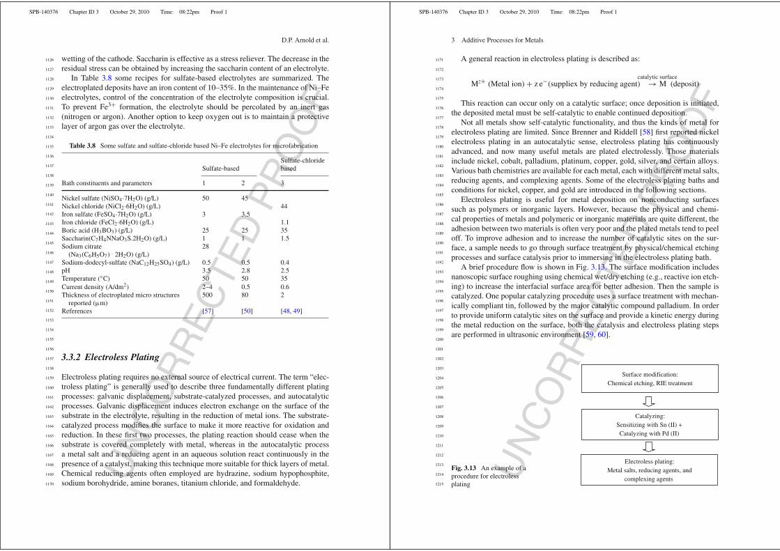
A general reaction in electroless plating is described as:
Mz+ (Metal ion) + z e−(suppliex by reducing agent)catalytic surface
→ M (deposit)
This reaction can occur only on a catalytic surface; once deposition is initiated,the deposited metal must be self-catalytic to enable continued deposition.
Not all metals show self-catalytic functionality, and thus the kinds of metal forelectroless plating are limited. Since Brenner and Riddell [58] first reported nickelelectroless plating in an autocatalytic sense, electroless plating has continuouslyadvanced, and now many useful metals are plated electrolessly. Those materialsinclude nickel, cobalt, palladium, platinum, copper, gold, silver, and certain alloys.Various bath chemistries are available for each metal, each with different metal salts,reducing agents, and complexing agents. Some of the electroless plating baths andconditions for nickel, copper, and gold are introduced in the following sections.
Electroless plating is useful for metal deposition on nonconducting surfacessuch as polymers or inorganic layers. However, because the physical and chemi-cal properties of metals and polymeric or inorganic materials are quite different, theadhesion between two materials is often very poor and the plated metals tend to peeloff. To improve adhesion and to increase the number of catalytic sites on the sur-face, a sample needs to go through surface treatment by physical/chemical etchingprocesses and surface catalysis prior to immersing in the electroless plating bath.
A brief procedure flow is shown in Fig. 3.13. The surface modification includesnanoscopic surface roughing using chemical wet/dry etching (e.g., reactive ion etch-ing) to increase the interfacial surface area for better adhesion. Then the sample iscatalyzed. One popular catalyzing procedure uses a surface treatment with mechan-ically compliant tin, followed by the major catalytic compound palladium. In orderto provide uniform catalytic sites on the surface and provide a kinetic energy duringthe metal reduction on the surface, both the catalysis and electroless plating stepsare performed in ultrasonic environment [59, 60].
Surface modification:
Chemical etching, RIE treatment
Catalyzing:
Sensitizing with Sn (II) +
Catalyzing with Pd (II)
Electroless plating:
Metal salts, reducing agents, and
complexing agents
Fig. 3.13 An example of aprocedure for electrolessplating

UN
CO
RR
EC
TE
D P
RO
OF
SPB-140376 Chapter ID 3 October 29, 2010 Time: 08:22pm Proof 1
1216
1217
1218
1219
1220
1221
1222
1223
1224
1225
1226
1227
1228
1229
1230
1231
1232
1233
1234
1235
1236
1237
1238
1239
1240
1241
1242
1243
1244
1245
1246
1247
1248
1249
1250
1251
1252
1253
1254
1255
1256
1257
1258
1259
1260
D.P. Arnold et al.
3.3.2.1 Nickel
Electroless nickel plating is one of the most popular catalytic electroless processesin use today. It is commonly used in engineering coating applications for wear resis-tance, hardness, and corrosion protection. It is also used in the electronics industryon PCBs as a coating with an overlay of gold to prevent corrosion. The concept andbasic composition has not changed much since the inception of the process [58]. Theelectroless nickel plating bath consists of a source of nickel ions (salts), a reducingagent, complexing agents, and some additives.
Although many nickel salts such as nickel sulfate, nickel chloride, and nickelacetate are available, nickel sulfate is preferred because of its low corrosivenessand low cost. To enhance chemical reduction of nickel at the cathode, a reducingagent is used such as sodium hypophosphite (NaH2PO2 H2O), sodium borohydride(NaBH4), and dimethylamine borane (DMAB). Complexing agents are used forexerting a buffering action to prevent the pH change, preventing the precipitationof nickel salts, and enhancing stable metal reduction. Note that because there areseveral agents inserted in the bath, nickel from electroless plating is not usuallypure but contains other components such as phosphorus or boron.
Table 3.9 shows some bath compositions for electroless nickel deposition withhypophosphite reducing agent (columns 1–4), borohydride reducing agent (columns5–6), and dimethylamine borane reducing agent (columns 7–8) [61].
A step-by-step procedure for nickel electroless plating with a hypophosphitereducing agent is given below [9, 62], which essentially follows the recipe ofTable 3.9 (column 1) except for the amount of hydroxyacetic acid of 30.9 g/L and theprocess temperature of 65◦C. With this recipe, a deposition rate of approximately70 nm/min (4.2 µm/h) is obtained on a printed circuit board and a Si substrate. Theequipment necessary for electroless nickel plating is shown in Fig. 3.14, consistingof an Sn sensitizing bath, a Pd activation bath, an electroless nickel bath, and anultrasonic bath.
Bath Preparation
1. Mix 10 g of SnCl2 and 10 g of HCl. Take 0.375 mL of the solution and mix itwith 120 mL of deionized water to prepare the Sn(II) solution.
2. Mix 10 g of Pd and 10 g of HCl. Take 0.5 mL of the solution and mix it with 100mL of deionized water to prepare the Pd(II) solution.
3. Measure 129.62 g NiCl2, 105.97 g NaH2PO2·H2O, and 61.8 g HOCH2COOHinto a 1 L beaker. Fill the beaker with deionized water to 1 L. Mix using a motor-ized mechanical propeller for at least 2 h. (Note that a magnetic stirring bar is notrecommended because the bath contains ferromagnetic Ni.) This stock solutioncan be stored for a month or two without noticeable degradation.
4. Add NH4OH to obtain a pH level of 4–6. Mix well for 2 h in a similar way to thatdescribed above. This pH adjustment should be performed immediately beforeperforming electroless plating. UN
CO
RR
EC
TE
D P
RO
OF
SPB-140376 Chapter ID 3 October 29, 2010 Time: 08:22pm Proof 1
1261
1262
1263
1264
1265
1266
1267
1268
1269
1270
1271
1272
1273
1274
1275
1276
1277
1278
1279
1280
1281
1282
1283
1284
1285
1286
1287
1288
1289
1290
1291
1292
1293
1294
1295
1296
1297
1298
1299
1300
1301
1302
1303
1304
1305
3 Additive Processes for Metals
Tab
le3.9
Exa
mpl
eba
ths
for
elec
trol
ess
nick
elde
posi
tion
usin
gva
riou
shy
poph
osph
ite
redu
cing
agen
ts
Hyp
opho
sphi
tere
duci
ngag
ent
Bor
ohyd
ride
redu
cing
agen
tD
imet
hyla
min
ebo
rane
redu
cing
agen
t
Bat
hco
nsti
tuen
tsan
dpa
ram
eter
s1
23
45
67
8
Nic
kelc
hlor
ide
(NiC
l 2·6
H2O
)(g
/L)
3030
3020
2417
0N
icke
lsul
fate
(NiS
O4·6
H2O
)(g
/L)
2530
Sod
ium
hypo
phos
phit
e(N
aH2P
O2·H
2O
)(g
/L)
1010
1025
Hyd
roxy
acet
icac
id(H
OC
H2C
OO
H)
(g/L
)35
Sod
ium
citr
ate
(Na 3
C6H
5O
7·2
H2O
)(g
/L)
12.6
84S
odiu
mac
etat
e(N
aC2H
3O
2)
(g/L
)5
Sod
ium
boro
hydr
ide
(NaB
H4)
(g/L
)0.
670.
4E
thyl
ened
iam
ine
(C2H
4(N
H2) 2
)(g
/L)
44S
odiu
mhy
drox
ide
(NaO
H)
(g/L
)40
Am
mon
ium
hydr
oxid
e(N
H4O
H,2
8%N
H3)
(mL
/L)
120
Dim
ethy
lam
ine
bora
ne((
CH
3) 2
NH
BH
3)
(g/L
)37
3.5
Mal
onic
acid
(C3H
2O
4N
a 2,d
isod
ium
salt
)(g
/L)
34A
mm
oniu
mch
lori
de(N
H4C
l)(g
/L)
50B
oric
acid
(H3B
O)
(g/L
)25
Sod
ium
pyro
phos
phat
e(N
a 4P
2O
7·1
0H2O
)(g
/L)
50B
ase
for
neut
rali
zing
NaO
HN
aOH
NH
4O
HN
H4O
HN
aOH
NH
4O
HN
aOH
NH
4O
HpH
4–6
4–6
8–10
10–1
111
114.
255.
5Te
mpe
ratu
re(◦
C)
90–1
0090
–100
9570
9760
1877
Dep
osit
ion
rate
(µm
/h)
157
6.5
158.
81.
32.
321
Ref
eren
ces
[ 62]
[63]
[58]
[64]
[65]
[65]
[66]
[67]

UN
CO
RR
EC
TE
D P
RO
OF
SPB-140376 Chapter ID 3 October 29, 2010 Time: 08:22pm Proof 1
1306
1307
1308
1309
1310
1311
1312
1313
1314
1315
1316
1317
1318
1319
1320
1321
1322
1323
1324
1325
1326
1327
1328
1329
1330
1331
1332
1333
1334
1335
1336
1337
1338
1339
1340
1341
1342
1343
1344
1345
1346
1347
1348
1349
1350
D.P. Arnold et al.
Fig. 3.14 Preparation ofelectroless nickel plating
Thisfigurewill beprintedin b/w
Electroless Nickel Plating Procedure
1. Rinse a substrate in acetone, then methanol, then deionized water, and thensensitize it in the Sn(II) solution for 2 min.
2. Rinse the sample in deionized water for 30 s.3. Catalyze the sample in the prepared Pd(II) solution for 2 min.4. Rinse the sample in deionized water for 30 s.5. Submerge the sample in the prepared electroplating bath at 65◦C in an ultrasonic
environment.
Table 3.10 Ingredients of electroless nickel bath with hypophosphite reducing agent [9]
Bath constituents and parameters Molarity (mol)Molecularweight Mass (g/L)
AQ2
Nickel chloride(NiCl2·6H2O)
0.23 129.62 30
Sodium hypophosphate(NaH2PO2·H2O)
0.09 105.97 10
Hydroxyacetic acid(HOCH2COOH)
0.5 61.8 30.90
pH 4–6 (using NH4OH or NaOH for adjustment)Temperature 65◦C
3.3.2.2 Copper
Some electroless copper plating recipes use formaldehyde or its derivatives as areducing agent. However, such plating baths produce toxic formaldehyde vapor dur-ing the process and require high pH (~12.5). An alternative bath uses hypophosphiteas the reducing agent. Table 3.11 shows some bath compositions for electroless cop-per deposition with formaldehyde reducing agent (columns 1–3) and hypophosphitereducing agent (column 4) [61, 68]. U
NC
OR
RE
CTE
D P
RO
OF
SPB-140376 Chapter ID 3 October 29, 2010 Time: 08:22pm Proof 1
1351
1352
1353
1354
1355
1356
1357
1358
1359
1360
1361
1362
1363
1364
1365
1366
1367
1368
1369
1370
1371
1372
1373
1374
1375
1376
1377
1378
1379
1380
1381
1382
1383
1384
1385
1386
1387
1388
1389
1390
1391
1392
1393
1394
1395
3 Additive Processes for Metals
Table 3.11 Example baths for electroless copper deposition using formaldehyde reducing agentand hypophosphite reducing agent
Formaldehyde reducingagent
Hypophosphitereducing agent
Bath constituents and parameters 1 2 3 4
Copper sulfate (CuSO4·5H2O) (g/L) 3.6 30 10 3.83Nickel sulfate (NiSO4·6H2O) (g/L) 0.53Boric acid (H3BO3) (g/L) 30.9Sodium hypophosphite (NaH2PO2·H2O) (g/L) 28.6Sodium potassium tartrate (KNaC4H4O6·4H2O)
(g/L)25 99
Sodium hydroxide (NaOH) (g/L) 3.8 50 10Sodium carbonate (Na2CO3) (g/L) 32Formaldehyde (HCOOH (37%)) (g/L) 10 29 20.3Sodium citrate (Na3C6H5O7·2H2O) (g/L) 15.3Methyldichlorosilane (CH3Cl2SiH) (g/L) 0.25Ethylenediaminetetraacetic acid (EDTA)
tetrasodium (N,N′-1,2-Ethanediylbis[N-(carboxymethyl)glycene]tetrasodium) (g/L)
20
Temperature (◦C) 22 25 63 65Deposition rate (µm/h) 0.5 2.5 6.3 8.5References [69] [70] [71] [68]
The hypophosphite reduced electroless copper plating has advantages includingbath stability, no toxic gas generation, and operation in a lower pH environment.However, because the deposited copper cannot catalyze the oxidation of hypophos-phite, the bath needs a small amount of nickel for continuous plating and boric acidfor a high plating rate, resulting in impure copper deposition.
A step-by-step procedure for copper electroless plating with a hypophosphitereducing agent [68] is given below as an example.
Bath Preparation
1. Mix 10 g of SnCl2 and 10 g of HCl. Take 0.375 mL of the solution and mix itwith 120 mL of deionized water to prepare the Sn(II) solution.
2. Mix 10 g of Pd and 10 g of HCl. Take 0.5 mL of the solution and mix it with 100mL of deionized water to prepare the Pd(II) solution.
3. Mix the electroless copper plating bath with hypophosphite reducing agentfollowing Table 3.11 (column 4).
4. Adjust the pH with either KOH or NaOH pellets to the desired pH level (Here itis 9–9.5).
Note that all ingredients are mixed and dissolved in water together. The mixtureafter step 3 can have a shelf life of about a month, but the mixture after step 4 tends
UN
CO
RR
EC
TE
D P
RO
OF
SPB-140376 Chapter ID 3 October 29, 2010 Time: 08:22pm Proof 1
1396
1397
1398
1399
1400
1401
1402
1403
1404
1405
1406
1407
1408
1409
1410
1411
1412
1413
1414
1415
1416
1417
1418
1419
1420
1421
1422
1423
1424
1425
1426
1427
1428
1429
1430
1431
1432
1433
1434
1435
1436
1437
1438
1439
1440
D.P. Arnold et al.
to plate a thin copper layer on the container wall in a few days. The pH adjustmentshould be done right before electroless plating is performed. The solution shouldhave a clean blue color.
Electroless Copper Plating Procedure
1. Rinse substrate in acetone, then methanol, and then deionized water, and thensensitize it in the prepared Sn(II) solution for 2 min.
2. Rinse the substrate in deionized water for 30 s.3. Catalyze the substrate in the prepared Pd(II) solution for 2 min.4. Rinse the substrate in deionized water for 30 s.5. Submerge the substrate in the prepared electroless plating bath.
3.3.2.3 Gold
Because of its high chemical stability and mechanical ductility, gold becomes anindispensable material in the electronics industry. Despite its importance, electro-less gold plating [29] has been underdeveloped compared with electroless nickel orcopper. Useful electroless gold plating using borohydride or amine borane as thereducing agent has been reported [72, 73]. A typical bath composition is shown inTable 3.12.
Table 3.12 Ingredients of electroless gold bath with borohydride reducing agent [73]
Bath constituents and parameters Molarity (mol) Molecular weight Mass (g/L)
Potassium gold cyanide(KAu(CN)2)
0.02 290 5.8
Potassium cyanide (KCN) 0.2 65 13Potassium hydroxide (KOH) 0.2 56 11.2Potassium borohydride (KBH4) 0.4 54 21.6Temperature 75◦CDeposition rate 0.7–3.5 µm/h (with stirring)
Bath Preparation (2.5× Concentration) [67]
1. Dissolve 28 g KOH and 32.5 g KCN in about 500 mL of deionized water.2. Add 54 g KBH4 and stir until dissolution.3. Dissolve 14.4 g KAu(CN)2 in about 250 mL deionized water.4. Mix the above two solutions, and dilute to 1 L.5. Filter through Whatman 41 filter paper or equivalent.6. Dilute 1 volume of this solution with 1.5 volumes of deionized water to make a
2.5× bath. UN
CO
RR
EC
TE
D P
RO
OF
SPB-140376 Chapter ID 3 October 29, 2010 Time: 08:22pm Proof 1
1441
1442
1443
1444
1445
1446
1447
1448
1449
1450
1451
1452
1453
1454
1455
1456
1457
1458
1459
1460
1461
1462
1463
1464
1465
1466
1467
1468
1469
1470
1471
1472
1473
1474
1475
1476
1477
1478
1479
1480
1481
1482
1483
1484
1485
3 Additive Processes for Metals
3.3.3 Comparison of Electroplating and Electroless Plating
Ni, Cu, and Au microstructures can all be fabricated by electroplating or electro-less plating. Compared to electroplating, electroless plating contains the followingcharacteristics and advantages [61].
1. No power supply and electrical contact is necessary.2. Deposition may occur on a nonconducting surface.3. More uniform deposition can be formed on three-dimensional geometry without
electric field influence.4. Deposits are often less porous.
There are disadvantages of electroless plating too. Often the electroless bathsrequire higher temperatures and have a relatively short lifetime. Electroless platingis also prone to poor adhesion. Care should be taken when storing electroless platingbaths. A container made of plastic or glass is often found to be covered with elec-troless plated metal after being stored on the shelf for a while. Also, for electrolessplating, the deposition rate is relatively slow, and metal layers thicker than a fewmicrometers are not recommended. In addition, electroless plating metal in selectedregions can sometimes be quite challenging. For example, selective deposition ona metal surface is fairly easy, but selective coating a polymer on SiO2 is not veryeffective (the bath will likely deposit on both the polymer and SiO2 surfaces).
Costs of electroplating and electroless plating are fairly similar. The electrolessplating process requires a chemical reducing agent for metal ions to be convertedinto the elemental conformation, therefore it is considered as a more expensive pro-cess from the material cost point of view. However, this chemical cost is offset by theadvantage of not requiring equipment such as power supplies or switching circuitsfor advanced current control.
There are clearly pros and cons associated with both electroplating and electro-less plating. In situations where either electroplating or electroless plating couldtheoretically be used, the decision for one or the other is often dependent on manyprocess integration issues. In general, electroless plating can be considered as acomplement to electroplating rather than a “competitor.”
3.4 LIGA and UV-LIGA Processes
One of the most distinctive MEMS processes is the construction of thick and high-aspect-ratio three-dimensional (3-D) microstructures. High aspect ratio is modestlydefined as a height to width ratio of 2 to 1 or greater. Fabrication of these structuresoften relies on X-ray or UV lithography of thick polymer layers.4 The patterned
4See Chapter 9 for more information on lithography.

UN
CO
RR
EC
TE
D P
RO
OF
SPB-140376 Chapter ID 3 October 29, 2010 Time: 08:22pm Proof 1
1486
1487
1488
1489
1490
1491
1492
1493
1494
1495
1496
1497
1498
1499
1500
1501
1502
1503
1504
1505
1506
1507
1508
1509
1510
1511
1512
1513
1514
1515
1516
1517
1518
1519
1520
1521
1522
1523
1524
1525
1526
1527
1528
1529
1530
D.P. Arnold et al.
polymeric structures can be used directly as a MEMS device or used as a mold formetal electrodeposition. In this section, two fabrication approaches for achievinghigh-aspect-ratio 3-D electroformed metallic structures are described: one with X-ray lithography (LIGA), and the other with UV lithography (UV-LIGA or LIGA-Like).5
3.4.1 Process Explanation
Both LIGA and UV-LIGA processes share common fabrication steps except for theinitial step of polymeric mold fabrication. A general fabrication procedure for bothprocesses is described in this section.
Because these are surface micromachining processes, there is no strict crite-rion for substrate selection. A variety of substrates such as Si, glass, ceramic, andprinted wiring board are available, however, an oxidized Si substrate is used as anexample here (Fig. 3.15). An electrical seed layer typically consisting of Ti/Cu orCr/Cu is deposited on the substrate using either sputtering or evaporation. Cu does
Deposit thin
adhesion/seed
layers
Begin with
oxidized Si
substrate
Photodefine
polymer
mask/ mold
Electroplate
metal
Etch polymer
mold and thin
metal layers
Fig. 3.15 Basicelectroplating process to formsingle-layer metal structures
5The German acronym “LIGA” refers to a three-step process: X-ray-Lithography, Electroplating(german: Galvanik), Polymer Replication (German: Abformung). Nowadays, “LIGA” is commonlyused in reference to the two-step process of lithography and electroplating (excluding the polymerreplication step). U
NC
OR
RE
CTE
D P
RO
OF
SPB-140376 Chapter ID 3 October 29, 2010 Time: 08:22pm Proof 1
1531
1532
1533
1534
1535
1536
1537
1538
1539
1540
1541
1542
1543
1544
1545
1546
1547
1548
1549
1550
1551
1552
1553
1554
1555
1556
1557
1558
1559
1560
1561
1562
1563
1564
1565
1566
1567
1568
1569
1570
1571
1572
1573
1574
1575
3 Additive Processes for Metals
not stick well to most substrates so Ti or Cr is employed as an adhesion layer(see Section 3.5.1). Typical thicknesses of Ti (or Cr) and Cu are 10–30 nm and100–300 nm, respectively. After the seed layer deposition, a thick polymer layeris coated, soft-baked, and lithographically patterned to form a micromold for asubsequent electroplating. LIGA typically uses polymethylmethacrylate (PMMA)or SU-8 (an epoxy-based polymer) for X-ray lithography, whereas UV-LIGA usesvarious UV-sensitive photoresists including DNQ-novolak-based photoresist, SU-8,polyimide, and others.
With the photoresist mold in place, the substrate is then electroplated. The elec-troplated metal fills the mold confined by the sidewalls. Usually the electroplatingis stopped before it reaches the top of the mold. But sometimes it is electroplatedover the mold to form “mushroom”-type structures for some applications. Afterelectroplating, the polymer mold is removed using a solvent and/or plasma etching.The electroplated structures are still electrically connected to each other through theseed layer. The Cu and Ti seed layers are then sequentially time etched to isolate theelectroplated structures electrically and complete the process.
With the introduction in the 1990s of UV photopatternable high-aspect-ratiopolymers such as SU-8, high-quality sidewall and high-aspect-ratio molds couldbe fabricated using UV lithography, as compared to X-ray lithography. The electro-forming process using UV-patterned molds and subsequent electroplating has beencalled UV-LIGA, LIGA-like, or often “poor man’s LIGA.”
The UV-LIGA process does not provide the extreme aspect ratios possible withX-ray LIGA, but is sufficiently suitable for many applications. A good guidelineis that an aspect ratio of 6:1 can be fabricated by UV-LIGA. It is also restrictedto a maximum resist height of 800 µm or so. Also submicron pattern dimensionsmay not be effectively produced because of the wavelength of the UV source, forexample, i-line (λ = 365 nm). However, in addition to low cost in equipment, theprocess has other advantages such as batch processability, manufacturability, andrelative simplicity, providing an affordable system set for laboratory and industrialusage.
3.4.2 Electroplating in LIGA and UV-LIGA Microstructures
The height and surface profile of high-aspect-ratio electrodeposited metal structuresand the homogeneity of their thickness distribution are influenced by various factors,which can interfere with each other. The main factors and important effects areexplained in this section.
The deposition rate is proportional to the current density. Therefore a higher cur-rent density results in a thicker deposit. The distribution of the current density isassociated with the distribution of the electric field lines (primary current distribu-tion). Because the metal surface is highly conductive, the field lines are normal tothe electrode surface. If the anode has a larger area than the cathode, the field linedensity and current density are higher at the edge of the substrate, which causes a

UN
CO
RR
EC
TE
D P
RO
OF
SPB-140376 Chapter ID 3 October 29, 2010 Time: 08:22pm Proof 1
1576
1577
1578
1579
1580
1581
1582
1583
1584
1585
1586
1587
1588
1589
1590
1591
1592
1593
1594
1595
1596
1597
1598
1599
1600
1601
1602
1603
1604
1605
1606
1607
1608
1609
1610
1611
1612
1613
1614
1615
1616
1617
1618
1619
1620
D.P. Arnold et al.
thicker deposit at the edge of the substrate (“macro bathtub effect”). If the cathodesurface is patterned with resist structures, the electric field lines bend, and a currentconcentration occurs at the edge of the structures [74, 75]. Therefore the electro-plated layer is usually thicker near the edges of the electroplated features (“microbathtub effect”) and sometimes higher in narrow structures than in wide structures,as shown in Fig. 3.16.
Another consideration for electroplating in high-aspect-ratio features is that thetransport mechanism of the metal ions depends on feature size and depth. As aresult, the electroplating rate may vary during the plating process [76]. Figure 3.17shows three different states that occur in filling a mold structure by electroplating.At the beginning of the deposition, the process is highly diffusion limited. As theplated layer grows and the trenches begin to fill, the diffusion limitations begin towane. At an intermediate filling, the penetration range of the convection is reached.This depends on the lateral size of the structure itself. In the case of structures withsufficiently wide lateral dimensions, the flow velocity in the plating bath reduces theextension of the diffusion layer, as described in Section 3.3.1.2. Very high-aspect-ratio structures therefore show a reduced plating rate in the beginning of plating. Inthis case, the electroplated layer would be thinner in narrow structures, as comparedto wider structures.
Fig. 3.16 Schematic of electrical field line distribution using resist-patterned substrates. The fieldline density is higher within narrow structures and at the edge of wide structures, which affects theheight and surface profile of the electroplated microstructures
Fig. 3.17 Schematic of the diminishing influence of diffusion during metal growth. The diffusionlayer thickness depends on process progress and on the penetration range of convection. At t 3, thedeposition rate is improved due to spherical diffusion
Thisfigurewill beprintedin b/w
UN
CO
RR
EC
TE
D P
RO
OF
SPB-140376 Chapter ID 3 October 29, 2010 Time: 08:22pm Proof 1
1621
1622
1623
1624
1625
1626
1627
1628
1629
1630
1631
1632
1633
1634
1635
1636
1637
1638
1639
1640
1641
1642
1643
1644
1645
1646
1647
1648
1649
1650
1651
1652
1653
1654
1655
1656
1657
1658
1659
1660
1661
1662
1663
1664
1665
3 Additive Processes for Metals
All these effects cause inhomogeneous deposition rates over the substrate as wellas within the features. To minimize these unwanted effects and improve the platinguniformity, some rules are given in the following.
1) Use a shield or a wafer holder to homogenize the electrical field at themacroscopic scale.
2) Use dummy plating areas over the whole substrate to promote a homogenouscurrent distribution.
3) Use microstructured dummy areas that surround the functional features.4) Use moderate flow to get similar heights of diffusion layers.5) Use moderate current density to avoid insufficient supply of ions at the bottom
of the microstructure.6) Limit the deposition height to be about 2/3 of the mold height (see Fig. 3.17
for t2).
More rules for LIGA design can be found in [77].To show the potential of the LIGA techniques, one example is given. Figure 3.18
shows (a) a SU-8 resist mold and (b) the replicated Ni–Fe structure. The electroplat-ing produces the exact negative of the structural details and the sidewall roughnessof the resist mold. In Fig. 3.19 a commercially available micro gear system isshown. Crucial features for this application are the high aspect ratio in combina-tion with the parallel sidewalls of the resist structure, which is typical for LIGA.Other applications of LIGA are described in [78, 79].
3.4.3 Multilevel Metal Structures
Often multiple metal levels and vias are necessary to enable complex wiring inter-connections or complex mechanical microstructures. Multilevel fabrication can beachieved by extending the previously described process (see Section 3.4.1) usingmultiple masking and electroplating steps. For wire connections, an interlayerdielectric material must be selected to electrically insulate the metal layers fromeach other to avoid unexpected short circuits. Considering that the top surface ofthe first metal layer may be fairly rough (typical of many electroplated metals), thedielectric must be able to conformally and completely coat the top and side surfacesof the lower metal layer. Even the smallest pinhole defect in the interlayer dielec-tric can cause the electrical insulation to fail. Commonly used interlayer dielectricmaterials include PECVD or sputtered oxide/nitride, spin-on glass, or a chemicallystable spin-coated polymer such as polyimide or SU-8. The intended temperature ofoperation must also be considered, because polymer dielectrics may not be suitableat a 100◦C or more.
A fabrication process for achieving a two-layer metal structure is shown inFig. 3.20. The process begins by depositing the first metal layer as described inFig. 3.15. The interlayer dielectric is deposited and vias are opened to provide

UN
CO
RR
EC
TE
D P
RO
OF
SPB-140376 Chapter ID 3 October 29, 2010 Time: 08:22pm Proof 1
1666
1667
1668
1669
1670
1671
1672
1673
1674
1675
1676
1677
1678
1679
1680
1681
1682
1683
1684
1685
1686
1687
1688
1689
1690
1691
1692
1693
1694
1695
1696
1697
1698
1699
1700
1701
1702
1703
1704
1705
1706
1707
1708
1709
1710
D.P. Arnold et al.
(a)
(b)
Fig. 3.18 SEM micrographof high-aspect-ratiomicrostructures: (a) SU-8resist mold; (b) electroplatedNi–Fe [57] (Reprinted withpermission. Copyright 2008Springer Europe)
interconnects between the two metal layers. For many films, this step requiresthe patterning of a photoresist mask and a subsequent etch. In contrast, the useof a photosensitive polymer dielectric offers the opportunity for simple one-stepphotodefinition.
After the interlayer dielectric is formed, a new adhesion/seed layer is required,because a conductive electrical surface is needed for electroplating. In order to pro-vide sufficient step-coverage over the topography created by the first metal layer,sputtering is the preferred method. It should be noted that adhesion of the metal toa polymer interlayer dielectric can be quite low. If necessary, adhesion promotersmay be used to improve adhesion of the metal (see Section 3.5.1).
After the seed layer deposition, a polymer mold is photodefined to create thepattern for the second metal layer, and the metal is subsequently electrodeposited tothe desired thickness. Afterwards, the polymer mold and thin metal layers are etchedaway. If necessary a passivation layer can be deposited on top of the second metallayer for protection from the environment. Also with the right selection of materials, U
NC
OR
RE
CTE
D P
RO
OF
SPB-140376 Chapter ID 3 October 29, 2010 Time: 08:22pm Proof 1
1711
1712
1713
1714
1715
1716
1717
1718
1719
1720
1721
1722
1723
1724
1725
1726
1727
1728
1729
1730
1731
1732
1733
1734
1735
1736
1737
1738
1739
1740
1741
1742
1743
1744
1745
1746
1747
1748
1749
1750
1751
1752
1753
1754
1755
3 Additive Processes for Metals
Fig. 3.19 Ni–Fe microplanetary gear system; structure height = axial length : 1 mm, diameter8 mm (Reprinted with Permission. Copyright 2009 Micromotion GmbH, Germany)
the interlayer dielectric can be selectively etched away to create “free-standing”bridge segments that are isolated by air [80–82].
In addition to the planar metal layers, some MEMS devices creatively employhigh-aspect-ratio vertical via structures for mechanical or electrical functionality.For example, metal vias are used for vertical interconnects in MEMS packag-ing applications [83] and for electrical passive components in RF MEMS [84].Fabrication of vias with high aspect ratios is often desired, and various methodsfor achieving such structures are shown in Fig. 3.21.
The different characteristics of these approaches are summarized in Table 3.13and described as follows. First is the damascene process, used extensively in siliconVLSI processing [85]. In damascene, an oxide mold is used, and conformal seedlayers are sputtered, followed by copper electrodeposition. Excess copper protrud-ing from the molds is removed by chemical mechanical polishing (CMP),6 leavingcopper only in the via or trench. The interdielectric oxide layers bounding the cop-per are intended to remain at the end of the process, serving as an electrical insulatorand mechanical supporting layer for the subsequent processes.
For 3-D polymeric-mold-based processes such as LIGA or UV-LIGA, CMP maydamage the softer polymer mold material resulting in uneven surface morphology.To avoid polishing steps, several alternatives have been explored. The plate-through-mold approach uses seed layers deposited before the molds. The plating time isproportional to the depth of the mold, and the mold often must be removed afterthe plating, which lengthens the process time further. Moreover, removal of somepolymeric molds such as polyimide or SU-8 often relies on expensive (and relativelyslow) dry etching processes.
6See Chapter 13 (specifically Section 13.7) for more information on CMP.

UN
CO
RR
EC
TE
D P
RO
OF
SPB-140376 Chapter ID 3 October 29, 2010 Time: 08:22pm Proof 1
1756
1757
1758
1759
1760
1761
1762
1763
1764
1765
1766
1767
1768
1769
1770
1771
1772
1773
1774
1775
1776
1777
1778
1779
1780
1781
1782
1783
1784
1785
1786
1787
1788
1789
1790
1791
1792
1793
1794
1795
1796
1797
1798
1799
1800
D.P. Arnold et al.
ElectroplateMetal 1 layer
Deposit inter-layer dielectricand pattern vias
Sputter thinadhesion/seedlayers
Photodefinepolymer mold for Metal 2
ElectroplateMetal 2 layer
Etch polymermold and thinmetal layers
Fig. 3.20 Electroplating process to form multilayer conductive layers
Another approach – a wet etch back process – has also been used for high-aspect-ratio via connections with polymer molds [86]. This process is similar to damascene,except that a wet chemical etch is used to etch back protruding copper, as opposedto CMP. Although suitable for polymer molds, planarity is problematic.
An embedded conductor fabrication (as previously described in Fig. 3.20) usesmold formation and a combination of two simultaneous plating processes: a con-formal plating process through nonremovable lower via mold and a conventional U
NC
OR
RE
CTE
D P
RO
OF
SPB-140376 Chapter ID 3 October 29, 2010 Time: 08:22pm Proof 1
1801
1802
1803
1804
1805
1806
1807
1808
1809
1810
1811
1812
1813
1814
1815
1816
1817
1818
1819
1820
1821
1822
1823
1824
1825
1826
1827
1828
1829
1830
1831
1832
1833
1834
1835
1836
1837
1838
1839
1840
1841
1842
1843
1844
1845
3 Additive Processes for Metals
(a) (b) (c) (d)
1. Oxide mold 1. Seed layer 1. SU-8 mold 1. SU-8 mold
2. Conformal seed layer 2. PR mold 2. Conformal seed layer 2. Conformal seed
layer
3. Conformal
electroplating
3. Conformal
electroplating
3. Plate-through-mold 3. PR patterning for
upper layer
4. Polishing(CMP) 4. Repeat 1–3 4. Wet etching 4. Conformal+
plate-through-mold
1oxide
2seed layer
3
4
5
1
2PR
3
4
5
1SU-8
2seed layer
3
4
5
1
2seed layer
3
4
5
SU-8
PR
5. Repeat 1–4 5. Remove PR and
seed layer
5. Follow (b) 3–5 5. Remove PR and
seed layer
Fig. 3.21 Fabrication process comparison for one via and one upper conducting layer configura-tion: (a) damascene process; (b) conventional plate-through-mold process; (c) conformal platingprocess with etch back; (d) conformal plating without etch back [84] (Reprinted with permission.Copyright 2005 IOP)
Thisfigurewill beprintedin b/w
plate-through-mold process through a removable upper conductor mold [84]. Thevias are embedded in the mold from which they are formed: the mold is not removedafter the structures are completed. This eliminates a long etching step for the moldremoval, which simplifies and shortens the process. Also, the conformal platingmakes the via fill time independent of the via height. At the end of the process,the conductors are embedded in the mold, resulting in good mechanical strength forsubsequent process or packaging steps. The low-temperature polymeric process alsofacilitates post-CMOS compatibility if necessary.

UN
CO
RR
EC
TE
D P
RO
OF
SPB-140376 Chapter ID 3 October 29, 2010 Time: 08:22pm Proof 1
1846
1847
1848
1849
1850
1851
1852
1853
1854
1855
1856
1857
1858
1859
1860
1861
1862
1863
1864
1865
1866
1867
1868
1869
1870
1871
1872
1873
1874
1875
1876
1877
1878
1879
1880
1881
1882
1883
1884
1885
1886
1887
1888
1889
1890
D.P. Arnold et al.
Tab
le3.1
3V
ario
uspr
oces
ses
for
mul
tila
yer
cond
ucto
rla
yers
wit
hvi
as[8
4]
Dam
asce
neC
onve
ntio
nal
plat
e-th
roug
h-m
old
proc
ess
Con
form
alpl
atin
gpr
oces
sw
ith
etch
back
Con
form
alpl
atin
gpr
oces
sw
itho
utet
chba
ck
Mol
dm
ater
ial
Oxi
de(c
eram
ic)
Pol
ymer
(org
anic
)P
olym
er(o
rgan
ic)
Pol
ymer
(org
anic
)M
old
rem
oval
No
Yes
No
No
Met
alde
posi
tion
tim
eS
hort
Lon
gS
hort
Sho
rtN
umbe
rof
plat
ing
per
two
laye
rs2
22
1
Exc
ess
met
alre
mov
alP
olis
hing
(CM
P)
No
Che
mic
alet
chin
gN
oM
old
eros
ion
orm
etal
dish
ing
Sus
cept
ible
duri
ngC
MP
N/A
Met
aldi
shin
gdu
ring
etch
-bac
kN
/A
Met
also
urce
usag
eN
onec
onom
ical
Eco
nom
ical
Non
econ
omic
alE
cono
mic
alD
evic
epa
ckag
ing
Inje
ctio
nm
oldi
ngP
olym
eror
cavi
typa
ckag
ing
Inje
ctio
nm
oldi
ngIn
ject
ion
mol
ding
App
lica
tion
sIC
inte
rcon
nect
ME
MS
actu
ator
,RF
pass
ives
,int
erco
nnec
t,po
wer
devi
ces
ME
MS
inte
rcon
nect
,RF
pass
ives
,pow
erde
vice
sM
EM
Sin
terc
onne
ct,R
Fpa
ssiv
es,p
ower
devi
ces
Ref
eren
ces
[85]
[80]
[86]
[84]
Rep
rint
edw
ith
perm
issi
on.C
opyr
ight
2005
IOP
UN
CO
RR
EC
TE
D P
RO
OF
SPB-140376 Chapter ID 3 October 29, 2010 Time: 08:22pm Proof 1
1891
1892
1893
1894
1895
1896
1897
1898
1899
1900
1901
1902
1903
1904
1905
1906
1907
1908
1909
1910
1911
1912
1913
1914
1915
1916
1917
1918
1919
1920
1921
1922
1923
1924
1925
1926
1927
1928
1929
1930
1931
1932
1933
1934
1935
3 Additive Processes for Metals
3.5 Materials Properties and Process Selection Guidelines
for Metals
This section provides general guidelines for the selection of metals for use inMEMS. It also provides relevant material properties and application issues relatingto adhesion, electrical, mechanical, thermal, and magnetic aspects.
3.5.1 Adhesion
Regardless of the intended functional application, adhesion of any metal to a par-ticular substrate is critical to ensure successful microfabrication and long-termreliability. Adhesion depends on many factors, including type of substrate, rough-ness of the substrate, deposition methods, thickness of the film, and so on. Theadhesion is determined by the interfacial energies of the interface, which may bemetal–metal, metal–dielectric, or metal–polymer. Delamination occurs when theintrinsic and extrinsic stress in the deposited metal films overcomes the interfacialenergy. Generally, cracking is caused by tensile stress, and peeloff by compressivestress.
Intrinsic stress is the result of crystallographic defects in the film, and extrin-sic stress is due to the thermal expansion mismatch between the film and substrate[87]. For most MEMS applications, the extrinsic stress plays a major role. However,intrinsic stress can also be problematic. For example, stress accumulates withincreasingly thick electroplated films, so this stress often limits how thick anelectrodeposited layer may become.
Table 3.14 qualitatively summarizes the adhesion of various metals to differentmaterials. Many metals, especially noble metals, do not adhere very well to commonMEMS substrates such as Si, SiO2, or glass. Often, however, thin layers of interfa-cial materials can be used to improve adhesion. The most widely used adhesionenhancing layers are Ti and Cr (as well as Ta and W) with thickness of 5–20 nm,usually sputtered or evaporated.
The reason for this enhancement is as follows [91]. These adhesion-promotingmetals all readily oxidize, in contrast to noble metals such as Au, Ag, and Pt. Thus,
Table 3.14 Qualitative adhesion of thin film metals to different substrates
Si [87] SiO2 [87] Polyimide [88, 89] PDMS [90]
Al Moderate Good Moderate –Au Moderate Poor Poor PoorCr Good Good Good GoodCu Moderate Poor Poor PoorNi Moderate Good Poor –Pt Moderate Good – PoorTa Good – Good –Ti Good Good Good Good
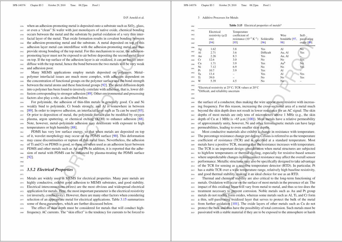
UN
CO
RR
EC
TE
D P
RO
OF
SPB-140376 Chapter ID 3 October 29, 2010 Time: 08:22pm Proof 1
1936
1937
1938
1939
1940
1941
1942
1943
1944
1945
1946
1947
1948
1949
1950
1951
1952
1953
1954
1955
1956
1957
1958
1959
1960
1961
1962
1963
1964
1965
1966
1967
1968
1969
1970
1971
1972
1973
1974
1975
1976
1977
1978
1979
1980
D.P. Arnold et al.
when an adhesion-promoting metal is deposited onto a substrate such as SiO2, glass,or even a “clean” Si wafer with just monolayers of native oxide, chemical bondingoccurs between the metal and the substrate by partial oxidation of a very thin inter-facial layer of the metal. That oxide formation results in covalent bonding betweenthe adhesion-promoting metal and the substrate. A metal deposited on top of thisadhesion layer metal can interdiffuse with the adhesion-promoting metal and thusprovide strong bonding of the top metal. For this mechanism to occur, the adhesion-promoting layer must not be exposed to air before depositing the second metal layeron top. If the top surface of the adhesion layer is air oxidized, it can no longer inter-diffuse with the top metal, hence the bond between the two metals will be very weakand adhesion poor.
Many MEMS applications employ metals deposited on polymers. Metal–polymer interfacial issues are much more complex, with adhesion dependent onthe concentration of functional groups on the polymer surface and the bond strengthbetween the metal atoms and these functional groups [92]. The metal diffusion depthinto a polymer has been found to inversely correlate with adhesion, that is, lower dif-fusion corresponding to stronger adhesion [89]. Other environmental and processingfactors also play a role, as described below.
For polyimide, the adhesion of thin-film metals is generally good. Cu and Niweakly bind to polyimide, Cr bonds strongly, and Al is somewhere in between[89]. In order to improve adhesion, an interfacial layer such as Ta can be used [93].Or prior to deposition of metal, the polyimide surface can be modified by oxygenplasma, argon sputtering, or chemical etching (KOH) to enhance adhesion [88].Note, however, metal–polyimide adhesion may deteriorate with exposure to hightemperatures or high humidity [88].
PDMS has very low surface energy, so that when metals are deposited on topof it, wavelet morphology may occur on the PDMS surface [90]. This deformationmay cause discontinuities or rupture of thin metal lines. Nevertheless, the adhesionof Ti and Cr on PDMS is good, so these are often used as an adhesion layer betweenPDMS and other metals such as Au and Pt. In addition, it is reported that the adhe-sion of metal with PDMS can be enhanced by plasma-treating the PDMS surface[92].
3.5.2 Electrical Properties
Metals are widely used in MEMS for electrical properties. Many pure metals arehighly conductive, exhibit good adhesion to MEMS substrates, and good stability.Electrical interconnections (wires) are the most obvious and widespread electricalapplication for metals. Here, the most important parameter is the electrical resistivity(or inversely, conductivity). However, there are many other factors when consideringselection of an appropriate metal for electrical applications. Table 3.15 summarizessome of these parameters, which are further discussed below.
The effect of skin depth must be considered for metals that will conduct high-frequency AC currents. The “skin effect” is the tendency for currents to be forced to U
NC
OR
RE
CTE
D P
RO
OF
SPB-140376 Chapter ID 3 October 29, 2010 Time: 08:22pm Proof 1
1981
1982
1983
1984
1985
1986
1987
1988
1989
1990
1991
1992
1993
1994
1995
1996
1997
1998
1999
2000
2001
2002
2003
2004
2005
2006
2007
2008
2009
2010
2011
2012
2013
2014
2015
2016
2017
2018
2019
2020
2021
2022
2023
2024
2025
3 Additive Processes for Metals
Table 3.15 Electrical properties of metalsa
Electricalresistivity (µ�
cm)[94]
Temperaturecoefficient ofresistance (10–3 K–1)[95]
Solderable[96]
Wirebondable [97,98]
Self-passivatingoxide [99]
Ag 1.62 3.8 Yes Al NoAl 2.71 3.6 Difficult Au, Al YesAu 2.26 8.3 Yes Au, Al –Cr 12.6 3.0 No No YesCu 1.71 3.9 Yes Aub NoNi 7.12 6.9 No No YesPt 10.7 3.9 Yes Al –Ta 13.4 – Yes Al YesTi 39.0 – No No YesW 5.39 4.5 No No –
aElectrical resistivity at 25◦C; TCR values at 20◦CbDifficult, and reliability uncertain
the surface of a conductor, thus making the wire appear more resistive with increas-ing frequency. For this reason, increasing the cross-sectional area of a metal muchbeyond the skin depth does not result in lower resistance for an AC signal. The skindepths of most metals are only tens of micrometers above 1 MHz (e.g., the skindepth of Cu at 1 MHz is ~65 µm [100]). Most metals have a relative permeabilityof approximately unity, however, Ni and other ferromagnetic metals can have largepermeabilities, leading to even smaller skin depths.
Most conductive materials also exhibit a change in resistance with temperature.The percentage resistance change per degree Celsius is referred to as the temperaturecoefficient of resistance (TCR) and is specified at a standard temperature. Mostmetals have a positive TCR, meaning that the resistance increases with temperature.The TCR is an important design consideration when metal structures are subjectedto high/low temperatures or thermal cycling, especially for resistive-based sensorswhere unpredictable changes in interconnect resistance may affect the overall sensorperformance. Metallic structures may also be specifically designed to take advantageof the TCR for sensing as a resistive temperature detector (RTD). In particular, Pthas a stable TCR over a wide temperature range, relatively high baseline resistivity,and good thermal stability, making it an ideal choice for use as an RTD.
Thermal and chemical stability are also critical to the long-term functioning ofmetals. Oxidation will occur on the surface of most metals in the presence of air. Theimpact of this oxidized layer will vary from metal to metal, and thus so too does thetreatment necessary to prevent corrosion. Noble metals such as Au and Pt groupmetals do not readily form oxides, whereas some metals such as Al, Ti, and Cr forma thin, self-passivating oxidized layer that serves to protect the bulk of the metalfrom further oxidation [101]. The oxide layers of other metals such as Cu do notprotect the bulk and thus have the possibility of total corrosion. Such metals must bepassivated with a stable material if they are to be exposed to the atmosphere or harsh

UN
CO
RR
EC
TE
D P
RO
OF
SPB-140376 Chapter ID 3 October 29, 2010 Time: 08:22pm Proof 1
2026
2027
2028
2029
2030
2031
2032
2033
2034
2035
2036
2037
2038
2039
2040
2041
2042
2043
2044
2045
2046
2047
2048
2049
2050
2051
2052
2053
2054
2055
2056
2057
2058
2059
2060
2061
2062
2063
2064
2065
2066
2067
2068
2069
2070
D.P. Arnold et al.
conditions for long periods of time. Also, when creating contacts to these metals insuccessive metallization steps, the oxide should be removed immediately prior tothe contact being made. Sputtering tools often feature an argon sample sputteringthat can etch away the oxidized layer by ion milling. This is particularly useful, asthe freshly cleaned metal surface is kept in an inert environment until sputtering thenext metal.
Another important design aspect that can be easily overlooked is external connec-tions. Most MEMS devices use bond pads on the chip surface for external electricalconnections. These metal surfaces are exposed to the ambient environment, andsubject to oxidation/corrosion, so exposed metals should exhibit self-passivatingoxidation characteristics. It is also often desired to have metals that are easilysolderable and/or wire bondable to facilitate device packaging.
3.5.3 Mechanical Properties
Although not as widespread as silicon or polysilicon, metals are also widely usedfor micromechanical elements such as beams, diaphragms, springs, hinges, and soon. The functionality and reliability of any mechanical structure depends heavilyon the mechanical properties, requiring knowledge of elasticity, inelastic response,ultimate strength, and fatigue. For several reasons, however, mechanical propertiesof deposited films are one of the most problematic issues in MEMS designs.
First, the properties of microfabricated thin films can differ greatly from thebulk properties. Second, the mechanical properties of a material depend on bothpurity and microstructure, which for thin films can be very sensitive to filmthickness and deposition conditions. Because of the planar fabrication processesused for MEMS, many films may be transversely isotropic (different propertiesin-plane versus out-of-plane). For these reasons, although general guidance canbe obtained by examining bulk isotropic properties, these numbers are likelynot replicated in thin films. And because of the process sensitivities describedabove, tight process control is very important for obtaining repeatable materialproperties.
Another complication is that there are numerous techniques used to directlyor indirectly measure mechanical properties, including tension/compression tests,bending tests, indentation tests, dynamic tests, passive strain sensors, and others[102, 103]. Some of these methods are prone to large inaccuracies, and/or are onlysuited for extracting certain mechanical characteristics [104]. As a result, multipletest methodologies with different test structures may be necessary to measure allimportant mechanical properties.
Electroplated Ni and Ni alloys – used in LIGA-based fabrication – are the mostwidely studied metals for their micromechanical properties. Here, the electroplatingconditions play an important role in the microstructure and thus mechanical proper-ties. As compared to bulk Ni, electroplated Ni films generally show a slightly lowermodulus, but much higher yield strength [103]. The elasticity of thin-film Al, Cu, U
NC
OR
RE
CTE
D P
RO
OF
SPB-140376 Chapter ID 3 October 29, 2010 Time: 08:22pm Proof 1
2071
2072
2073
2074
2075
2076
2077
2078
2079
2080
2081
2082
2083
2084
2085
2086
2087
2088
2089
2090
2091
2092
2093
2094
2095
2096
2097
2098
2099
2100
2101
2102
2103
2104
2105
2106
2107
2108
2109
2110
2111
2112
2113
2114
2115
3 Additive Processes for Metals
Table 3.16 Mechanical properties of bulk metals commonly used in MEMS [105]
Material Density (kg m–3) Young’s modulus (GPa)Poisson’s ratio(Unitless)
Ag 10500 83 0.37Al 2700 70 0.35Au 19280 78 0.44Cr 7190 279 0.21Cu 8960 130 0.34Ni 8910 200 0.31Pt 21440 168 0.38Ta 16650 186 0.34Ti 4510 116 0.32W 19250 411 0.28
and Au usually matches their bulk properties, but like Ni, their ultimate strength isusually higher [103].
The bulk mechanical properties for the most common metals used in MEMSare tabulated in Table 3.16. These values provide the designer a starting point fromwhich to work. For design and fabrication, more specific information is required.The reader is encouraged to find the appropriate literature but cautioned not toassume identical results will be achieved, even if carefully recreating the pro-cess steps and conditions. A film deposited in one system may differ from a filmdeposited under identical conditions in a different system.
3.5.4 Thermal Properties
Metals are also widely used for thermal applications. They are often used as heatspreaders or thermal conductors, because most metals exhibit high thermal conduc-tivity. They are also commonly employed in thermal bimorph actuators, where twomaterials with differing thermal coefficients of expansion (TCEs) are used to forma thermal actuator. Table 3.17 summarizes the bulk thermal properties of commonlyused metals for MEMS.
Most metals tend to exhibit larger TCEs than semiconductors or dielectrics, thusenabling highly mismatched bimorph structures such as Al with SiO2. For theseactuators, the metal may also be used as a heater so that the actuation control is viaelectrical current. The converse side of this is that thermal mismatch can also createsignificant problems, such as thermally induced stress. This can be problematic,especially in packaging of mechanical systems.
Although metals generally have fairly high melting points, care must be exercisedwhen considering high-temperature applications. Melting is usually not a concern,but, rather, diffusion or oxidation because many metals exhibit high diffusivityand propensity for oxidation. Special care, such as diffusion barriers or passivationlayers, may be required to mitigate these surface interactions.

UN
CO
RR
EC
TE
D P
RO
OF
SPB-140376 Chapter ID 3 October 29, 2010 Time: 08:22pm Proof 1
2116
2117
2118
2119
2120
2121
2122
2123
2124
2125
2126
2127
2128
2129
2130
2131
2132
2133
2134
2135
2136
2137
2138
2139
2140
2141
2142
2143
2144
2145
2146
2147
2148
2149
2150
2151
2152
2153
2154
2155
2156
2157
2158
2159
2160
D.P. Arnold et al.
Table 3.17 Thermal properties of bulk metals commonly used in MEMSa [96]
MaterialThermal coefficient ofexpansion (10–6 K–1)
Thermalconductivity(W m–1 K–1)
Specific heatcapacity (J kg–1
K–1)Melting point(K)
Ag 18.9 429 235 1235Al 23.1 237 897 933Au 14.2 317 129 1337Cr 4.9 93.7 450 2180Cu 16.5 401 384 1358Ni 13.4 90.7 445 1728Pt 8.8 71.6 133 2041Ta 6.3 57.5 140 3290Ti 8.6 21.9 522 1941W 4.5 174 132 3695
aThermal conductivity at 27◦C; specific heat capacity at constant pressure at 25◦C
3.5.5 Magnetic Properties
Various metal alloys are known to exhibit strong ferromagnetic behavior. Thesemagnetically responsive materials are usually categorized as either soft or hard mag-nets. Hard magnetic materials exhibit a strong magnetization in the absence of anexternal magnetic field. Therefore, they can provide a source of magnetic field with-out any external power. Conversely, soft magnetic materials retain little remanentmagnetization, but they can be easily magnetized in the presence of a small mag-netic field. Soft and hard magnetic materials are often used together to guide andconcentrate magnetic fields in specific regions.
Magnetic materials for MEMS are used in various ways. Soft magnetic materialscan be used with electroplated metal coils to form on-chip inductors and trans-formers. More complex devices such as actuators, motors, generators, or energyharvesters can also be built using hard and/or soft magnets. These structures cap-italize on the same electromechanical phenomena employed in large-scale electricmachines. The magnetostrictive (magnetic field-induced strain) properties of cer-tain alloys can also be used for direct magnetomechanical coupling. Deposition of
Table 3.18 Summary of typical properties for soft magnetic electroplated alloys [40]
MaterialSaturation fluxdensity (T)
Easy-axisCoercivity(Oe)
Resistivity(µ�·cm)
Magnetostriction(ppm)
Film stress(MPa)
Ni80Fe20 1.0 0.2 20 < –3 100Ni45Fe55 1.7 0.5 40 +20 160Co–Fe–Cu 1.8–2.0 < 1 ± 3Co–Ni–Fe 2.0–2.2 < 2 30 +3.5 115Ni20Fe80 2.2 2.5 35 +25 240Co–Fe 2.4–2.5 5–10 +45 845 U
NC
OR
RE
CTE
D P
RO
OF
SPB-140376 Chapter ID 3 October 29, 2010 Time: 08:22pm Proof 1
2161
2162
2163
2164
2165
2166
2167
2168
2169
2170
2171
2172
2173
2174
2175
2176
2177
2178
2179
2180
2181
2182
2183
2184
2185
2186
2187
2188
2189
2190
2191
2192
2193
2194
2195
2196
2197
2198
2199
2200
2201
2202
2203
2204
2205
3 Additive Processes for Metals
Tab
le3.1
9S
elec
texa
mpl
esof
hard
mag
neti
cfi
lmsa
[106
]
All
oyD
epos
itio
nm
etho
dIn
tegr
atio
nno
tes
Thi
ckne
ss(µ
m)
Intr
insi
cco
erci
vity
Hci
(kA
/m)
Rem
anen
ceB
r(T
)E
nerg
ypr
oduc
t(B
H) m
ax(k
J/m
3)
Co–
Ni–
PP
late
dN
one
1–52
55–1
05a
0.06
–0.1
1.3–
1.8
Co–
Ni–
Mn–
PP
late
dN
one
10–4
570
–100
0.2–
0.3
14C
o–N
i–M
n–P
Pla
ted
0.2
Tfi
eld
2540
–210
0.06
–0.2
0.6–
10C
o–P
t–P
Pla
ted
(110
)S
i2
370
0.6
52C
o–P
t–P
Pla
ted
(110
)S
isub
stra
te8
330
1.0
69F
ePt–
L1 0
Spu
tter
ed60
0◦C
anne
al6–
744
6–
124
FeP
t–L
1 0P
LD
Sm
alla
rea
19–2
660
01.
412
–105
CoP
t–L
1 0P
late
d70
0◦C
anne
al10
–16
800
0.37
–S
m–C
oS
putt
ered
560◦
Can
neal
;gl
ass/
alum
ina
subs
trat
e3–
5012
000.
7–0.
7575
–90
Sm
–Co
Spu
tter
ed40
0◦C
dep.
;750
◦C
anne
al5
1035
0.8
140
Nd–
Fe–
BS
putt
ered
500◦
Cde
p.;7
50◦C
anne
al5
1280
1.4
400
Nd–
Fe–
BP
LD
650◦
Can
neal
;S
mal
lare
a12
010
000.
5577
a Coe
rciv
ity
Hc
valu
es,n
otin
trin
sic
coer
civi
tyH
ci

UN
CO
RR
EC
TE
D P
RO
OF
SPB-140376 Chapter ID 3 October 29, 2010 Time: 08:22pm Proof 1
2206
2207
2208
2209
2210
2211
2212
2213
2214
2215
2216
2217
2218
2219
2220
2221
2222
2223
2224
2225
2226
2227
2228
2229
2230
2231
2232
2233
2234
2235
2236
2237
2238
2239
2240
2241
2242
2243
2244
2245
2246
2247
2248
2249
2250
D.P. Arnold et al.
magnetic alloy films is typically achieved via electroplating, sputtering, or PLD,inasmuch as good alloy control is necessary.
Selection of magnetic materials is very complex. Unfortunately, there is no uni-versal “one-size-fits-all” perfect material for either soft or hard magnets. Rather,there are different microfabrication methods and different alloy combinations, eachwith advantages and disadvantages [40, 106]. For example, the higher saturationflux density soft magnetic alloys tend to have larger coercivities, and thus maynot be suitable for high-frequency applications because of excessive hysteresis corelosses. As another example, very high-performance hard magnets are possible, butthey require high-temperature annealing, perhaps eliminating them from consider-ation because of process integration concerns. A thorough treatment of the designand selection of magnetic materials is beyond the scope of this chapter, but theinformation below provides a starting point for initial evaluation.
Soft magnetic metals are usually Ni, Fe, and Co metals and their alloys, suchas Ni–Fe, Co–Fe, and Co–Ni–Fe. The properties required for soft magnetic mate-rials are high-saturation flux density, high permeability, low coercivity, and highresistivity. In addition, low magnetostriction, low film stress, and good corrosionresistance are also desired. Table 3.18 lists typical soft magnetic electroplated alloysand their properties. Ni80Fe20 is the most widely used because of its good magneticperformance and relatively easy and reliable fabrication.
Hard magnetic metals include some transition metal alloys (e.g., Co–Ni–P, Co–P,Fe–Pt, and Co–Pt) and iron/cobalt-rich rare-earth intermetallics (e.g., SmCo5,Sm2Co17, Nd2Fe14B). Hard magnets generally serve as a source of magnetic field,therefore the performance required for hard magnets are high energy density, highcoercivity, and high remanence, as well as good thermal and chemical stability.Table 3.19 summarizes selected hard magnetic metal alloys. Co–Ni alloys are themost widely explored. They can be easily electroplated at low temperatures, but themagnetic properties are fairly weak. Electroplated Co-rich Co–Pt alloys (Co contentapproximately 80%) have also been developed with better performance. EquiatomicCoPt and FePt alloys have also been demonstrated with even better performance, buthigh-temperature annealing is required to induce an ordered L10 phase. Sputteredrare-earth alloys of Sm–Co or Nd–Fe–B offer the strongest properties (as in bulk),but these all require high-temperature deposition or annealing.
References
1. S.A. Campbell: Fabrication Engineering at the Micro- and Nanoscale, Ch. 12 (OxfordUniversity Press, New York, NY, 2008)
2. D.B. Fraser: Metallization in VLSI Technology, S.M. Sze (Ed.) (McGraw-Hill, New York,AQ3NY, 1983)
3. R.J. Gnaedinger: Some calculations of the thickness distribution of films deposited fromlarge area sputtering sources, J. Vac. Sci. Technol. 6, 355–362 (1969)
4. I.A. Blech, H.A. Vander Plas: Step coverage simulation and measurements in a DC planarmagnetron sputtering systems, J. Appl. Phys. 54, 3489–3496 (1983)
5. Y.H. Park, F.T. Zold, J.F. Smith: Influences of DC bias on aluminum films prepared with ahigh rate magnetron sputtering cathode, Thin Solid Films 129, 309–314 (1985) UN
CO
RR
EC
TE
D P
RO
OF
SPB-140376 Chapter ID 3 October 29, 2010 Time: 08:22pm Proof 1
2251
2252
2253
2254
2255
2256
2257
2258
2259
2260
2261
2262
2263
2264
2265
2266
2267
2268
2269
2270
2271
2272
2273
2274
2275
2276
2277
2278
2279
2280
2281
2282
2283
2284
2285
2286
2287
2288
2289
2290
2291
2292
2293
2294
2295
3 Additive Processes for Metals
6. S. Kobayashi, M. Sakata, K. Abe, T. Kamei, O. Kasahara, H. Ohgishi, K. Nakata: High ratedeposition of MoSi2 films by selective co-sputtering, Thin Solid Films 118, 129–138 (1984)
7. D.H. Weon, J.I. Kim, S. Mohamadi: Design of high-Q 3-D integrated inductors for highfrequency applications, Analog Integr. Circuits Signal Process. 50, 89–93 (2007)
8. M. Ataka, A. Omodaka, N. Takeshima, H. Fujita: Fabrication and operation of polyimidebimorph actuators for a ciliary motion system, J. Microelectromech. Syst. 2, 146–150 (1993)
9. M. Schlesinger, M. Paunovic: Modern Electroplating (Wiley, New York, NY, 2000)10. D.R. Crow: Principles and Applications of Electrochemistry (Stanley Thornes (Publishers)
Ltd., Cheltenham, 1998)11. M. Paunovic, M. Schlesinger: Fundamentals of Electrochemical Deposition (Wiley, New
York, NY, 1998)12. D. Landolt: Electrochemical and materials science aspects of alloy deposition, Electrochim.
Acta 39, 1075–1090 (1994)13. H. Löwe, W. Ehrfeld, J. Schiewe: Micro-Electroforming of Miniaturized Devices for
Chemical Applications, In J.W. Schultze et al. (Eds.): Electrochemical MicrosystemTechnologies, pp. 245–268 (Taylor & Francis, New York, NY, 2002)
14. T. Fritz: Charakterisierung galvanisch abgeschiedener Nickel- und Nickelwolframschichtenfür mikrotechnische Anwendungen, Dissertation D82 RWTH Aachen (2002)
15. A. Gemmler, W. Keller, H. Richter, H. Ruess: Mikrostrukturen- Prozesswissen erlaubthöchste Präzision (English: Micro devices – process models for high precision),Metalloberfläche 47, 461–468 (1993)
16. J.C. Puippe: Theory and Practice of Pulse Plating (American Electroplaters and SurfaceFinishers Society, Orlando, FL, 1986)
17. R.K. Sharma, A.C. Rastog, K. Jain, G. Singh: Microstructural investigations on CdTe thinfilms electrodeposited using high current pulses, Physica B 366, 80–88 (2005)
18. W. Wang, F.Y. Hou, H. Wang, H.T. Guo: Fabrication and characterization of Ni–ZrO2composite nano-coatings by pulse electrodeposition, Scr. Mater. 53, 613–618 (2005)
19. M.V. Rastei, S. Colis, J.P. Bucher: Growth control of homogeneous pulsed electrodepositedCo thin films on n-doped Si(111) substrates, Chem. Phys. Lett. 417, 217–221 (2005)
20. F. Lallemand, L. Ricq, E. Deschaseau, L. De Vettor, P. Bercot: Electrodeposition of cobalt-iron alloys in pulsed current from electrolytes containing organic additives, Surf. Coat.Technol. 197, 10–17 (2005)
21. E. Becker, W. Ehrfeld, P. Hagmann, A. Maner, D. Münchmeyer: Fabrication of microstruc-tures with high aspect ratios and great structural heights by synchrotron radiation lithogra-phy, galvanoforming, and plastic molding (LIGA process), Microelectron. Eng. 35, 35–56(1986)
22. S. Harsch, W. Ehrfeld, A. Maner: Untersuchungen zur Hrestellung von Mikrostrukturengroßer Strukturhöhe durch Galvanoformung in Nickelsulfamatelektrolyten, Reserach CentreKarlsruhe, Germany, Report No. 4455 (1988)
23. W. Stark, M. Saumer, B. Matthis: Nickelsulfamat-Elektrolyte für die Mikrogalvanoformung,Galvanotechnik 86, 1107–111 (1996)
24. M. Guttmann, J. Schulz, V. Saile: Lithographic Fabrication of Mold Inserts, In H. Baltes,AQ4O. Brand, G.K. Fedder, C. Hierold, J. Korvink, O. Tabata (Eds.): Advanced Micro andNanosystems, Vol. 3: Microengineering of Metals and Ceramics, Ch. 8 (Wiley-VCH,Weinheim, 2005)
25. T. Fritz, M. Griepentrog, W. Mokwa, U. Schnakenberg: Determination of Young’s modulusof electroplated nickel, Electrochim. Acta 48, 3029–3035 (2003)
26. W. Bacher, K. Bade, K. Leyendecker, W. Menz, W. Stark, A. Thommes: Electrodepositionof Microstructures, In N. Masuko, T. Osaka, Y. Ito (Eds.): Electrochemical Technology,Ch. 9, pp. 159–189 (Gordon and Breach, Kodansha, 1996)
27. R. Ruprecht, W. Bacher: Mikrogalvanoformung für die Weltraumforschung – Herstellen vonInfrarotfiltern (English: Micro-galvanoforming for space research – production of infra-redfilters), Metalloberfläche 45, 531–534 (1991)

UN
CO
RR
EC
TE
D P
RO
OF
SPB-140376 Chapter ID 3 October 29, 2010 Time: 08:22pm Proof 1
2296
2297
2298
2299
2300
2301
2302
2303
2304
2305
2306
2307
2308
2309
2310
2311
2312
2313
2314
2315
2316
2317
2318
2319
2320
2321
2322
2323
2324
2325
2326
2327
2328
2329
2330
2331
2332
2333
2334
2335
2336
2337
2338
2339
2340
D.P. Arnold et al.
28. P.M. Vereecken, R.A. Binstead, H. Deligianni, P.C. Andricacos: The chemistry of additivesin damascene copper plating, IBM J. Res. Dev. 49, 1–18 (2005)
29. T. Osaka, Y. Okinaka, J. Sasano, M. Kato: Development of new electrolytic and electrolessgold plating processes for electronics applications, Sci. Technol. Adv. Mater. 7, 425–437(2006)
30. H. Honma, K. Hagiwara: Fabrication of gold bumps using gold sulfite plating,J. Electrochem. Soc. 142, 81–87 (1995)
31. J.J. Kelly, N. Yang, T. Headley, J. Hachmann: Experimental study of the microstructureand stress of electroplated gold for microsystem applications, J. Electrochem. Soc. 150,C445–C450 (2003)
32. N. Dambrowsky, J. Schulz: Gold plating in microsystem technology – challenges by newapplications (original: Goldgalvanik in der Mikrosystemtechnik – Herausforderungen durchneue Anwendungen), Scientific Report FZKA 7308, Forschungszentrum Karlsruhe GmbH,Karlsruhe (2007)
33. M.J. Liew, S. Roy, K. Scott: Development of a non-toxic electrolyte for soft gold elec-trodeposition: An overview of work at University of Newcastle upon Tyre, Green Chem.5, 376–381 (2003)
34. Y. Okinaka, M. Hoshino: Some recent topics in gold plating for electronics applications,Gold Bull. 31, 3–13 (1998)
35. A. Maner, W. Ehrfeld, R. Schwarz: Electroforming of absorber patterns of gold on masksfor X-ray lithography, Galvanotechnik 79, 1101–1106 (1988)
36. A. Brenner: Electrodeposition of Alloys: Principles and Practice, Volumes I and II(Academic, New York, NY, 1963)
37. D. Landolt, A. Marlot: Microstructure and composition of pulse-plated metals and alloys,Surf. Coat. Technol. 169–170, 8–13 (2003)
38. P.C. Andricacos, L.T. Romankiw: Magnetically Soft Materials in Data Storage: TheirProperties and Electrochemistry, In H. Gerischer, C.W. Tobias (Eds.): Advances inElectrochemical Science and Engineering, pp. 230–321 (VCH, Weinheim, 1994)
39. T. Budde, M. Föhse, B. Majjer, H. Lüthje, G. Bräuer, H.H. Gatzen: An investigation ontechnologies to fabricate magnetic microcomponents for miniaturized actuator systems,Microsyst. Technol. 10, 237–240 (2004)
40. E.I. Cooper, C. Bonhôte, J. Heidmann, Y. Hsu, P. Kern, J.W. Lam, M. Ramasubramanian,N. Robertson, L.T. Romankiw, H. Xu: Recent developments in high-moment electroplatedmaterials for recording heads, IBM J. Res. Dev. 49, 103–126 (2005)
41. M. Föhse: Entwurf und Fertigung eines linearen elektromagnetischen Mikromotors nachdem Synchronprinzip, Dissertation, Universität Hannover (2005)
42. U. Kirsch, R. Degen: Hochpräzise und wirtschaftlich – Die Galvanoformung als hoch-präzises Verfahren zur Abformung von Mikrozahnrädern, Metalloberfläche 61, 33–35(2007)
43. T. Kohlmeier, V. Seidemann, S. Büttgenbach, H.H. Gatzen: An investigation on technologiesto fabricate microcoils for miniaturized actuator systems, Microsyst. Technol. 10, 175–185(2004)
44. S. Roy, A. Connell, A. Ludwig, N. Wang, T. O’Donnell, M. Brunet, P. McCloskey,C. Ómathúna, A. Barman, R.J. Hicken: Pulse reverse plating for integrated magnetics onSi, J. Magn. Magn. Mater. 290–291, 1524–1527 (2005)
45. Y. Sverdlow, Y. Rosenberg, Y.I. Rozenberg, R. Zmood, R. Erlich, S. Natan, Y. Shacham-Diamand: The electrodeposition of cobalt-nickel-iron high aspect ratio thick film structuresfor magnetic MEMS applications, Microelectron. Eng. 76, 258–265 (2004)
46. F.E. Rasmussen, J.T. Ravnkilde, P.T. Tang, O. Hansen, S. Bouwstra: Electroplating and char-acterization of cobalt-nickel-iron and nickel-iron for magnetic microsystems applications,Sens. Act. A Phys. 92, 242–248 (2001)
47. P.T. Tang: Pulse reversal plating of nickel and nickel alloys for MEMS. ProceedingsSUR/FIN, Nashville, June 25–28, pp. 224–232 (2001) UN
CO
RR
EC
TE
D P
RO
OF
SPB-140376 Chapter ID 3 October 29, 2010 Time: 08:22pm Proof 1
2341
2342
2343
2344
2345
2346
2347
2348
2349
2350
2351
2352
2353
2354
2355
2356
2357
2358
2359
2360
2361
2362
2363
2364
2365
2366
2367
2368
2369
2370
2371
2372
2373
2374
2375
2376
2377
2378
2379
2380
2381
2382
2383
2384
2385
3 Additive Processes for Metals
48. J.O. Dukovic: Current Distribution and Shape Change in Electrodeposition of Thin FilmsAQ5for Microelectronic Fabrication, In Advances in Electrochemical Science and Engineering,pp. 119–157 (Verlag Chemie, Weinheim, 1994)
49. L.T. Romankiw, D.A. Herman, Proceedings of the Fourth International Symposium onMagnetic Materials, Processes and Devices, pp. 626–636 (The Electrochemical Society,Pennington, NJ, 1995)
50. A. Thommes, W. Stark, W. Bacher: Die galvanische Abscheidung von Eisen-Nickel inLIGA-Mikrostrukturen. Scientific Reports, Research Centre Karlsruhe FZKA 5586 (1995)
51. S. Abel: Charakterisierung von Materialien zur Fertigung elektromagnetischer Mikroaktorenin LIGA Technik. Dissertation, University of Kaiserslautern, Germany (1996)
52. S.D. Leith, S. Ramli, D.T. Schwartz: Characterization of NixFe1–x (0.10<x<0.95) elec-trodeposition from a family of sulfamate-chloride electrolytes, J. Electrochem. Soc. 146,1421–1435 (1999)
53. U. Kirsch: Elektrochemische Abscheidung von spannungsarmen Nickel-Eisen-Legierungschichten und ihre Eigenschaften für Bauteile der Mikrosystemtechnik,Dissertation, University of Freiburg (Klaus Bielefeld Verlag, Friedland, 2000)
54. D.L. Grimmet, M. Schwartz, K. Nobe: Pulsed electrodeposition of iron-nickel alloys,J. Electrochem. Soc. 134, 3414–3418 (1990)
55. C. Müller, M. Sarret, T. Andreu: ZnMn alloys obtained using pulse, reverse and superim-posed current modulations, Electrochim. Acta 48, 2397–2404 (2003)
56. J.Y. Fei, G.D. Wilcox: Electrodeposition of Zn–Co alloys with pulse containing reversecurrent, Electrochim. Acta 50, 2693–2698 (2005)
57. F. Giro, K. Bedner, C. Dhum, J.E. Hoffmann, S.P. Heussler, J. Linke, U. Kirsch, M. Moser,M. Saumer: Pulsed electrodeposition of high aspect-ratio NiFe assemblies and its influenceon spatial alloy composition, Microsyst. Technol. 14, 1111–1115 (2008)
58. A. Brenner, G.E. Riddell: Nickel plating on steel by chemical reduction, United StatesBureau of Standards, J. Res. 37, 31–34 (1946)
59. J.G. Jin, S.K Lee, Y.H Kim: Adhesion improvement of electroless plated Ni layer byultrasonic agitation during zincating process, Thin Solid Films 466, 272–278 (2004)
60. F. Touyeras, J.Y. Hihn, X. Bourgoin, B. Jacques, L. Hallez, V. Branger: Effects of ultrasonicirradiation on the properties of coatings obtained by electroless plating and electro plating,Ultrasonics Sonochem. 12, 13–19 (2004)
61. F.A. Lowenheim (Ed.): Modern Electroplating, 3rd edn, Ch. 31 (Wiley, New York, NY, 1974)62. A. Brenner, G. Riddell: Deposition of nickel and cobalt by chemical reduction, United States
Bureau of Standards, J. Res. 39, 385–395 (1947)63. A. Brenner: Electroless plating comes of age, Metal Finish. 52, 61–68 (1954)64. N. Feldstein, T.S. Lancsek: Selective electroless plating by selective deactivation, RCA
Rev. 31, 439–442 (1970)65. T. Berzins: Alloy and Composite Metal Plate, U.S. Patent 3,045,334 (1962)66. R.M. Hoke: Chemical Plating of Metal-Boron Alloys, U.S. Patent 2,990,296 (1961)67. G.O. Mallory, J.B. Hajdu (Eds.): Electroless Plating Fundamentals and Applications,
American Electroplaters and Surface Finishers Society (Noyes Publications/WilliamAndrew Publishing, LLC, New York, NY, 1990)
68. A. Hung, K.-M. Chen: Mechanism of hypophosphite-reduced electroless copper,J. Electrochem. Soc. 136, 72–75 (1989)
69. P. Fintschenko, E.C. Groshart: Electroless copper plating, Metal Finish. 68, 85–87 (1970)70. A.E. Cahill: Surface catalyzed reduction of copper, Proc. Am. Electroplaters’ Soc. 44, 130
(1957)71. O.B. Dutkewych, Electroless Copper Plating, U.S. Patent 3,475,186 (1969)72. Y. Okinaka, In G.O. Mallory, J.B. Hajdu (Eds.), Electroless Plating of Gold and Gold Alloys,
Ch. 11, American Electroplaters and Surface Finishers Society (Noyer Publications/WilliamAndrew Publishing, New York, NY, 1990)
73. J.F. McCormack: Autocatalytic Gold Plating Solutions, U.S. Patent 3,589,916 (1971)

UN
CO
RR
EC
TE
D P
RO
OF
SPB-140376 Chapter ID 3 October 29, 2010 Time: 08:22pm Proof 1
2386
2387
2388
2389
2390
2391
2392
2393
2394
2395
2396
2397
2398
2399
2400
2401
2402
2403
2404
2405
2406
2407
2408
2409
2410
2411
2412
2413
2414
2415
2416
2417
2418
2419
2420
2421
2422
2423
2424
2425
2426
2427
2428
2429
2430
D.P. Arnold et al.
74. S. Mehdizadeh, J.O. Dukovic, P.C. Andricacos, L.T. Romankiw: The influence of litho-graphic patterning on current distribution: A model for microfabrication by electrodepo-sition, J. Electrochem. Soc. 139, 78–91 (1992)
75. J.K. Luo, D.P. Chu, A.J. Feewitt, S.M. Spearing, N.A. Fleck, W.I Milne: Uniformity controlof Ni thin film microstructures deposited by through mask plating, J. Electrochem. Soc. 152,C36–C41 (2005)
76. K. Leyendecker: Untersuchungen zum Stofftransport bei der Galvanoformung von LIGA-Mikrostrukturen, Dissertation, Universität Karlsruhe (1995)
77. U. Gengenbach, I. Sieber, U. Wallrabe: Design for LIGA and Safe Manufacturing, InO. Brand, G. Fedder, C. Hierold, J. Korvink, O. Tabata (Eds.): Advanced Micro &Nanosystems, Vol. 7: LIGA and Its Applications, pp. 143–188 (Wiley-VCH, Weinheim,2009)
78. V. Saile, U. Wallrabe, O. Tabata: LIGA and Its Applications (Wiley-VCH, Weinheim, 2009)79. W. Menz, J. Mohr, O. Paul: Microsystem Technology, Ch. 7: The LIGA Process, p. 289
(Wiley VCH, Weinheim, 2001)80. Y.J. Kim, M.G. Allen: Surface micromachined solenoid inductors for high fre-
quency applications, IEEE Trans. Compon. Packaging Manuf. Technol. C 21,26–33 (1998)
81. J.Y. Park, M.G. Allen: High Q spiral-type microinductors on silicon substrates, IEEE Trans.Magn. 135, 3544–3546 (1999)
82. J.-B. Yoon, C.H. Han, E. Yoon, C.K. Kim: Monolithic high-Q overhang inductors fabricatedon silicon and glass substrates. Technical Digest of IEEE International Electron DevicesMeeting, Dec. 5–8, 1999, pp. 753–756 (1999)
83. B. Morgan, X. Hua, T. Iguchi, T. Tomioka, G.S. Oehrlein, R. Ghodssi: Substrate interconnecttechnologies for 3-D MEMS packaging, Microelectron. Eng. 81, 106–116 (2005)
84. Y.K. Yoon, M.G. Allen: Embedded conductor technology for micromachined RF elements,J. Micromech. Microeng. 15, 1317–1326 (2005)
85. P. Gwynne: Back to the future: Copper comes of age, IBM Res. 35, 17–21 (1997)86. F. Cros, K. Kim, M.G. Allen: A single-mask process for micromachined magnetic devices.
Proceedings of the Solid State Sensor and Actuator Workshop (Hilton Head Island, SC),pp. 138–141 (1997)
87. J.A. Thornton, D.W. Hoffman: Stress-related effect in thin films, Thin Solid Films 171, 5–31(1989)
88. M.K. Ghosh, K.L. Mittal (Eds.): Polyimides: Fundamentals and Applications, Ch. 20–21(Marcel Dekker, New York, NY, 1996)
89. F.K. LeGoues, B.D. Silverman, P.S. Ho: The microstructure of metal-polyimide interfaces,J. Vac. Sci. Technol. A 6, 2200–2204 (1988)
90. N. Bowden, S. Brittain, A.G. Evans, J.W. Hutchinson, G.M. Whitesides: Spontaneous for-mation of ordered structures in thin films of metals supported on an elastomeric polymer,Nature 393, 146–149 (1998)
91. G. Jia, M.J. Madou: MEMS Fabrication, In M. Gad-el-Hak (Ed.): The MEMS Handbook,2nd edn, Vol. 2: MEMS Design and Fabrication, pp. 3–114 (CRC Press/Taylor and Francis,Boca Raton, FL, 2006)
92. K.L. Mittal (Ed.): Adhesion Aspects of Thin Films, Vol. 2, p. 125 (VSP, Utrecht, 2005)93. C.K. Hu, M.B. Small, F. Kaufman, D.J. Pearson, In S.S. Wong, S. Furuka (Eds.): TungstenAQ6
and Other Advanced Metals for VLSI/ULSI Applications, p. 369 (Materials ResearchSociety, Pittsburgh, PA, 1989)
94. D.R. Lide (Ed.): CRC Handbook of Chemistry and Physics, 90th edn (CRC Press/Taylor andFrancis, Boca Raton, FL, 2008). Internet Version available: http://www.hbcpnetbase.com/
95. G.T.A. Kovacs: Micromachined Transducers Sourcebook, p. 561 (McGraw Hill, Boston,MA, 2006).
96. J.R. Davis(Ed.): Base-Metal Selection, In Metals Handbook Desk Edition, 2nd edn (ASMAQ7International, Materials Park, OH, 1998) UN
CO
RR
EC
TE
D P
RO
OF
SPB-140376 Chapter ID 3 October 29, 2010 Time: 08:22pm Proof 1
2431
2432
2433
2434
2435
2436
2437
2438
2439
2440
2441
2442
2443
2444
2445
2446
2447
2448
2449
2450
2451
2452
2453
2454
2455
2456
2457
2458
2459
2460
2461
2462
2463
2464
2465
2466
2467
2468
2469
2470
2471
2472
2473
2474
2475
3 Additive Processes for Metals
97. S.K. Prasad: Advanced Wirebond Interconnection Technology (Kluwer, Bangalore, 2004)98. G.G. Harman: Wire Bonding in Microelectronics, 2nd edn (McGraw Hill, New York, NY,
1997)99. S.D. Cramer, B.S. Covino (Eds.): ASM Handbook, Vol. 13B: Corrosion: Materials (ASM
International, 2005)100. D. Jiles: Introduction to Magnetism and Magnetic Materials, 2nd edn, Ch. 2, 4 (CRC
Press/Taylor and Francis, Boca Raton, FL, 1998)101. T.W. Swaddle: Inorganic Chemistry: An Industrial and Environmental Perspective, p. 104
(Academic, San Diego, CA, 1997)102. T. Yi, C.J. Kim: Measurement of mechanical properties of MEMS materials, Measurement
Sci. Technol. 10, 706–717 (1999)103. W.N. Sharpe: Mechanical Properties of MEMS Materials, In M. Gad-el-Hak (Ed.): The
MEMS Handbook, 2nd edn, Vol. 1: MEMS Introduction and Fundamentals, Ch. 3 (CRCPress/Taylor & Francis, Boca Raton, FL, 2006)
104. V.T. Srikar, S.M. Spearing: A critical review of microscale mechanical testing methods usedin the design of microelectromechanical systems, Exp. Mech. 43, 238–247 (2006)
105. M. Winter: WebElements: the periodic table on the web (2009). Available atAQ8http://www.webelements.com/
106. D.P. Arnold, N. Wang: Permanent magnets for MEMS. J. Microelectromech. Syst. 18,AQ91255–1266

UN
CO
RR
EC
TE
D P
RO
OF
SPB-140376 Chapter ID 3 October 29, 2010 Time: 08:22pm Proof 1
2476
2477
2478
2479
2480
2481
2482
2483
2484
2485
2486
2487
2488
2489
2490
2491
2492
2493
2494
2495
2496
2497
2498
2499
2500
2501
2502
2503
2504
2505
2506
2507
2508
2509
2510
2511
2512
2513
2514
2515
2516
2517
2518
2519
2520
This is an Author Query Page Integra
Chapter 3
Q. No. Query
AQ1 “D.P. Arnold” has been set as corresponding author. Please check.
AQ2 Please provide citation for Table 3.10.
AQ3 Please provide page range and chapter title for reference [2].
AQ4 Please provide the page range for reference [24].
AQ5 Please provide the editor names for reference [48].
AQ6 Please provide the chapter title for reference [93].
AQ7 Please provide the editor name and page range for reference [96].
AQ8 Please provide the accessed date for reference [105].
AQ9 Please provide the year for reference [106].